lp2983 micropower 150-ma voltage regulator in sot … · · 2018-02-09lp2983 micropower 150-ma...
TRANSCRIPT

ON/OFFON/OFF
GND
IN
ESR
OUT VOUTVIN
Copyright © 2016, Texas Instruments Incorporated
Product
Folder
Sample &Buy
Technical
Documents
Tools &
Software
Support &Community
An IMPORTANT NOTICE at the end of this data sheet addresses availability, warranty, changes, use in safety-critical applications,intellectual property matters and other important disclaimers. PRODUCTION DATA.
LP2983SNVS170D –OCTOBER 2001–REVISED APRIL 2016
LP2983 Micropower 150-mA Voltage Regulator in SOT-23 Packagefor Output Voltages ≤ 1.2 VDesigned for Use With Very Low-ESR Output Capacitors
1
1 Features1• Operating Input Supply Voltage: 2.2 V to 16 V• Output Current: 150 mA• Low ZOUT: 0.3 Ω Typical (10 Hz to 1 MHz)• Stable with Low-ESR Output Capacitor• Low Ground Pin Current at All Loads• Output Voltage Accuracy 1% (A Grade)• High Peak Current Capability• Wide Supply Voltage Range (16 V Maximum)• Overtemperature and Overcurrent Protection• −40°C to +125°C Junction Temperature Range• Requires Minimum External Components
2 Applications• Cellular Phones• Palmtop/Laptop Computers• Personal Digital Assistants (PDA)• Camcorders, Personal Stereos, Cameras
3 DescriptionThe LP2983 is a 150-mA, fixed-output voltageregulator designed to provide tight voltage regulationin applications with output voltages ≤ 1.2 V.
Using an optimized vertically integrated PNP (VIP)process, the LP2983 delivers unequaled performancein all critical specifications:• Ground pin current: Typically 825 µA at a 150-mA
load, and 75 µA at a 1-mA load.• Enhanced stability: The LP2983 is stable with
output capacitor ESR down to zero, which allowsthe use of ceramic capacitors on the output.
• Precision output: 1% tolerance output voltagesavailable (A grade).
• Smallest possible size: SOT-23 package usesabsolute minimum board space.
Device Information(1)
PART NUMBER PACKAGE BODY SIZE (NOM)LP2983 SOT-23 (5) 2.90 mm × 1.60 mm
(1) For all available packages, see the orderable addendum atthe end of the data sheet.
space
space
space
Typical Application
2
LP2983SNVS170D –OCTOBER 2001–REVISED APRIL 2016 www.ti.com
Product Folder Links: LP2983
Submit Documentation Feedback Copyright © 2001–2016, Texas Instruments Incorporated
Table of Contents1 Features .................................................................. 12 Applications ........................................................... 13 Description ............................................................. 14 Revision History..................................................... 25 Pin Configuration and Functions ......................... 36 Specifications......................................................... 4
6.1 Absolute Maximum Ratings ...................................... 46.2 ESD Ratings.............................................................. 46.3 Recommended Operating Conditions....................... 46.4 Thermal Information .................................................. 46.5 Electrical Characteristics........................................... 56.6 Typical Characteristics .............................................. 6
7 Detailed Description ............................................ 107.1 Overview ................................................................. 107.2 Functional Block Diagram ....................................... 107.3 Feature Description................................................. 10
7.4 Device Functional Modes........................................ 128 Application and Implementation ........................ 13
8.1 Application Information............................................ 138.2 Typical Application ................................................. 13
9 Power Supply Recommendations ...................... 1610 Layout................................................................... 17
10.1 Layout Guidelines ................................................. 1710.2 Layout Example .................................................... 17
11 Device and Documentation Support ................. 1811.1 Documentation Support ........................................ 1811.2 Community Resources.......................................... 1811.3 Trademarks ........................................................... 1811.4 Electrostatic Discharge Caution............................ 1811.5 Glossary ................................................................ 18
12 Mechanical, Packaging, and OrderableInformation ........................................................... 18
4 Revision HistoryNOTE: Page numbers for previous revisions may differ from page numbers in the current version.
Changes from Revision C (April 2013) to Revision D Page
• Added Pin Configuration and Functions section, ESD Ratings table and Thermal Information table with updatethermal values, Feature Description section, Device Functional Modes, Application and Implementation section,Power Supply Recommendations section, Layout section, Device and Documentation Support section, andMechanical, Packaging, and Orderable Information section; change pin names VOUT and VIN to OUT and IN ................... 1
• Changed footnote 3 to Abs Max to replace out-of-date thetaJA temperature with general information ................................ 4• Added Thermal Information table .......................................................................................................................................... 4
Changes from Revision B (April 2013) to Revision C Page
• Changed layout of National Data Sheet to TI format ........................................................................................................... 11

3
LP2983www.ti.com SNVS170D –OCTOBER 2001–REVISED APRIL 2016
Product Folder Links: LP2983
Submit Documentation FeedbackCopyright © 2001–2016, Texas Instruments Incorporated
5 Pin Configuration and Functions
DBV Package5-Pin SOT-23
Top View
Pin FunctionsPIN
TYPE DESCRIPTIONNUMBER NAME1 IN Input Input voltage2 GND — Common ground (device substrate)3 ON/OFF Input Logic high enable input4 ESR — Low side connection for low-ESR output capacitors5 OUT Output Regulated output voltage
4
LP2983SNVS170D –OCTOBER 2001–REVISED APRIL 2016 www.ti.com
Product Folder Links: LP2983
Submit Documentation Feedback Copyright © 2001–2016, Texas Instruments Incorporated
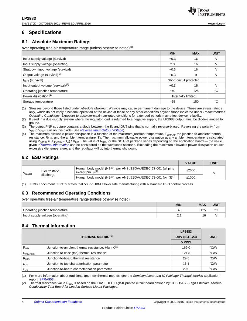
(1) Stresses beyond those listed under Absolute Maximum Ratings may cause permanent damage to the device. These are stress ratingsonly, which do not imply functional operation of the device at these or any other conditions beyond those indicated under RecommendedOperating Conditions. Exposure to absolute-maximum-rated conditions for extended periods may affect device reliability.
(2) If used in a dual-supply system where the regulator load is returned to a negative supply, the LP2983 output must be diode-clamped toground.
(3) The output PNP structure contains a diode between the IN and OUT pins that is normally reverse-biased. Reversing the polarity fromVIN to VOUT turn on this diode (See Reverse Input-Output Voltage).
(4) The maximum allowable power dissipation is a function of the maximum junction temperature, TJ(MAX), the junction-to-ambient thermalresistance, RθJA, and the ambient temperature, TA. The maximum allowable power dissipation at any ambient temperature is calculatedusing P(MAX) = (TJ(MAX) – TA) / RθJA. The value of RθJA for the SOT-23 package varies depending on the application board — the valuegiven inThermal Information can be considered as the worstcase scenario. Exceeding the maximum allowable power dissipation causesexcessive die temperature, and the regulator will go into thermal shutdown.
6 Specifications
6.1 Absolute Maximum Ratingsover operating free-air temperature range (unless otherwise noted) (1)
MIN MAX UNITInput supply voltage (survival) −0.3 16 VInput supply voltage (operating) 2.3 16 VShutdown input voltage (survival) −0.3 16 VOutput voltage (survival) (2) −0.3 9 VIOUT (survival) Short-circuit protectedInput-output voltage (survival) (3) −0.3 16 VOperating junction temperature −40 125 °CPower dissipation (4) Internally limitedStorage temperature –65 150 °C
(1) JEDEC document JEP155 states that 500-V HBM allows safe manufacturing with a standard ESD control process.
6.2 ESD RatingsVALUE UNIT
V(ESD)Electrostaticdischarge
Human body model (HBM), per ANSI/ESDA/JEDEC JS-001 (all pinsexcept pin 3) (1) ±2000
VHuman body model (HBM), per ANSI/ESDA/JEDEC JS-001 (pin 3) (1) ±1000
6.3 Recommended Operating Conditionsover operating free-air temperature range (unless otherwise noted)
MIN MAX UNITOperating junction temperature −40 125 °CInput supply voltage (operating) 2.2 16 V
(1) For more information about traditional and new thermal metrics, see the Semiconductor and IC Package Thermal Metrics applicationreport, SPRA953.
(2) Thermal resistance value RθJA is based on the EIA/JEDEC High-K printed circuit board defined by: JESD51-7 - High Effective ThermalConductivity Test Board for Leaded Surface Mount Packages.
6.4 Thermal Information
THERMAL METRIC (1)LP2983
UNITDBV (SOT-23)5 PINS
RθJA Junction-to-ambient thermal resistance, High-K (2) 169.0 °C/WRθJC(top) Junction-to-case (top) thermal resistance 121.8 °C/WRθJB Junction-to-board thermal resistance 29.5 °C/WψJT Junction-to-top characterization parameter 16.1 °C/WψJB Junction-to-board characterization parameter 29.0 °C/W
5
LP2983www.ti.com SNVS170D –OCTOBER 2001–REVISED APRIL 2016
Product Folder Links: LP2983
Submit Documentation FeedbackCopyright © 2001–2016, Texas Instruments Incorporated
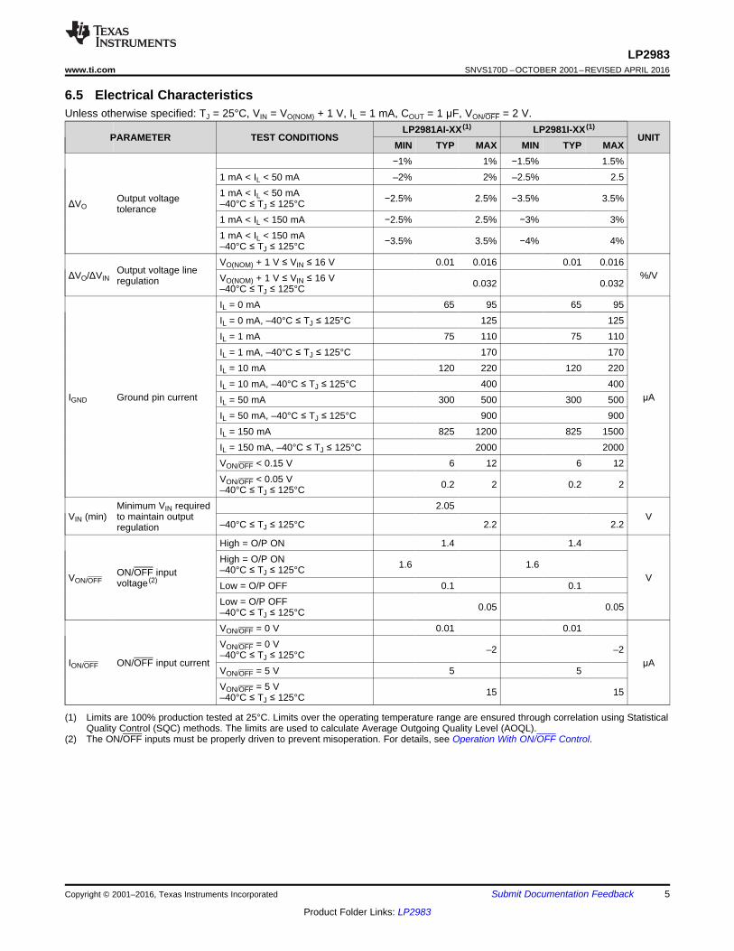
(1) Limits are 100% production tested at 25°C. Limits over the operating temperature range are ensured through correlation using StatisticalQuality Control (SQC) methods. The limits are used to calculate Average Outgoing Quality Level (AOQL).
(2) The ON/OFF inputs must be properly driven to prevent misoperation. For details, see Operation With ON/OFF Control.
6.5 Electrical CharacteristicsUnless otherwise specified: TJ = 25°C, VIN = VO(NOM) + 1 V, IL = 1 mA, COUT = 1 μF, VON/OFF = 2 V.
PARAMETER TEST CONDITIONSLP2981AI-XX (1) LP2981I-XX (1)
UNITMIN TYP MAX MIN TYP MAX
ΔVOOutput voltagetolerance
−1% 1% −1.5% 1.5%1 mA < IL < 50 mA –2% 2% –2.5% 2.51 mA < IL < 50 mA–40°C ≤ TJ ≤ 125°C −2.5% 2.5% −3.5% 3.5%
1 mA < IL < 150 mA −2.5% 2.5% −3% 3%1 mA < IL < 150 mA–40°C ≤ TJ ≤ 125°C −3.5% 3.5% −4% 4%
ΔVO/ΔVINOutput voltage lineregulation
VO(NOM) + 1 V ≤ VIN ≤ 16 V 0.01 0.016 0.01 0.016%/VVO(NOM) + 1 V ≤ VIN ≤ 16 V
–40°C ≤ TJ ≤ 125°C 0.032 0.032
IGND Ground pin current
IL = 0 mA 65 95 65 95
μA
IL = 0 mA, –40°C ≤ TJ ≤ 125°C 125 125IL = 1 mA 75 110 75 110IL = 1 mA, –40°C ≤ TJ ≤ 125°C 170 170IL = 10 mA 120 220 120 220IL = 10 mA, –40°C ≤ TJ ≤ 125°C 400 400IL = 50 mA 300 500 300 500IL = 50 mA, –40°C ≤ TJ ≤ 125°C 900 900IL = 150 mA 825 1200 825 1500IL = 150 mA, –40°C ≤ TJ ≤ 125°C 2000 2000VON/OFF < 0.15 V 6 12 6 12VON/OFF < 0.05 V–40°C ≤ TJ ≤ 125°C 0.2 2 0.2 2
VIN (min)Minimum VIN requiredto maintain outputregulation
2.05V
–40°C ≤ TJ ≤ 125°C 2.2 2.2
VON/OFFON/OFF inputvoltage (2)
High = O/P ON 1.4 1.4
V
High = O/P ON–40°C ≤ TJ ≤ 125°C 1.6 1.6
Low = O/P OFF 0.1 0.1Low = O/P OFF–40°C ≤ TJ ≤ 125°C 0.05 0.05
ION/OFF ON/OFF input current
VON/OFF = 0 V 0.01 0.01
μA
VON/OFF = 0 V–40°C ≤ TJ ≤ 125°C –2 –2
VON/OFF = 5 V 5 5VON/OFF = 5 V–40°C ≤ TJ ≤ 125°C 15 15
6
LP2983SNVS170D –OCTOBER 2001–REVISED APRIL 2016 www.ti.com
Product Folder Links: LP2983
Submit Documentation Feedback Copyright © 2001–2016, Texas Instruments Incorporated
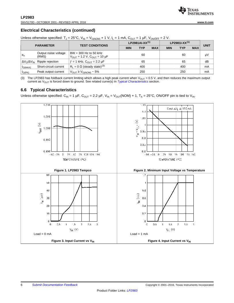
Electrical Characteristics (continued)Unless otherwise specified: TJ = 25°C, VIN = VO(NOM) + 1 V, IL = 1 mA, COUT = 1 μF, VON/OFF = 2 V.
PARAMETER TEST CONDITIONSLP2981AI-XX (1) LP2981I-XX (1)
UNITMIN TYP MAX MIN TYP MAX
(3) The LP2983 has foldback current limiting which allows a high peak current when VOUT > 0.5 V, and then reduces the maximum outputcurrent as VOUT is forced down to ground. See related curve(s) in Typical Characteristics section.
enOutput noise voltage(RMS)
BW = 300 Hz to 50 kHzVOUT = 1.2 V, COUT = 10 μF 60 60 μV
ΔVO/ΔVIN Ripple rejection ƒ = 1 kHz, COUT = 2.2 μF 65 65 dBIO(MAX) Short-circuit current RL = 0 Ω (steady state) (3) 400 400 mAIO(PK) Peak output current VOUT ≥ VO(NOM) − 5% 250 250 mA
6.6 Typical CharacteristicsUnless otherwise specified: CIN = 1 µF, COUT = 2.2 µF, VIN = VOUT(NOM) + 1, TA = 25°C, ON/OFF pin is tied to VIN.
Figure 1. LP2983 Tempco Figure 2. Minimum Input Voltage vs Temperature
Load = 0 mA
Figure 3. Input Current vs VIN
Load = 1 mA
Figure 4. Input Current vs VIN

7
LP2983www.ti.com SNVS170D –OCTOBER 2001–REVISED APRIL 2016
Product Folder Links: LP2983
Submit Documentation FeedbackCopyright © 2001–2016, Texas Instruments Incorporated
Typical Characteristics (continued)Unless otherwise specified: CIN = 1 µF, COUT = 2.2 µF, VIN = VOUT(NOM) + 1, TA = 25°C, ON/OFF pin is tied to VIN.
Load = 50 mA and 150 mA
Figure 5. Input Current vs VIN Figure 6. GND Pin vs Load Current
Figure 7. GND Pin vs Temperature and Load
Load = 1 mA ΔVIN = 1 V
Figure 8. Line Transient Response
Load = 150 mA ΔVIN = 1 V
Figure 9. Line Transient Response
Load = 1 mA ΔVIN = 13.8 V
Figure 10. Line Transient Response

8
LP2983SNVS170D –OCTOBER 2001–REVISED APRIL 2016 www.ti.com
Product Folder Links: LP2983
Submit Documentation Feedback Copyright © 2001–2016, Texas Instruments Incorporated
Typical Characteristics (continued)Unless otherwise specified: CIN = 1 µF, COUT = 2.2 µF, VIN = VOUT(NOM) + 1, TA = 25°C, ON/OFF pin is tied to VIN.
Load = 150 mA ΔVIN = 13.8 V
Figure 11. Line Transient Response Figure 12. Noise Density
COUT = 2.2 µF
Figure 13. Ripple Rejection Figure 14. Turnon Time
Figure 15. Short-Circuit Current vs Temperature
VIN = 16 V
Figure 16. Short-Circuit Current
9
LP2983www.ti.com SNVS170D –OCTOBER 2001–REVISED APRIL 2016
Product Folder Links: LP2983
Submit Documentation FeedbackCopyright © 2001–2016, Texas Instruments Incorporated
Typical Characteristics (continued)Unless otherwise specified: CIN = 1 µF, COUT = 2.2 µF, VIN = VOUT(NOM) + 1, TA = 25°C, ON/OFF pin is tied to VIN.
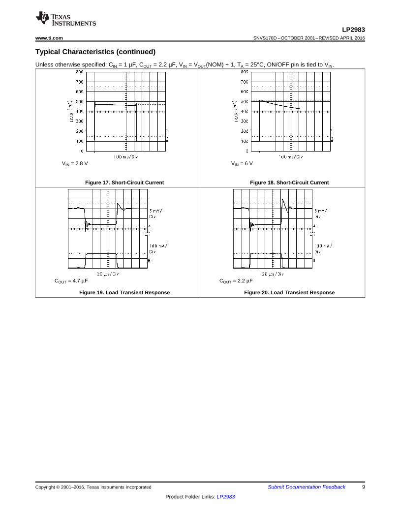
VIN = 2.8 V
Figure 17. Short-Circuit Current
VIN = 6 V
Figure 18. Short-Circuit Current
COUT = 4.7 µF
Figure 19. Load Transient Response
COUT = 2.2 µF
Figure 20. Load Transient Response

10
LP2983SNVS170D –OCTOBER 2001–REVISED APRIL 2016 www.ti.com
Product Folder Links: LP2983
Submit Documentation Feedback Copyright © 2001–2016, Texas Instruments Incorporated
7 Detailed Description
7.1 Overview
The LP2983 is a voltage regulator with optimized vertically integrated PNP designed for use with very low ESRoutput capacitors, excellent for low noise applications that require a clean voltage supply. The LP2983 has awide input voltage range (16 V maximum), high accuracy (A grade 1%), and a fixed output voltage supplycapable of delivering 150 mA. In addition the LP2983 device provides the following features:• High accuracy output voltage• Low ground current, typically 825 μA at 150-mA load and 75 μA at 1-mA load• A sleep mode feature is available, allowing the regulator to consume only 1 µA (typical) when the ON/OFF pin
is pulled low.• Overtemperature protection and overcurrent protection circuitry designed to safeguard the device during
unexpected conditions.• Thermal protection
7.2 Functional Block Diagram
7.3 Feature Description
7.3.1 High-Accuracy Output VoltageWith special careful design to minimize all contributions to the output voltage error, the LP2983 distinguishesitself as a very high-accuracy output voltage micropower LDO. This includes a tight initial tolerance (typically1.5% at 50 mA, 25°C junction temperature; also available in A grade with an accuracy of 1% under the sameconditions), extremely good line regulation (0.01%/V typical), and a very low output-voltage temperaturecoefficient, making the part an ideal low-power voltage reference.
7.3.2 Low Ground CurrentThe LP2983 device uses a vertical PNP process which allows for quiescent currents that are considerably lowerthan those associated with traditional lateral PNP regulators, typically 825 μA at 150-mA load and 75 μA at 1-mAload.
VIN VOUT
PNP
GND
SCHOTTKY DIODE
LP2983
Copyright © 2016, Texas Instruments Incorporated
VIN VOUT
PNP
GND
LP2983
Copyright © 2016, Texas Instruments Incorporated
11
LP2983www.ti.com SNVS170D –OCTOBER 2001–REVISED APRIL 2016
Product Folder Links: LP2983
Submit Documentation FeedbackCopyright © 2001–2016, Texas Instruments Incorporated
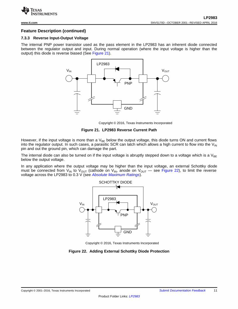
Feature Description (continued)7.3.3 Reverse Input-Output VoltageThe internal PNP power transistor used as the pass element in the LP2983 has an inherent diode connectedbetween the regulator output and input. During normal operation (where the input voltage is higher than theoutput) this diode is reverse biased (See Figure 21).
Figure 21. LP2983 Reverse Current Path
However, if the input voltage is more than a VBE below the output voltage, this diode turns ON and current flowsinto the regulator output. In such cases, a parasitic SCR can latch which allows a high current to flow into the VINpin and out the ground pin, which can damage the part.
The internal diode can also be turned on if the input voltage is abruptly stepped down to a voltage which is a VBEbelow the output voltage.
In any application where the output voltage may be higher than the input voltage, an external Schottky diodemust be connected from VIN to VOUT (cathode on VIN, anode on VOUT — see Figure 22), to limit the reversevoltage across the LP2983 to 0.3 V (see Absolute Maximum Ratings).
Figure 22. Adding External Schottky Diode Protection

12
LP2983SNVS170D –OCTOBER 2001–REVISED APRIL 2016 www.ti.com
Product Folder Links: LP2983
Submit Documentation Feedback Copyright © 2001–2016, Texas Instruments Incorporated
Feature Description (continued)7.3.4 ON/OFF Input OperationThe LP2983 is shut off by driving the ON/OFF input low, and turned on by pulling it high. If this feature is not tobe used, the ON/OFF input must be tied to VIN to keep the regulator output on at all times.
To assure proper operation, the signal source used to drive the ON/OFF input must be able to swing above andbelow the specified turnon or turnoff voltage thresholds listed in Typical Characteristics under VON/OFF. To preventmis-operation, the turnon (and turnoff) voltage signals applied to the ON/OFF input must have a slew rate whichis ≥ 40 mV/µs.
CAUTIONThe regulator output voltage can not be ensured if a slow-moving AC (or DC) signal isapplied that is in the range between the specified turn-on and turn-off voltages listedunder the electrical specification VON/OFF (see Electrical Characteristics).
7.3.5 Thermal ProtectionThe LP2983 contains a thermal shutdown protection circuit to turn off the output current when excessive heat isdissipated in the LDO. The thermal time-constant of the semiconductor die is fairly short, and thus the outputcycles on and off at a high rate when thermal shutdown is reached until the power dissipation is reduced. Theinternal protection circuitry of the LM2983 is designed to protect against thermal overload conditions. Thecircuitry is not intended to replace proper heat sinking. Continuously running the device into thermal shutdowndegrades its reliability.
7.4 Device Functional Modes
7.4.1 Operation With VO(NOM) + 1 V ≤ VIN < 16 VThe device operates if the input voltage is equal to, or exceeds, VOUT(TARGET) + 1 V. If the previous condition isnot met, the device will not operate correctly, and the output voltage may not reach target value.
7.4.2 Operation With ON/OFF ControlIf the voltage on the ON/OFF pin is less than 0.1 V at room temperature and less than 0.05 V over the fulloperating temperature range, the device output is disabled, and the shutdown current (IGND) will not exceed 12μA. Raising ON/OFF above 1.4 V at room temperature and above 1.6 V over the full operating temperaturerange initiates the start-up sequence of the device.
ON/OFFON/OFF*
GND
IN
ESR
OUT VOUTVIN
2.2 µF
1 µF
Copyright © 2016, Texas Instruments Incorporated
13
LP2983www.ti.com SNVS170D –OCTOBER 2001–REVISED APRIL 2016
Product Folder Links: LP2983
Submit Documentation FeedbackCopyright © 2001–2016, Texas Instruments Incorporated
8 Application and Implementation
NOTEInformation in the following applications sections is not part of the TI componentspecification, and TI does not warrant its accuracy or completeness. TI’s customers areresponsible for determining suitability of components for their purposes. Customers shouldvalidate and test their design implementation to confirm system functionality.
8.1 Application InformationThe LP2983 is a linear voltage regulator operating from 2.2 V to 16 V on the input and regulates voltagesbetween ≤ 1.2 V with high accuracy and a 150-mA maximum output current. To achieve high efficiency, thedropout voltage (VIN – VOUT) must be as small as possible. Successfully implementing an LDO in an applicationdepends on the application requirements. If the requirements are simply input voltage and output voltage,compliance specifications (such as internal power dissipation or stability) must be verified to ensure performance.
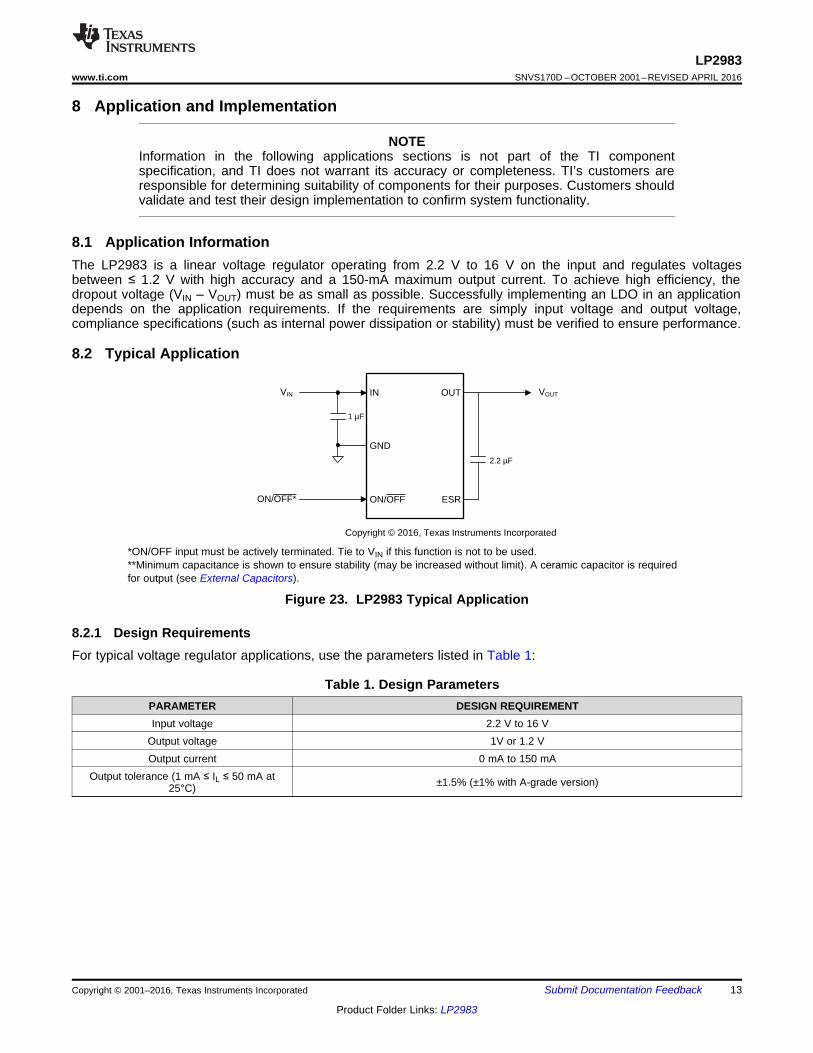
8.2 Typical Application
*ON/OFF input must be actively terminated. Tie to VIN if this function is not to be used.**Minimum capacitance is shown to ensure stability (may be increased without limit). A ceramic capacitor is requiredfor output (see External Capacitors).
Figure 23. LP2983 Typical Application
8.2.1 Design RequirementsFor typical voltage regulator applications, use the parameters listed in Table 1:
Table 1. Design ParametersPARAMETER DESIGN REQUIREMENTInput voltage 2.2 V to 16 V
Output voltage 1V or 1.2 VOutput current 0 mA to 150 mA
Output tolerance (1 mA ≤ IL ≤ 50 mA at25°C) ±1.5% (±1% with A-grade version)
14
LP2983SNVS170D –OCTOBER 2001–REVISED APRIL 2016 www.ti.com
Product Folder Links: LP2983
Submit Documentation Feedback Copyright © 2001–2016, Texas Instruments Incorporated
8.2.2 Detailed Design Procedure
8.2.2.1 External CapacitorsLike any low-dropout regulator, the LP2983 requires external capacitors for regulator stability. These capacitorsmust be correctly selected for good performance.
8.2.2.1.1 Input Capacitor
An input capacitor whose capacitance is ≥ 1 µF is required between the LP2983 input and ground (the amount ofcapacitance may be increased without limit).
This capacitor must be located a distance of not more than 1 cm from the input pin and returned to a cleananalog ground. Any good-quality ceramic, tantalum, or film capacitor may be used at the input.
NOTETantalum capacitors can suffer catastrophic failure due to surge current when connectedto a low-impedance source of power (like a battery or very large capacitor). If a tantalumcapacitor is used at the input, it must be ensured by the manufacturer to have a surgecurrent rating sufficient for the application.
There are no requirements for ESR on the input capacitor, but tolerance and temperature coefficient must beconsidered when selecting the capacitor to ensure the capacitance is ≥ 1 µF over the entire operatingtemperature range.
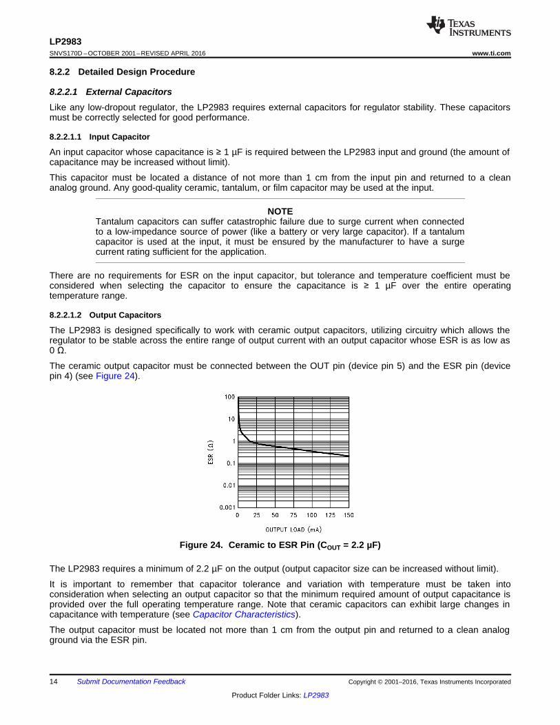
8.2.2.1.2 Output Capacitors
The LP2983 is designed specifically to work with ceramic output capacitors, utilizing circuitry which allows theregulator to be stable across the entire range of output current with an output capacitor whose ESR is as low as0 Ω.
The ceramic output capacitor must be connected between the OUT pin (device pin 5) and the ESR pin (devicepin 4) (see Figure 24).
Figure 24. Ceramic to ESR Pin (COUT = 2.2 µF)
The LP2983 requires a minimum of 2.2 µF on the output (output capacitor size can be increased without limit).
It is important to remember that capacitor tolerance and variation with temperature must be taken intoconsideration when selecting an output capacitor so that the minimum required amount of output capacitance isprovided over the full operating temperature range. Note that ceramic capacitors can exhibit large changes incapacitance with temperature (see Capacitor Characteristics).
The output capacitor must be located not more than 1 cm from the output pin and returned to a clean analogground via the ESR pin.
15
LP2983www.ti.com SNVS170D –OCTOBER 2001–REVISED APRIL 2016
Product Folder Links: LP2983
Submit Documentation FeedbackCopyright © 2001–2016, Texas Instruments Incorporated
8.2.2.2 Capacitor Characteristics
The LP2983 was designed to work with ceramic capacitors on the output to take advantage of the benefits theyoffer: for capacitance values in the 2.2-µF to 4.7-µF range, ceramics are the least expensive and also have thelowest ESR values (which makes them best for eliminating high-frequency noise).
One disadvantage of ceramic capacitors is that their capacitance can vary with temperature. Most large valueceramic capacitors (≥ 2.2 µF) are manufactured with the Z5U or Y5V temperature characteristic, which results inthe capacitance dropping by more than 50% as the temperature goes from 25°C to 85°C.
This could cause problems if a 2.2-µF capacitor were used on the output since it will drop down to approximately1 µF at high ambient temperatures (which could cause the LP2983 to oscillate). If Z5U or Y5V capacitors areused on the output, a minimum capacitance value of 4.7 µF must be observed.
A better choice for temperature coefficient in ceramic capacitors is X7R, which holds the capacitance within±15%. Unfortunately, the larger values of capacitance are not offered by all manufacturers in the X7R dielectric.
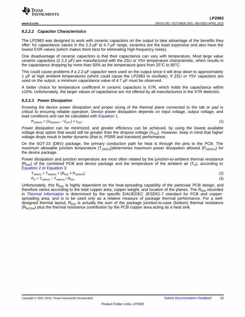
8.2.2.3 Power DissipationKnowing the device power dissipation and proper sizing of the thermal plane connected to the tab or pad iscritical to ensuring reliable operation. Device power dissipation depends on input voltage, output voltage, andload conditions and can be calculated with Equation 1.
PD(MAX) = (VIN(MAX) – VOUT) × IOUT (1)
Power dissipation can be minimized, and greater efficiency can be achieved, by using the lowest availablevoltage drop option that would still be greater than the dropout voltage (VDO). However, keep in mind that highervoltage drops result in better dynamic (that is, PSRR and transient) performance.
On the SOT-23 (DBV) package, the primary conduction path for heat is through the pins to the PCB. Themaximum allowable junction temperature (TJ(MAX))determines maximum power dissipation allowed (PD(MAX)) forthe device package.
Power dissipation and junction temperature are most often related by the junction-to-ambient thermal resistance(RθJA) of the combined PCB and device package and the temperature of the ambient air (TA), according toEquation 2 or Equation 3:
TJ(MAX) = TA(MAX) + (RθJA × PD(MAX)) (2)PD = TJ(MAX) – TA(MAX) / RθJA (3)
Unfortunately, this RθJA is highly dependent on the heat-spreading capability of the particular PCB design, andtherefore varies according to the total copper area, copper weight, and location of the planes. The RθJA recordedin Thermal Information is determined by the specific EIA/JEDEC JESD51-7 standard for PCB and copper-spreading area, and is to be used only as a relative measure of package thermal performance. For a well-designed thermal layout, RθJA is actually the sum of the package junction-to-case (bottom) thermal resistance(RθJCbot) plus the thermal resistance contribution by the PCB copper area acting as a heat sink.

16
LP2983SNVS170D –OCTOBER 2001–REVISED APRIL 2016 www.ti.com
Product Folder Links: LP2983
Submit Documentation Feedback Copyright © 2001–2016, Texas Instruments Incorporated
8.2.2.4 Estimating Junction TemperatureThe EIA/JEDEC standard recommends the use of psi (Ψ) thermal characteristics to estimate the junctiontemperatures of surface mount devices on a typical PCB board application. These characteristics are not truethermal resistance values, but rather package specific thermal characteristics that offer practical and relativemeans of estimating junction temperatures. These psi metrics are determined to be significantly independent ofcopper-spreading area. The key thermal characteristics (ΨJT and ΨJB) are given in Thermal Information and areused in accordance with Equation 4 or Equation 5.
TJ(MAX) = TTOP + (ΨJT × PD(MAX))
where• PD(MAX) is explained in Equation 3• TTOP is the temperature measured at the center-top of the device package. (4)
TJ(MAX) = TBOARD + (ΨJB × PD(MAX))
where• PD(MAX) is explained in Equation 3.• TBOARD is the PCB surface temperature measured 1-mm from the device package and centered on the
package edge. (5)
For more information about the thermal characteristics ΨJT and ΨJB, see Semiconductor and IC PackageThermal Metrics (SPRA953); for more information about measuring TTOP and TBOARD, see Using New ThermalMetrics (SBVA025); and for more information about the EIA/JEDEC JESD51 PCB used for validating RθJA, seeThermal Characteristics of Linear and Logic Packages Using JEDEC PCB Designs (SZZA017). Theseapplication notes are available at www.ti.com.
8.2.3 Application CurvesUnless otherwise specified, CIN = 1 μF, COUT = 2.2 μF, VIN = VOUT(NOM) + 1, TA = 25°C, ON/OFF pin is tied to VIN..
Figure 25. Line Transient Response Figure 26. Load Transient Response
9 Power Supply RecommendationsThe LP2983 is designed to operate from an input voltage supply range between 2.2 V and 16 V. The inputvoltage range provides adequate headroom for the device to have a regulated output. This input supply must bewell regulated. If the input supply is noisy, additional input capacitors with low ESR can help improve the outputnoise and transient performance.

IN
GND
ON/OFF
OUT
ESR
Ground
VOUTVIN
Input Capacitor
Output Capacitor
ON/OFF
17
LP2983www.ti.com SNVS170D –OCTOBER 2001–REVISED APRIL 2016
Product Folder Links: LP2983
Submit Documentation FeedbackCopyright © 2001–2016, Texas Instruments Incorporated
10 Layout
10.1 Layout GuidelinesFor best overall performance, place all circuit components on the same side of the circuit board and as near aspractical to the respective LDO pin connections. Place ground return connections to the input and outputcapacitors, and to the LDO ground pin as close to each other as possible, connected by a wide, component-side,copper surface. The use of vias and long traces to create LDO circuit connections is strongly discouraged andnegatively affects system performance. This grounding and layout scheme minimizes inductive parasitics, andthereby reduces load-current transients, minimizes noise, and increases circuit stability. TI also recommends aground reference plane, either embedded in the PCB itself or located on the bottom side of the PCB opposite thecomponents. This reference plane serves to assure accuracy of the output voltage, shield noise, and behavessimilar to a thermal plane to spread (or sink) heat from the LDO device. In most applications, this ground plane isnecessary to meet thermal requirements.
10.2 Layout Example
Figure 27. LP2983 Layout Example

18
LP2983SNVS170D –OCTOBER 2001–REVISED APRIL 2016 www.ti.com
Product Folder Links: LP2983
Submit Documentation Feedback Copyright © 2001–2016, Texas Instruments Incorporated
11 Device and Documentation Support
11.1 Documentation Support
11.1.1 Related DocumentationFor additional information, see the following:• Semiconductor and IC Package Thermal Metrics (SPRA953)• Using New Thermal Metrics (SBVA025)• Thermal Characteristics of Linear and Logic Packages Using JEDEC PCB Designs (SZZA017)
11.2 Community ResourcesThe following links connect to TI community resources. Linked contents are provided "AS IS" by the respectivecontributors. They do not constitute TI specifications and do not necessarily reflect TI's views; see TI's Terms ofUse.
TI E2E™ Online Community TI's Engineer-to-Engineer (E2E) Community. Created to foster collaborationamong engineers. At e2e.ti.com, you can ask questions, share knowledge, explore ideas and helpsolve problems with fellow engineers.
Design Support TI's Design Support Quickly find helpful E2E forums along with design support tools andcontact information for technical support.
11.3 TrademarksE2E is a trademark of Texas Instruments.All other trademarks are the property of their respective owners.
11.4 Electrostatic Discharge CautionThese devices have limited built-in ESD protection. The leads should be shorted together or the device placed in conductive foamduring storage or handling to prevent electrostatic damage to the MOS gates.
11.5 GlossarySLYZ022 — TI Glossary.
This glossary lists and explains terms, acronyms, and definitions.
12 Mechanical, Packaging, and Orderable InformationThe following pages include mechanical, packaging, and orderable information. This information is the mostcurrent data available for the designated devices. This data is subject to change without notice and revision ofthis document. For browser-based versions of this data sheet, refer to the left-hand navigation.
PACKAGE OPTION ADDENDUM
www.ti.com 17-Mar-2017
Addendum-Page 1
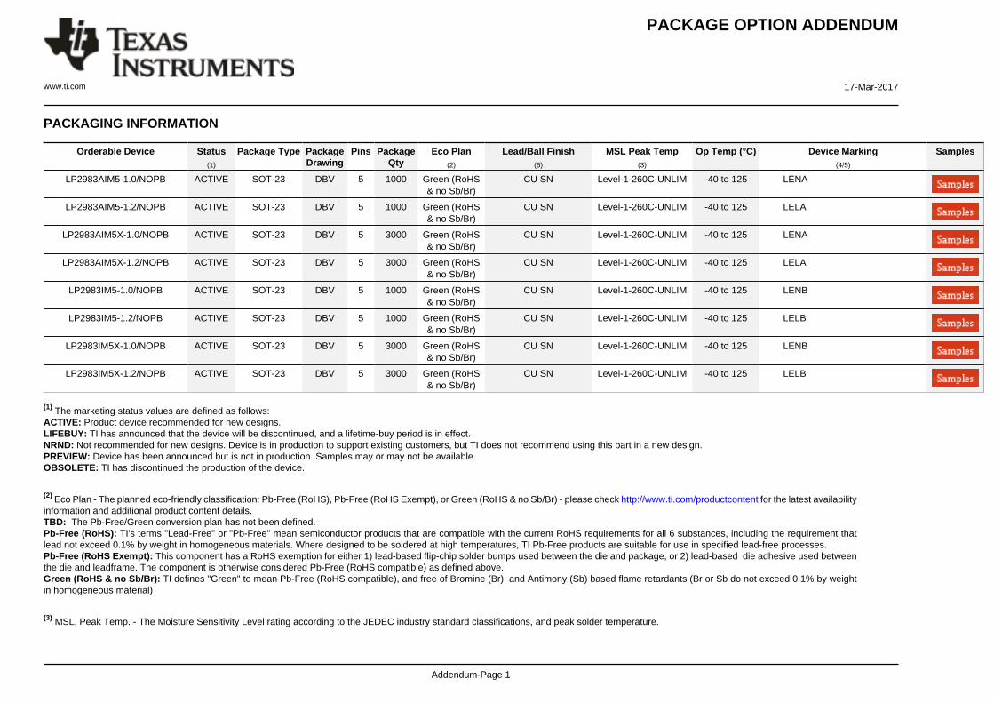
PACKAGING INFORMATION
Orderable Device Status(1)
Package Type PackageDrawing
Pins PackageQty
Eco Plan(2)
Lead/Ball Finish(6)
MSL Peak Temp(3)
Op Temp (°C) Device Marking(4/5)
Samples
LP2983AIM5-1.0/NOPB ACTIVE SOT-23 DBV 5 1000 Green (RoHS& no Sb/Br)
CU SN Level-1-260C-UNLIM -40 to 125 LENA
LP2983AIM5-1.2/NOPB ACTIVE SOT-23 DBV 5 1000 Green (RoHS& no Sb/Br)
CU SN Level-1-260C-UNLIM -40 to 125 LELA
LP2983AIM5X-1.0/NOPB ACTIVE SOT-23 DBV 5 3000 Green (RoHS& no Sb/Br)
CU SN Level-1-260C-UNLIM -40 to 125 LENA
LP2983AIM5X-1.2/NOPB ACTIVE SOT-23 DBV 5 3000 Green (RoHS& no Sb/Br)
CU SN Level-1-260C-UNLIM -40 to 125 LELA
LP2983IM5-1.0/NOPB ACTIVE SOT-23 DBV 5 1000 Green (RoHS& no Sb/Br)
CU SN Level-1-260C-UNLIM -40 to 125 LENB
LP2983IM5-1.2/NOPB ACTIVE SOT-23 DBV 5 1000 Green (RoHS& no Sb/Br)
CU SN Level-1-260C-UNLIM -40 to 125 LELB
LP2983IM5X-1.0/NOPB ACTIVE SOT-23 DBV 5 3000 Green (RoHS& no Sb/Br)
CU SN Level-1-260C-UNLIM -40 to 125 LENB
LP2983IM5X-1.2/NOPB ACTIVE SOT-23 DBV 5 3000 Green (RoHS& no Sb/Br)
CU SN Level-1-260C-UNLIM -40 to 125 LELB
(1) The marketing status values are defined as follows:ACTIVE: Product device recommended for new designs.LIFEBUY: TI has announced that the device will be discontinued, and a lifetime-buy period is in effect.NRND: Not recommended for new designs. Device is in production to support existing customers, but TI does not recommend using this part in a new design.PREVIEW: Device has been announced but is not in production. Samples may or may not be available.OBSOLETE: TI has discontinued the production of the device.
(2) Eco Plan - The planned eco-friendly classification: Pb-Free (RoHS), Pb-Free (RoHS Exempt), or Green (RoHS & no Sb/Br) - please check http://www.ti.com/productcontent for the latest availabilityinformation and additional product content details.TBD: The Pb-Free/Green conversion plan has not been defined.Pb-Free (RoHS): TI's terms "Lead-Free" or "Pb-Free" mean semiconductor products that are compatible with the current RoHS requirements for all 6 substances, including the requirement thatlead not exceed 0.1% by weight in homogeneous materials. Where designed to be soldered at high temperatures, TI Pb-Free products are suitable for use in specified lead-free processes.Pb-Free (RoHS Exempt): This component has a RoHS exemption for either 1) lead-based flip-chip solder bumps used between the die and package, or 2) lead-based die adhesive used betweenthe die and leadframe. The component is otherwise considered Pb-Free (RoHS compatible) as defined above.Green (RoHS & no Sb/Br): TI defines "Green" to mean Pb-Free (RoHS compatible), and free of Bromine (Br) and Antimony (Sb) based flame retardants (Br or Sb do not exceed 0.1% by weightin homogeneous material)
(3) MSL, Peak Temp. - The Moisture Sensitivity Level rating according to the JEDEC industry standard classifications, and peak solder temperature.

PACKAGE OPTION ADDENDUM
www.ti.com 17-Mar-2017
Addendum-Page 2
(4) There may be additional marking, which relates to the logo, the lot trace code information, or the environmental category on the device.
(5) Multiple Device Markings will be inside parentheses. Only one Device Marking contained in parentheses and separated by a "~" will appear on a device. If a line is indented then it is a continuationof the previous line and the two combined represent the entire Device Marking for that device.
(6) Lead/Ball Finish - Orderable Devices may have multiple material finish options. Finish options are separated by a vertical ruled line. Lead/Ball Finish values may wrap to two lines if the finishvalue exceeds the maximum column width.
Important Information and Disclaimer:The information provided on this page represents TI's knowledge and belief as of the date that it is provided. TI bases its knowledge and belief on informationprovided by third parties, and makes no representation or warranty as to the accuracy of such information. Efforts are underway to better integrate information from third parties. TI has taken andcontinues to take reasonable steps to provide representative and accurate information but may not have conducted destructive testing or chemical analysis on incoming materials and chemicals.TI and TI suppliers consider certain information to be proprietary, and thus CAS numbers and other limited information may not be available for release.
In no event shall TI's liability arising out of such information exceed the total purchase price of the TI part(s) at issue in this document sold by TI to Customer on an annual basis.
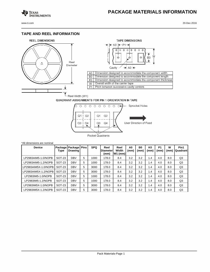
TAPE AND REEL INFORMATION
*All dimensions are nominal
Device PackageType
PackageDrawing
Pins SPQ ReelDiameter
(mm)
ReelWidth
W1 (mm)
A0(mm)
B0(mm)
K0(mm)
P1(mm)
W(mm)
Pin1Quadrant
LP2983AIM5-1.0/NOPB SOT-23 DBV 5 1000 178.0 8.4 3.2 3.2 1.4 4.0 8.0 Q3
LP2983AIM5-1.2/NOPB SOT-23 DBV 5 1000 178.0 8.4 3.2 3.2 1.4 4.0 8.0 Q3
LP2983AIM5X-1.0/NOPB SOT-23 DBV 5 3000 178.0 8.4 3.2 3.2 1.4 4.0 8.0 Q3
LP2983AIM5X-1.2/NOPB SOT-23 DBV 5 3000 178.0 8.4 3.2 3.2 1.4 4.0 8.0 Q3
LP2983IM5-1.0/NOPB SOT-23 DBV 5 1000 178.0 8.4 3.2 3.2 1.4 4.0 8.0 Q3
LP2983IM5-1.2/NOPB SOT-23 DBV 5 1000 178.0 8.4 3.2 3.2 1.4 4.0 8.0 Q3
LP2983IM5X-1.0/NOPB SOT-23 DBV 5 3000 178.0 8.4 3.2 3.2 1.4 4.0 8.0 Q3
LP2983IM5X-1.2/NOPB SOT-23 DBV 5 3000 178.0 8.4 3.2 3.2 1.4 4.0 8.0 Q3
PACKAGE MATERIALS INFORMATION
www.ti.com 20-Dec-2016
Pack Materials-Page 1
*All dimensions are nominal
Device Package Type Package Drawing Pins SPQ Length (mm) Width (mm) Height (mm)
LP2983AIM5-1.0/NOPB SOT-23 DBV 5 1000 210.0 185.0 35.0
LP2983AIM5-1.2/NOPB SOT-23 DBV 5 1000 210.0 185.0 35.0
LP2983AIM5X-1.0/NOPB SOT-23 DBV 5 3000 210.0 185.0 35.0
LP2983AIM5X-1.2/NOPB SOT-23 DBV 5 3000 210.0 185.0 35.0
LP2983IM5-1.0/NOPB SOT-23 DBV 5 1000 210.0 185.0 35.0
LP2983IM5-1.2/NOPB SOT-23 DBV 5 1000 210.0 185.0 35.0
LP2983IM5X-1.0/NOPB SOT-23 DBV 5 3000 210.0 185.0 35.0
LP2983IM5X-1.2/NOPB SOT-23 DBV 5 3000 210.0 185.0 35.0
PACKAGE MATERIALS INFORMATION
www.ti.com 20-Dec-2016
Pack Materials-Page 2

www.ti.com
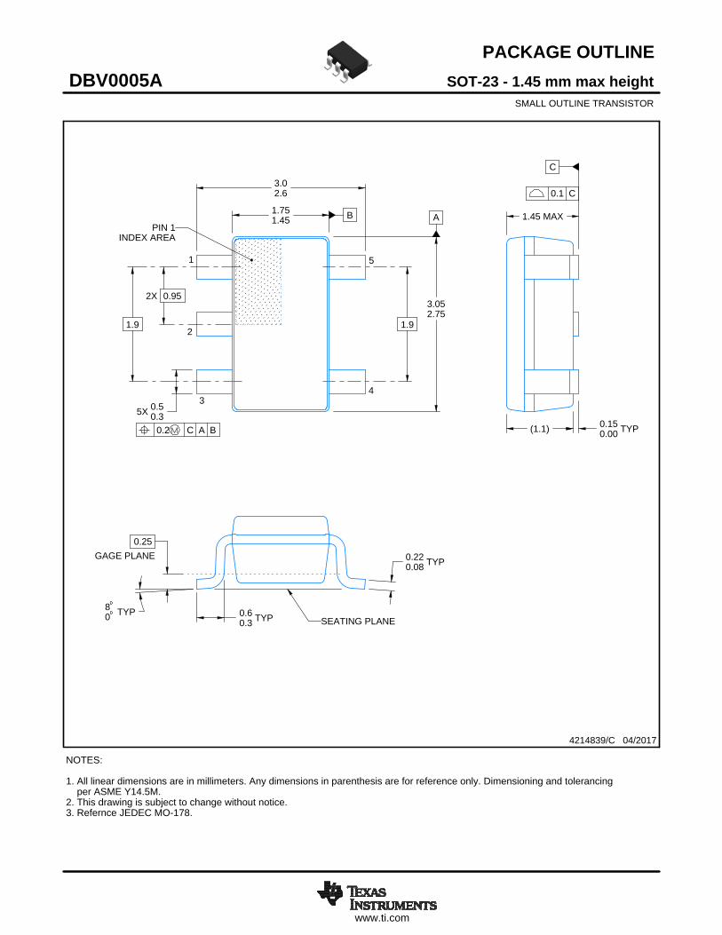
PACKAGE OUTLINE
C
TYP0.220.08
0.25
3.02.6
2X 0.95
1.9
1.45 MAX
TYP0.150.00
5X 0.50.3
TYP0.60.3
TYP80
1.9
A
3.052.75
B1.751.45
(1.1)
SOT-23 - 1.45 mm max heightDBV0005ASMALL OUTLINE TRANSISTOR
4214839/C 04/2017
NOTES: 1. All linear dimensions are in millimeters. Any dimensions in parenthesis are for reference only. Dimensioning and tolerancing per ASME Y14.5M.2. This drawing is subject to change without notice.3. Refernce JEDEC MO-178.
0.2 C A B
1
34
5
2
INDEX AREAPIN 1
GAGE PLANE
SEATING PLANE
0.1 C
SCALE 4.000
www.ti.com
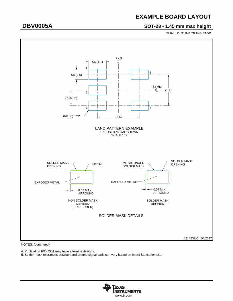
EXAMPLE BOARD LAYOUT
0.07 MAXARROUND
0.07 MINARROUND
5X (1.1)
5X (0.6)
(2.6)
(1.9)
2X (0.95)
(R0.05) TYP
4214839/C 04/2017
SOT-23 - 1.45 mm max heightDBV0005ASMALL OUTLINE TRANSISTOR
NOTES: (continued) 4. Publication IPC-7351 may have alternate designs. 5. Solder mask tolerances between and around signal pads can vary based on board fabrication site.
SYMM
LAND PATTERN EXAMPLEEXPOSED METAL SHOWN
SCALE:15X
PKG
1
3 4
5
2
SOLDER MASKOPENINGMETAL UNDER
SOLDER MASK
SOLDER MASKDEFINED
EXPOSED METAL
METALSOLDER MASKOPENING
NON SOLDER MASKDEFINED
(PREFERRED)
SOLDER MASK DETAILS
EXPOSED METAL

www.ti.com
EXAMPLE STENCIL DESIGN
(2.6)
(1.9)
2X(0.95)
5X (1.1)
5X (0.6)
(R0.05) TYP
SOT-23 - 1.45 mm max heightDBV0005ASMALL OUTLINE TRANSISTOR
4214839/C 04/2017
NOTES: (continued) 6. Laser cutting apertures with trapezoidal walls and rounded corners may offer better paste release. IPC-7525 may have alternate design recommendations. 7. Board assembly site may have different recommendations for stencil design.
SOLDER PASTE EXAMPLEBASED ON 0.125 mm THICK STENCIL
SCALE:15X
SYMM
PKG
1
3 4
5
2

IMPORTANT NOTICE
Texas Instruments Incorporated (TI) reserves the right to make corrections, enhancements, improvements and other changes to itssemiconductor products and services per JESD46, latest issue, and to discontinue any product or service per JESD48, latest issue. Buyersshould obtain the latest relevant information before placing orders and should verify that such information is current and complete.TI’s published terms of sale for semiconductor products (http://www.ti.com/sc/docs/stdterms.htm) apply to the sale of packaged integratedcircuit products that TI has qualified and released to market. Additional terms may apply to the use or sale of other types of TI products andservices.Reproduction of significant portions of TI information in TI data sheets is permissible only if reproduction is without alteration and isaccompanied by all associated warranties, conditions, limitations, and notices. TI is not responsible or liable for such reproduceddocumentation. Information of third parties may be subject to additional restrictions. Resale of TI products or services with statementsdifferent from or beyond the parameters stated by TI for that product or service voids all express and any implied warranties for theassociated TI product or service and is an unfair and deceptive business practice. TI is not responsible or liable for any such statements.Buyers and others who are developing systems that incorporate TI products (collectively, “Designers”) understand and agree that Designersremain responsible for using their independent analysis, evaluation and judgment in designing their applications and that Designers havefull and exclusive responsibility to assure the safety of Designers' applications and compliance of their applications (and of all TI productsused in or for Designers’ applications) with all applicable regulations, laws and other applicable requirements. Designer represents that, withrespect to their applications, Designer has all the necessary expertise to create and implement safeguards that (1) anticipate dangerousconsequences of failures, (2) monitor failures and their consequences, and (3) lessen the likelihood of failures that might cause harm andtake appropriate actions. Designer agrees that prior to using or distributing any applications that include TI products, Designer willthoroughly test such applications and the functionality of such TI products as used in such applications.TI’s provision of technical, application or other design advice, quality characterization, reliability data or other services or information,including, but not limited to, reference designs and materials relating to evaluation modules, (collectively, “TI Resources”) are intended toassist designers who are developing applications that incorporate TI products; by downloading, accessing or using TI Resources in anyway, Designer (individually or, if Designer is acting on behalf of a company, Designer’s company) agrees to use any particular TI Resourcesolely for this purpose and subject to the terms of this Notice.TI’s provision of TI Resources does not expand or otherwise alter TI’s applicable published warranties or warranty disclaimers for TIproducts, and no additional obligations or liabilities arise from TI providing such TI Resources. TI reserves the right to make corrections,enhancements, improvements and other changes to its TI Resources. TI has not conducted any testing other than that specificallydescribed in the published documentation for a particular TI Resource.Designer is authorized to use, copy and modify any individual TI Resource only in connection with the development of applications thatinclude the TI product(s) identified in such TI Resource. NO OTHER LICENSE, EXPRESS OR IMPLIED, BY ESTOPPEL OR OTHERWISETO ANY OTHER TI INTELLECTUAL PROPERTY RIGHT, AND NO LICENSE TO ANY TECHNOLOGY OR INTELLECTUAL PROPERTYRIGHT OF TI OR ANY THIRD PARTY IS GRANTED HEREIN, including but not limited to any patent right, copyright, mask work right, orother intellectual property right relating to any combination, machine, or process in which TI products or services are used. Informationregarding or referencing third-party products or services does not constitute a license to use such products or services, or a warranty orendorsement thereof. Use of TI Resources may require a license from a third party under the patents or other intellectual property of thethird party, or a license from TI under the patents or other intellectual property of TI.TI RESOURCES ARE PROVIDED “AS IS” AND WITH ALL FAULTS. TI DISCLAIMS ALL OTHER WARRANTIES ORREPRESENTATIONS, EXPRESS OR IMPLIED, REGARDING RESOURCES OR USE THEREOF, INCLUDING BUT NOT LIMITED TOACCURACY OR COMPLETENESS, TITLE, ANY EPIDEMIC FAILURE WARRANTY AND ANY IMPLIED WARRANTIES OFMERCHANTABILITY, FITNESS FOR A PARTICULAR PURPOSE, AND NON-INFRINGEMENT OF ANY THIRD PARTY INTELLECTUALPROPERTY RIGHTS. TI SHALL NOT BE LIABLE FOR AND SHALL NOT DEFEND OR INDEMNIFY DESIGNER AGAINST ANY CLAIM,INCLUDING BUT NOT LIMITED TO ANY INFRINGEMENT CLAIM THAT RELATES TO OR IS BASED ON ANY COMBINATION OFPRODUCTS EVEN IF DESCRIBED IN TI RESOURCES OR OTHERWISE. IN NO EVENT SHALL TI BE LIABLE FOR ANY ACTUAL,DIRECT, SPECIAL, COLLATERAL, INDIRECT, PUNITIVE, INCIDENTAL, CONSEQUENTIAL OR EXEMPLARY DAMAGES INCONNECTION WITH OR ARISING OUT OF TI RESOURCES OR USE THEREOF, AND REGARDLESS OF WHETHER TI HAS BEENADVISED OF THE POSSIBILITY OF SUCH DAMAGES.Unless TI has explicitly designated an individual product as meeting the requirements of a particular industry standard (e.g., ISO/TS 16949and ISO 26262), TI is not responsible for any failure to meet such industry standard requirements.Where TI specifically promotes products as facilitating functional safety or as compliant with industry functional safety standards, suchproducts are intended to help enable customers to design and create their own applications that meet applicable functional safety standardsand requirements. Using products in an application does not by itself establish any safety features in the application. Designers mustensure compliance with safety-related requirements and standards applicable to their applications. Designer may not use any TI products inlife-critical medical equipment unless authorized officers of the parties have executed a special contract specifically governing such use.Life-critical medical equipment is medical equipment where failure of such equipment would cause serious bodily injury or death (e.g., lifesupport, pacemakers, defibrillators, heart pumps, neurostimulators, and implantables). Such equipment includes, without limitation, allmedical devices identified by the U.S. Food and Drug Administration as Class III devices and equivalent classifications outside the U.S.TI may expressly designate certain products as completing a particular qualification (e.g., Q100, Military Grade, or Enhanced Product).Designers agree that it has the necessary expertise to select the product with the appropriate qualification designation for their applicationsand that proper product selection is at Designers’ own risk. Designers are solely responsible for compliance with all legal and regulatoryrequirements in connection with such selection.Designer will fully indemnify TI and its representatives against any damages, costs, losses, and/or liabilities arising out of Designer’s non-compliance with the terms and provisions of this Notice.
Mailing Address: Texas Instruments, Post Office Box 655303, Dallas, Texas 75265Copyright © 2018, Texas Instruments Incorporated