lpc4088 developer’s kit user’s guide - farnell … interface & connector (provision for...
TRANSCRIPT
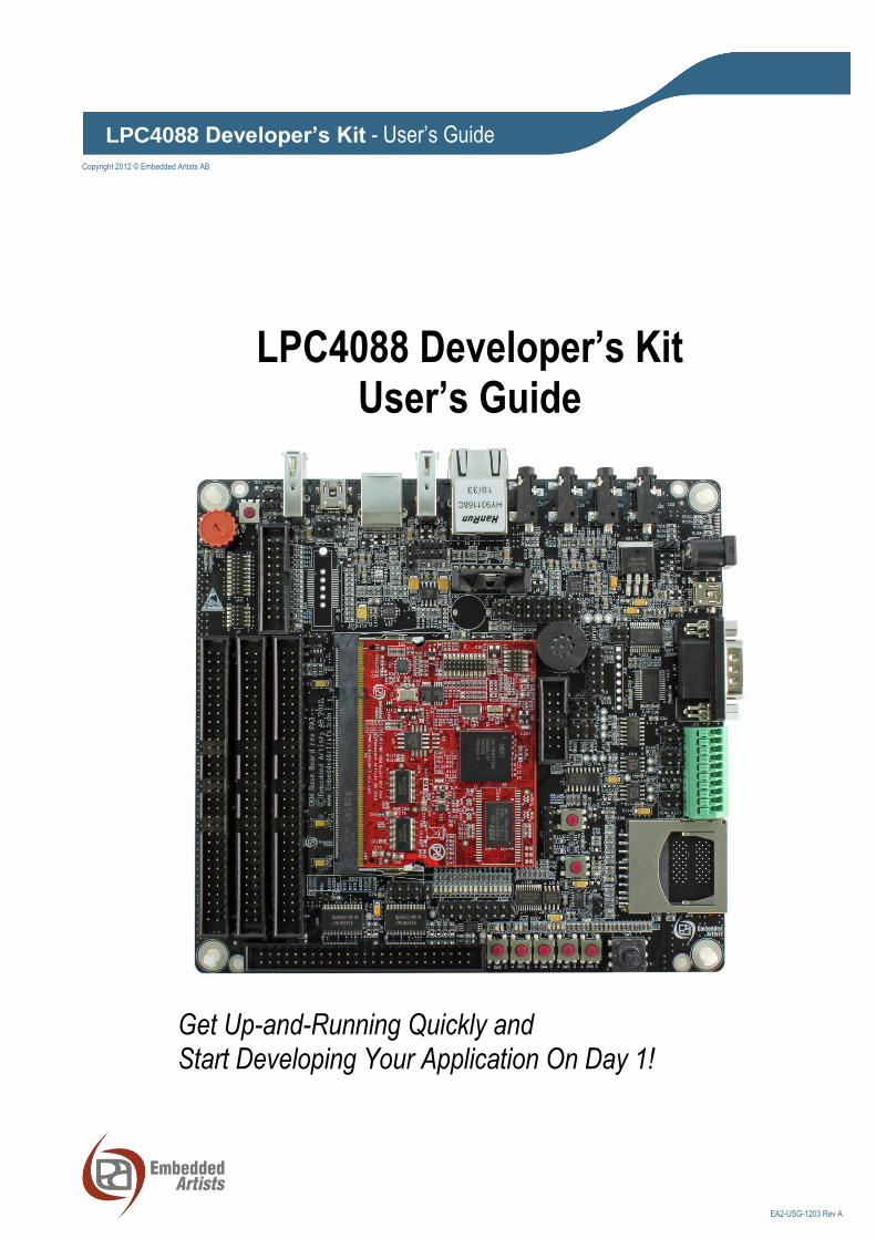
LPC4088 Developer’s Kit - User’s Guide
Copyright 2012 © Embedded Artists AB
EA2-USG-1203 Rev A
LPC4088 Developer’s Kit User’s Guide
Get Up-and-Running Quickly and Start Developing Your Application On Day 1!
LPC4088 Developer’s Kit - User’s Guide Page 2
Copyright 2012 © Embedded Artists AB
Embedded Artists AB Davidshallsgatan 16 211 45 Malmö Sweden
[email protected] http://www.EmbeddedArtists.com
Copyright 2012 © Embedded Artists AB. All rights reserved.
No part of this publication may be reproduced, transmitted, transcribed, stored in a retrieval system, or translated into any language or computer language, in any form or by any means, electronic, mechanical, magnetic, optical, chemical, manual or otherwise, without the prior written permission of Embedded Artists AB.
Disclaimer
Embedded Artists AB makes no representation or warranties with respect to the contents hereof and specifically disclaim any implied warranties or merchantability or fitness for any particular purpose. Information in this publication is subject to change without notice and does not represent a commitment on the part of Embedded Artists AB.
Feedback
We appreciate any feedback you may have for improvements on this document. Please send your comments to [email protected].
Trademarks
All brand and product names mentioned herein are trademarks, services marks, registered trademarks, or registered service marks of their respective owners and should be treated as such.
LPC4088 Developer’s Kit - User’s Guide Page 3
Copyright 2012 © Embedded Artists AB
Table of Contents 1 Document Revision History 5
2 Introduction 6
2.1 Features 6
2.2 ESD Precaution 7
2.3 General Handling Care 8
2.4 Code Read Protection 8
2.5 CE Assessment 8
2.6 Other Products from Embedded Artists 8
2.6.1 Design and Production Services 8
2.6.2 OEM / Education / QuickStart Boards and Kits 9
3 LPC4088 OEM Board Design 10
3.1 Memory Layout 10
3.1.1 NAND Flash 11
3.2 SPIFI 11
3.3 LEDs 11
3.4 Board Options 11
3.5 Configuration E2PROM 11
3.6 Migrating to LPC4088 from LPC1788 11
3.7 Migrating to LPC4088 from LPC2478 12
3.8 Things to Note 14
3.8.1 Warm Reset and Ethernet PHY 14
4 OEM Base Board Design 15
4.1 Modifications to OEM Base Board 15
4.2 SP2: OEM Board Connector 16
4.3 SP2: Current Measurements 16
4.4 SP3: Expansion Connectors 16
4.5 SP4: External Memory Bus 17
4.6 SP5: Debug Interfaces 18
4.7 SP6: Ethernet Interface 20
4.8 SP6: SD/MMC Memory Card Interface 21
4.9 SP6: VBAT/ALARM Handling 22
4.10 SP7: I2C Peripherals 23
4.11 SP8: Analog Input 24
4.12 SP8: Digital IO 25
4.13 SP8: Serial Expansion Connector 25
4.14 SP8: NXP/Jennic RF Module Interface 27
4.15 SP9: UART Multiplexing 28
4.16 SP9: RS232 Interface 29
LPC4088 Developer’s Kit - User’s Guide Page 4
Copyright 2012 © Embedded Artists AB
4.17 SP9: RS422/485 Interface 30
4.18 SP10: CAN 31
4.19 SP10: IrDA 32
4.20 SP11: USB Channel 1 33
4.20.1 USB Channel 1 as USB Host 34
4.20.2 USB Channel 1 as USB Device 34
4.20.3 USB Channel 1 as USB OTG 34
4.21 SP12: USB Channel 2 35
4.21.1 USB Channel 2 as USB Host 36
4.21.2 USB Channel 2 as USB Device 36
4.21.3 USB Channel 2 as USB OTG 36
4.22 SP13: UART-to-USB Bridge 37
4.23 SP13: Power Supply 38
4.24 SP14: LCD Expansion Interface 39
4.25 SP15: I2S Audio Codec 40
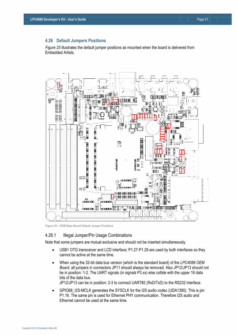
4.26 Default Jumpers Positions 41
4.26.1 Illegal Jumper/Pin Usage Combinations 41
4.27 Usage of CPU Pins 42
5 Getting Started 48
5.1 Powering 48
5.2 Demo Application 48
5.3 Installing USB Driver 50
5.4 Program Download 50
5.4.1 ISP over UART Program Download 50
5.5 Handling SO-DIMM Boards 54
5.6 Things to Note 54
5.6.1 Humming in Speaker 54
5.6.2 Current Consumption and Limits of USB Ports 55
5.6.3 LCD flickering 55
5.6.4 Initialization of External Memory Bus 56
5.6.5 USB OTG Transceiver 56
5.6.6 Rev PB1 of OEM Base Board 57
6 LCD Expansion Connector 58
7 Troubleshooting 61
7.1 Powering 61
7.2 Contact with OEM Board MCU 62
7.3 Using Test Program to Verify Correct Operation 62
8 Further Information 64
LPC4088 Developer’s Kit - User’s Guide Page 5
Copyright 2012 © Embedded Artists AB
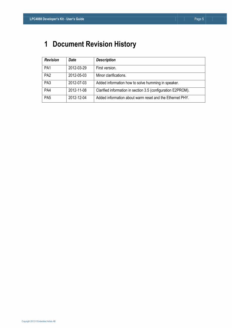
1 Document Revision History
Revision Date Description
PA1 2012-03-29 First version.
PA2 2012-05-03 Minor clarifications.
PA3 2012-07-03 Added information how to solve humming in speaker.
PA4 2012-11-08 Clarified information in section 3.5 (configuration E2PROM).
PA5 2012-12-04 Added information about warm reset and the Ethernet PHY.
LPC4088 Developer’s Kit - User’s Guide Page 6
Copyright 2012 © Embedded Artists AB
2 Introduction Thank you for buying Embedded Artists’ LPC4088 Developer’s Kit based on NXP’s ARM Cortex-M4 LPC4088 microcontroller.
This document is a User’s Guide that describes the LPC4088 OEM Board and the OEM Base Board hardware design, which together form the LPC4088 Developer’s Kit.
2.1 Features
Embedded Artists’ LPC4088 OEM Board lets you get up-and-running quickly. The small form factor OEM board offers many unique features that ease your learning curve and program development. The board has been designed for OEM applications with volume discount available.
NXP's ARM Cortex-M4 LPC4088 microcontroller in BGA package, with 512 KByte program FLASH and 96 KByte SRAM
32 MBit QSPI flash on SPIFI interface
External FLASH memories: 128 MB NAND FLASH
External data memory: 32 MB SDRAM (normally 32-bit databus width, 16-bit version exist as special order)
12.0000 MHz crystal for maximum execution speed and standard serial bit rates, including CAN and USB requirements
32.768kHz RTC crystal
100/10M Ethernet PHY/interface based on SMSC LAN8720
Buffered 32- (or 16-)bit data bus for external expansion
200 pos expansion connector (SODIMM-200 format, 0.6mm pitch)
All LPC4088 pins available (except a few used for Ethernet-PHY interface)
+3.3V only powering
Onboard reset generation
Compact SODIMM format: 68 x 50 mm
Six layer PCB design for best EMC performance
There is an accompanying OEM Base Board that can be used for initial prototyping work. The features of the board are:
Interfaces and Connectors
200 pos, 0.6mm pitch SODIMM connector for OEM Board
LCD expansion connector with control signals for touch screen interface
Expansion connector with all OEM Board signals
Ethernet connector (RJ45)
CAN interface & connector (provision for second CAN interface, but not mounted)
MMC/SD interface & connector
USB1: OTG or Host interface & connector
LPC4088 Developer’s Kit - User’s Guide Page 7
Copyright 2012 © Embedded Artists AB
USB2: Device or Host interface & connector
Provision for NXP JN5148 RF module (former Jennic) interface (RF module not included)
Full modem RS232 (cannot be fully used on 32-bit databus OEM boards)
RS422/485 interface & connector
Provision for IrDA transceiver interface (transceiver not mounted)
I2S audio codec (mic in, line in, line out, headphone out)
SWD/JTAG connector
Trace connector
Power
Power supply, either via USB or external +5V DC
Coin cell powering supported (CR1025 battery not included) for RTC and LED on ALARM output.
Other
OEM Board current measuring
Parallel NOR flash on external memory bus
16-bit register and LEDs on external memory bus
5-key joystick
3-axis accelerometer (I2C connected)
LM75 temperature sensor (I2C connected)
5 push-button keys (four via I2C and one on P2.10)
9 LEDs (8 via I2C and one on P2.10)
Analog input
USB-to-serial bridge on UART #0 (FT232R) and ISP functionality
Reset push-button and LED
Speaker output on analog output from OEM Board, or from I2S audio codec
Compact size: 160x150 mm
2.2 ESD Precaution
Please note that the LPC4088 OEM Board and OEM Base Board come without any case/box and all components are exposed for finger touches – and therefore extra attention must be paid to ESD (electrostatic discharge) precaution.
Make it a habit always to first touch the metal surface of one of the USB or Ethernet connectors for a few seconds with both hands before touching any other parts of the boards. That way, you will have the same potential as the board and therefore minimize the risk for ESD.
Never touch directly on the LPC4088 OEM Board and in general as little as possible on the OEM Base Board. The push-buttons on the OEM Base Board have grounded shields to minimize the effect of ESD.
Note that Embedded Artists does not replace boards that have been damaged by ESD.
LPC4088 Developer’s Kit - User’s Guide Page 8
Copyright 2012 © Embedded Artists AB
2.3 General Handling Care
Handle the LPC4088 OEM Board and OEM Base Board with care. The boards are not mounted in a protective case/box and are not designed for rough physical handling. Connectors can wear out after excessive use. The OEM Base Board is designed for prototyping use, and not for integration into an end-product.
For boards with LCD, do not exercise excessive pressure on the LCD glass area. That will damage the display. Also, do not apply pressure on the flex cables connecting the LCD/touch screen. These are relatively sensitive and can be damaged if too much pressure is applied to them.
Note that Embedded Artists does not replace boards where the LCD has been improperly handled.
2.4 Code Read Protection
The LPC4088 has a Code Read Protection function (specifically CRP3, see datasheet for details) that, if enabled, will make the LPC4088 impossible to reprogram (unless the user program has implemented such functionality).
Note that Embedded Artists does not replace LPC4088 OEM boards where the LPC4088 has CRP3 enabled. It’s the user’s responsibility to not invoke this mode by accident.
2.5 CE Assessment
The LPC4088 Developers Kit (consisting of the LPC4088 OEM Board and OEM Base Board) is CE marked. See separate CE Declaration of Conformity document.
The LPC4088 Developers Kit is a class A product. In a domestic environment this product may cause radio interference in which case the user may be required to take adequate measures.
EMC emission test has been performed on the LPC4088 Developers Kit. Standard interfaces like Ethernet, USB, serial have been in use. General expansion connectors where internal signals are made available (for example processor pins) have been left unconnected. Connecting other devices to the product via the general expansion connectors may alter EMC emission. It is the user’s responsibility to make sure EMC emission limits are not exceeded when connecting other devices to the general expansion connectors of the LPC4088 Developers Kit.
Due to the nature of the LPC4088 Developers Kit – an evaluation board not for integration into an end-product – fast transient immunity tests and conducted radio-frequency immunity tests have not been executed. Externally connected cables are assumed to be less than 3 meters. The general expansion connectors where internal signals are made available do not have any other ESD protection than from the chip themselves. Observe ESD precaution.
Note that the LPC4088 OEM board is classified as a component and is hence not CE marked separately. It can perform different functions in different integrations and it does not have a direct function. It is therefore not in the scope of the CE Directive. An end product, where an OEM Board is integration into, is however very likely to need CE marking.
2.6 Other Products from Embedded Artists
Embedded Artists have a broad range of LPC1000/2000/3000/4000 based boards that are very low cost and developed for prototyping / development as well as for OEM applications. Modifications for OEM applications can be done easily, even for modest production volumes. Contact Embedded Artists for further information about design and production services.
2.6.1 Design and Production Services
Embedded Artists provide design services for custom designs, either completely new or modification to existing boards. Specific peripherals and I/O can be added easily to different designs, for example, communication interfaces, specific analog or digital I/O, and power supplies. Embedded Artists has a broad, and long, experience in designing industrial electronics in general and with NXP’s
LPC4088 Developer’s Kit - User’s Guide Page 9
Copyright 2012 © Embedded Artists AB
LPC1000/2000/3000/4000 microcontroller families in specific. Our competence also includes wireless and wired communication for embedded systems. For example IEEE802.11b/g (WLAN), Bluetooth™, ZigBee™, ISM RF, Ethernet, CAN, RS485, and Fieldbuses.
2.6.2 OEM / Education / QuickStart Boards and Kits
Visit Embedded Artists’ home page, www.EmbeddedArtists.com, for information about other OEM / Education / QuickStart boards / kits or contact your local distributor.
LPC4088 Developer’s Kit - User’s Guide Page 10
Copyright 2012 © Embedded Artists AB
3 LPC4088 OEM Board Design Please read the LPC4088 OEM Board datasheet and associated schematic for information about the board. Some additional information about the LPC4088 OEM Board is presented below.
3.1 Memory Layout
The external memory controller on the LPC4088 defines eight memory regions. See table below for details about usage.
Name Control signal
Address range Memories on LPC4088 OEM Board
External memory bus comment
Static memory #0 CS0 0x8000 0000 – 0x83FF FFFF
Available for external use.
OEM Base Board can connect a parallel NOR flash to this chip select.
Static memory #1 CS1 0x9000 0000 – 0x93FF FFFF
NAND FLASH (1 GBit = 128 MByte in size)
Not available for external use. It is however possible to disable NAND flash chip by removing R57 on LPC4088 OEM Board.
Static memory #2 CS2 0x9800 0000 – 0x9BFF FFFF
Available for external use.
OEM Base Board can connect a 16-bit parallel register to this chip select.
Static memory #3 CS3 0x9C00 0000 – 0x9FFF FFFF
Available for external use.
Dynamic memory #0 DYCS0 0xA000 0000 – 0xAFFF FFFF
SDRAM (256 MBit = 32 MByte in size)
Cannot be accessed on external memory bus.
Dynamic memory #1 DYCS1 0xB000 0000 – 0xBFFF FFFF
Cannot be accessed on external memory bus.
Dynamic memory #2 DYCS2 0xC000 0000 – 0xCFFF FFFF
Cannot be accessed on external memory bus.
Dynamic memory #3 DYCS3 0xD000 0000 – 0xDFFF FFFF
Cannot be accessed on external memory bus.
As seen in the table above, it is only the static memory regions that are available on the external memory bus from the LPC4088 OEM Board. The data bus buffers on the LPC4088 OEM Board are controlled automatically and only enabled when a static memory region is accessed. The address and control bus buffers are always enabled.
Note that the BLS0, BLS1, BLS2 and BLS3 pins must be initialize for these functionalities. Else the buffer control will not work correctly.
LPC4088 Developer’s Kit - User’s Guide Page 11
Copyright 2012 © Embedded Artists AB
3.1.1 NAND Flash
Note that the NAND flash is connected after the memory bus buffers, i.e., on the same side as the LPC4088 OEM Board expansion signals. This is to allow flexibility in NAND flash usage and reduce loading on memory bus that is directly connected to the SDRAM.
The NAND FLASH has an optional busy output that can be used for controlling the erase/program operations with better precision. The signal is available on the expansion connector. If needed, the signal can be routed to a suitable (i.e., free) input pin. The OEM Base Board can connect the signal to GPIO72 by inserting a jumper between pin 3-4 on JP2. The busy status of the chip is also available under software control.
3.2 SPIFI
There is a 32 MBit QSPI flash connected to the SPIFI interface of the LPC4088.
3.3 LEDs
P2.26 and P2.27 controls two LEDs on the LPC4088 OEM Board. This control can be disabled via SJ4 (shorting pad 2-3 instead of the default 1-2). There is no real need to disable this control unless the reason is to save power. The LED driving is isolated via buffers so P2.26 and P2.27 are not loaded because of this.
3.4 Board Options
The schematic for the LPC4088 OEM Board show many options. The design has been prepared for customized versions for different needs. The board can for example be built with 16-bit databus width. The SWD/JTAG and trace connectors are not soldered by default, but can be for custom orders. It is also possible to mount a uSD memory card connector instead of the NAND flash controlled by CS1.
3.5 Configuration E2PROM
The LPC4088 OEM Board contains a configuration e2prom that can be accessed via I2C. The memory is write-protected so that the information is not deleted by accident. The memory is empty when delivered but it can be used to store information about the design revision, board configuration and Ethernet MAC address.
3.6 Migrating to LPC4088 from LPC1788
The LPC4088 is the Cortex-M4 version of LPC1788 (Cortex-M3 core). These chips are very compatible and the LPC4088 and LPC1788 OEM boards are very similar. The differences are listed below:
A 32 Mbit QSPI flash is connected to the SPIFI interface of the LPC4088. This locks usage of pins: P0.15, P0.16, P0.17, P0.18, P0.22 and P2.7.
SODIMM connector, pin 32 carries P0.10 (instead of P2.7, which is used by the SPIFI interface).
SODIMM connector, pin 57 carries P4.22 (instead of P0.10, which is used by the SPIFI interface).
SODIMM connector, pin 58 carries P4.23 (instead of P0.11, which is used by the SPIFI interface).
SODIMM connector, pin 62 carries P5.2 (instead of P0.15, which is used by the SPIFI interface).
SODIMM connector, pin 63 carries P5.3 (instead of P0.16, which is used by the SPIFI interface).
LPC4088 Developer’s Kit - User’s Guide Page 12
Copyright 2012 © Embedded Artists AB
SODIMM connector, pin 64 carries P5.1 (instead of P0.17, which is used by the SPIFI interface).
SODIMM connector, pin 65 carries P5.0 (instead of P0.18, which is used by the SPIFI interface).
The user accessible 256 Kbit I2C-E2PROM has been removed since the LCP4088 contains an on-chip E2PROM.
Pins P5.2 and P5.3 are open-drain pins (with 1.5Kohm pull-up resistors on the board).
Only minor program adjustments have to be done to handle these differences between the boards.
3.7 Migrating to LPC4088 from LPC2478
The LPC4088 can be viewed as the Cortex-M4 version of LPC2478 (ARM7TMDI core). NXP have in general made the chips very compatible. The LPC4088 is newer design and recommended for new designs. The maximum clock frequency is also higher allowing for more tasks to be handled.
Below are the things to consider when migrating to an LPC4088 OEM boards from an LPC2478 OEM board:
There is an application note from NXP describing the general issues when migrating; AN10878 Migrating to the LPC1700 series. There are both hardware and software issues to consider. It involves more than just recompiling the code. This application note is relevant also for the LPC4088 (since it builds on the LPC1788 design).
The LPC4088 OEM board is physically 2 mm higher (50mm instead of 48 mm).
The Ethernet-PHY on the LPC4088 OEM board is different (LAN8720 from SMSC instead of DP83848 from National/TI).
There are LEDs connected to pins P2.26 and P2.27 on the LPC4088 OEM board. This is normally not a problem since the LEDs can be disabled also.
There is no 32 Mbit NOR FLASH on the LPC4088 OEM board. Instead there is a 32 Mbit QSPI flash.
The LPC4088 OEM board only allows static memory region expansion, as opposed to the LPC2478 OEM board that allows both static and dynamic memory regions to be expanded on the external memory bus. This change has the benefit of simplifying
expansion of static memories, which is the most common anyways. On the LPC2478 OEM boards the databus buffers has to be controlled by an external circuit (to enable the buffers when an external memory region was accessed. With wrong control it was possible to mess up the internal databus. On the LPC4088 OEM board the databus buffers are controlled automatically on the boards. Whenever a static memory region is accessed the databus buffers are enabled.
There are a few changes in pinning, see table below. Most of the changes are related to the new port P5 of the LPC4088 and the change in external memory bus expansion (only allowing expansion of static memory regions). In most cases the LPC4088 OEM board can replace a LPC2478 OEM board without any (hardware) problems.
Pin LPC4088 OEM Board LPC2478 OEM Board Reason for change
13 NC Ethernet power down input
The new Ethernet-PHY (LAN8720) does not contain a power down input (can be
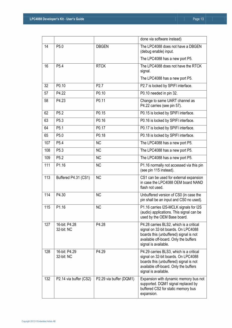
LPC4088 Developer’s Kit - User’s Guide Page 13
Copyright 2012 © Embedded Artists AB
done via software instead)
14 P5.0 DBGEN The LPC4088 does not have a DBGEN (debug enable) input.
The LPC4088 has a new port P5.
16 P5.4 RTCK The LPC4088 does not have the RTCK signal.
The LPC4088 has a new port P5.
32 P0.10 P2.7 P2.7 is locked by SPIFI interface.
57 P4.22 P0.10 P0.10 needed in pin 32.
58 P4.23 P0.11 Change to same UART channel as P4.22 carries (see pin 57).
62 P5.2 P0.15 P0.15 is locked by SPIFI interface.
63 P5.3 P0.16 P0.16 is locked by SPIFI interface.
64 P5.1 P0.17 P0.17 is locked by SPIFI interface.
65 P5.0 P0.18 P0.18 is locked by SPIFI interface.
107 P5.4 NC The LPC4088 has a new port P5.
108 P5.3 NC The LPC4088 has a new port P5.
109 P5.2 NC The LPC4088 has a new port P5.
111 P1.16 NC P1.16 normally not accessed via this pin (see pin 115 instead).
113 Buffered P4.31 (CS1) NC CS1 can be used for external expansion in case the LPC4088 OEM board NAND flash not used.
114 P4.30 NC Unbuffered version of CS0 (in case the pin shall be an input and CS0 no used).
115 P1.16 NC P1.16 carries I2S-MCLK signals for I2S (audio) applications. This signal can be used by the OEM Base board.
127 16-bit: P4.28 32-bit: NC
P4.28 P4.28 carries BLS2, which is a critical signal on 32-bit boards. On LPC4088 boards this (unbuffered) signal is not available off-board. Only the buffers signal is available.
128 16-bit: P4.29 32-bit: NC
P4.29 P4.29 carries BLS3, which is a critical signal on 32-bit boards. On LPC4088 boards this (unbuffered) signal is not available off-board. Only the buffers signal is available.
132 P2.14 via buffer (CS2) P2.29 via buffer (DQM1) Expansion with dynamic memory bus not supported. DQM1 signal replaced by buffered CS2 for static memory bus expansion.
LPC4088 Developer’s Kit - User’s Guide Page 14
Copyright 2012 © Embedded Artists AB
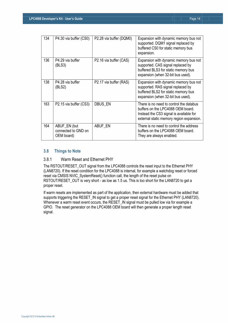
134 P4.30 via buffer (CS0) P2.28 via buffer (DQM0) Expansion with dynamic memory bus not supported. DQM1 signal replaced by buffered CS0 for static memory bus expansion.
136 P4.29 via buffer (BLS3)
P2.16 via buffer (CAS) Expansion with dynamic memory bus not supported. CAS signal replaced by buffered BLS3 for static memory bus expansion (when 32-bit bus used).
138 P4.28 via buffer (BLS2)
P2.17 via buffer (RAS) Expansion with dynamic memory bus not supported. RAS signal replaced by buffered BLS2 for static memory bus expansion (when 32-bit bus used).
163 P2.15 via buffer (CS3) DBUS_EN There is no need to control the databus buffers on the LPC4088 OEM board. Instead the CS3 signal is available for external static memory region expansion.
164 ABUF_EN (but connected to GND on OEM board)
ABUF_EN There is no need to control the address buffers on the LPC4088 OEM board. They are always enabled.
3.8 Things to Note
3.8.1 Warm Reset and Ethernet PHY
The RSTOUT/RESET_OUT signal from the LPC4088 controls the reset input to the Ethernet PHY (LAN8720). If the reset condition for the LPC4088 is internal, for example a watchdog reset or forced reset via CMSIS NVIC_SystemReset() function call, the length of the reset pulse on RSTOUT/RESET_OUT is very short - as low as 1.5 us. This is too short for the LAN8720 to get a proper reset.
If warm resets are implemented as part of the application, then external hardware must be added that supports triggering the RESET_IN signal to get a proper reset signal for the Ethernet PHY (LAN8720). Whenever a warm reset event occurs, the RESET_IN signal must be pulled low via for example a GPIO. The reset generator on the LPC4088 OEM board will then generate a proper length reset signal.
LPC4088 Developer’s Kit - User’s Guide Page 15
Copyright 2012 © Embedded Artists AB
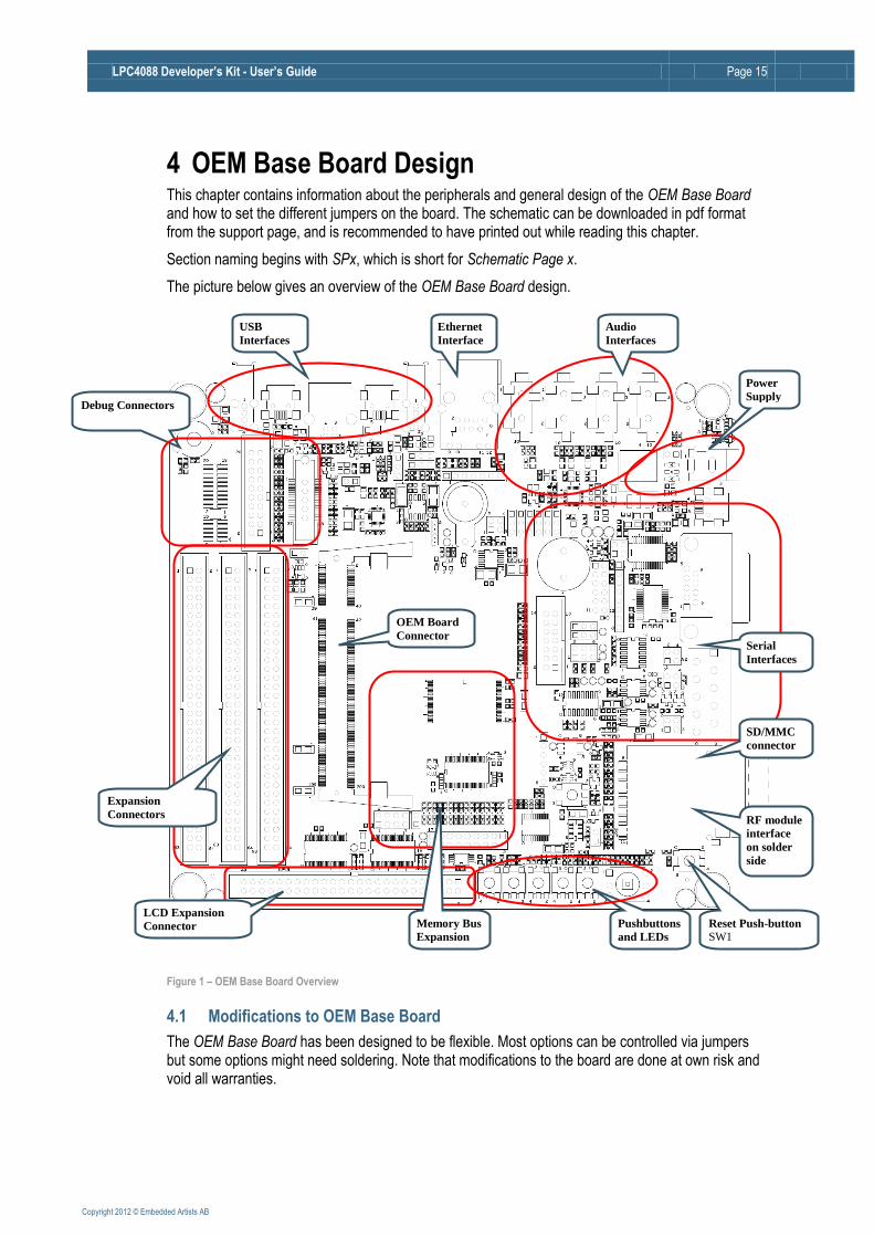
4 OEM Base Board Design This chapter contains information about the peripherals and general design of the OEM Base Board and how to set the different jumpers on the board. The schematic can be downloaded in pdf format from the support page, and is recommended to have printed out while reading this chapter.
Section naming begins with SPx, which is short for Schematic Page x.
The picture below gives an overview of the OEM Base Board design.
Figure 1 – OEM Base Board Overview
4.1 Modifications to OEM Base Board
The OEM Base Board has been designed to be flexible. Most options can be controlled via jumpers but some options might need soldering. Note that modifications to the board are done at own risk and void all warranties.
Debug Connectors
Expansion
Connectors
LCD Expansion
Connector
OEM Board
Connector Serial
Interfaces
Audio
Interfaces
USB
Interfaces
Ethernet
Interface
Power
Supply
SD/MMC
connector
Pushbuttons
and LEDs Memory Bus
Expansion
RF module
interface
on solder
side
Reset Push-button SW1
LPC4088 Developer’s Kit - User’s Guide Page 16
Copyright 2012 © Embedded Artists AB
4.2 SP2: OEM Board Connector
The LPC4088 OEM board connector is a standard DDR2 SO-DIMM socket with 200 positions and 0.6mm pitch. It has 1.8V keying (which is what DDR2 stands for). The signal names are general and represent the OEM base board functionality, rather than the LPC4088 signal names. This is because the OEM base board also supports other OEM boards.
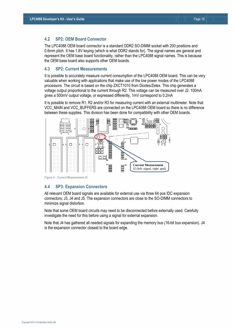
4.3 SP2: Current Measurements
It is possible to accurately measure current consumption of the LPC4088 OEM board. This can be very valuable when working with applications that make use of the low power modes of the LPC4088 processors. The circuit is based on the chip ZXCT1010 from Diodes/Zetex. This chip generates a voltage output proportional to the current through R2. This voltage can be measured over J2. 100mA gives a 500mV output voltage, or expressed differently, 1mV correspond to 0.2mA
It is possible to remove R1, R2 and/or R3 for measuring current with an external multimeter. Note that VCC_MAIN and VCC_BUFFERS are connected on the LPC4088 OEM board so there is no difference between these supplies. This division has been done for compatibility with other OEM boards.
Figure 2 – Current Measurement J2
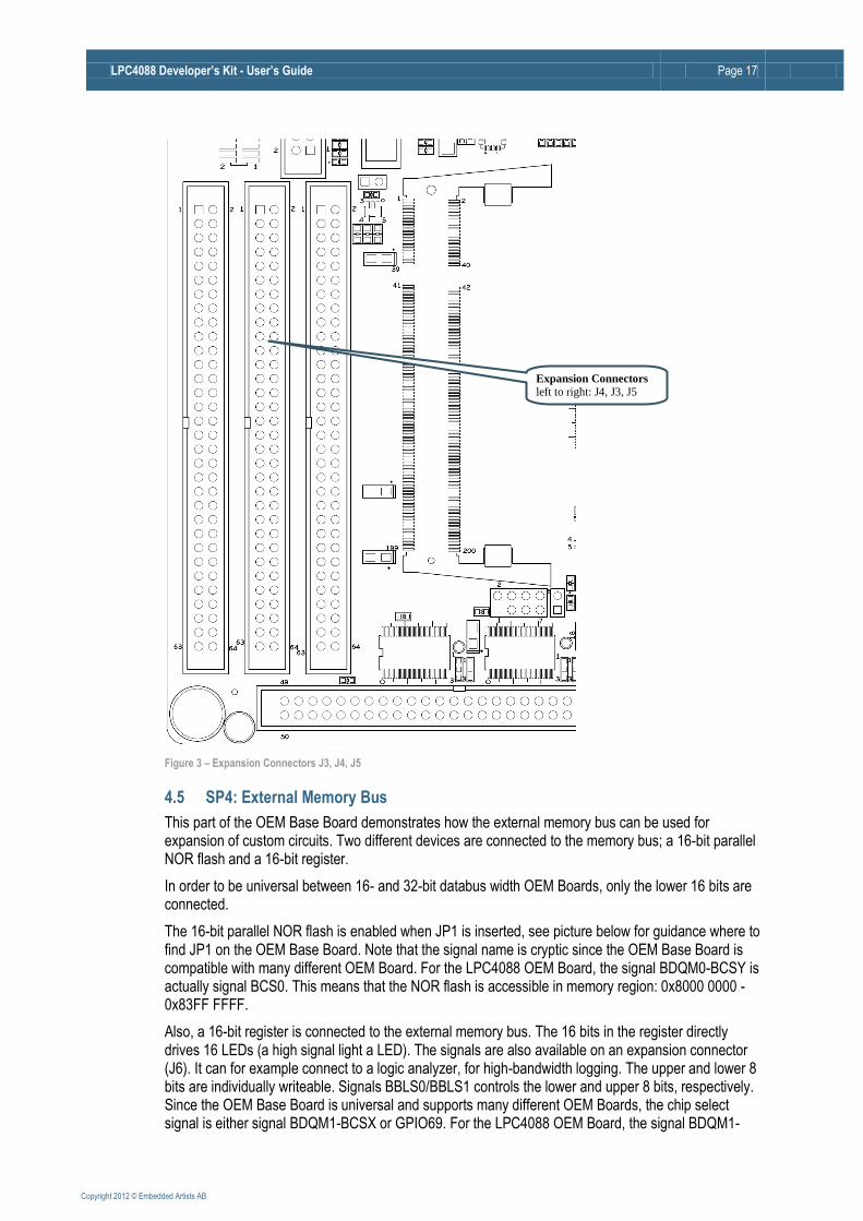
4.4 SP3: Expansion Connectors
All relevant OEM board signals are available for external use via three 64 pos IDC expansion connectors; J3, J4 and J5. The expansion connectors are close to the SO-DIMM connectors to minimize signal distortion.
Note that some OEM board circuits may need to be disconnected before externally used. Carefully investigate the need for this before using a signal for external expansion.
Note that J4 has gathered all needed signals for expanding the memory bus (16-bit bus expansion). J4 is the expansion connector closest to the board edge.
Current Measurement J2 (left: signal, right: gnd)
LPC4088 Developer’s Kit - User’s Guide Page 17
Copyright 2012 © Embedded Artists AB
Figure 3 – Expansion Connectors J3, J4, J5
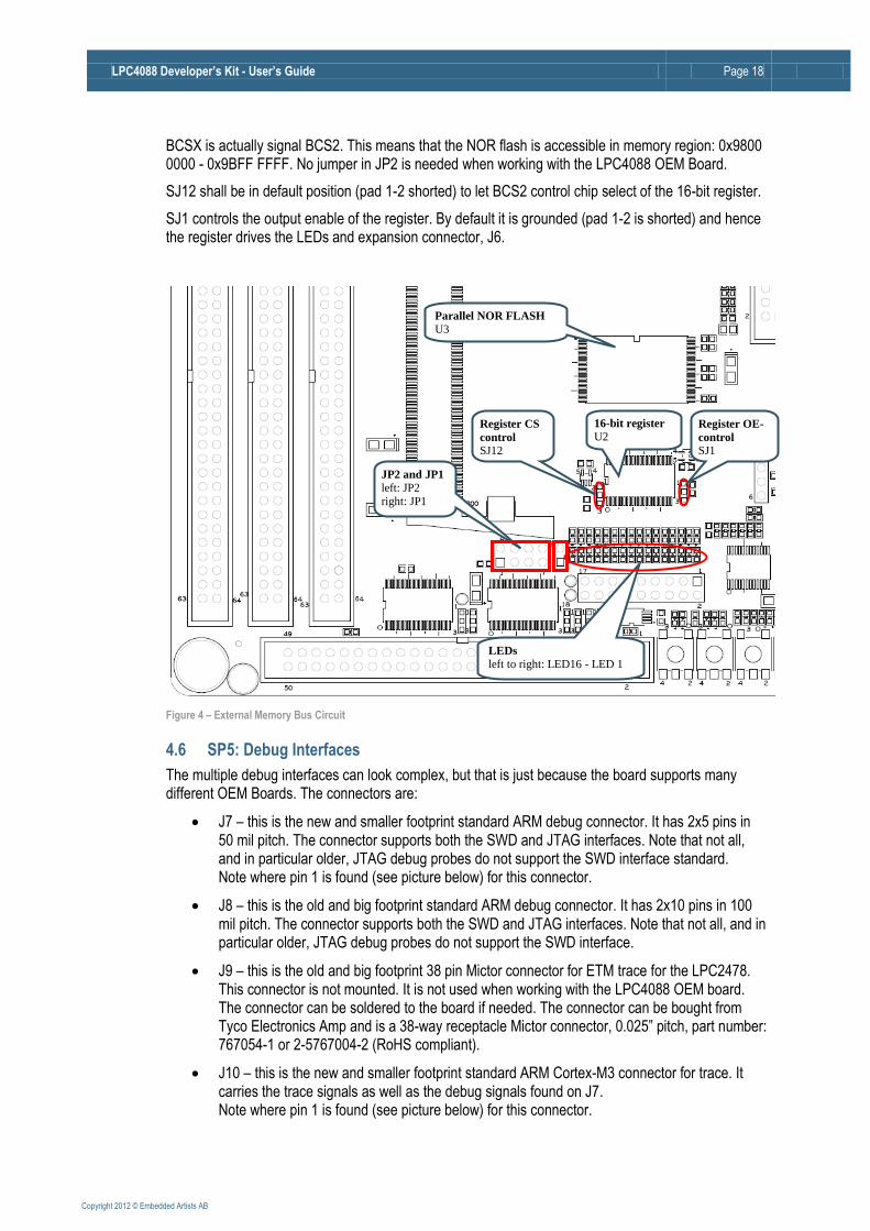
4.5 SP4: External Memory Bus
This part of the OEM Base Board demonstrates how the external memory bus can be used for expansion of custom circuits. Two different devices are connected to the memory bus; a 16-bit parallel NOR flash and a 16-bit register.
In order to be universal between 16- and 32-bit databus width OEM Boards, only the lower 16 bits are connected.
The 16-bit parallel NOR flash is enabled when JP1 is inserted, see picture below for guidance where to find JP1 on the OEM Base Board. Note that the signal name is cryptic since the OEM Base Board is compatible with many different OEM Board. For the LPC4088 OEM Board, the signal BDQM0-BCSY is actually signal BCS0. This means that the NOR flash is accessible in memory region: 0x8000 0000 - 0x83FF FFFF.
Also, a 16-bit register is connected to the external memory bus. The 16 bits in the register directly drives 16 LEDs (a high signal light a LED). The signals are also available on an expansion connector (J6). It can for example connect to a logic analyzer, for high-bandwidth logging. The upper and lower 8 bits are individually writeable. Signals BBLS0/BBLS1 controls the lower and upper 8 bits, respectively. Since the OEM Base Board is universal and supports many different OEM Boards, the chip select signal is either signal BDQM1-BCSX or GPIO69. For the LPC4088 OEM Board, the signal BDQM1-
Expansion Connectors left to right: J4, J3, J5
LPC4088 Developer’s Kit - User’s Guide Page 18
Copyright 2012 © Embedded Artists AB
BCSX is actually signal BCS2. This means that the NOR flash is accessible in memory region: 0x9800 0000 - 0x9BFF FFFF. No jumper in JP2 is needed when working with the LPC4088 OEM Board.
SJ12 shall be in default position (pad 1-2 shorted) to let BCS2 control chip select of the 16-bit register.
SJ1 controls the output enable of the register. By default it is grounded (pad 1-2 is shorted) and hence the register drives the LEDs and expansion connector, J6.
Figure 4 – External Memory Bus Circuit
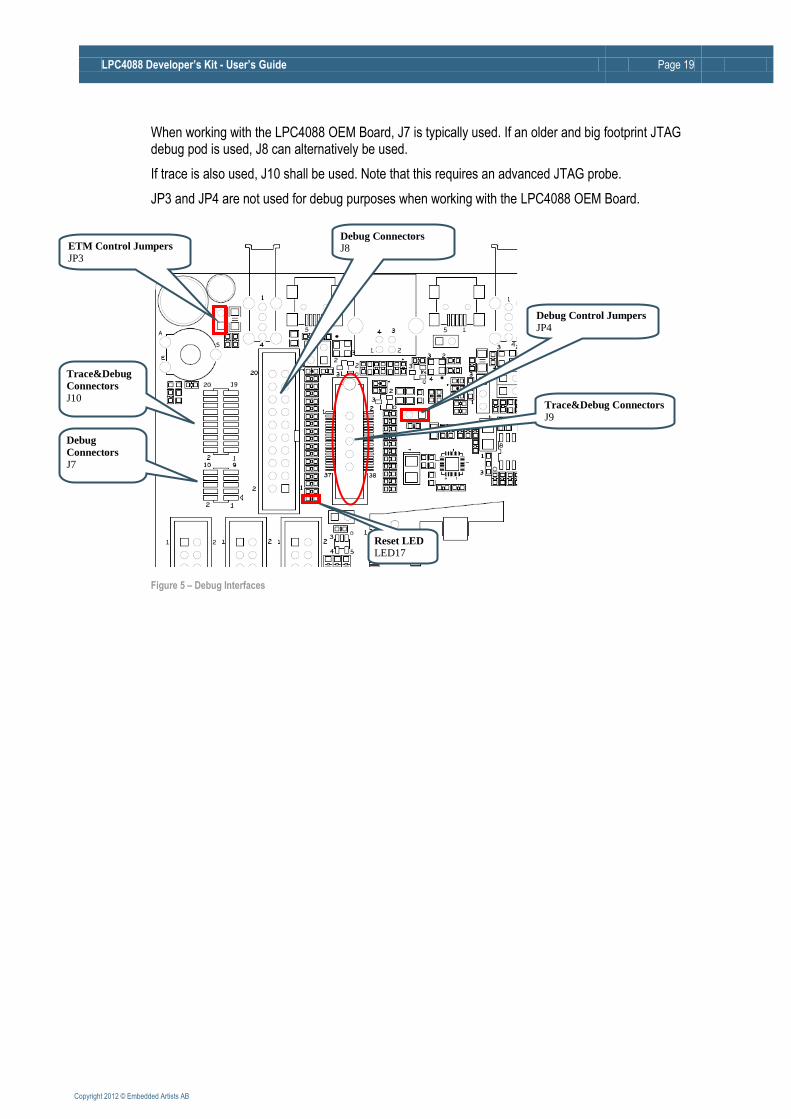
4.6 SP5: Debug Interfaces
The multiple debug interfaces can look complex, but that is just because the board supports many different OEM Boards. The connectors are:
J7 – this is the new and smaller footprint standard ARM debug connector. It has 2x5 pins in 50 mil pitch. The connector supports both the SWD and JTAG interfaces. Note that not all, and in particular older, JTAG debug probes do not support the SWD interface standard. Note where pin 1 is found (see picture below) for this connector.
J8 – this is the old and big footprint standard ARM debug connector. It has 2x10 pins in 100 mil pitch. The connector supports both the SWD and JTAG interfaces. Note that not all, and in particular older, JTAG debug probes do not support the SWD interface.
J9 – this is the old and big footprint 38 pin Mictor connector for ETM trace for the LPC2478. This connector is not mounted. It is not used when working with the LPC4088 OEM board. The connector can be soldered to the board if needed. The connector can be bought from Tyco Electronics Amp and is a 38-way receptacle Mictor connector, 0.025” pitch, part number: 767054-1 or 2-5767004-2 (RoHS compliant).
J10 – this is the new and smaller footprint standard ARM Cortex-M3 connector for trace. It carries the trace signals as well as the debug signals found on J7. Note where pin 1 is found (see picture below) for this connector.
16-bit register U2
Parallel NOR FLASH U3
JP2 and JP1 left: JP2
right: JP1
LEDs left to right: LED16 - LED 1
Register CS
control SJ12
Register OE-
control SJ1
LPC4088 Developer’s Kit - User’s Guide Page 19
Copyright 2012 © Embedded Artists AB
When working with the LPC4088 OEM Board, J7 is typically used. If an older and big footprint JTAG debug pod is used, J8 can alternatively be used.
If trace is also used, J10 shall be used. Note that this requires an advanced JTAG probe.
JP3 and JP4 are not used for debug purposes when working with the LPC4088 OEM Board.
Figure 5 – Debug Interfaces
Trace&Debug Connectors J9
Trace&Debug
Connectors J10
Debug Connectors J8
Debug
Connectors J7
ETM Control Jumpers JP3
Reset LED LED17
Debug Control Jumpers JP4
LPC4088 Developer’s Kit - User’s Guide Page 20
Copyright 2012 © Embedded Artists AB
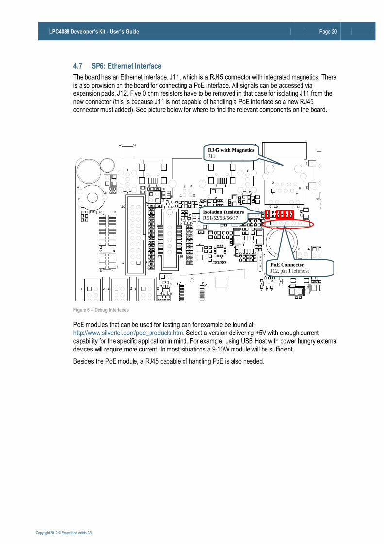
4.7 SP6: Ethernet Interface
The board has an Ethernet interface, J11, which is a RJ45 connector with integrated magnetics. There is also provision on the board for connecting a PoE interface. All signals can be accessed via expansion pads, J12. Five 0 ohm resistors have to be removed in that case for isolating J11 from the new connector (this is because J11 is not capable of handling a PoE interface so a new RJ45 connector must added). See picture below for where to find the relevant components on the board.
Figure 6 – Debug Interfaces
PoE modules that can be used for testing can for example be found at http://www.silvertel.com/poe_products.htm. Select a version delivering +5V with enough current capability for the specific application in mind. For example, using USB Host with power hungry external devices will require more current. In most situations a 9-10W module will be sufficient.
Besides the PoE module, a RJ45 capable of handling PoE is also needed.
PoE Connector J12, pin 1 leftmost
Isolation Resistors R51/52/53/56/57
RJ45 with Magnetics J11
LPC4088 Developer’s Kit - User’s Guide Page 21
Copyright 2012 © Embedded Artists AB
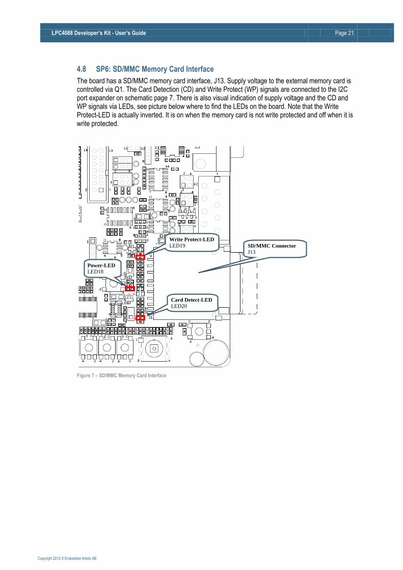
4.8 SP6: SD/MMC Memory Card Interface
The board has a SD/MMC memory card interface, J13. Supply voltage to the external memory card is controlled via Q1. The Card Detection (CD) and Write Protect (WP) signals are connected to the I2C port expander on schematic page 7. There is also visual indication of supply voltage and the CD and WP signals via LEDs, see picture below where to find the LEDs on the board. Note that the Write Protect-LED is actually inverted. It is on when the memory card is not write protected and off when it is write protected.
Figure 7 – SD/MMC Memory Card Interface
SD/MMC Connector J13
Card Detect-LED LED20
Write Protect-LED LED19
Power-LED LED18
LPC4088 Developer’s Kit - User’s Guide Page 22
Copyright 2012 © Embedded Artists AB
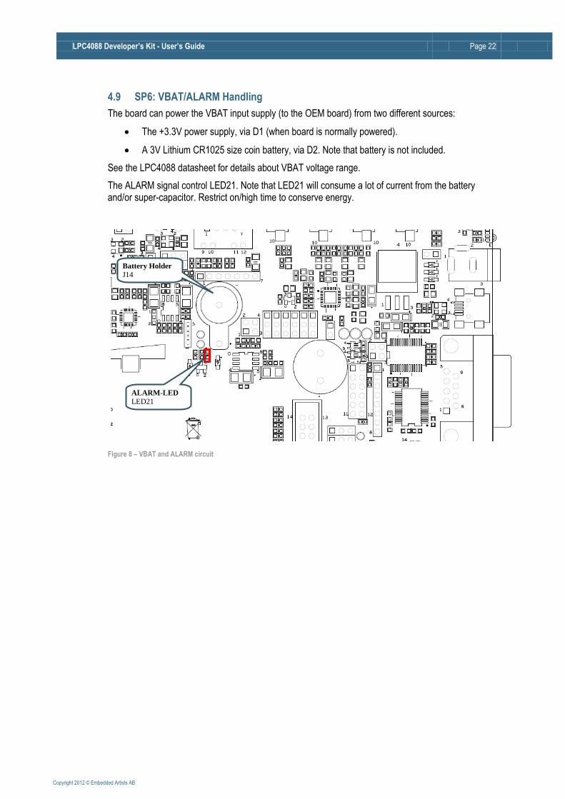
4.9 SP6: VBAT/ALARM Handling
The board can power the VBAT input supply (to the OEM board) from two different sources:
The +3.3V power supply, via D1 (when board is normally powered).
A 3V Lithium CR1025 size coin battery, via D2. Note that battery is not included.
See the LPC4088 datasheet for details about VBAT voltage range.
The ALARM signal control LED21. Note that LED21 will consume a lot of current from the battery and/or super-capacitor. Restrict on/high time to conserve energy.
Figure 8 – VBAT and ALARM circuit
ALARM-LED LED21
Battery Holder J14
LPC4088 Developer’s Kit - User’s Guide Page 23
Copyright 2012 © Embedded Artists AB
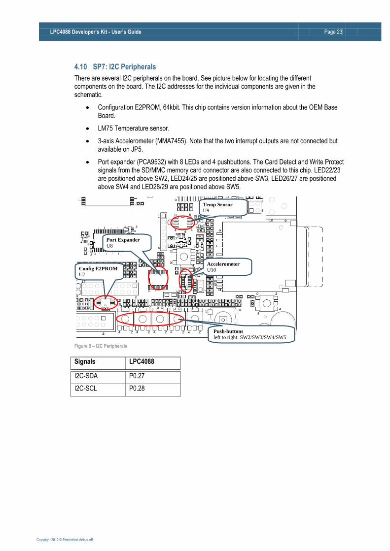
4.10 SP7: I2C Peripherals
There are several I2C peripherals on the board. See picture below for locating the different components on the board. The I2C addresses for the individual components are given in the schematic.
Configuration E2PROM, 64kbit. This chip contains version information about the OEM Base Board.
LM75 Temperature sensor.
3-axis Accelerometer (MMA7455). Note that the two interrupt outputs are not connected but available on JP5.
Port expander (PCA9532) with 8 LEDs and 4 pushbuttons. The Card Detect and Write Protect signals from the SD/MMC memory card connector are also connected to this chip. LED22/23 are positioned above SW2, LED24/25 are positioned above SW3, LED26/27 are positioned above SW4 and LED28/29 are positioned above SW5.
Figure 9 – I2C Peripherals
Signals LPC4088
I2C-SDA P0.27
I2C-SCL P0.28
Config E2PROM U7
Port Expander U8
Temp Sensor U9
Accelerometer U10
Push-buttons left to right: SW2/SW3/SW4/SW5
LPC4088 Developer’s Kit - User’s Guide Page 24
Copyright 2012 © Embedded Artists AB
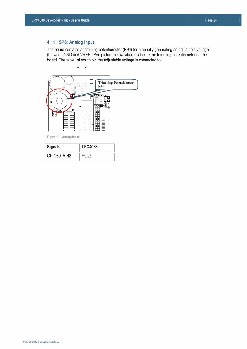
4.11 SP8: Analog Input
The board contains a trimming potentiometer (R94) for manually generating an adjustable voltage (between GND and VREF). See picture below where to locate the trimming potentiometer on the board. The table list which pin the adjustable voltage is connected to.
Figure 10 – Analog Input
Signals LPC4088
GPIO39_AIN2 P0.25
Trimming Potentiometer R94
LPC4088 Developer’s Kit - User’s Guide Page 25
Copyright 2012 © Embedded Artists AB
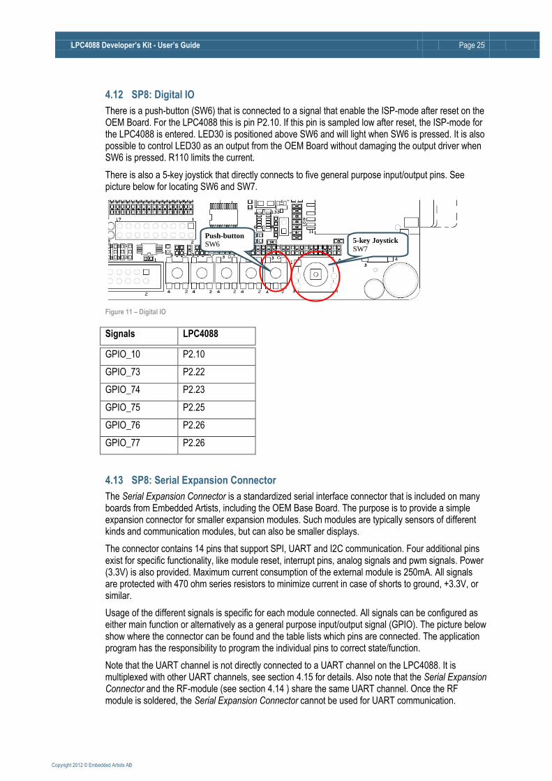
4.12 SP8: Digital IO
There is a push-button (SW6) that is connected to a signal that enable the ISP-mode after reset on the OEM Board. For the LPC4088 this is pin P2.10. If this pin is sampled low after reset, the ISP-mode for the LPC4088 is entered. LED30 is positioned above SW6 and will light when SW6 is pressed. It is also possible to control LED30 as an output from the OEM Board without damaging the output driver when SW6 is pressed. R110 limits the current.
There is also a 5-key joystick that directly connects to five general purpose input/output pins. See picture below for locating SW6 and SW7.
Figure 11 – Digital IO
Signals LPC4088
GPIO_10 P2.10
GPIO_73 P2.22
GPIO_74 P2.23
GPIO_75 P2.25
GPIO_76 P2.26
GPIO_77 P2.26
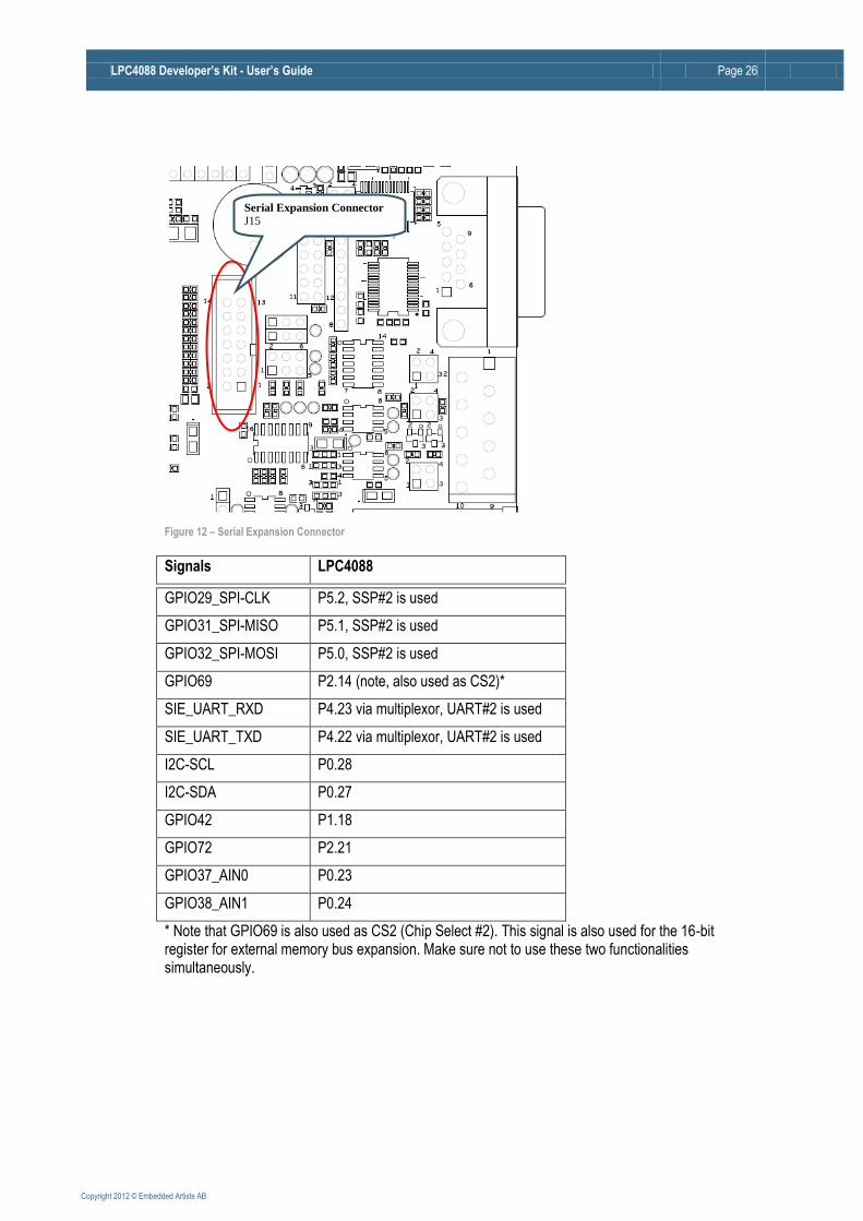
4.13 SP8: Serial Expansion Connector
The Serial Expansion Connector is a standardized serial interface connector that is included on many boards from Embedded Artists, including the OEM Base Board. The purpose is to provide a simple expansion connector for smaller expansion modules. Such modules are typically sensors of different kinds and communication modules, but can also be smaller displays.
The connector contains 14 pins that support SPI, UART and I2C communication. Four additional pins exist for specific functionality, like module reset, interrupt pins, analog signals and pwm signals. Power (3.3V) is also provided. Maximum current consumption of the external module is 250mA. All signals are protected with 470 ohm series resistors to minimize current in case of shorts to ground, +3.3V, or similar.
Usage of the different signals is specific for each module connected. All signals can be configured as either main function or alternatively as a general purpose input/output signal (GPIO). The picture below show where the connector can be found and the table lists which pins are connected. The application program has the responsibility to program the individual pins to correct state/function.
Note that the UART channel is not directly connected to a UART channel on the LPC4088. It is multiplexed with other UART channels, see section 4.15 for details. Also note that the Serial Expansion Connector and the RF-module (see section 4.14 ) share the same UART channel. Once the RF module is soldered, the Serial Expansion Connector cannot be used for UART communication.
5-key Joystick SW7
Push-button SW6
LPC4088 Developer’s Kit - User’s Guide Page 26
Copyright 2012 © Embedded Artists AB
Figure 12 – Serial Expansion Connector
Signals LPC4088
GPIO29_SPI-CLK P5.2, SSP#2 is used
GPIO31_SPI-MISO P5.1, SSP#2 is used
GPIO32_SPI-MOSI P5.0, SSP#2 is used
GPIO69 P2.14 (note, also used as CS2)*
SIE_UART_RXD P4.23 via multiplexor, UART#2 is used
SIE_UART_TXD P4.22 via multiplexor, UART#2 is used
I2C-SCL P0.28
I2C-SDA P0.27
GPIO42 P1.18
GPIO72 P2.21
GPIO37_AIN0 P0.23
GPIO38_AIN1 P0.24
* Note that GPIO69 is also used as CS2 (Chip Select #2). This signal is also used for the 16-bit register for external memory bus expansion. Make sure not to use these two functionalities simultaneously.
Serial Expansion Connector J15
LPC4088 Developer’s Kit - User’s Guide Page 27
Copyright 2012 © Embedded Artists AB
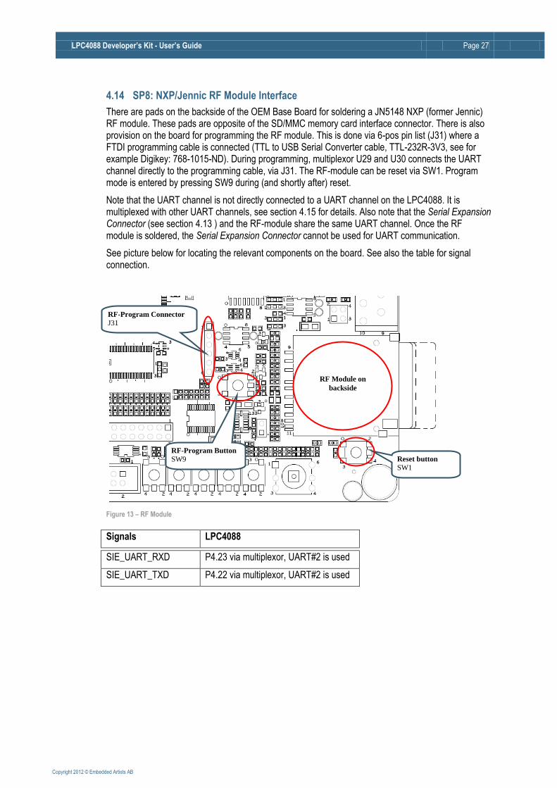
4.14 SP8: NXP/Jennic RF Module Interface
There are pads on the backside of the OEM Base Board for soldering a JN5148 NXP (former Jennic) RF module. These pads are opposite of the SD/MMC memory card interface connector. There is also provision on the board for programming the RF module. This is done via 6-pos pin list (J31) where a FTDI programming cable is connected (TTL to USB Serial Converter cable, TTL-232R-3V3, see for example Digikey: 768-1015-ND). During programming, multiplexor U29 and U30 connects the UART channel directly to the programming cable, via J31. The RF-module can be reset via SW1. Program mode is entered by pressing SW9 during (and shortly after) reset.
Note that the UART channel is not directly connected to a UART channel on the LPC4088. It is multiplexed with other UART channels, see section 4.15 for details. Also note that the Serial Expansion Connector (see section 4.13 ) and the RF-module share the same UART channel. Once the RF module is soldered, the Serial Expansion Connector cannot be used for UART communication.
See picture below for locating the relevant components on the board. See also the table for signal connection.
Figure 13 – RF Module
Signals LPC4088
SIE_UART_RXD P4.23 via multiplexor, UART#2 is used
SIE_UART_TXD P4.22 via multiplexor, UART#2 is used
RF Module on
backside
RF-Program Button SW9 Reset button
SW1
RF-Program Connector J31
LPC4088 Developer’s Kit - User’s Guide Page 28
Copyright 2012 © Embedded Artists AB
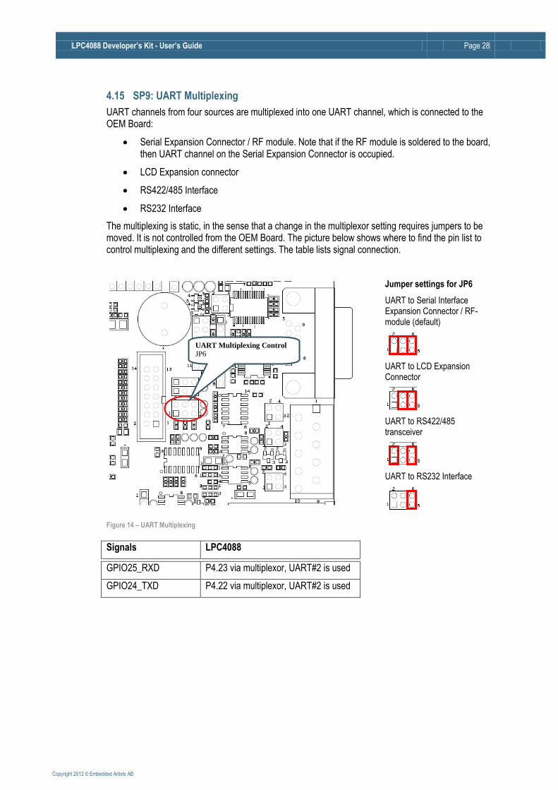
4.15 SP9: UART Multiplexing
UART channels from four sources are multiplexed into one UART channel, which is connected to the OEM Board:
Serial Expansion Connector / RF module. Note that if the RF module is soldered to the board, then UART channel on the Serial Expansion Connector is occupied.
LCD Expansion connector
RS422/485 Interface
RS232 Interface
The multiplexing is static, in the sense that a change in the multiplexor setting requires jumpers to be moved. It is not controlled from the OEM Board. The picture below shows where to find the pin list to control multiplexing and the different settings. The table lists signal connection.
Jumper settings for JP6
UART to Serial Interface Expansion Connector / RF-module (default)
UART to LCD Expansion Connector
UART to RS422/485 transceiver
UART to RS232 Interface
Figure 14 – UART Multiplexing
Signals LPC4088
GPIO25_RXD P4.23 via multiplexor, UART#2 is used
GPIO24_TXD P4.22 via multiplexor, UART#2 is used
UART Multiplexing Control JP6
LPC4088 Developer’s Kit - User’s Guide Page 29
Copyright 2012 © Embedded Artists AB
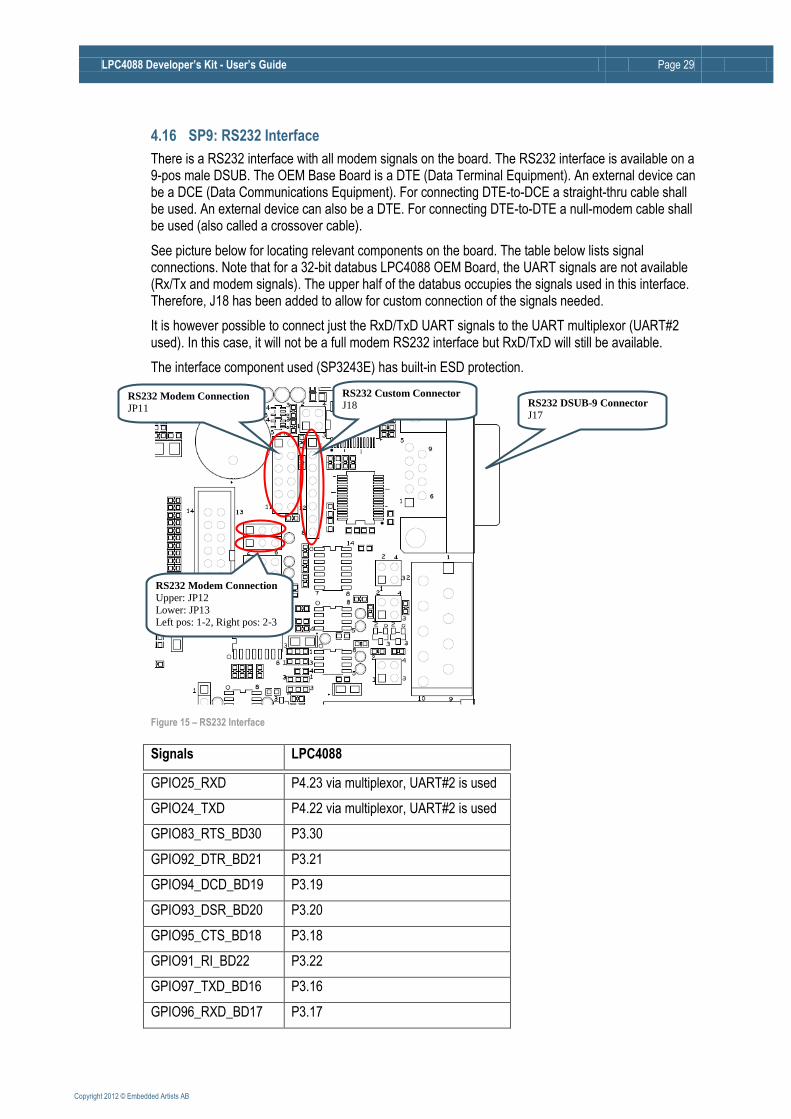
4.16 SP9: RS232 Interface
There is a RS232 interface with all modem signals on the board. The RS232 interface is available on a 9-pos male DSUB. The OEM Base Board is a DTE (Data Terminal Equipment). An external device can be a DCE (Data Communications Equipment). For connecting DTE-to-DCE a straight-thru cable shall be used. An external device can also be a DTE. For connecting DTE-to-DTE a null-modem cable shall be used (also called a crossover cable).
See picture below for locating relevant components on the board. The table below lists signal connections. Note that for a 32-bit databus LPC4088 OEM Board, the UART signals are not available (Rx/Tx and modem signals). The upper half of the databus occupies the signals used in this interface. Therefore, J18 has been added to allow for custom connection of the signals needed.
It is however possible to connect just the RxD/TxD UART signals to the UART multiplexor (UART#2 used). In this case, it will not be a full modem RS232 interface but RxD/TxD will still be available.
The interface component used (SP3243E) has built-in ESD protection.
Figure 15 – RS232 Interface
Signals LPC4088
GPIO25_RXD P4.23 via multiplexor, UART#2 is used
GPIO24_TXD P4.22 via multiplexor, UART#2 is used
GPIO83_RTS_BD30 P3.30
GPIO92_DTR_BD21 P3.21
GPIO94_DCD_BD19 P3.19
GPIO93_DSR_BD20 P3.20
GPIO95_CTS_BD18 P3.18
GPIO91_RI_BD22 P3.22
GPIO97_TXD_BD16 P3.16
GPIO96_RXD_BD17 P3.17
RS232 DSUB-9 Connector J17
RS232 Modem Connection JP11
RS232 Custom Connector J18
RS232 Modem Connection Upper: JP12
Lower: JP13 Left pos: 1-2, Right pos: 2-3
LPC4088 Developer’s Kit - User’s Guide Page 30
Copyright 2012 © Embedded Artists AB
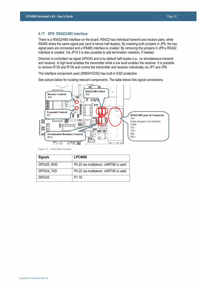
4.17 SP9: RS422/485 Interface
There is a RS422/485 interface on the board. RS422 has individual transmit and receive pairs, while RS485 share the same signal pair (and is hence half-duplex). By inserting both jumpers in JP9, the two signal pairs are connected and a RS485 interface is created. By removing the jumpers in JP9 a RS422 interface is created. Via JP10 it is also possible to add termination resistors, if needed.
Direction is controlled via signal GPIO43 and is by default half-duplex (i.e., no simultaneous transmit and receive). A high level enables the transmitter while a low level enables the receiver. It is possible to remove R135 and R136 and control the transmitter and receiver individually via JP7 and JP8.
The interface component used (SN65HVD35) has built-in ESD protection.
See picture below for locating relevant components. The table below lists signal connections.
Figure 16 – RS422/484 Interface
Signals LPC4088
GPIO25_RXD P4.23 via multiplexor, UART#2 is used
GPIO24_TXD P4.22 via multiplexor, UART#2 is used
GPIO43 P1.19
RS422/485 part of Connector J16
From top (pos 1)-to-bottom:
GND TX-
TX+
RX- RX+
RS422/485 Select JP9
Termination Resistors Control JP10
Transmit Control JP7
Receive Control
JP8
LPC4088 Developer’s Kit - User’s Guide Page 31
Copyright 2012 © Embedded Artists AB
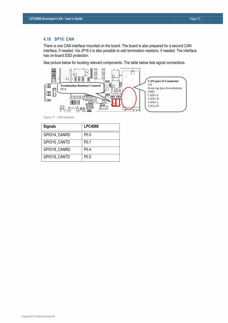
4.18 SP10: CAN
There is one CAN interface mounted on the board. The board is also prepared for a second CAN interface, if needed. Via JP16 it is also possible to add termination resistors, if needed. The interface has on-board ESD protection.
See picture below for locating relevant components. The table below lists signal connections.
Figure 17 – CAN Interface
Signals LPC4088
GPIO14_CANRD P0.0
GPIO15_CANTD P0.1
GPIO18_CANRD P0.4
GPIO19_CANTD P0.5
CAN part of Connector J16
From top (pos 6)-to-bottom: GND
CAN1-L
CAN1-H CAN2-L
CAL2-H
Termination Resistors Control JP14
LPC4088 Developer’s Kit - User’s Guide Page 32
Copyright 2012 © Embedded Artists AB
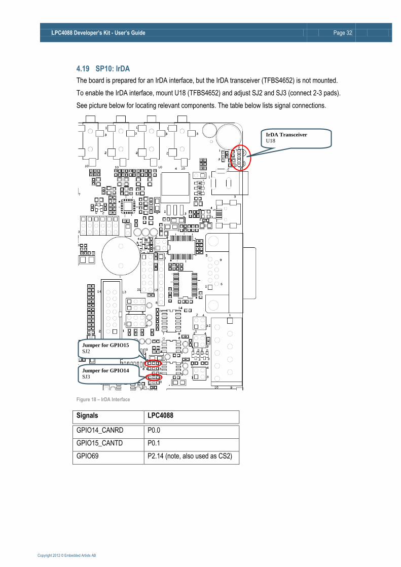
4.19 SP10: IrDA
The board is prepared for an IrDA interface, but the IrDA transceiver (TFBS4652) is not mounted.
To enable the IrDA interface, mount U18 (TFBS4652) and adjust SJ2 and SJ3 (connect 2-3 pads).
See picture below for locating relevant components. The table below lists signal connections.
Figure 18 – IrDA Interface
Signals LPC4088
GPIO14_CANRD P0.0
GPIO15_CANTD P0.1
GPIO69 P2.14 (note, also used as CS2)
IrDA Transceiver U18
Jumper for GPIO15 SJ2
Jumper for GPIO14 SJ3
LPC4088 Developer’s Kit - User’s Guide Page 33
Copyright 2012 © Embedded Artists AB
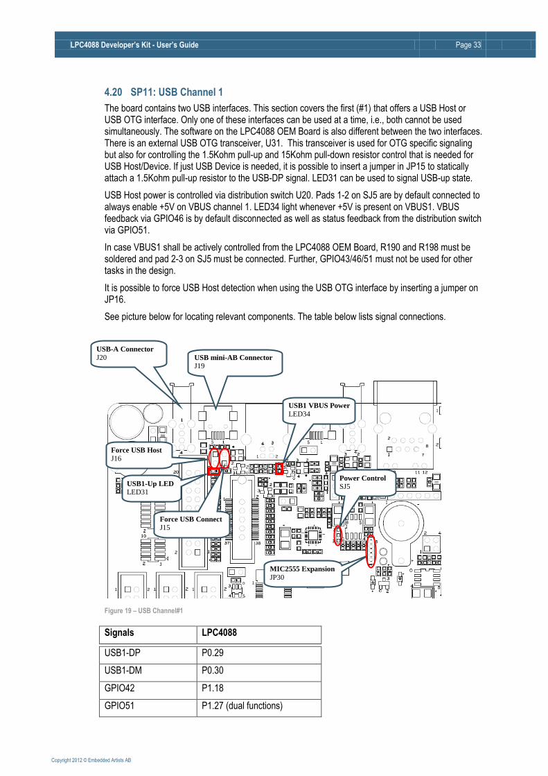
4.20 SP11: USB Channel 1
The board contains two USB interfaces. This section covers the first (#1) that offers a USB Host or USB OTG interface. Only one of these interfaces can be used at a time, i.e., both cannot be used simultaneously. The software on the LPC4088 OEM Board is also different between the two interfaces. There is an external USB OTG transceiver, U31. This transceiver is used for OTG specific signaling but also for controlling the 1.5Kohm pull-up and 15Kohm pull-down resistor control that is needed for USB Host/Device. If just USB Device is needed, it is possible to insert a jumper in JP15 to statically attach a 1.5Kohm pull-up resistor to the USB-DP signal. LED31 can be used to signal USB-up state.
USB Host power is controlled via distribution switch U20. Pads 1-2 on SJ5 are by default connected to always enable +5V on VBUS channel 1. LED34 light whenever +5V is present on VBUS1. VBUS feedback via GPIO46 is by default disconnected as well as status feedback from the distribution switch via GPIO51.
In case VBUS1 shall be actively controlled from the LPC4088 OEM Board, R190 and R198 must be soldered and pad 2-3 on SJ5 must be connected. Further, GPIO43/46/51 must not be used for other tasks in the design.
It is possible to force USB Host detection when using the USB OTG interface by inserting a jumper on JP16.
See picture below for locating relevant components. The table below lists signal connections.
Figure 19 – USB Channel#1
Signals LPC4088
USB1-DP P0.29
USB1-DM P0.30
GPIO42 P1.18
GPIO51 P1.27 (dual functions)
USB-A Connector J20 USB mini-AB Connector
J19
Force USB Host J16
Force USB Connect J15
MIC2555 Expansion JP30
Power Control SJ5 USB1-Up LED
LED31
USB1 VBUS Power LED34
LPC4088 Developer’s Kit - User’s Guide Page 34
Copyright 2012 © Embedded Artists AB
GPIO52 P1.28
GPIO53 P1.29
GPIO46 P1.22 normally not connected
GPIO43 P1.19 normally not connected
4.20.1 USB Channel 1 as USB Host
When USB channel #1 is used as USB Host, 15Kohm pull-down resistors are needed on the USB data signals. These are activated inside the USB OTG chip (U31), and this has to be done via the I2C interface of GPIO52/GPIO53.
J20 is the connector to use when USB Host is used. In order to provide +5V to the external USB device connected to this connector (J20), channel A of U20 must be enabled. It is enabled by default since SJ5 is normally connected between pin 1-2. LED34 lights green when +5V is available on J20.
JP15 shall not be inserted. JP16 has no effect.
4.20.2 USB Channel 1 as USB Device
When USB channel #1 is used as USB Device, a 1.5Kohm pull-up resistor is needed on the USB DP data signal. There are two methods to create this. JP15 is inserted and the pull-up resistor is always enabled. Alternatively, the pull-up resistor is activated inside the USB OTG chip (U31), and this has to be done via the I2C interface of GPIO52/GPIO53. In the latter case, JP15 shall not be inserted.
J19 is the connector to use when USB Device is used. Normally it should be a USB-B connector for creating a USB Device interface, but the mini-AB connector can also be used in this case. The status of VBUS can be read via U31.
JP16 shall not be inserted.
LED34 is has no meaning.
4.20.3 USB Channel 1 as USB OTG
When USB channel #1 is used as USB OTG, pull-up and pull-down resistors are controlled via the USB OTG chip (U31), and this has to be done via the I2C interface of GPIO52/GPIO53. Note that some LCD signals interfere with the I2C signals to the USB OTG chip. In particular note that R163 is typically not mounted on the OEM Base Board.
J19 is the connector to use when USB OTG is used. VBUS is controlled via U31.
JP15 shall not be inserted.
LED34 is has no meaning.
JP16 can be inserted in order to force USB Host behavior on the interface (if the external device connected to J19 cannot pull the ID signal low).
LPC4088 Developer’s Kit - User’s Guide Page 35
Copyright 2012 © Embedded Artists AB
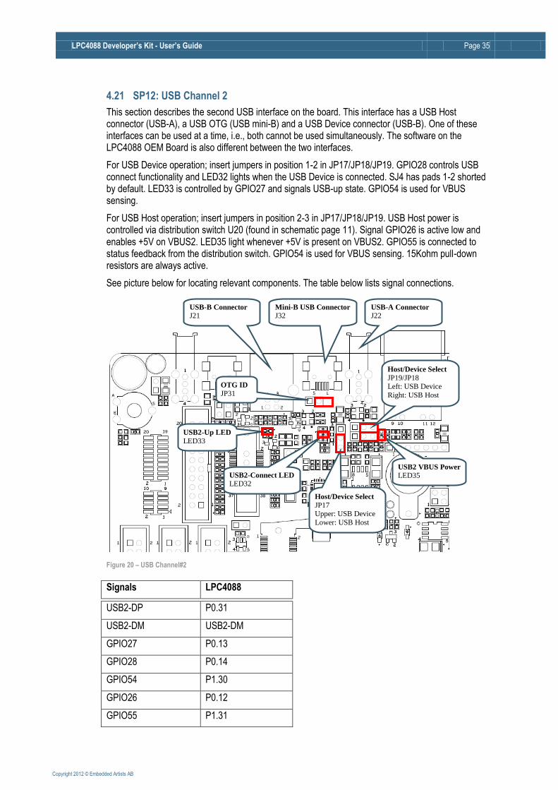
4.21 SP12: USB Channel 2
This section describes the second USB interface on the board. This interface has a USB Host connector (USB-A), a USB OTG (USB mini-B) and a USB Device connector (USB-B). One of these interfaces can be used at a time, i.e., both cannot be used simultaneously. The software on the LPC4088 OEM Board is also different between the two interfaces.
For USB Device operation; insert jumpers in position 1-2 in JP17/JP18/JP19. GPIO28 controls USB connect functionality and LED32 lights when the USB Device is connected. SJ4 has pads 1-2 shorted by default. LED33 is controlled by GPIO27 and signals USB-up state. GPIO54 is used for VBUS sensing.
For USB Host operation; insert jumpers in position 2-3 in JP17/JP18/JP19. USB Host power is controlled via distribution switch U20 (found in schematic page 11). Signal GPIO26 is active low and enables +5V on VBUS2. LED35 light whenever +5V is present on VBUS2. GPIO55 is connected to status feedback from the distribution switch. GPIO54 is used for VBUS sensing. 15Kohm pull-down resistors are always active.
See picture below for locating relevant components. The table below lists signal connections.
Figure 20 – USB Channel#2
Signals LPC4088
USB2-DP P0.31
USB2-DM USB2-DM
GPIO27 P0.13
GPIO28 P0.14
GPIO54 P1.30
GPIO26 P0.12
GPIO55 P1.31
USB-A Connector J22
USB-B Connector J21
Host/Device Select JP17 Upper: USB Device
Lower: USB Host
Host/Device Select JP19/JP18 Left: USB Device
Right: USB Host
USB2-Up LED
LED33
USB2 VBUS Power LED35 USB2-Connect LED
LED32
Mini-B USB Connector J32
OTG ID JP31
LPC4088 Developer’s Kit - User’s Guide Page 36
Copyright 2012 © Embedded Artists AB
4.21.1 USB Channel 2 as USB Host
When USB channel #2 is used as USB Host, JP17/JP18/JP19 shall all be set in position 2-3.
J22 is the connector to use when USB Host is used. In order to provide +5V to the external USB device connected to this connector (J20), channel B of U20 must be enabled. VBUS2 is enabled by GPIO26 (active low). Over-current status back is provided via GPIO55. LED35 lights green when +5V is available on J22. The VBUS2 signal is also feed back to GPIO54.
JP31 has no effect.
LED33 can signal that an external USB device has been connected.
4.21.2 USB Channel 2 as USB Device
When USB channel #2 is used as USB Device, JP17/JP18/JP19 shall all be set in position 1-2. Also a 1.5Kohm pull-up resistor is needed on the USB DP data signal. GPIO28 controls this. Alternatively, SJ4 pin 2-3 can be connected to always enable this pull-up resistor. LED32 lights when the pull-up resistor is enabled.
J22 is the connector to use when USB Device is used. This is a USB-B connector. The VBUS signal is also feed back to GPIO54.
LED35 is has no meaning.
JP31 has no effect.
4.21.3 USB Channel 2 as USB OTG
The LPC4088 does not support USB OTG directly. If this is needed, USB channel #1 must be used. This interface is provided for compatibility with other OEM boards.
The mini-AB connector can however be used instead of J22 (USB-B connector), but the interface still only supports USB Device.
LPC4088 Developer’s Kit - User’s Guide Page 37
Copyright 2012 © Embedded Artists AB
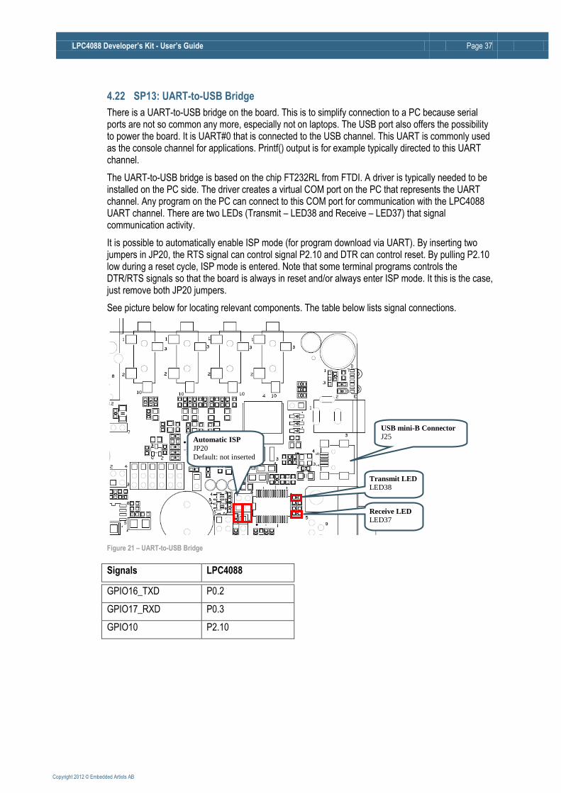
4.22 SP13: UART-to-USB Bridge
There is a UART-to-USB bridge on the board. This is to simplify connection to a PC because serial ports are not so common any more, especially not on laptops. The USB port also offers the possibility to power the board. It is UART#0 that is connected to the USB channel. This UART is commonly used as the console channel for applications. Printf() output is for example typically directed to this UART channel.
The UART-to-USB bridge is based on the chip FT232RL from FTDI. A driver is typically needed to be installed on the PC side. The driver creates a virtual COM port on the PC that represents the UART channel. Any program on the PC can connect to this COM port for communication with the LPC4088 UART channel. There are two LEDs (Transmit – LED38 and Receive – LED37) that signal communication activity.
It is possible to automatically enable ISP mode (for program download via UART). By inserting two jumpers in JP20, the RTS signal can control signal P2.10 and DTR can control reset. By pulling P2.10 low during a reset cycle, ISP mode is entered. Note that some terminal programs controls the DTR/RTS signals so that the board is always in reset and/or always enter ISP mode. It this is the case, just remove both JP20 jumpers.
See picture below for locating relevant components. The table below lists signal connections.
Figure 21 – UART-to-USB Bridge
Signals LPC4088
GPIO16_TXD P0.2
GPIO17_RXD P0.3
GPIO10 P2.10
USB mini-B Connector
J25
Transmit LED LED38
Receive LED LED37
Automatic ISP
JP20
Default: not inserted
LPC4088 Developer’s Kit - User’s Guide Page 38
Copyright 2012 © Embedded Artists AB
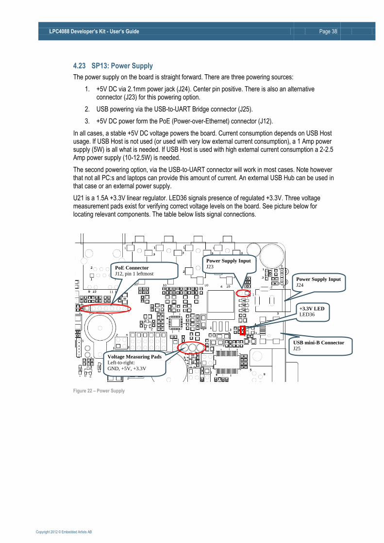
4.23 SP13: Power Supply
The power supply on the board is straight forward. There are three powering sources:
1. +5V DC via 2.1mm power jack (J24). Center pin positive. There is also an alternative connector (J23) for this powering option.
2. USB powering via the USB-to-UART Bridge connector (J25).
3. +5V DC power form the PoE (Power-over-Ethernet) connector (J12).
In all cases, a stable +5V DC voltage powers the board. Current consumption depends on USB Host usage. If USB Host is not used (or used with very low external current consumption), a 1 Amp power supply (5W) is all what is needed. If USB Host is used with high external current consumption a 2-2.5 Amp power supply (10-12.5W) is needed.
The second powering option, via the USB-to-UART connector will work in most cases. Note however that not all PC:s and laptops can provide this amount of current. An external USB Hub can be used in that case or an external power supply.
U21 is a 1.5A +3.3V linear regulator. LED36 signals presence of regulated +3.3V. Three voltage measurement pads exist for verifying correct voltage levels on the board. See picture below for locating relevant components. The table below lists signal connections.
Figure 22 – Power Supply
Voltage Measuring Pads Left-to-right:
GND, +5V, +3.3V
Power Supply Input
J24
Power Supply Input J23
+3.3V LED LED36
USB mini-B Connector
J25
PoE Connector J12, pin 1 leftmost
LPC4088 Developer’s Kit - User’s Guide Page 39
Copyright 2012 © Embedded Artists AB
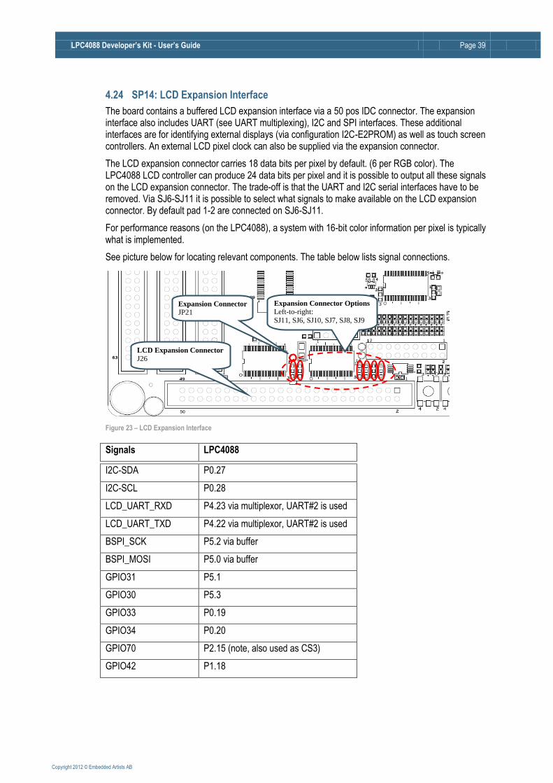
4.24 SP14: LCD Expansion Interface
The board contains a buffered LCD expansion interface via a 50 pos IDC connector. The expansion interface also includes UART (see UART multiplexing), I2C and SPI interfaces. These additional interfaces are for identifying external displays (via configuration I2C-E2PROM) as well as touch screen controllers. An external LCD pixel clock can also be supplied via the expansion connector.
The LCD expansion connector carries 18 data bits per pixel by default. (6 per RGB color). The LPC4088 LCD controller can produce 24 data bits per pixel and it is possible to output all these signals on the LCD expansion connector. The trade-off is that the UART and I2C serial interfaces have to be removed. Via SJ6-SJ11 it is possible to select what signals to make available on the LCD expansion connector. By default pad 1-2 are connected on SJ6-SJ11.
For performance reasons (on the LPC4088), a system with 16-bit color information per pixel is typically what is implemented.
See picture below for locating relevant components. The table below lists signal connections.
Figure 23 – LCD Expansion Interface
Signals LPC4088
I2C-SDA P0.27
I2C-SCL P0.28
LCD_UART_RXD P4.23 via multiplexor, UART#2 is used
LCD_UART_TXD P4.22 via multiplexor, UART#2 is used
BSPI_SCK P5.2 via buffer
BSPI_MOSI P5.0 via buffer
GPIO31 P5.1
GPIO30 P5.3
GPIO33 P0.19
GPIO34 P0.20
GPIO70 P2.15 (note, also used as CS3)
GPIO42 P1.18
LCD Expansion Connector J26
Expansion Connector Options Left-to-right:
SJ11, SJ6, SJ10, SJ7, SJ8, SJ9
Expansion Connector JP21
LPC4088 Developer’s Kit - User’s Guide Page 40
Copyright 2012 © Embedded Artists AB
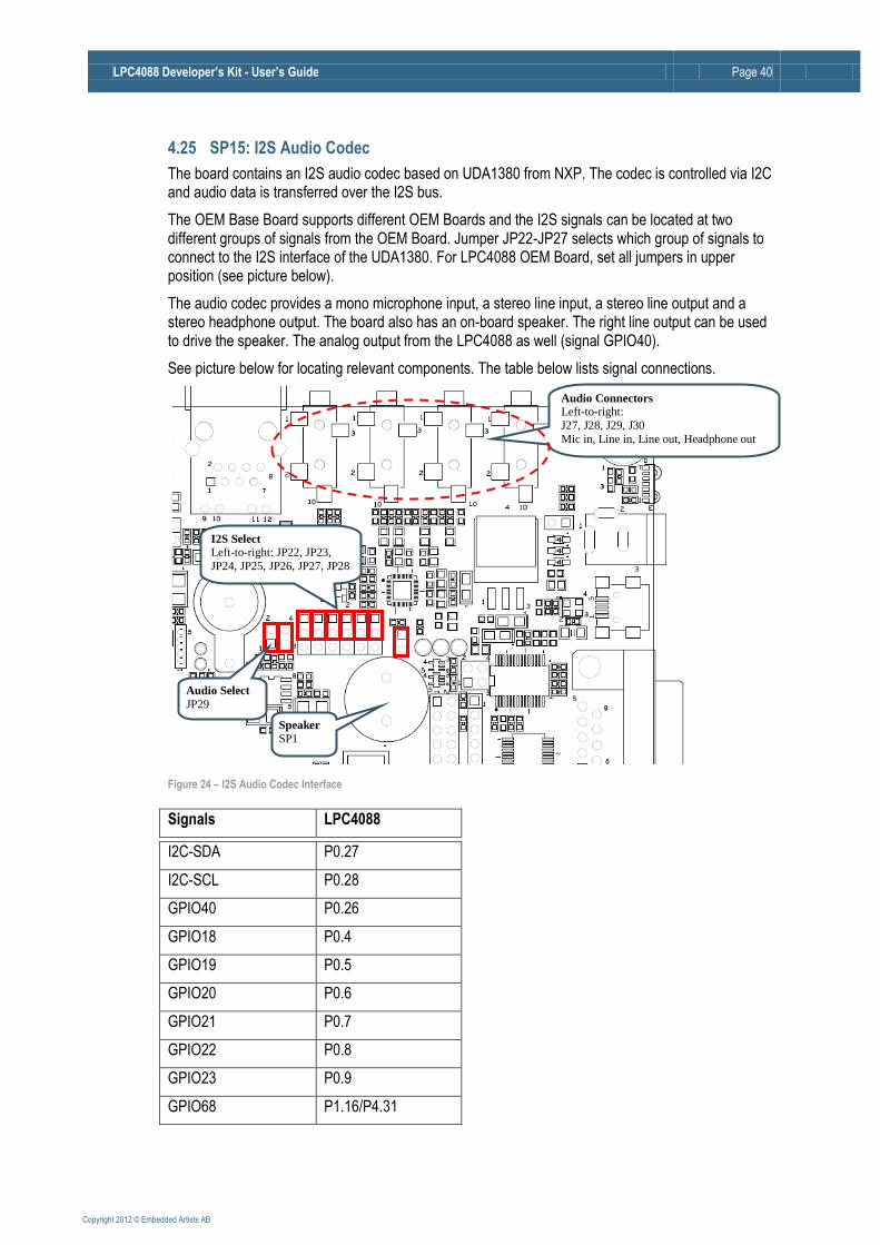
4.25 SP15: I2S Audio Codec
The board contains an I2S audio codec based on UDA1380 from NXP. The codec is controlled via I2C and audio data is transferred over the I2S bus.
The OEM Base Board supports different OEM Boards and the I2S signals can be located at two different groups of signals from the OEM Board. Jumper JP22-JP27 selects which group of signals to connect to the I2S interface of the UDA1380. For LPC4088 OEM Board, set all jumpers in upper position (see picture below).
The audio codec provides a mono microphone input, a stereo line input, a stereo line output and a stereo headphone output. The board also has an on-board speaker. The right line output can be used to drive the speaker. The analog output from the LPC4088 as well (signal GPIO40).
See picture below for locating relevant components. The table below lists signal connections.
Figure 24 – I2S Audio Codec Interface
Signals LPC4088
I2C-SDA P0.27
I2C-SCL P0.28
GPIO40 P0.26
GPIO18 P0.4
GPIO19 P0.5
GPIO20 P0.6
GPIO21 P0.7
GPIO22 P0.8
GPIO23 P0.9
GPIO68 P1.16/P4.31
Speaker SP1
Audio Connectors Left-to-right:
J27, J28, J29, J30
Mic in, Line in, Line out, Headphone out
Audio Select
JP29
I2S Select Left-to-right: JP22, JP23,
JP24, JP25, JP26, JP27, JP28
LPC4088 Developer’s Kit - User’s Guide Page 41
Copyright 2012 © Embedded Artists AB
4.26 Default Jumpers Positions
Figure 25 illustrates the default jumper positions as mounted when the board is delivered from Embedded Artists.
Figure 25 – OEM Base Board Default Jumper Positions
4.26.1 Illegal Jumper/Pin Usage Combinations
Note that some jumpers are mutual exclusive and should not be inserted simultaneously.
USB1 OTG transceiver and LCD interface; P1.27-P1.29 are used by both interfaces so they cannot be active at the same time.
When using the 32-bit data bus version (which is the standard board) of the LPC4088 OEM Board, all jumpers in connectors JP11 should always be removed. Also JP12/JP13 should not be in position: 1-2. The UART signals (in signals P3.xx) else collide with the upper 16 data bits of the data bus. JP12/JP13 can be in position: 2-3 to connect UART#2 (RxD/TxD) to the RS232 interface.
GPIO68_I2S-MCLK generates the SYSCLK for the I2S audio codec (UDA1380). This is pin P1.16. The same pin is used for Ethernet PHY communication. Therefore I2S audio and Ethernet cannot be used at the same time.
LPC4088 Developer’s Kit - User’s Guide Page 42
Copyright 2012 © Embedded Artists AB
Some signals are used on different interfaces that cannot be active simultaneous. See table in next section for information about pin usage.
4.27 Usage of CPU Pins
Almost all pins of the LPC4088 are directly available on the expansion connectors. Only in a few cases are pins used for dedicated functionality like Ethernet interface and chip select signals. Such pins are not available on the expansion connector. The table below lists all pins and their possible restrictions.
OEM Base Board signal name
LPC4088 Pin (OEM Board signal name)
Usage
GPIO0 P2.0 LCDPWR signal to LCD expansion connector.
Also connects to ETM pads, if connector mounted but not relevant for LPC4088 OEM board.
GPIO1 P2.1 LCDLE signal to LCD expansion connector.
Also connects to ETM pads, if connector mounted but not relevant for LPC4088 OEM board.
GPIO2 P2.2 LCDDCLK signal to LCD expansion connector. Connects to trace connector.
Also connects to ETM pads, if connector mounted but not relevant for LPC4088 OEM board.
GPIO3 P2.3 LCDFP signal to LCD expansion connector. Connects to trace connector.
Also connects to ETM pads, if connector mounted but not relevant for LPC4088 OEM board.
GPIO4 P2.4 LCDENAB signal to LCD expansion connector. Connects to trace connector.
Also connects to ETM pads, if connector mounted but not relevant for LPC4088 OEM board.
GPIO5 P2.5 LCDLP signal to LCD expansion connector. Connects to trace connector.
Also connects to ETM pads, if connector mounted but not relevant for LPC4088 OEM board.
GPIO6 P2.6 LCD databit 4. Connects to trace connector.
Also connects to ETM pads, if connector mounted but not relevant for LPC4088 OEM board.
GPIO7 P0.10 LCD databit 5.
Also connects to ETM pads, if connector mounted but not relevant for LPC4088 OEM board.
GPIO8 P2.8 LCD databit 6.
Also connects to ETM pads, if connector mounted but not relevant for LPC4088 OEM board.

LPC4088 Developer’s Kit - User’s Guide Page 43
Copyright 2012 © Embedded Artists AB
GPIO9 P2.9 LCD databit 7.
Also connects to ETM pads, if connector mounted but not relevant for LPC4088 OEM board.
GPIO10 P2.10 Connected to push-button (for enabling bootloader during reset or EINT0 input). Also connects to LED (active low).
Connects to USB-to-serial bridge (for automatic ISP functionality)
GPIO11 P2.11 LCDCLKIN, an external clock signal can be feed to this pin.
GPIO12 P2.12 LCD databit 18
GPIO13 P2.13 LCD databit 19
GPIO14 P0.0 Connects to RD1 for CAN channel #1, can also connect to IrDA transceiver.
GPIO15 P0.1 Connects to TD1 for CAN channel #1, can also connect to IrDA transceiver.
GPIO16 P0.2 Connects to USB-to-serial bridge (TxD on UART #0).
GPIO17 P0.3 Connects to USB-to-serial bridge (RxD on UART #0).
GPIO18 P0.4 LCD databit 0, can also be connected to RD2 for CAN channel #2
GPIO19 P0.5 LCD databit 1, can also be connected to TD2 for CAN channel #2
GPIO20 P0.6 LCD databit 8
GPIO21 P0.7 LCD databit 9
GPIO22 P0.8 LCD databit 16
GPIO23 P0.9 LCD databit 17
GPIO24 P4.22 Connects to UART multiplexing (TxD); further to LCD expansion connector, serial expansion connector, RF module, RS232 and RS422/485.
GPIO25 P4.23 Connects to UART multiplexing (RxD); further to LCD expansion connector, serial expansion connector, RF module, RS232 and RS422/485.
GPIO26 P0.12 Connects to USB2 VBUS power enable.
GPIO27 P0.13 Connects to USB2-up LED (active low).
GPIO28 P0.14 Connects to USB2-connect functionality (for USB device operation).
GPIO29 P5.2 SPI-SCK. Connects to LCD expansion connector via buffer. Connects to serial expansion connector.
GPIO30 P5.3 SPI-SSEL. Connects to LCD expansion connector.
GPIO31 P5.1 SPI-MISO. Connects to LCD expansion connector. Connects to serial expansion connector.
GPIO32 P5.0 SPI-MOSI. Connects to LCD expansion connector via buffer. Connects to serial expansion connector.
LPC4088 Developer’s Kit - User’s Guide Page 44
Copyright 2012 © Embedded Artists AB
GPIO33 P0.19 Connects to LCD expansion connector (GPIO function).
GPIO34 P0.20 Connects to LCD expansion connector (GPIO function, touch controller spi-ssel).
GPIO35 P0.21 No special usage on OEM Base Board.
GPIO36 P0.22 Is SPIFI-CLK signal on LPC4088 OEM Board.
GPIO37 P0.23 Connects to serial expansion connector.
GPIO38 P0.24 Connects to serial expansion connector.
GPIO39 P0.25 Connects to trimming potentiometer.
GPIO40 P0.26 Connects to speaker output on AOUT signal.
I2C-SDA P0.27 I2C-SDA0, connects to PCA9532, E2PROM, LM74, 3-axis Accelerometer, audio codec, serial expansion connector, lcd expansion connector.
I2C-SCL P0.28 I2C-SCL0, connects to PCA9532, E2PROM, LM74, 3-axis Accelerometer, audio codec, serial expansion connector, lcd expansion connector.
USB1-DP/DM P0.29-P0.30 Connects to USB Host/OTG interface
USB2-DP/DM P0.31, USBB-DM
Connects to USB Host/Device interface
MCICLK P1.2 Connects to MCICLK on SD/MMC connector
MCICMD P1.3 Connects to MCICMD on SD/MMC connector
MCIPWR P1.5 Connects to MCIPWR on SD/MMC connector
MCIDAT0 P1.6 Connects to MCIDAT0 on SD/MMC connector
MCIDAT1 P1.7 Connects to MCIDAT1 on SD/MMC connector
MCIDAT2 P1.11 Connects to MCIDAT2 on SD/MMC connector
MCIDAT3 P1.12 Connects to MCIDAT3 on SD/MMC connector
GPIO41 P1.13 No special usage on OEM Base Board.
GPIO42 P1.18 Connects to LCD expansion connector (backlight control). Connects to USB1-up LED (active low). Connects to serial expansion connector.
GPIO43 P1.19 Connects to RS422/485 transmit/receive control. Can optionally be connected to USB1 VBUS power enable.
GPIO44 P1.20 LCD databit 10
GPIO45 P1.21 LCD databit 11
GPIO46 P1.22 LCD databit 12 Can optionally be connected to USB1 VBUS feedback.
GPIO47 P1.23 LCD databit 13
GPIO48 P1.24 LCD databit 14
GPIO49 P1.25 LCD databit 15
GPIO50 P1.26 LCD databit 20
LPC4088 Developer’s Kit - User’s Guide Page 45
Copyright 2012 © Embedded Artists AB
GPIO51 P1.27 LCD databit 21. Also connected to USB OTG transceiver, interrupt signal. Can optionally be connected to USB1 VBUS power switch over-current flag.
GPIO52 P1.28 LCD databit 22, can also be connected to USB OTG transceiver
GPIO53 P1.29 LCD databit 23, can also be connected to USB OTG transceiver
GPIO54 P1.30 Connects to USB2 VBUS signal.
GPIO55 P1.31 Connects to USB2 VBUS power switch over-current flag.
GPIO56 NC Can be connected to I2S audio codec BCKI (I2STX-BCK) – not for LPC4088 OEM Board.
GPIO57 NC Can be connected to I2S audio codec BCKI (I2STX-DATA) – not for LPC4088 OEM Board.
GPIO58 NC Can be connected to I2S audio codec BCKI (I2STX-WS) – not for LPC4088 OEM Board.
GPIO59 NC Can be connected to I2S audio codec BCKI (I2SRX-BCK) – not for LPC4088 OEM Board.
GPIO60 P5.4 Can be connected to I2S audio codec BCKI (I2SRX-WS) – not for LPC4088 OEM Board.
GPIO61 P5.3 Same as GPIO30. Can be connected to I2S audio codec BCKI (I2SRX-DATA) – not for LPC4088 OEM Board.
GPIO62 P5.2 Same as GPIO29.
GPIO63 NC No special usage on OEM Base Board.
GPIO64 P1.16 No special usage on OEM Base Board.
GPIO65 NC No special usage on OEM Base Board.
GPIO66 BCS1 No special usage on OEM Base Board.
GPIO67 P4.30 No special usage on OEM Base Board.
GPIO68 P1.16 Can be connected to I2S audio codec SYSCLK.
GPIO69
BDQM1-BCSX
Direct: P2.14
Buffered: BCS2
CS2, chip select for 16-bit register on external memory bus.
Can be used as enable signal for IrDA transceiver (active low).
GPIO70
BCS3-DBUS_EN
Direct: P2.15
Buffered: BCS3
Connects to LCD expansion connector (interrupt signal from touch screen controller).
GPIO71 P2.19 Can be connected to Ethernet PHY interrupt output
GPIO72 P2.21 Can be connected to NAND FLASH busy output. Connects to serial expansion connector.
GPIO73 P2.22 Connects to joystick switch
GPIO74 P2.23 Connects to joystick switch
GPIO75 P2.25 Connects to joystick switch
GPIO76 P2.26 Connects to joystick switch
LPC4088 Developer’s Kit - User’s Guide Page 46
Copyright 2012 © Embedded Artists AB
GPIO77 P2.27 Connects to joystick switch
GPIO78 P2.30 No special usage on OEM Base Board.
Note that P2.30 is not available on 32-bit databus LPC4088 OEM Boards, only on 16-bit databus versions.
GPIO79 P2.31 No special usage on OEM Base Board.
Note that P2.30 is not available on 32-bit databus LPC4088 OEM Boards, only on 16-bit databus versions.
GPIO80
BBLS2
Direct: P4.28
Buffered: BBLS2
LCD databit 2.
Note that direct P4.28 is not available on 32-bit databus LPC4088 OEM Boards, only on 16-bit databus versions.
GPIO81
BBLS3
Direct: P4.29
Buffered: BBLS3
LCD databit 3
Note that direct P4.29 is not available on 32-bit databus LPC4088 OEM Boards, only on 16-bit databus versions.
BD0-BD15 P3.0-P3.15 Occupied for 16-bit databus versions. Connects to parallel NOR flash and 16-bit register.
BD16-DB31 P3.16-P3.31 Also occupied for 32-bit databus versions.
No special usage on OEM Base Board.
GPIO97 P3.16 Can be connected to RS232 interface (if 16-bit databus version used)
GPIO96 P3.17 Can be connected to RS232 interface (if 16-bit databus version used)
GPIO95 P3.18 Can be connected to RS232 interface (if 16-bit databus version used)
GPIO94 P3.19 Can be connected to RS232 interface (if 16-bit databus version used)
GPIO93 P3.20 Can be connected to RS232 interface (if 16-bit databus version used)
GPIO92 P3.21 Can be connected to RS232 interface (if 16-bit databus version used)
GPIO91 P3.22 Can be connected to RS232 interface (if 16-bit databus version used)
GPIO90 P3.23 No special usage on QVGA Base Board (if 16-bit databus version used)
GPIO89 P3.24 No special usage on QVGA Base Board (if 16-bit databus version used)
GPIO88 P3.25 No special usage on QVGA Base Board (if 16-bit databus version used)
GPIO87 P3.26 No special usage on QVGA Base Board (if 16-bit databus version used)
GPIO86 P3.27 No special usage on QVGA Base Board (if 16-bit databus version used)
LPC4088 Developer’s Kit - User’s Guide Page 47
Copyright 2012 © Embedded Artists AB
GPIO85 P3.28 No special usage on QVGA Base Board (if 16-bit databus version used)
GPIO84 P3.29 No special usage on QVGA Base Board (if 16-bit databus version used)
GPIO83 P3.30 Can be connected to RS232 interface (if 16-bit databus version used)
GPIO82 P3.31 No special usage on QVGA Base Board (if 16-bit databus version used)
BA0-BA23 P4.0-P4.23 The address bus, buffered signals from OEM Board. Connects
to parallel NOR flash and 16-bit register.
BOE P4.24 OE, buffered signal from cpu board . Connects to parallel NOR flash.
BWE P4.25 WE, buffered signal from cpu board. Connects to parallel NOR flash and 16-bit register.
BBLS0 Buffered P4.26 BLS0 controls lower 8 bits of external memory databus (16-bit parallel register). Connects to 16-bit register.
BBLS1 Buffered P4.27 BLS1 controls upper 8 bits of external memory databus (16-bit parallel register). Connects to 16-bit register.
P4.30
BDQM0-BCSY
Direct: P4.30
Buffered: BCS0
CS0, chip select for parallel NOR flash.
BCS1 Buffered P4.31 No special usage on OEM Base Board.
VBAT VBAT Super-capacitor on vbat signal
ALARM ALARM Connected to alarm-LED (active high)
VREF VREF Can be connected VDDA(V3A)
VDDA, VSSA
VDDA, VSSA
Used to generate reference voltage for trimpot (analog inputs)
SWD/JTAG signals
SWD/JTAG signals
Connected to SWD/JTAG connectors
JTAG_DBGEN P5.0 JP4 can pull signal high.
RESET RESET Connects to RESET push-button and USB-to-serial bridge (for
automatic ISP functionality)
RSTOUT RSTOUT Connects to RESET LED indicator.
Used to reset PCA9532, UDA1380, FT232RL, MIC2555, RF module and LCD expansion connector.
LPC4088 Developer’s Kit - User’s Guide Page 48
Copyright 2012 © Embedded Artists AB
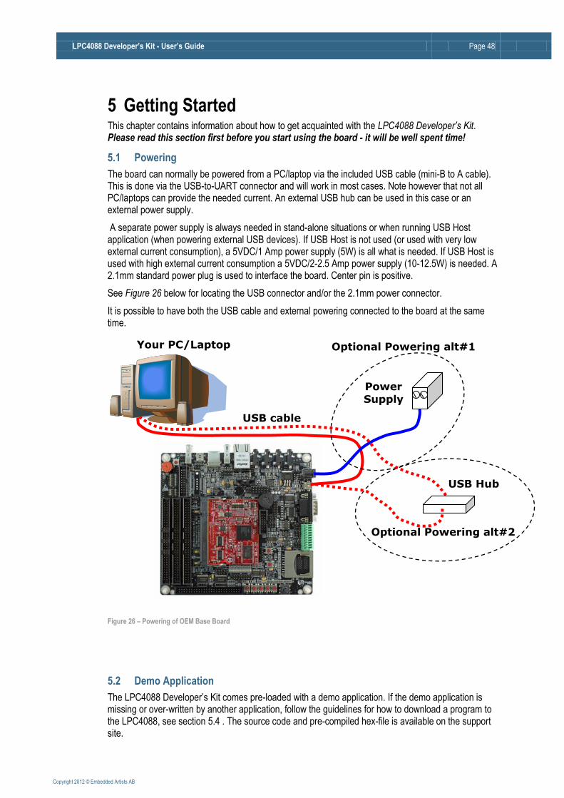
5 Getting Started This chapter contains information about how to get acquainted with the LPC4088 Developer’s Kit. Please read this section first before you start using the board - it will be well spent time!
5.1 Powering
The board can normally be powered from a PC/laptop via the included USB cable (mini-B to A cable). This is done via the USB-to-UART connector and will work in most cases. Note however that not all PC/laptops can provide the needed current. An external USB hub can be used in this case or an external power supply.
A separate power supply is always needed in stand-alone situations or when running USB Host application (when powering external USB devices). If USB Host is not used (or used with very low external current consumption), a 5VDC/1 Amp power supply (5W) is all what is needed. If USB Host is used with high external current consumption a 5VDC/2-2.5 Amp power supply (10-12.5W) is needed. A 2.1mm standard power plug is used to interface the board. Center pin is positive.
See Figure 26 below for locating the USB connector and/or the 2.1mm power connector.
It is possible to have both the USB cable and external powering connected to the board at the same time.
Figure 26 – Powering of OEM Base Board
5.2 Demo Application
The LPC4088 Developer’s Kit comes pre-loaded with a demo application. If the demo application is missing or over-written by another application, follow the guidelines for how to download a program to the LPC4088, see section 5.4 . The source code and pre-compiled hex-file is available on the support site.
Power Supply
Your PC/Laptop
USB cable
Optional Powering alt#1
USB Hub
Optional Powering alt#2
LPC4088 Developer’s Kit - User’s Guide Page 49
Copyright 2012 © Embedded Artists AB
The demo application demonstrates some features of the LPC4088 Developer’s Kit:
The accelerometer and memory mapped register; the row of LEDs (LED16 to LED1) are controlled by tilting the board.
Buttons and PCA9532 port expander; there is a running-light pattern on the 8 LEDs controlled by the I2C port expander. By pressing the push-buttons (also on the I2C port expander) the pattern can be changed.
Joystick and GPIO; the 5-key joystick can also control the running-lights pattern. UP-key increases the speed, CENTER-key returns it to normal and DOWN-key decreases the speed. LEFT-key changes to the previous pattern for the running lights and RIGHT-key changes to the next pattern.
Speaker and DAC; the melody played at startup demonstrates the use of DAC and DMA to output a sinus wave at different frequencies.
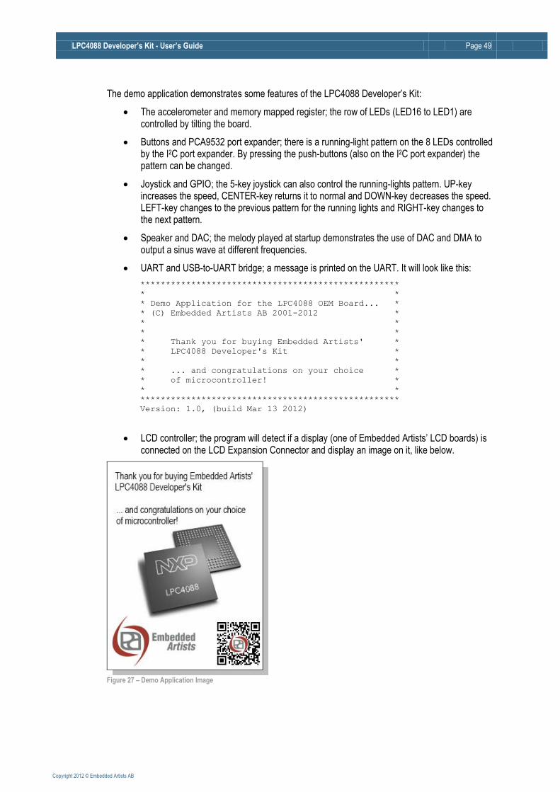
UART and USB-to-UART bridge; a message is printed on the UART. It will look like this:
***************************************************
* *
* Demo Application for the LPC4088 OEM Board... *
* (C) Embedded Artists AB 2001-2012 *
* *
* *
* Thank you for buying Embedded Artists' *
* LPC4088 Developer's Kit *
* *
* ... and congratulations on your choice *
* of microcontroller! *
* *
***************************************************
Version: 1.0, (build Mar 13 2012)
LCD controller; the program will detect if a display (one of Embedded Artists’ LCD boards) is connected on the LCD Expansion Connector and display an image on it, like below.
Figure 27 – Demo Application Image
LPC4088 Developer’s Kit - User’s Guide Page 50
Copyright 2012 © Embedded Artists AB
5.3 Installing USB Driver
The OEM Base Board contains an USB-to-UART bridge chip (FT232R from FTDI) that connects UART channel #0 on the LPC4088 to a virtual COM port on the PC/laptop (via USB). This UART channel is typically used as the console channel for applications. Printf() output can for example be directed to this UART channel.
A USB driver must be installed on the PC/laptop in order for the virtual COM port to be created. See FTDI’s installation guides for details how to install the driver for different operating systems:
http://www.ftdichip.com/Support/Documents/InstallGuides.htm
5.4 Program Download
This section describes some basic methods for downloading application code to the LPC4088. Note that this section does not describe how to create the application code (write the program and compile it). It is assumed that a binary file exist that represent the application program. This file is often a so called hex-file, which is a file format that Intel created a long time ago. It can also be a pure binary file (also call bin-file).
There are three basic methods for program download:
- ISP over UART ISP is short for In-System Programming. The LPC4088 contains a bootloader in ROM that can be enabled by pulling pin P2.10 low during reset. The application can then be downloaded over UART#0 (serial channel). An application is needed on the PC for downloading the application code.
- IAP over Ethernet or USB IAP is short for In-Application Programming. In this case, the LPC4088 flash must have a small bootloader installed that allow application code to be downloaded over Ethernet, USB or some other communication channel. The bootloader must be created by the user and is typically specific for the application. NXP has published some application notes related to this.
- SWD/JTAG There are many different SWD/JTAG interfaces on the market. NXP has created LPC-LINK. Keil has ULINK. IAR/Segger has JLINK. Code Red has Red Probe, etc. There is also OpenOCD, which is an open source project. Consult the respective manual for the SWD/JTAG interface used to get instructions how to download a hex/binary file via SWD/JTAG.
The application code is typically downloaded to the internal flash of the LPC4088 but it is not the only way. An application can also be downloaded to the internal ram of the LPC4088. Application code can also be downloaded into external memories (outside of the LPC4088). In these cases, a bootloader that supports this must be used.
Embedded Artists support site contains sample applications for the LPC4088 Developer’s Kit. Source code and pre-compiled binary images (hex-files) can be downloaded from there.
5.4.1 ISP over UART Program Download
There are two jumpers on the OEM Base Board related to the USB-to-UART serial channel control signals and automatic ISP functionality. See Figure 28 for details about where the jumpers are located. Normally the two jumpers in JP20 shall not be inserted, i.e., open. If inserted, there is a risk that the terminal program on the PC/laptop resets the board and/or enable ISP mode by accident.
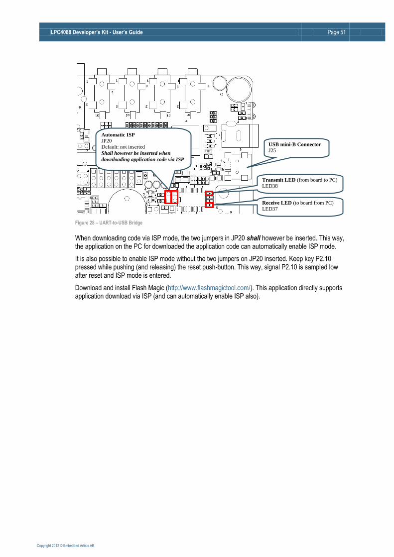
LPC4088 Developer’s Kit - User’s Guide Page 51
Copyright 2012 © Embedded Artists AB
Figure 28 – UART-to-USB Bridge
When downloading code via ISP mode, the two jumpers in JP20 shall however be inserted. This way, the application on the PC for downloaded the application code can automatically enable ISP mode.
It is also possible to enable ISP mode without the two jumpers on JP20 inserted. Keep key P2.10 pressed while pushing (and releasing) the reset push-button. This way, signal P2.10 is sampled low after reset and ISP mode is entered.
Download and install Flash Magic (http://www.flashmagictool.com/). This application directly supports application download via ISP (and can automatically enable ISP also).
USB mini-B Connector
J25
Transmit LED (from board to PC)
LED38
Receive LED (to board from PC) LED37
Automatic ISP JP20 Default: not inserted
Shall however be inserted when
downloading application code via ISP
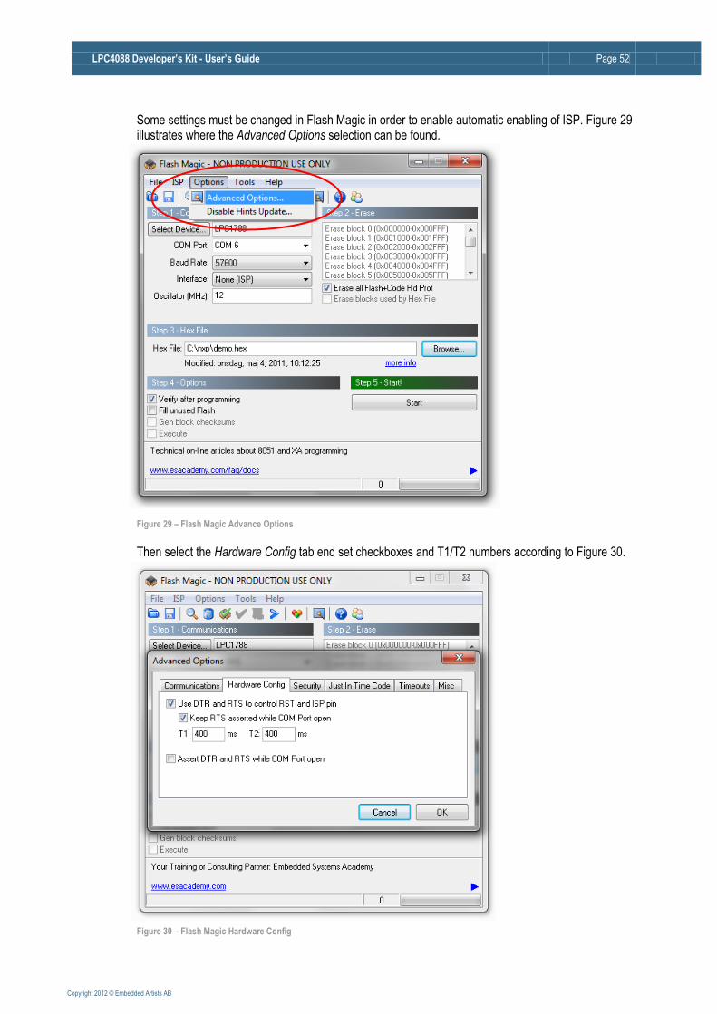
LPC4088 Developer’s Kit - User’s Guide Page 52
Copyright 2012 © Embedded Artists AB
Some settings must be changed in Flash Magic in order to enable automatic enabling of ISP. Figure 29 illustrates where the Advanced Options selection can be found.
Figure 29 – Flash Magic Advance Options
Then select the Hardware Config tab end set checkboxes and T1/T2 numbers according to Figure 30.
Figure 30 – Flash Magic Hardware Config
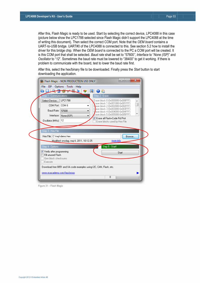
LPC4088 Developer’s Kit - User’s Guide Page 53
Copyright 2012 © Embedded Artists AB
After this, Flash Magic is ready to be used. Start by selecting the correct device, LPC4088 in this case (picture below show the LPC1788 selected since Flash Magic didn’t support the LPC4088 at the time of writing this document). Then select the correct COM port. Note that the OEM board contains a UART-to-USB bridge. UART#0 of the LPC4088 is connected to this. See section 5.2 how to install the driver for this bridge chip. When the OEM board is connected to the PC a COM port will be created. It is this COM port that shall be selected. Baud rate shall be set to “57600”, Interface to “None (ISP)” and Oscillator to “12”. Sometimes the baud rate must be lowered to “38400” to get it working. If there is problem to communicate with the board, test to lower the baud rate first.
After this, select the hex/binary file to be downloaded. Finally press the Start button to start downloading the application.
Figure 31 – Flash Magic
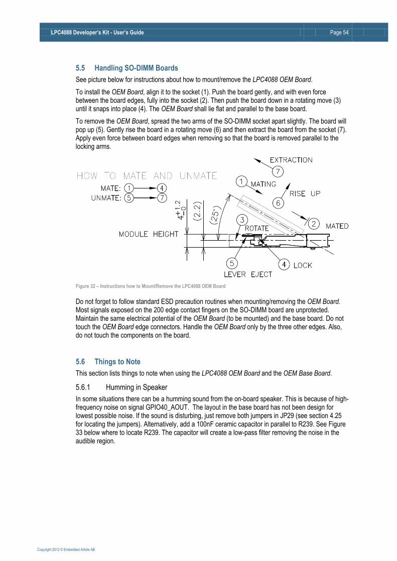
LPC4088 Developer’s Kit - User’s Guide Page 54
Copyright 2012 © Embedded Artists AB
5.5 Handling SO-DIMM Boards
See picture below for instructions about how to mount/remove the LPC4088 OEM Board.
To install the OEM Board, align it to the socket (1). Push the board gently, and with even force between the board edges, fully into the socket (2). Then push the board down in a rotating move (3) until it snaps into place (4). The OEM Board shall lie flat and parallel to the base board.
To remove the OEM Board, spread the two arms of the SO-DIMM socket apart slightly. The board will pop up (5). Gently rise the board in a rotating move (6) and then extract the board from the socket (7). Apply even force between board edges when removing so that the board is removed parallel to the locking arms.
Figure 32 – Instructions how to Mount/Remove the LPC4088 OEM Board
Do not forget to follow standard ESD precaution routines when mounting/removing the OEM Board. Most signals exposed on the 200 edge contact fingers on the SO-DIMM board are unprotected. Maintain the same electrical potential of the OEM Board (to be mounted) and the base board. Do not touch the OEM Board edge connectors. Handle the OEM Board only by the three other edges. Also, do not touch the components on the board.
5.6 Things to Note
This section lists things to note when using the LPC4088 OEM Board and the OEM Base Board.
5.6.1 Humming in Speaker
In some situations there can be a humming sound from the on-board speaker. This is because of high-frequency noise on signal GPIO40_AOUT. The layout in the base board has not been design for lowest possible noise. If the sound is disturbing, just remove both jumpers in JP29 (see section 4.25 for locating the jumpers). Alternatively, add a 100nF ceramic capacitor in parallel to R239. See Figure 33 below where to locate R239. The capacitor will create a low-pass filter removing the noise in the audible region.
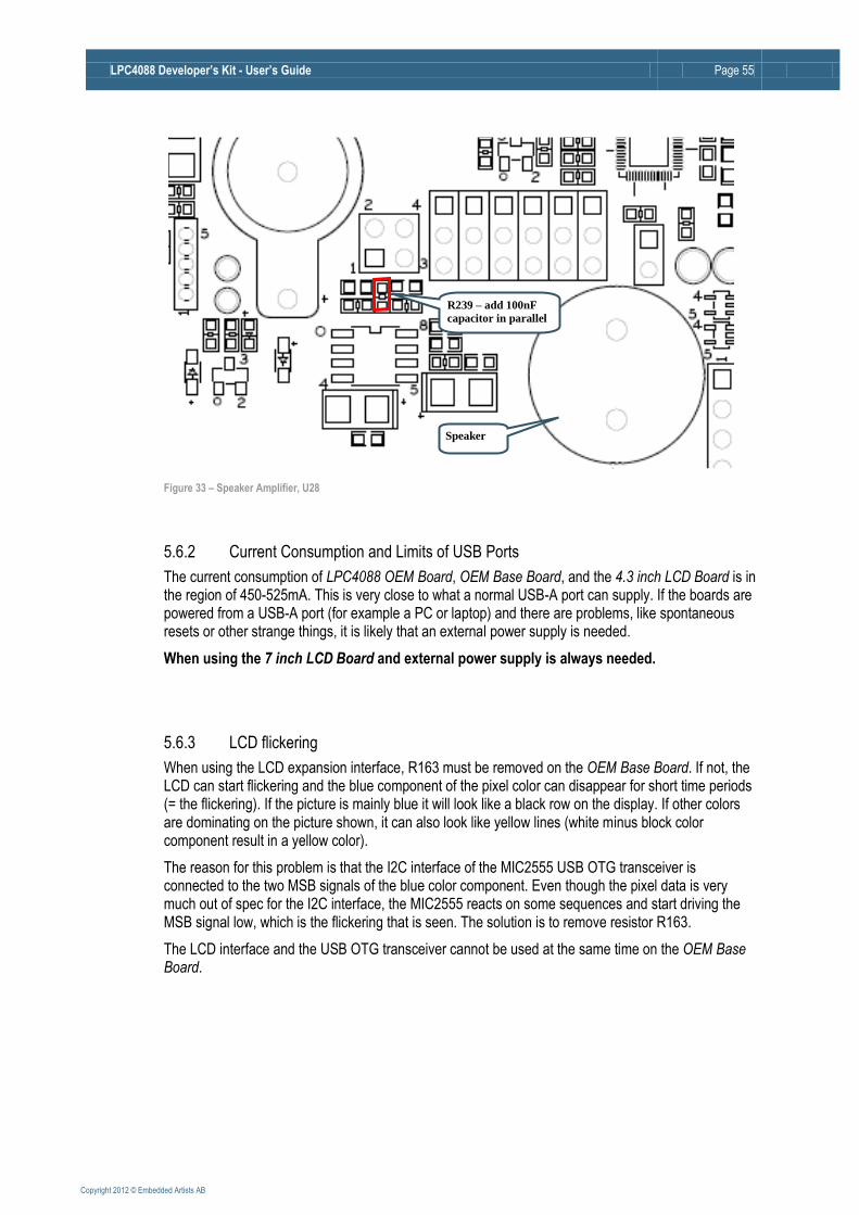
LPC4088 Developer’s Kit - User’s Guide Page 55
Copyright 2012 © Embedded Artists AB
Figure 33 – Speaker Amplifier, U28
5.6.2 Current Consumption and Limits of USB Ports
The current consumption of LPC4088 OEM Board, OEM Base Board, and the 4.3 inch LCD Board is in the region of 450-525mA. This is very close to what a normal USB-A port can supply. If the boards are powered from a USB-A port (for example a PC or laptop) and there are problems, like spontaneous resets or other strange things, it is likely that an external power supply is needed.
When using the 7 inch LCD Board and external power supply is always needed.
5.6.3 LCD flickering
When using the LCD expansion interface, R163 must be removed on the OEM Base Board. If not, the LCD can start flickering and the blue component of the pixel color can disappear for short time periods (= the flickering). If the picture is mainly blue it will look like a black row on the display. If other colors are dominating on the picture shown, it can also look like yellow lines (white minus block color component result in a yellow color).
The reason for this problem is that the I2C interface of the MIC2555 USB OTG transceiver is connected to the two MSB signals of the blue color component. Even though the pixel data is very much out of spec for the I2C interface, the MIC2555 reacts on some sequences and start driving the MSB signal low, which is the flickering that is seen. The solution is to remove resistor R163.
The LCD interface and the USB OTG transceiver cannot be used at the same time on the OEM Base Board.
R239 – add 100nF
capacitor in parallel
Speaker
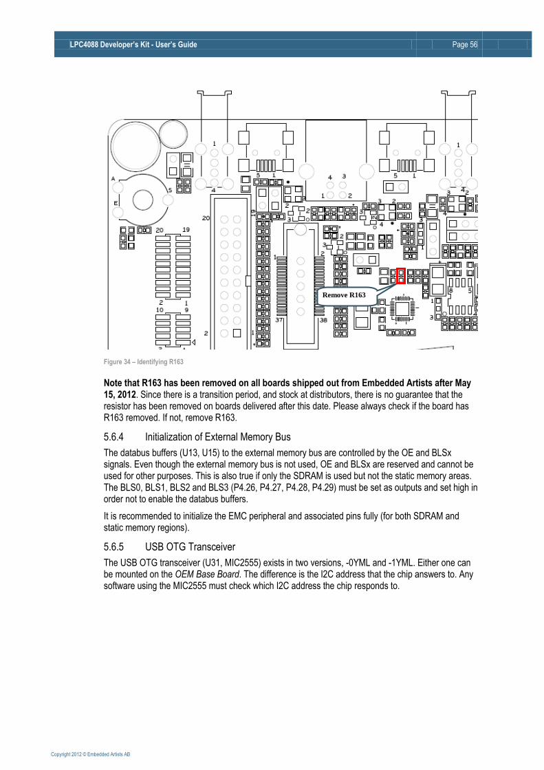
LPC4088 Developer’s Kit - User’s Guide Page 56
Copyright 2012 © Embedded Artists AB
Figure 34 – Identifying R163
Note that R163 has been removed on all boards shipped out from Embedded Artists after May 15, 2012. Since there is a transition period, and stock at distributors, there is no guarantee that the resistor has been removed on boards delivered after this date. Please always check if the board has R163 removed. If not, remove R163.
5.6.4 Initialization of External Memory Bus
The databus buffers (U13, U15) to the external memory bus are controlled by the OE and BLSx signals. Even though the external memory bus is not used, OE and BLSx are reserved and cannot be used for other purposes. This is also true if only the SDRAM is used but not the static memory areas. The BLS0, BLS1, BLS2 and BLS3 (P4.26, P4.27, P4.28, P4.29) must be set as outputs and set high in order not to enable the databus buffers.
It is recommended to initialize the EMC peripheral and associated pins fully (for both SDRAM and static memory regions).
5.6.5 USB OTG Transceiver
The USB OTG transceiver (U31, MIC2555) exists in two versions, -0YML and -1YML. Either one can be mounted on the OEM Base Board. The difference is the I2C address that the chip answers to. Any software using the MIC2555 must check which I2C address the chip responds to.
Remove R163
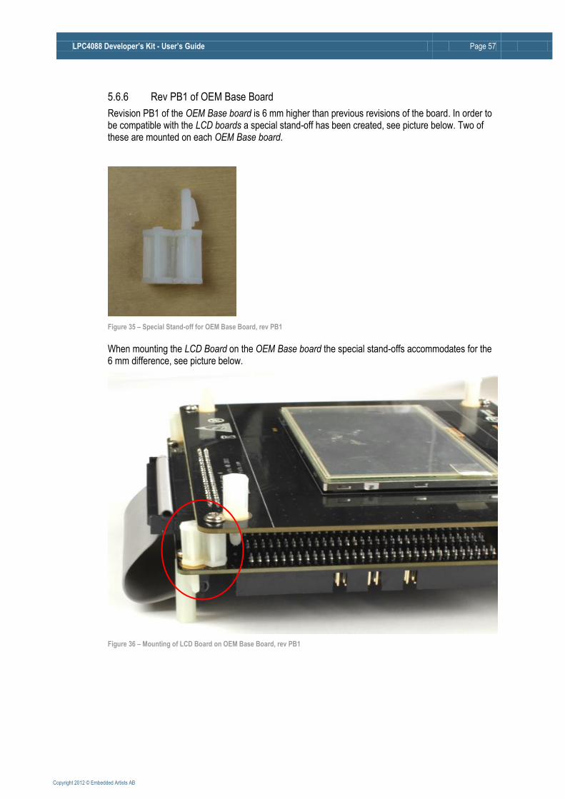
LPC4088 Developer’s Kit - User’s Guide Page 57
Copyright 2012 © Embedded Artists AB
5.6.6 Rev PB1 of OEM Base Board
Revision PB1 of the OEM Base board is 6 mm higher than previous revisions of the board. In order to be compatible with the LCD boards a special stand-off has been created, see picture below. Two of these are mounted on each OEM Base board.
Figure 35 – Special Stand-off for OEM Base Board, rev PB1
When mounting the LCD Board on the OEM Base board the special stand-offs accommodates for the 6 mm difference, see picture below.
Figure 36 – Mounting of LCD Board on OEM Base Board, rev PB1
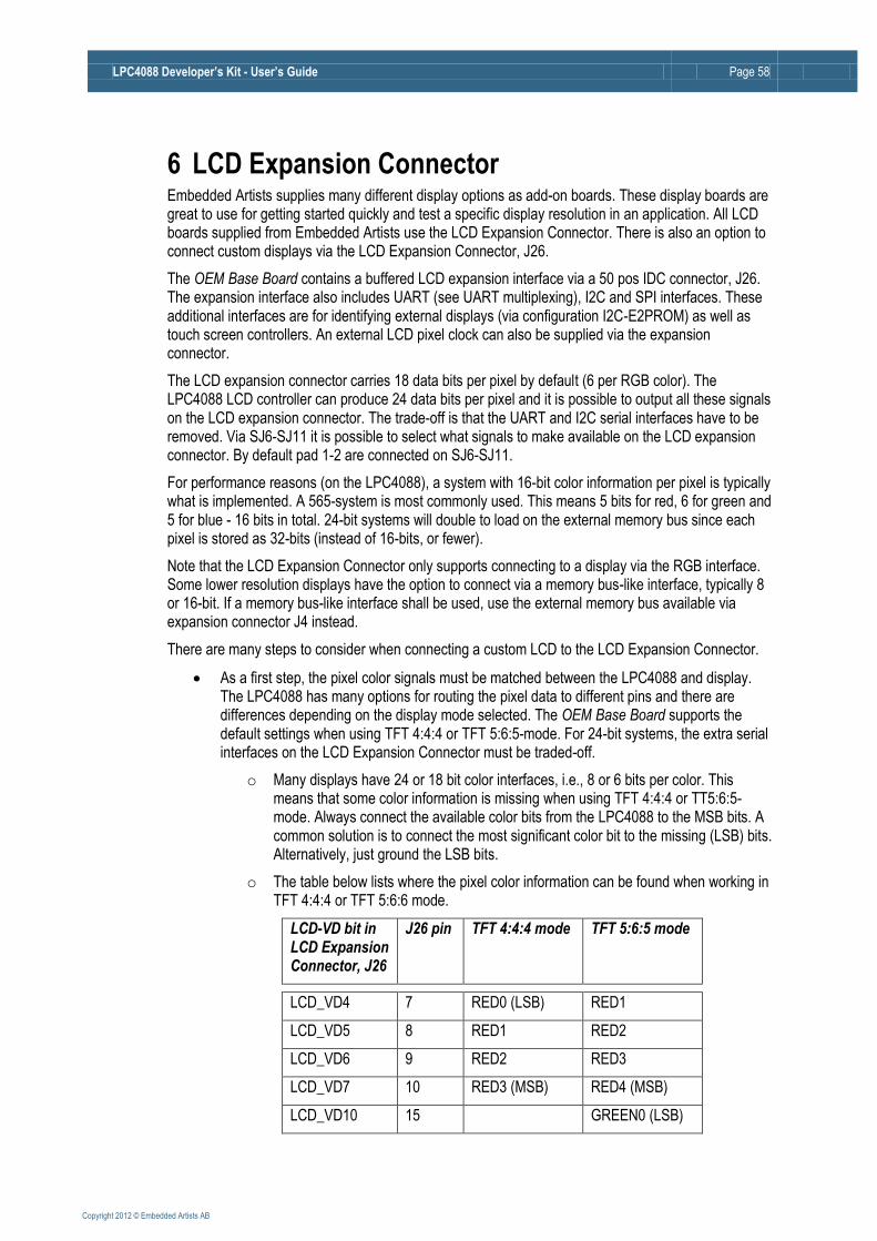
LPC4088 Developer’s Kit - User’s Guide Page 58
Copyright 2012 © Embedded Artists AB
6 LCD Expansion Connector Embedded Artists supplies many different display options as add-on boards. These display boards are great to use for getting started quickly and test a specific display resolution in an application. All LCD boards supplied from Embedded Artists use the LCD Expansion Connector. There is also an option to connect custom displays via the LCD Expansion Connector, J26.
The OEM Base Board contains a buffered LCD expansion interface via a 50 pos IDC connector, J26. The expansion interface also includes UART (see UART multiplexing), I2C and SPI interfaces. These additional interfaces are for identifying external displays (via configuration I2C-E2PROM) as well as touch screen controllers. An external LCD pixel clock can also be supplied via the expansion connector.
The LCD expansion connector carries 18 data bits per pixel by default (6 per RGB color). The LPC4088 LCD controller can produce 24 data bits per pixel and it is possible to output all these signals on the LCD expansion connector. The trade-off is that the UART and I2C serial interfaces have to be removed. Via SJ6-SJ11 it is possible to select what signals to make available on the LCD expansion connector. By default pad 1-2 are connected on SJ6-SJ11.
For performance reasons (on the LPC4088), a system with 16-bit color information per pixel is typically what is implemented. A 565-system is most commonly used. This means 5 bits for red, 6 for green and 5 for blue - 16 bits in total. 24-bit systems will double to load on the external memory bus since each pixel is stored as 32-bits (instead of 16-bits, or fewer).
Note that the LCD Expansion Connector only supports connecting to a display via the RGB interface. Some lower resolution displays have the option to connect via a memory bus-like interface, typically 8 or 16-bit. If a memory bus-like interface shall be used, use the external memory bus available via expansion connector J4 instead.
There are many steps to consider when connecting a custom LCD to the LCD Expansion Connector.
As a first step, the pixel color signals must be matched between the LPC4088 and display. The LPC4088 has many options for routing the pixel data to different pins and there are differences depending on the display mode selected. The OEM Base Board supports the default settings when using TFT 4:4:4 or TFT 5:6:5-mode. For 24-bit systems, the extra serial interfaces on the LCD Expansion Connector must be traded-off.
o Many displays have 24 or 18 bit color interfaces, i.e., 8 or 6 bits per color. This means that some color information is missing when using TFT 4:4:4 or TT5:6:5-mode. Always connect the available color bits from the LPC4088 to the MSB bits. A common solution is to connect the most significant color bit to the missing (LSB) bits. Alternatively, just ground the LSB bits.
o The table below lists where the pixel color information can be found when working in TFT 4:4:4 or TFT 5:6:6 mode.
LCD-VD bit in LCD Expansion Connector, J26
J26 pin TFT 4:4:4 mode TFT 5:6:5 mode
LCD_VD4 7 RED0 (LSB) RED1
LCD_VD5 8 RED1 RED2
LCD_VD6 9 RED2 RED3
LCD_VD7 10 RED3 (MSB) RED4 (MSB)
LCD_VD10 15 GREEN0 (LSB)
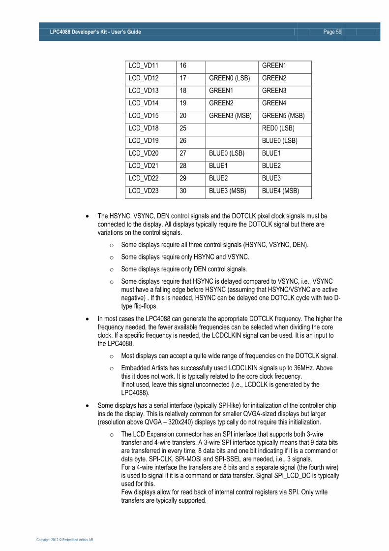
LPC4088 Developer’s Kit - User’s Guide Page 59
Copyright 2012 © Embedded Artists AB
LCD_VD11 16 GREEN1
LCD_VD12 17 GREEN0 (LSB) GREEN2
LCD_VD13 18 GREEN1 GREEN3
LCD_VD14 19 GREEN2 GREEN4
LCD_VD15 20 GREEN3 (MSB) GREEN5 (MSB)
LCD_VD18 25 RED0 (LSB)
LCD_VD19 26 BLUE0 (LSB)
LCD_VD20 27 BLUE0 (LSB) BLUE1
LCD_VD21 28 BLUE1 BLUE2
LCD_VD22 29 BLUE2 BLUE3
LCD_VD23 30 BLUE3 (MSB) BLUE4 (MSB)
The HSYNC, VSYNC, DEN control signals and the DOTCLK pixel clock signals must be connected to the display. All displays typically require the DOTCLK signal but there are variations on the control signals.
o Some displays require all three control signals (HSYNC, VSYNC, DEN).
o Some displays require only HSYNC and VSYNC.
o Some displays require only DEN control signals.
o Some displays require that HSYNC is delayed compared to VSYNC, i.e., VSYNC must have a falling edge before HSYNC (assuming that HSYNC/VSYNC are active negative) . If this is needed, HSYNC can be delayed one DOTCLK cycle with two D-type flip-flops.
In most cases the LPC4088 can generate the appropriate DOTCLK frequency. The higher the frequency needed, the fewer available frequencies can be selected when dividing the core clock. If a specific frequency is needed, the LCDCLKIN signal can be used. It is an input to the LPC4088.
o Most displays can accept a quite wide range of frequencies on the DOTCLK signal.
o Embedded Artists has successfully used LCDCLKIN signals up to 36MHz. Above this it does not work. It is typically related to the core clock frequency. If not used, leave this signal unconnected (i.e., LCDCLK is generated by the LPC4088).
Some displays has a serial interface (typically SPI-like) for initialization of the controller chip inside the display. This is relatively common for smaller QVGA-sized displays but larger (resolution above QVGA – 320x240) displays typically do not require this initialization.
o The LCD Expansion connector has an SPI interface that supports both 3-wire transfer and 4-wire transfers. A 3-wire SPI interface typically means that 9 data bits are transferred in every time, 8 data bits and one bit indicating if it is a command or data byte. SPI-CLK, SPI-MOSI and SPI-SSEL are needed, i.e., 3 signals. For a 4-wire interface the transfers are 8 bits and a separate signal (the fourth wire) is used to signal if it is a command or data transfer. Signal SPI_LCD_DC is typically used for this. Few displays allow for read back of internal control registers via SPI. Only write transfers are typically supported.
LPC4088 Developer’s Kit - User’s Guide Page 60
Copyright 2012 © Embedded Artists AB
Many displays have strict requirements of power sequencing during power up and down. Embedded Artists display boards has an I2C-GPIO expansion chip (PCA9532) and voltage control of +3.3V and +5V to allow power sequencing.
o Embedded Artists recommend that the power sequences outlined in the display datasheets are followed for best long term performance of the display.
For simplicity, Embedded Artists has added a configuration i2c-e2prom in the display add-on boards that contains information about the connected display. This simplified development of portable software.
o A standard 24LC64 chip is used with i2c-address 0x56 (1.0.1.0.1.1.0.rw). A0 on the chip is connected to GND and A1/A2 to VCC to get address 0x56.
Some displays also require a reset signal after VCC/VDD has stabilized. In that case the I2C-GPIO expansion chip can be used to create this signal. Alternatively a free GPIO signal in the LCD Expansion Connector can be used.
All TFT LCDs must have a control for backlight. A constant current source is needed. Some displays have one LED string while others have 2-4 strings making control slightly more complicated.
o OLEDs do not require separate backlight since the pixels transmit light themselves.
As a final step a touch screen interface is typically needed.
o Embedded Artists display boards often use the TSC2046 from TI. It has a simple SPI interface.
o Capacitive touch screen controllers typically have I2C or SPI interfaces.
Do not forget that some displays have configurations pins for selecting interface type functionality.
LPC4088 Developer’s Kit - User’s Guide Page 61
Copyright 2012 © Embedded Artists AB
7 Troubleshooting This chapter contains information about how to troubleshoot boards that does not seem to operate properly. It is strongly advised to read through the list of tests and actions that can be done before contacting Embedded Artists. The different tests can help determine if there is a problem with the board, or not. For return policy, please read Embedded Artists’ General Terms and Conditions
document (can be found at http://www.embeddedartists.com/shop/).
7.1 Powering
The first step is to make sure that powering works properly. The input power interface is described in section 4.23 .
1. Disconnect the powering and removed the OEM Board, i.e., remove it from the socket (J1). All other connections to the OEM Base Board shall also be removed.
2. Connect a stable DC supply (+5V, positive center) to J24. Minimum current capability shall be 1A for this test. The noise level should be minimal, less than 50mV.
3. Measure the +5V and +3.3V voltages with the help of the voltage measuring pads on the OEM Base Board. Acceptable range for the +5V voltage is 4.5V to 5.5V. Acceptable range for the +3.3V voltage is +3.2V to +3.4V. If the reset-LED is dimming instead of being clearly on or off, it is also a sign that the supply voltages are not stable and outside of valid ranges. If problem; since the OEM board is disconnected and there is normally no big current consumption on passive OEM Base Board, it is likely that some part of the OEM Base Board consumes a lot of current. It might be possible to locate the faulty section/component by checking component temperatures with the finger tip. Be careful because faulty components can get very hot.
4. Verify that there are no voltage dips on the supply. A typical indication of this is that the reset-LED flash from time to time. An oscilloscope can detect voltage dips; measure the supply voltage in AC mode. Set horizontal resolution to 50mV per square. Set the trigger to normal mode and adjust the trigger to 50mV below the normal level. That way, the oscilloscope will trigger every time a voltage dips occurs. By watching the dips it is possible to judge if there is a problem, or not.
5. Verify that the reset-LED flash when pressing the reset push-button. The LED should also light shortly after releasing the push button. The extra “LED on time” is very short but still noticeable (typically a 1/5 of a second, i.e., 200mS).
6. Disconnect the powering and mount the OEM Board again (in J1). Now, measure the +5V and +3.3V voltages again (see step 2 above). If the +5V voltage is below acceptable range it is a sign of too weak power supply to the board. If the reset-LED starts dimming instead of being clearly on or off, it is also a sign of too weak power supply to the board. If the reset-LED always light now when the OEM Board is mounted it is a sign of too weak power supply or a serious error on the OEM Board. When doing this test, be sure to not have any SWD/JTAG interface connected or any external source driving the reset signal. Verify that the reset-LED flash when pressing the reset push-button.
7. In section 4.3 it is described how to measure the current consumption of the OEM Board. Measure the voltage over J2 while pressing the reset push-button constantly. This will give the passive current consumption of the OEM Board, i.e., when the board is in reset. Valid range is 100-350mV (which corresponds to 20-70 mA). If current consumption is outside of this range, it is an indication that something can be wrong with the OEM board. Note that the valid range is quite wide. Being outside this does not necessarily mean that something is
LPC4088 Developer’s Kit - User’s Guide Page 62
Copyright 2012 © Embedded Artists AB
wrong. More symptoms than this is needed to judge if a board is wrong, or not. Do not forget to press the reset push-button all the time during this measurement. Redo the test in case of uncertainty.
8. Now, measure the current consumption of the OEM Board when it is running an application. It is a problem to not have a specified application running because the current consumption can vary widely between different applications. The current consumption shall increase compared to the previous test (in case an application is running). It is recommended to download one of the precompiled sample applications from the LPC4088 Developer’s Kit support page on the Embedded Artists web site. How to download is explained in next section. The sample application s_sdram.hex has for example a known current consumption range. The valid range is 650-900m V (which corresponds to 130-180mA). The current consumption varies between different sample applications depending on which peripherals that are active. A running application will in general give a range of 400-700mV (which corresponds to 80-140mA)
9. In most cases it is possible to power the board via the USB interface, J25 (the UART-to-USB bridge mini-B USB connector). Redo tests 3) to 8) above again with USB powering. Connect J25 directly to a PC with the USB cable included in the Developer’s Kit. Note that not all PC:s and/or laptops can power the board. In such cases, a USB hub with independent powering can work. In this case, connect J25 to a USB Hub, which in turn is connected to a PC.
7.2 Contact with OEM Board MCU
The second step is to make sure that the LPC4088 MCU on the OEM Board is working.
Test that it is possible to download one of the precompiled test programs that exist on Embedded Artists support site. Use Flash Magic to download code over the UART-to-USB bridge. See section 5.4.1 for details how to download. Make sure both jumpers in JP20 are inserted and that correct settings in Flash Magic are used.
Optionally test that it is possible to download via the JTAG/SWD interface. A JTAG/SWD debug interface us then needed. The low-cost LPCXpresso target board series from NXP contains a JTAG/SWD debug interface called LPC-LINK that can be used for this. Other brands will also work.
7.3 Using Test Program to Verify Correct Operation
The third step is to utilize the just downloaded precompiled sample applications, one after one, to verify correct operation of individual parts of the OEM Board as well as the OEM Base Board. While doing these tests, be sure to not have anything connected to the system.
There are sample applications for testing/verifying operation of:
1. Analog input
2. I2S-E2PROM
3. NAND flash
4. Accelerometer
5. I2S audio via codec
6. Ethernet
7. SD/MMC memory card interface
8. Joystick
9. LEDs and push-buttons (via the PCA9532)
10. Audio via analog output

LPC4088 Developer’s Kit - User’s Guide Page 63
Copyright 2012 © Embedded Artists AB
11. I2C temperature sensor
12. UART
13. USB Device (HID example). Make sure the jumper settings are correct when doing this test.
14. USB Host. Make sure the jumper settings are correct when doing this test.
15. External SDRAM
16. SPIFI
LPC4088 Developer’s Kit - User’s Guide Page 64
Copyright 2012 © Embedded Artists AB
8 Further Information The LPC4088 microcontroller is a complex circuit and there exist a number of other documents with a lot more information. The following documents are recommended as a complement to this document.
[1] NXP LPC4088 Datasheet <TBD>
[2] NXP LPC4088 User’s Manual <TBD>
[3] NXP LPC4088 Errata <TBD>
[4] ARM Processor Documentation Documentation from ARM can be found at: http://infocenter.arm.com/.
[5] Information on different ARM Architectures http://www.arm.com/products/processors/technologies/ instruction-set-architectures.php
[6] ARMv7-M Architecture Reference Manual. Document identity: DDI 0403D http://infocenter.arm.com/help/index.jsp?topic=/com.arm.doc.ddi0403c/index.html
[7] Cortex-M4 Technical Reference Manual. Revision: r0p1 http://infocenter.arm.com/help/index.jsp?topic=/com.arm.doc.ddi0439c/index.html
[8] LPCXpresso IDE: NXP's low-cost development platform for LPC families, which is an Eclipse-based IDE. http://ics.nxp.com/lpcxpresso/
[9] LPC2000 Yahoo Group. A discussion forum dedicated entirely to the NXP LPC2xxx series of microcontrollers. http://tech.groups.yahoo.com/group/lpc2000/
Note that there can be newer versions of the documents than the ones linked to here. Always check for the latest information/version.