lpc4088 display module user’s guide - embedded artists · 2018-06-20 · this document is a...
TRANSCRIPT

LPC4088 Display Module - User’s Guide
Copyright 2015 © Embedded Artists AB
EA2-USG-1403 Rev A
LPC4088 Display Module User’s Guide
Get Up-and-Running Quickly and Start Developing Your Application On Day 1!
LPC4088 Display Module - User’s Guide Page 2
Copyright 2015 © Embedded Artists AB
Embedded Artists AB Davidshallsgatan 16 211 45 Malmö Sweden
[email protected] http://www.EmbeddedArtists.com
Copyright 2015 © Embedded Artists AB. All rights reserved.
No part of this publication may be reproduced, transmitted, transcribed, stored in a retrieval system, or translated into any language or computer language, in any form or by any means, electronic, mechanical, magnetic, optical, chemical, manual or otherwise, without the prior written permission of Embedded Artists AB.
Disclaimer
Embedded Artists AB makes no representation or warranties with respect to the contents hereof and specifically disclaim any implied warranties or merchantability or fitness for any particular purpose. Information in this publication is subject to change without notice and does not represent a commitment on the part of Embedded Artists AB.
Feedback
We appreciate any feedback you may have for improvements on this document. Please send your comments to [email protected].
Trademarks
All brand and product names mentioned herein are trademarks, services marks, registered trademarks, or registered service marks of their respective owners and should be treated as such.

LPC4088 Display Module - User’s Guide Page 3
Copyright 2015 © Embedded Artists AB
Table of Contents 1 Document Revision History 5
2 Introduction 6
2.1 Features 6
2.2 ESD Precaution 7
2.3 Warranty Hints and General Handling Care 7
2.4 Code Read Protection 8
2.5 CE Assessment 8
2.6 Other Products from Embedded Artists 8
2.6.1 Design and Production Services 8
2.6.2 OEM / LPCXpresso / QuickStart Boards and Kits 8
3 Getting Started 9
3.1 Usage Models 9
3.2 Hardware Overview 11
3.3 Powering 12
3.4 Demo/Test Application 13
3.5 Software Development 13
3.5.1 mbed Framework 13
3.5.2 LPCOpen Framework 14
3.5.3 Setup Own Framework 14
3.6 Program Download 15
3.7 How to Debug 18
4 Connectors 19
4.1 Main Interface Connector, J11 19
4.2 mbed micro-B USB Connector, J9 22
4.3 Debug Interface, J7 23
4.4 Tag-Connect Debug Interface, J6 23
4.5 RJ45 Ethernet Connector, J1 24
4.6 USB Host/Device Connectors, J5/J4 24
4.7 RF Module Interface Connector, J2 24
4.8 Memory Card Interface Connector, J3 26
4.9 Expansion Connector, J10 26
5 Expansion 27
5.1 General Design Checklist 30
6 How to Embed / Integrate the Display Module 33
6.1 Powering 33
6.1.1 +5V Power supply example 33
6.2 Optional VBAT Powering 34
6.3 Interface to Environment 34

LPC4088 Display Module - User’s Guide Page 4
Copyright 2015 © Embedded Artists AB
6.4 Mechanical Integration 34
6.5 CE Declaration of Conformity 35
6.6 Contact Embedded Artists 35
7 Custom Specific Versions 36
8 Future Proof Design - BIOS 37
9 Things to Note 38
9.1 Current Consumption and Limits of USB Ports 38
9.2 CMSIS-DAP program download time 38
9.3 HDK USB Mass-storage does not work on Mac - LPC4088 locks up 38
9.4 Cannot download binary to LPC4088 via Cortex Debug Connector 38
9.5 Updating the HDK 38
9.5.1 Update Procedure 39
10 Troubleshooting 40
10.1 Powering 40
10.2 Program Download to LPC4088 41
10.3 Using Test Application to Verify Correct Operation 41
11 Appendix: Rev A Board Differences 44
12 Further Information 45

LPC4088 Display Module - User’s Guide Page 5
Copyright 2015 © Embedded Artists AB
1 Document Revision History
Revision Date Description
PA1 2014-12-10 First version.
PA2 2015-01-26 Update all sections for rev B boards. Appendix added to cover rev A boards.
PA3 2015-01-29 Moved mbed Getting Started Tour to SW manual.

LPC4088 Display Module - User’s Guide Page 6
Copyright 2015 © Embedded Artists AB
2 Introduction Thank you for buying Embedded Artists’ LPC4088 Display Module, which is based on NXP’s ARM Cortex-M4F LPC4088 microcontroller.
This document is a User’s Guide that describes the LPC4088 Display Module mainly from a hardware point of view. Some basic software related issues are also addressed but there is also a separate software manual for the software framework that has been created.
2.1 Features
Embedded Artists’ LPC4088 Display Module lets you get up-and-running quickly with graphical applications, the mbed-platform and Cortex-M4F programming in general. Communication interfaces, large on-board memories and LCD controller/display enables graphical user interface (GUI) and communication gateway designs. On-board connectors and industrial design makes the module perfect for product integration.
The features of the display module are:
Several display options (like 4.3" color TFT LCD, 480x272 pixels, and 5" color TFT LCD, 800x480 pixels)
Resistive or capacitive touch panel with integrated controller to off-load the MCU
LCD backlight voltage generator, controlled via PWM signal
16- and 24-bit color depth supported
120 MHz Cortex-M4F LPC4088 MCU from NXP
MCU core has floating point and DSP support in hardware
On-module memories
512 kB LPC4088 on-chip flash
96 kB LPC4088 on-chip SRAM
32 MB SDRAM (32-bit databus width for high bandwidth access)
16 MB QSPI flash on SPIFI interface (for both program code and data)
4032 Byte LPC4088 on-chip E2PROM (for parameter storage)
1 Kbit E2PROM with EUI-48™ number (for Ethernet MAC address)
8 Kbyte E2PROM with BIOS code - future proof design! (see chapter 8 )
Extensive Interfaces and Peripherals
100/10 Mbps Ethernet with RJ45 connector
USB Host interface with USB-A connector
USB Device interface with mini-B connector
20 pos XBeeTM compatible connector for RF module add-on
Very simple expansion for custom specific I/O via 46 pos, 100 mil pitch pin header (second USB interface, UART, SPI, I2C, ADC, DAC, CAN, GPIO, timer, etc)
LPC4088 On-chip RTC, with super capacitor backup
uSD/transflash memory card interface for optional memory capacity
Reset generation, 4 LEDs, pushbutton on P2.10
LPC4088 Display Module - User’s Guide Page 7
Copyright 2015 © Embedded Artists AB
Debug interfaces
mbed-enabled via on-board HDK (CMSIS-DAP interface, USB drag-n-drop, Virtual COM port)
10 position SWD/JTAG connector (ARM standard Cortex Debug Connector)
6 position SWD Tag-ConnectTM connector
Powering
On-module +3.3V linear power supply
External +5V supply needed, either via USB or external +5V DC
Optional, external VBAT supply for RTC
Dimensions
Compact size: 123 x 100 mm
Other
Proper ESD protection on communication interfaces
Multilayer PCB design for best EMC performance, with controlled impedance and length matched routing for critical signals
EMC, EMI and ESD tested
Supported by the mbed SDK and online tools
Supported by professional tools and middleware
Wide/extended temperature range (-20 to +60/70 degrees Celsius, limited by LCD)
ISO 9001:2008 / ISO 14001:2004 produced
Production and shipping compensated for carbon dioxide emission
2.2 ESD Precaution
Please note that the LPC4088 Display Module come without any case/box and all components are exposed for finger touches – and therefore extra attention must be paid to ESD (electrostatic discharge) precaution. Only qualified personnel shall handle the product.
Make it a habit always to first touch the metal surface of one of the USB or Ethernet connectors for a few seconds with both hands before touching any other parts of the boards. That way, you will have the same potential as the board and therefore minimize the risk for ESD.
In general touch as little as possible on the boards in order to minimize the risk of ESD damage.
Note that Embedded Artists does not replace boards that have been damaged by ESD.
2.3 Warranty Hints and General Handling Care
Handle the LPC4088 Display Module with care. The board is not mounted in a protective case/box and is not designed for rough physical handling. Only qualified personnel shall handle the product. Connectors can wear out after excessive use.
Do not exercise excessive pressure on the LCD glass area. That will damage the display. Also, do not apply pressure on the flex cables connecting the LCD/touch screen. These are relatively sensitive and can be damaged if too much pressure is applied to them.

LPC4088 Display Module - User’s Guide Page 8
Copyright 2015 © Embedded Artists AB
Embedded Artists products are subject to manufacturer’s guarantee as long as the products are handled with adequate care and caution and in accordance to this manual.
For exact details about warranty, please read the General Terms and Conditions document that can be found at http://www.embeddedartists.com/shop/
The warranty does not cover defects caused by improper or inadequate installation, maintenance or handling by the user, unauthorized modification or misuse, operation outside the specification a non-compliance of this manual and related documents. In case of doubt, please contact Embedded Artists prior to intended activity.
Note that Embedded Artists does not replace boards where the LCD has been improperly handled. Also note that the warranty does also not cover any defects or damages of other equipment connected to the Embedded Artists product, faulty or not.
2.4 Code Read Protection
The LPC4088 microcontroller has a Code Read Protection function (specifically CRP3, see datasheet for details) that, if enabled, will make the LPC4088 impossible to reprogram (unless the user program has implemented such functionality in firmware).
Note that Embedded Artists does not replace LPC4088 Display Modules where the LPC4088 has CRP3 enabled. It’s the user’s responsibility to not invoke this mode by accident.
2.5 CE Assessment
The LPC4088 Display Module is CE marked. See separate CE Declaration of Conformity document.
The LPC4088 Display Module is a class A product. In a domestic environment this product may cause radio interference in which case the user may be required to take adequate measures.
EMC emission test has been performed on the LPC4088 Experiment Bundle. Standard interfaces like Ethernet, USB, serial have been in use. General expansion connectors where internal signals are made available (for example processor pins) have been left unconnected. Connecting other devices to the product via the general expansion connectors may alter EMC emission. It is the user’s responsibility to make sure EMC emission limits are not exceeded when connecting other devices to the general expansion connectors of the LPC4088 Display Module.
2.6 Other Products from Embedded Artists
Embedded Artists have a broad range of microcontroller based boards that are very low cost and developed for prototyping / development as well as for OEM applications (i.e., for integration). Modifications for OEM applications can be done easily, even for modest production volumes. Contact Embedded Artists for further information about design and production services.
2.6.1 Design and Production Services
Embedded Artists provide design services for custom designs, either completely new or modification to existing boards. Specific peripherals and I/O can be added easily to different designs, for example, communication interfaces, specific analog or digital I/O, and power supplies. Embedded Artists has a broad, and long, experience in designing industrial electronics in general and with NXP’s LPC microcontroller families in specific. Our competence also includes wireless and wired communication for embedded systems.
Contact us at [email protected] for a discussion about how we can help you!
2.6.2 OEM / LPCXpresso / QuickStart Boards and Kits
Visit Embedded Artists’ web page, www.EmbeddedArtists.com, for information about other products.
LPC4088 Display Module - User’s Guide Page 9
Copyright 2015 © Embedded Artists AB
3 Getting Started This chapter contains information about how to get acquainted with the LPC4088 Display Module. Please read this section first before you start using the board - it will be well spent time!
Embedded Artists' has a family of Display Modules that are self-contained, intelligent modules with many usage scenarios. There are different display options in the family and new are easily created based on customer requirements.
There are many reasons to use a display module - all of them will make your life easier and less stressful and saves your company a lot of money!
Save development time and cost - focus on the application Being able to start with a proven design gets you started immediately.
o Extensive SW frameworks to start from! You can focus on your application instead of all infrastructure software.
o Easy to expand HW If needed, it is simple to add an expansion board that contains specific hardware that might be needed. You no longer have to maintain a big platform. You can focus on maintaining the expansion board that contains your core interfaces.
Long term availability and Future safe design Embedded Artists offers long term availability of display modules along with a future safe design principle that allow changing displays on the modules without changing the application software.
Multiple displays options Your customers may have different requirements on your product and want different display options. Or maybe you want to have different product options, involving different display options. Either way, the same HW/SW platform can drive many different displays (different sizes and resolution, different brightness and different touch panel solutions).
Pre-CE tested The display modules are designed for integration and have been EMC, EMI and ESD tested. This increase the likelihood for your final product to also pass tests.
On-board debugger There is an on-board debug interface that simplifies program download and debugging.
3.1 Usage Models
A common usage scenario is to add a display module to an embedded system that already exist. This embedded system typically has an old user interface that needs to be updated to a more modern look-and-feel. The display module acts as a standalone front panel that handles the new graphical Human Machine Interface (HMI). There are several benefits with this solution:
No need for a complete redesign of the hardware and software of the existing embedded system.
Different display sizes can be offered to customers.
Retrofitting existing systems is possible (sold as an upgrade).
The existing embedded system can exchange high-level commands with the display module when controlling the graphical elements.

LPC4088 Display Module - User’s Guide Page 10
Copyright 2015 © Embedded Artists AB
The picture below illustrates this usage scenario.
Figure 1 – LPC4088 Display Module HMI/GUI Usage Scenario
A second usage scenario is to build the complete embedded system around the display module. The LPC4088 Display Module is built around the LPC4088 MCU from NXP. It has a very capable Cortex-M4F core, running at up to 120MHz. There is lots of memory, communication interfaces and expansion possibilities on the module. There are several benefits with this solution:
The core design has already been done. The only thing needed is a the expansion board design for custom specific interfaces and functions that the core design cannot implement.
o Low total ownership cost - only need to maintain the expansion board
Comprehensive software framework exist - the designer can start the real software development immediately.
Different display sizes can be offered to customers.
The picture below illustrates this usage scenario. If the display module is a standalone solution, an expansion board is likely part of the design, but not always. In many cases, the existing interfaces on the display module are just what is needed. Chapter 5 covers how to design an expansion board
Figure 2 – LPC4088 Display Module Standalone Usage Scenario with Expansion Board
LPC4088 Display Module
Existing embedded system in
need of an HMI/GUI LCD with resistive or capacitive touch
panel Local MCU
All interfaces with environment
Communication channel UART, I2C, CAN, Ethernet, USB, RF, GPIO
LPC4088 Display Module
Expansion board LCD with resistive or capacitive touch
panel
Optional local MCU
Expansion Connector, J10 UART, I2C, SPI, I2S, CAN, USB, ADC, DAC, GPIO
Interfaces with environment (split between both boards)

LPC4088 Display Module - User’s Guide Page 11
Copyright 2015 © Embedded Artists AB
3.2 Hardware Overview
The block diagram below presents the major components of the LPC4088 Display Module.
Figure 3 – LPC4088 Display Module Block Diagram
LPC4088 with external memories In the heart of the design there is the LPC4088 MCU from NXP with associated memory; 32MByte of SDRAM with 32-bit databus access, 16MByte of QSPI serial flash and an Ethernet MAC address (EUI-48). The amount of memory is more than enough for most applications. The LPC4088 runs at up to 120MHz and has a Cortex-M4F core.
Display interface The display interface is the glue between the LPC4088 on-chip LCD controller and the actual LCD. Both 16- and 24-bit color depth is supported (controlled via a single GPIO pin). 16-bit color depth supports the 5:6:5 RGB-format. There is a resistive touch panel controller, AR1021, that can handle the low-level sampling and filtering of the touch panel samples, hence off-loading the LPC4088 from this task. The is a DC/DC switched voltage converter that generates a constant current for the display backlight. The current level can be controlled via a PWM signal to allow software to implement backlight dimming.
LCD Different LCDs are supported. Both resistive and capacitive touch panels are supported. LCDs with capacitive touch panel has on-display touch panel controller.
HDK debug interface The mbed Hardware Development Kit (HDK) is included (which is part of what makes the display module an mbed-enabled module). The HDK offers the following features over a common USB connection (the HDK USB port):
1. USB drag-n-drop programming of the LPC4088. A USB Mass Storage Device (MSD) is created and the binary image that the compiler creates can just be dragged and dropped on this drive on the PC-side. The image will then automatically be flashed to the LPC4088 on the board.
LPC4088 with external memories 32MByte SDRAM (x32 databus width), and
16MByte QSPI (serial flash), EUI-48, BIOS code
Display interface 16/24-bit color depth mux, Backlight generation/control,
Resistive touch panel controller
Communication interfaces Ethernet, USB, XBee,
memory card interfaces
LCD with resistive or capacitive touch panel
(on-display TP controller if capacitive touch panel)
Expansion
connector
Other +3.3V Powering
VBAT Powering
Reset generation
Buzzer
4 LEDs
User pushbutton HDK debug
interface
(mbed)

LPC4088 Display Module - User’s Guide Page 12
Copyright 2015 © Embedded Artists AB
2. Virtual serial port, which creates a virtual COM port on the PC-side. There is a serial (UART) channel on the LPC4088 Display Module that can be tunneled over to the PC-side for debug, logging, statistics or other reasons.
3. CMSIS-DAP debug interface, which basically creates an SW debug interface to the LPC4088. The CMSIS-DAP interface is supported by major tool vendors.
Communication interfaces There are multiple communication interfaces, corresponding to LPC4088 key peripherals.
o 100/10 Mbps Ethernet interface, including RJ45 connector and ESD protection.
o USB Host and Device interface, with USB-A and USB-mini B connectors and ESD protection. Note that Host and Device cannot be active at the same time. For a second USB channel, use the expansion connector.
o XBee compatible connector of RF module expansion.
o uSD/transflash memory card connector for large memory requirements.
Expansion connector Several interfaces are available on the easy-to-connect expansion connector. It is a 2x23 pos, 100 mil pitch pin header (male) that allow easy and quick prototyping on an expansion board.
Other The display module also contains a 3.3V linear power supply, VBAT supply including a super capacitor, reset generation, buzzer, 4 LEDs and a user push-button.
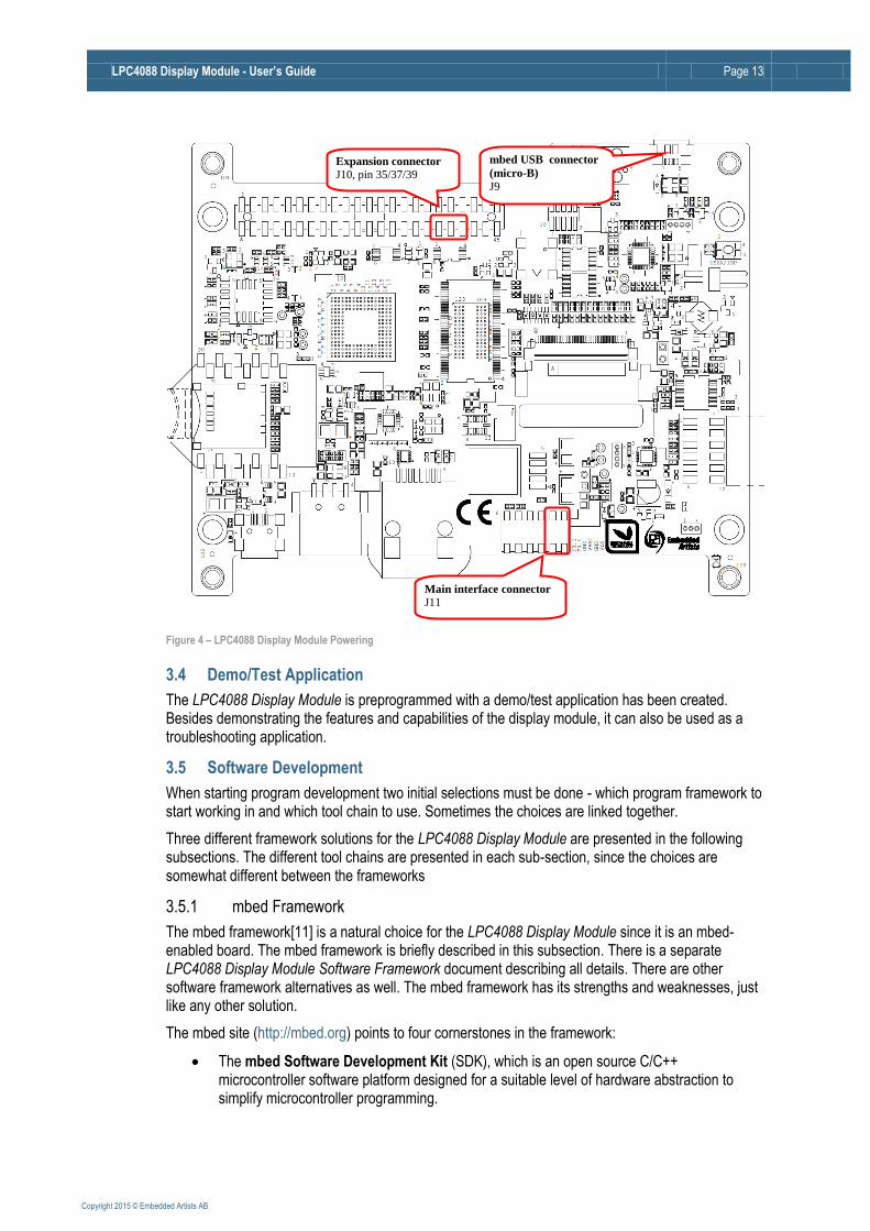
3.3 Powering
Before start handling and working with the display module, read the general handling precautions addressed in chapter 2 , especially about ESD precaution.
There are three ways to power the display module, of which the first two are recommended to start with. An external +5V DC supply is needed. 1-3Amp, depending on what is connected to the display module (for example, USB Devices and RF modules that consume current).
1) mbed HDK micro-B USB connector, J9 This is the natural way to power the display module during program development and initial prototyping. The PC USB interface powers the board. Note that long USB cables can give problems because of too big voltage drops in the cable. Max 1 meter cables with 24 AWG power cords are preferred. Also note that some laptops have lower current limits on their USB host ports. An external, powered USB hub can always be used if there is a problem to directly power the display modules from a USB Host port.
2) Pin 1/2 on main connector J11 This is the natural way to power the display module when it has been deployed/integrated into the end-product.
3) Power supply on expansion board, via expansion connector, J10 The external 5V DC supply can be integrated on an expansion board to create a mode compact and self-contained solution. The display module is then powered (+5V DC) via the expansion connector, J10.
The picture below illustrated where the three powering options can be found on the display module.
LPC4088 Display Module - User’s Guide Page 13
Copyright 2015 © Embedded Artists AB
Figure 4 – LPC4088 Display Module Powering
3.4 Demo/Test Application
The LPC4088 Display Module is preprogrammed with a demo/test application has been created. Besides demonstrating the features and capabilities of the display module, it can also be used as a troubleshooting application.
3.5 Software Development
When starting program development two initial selections must be done - which program framework to start working in and which tool chain to use. Sometimes the choices are linked together.
Three different framework solutions for the LPC4088 Display Module are presented in the following subsections. The different tool chains are presented in each sub-section, since the choices are somewhat different between the frameworks
3.5.1 mbed Framework
The mbed framework[11] is a natural choice for the LPC4088 Display Module since it is an mbed-enabled board. The mbed framework is briefly described in this subsection. There is a separate LPC4088 Display Module Software Framework document describing all details. There are other software framework alternatives as well. The mbed framework has its strengths and weaknesses, just like any other solution.
The mbed site (http://mbed.org) points to four cornerstones in the framework:
The mbed Software Development Kit (SDK), which is an open source C/C++ microcontroller software platform designed for a suitable level of hardware abstraction to simplify microcontroller programming.
Expansion connector J10, pin 35/37/39
mbed USB connector
(micro-B) J9
Main interface connector J11

LPC4088 Display Module - User’s Guide Page 14
Copyright 2015 © Embedded Artists AB
The mbed Compiler is a powerful online IDE that is tightly integrated with the mbed SDK and Developer's Website (mbed.org).
The mbed Hardware Development Kit (HDK), which is an interface design that provides simple USB drag-n-drop programming and CMSIS-DAP debug interface for the LPC4088 microcontroller. The LPC4088 Display Module has an on-board HDK.
The mbed.org community, with extensive documentation in the form of handbooks, cookbooks, project pages, User Forums for getting help and advice from other mbed users, etc.
The mbed Compiler gives you instant access to lightweight C/C++ microcontroller development. It is an online web application IDE (Integrated Development Environment) that you can log in from anywhere and work on Windows, Mac, iOS, Android or Linux. For a quick guide how to write code, compile and download to the LPC4088 Display Module, see chapter Fel! Hittar inte referenskälla..
The mbed Compiler has some limitations, mainly when it comes to debugging. There are alternatives to the online compiler when more professional program development and debugging is needed. The mbed framework and the application code can be exported from the online compiler and imported into an offline tool chain. For more details, see here: http://mbed.org/handbook/Exporting-to-offline-toolchains
Currently there are guides for exporting to:
uVision
LPCXpresso IDE
CodeSourcery
GCC ARM Embedded
IAR Embedded Workbench
Under these tool chains it is possible to perform professional debugging with breakpoints, inspecting variable values, dumping memory regions and even trace the program execution flow (provided the debug probe supports the feature). Remember that the LPC4088 Display Module has an on-board debug interface so an external debug probe is in general not needed. Most tool chains support the CMSIS-DAP standard now.
3.5.2 LPCOpen Framework
LPCOpen[10] has been created by NXP. It is a platform consisting of a large number of libraries and examples that allows you to get started quickly. The platform uses common APIs that work equally across all NXP microcontroller families. It supports the common development tool chains; uVision from Keil/ARM, Embedded Workbench from IAR, and LPCXpresso IDE from NXP.
There is a core driver library containing three important sections:
Chip Driver Layer - Peripheral drivers for the microcontroller
Board Layer - Board specific functions and low level setup code
Examples - Chip family specific examples for peripherals, interfaces, libraries, etc.
LPCOpen also contains some important larger program packages/libraries, like FreeRTOS, LWIP (TCP/IP stack), USB driver and graphical library - all together with bigger project examples.
Embedded Artists has created an LPCOpen port for the LPC4088 Display Module.
3.5.3 Setup Own Framework
There is always the option to roll your own solution and start from scratch to build the needed framework. Most tool chains (LPCXpresso IDE from NXP, uVision from Keil/ARM, Embedded

LPC4088 Display Module - User’s Guide Page 15
Copyright 2015 © Embedded Artists AB
Workbench from IAR, etc.) can create empty program skeletons. Besides an empty main()-function, only the most important startup code for initializing clocks and the very basic functions in the microcontroller is given.
This approach is definitively a possibility and might be a preferred option if for example there is legacy code to be ported to the new platform. The approach will require more reading, and understanding, of the LPC4088 User's Manual from NXP.
3.6 Program Download
This section describes some basic methods for downloading application code to the LPC4088. Note that this section does not describe how to create the application code (write the program and compile it). It is assumed that a binary file exist that represent the application program.
Most program development environments create files that also contains debug information (*.elf file or *.axf file). This way, the integrated debuggers have the information needed when debugging. When these files are stripped from the debug information and just the pure binary file is left, it is often also called hex-file, which is a file format that Intel created a long time ago. It can also be a pure binary file (which is typically called a bin-file).
Note that the on-line mbed compiler create pure binary files without debug information (since this environment does not support debugging in the traditional meaning.
There are four basic methods for program download (the top two methods are the recommended that will give a quick start since it is support by on-board functionality):
- On-board HDK: USB drag-n-drop The on-board HDK (see section 4.2 for more information) creates a USB drag-n-drop programming function. A USB Mass Storage Device (MSD) is created and the binary image that the on-line mbed compiler creates can just be dragged and dropped on this drive on the PC-side. The image will then automatically be flashed to the LPC4088 on the board. Note that any binary file can be dragged and dropped - and programmed. It is not only the on-line mbed compiler that can generate binary files. Normally, however, the generated files also contains debug information. These files must be stripped to generate a binary file that can be used. See the documentation for the used program development environment for details.
- On-board HDK: CMSIS-DAP Interface (SWD/JTAG) The on-board HDK (see section 4.2 for more information) also creates a CMSIS-DAP debug interface, which basically creates a debug interface to the LPC4088. The CMSIS-DAP interface is supported by major program development tool vendors. This interface is not the fastest available (due to limitation of the LPC11U35, the MCU that implements the HDK), but it works very well for hobbyists and semi-professional users. For higher download speed, needed for professional use, an external debug probe is recommended. See next alternative for more details.
- SWD/JTAG via External Debugger The LPC4088 Display Module also offers direct access to the Serial Wire (SW) debug interface of the LPC4088 MCU. Any external debug probe that supports the LPC4088 and the 10-pin SW interface, called the Cortex Debug Connector, can be connected to this interface. The cheap, 15 EUR, LPC-Link 2 debug probe directly supports the 10-pin connector creates a powerful, professional quality debug interface. The first picture below illustrates how LPC-Link2 is directly connected to the Cortex Debug Connector on the LPC4088 Display Module pcb. The second picture illustrates when the Tag-ConnectTM pads are used instead. A special cable (from Tag-Connect) is used.

LPC4088 Display Module - User’s Guide Page 16
Copyright 2015 © Embedded Artists AB
Figure 5 – LPC-Link2 Connected To LPC4088 Display Module
LPC4088 Display Module - User’s Guide Page 17
Copyright 2015 © Embedded Artists AB
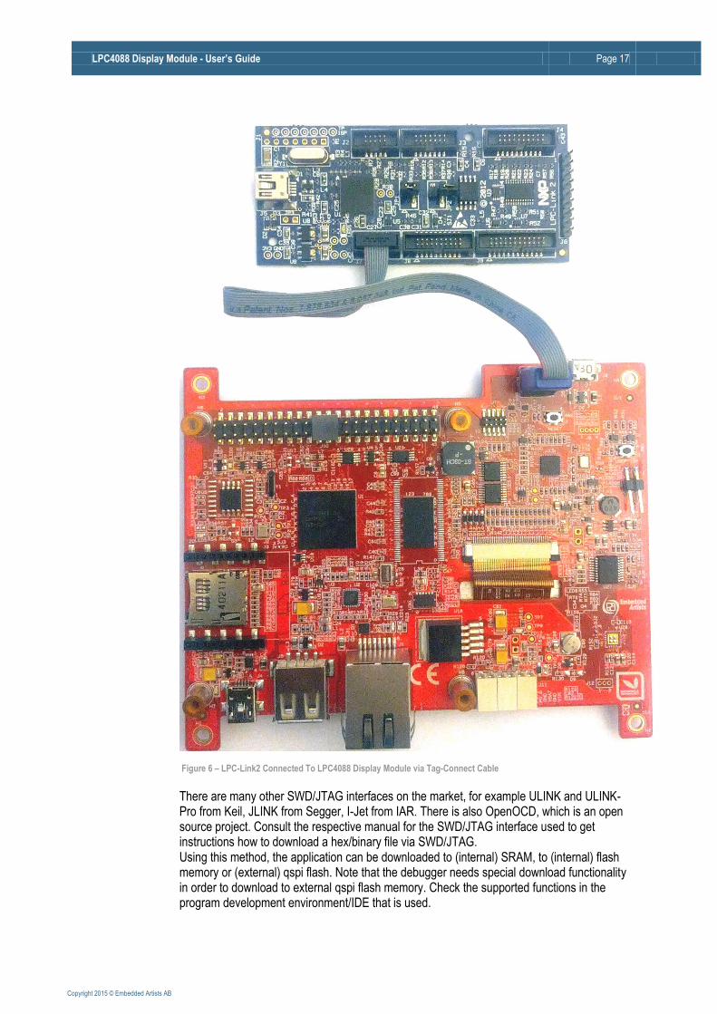
Figure 6 – LPC-Link2 Connected To LPC4088 Display Module via Tag-Connect Cable
There are many other SWD/JTAG interfaces on the market, for example ULINK and ULINK-Pro from Keil, JLINK from Segger, I-Jet from IAR. There is also OpenOCD, which is an open source project. Consult the respective manual for the SWD/JTAG interface used to get instructions how to download a hex/binary file via SWD/JTAG. Using this method, the application can be downloaded to (internal) SRAM, to (internal) flash memory or (external) qspi flash. Note that the debugger needs special download functionality in order to download to external qspi flash memory. Check the supported functions in the program development environment/IDE that is used.

LPC4088 Display Module - User’s Guide Page 18
Copyright 2015 © Embedded Artists AB
- ISP over UART ISP is short for In-System Programming. The LPC4088 contains a bootloader in ROM that is activated by pulling pin P2.10 low during reset. This is easily accomplished by pressing the user pushbutton during reset/power-up. UART0 pins P0.2 (U0_TXD) and P0.3 (U0_RXD) are then used to download the program . An application is needed on the PC for downloading the application code, for example Flash Magic (http://www.flashmagictool.com/). This method is only included to make the list of options complete, but it is not recommended since the other options are simpler and faster alternatives. Also note that the ISP bootloader cannot program the on-board qspi flash. It is possible to use the HDK virtual COM port to communicate with the UART channel on P0.2/P0.3 (called HDK_MBED_TX and HDK_MBED_RX, respectively, in the schematic).
3.7 How to Debug
The debug options are given by the development environment selected. If mbed is selected as framework and the on-line compiler is used, the debug options are very few - basically only printf()-style and flashing LED debugging. This is not acceptable for professional users. If the mbed project is exported to an external development environment, for example the LPCXpresso IDE, then the full debug options are available (like breakpoints, watch-points, etc).
The on-board HDK implements a CMSIS-DAP debug interface that is supported by most development tool vendors. It is not as fast as an external debug probe would be but still acceptable for many applications. For more information, see section 3.6 .

LPC4088 Display Module - User’s Guide Page 19
Copyright 2015 © Embedded Artists AB
4 Connectors This chapter contains information about all connectors on the display module. The picture below locate the connectors that are described in the subsequent sections.
Figure 7 – LPC4088 Display Module Connectors
4.1 Main Interface Connector, J11
This is the main interface connector for the board. It has six positions according to table below. NOTE that position numbering marking on connector J11 is not correct. See Figure 11 above for correct numbering.
Position Usage
1 Vin - external +5V supply.
Consult the display module datasheet for details about valid voltage range, current consumption and allowed voltage ripple/noise.
Depending on configuration and application, current consumption can vary between
Expansion connector J10
Pin 1/2 - 45/46 (left to right)
SWD debug
connector
J7
Tag-Connect
connector
J6
mbed USB
connector
(micro-B) J9
USB Device
connector (mini-B) J4
USB Host
connector (A) J5
RJ45 Ethernet connector
J1
Main interface connector J11 Pos 6-1 (left to right)
NOTE that position numbering
marking on connector is different.
Correct is Pos 6-1 (left to right).
XBee interface
connector J2
transflash/
uSD connector J3

LPC4088 Display Module - User’s Guide Page 20
Copyright 2015 © Embedded Artists AB
1-3 Amp. Expansion board, LCD backlight, RF module, Ethernet and USB Host interfaces can all make significant contribution to the current consumption.
A Schottky series diode on the display module protects against reverse polarity.
2 GND - ground for Vin supply
3 VBAT - optional external supply for LPC4088 real-time clock (RTC).
Consult the display module datasheet for details about valid voltage range and current consumption.
If no external supply exist, leave position open.
Note that an external supply is not (trickle) charged from the board internal.
4 GND - ground for VBAT supply
5 P0.0 - connected via 100 ohm series resistor to pin P0.0 on the LPC4088 MCU. 0-3.3V logic, 5V tolerant. Functionality controlled by firmware running on LPC4088.
Can be UART-TXD (external transceiver needed for RS232 compatibility).
Can be CAN-RD (external CAN transceiver needed).
Can be I2C-SDA (on-board 5K pull-up resistor).
Can be general GPIO.
6 (closest to RJ45 Ethernet connector, J1)
P0.1 - connected via 100 ohm series resistor to pin P0.1 on the LPC4088 MCU. 0-3.3V logic, 5V tolerant. Functionality controlled by firmware running on LPC4088.
Can be UART-RXD (external transceiver needed for RS232 compatibility).
Can be CAN-TD (external CAN transceiver needed).
Can be I2C-SCL (on-board 5K pull-up resistor).
Can be general GPIO.
J11 is a quick and reliable wire-to-board connector from AVX, series 9276 (http://www.avx.com/docs/Catalogs/9276.pdf). Solid or stranded wires between 18-24 AWG are inserted directly into the connector. The table below lists the 18-24 AWG equivalents in inch, mm and mm2.
AWG Diameter in inch Diameter in mm Area in mm2
18 0.040 inch 1.02 mm 0.823 mm2
20 0.032 inch 0.81 mm 0.512 mm2
22 0.025 inch 0.64 mm 0.326 mm2
24 0.020 inch 0.51 mm 0.205 mm2
The absolute maximum diameter of a wire is 1.2 mm. The maximum diameter for the insulator is 2.1 mm.
The picture below (from the AVX connector's datasheet) illustrates how to insert a wire. The strip length (removed insulation) shall be 4-5mm. Stranded wires shall be twisted together before insertion.

LPC4088 Display Module - User’s Guide Page 21
Copyright 2015 © Embedded Artists AB
Figure 8 – AVX series 9276 Wire Assembly
When removing a wire, a small bladed extraction tool (1.6 mm wide and 0.5 mm thick) is inserted in the slot above the cable to release it. AVX sells this tool with part number: 06-9276-7001-01-000. The picture below illustrates the process of wire extraction.
Note that the AVX connector is design for up to 5 insertions/extractions per wire position.
Figure 9 – AVX series 9276 Wire Extraction

LPC4088 Display Module - User’s Guide Page 22
Copyright 2015 © Embedded Artists AB
4.2 mbed micro-B USB Connector, J9
J9 is a micro-B USB connector to the on-board mbed Hardware Development Kit (HDK). This is part of what makes the display module an mbed-enabled. The HDK offers the following features over a common USB connection (J9):
4. USB drag-n-drop programming of the target processor (LPC4088). A USB Mass Storage Device (MSD) is created and the binary image that the compiler creates can just be dragged and dropped on this drive on the PC-side. The image will then automatically be flashed to the LPC4088 on the board.
5. Virtual serial port, which creates a virtual COM port on the PC-side. There is a serial (UART) channel on the LPC4088 QuickStart Board that can be tunneled over to the PC-side for debug, logging, statistics or other reasons.
6. CMSIS-DAP debug interface, which basically creates an SW debug interface to the LPC4088. The CMSIS-DAP interface is supported by major tool vendors.
The HDK functionality is implemented in a separate microcontroller (LPC11U35). It communicates with the PC over a USB interface and with the LPC4088 via the (Cortex) debug interface. The picture below illustrates the connections and also the physical place of the HDK microcontroller.
Figure 10 – LPC4088 Display Module and HDK
HDK
Separate MCU
LPC4088, memories and interfaces
debug interface
USB interface

LPC4088 Display Module - User’s Guide Page 23
Copyright 2015 © Embedded Artists AB
The micro-B USB connector signals are ESD protected.
Note that the mbed USB connector can be used for powering during development but it is not suitable for being the permanent powering method for integrated display modules.
4.3 Debug Interface, J7
J7 is a 2x5 position, 50 mil pitch, standard Cortex Debug Connector as defined by ARM. Debugging with the LPC4088 defaults to JTAG. Once in the JTAG debug mode, the debug tool can switch to Serial Wire Debug mode. For details about the debug and trace capabilities of the LPC4088, see the chip user manual from NXP.
Note that the on-board debug interface (mbed HDK) must not be powered when using the debug interface (J7) for accessing the LPC4088 MCU. This is accomplished by removing resistor R98.
The table below lists the pin functions on the 2x5 pos connector.
Pin SWD mode JTAG mode Notes
1 VCC VCC 3.3V logic
2 SWDIO TMS 33K ohm pull-up resistor and ESD protected.
3 GND GND
4 SWCLK TCK 33K ohm pull-down resistor and ESD protected.
5 GND GND
6 SWO TDO 33K ohm pull-up resistor and ESD protected.
7 Key - NC (RTCK) This position is sometimes a key-position, meaning that the pin shall not exist on the connector.
8 NC TDI 33K ohm pull-up resistor and ESD protected.
9 GND detect GND detect Can be used by debug probe to detect that an MCU is connected.
10 NRST NRST 15K ohm pull-up resistor and ESD protected.
Any debugger supporting the LPC4088 MCU and is compatible with the ARM's Cortex Debug connector standard will work. One example is the low-cost LPC-Link2 debug interface.
4.4 Tag-Connect Debug Interface, J6
J6 is a 6 position Tag-Connect pad according to the TC2030-CTX Plug-of-NailTM format. For details see here: http://www.tag-connect.com/TC2030-CTX
The cable connects to the display module pcb (J6 pads) in one end and the other end has a 2x5 pos, 50 pitch, female IDC-style connector. Many debuggers has this interface connector, for example the low-cost LPC-Link2 debug interface and ULINK2 from Keil/ARM.
Note that the on-board debug interface (mbed HDK) must not be powered when using the Tag-Connect debug interface (J6) for accessing the LPC4088 MCU. This is accomplished by removing resistor R98.
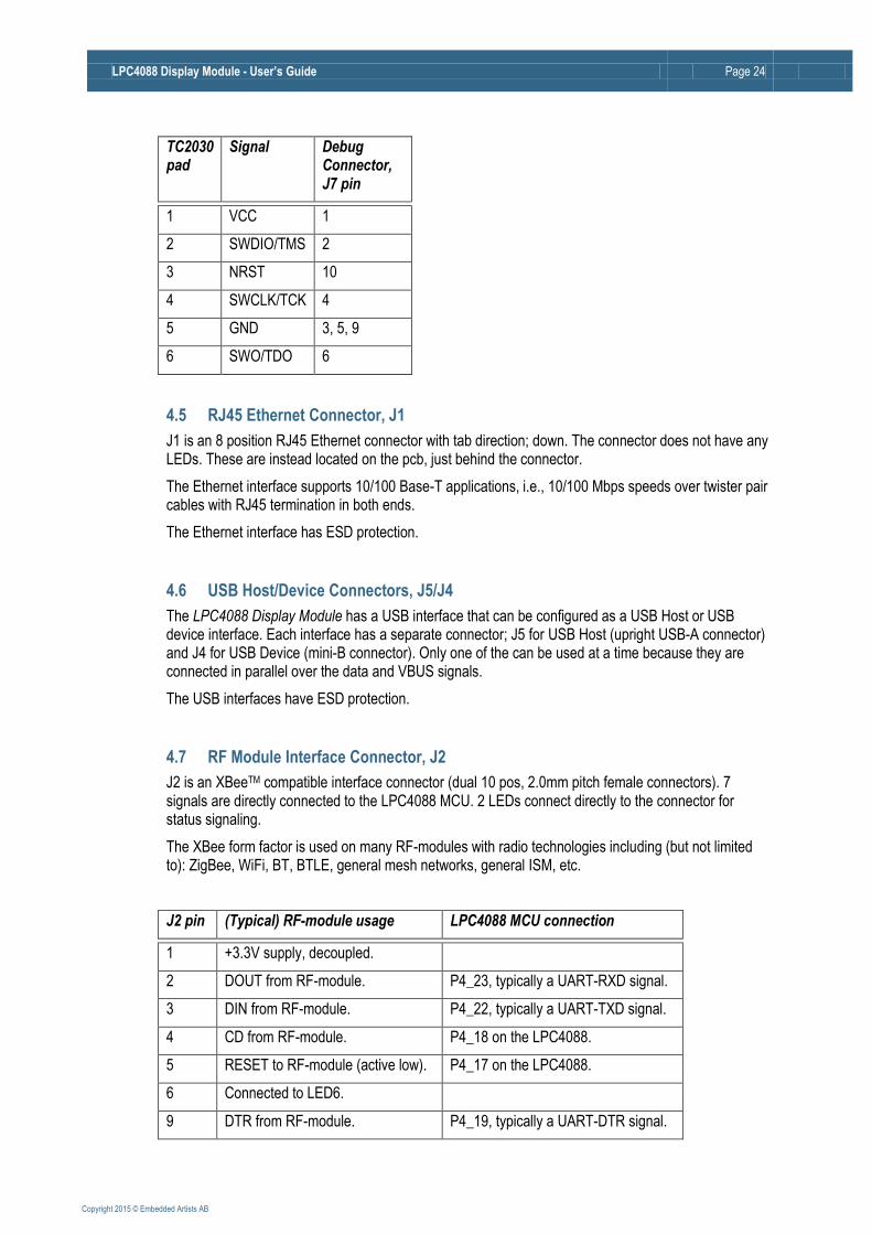
J6 is connected in parallel with the debug interface connector, J7, see table below.
LPC4088 Display Module - User’s Guide Page 24
Copyright 2015 © Embedded Artists AB
TC2030 pad
Signal Debug Connector, J7 pin
1 VCC 1
2 SWDIO/TMS 2
3 NRST 10
4 SWCLK/TCK 4
5 GND 3, 5, 9
6 SWO/TDO 6
4.5 RJ45 Ethernet Connector, J1
J1 is an 8 position RJ45 Ethernet connector with tab direction; down. The connector does not have any LEDs. These are instead located on the pcb, just behind the connector.
The Ethernet interface supports 10/100 Base-T applications, i.e., 10/100 Mbps speeds over twister pair cables with RJ45 termination in both ends.
The Ethernet interface has ESD protection.
4.6 USB Host/Device Connectors, J5/J4
The LPC4088 Display Module has a USB interface that can be configured as a USB Host or USB device interface. Each interface has a separate connector; J5 for USB Host (upright USB-A connector) and J4 for USB Device (mini-B connector). Only one of the can be used at a time because they are connected in parallel over the data and VBUS signals.
The USB interfaces have ESD protection.
4.7 RF Module Interface Connector, J2
J2 is an XBeeTM compatible interface connector (dual 10 pos, 2.0mm pitch female connectors). 7 signals are directly connected to the LPC4088 MCU. 2 LEDs connect directly to the connector for status signaling.
The XBee form factor is used on many RF-modules with radio technologies including (but not limited to): ZigBee, WiFi, BT, BTLE, general mesh networks, general ISM, etc.
J2 pin (Typical) RF-module usage LPC4088 MCU connection
1 +3.3V supply, decoupled.
2 DOUT from RF-module. P4_23, typically a UART-RXD signal.
3 DIN from RF-module. P4_22, typically a UART-TXD signal.
4 CD from RF-module. P4_18 on the LPC4088.
5 RESET to RF-module (active low). P4_17 on the LPC4088.
6 Connected to LED6.
9 DTR from RF-module. P4_19, typically a UART-DTR signal.

LPC4088 Display Module - User’s Guide Page 25
Copyright 2015 © Embedded Artists AB
10 Ground
12 CTS from RF-module. P4_20, typically a UART-CTS signal.
13 Connected to LED5.
16 RTS from RF-module. P4_21, typically a UART-RTS signal.
LPC4088 Display Module - User’s Guide Page 26
Copyright 2015 © Embedded Artists AB
4.8 Memory Card Interface Connector, J3
J3 is a transflash/uSD memory card connector. It is connected to the MCI peripheral interface on the LPC4088 MCU and hence supports the 4-bit parallel memory card interface.
The memory card is always powered, i.e., the interface does not support power down of the memory card.
Note that this memory card interface is not ESD protected. It should not be design so that end-users can insert/remove memory cards. That should only be allowed in an ESD safe (production) environment.
4.9 Expansion Connector, J10
J10 is an expansion connector for custom designs. Since there are many aspects of expanding the LPC4088 Display Module, the subject is presented separately in chapter 5 .

LPC4088 Display Module - User’s Guide Page 27
Copyright 2015 © Embedded Artists AB
5 Expansion This chapter present how the expansion connector (J10) can be used when creating custom specific expansion boards. There are three typical reasons for creating an expansion board:
A custom specific powering solution is needed, for example a 24V AC/DC input 5V DC output power supply.
A custom specific communication interface is needed, for example an RS485 or CAN transceiver.
The display module is used as a standalone solution and the custom specific I/O and peripherals are placed on the expansion board. This also includes the two situations above with custom specific power and communication interfaces.
The picture below illustrates where the expansion board typically is mounted. There are four 10mm standoffs with M3 threads for securing the expansion board. Note that the expansion board is not limited to the green outline above. It can extend in any direction depending on the possibilities in the design the display module is integrated in.
Figure 11 – LPC4088 Display Module Expansion Board Position
When an expansion board is mechanically designed, J1 and J2 on the display module must be considered. The height of J1 is fixed to 14mm but regarding J2 the height of the RF-module must also be considered. J2 itself is 4.5mm high. These two areas can possibly be too high, depending on the distance between the display module and the expansion board.
Expansion connector J10, pin header (male), 100 mil pitch
Pin 2 - 46 (upper, left to right) Pin 1 - 45 (lower, left to right)
Expansion standoffs One of four.
10mm high with M3 thread
Note that height of
Ethernet connector (J1) must be considered!
Expansion Board Suggested outline
Note that height of an RF module in J2 must
be considered!
LPC4088 Display Module - User’s Guide Page 28
Copyright 2015 © Embedded Artists AB
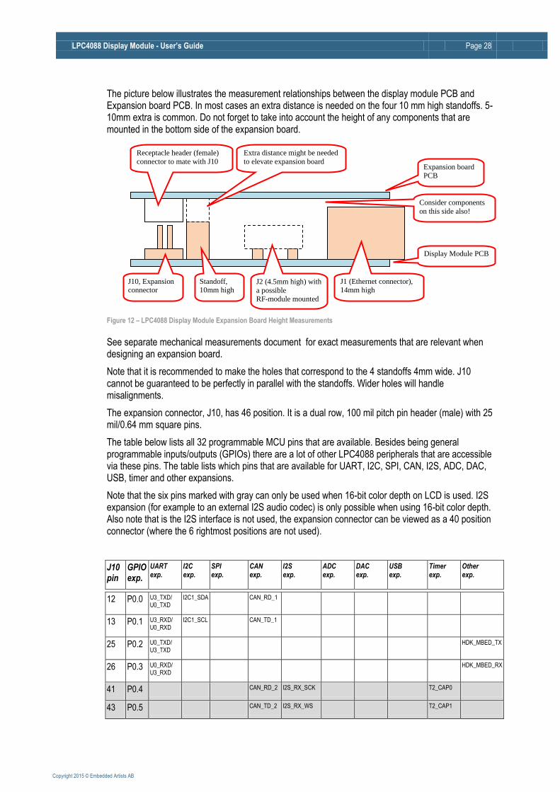
The picture below illustrates the measurement relationships between the display module PCB and Expansion board PCB. In most cases an extra distance is needed on the four 10 mm high standoffs. 5-10mm extra is common. Do not forget to take into account the height of any components that are mounted in the bottom side of the expansion board.
Figure 12 – LPC4088 Display Module Expansion Board Height Measurements
See separate mechanical measurements document for exact measurements that are relevant when designing an expansion board.
Note that it is recommended to make the holes that correspond to the 4 standoffs 4mm wide. J10 cannot be guaranteed to be perfectly in parallel with the standoffs. Wider holes will handle misalignments.
The expansion connector, J10, has 46 position. It is a dual row, 100 mil pitch pin header (male) with 25 mil/0.64 mm square pins.
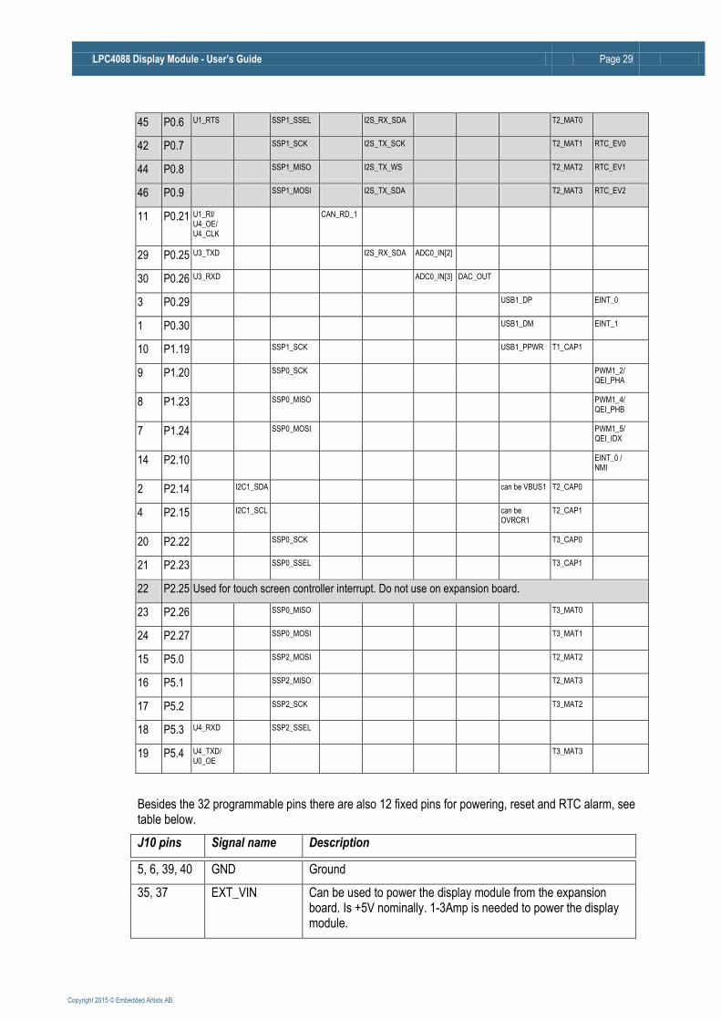
The table below lists all 32 programmable MCU pins that are available. Besides being general programmable inputs/outputs (GPIOs) there are a lot of other LPC4088 peripherals that are accessible via these pins. The table lists which pins that are available for UART, I2C, SPI, CAN, I2S, ADC, DAC, USB, timer and other expansions.
Note that the six pins marked with gray can only be used when 16-bit color depth on LCD is used. I2S expansion (for example to an external I2S audio codec) is only possible when using 16-bit color depth. Also note that is the I2S interface is not used, the expansion connector can be viewed as a 40 position connector (where the 6 rightmost positions are not used).
J10 pin
GPIO exp.
UART exp.
I2C exp.
SPI exp.
CAN exp.
I2S exp.
ADC exp.
DAC exp.
USB exp.
Timer exp.
Other exp.
12 P0.0 U3_TXD/
U0_TXD I2C1_SDA CAN_RD_1
13 P0.1 U3_RXD/ U0_RXD
I2C1_SCL CAN_TD_1
25 P0.2 U0_TXD/ U3_TXD
HDK_MBED_TX
26 P0.3 U0_RXD/ U3_RXD
HDK_MBED_RX
41 P0.4 CAN_RD_2 I2S_RX_SCK T2_CAP0
43 P0.5 CAN_TD_2 I2S_RX_WS T2_CAP1
J10, Expansion connector
Standoff, 10mm high
J2 (4.5mm high) with
a possible RF-module mounted
J1 (Ethernet connector), 14mm high
Expansion board
PCB
Display Module PCB
Consider components
on this side also!
Extra distance might be needed
to elevate expansion board Receptacle header (female)
connector to mate with J10
LPC4088 Display Module - User’s Guide Page 29
Copyright 2015 © Embedded Artists AB
45 P0.6 U1_RTS SSP1_SSEL I2S_RX_SDA T2_MAT0
42 P0.7 SSP1_SCK I2S_TX_SCK T2_MAT1 RTC_EV0
44 P0.8 SSP1_MISO I2S_TX_WS T2_MAT2 RTC_EV1
46 P0.9 SSP1_MOSI I2S_TX_SDA T2_MAT3 RTC_EV2
11 P0.21 U1_RI/ U4_OE/ U4_CLK
CAN_RD_1
29 P0.25 U3_TXD I2S_RX_SDA ADC0_IN[2]
30 P0.26 U3_RXD ADC0_IN[3] DAC_OUT
3 P0.29 USB1_DP EINT_0
1 P0.30 USB1_DM EINT_1
10 P1.19 SSP1_SCK USB1_PPWR T1_CAP1
9 P1.20 SSP0_SCK PWM1_2/ QEI_PHA
8 P1.23 SSP0_MISO PWM1_4/ QEI_PHB
7 P1.24 SSP0_MOSI PWM1_5/ QEI_IDX
14 P2.10 EINT_0 / NMI
2 P2.14 I2C1_SDA can be VBUS1 T2_CAP0
4 P2.15 I2C1_SCL can be OVRCR1
T2_CAP1
20 P2.22 SSP0_SCK T3_CAP0
21 P2.23 SSP0_SSEL T3_CAP1
22 P2.25 Used for touch screen controller interrupt. Do not use on expansion board.
23 P2.26 SSP0_MISO T3_MAT0
24 P2.27 SSP0_MOSI T3_MAT1
15 P5.0 SSP2_MOSI T2_MAT2
16 P5.1 SSP2_MISO T2_MAT3
17 P5.2 SSP2_SCK T3_MAT2
18 P5.3 U4_RXD SSP2_SSEL
19 P5.4 U4_TXD/ U0_OE
T3_MAT3
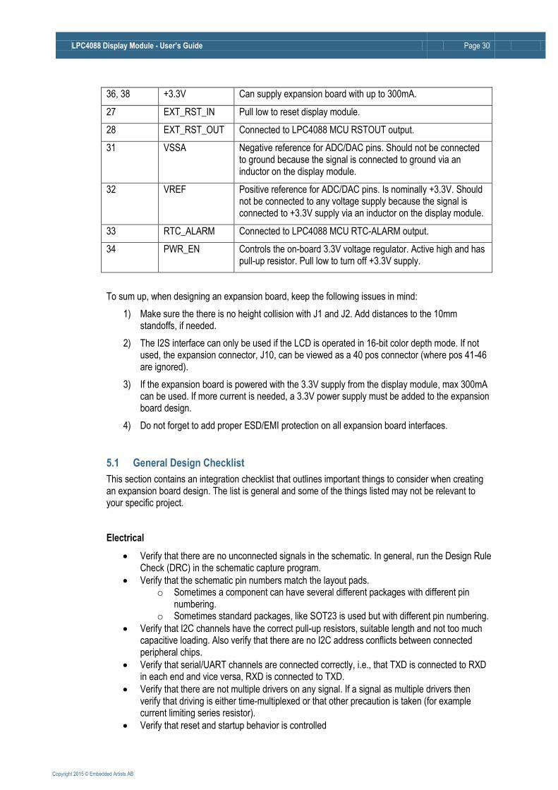
Besides the 32 programmable pins there are also 12 fixed pins for powering, reset and RTC alarm, see table below.
J10 pins Signal name Description
5, 6, 39, 40 GND Ground
35, 37 EXT_VIN Can be used to power the display module from the expansion board. Is +5V nominally. 1-3Amp is needed to power the display module.
LPC4088 Display Module - User’s Guide Page 30
Copyright 2015 © Embedded Artists AB
36, 38 +3.3V Can supply expansion board with up to 300mA.
27 EXT_RST_IN Pull low to reset display module.
28 EXT_RST_OUT Connected to LPC4088 MCU RSTOUT output.
31 VSSA Negative reference for ADC/DAC pins. Should not be connected to ground because the signal is connected to ground via an inductor on the display module.
32 VREF Positive reference for ADC/DAC pins. Is nominally +3.3V. Should not be connected to any voltage supply because the signal is connected to +3.3V supply via an inductor on the display module.
33 RTC_ALARM Connected to LPC4088 MCU RTC-ALARM output.
34 PWR_EN Controls the on-board 3.3V voltage regulator. Active high and has pull-up resistor. Pull low to turn off +3.3V supply.
To sum up, when designing an expansion board, keep the following issues in mind:
1) Make sure the there is no height collision with J1 and J2. Add distances to the 10mm standoffs, if needed.
2) The I2S interface can only be used if the LCD is operated in 16-bit color depth mode. If not used, the expansion connector, J10, can be viewed as a 40 pos connector (where pos 41-46 are ignored).
3) If the expansion board is powered with the 3.3V supply from the display module, max 300mA can be used. If more current is needed, a 3.3V power supply must be added to the expansion board design.
4) Do not forget to add proper ESD/EMI protection on all expansion board interfaces.
5.1 General Design Checklist
This section contains an integration checklist that outlines important things to consider when creating an expansion board design. The list is general and some of the things listed may not be relevant to your specific project.
Electrical
Verify that there are no unconnected signals in the schematic. In general, run the Design Rule Check (DRC) in the schematic capture program.
Verify that the schematic pin numbers match the layout pads. o Sometimes a component can have several different packages with different pin
numbering. o Sometimes standard packages, like SOT23 is used but with different pin numbering.
Verify that I2C channels have the correct pull-up resistors, suitable length and not too much capacitive loading. Also verify that there are no I2C address conflicts between connected peripheral chips.
Verify that serial/UART channels are connected correctly, i.e., that TXD is connected to RXD in each end and vice versa, RXD is connected to TXD.
Verify that there are not multiple drivers on any signal. If a signal as multiple drivers then verify that driving is either time-multiplexed or that other precaution is taken (for example current limiting series resistor).
Verify that reset and startup behavior is controlled

LPC4088 Display Module - User’s Guide Page 31
Copyright 2015 © Embedded Artists AB
o Correct output behavior of the system during reset and shortly after. o If nets have multiple drivers, verify that there are not multiple active drivers during
reset.
Verify that all I/O have proper ESD protection and suitable over-voltage/over-current protection, if needed.
Verify that all I/O have proper EMI (Electromagnetic Interference) protection - no disturbances are radiated and the I/O is immune to disturbances that can be expected (EMC - Electromagnetic Compatibility).
Specific for LPC4088 Display Module: Verify that signal P2.10 on the LPC4088 is not pulled low during/shortly after reset goes high. That will put the LPC4088 in ISP mode.
Powering
Verify that the output noise is low enough. o Specific to LPC4088 Display Module: The board expect less then +-50mV noise on
any power supply.
Verify that the power supply can deliver enough current in all situations (high temperature and low/high input voltage).
Verify that the step response of the power supply is acceptable. Make sure the verification is done in the complete operating temperature range. The step response of a power supply show how it behaves on a change in load current or input voltage. Verifying the step response ensures that the output voltage is always within the tolerances, even during transient conditions.
PCB
In general, consult your PCB layout partner for details about all the checklist points in this section.
Verify that all signals with special routing rules (for example USB signals) have been correctly specified with impedance requirements (differential or relative to ground) and other routing rules.
Verify that signals that carry large currents have the correct track widths and copper thickness.
Verify that the correct layout symbols have been used for all components. Many components have several different packages options. Sometimes datasheets refer to standard package names. These may not always have the same measures as the packages in the layout program library. Always double-check all components.
Verify that the board thickness, solder mask color, silk screen color and stackup are specified. The latter is extra important when there are signals need controlled impedance routing.
Verify that the layout is good from grounding, high speed signal, noise and disturbance perspectives. This subject is too big to just list in a few checkpoints. Check suitable application notes from silicon vendors or text books about the subject.
Physical/Mechanical
Verify that there is enough space around the module to be integrated. o A 3D model can be used to verify that the module (and the rest of the components in
the design) physically fits together.
Verify that an expansion board design will fit with the different components heights around the board.
Verify that the mounting holes on the expansion board are 4 mm wide. The extra width (M3 screws are used) will handle small misalignments of J10 (the expansion connector).
LPC4088 Display Module - User’s Guide Page 32
Copyright 2015 © Embedded Artists AB
Thermal
Verify that all components are specified and operate correctly in the full temperature range.
Verify that no component has too high power dissipation o Can for example the components dissipate max power without overheating? This is
mostly related to power supplies but can also be I/O protection circuits.
Other
Verify that the complete design can be tested effectively during production (Design for test).
Verify that the design is suitable for manufacturing (Design for manufacturing), for example PCB design rules, how (physically) close certain components are located, etc.
Verify that the Bill-of-Material (BOM) is completely specified and that components are available from suitable distributors in suitable volumes.
Verify that the selected components in the BOM have the correct RoHS status, or whatever environmental directive that needs to be adhered to.
Verify if the final product needs CE/FCC testing/certification.
LPC4088 Display Module - User’s Guide Page 33
Copyright 2015 © Embedded Artists AB
6 How to Embed / Integrate the Display Module This chapter presents the steps needed to integrate the LPC4088 Display Module into an end-product. There are a couple of steps to follow, as outlined in the following sections. The firmware/software side of the project is not addressed in this chapter. Only the electrical, mechanical and certification aspects.
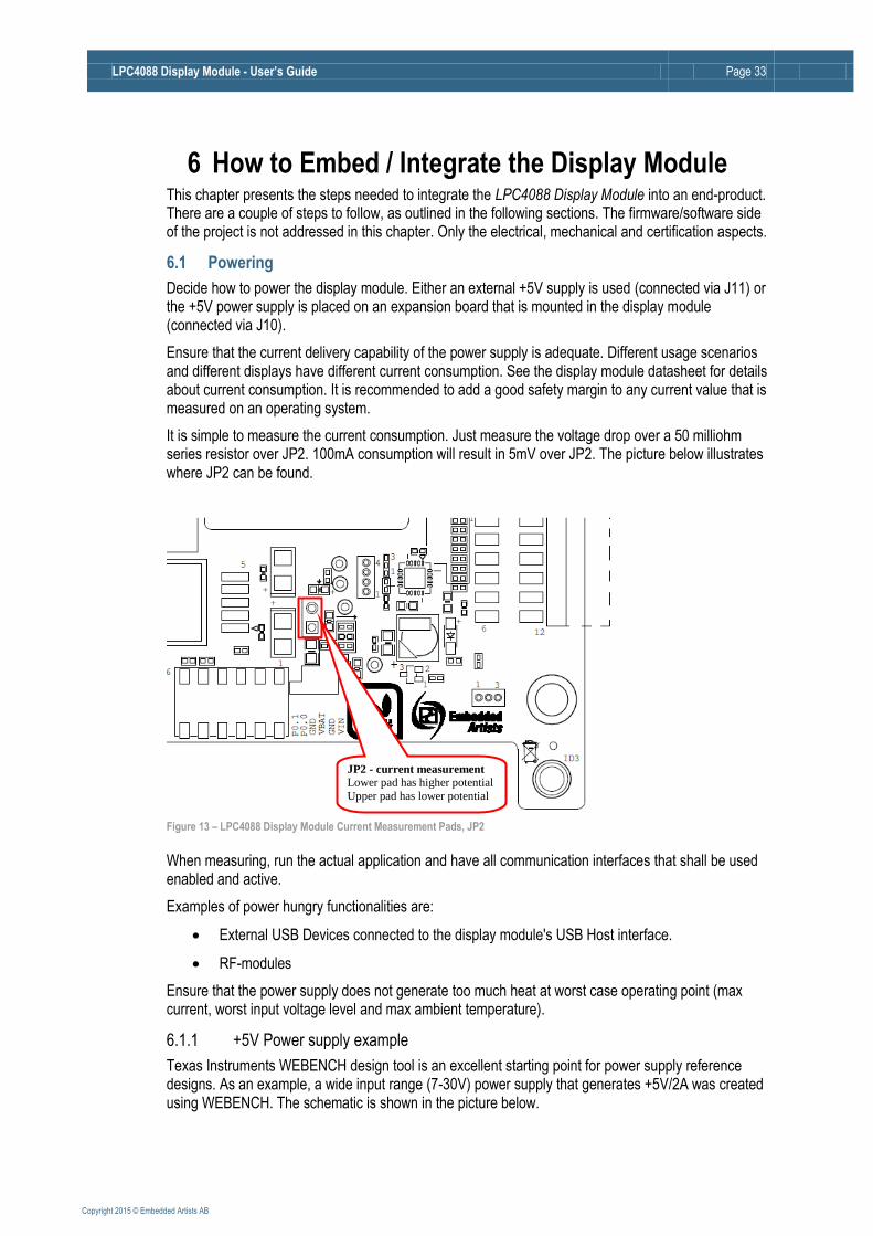
6.1 Powering
Decide how to power the display module. Either an external +5V supply is used (connected via J11) or the +5V power supply is placed on an expansion board that is mounted in the display module (connected via J10).
Ensure that the current delivery capability of the power supply is adequate. Different usage scenarios and different displays have different current consumption. See the display module datasheet for details about current consumption. It is recommended to add a good safety margin to any current value that is measured on an operating system.
It is simple to measure the current consumption. Just measure the voltage drop over a 50 milliohm series resistor over JP2. 100mA consumption will result in 5mV over JP2. The picture below illustrates where JP2 can be found.
Figure 13 – LPC4088 Display Module Current Measurement Pads, JP2
When measuring, run the actual application and have all communication interfaces that shall be used enabled and active.
Examples of power hungry functionalities are:
External USB Devices connected to the display module's USB Host interface.
RF-modules
Ensure that the power supply does not generate too much heat at worst case operating point (max current, worst input voltage level and max ambient temperature).
6.1.1 +5V Power supply example
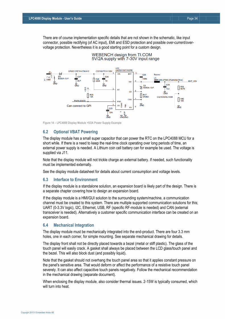
Texas Instruments WEBENCH design tool is an excellent starting point for power supply reference designs. As an example, a wide input range (7-30V) power supply that generates +5V/2A was created using WEBENCH. The schematic is shown in the picture below.
JP2 - current measurement
Lower pad has higher potential
Upper pad has lower potential
LPC4088 Display Module - User’s Guide Page 34
Copyright 2015 © Embedded Artists AB
There are of course implementation specific details that are not shown in the schematic, like input connector, possible rectifying (of AC input), EMI and ESD protection and possible over-current/over-voltage protection. Nevertheless it is a good starting point for a custom design.
Figure 14 – LPC4088 Display Module +5/2A Power Supply Example
6.2 Optional VBAT Powering
The display module has a small super capacitor that can power the RTC on the LPC4088 MCU for a short while. If there is a need to keep the real-time clock operating over long periods of time, an external power supply is needed. A Lithium coin cell battery can for example be used. The voltage is supplied via J11.
Note that the display module will not trickle charge an external battery. If needed, such functionality must be implemented externally.
See the display module datasheet for details about current consumption and voltage levels.
6.3 Interface to Environment
If the display module is a standalone solution, an expansion board is likely part of the design. There is a separate chapter covering how to design an expansion board.
If the display module is a HMI/GUI solution to the surrounding system/machine, a communication channel must be created to this system. There are multiple supported communication solutions for this; UART (0-3.3V logic), I2C, Ethernet, USB, RF (specific RF-module is needed) and CAN (external transceiver is needed). Alternatively a customer specific communication interface can be created on an expansion board.
6.4 Mechanical Integration
The display module must be mechanically integrated into the end-product. There are four 3.3 mm holes, one in each corner, for simple mounting. See separate mechanical drawing for details.
The display front shall not be directly placed towards a bezel (metal or stiff plastic). The glass of the touch panel will easily crack. A gasket shall always be placed between the LCD glass/touch panel and the bezel. This will also block dust (and possibly liquid).
Note that the gasket should not overhang the touch panel area so that it applies constant pressure on the panel's sensitive area. That would deform or affect the performance of a resistive touch panel severely. It can also affect capacitive touch panels negatively. Follow the mechanical recommendation in the mechanical drawing (separate document).
When enclosing the display module, also consider thermal issues. 2-15W is typically consumed, which will turn into heat.

LPC4088 Display Module - User’s Guide Page 35
Copyright 2015 © Embedded Artists AB
6.5 CE Declaration of Conformity
All electronic products put on the EU market must be CE marked. Depending on what the end-product is, there can be additional certification requirements.
As a standalone product, the LPC4088 Display Module is CE marked. The module has undergone EMC, EMI and ESD tests, see separate CE DoC (Declaration of Conformity) for details.
When integrating or embedding the LPC4088 Display Module in a final product new EMC, EMI and ESD tests must be done. This is especially true if an expansion board and/or a radio module is added to the design. The fact that the LPC4088 Display Module passes test as a standalone product increases the likelihood that the end-product also passes, but it is no guarantee.
6.6 Contact Embedded Artists
We recommend to contact Embedded Artists at an early stage in your project. We can offer a wide range of support during evaluation and the design-in phase.
The LPC4088 Display Module is well suited for many applications, like
Industrial controllers and HMI systems
Home automation and facility management
Audiovisual equipment
Instrumentation and measuring equipment
Vending machines
For more harsh use and environments, and where fail-safe operation, redundancy or other strict reliability or safety requirements exists, always contact Embedded Artists for a discussion about suitability.
There are application areas that the LPC4088 Display Module is not designed for (and such usage is strictly prohibited), for example:
Military equipment
Aerospace equipment
Control equipment for nuclear power industry
Medical equipment related to life support etc.
Gasoline stations and oil raffineries
If not before, it is essential to contact Embedded Artists before production begins. In order to ensure a reliable supply for you, as a customer, we need to know your production volume estimates and forecasts. Embedded Artists can typically provide smaller volumes of the display module directly from stock (for evaluation and prototyping), but larger volumes need to be planned.
The more information you can share with Embedded Artists about your plans, estimates and forecasts the higher the likelihood is that we can provide a reliable supply to you of the display module!

LPC4088 Display Module - User’s Guide Page 36
Copyright 2015 © Embedded Artists AB
7 Custom Specific Versions Embedded Artists offers a number of standard display module solutions that have been designed for typical application requirements. It is possible to create custom specific versions for applications with special requirements, even for modest volumes.
Things that can be changes are for example;
Which display that is mounted, i.e., display characteristics
o Other screen size
o Other pixel resolution
o Other backlight brightness
o Other viewing angles
o Other temperature range
o Other touch panel features
o External touch panel
o Other glass coating
Other mechanical design
Different memory configuration (more/less SDRAM and/or QSPI flash memory)
Other micro controller / application processor
If you do not find the exact display module version you need, please contact Embedded Artists for a discussion. There can be new modules being designed and possible 'early-adopter programs' that can be of interest.
Embedded Artists can also help with expansion board design for specific interfaces requirements.
Contact Embedded Artists at www.EmbeddedArtists.com or via [email protected] with your requests.

LPC4088 Display Module - User’s Guide Page 37
Copyright 2015 © Embedded Artists AB
8 Future Proof Design - BIOS One of the biggest challenges for a product like the LPC4088 Display Module is to get a reliable supply of LCDs. Displays have short product lifetime - that is just how it is. Similarly, the touch panel controllers (both resistive and capacitive) can become obsolete.
The LPC4088 Display Module has a unique future-proof design that separates the hardware specific code from the user code. The LPC4088 Display Module can change hardware design to the LCD, the LCD itself and touch panel controller without requiring the user code to be recompiled (with updated drivers).
The LPC4088 Display Module has a separate on-board memory that stores this hardware specific code - called BIOS code. This code contains LCD and touch panel initialization and interface functions to these functions blocks. The software framework around the BIOS code MUST be used in the user code. See the Software User Manual for details.
This also means that a specific LCD model on the LPC4088 Display Module is not sold, but rather an optical/visual specification. Embedded Artists can select to mount any LCD model as long as the datasheet and mechanical specifications are met.
A customer will be able to buy an LPC4088 Display Module years after the original design was done and the user code will (with very high likelihood) still run - even though the display and/or touch panel controller will likely not be the same as the original design.
If the BIOS memory content has accidentally been erased, see the LPC4088 Display Module Software Manual for instructions how to recover the content.

LPC4088 Display Module - User’s Guide Page 38
Copyright 2015 © Embedded Artists AB
9 Things to Note This chapter contains information that is worth noting when working with your LPC4088 Display Module.
9.1 Current Consumption and Limits of USB Ports
The current consumption for the LPC4088 Display Module can be close to what some USB Host port can supply. If the boards are powered from a USB Host port (for example a PC or laptop) and there are problems, like spontaneous resets or other strange things, it is likely that an external power supply is needed.
For more information about current consumption, see the LPC4088 Display Module datasheet.
9.2 CMSIS-DAP program download time
The on-board debugger is built around the mbed HDK functionality and is implemented on a resource limited MCU. The CMSIS-DAP interface performance is limited in speed. Flash download speed is about 10 kBytes / second (note that this number is just approximate and can differ between firmware versions).
By using an external, higher performance debug interface faster download times can be obtained. For example, the cheap (15 EUR), yet powerful LPC-Link2 debug probe will have about 20 kBytes / second in flash download time. This is about twice as fast as the on-board HDK debugger.
9.3 HDK USB Mass-storage does not work on Mac - LPC4088 locks up
The current version of the HDK is not compatible with how a Mac computer writes the binary file to the USB mass-storage device (that the HDK creates). If a Mac is used to download a binary file, the LPC4088 will be flashed with a partial binary that is in no way correct. When the LPC4088 starts executing this program it can lock up. Further, the HDK can give an error message (error file on the USB mass-storage device).
9.4 Cannot download binary to LPC4088 via Cortex Debug Connector
If it is impossible to download a new binary to the LPC4088 via an external debugger, it is likely that the LPC4088 is in a mode where it is impossible for the debugger to take control over it.
Press the user push-button while powering the board. That will place the LPC4088 is ISP/bootloader mode. After that it should be possible for the debugger to download a new binary.
9.5 Updating the HDK
It is a good idea to always have the latest version of the HDK firmware on the LPC4088 Display Module. The first step is to identify which HDK firmware version that is running.
Connect the LPC4088 Display Module to a computer to get the MBED drive and then open the mbed.htm file in an editor e.g. notepad (don't double click the file as it will launch a web browser and that will not help).
The file should look something like below (a version number, build date and release date - in this case it is the release from 2015-01-09). Note that the date should never be earlier than what is shown below.
<!-- mbed Microcontroller Website and Authentication Shortcut -->
<!-- Version: 0203 Build: Jan 9 2015 08:57:43 Git Commit SHA:
353477ad6adc89317bb6f12da887b3fd85c4c9ec Git local mods:No-->
<!-- This firmware is only to be used on LPC4088 DisplayModule board from Embedded Artists -->
<html>
<head>
<meta http-equiv="refresh" content="0; url=http://mbed.org/device/?code=..."/>
<title>mbed Website Shortcut</title>
</head>
<body></body>
</html>
LPC4088 Display Module - User’s Guide Page 39
Copyright 2015 © Embedded Artists AB
The latest firmware version is available from the product support on Embedded Artists website.
9.5.1 Update Procedure
Note that it is only possible to update the HDK firmware from a Windows PC. Linux or Mac will not work. The reason for this is limitations in the on-chip bootloader in the LPC11U35 (that implements the HDK debug interface).
1. Start by downloading the latest HDK firmware (from the LPC4088 Display Module support site)
2. Connect a USB cable to a Windows PC (just one end of the cable connected)
3. Press and hold down the RESET button on the LPC4088 Display Module
4. Insert the USB cable to the HDK micro-B USB connector, J9
5. Release the RESET button
6. A CRP_DISABLD drive should appear on the PC (if not unplug and redo steps 2, 3 and 4)
7. Delete the firmware.bin file from the CRP_DISABLD drive
8. Copy the binary downloaded in step 1 to the CRP_DISABLD drive
9. Disconnect and then connect the USB cable to get the normal MBED drive

LPC4088 Display Module - User’s Guide Page 40
Copyright 2015 © Embedded Artists AB
10 Troubleshooting This chapter contains information about how to troubleshoot a board that does not seem to operate properly. It is strongly advised to read through the list of tests and actions that can be done before contacting Embedded Artists. The different tests can help determine if there is a problem with the board, or not. For return policy, please read Embedded Artists’ General Terms and Conditions document (can be found at http://www.embeddedartists.com/shop/).
10.1 Powering
The first step is to make sure that powering works properly. Powering is described in section 3.3 .
1. Disconnect any external hardware connected to the LPC4088 Display Module, such as USB devices and RF modules.
2. Power the LPC4088 Display Module via the HDK micro-B USB connector (J9 - the mbed HDK connector).
Measure the +5V and +3.3V voltages with the help of the voltage measuring pads on the LPC4088 Display Module; TP7=+3.3V supply, TP8=5V supply, TP9=ground. Acceptable range for the +5V voltage is 4.4V to 5.5V. This is measured between TP8/TP9. Acceptable range for the +3.3V voltage is +3.15V to +3.45V. This is measured between TP7/TP9.
Figure 15 – LPC4088 Display Module TP7, TP8, TP9
If the reset-LED is dimming instead of being clearly on or off, it is also a sign that the supply voltages are not stable and outside of valid ranges.
3. Verify that there are no voltage dips on the supply. A typical indication of this is that the reset-LED flash from time to time. An oscilloscope can detect voltage dips; measure the supply voltage in AC mode. Set horizontal resolution to 50mV per square. Set the trigger to normal mode and adjust the trigger to 50mV below the normal level. That way, the oscilloscope will trigger every time a voltage dips occurs. By watching the dips it is possible to judge if there is a problem, or not.
4. Verify that the reset-LED flash when pressing the reset push-button. The LED should also light shortly after releasing the push button. The extra “LED on time” is very short but still noticeable (typically a 1/5 of a second, i.e., 200mS).
TP7: +3.3V
TP9: Ground
TP8: +5V TP10: VBAT

LPC4088 Display Module - User’s Guide Page 41
Copyright 2015 © Embedded Artists AB
5. In most cases it is possible to power the board via the micro-B USB (HDK) connector, but note that not all PC:s and/or laptops can power the board via their USB interfaces. In such cases, a USB hub with independent powering can work. Alternatively connect a stable DC supply (+5V) to main connector J11. Minimum current capability shall be 1A for this test. The noise level should be minimal, less than 50mV. Redo tests 3) to 5) above again.
10.2 Program Download to LPC4088
The second step is to make sure that it is possible to download an application (via the HDK) to the LPC4088. Follow these steps:
1. Connect a USB cable between the micro-B HDK USB connector and a PC running Windows.
2. In Windows, a drive (for example F:\) with the label “MBED” will appear.
3. Delete the file firmware.bin
4. Copy the pre-compiled binary file that is the test application. It can be downloaded from Embedded Artists' support page for the board.
5. When completed the HDK on the board will automatically restart and the MBED drive will appear again but without the file that was copied (the file has however been downloaded to the LPC4088).
6. Press reset to start the application.
10.3 Using Test Application to Verify Correct Operation
The third step is to utilize the just downloaded pre-compiled test application to verify correct operation of the board.
The network test requires a network that can handle DHCP (dynamic assignment of IP addresses). If your network does not support this then use a router and set it up to handle DHCP. All modern routers support this. Note that the tested board does not have to have network access to internet or any PC during testing – the only important thing is that it receives an IP address automatically.
Connect the Ethernet cable between the board and router.
Secondly, a FAT/FAT32 formatted uSD memory card must be prepared. Add a file, message.txt, in the root directory containing the following text:
eatest2014
Important that the first 10 characters are "eatest2014", the
rest does not matter!!!
Insert the prepared uSD/transflash memory card in the uSD connector.
Keep the USB cable in the mbed HDK connector so that the board is powered.
Connect a USB cable (mini-B to A) between J4 (mini-B USB connector) and a PC.
After this, start a terminal program in Windows with 9600 baud, 8-bit data, no parity, 1 stop bit and no flow control. Connect to the COM board that is created by the HDK.
Press the reset-button and make sure the test application greeting message can be seen in the terminal program.
1. Verify that the greeting message (from the test application) can be seen in the terminal program.
Production Test Program: LPC4088 Display Module
Build Date: ...
2. Test of real time clock. No interaction needed

LPC4088 Display Module - User’s Guide Page 42
Copyright 2015 © Embedded Artists AB
3. Test of SDRAM. No interaction needed
4. Test of QSPI memory. No interaction needed
5. Test of MCI interface to SD card. No interaction needed
6. Test of USB device. The tested board should appear in Windows as a USB memory stick. Make sure that a drive appears (e.g. H:\) and that there is a “image.png” file on it. Open the image file and make sure it looks like this:
7. Test of display in 24-bit mode. The same image as seen in step 6 above should appear on the display (it will be small but should look correct).
8. Test of backlight. Follow instructions in the terminal and press the button to increase the backlight in steps. Look at the display and make sure it gets brighter each time the button is pressed.
Testing display backlight...
backlight is 0%, press button to increase
backlight is 20%, press button to increase
backlight is 40%, press button to increase
backlight is 60%, press button to increase
backlight is 80%, press button to increase
backlight is 100%
9. Test of color bars. The display should show red, green and blue colors and they should fade between light and dark. If you look closely at the display the colors should be smooth like the left image below.
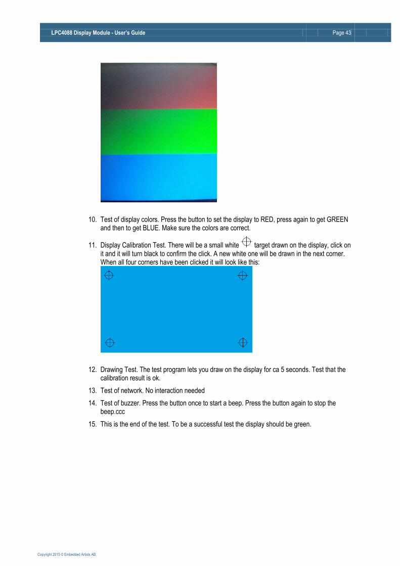
LPC4088 Display Module - User’s Guide Page 43
Copyright 2015 © Embedded Artists AB
10. Test of display colors. Press the button to set the display to RED, press again to get GREEN and then to get BLUE. Make sure the colors are correct.
11. Display Calibration Test. There will be a small white target drawn on the display, click on it and it will turn black to confirm the click. A new white one will be drawn in the next corner. When all four corners have been clicked it will look like this:
12. Drawing Test. The test program lets you draw on the display for ca 5 seconds. Test that the calibration result is ok.
13. Test of network. No interaction needed
14. Test of buzzer. Press the button once to start a beep. Press the button again to stop the beep.ccc
15. This is the end of the test. To be a successful test the display should be green.
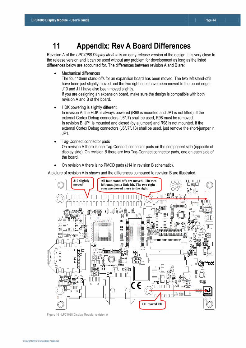
LPC4088 Display Module - User’s Guide Page 44
Copyright 2015 © Embedded Artists AB
11 Appendix: Rev A Board Differences Revision A of the LPC4088 Display Module is an early-release version of the design. It is very close to the release version and it can be used without any problem for development as long as the listed differences below are accounted for. The differences between revision A and B are:
Mechanical differences The four 10mm stand-offs for an expansion board has been moved. The two left stand-offs have been just slightly moved and the two right ones have been moved to the board edge. J10 and J11 have also been moved slightly. If you are designing an expansion board, make sure the design is compatible with both revision A and B of the board.
HDK powering is slightly different. In revision A, the HDK is always powered (R98 is mounted and JP1 is not fitted). If the external Cortex Debug connectors (J6/J7) shall be used, R98 must be removed. In revision B, JP1 is mounted and closed (by a jumper) and R98 is not mounted. If the external Cortex Debug connectors (J6/J7/J13) shall be used, just remove the short-jumper in JP1.
Tag-Connect connector pads On revision A there is one Tag-Connect connector pads on the component side (opposite of display side). On revision B there are two Tag-Connect connector pads, one on each side of the board.
On revision A there is no PMOD pads (J14 in revision B schematic).
A picture of revision A is shown and the differences compared to revision B are illustrated.
Figure 16 –LPC4088 Display Module, revision A
J10 slightly
moved All four stand-offs are moved. The two
left ones, just a little bit. The two right
ones are moved more to the right.
J11 moved left
LPC4088 Display Module - User’s Guide Page 45
Copyright 2015 © Embedded Artists AB
12 Further Information The LPC4088 microcontroller is a complex circuit and there exist a number of other documents with a lot more information. The following documents are recommended as a complement to this document.
[1] NXP LPC4088 Datasheet http://www.nxp.com/documents/data_sheet/LPC408X_7X.pdf
[2] NXP LPC4088 User’s Manual http://www.nxp.com/documents/user_manual/UM10562.pdf
[3] NXP LPC4088 Errata http://www.nxp.com/documents/errata_sheet/ES_LPC407X_8X.pdf
[4] ARM Processor Documentation Documentation from ARM can be found at: http://infocenter.arm.com/.
[5] Information on different ARM Architectures http://www.arm.com/products/processors/technologies/ instruction-set-architectures.php
[6] ARMv7-M Architecture Reference Manual. Document identity: DDI 0403D http://infocenter.arm.com/help/index.jsp?topic=/com.arm.doc.ddi0403c/index.html
[7] Cortex-M4 Technical Reference Manual. Revision: r0p1 http://infocenter.arm.com/help/index.jsp?topic=/com.arm.doc.ddi0439c/index.html
[8] LPCware, NXP's community for developers http://www.lpcware.com/
[9] LPCXpresso IDE: NXP's low-cost development platform for LPC families, which is an Eclipse-based IDE. http://www.lpcware.com/lpcxpresso
[10] LPCOpen - a Software Development Platform for NXP's LPC Microcontrollers http://www.lpcware.com/lpcopen
[11] mbed.org, the official site for mbed development and gives access to all documentation and the on-line compiler. http://mbed.org
Note that there can be newer versions of the documents than the ones linked to here. Always check for the latest information/version.