lt1028/lt1128 - ultralow noise precision high speed op amps
TRANSCRIPT

LT1028/LT1128
11028fd
For more information www.linear.com/LT1028
TYPICAL APPLICATION
FEATURES DESCRIPTION
Ultralow Noise PrecisionHigh Speed Op Amps
The LT®1028(gain of –1 stable)/LT1128(gain of +1 stable) achieve a new standard of excellence in noise performance with 0.85nV/√Hz 1kHz noise, 1.0nV/√Hz 10Hz noise. This ultralow noise is combined with excellent high speed specifications (gain-bandwidth product is 75MHz for LT1028, 20MHz for LT1128), distortion-free output, and true precision parameters (0.1µV/°C drift, 10µV offset voltage, 30 million voltage gain). Although the LT1028/LT1128 input stage operates at nearly 1mA of collector current to achieve low voltage noise, input bias current is only 25nA.
The LT1028/LT1128’s voltage noise is less than the noise of a 50Ω resistor. Therefore, even in very low source impedance transducer or audio amplifier applications, the LT1028/LT1128’s contribution to total system noise will be negligible.L, LT, LTC, LTM, Linear Technology and the Linear logo are registered trademarks of Linear Technology Corporation. All other trademarks are the property of their respective owners.
Ultralow Noise 1M TIA Photodiode Amplifier
APPLICATIONS
n Voltage Noise 1.1nV/√Hz Max at 1kHz 0.85nV/√Hz Typ at 1kHz 1.0nV/√Hz Typ at 10Hz 35nVP-P Typ, 0.1Hz to 10Hzn Voltage and Current Noise 100% Testedn Gain-Bandwidth Product LT1028: 50MHz Min LT1128: 13MHz Minn Slew Rate LT1028: 11V/µs Min LT1128: 5V/µs Minn Offset Voltage: 40µV Maxn Drift with Temperature: 0.8µV/°C Maxn Voltage Gain: 7 Million Minn Available in 8-Lead SO Package
n Low Noise Frequency Synthesizersn High Quality Audion Infrared Detectorsn Accelerometer and Gyro Amplifiersn 350Ω Bridge Signal Conditioningn Magnetic Search Coil Amplifiersn Hydrophone Amplifiers
Voltage Noise vs Frequency
FREQUENCY (Hz)1
0.1
1
10
10 100
1028 TA02
VOLT
AGE
NOIS
E DE
NSIT
Y (n
V/√H
z)
0.1 1k
1/f CORNER = 3.5Hz
1/f CORNER = 14Hz
TYPICAL
MAXIMUM
VS = 15VTA = 25°C
+
– VOUT = ~0.4V + IPD • 1M
VS–
VS–
VS+
LT1028
0.1µF
JFETNXPBF862
PHOTODIODESFH213
D
S
4.32k
1028 TA01
1M
0.5pF
4.99k
VS = ±15V

LT1028/LT1128
21028fd
For more information www.linear.com/LT1028
ABSOLUTE MAXIMUM RATINGS
Supply Voltage –55°C to 105°C .................................................. ±22V 105°C to 125°C .................................................. ±16VDifferential Input Current (Note 9) .......................±25mAInput Voltage ..............................Equal to Supply VoltageOutput Short-Circuit Duration .......................... Indefinite
(Note 1)
TOP VIEW
V+
VOS TRIM
–IN OUT
OVER-COMP
+IN
V–
(CASE)
87
53
2
1
4
H PACKAGE8-LEAD TO-5 METAL CAN
VOS TRIM
+
–6
TJMAX = 175°C, θJA = 140°C/W, θJC = 40°C/W
OBSOLETE PACKAGE
1
2
3
4 5
6
7
8
TOP VIEW
–IN
+IN
V–
S8 PACKAGE8-LEAD PLASTIC SOIC
V+
OUT+
–
VOSTRIM
VOSTRIM
OVER-COMP
TJMAX = 150°C, θJA = 140°C/W
N8 PACKAGE8-LEAD PLASTIC DIP
1
2
3
4 5
6
7
8
TOP VIEW
–IN
+IN
V–
V+
OUT+
–
OVER-COMP
VOSTRIM
VOSTRIM
TJMAX = 150°C, θJA = 150°C/W
TOP VIEW
SW PACKAGE16-LEAD PLASTIC SOL
1
2
3
4
5
6
7
8
16
15
14
13
12
11
10
9
NC
NC
TRIM
–IN
+IN
V–
NC
NC
NC
NC
TRIM
V+
OUT
NC
NC
OVER-COMP
+
–
TJMAX = 150°C, θJA = 130°C/W
NOTE: THIS DEVICE IS NOT RECOMMENDED FOR NEW DESIGNS
J8 PACKAGE8-LEAD CERAMIC DIP
TJMAX = 175°C, θJA = 140°C/W, θJC = 40°C/W
OBSOLETE PACKAGE
PIN CONFIGURATION
Operating Temperature Range LT1028/LT1128AM, M (OBSOLETE) ... –55°C to 125°C LT1028/LT1128AC, C (Note 11) ............–40°C to 85°CStorage Temperature Range All Devices ......................................... –65°C to 150°CLead Temperature (Soldering, 10 sec.) .................. 300°C

LT1028/LT1128
31028fd
For more information www.linear.com/LT1028
ORDER INFORMATIONLEAD FREE FINISH TAPE AND REEL PART MARKING* PACKAGE DESCRIPTION SPECIFIED TEMPERATURE RANGE
LT1028ACN8#PBF N/A LT1028ACN8 8-Lead PDIP 0°C to 70°C
LT1028CN8#PBF N/A LT1028CN8 8-Lead PDIP 0°C to 70°C
LT1128ACN8#PBF N/A LT1128ACN8 8-Lead PDIP 0°C to 70°C
LT1128CN8#PBF N/A LT1128CN8 8-Lead PDIP 0°C to 70°C
LT1028CS8#PBF LT1028CS8#TRPBF 1028 8-Lead Plastic Small Outline 0°C to 70°C
LT1128CS8#PBF LT1128CS8#TRPBF 1128 8-Lead Plastic Small Outline 0°C to 70°C
LT1028CSW#PBF LT1028CSW#TRPBF LT1028CSW 16-Lead Plastic SOIC (Wide) 0°C to 70°C
Consult LTC Marketing for parts specified with wider operating temperature ranges. *The temperature grade is identified by a label on the shipping container.For more information on lead free part marking, go to: http://www.linear.com/leadfree/ For more information on tape and reel specifications, go to: http://www.linear.com/tapeandreel/. Some packages are available in 500 unit reels through designated sales channels with #TRMPBF suffix.
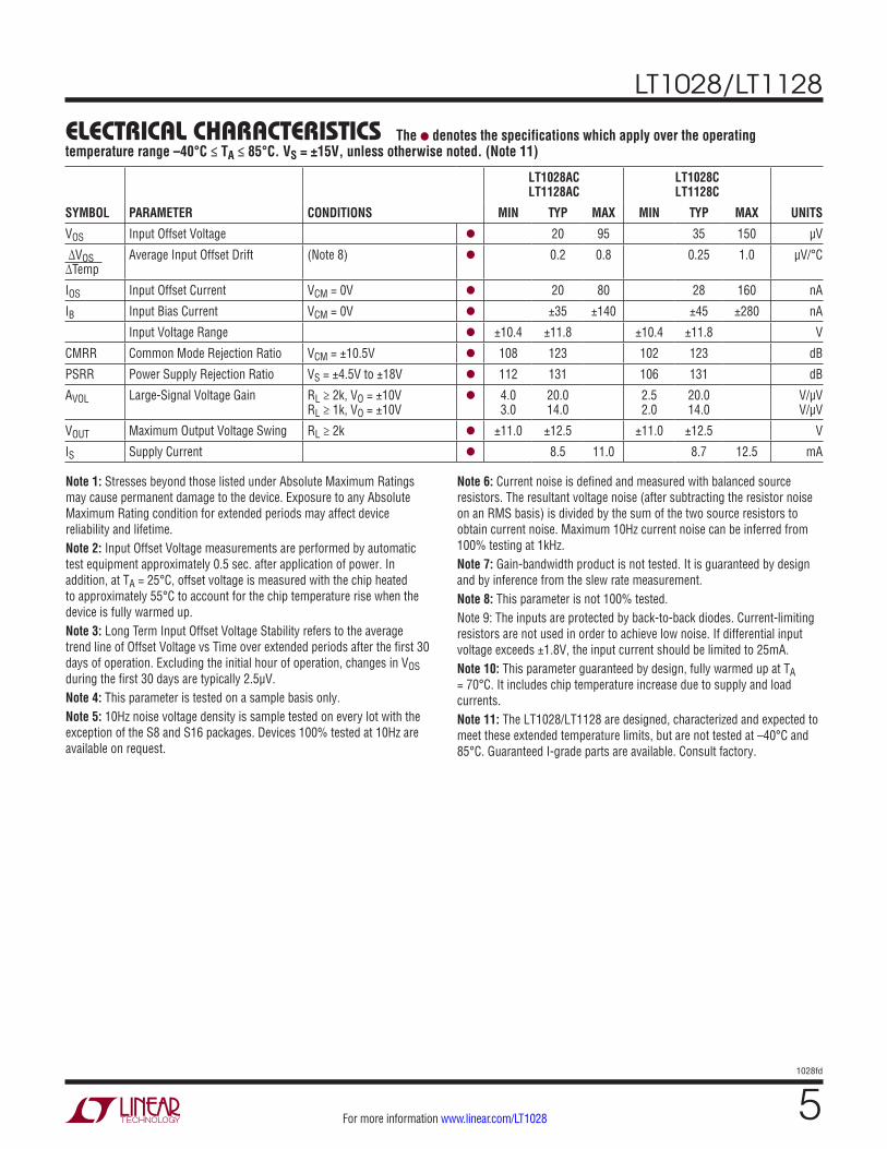
ELECTRICAL CHARACTERISTICS VS = ±15V, TA = 25°C unless otherwise noted.
LT1028AM/AC LT1128AM/AC
LT1028M/C LT1128M/C
SYMBOL PARAMETER CONDITIONS MIN TYP MAX MIN TYP MAX UNITSVOS Input Offset Voltage (Note 2) 10 40 20 80 µV ∆VOS ∆Time
Long Term Input Offset Voltage Stability
(Note 3) 0.3 0.3 µV/Mo
IOS Input Offset Current VCM = 0V 12 50 18 100 nAIB Input Bias Current VCM = 0V ±25 ±90 ±30 ±180 nAen Input Noise Voltage 0.1Hz to 10Hz (Note 4) 35 75 35 90 nVP-P
Input Noise Voltage Density fO = 10Hz (Note 5) fO = 1000Hz, 100% Tested
1.00 0.85
1.7 1.1
1.0 0.9
1.9 1.2
nV/√Hz nV/√Hz
In Input Noise Current Density fO = 10Hz (Notes 4 and 6) fO = 1000Hz, 100% Tested
4.7 1.0
10.0 1.6
4.7 1.0
12.0 1.8
pA/√Hz pA/√Hz
Input Resistance Common Mode Differential Mode
300 20
300 20
MΩ kΩ
Input Capacitance 5 5 pFInput Voltage Range ±11.0 ±12.2 ±11.0 ±12.2 V
CMRR Common Mode Rejection Ratio VCM = ±11V 114 126 110 126 dBPSRR Power Supply Rejection Ratio VS = ±4V to ±18V 117 133 110 132 dBAVOL Large-Signal Voltage Gain RL ≥ 2k, VO = ±12V
RL ≥ 1k, VO = ±10V RL ≥ 600Ω, VO = ±10V
7.0 5.0 3.0
30.0 20.0 15.0
5.0 3.5 2.0
30.0 20.0 15.0
V/µV V/µV V/µV
VOUT Maximum Output Voltage Swing RL ≥ 2k RL ≥ 600Ω
±12.3 ±11.0
±13.0 ±12.2
±12.0 ±10.5
±13.0 ±12.2
V V
SR Slew Rate AVCL = –1 LT1028 AVCL = –1 LT1128
11.0 5.0
15.0 6.0
11.0 4.5
15.0 6.0
V/µs V/µs
GBW Gain-Bandwidth Product fO = 20kHz (Note 7) LT1028 fO = 200kHz (Note 7) LT1128
50 13
75 20
50 11
75 20
MHz MHz
ZO Open-Loop Output Impedance VO = 0, IO = 0 80 80 ΩIS Supply Current 7.4 9.5 7.6 10.5 mA

LT1028/LT1128
41028fd
For more information www.linear.com/LT1028
ELECTRICAL CHARACTERISTICS
The l denotes the specifications which apply over the operating temperature range 0°C ≤ TA ≤ 70°C. VS = ±15V, unless otherwise noted.
LT1028AC LT1128AC
LT1028C LT1128C
SYMBOL PARAMETER CONDITIONS MIN TYP MAX MIN TYP MAX UNITS
VOS Input Offset Voltage (Note 2) l 15 80 30 125 µV
∆VOS ∆Temp
Average Input Offset Drift (Note 8) l 0.1 0.8 0.2 1.0 µV/°C
IOS Input Offset Current VCM = 0V l 15 65 22 130 nA
IB Input Bias Current VCM = 0V l ±30 ±120 ±40 ±240 nA
Input Voltage Range l ±10.5 ±12.0 ±10.5 ±12.0 V
CMRR Common Mode Rejection Ratio VCM= ±10.5V l 110 124 106 124 dB
PSRR Power Supply Rejection Ratio VS = ±4.5V to ±18V l 114 132 107 132 dB
AVOL Large-Signal Voltage Gain RL ≥ 2k, VO = ±10V RL ≥ 1k, VO = ±10V
l 5.0 4.0
25.0 18.0
3.0 2.5
25.0 18.0
V/µV V/µV
VOUT Maximum Output Voltage Swing RL ≥ 2k RL ≥ 600Ω (Note 10)
l ±11.5 ±9.5
±12.7 ±11.0
±11.5 ±9.0
±12.7 ±10.5
V V
IS Supply Current l 8.0 10.5 8.2 11.5 mA
The l denotes the specifications which apply over the operating temperature range –55°C ≤ TA ≤ 125°C. VS = ±15V, unless otherwise noted.
LT1028AM LT1128AM
LT1028M LT1128M
SYMBOL PARAMETER CONDITIONS MIN TYP MAX MIN TYP MAX UNITSVOS Input Offset Voltage (Note 2) l 30 120 45 180 µV ∆VOS ∆Temp
Average Input Offset Drift (Note 8) l 0.2 0.8 0.25 1.0 µV/°C
IOS Input Offset Current VCM = 0V l 25 90 30 180 nAIB Input Bias Current VCM = 0V l ±40 ±150 ±50 ±300 nA
Input Voltage Range l ±10.3 ±11.7 ±10.3 ±11.7 VCMRR Common Mode Rejection Ratio VCM = ±10.3V l 106 122 100 120 dBPSRR Power Supply Rejection Ratio VS = ±4.5V to ±16V l 110 130 104 130 dBAVOL Large-Signal Voltage Gain RL ≥ 2k, VO = ±10V
RL ≥ 1k, VO = ±10Vl 3.0
2.014.0 10.0
2.0 1.5
14.0 10.0
V/µV V/µV
VOUT Maximum Output Voltage Swing RL ≥ 2k l ±10.3 ±11.6 ±10.3 ±11.6 VIS Supply Current l 8.7 11.5 9.0 13.0 mA
LT1028/LT1128
51028fd
For more information www.linear.com/LT1028
LT1028AC LT1128AC
LT1028C LT1128C
SYMBOL PARAMETER CONDITIONS MIN TYP MAX MIN TYP MAX UNITS
VOS Input Offset Voltage l 20 95 35 150 µV
∆VOS ∆Temp
Average Input Offset Drift (Note 8) l 0.2 0.8 0.25 1.0 µV/°C
IOS Input Offset Current VCM = 0V l 20 80 28 160 nA
IB Input Bias Current VCM = 0V l ±35 ±140 ±45 ±280 nA
Input Voltage Range l ±10.4 ±11.8 ±10.4 ±11.8 V
CMRR Common Mode Rejection Ratio VCM = ±10.5V l 108 123 102 123 dB
PSRR Power Supply Rejection Ratio VS = ±4.5V to ±18V l 112 131 106 131 dB
AVOL Large-Signal Voltage Gain RL ≥ 2k, VO = ±10V RL ≥ 1k, VO = ±10V
l 4.0 3.0
20.0 14.0
2.5 2.0
20.0 14.0
V/µV V/µV
VOUT Maximum Output Voltage Swing RL ≥ 2k l ±11.0 ±12.5 ±11.0 ±12.5 V
IS Supply Current l 8.5 11.0 8.7 12.5 mA
The l denotes the specifications which apply over the operating temperature range –40°C ≤ TA ≤ 85°C. VS = ±15V, unless otherwise noted. (Note 11)
Note 1: Stresses beyond those listed under Absolute Maximum Ratings may cause permanent damage to the device. Exposure to any Absolute Maximum Rating condition for extended periods may affect device reliability and lifetime.Note 2: Input Offset Voltage measurements are performed by automatic test equipment approximately 0.5 sec. after application of power. In addition, at TA = 25°C, offset voltage is measured with the chip heated to approximately 55°C to account for the chip temperature rise when the device is fully warmed up.Note 3: Long Term Input Offset Voltage Stability refers to the average trend line of Offset Voltage vs Time over extended periods after the first 30 days of operation. Excluding the initial hour of operation, changes in VOS during the first 30 days are typically 2.5µV.Note 4: This parameter is tested on a sample basis only.Note 5: 10Hz noise voltage density is sample tested on every lot with the exception of the S8 and S16 packages. Devices 100% tested at 10Hz are available on request.
Note 6: Current noise is defined and measured with balanced source resistors. The resultant voltage noise (after subtracting the resistor noise on an RMS basis) is divided by the sum of the two source resistors to obtain current noise. Maximum 10Hz current noise can be inferred from 100% testing at 1kHz.Note 7: Gain-bandwidth product is not tested. It is guaranteed by design and by inference from the slew rate measurement.Note 8: This parameter is not 100% tested.Note 9: The inputs are protected by back-to-back diodes. Current-limiting resistors are not used in order to achieve low noise. If differential input voltage exceeds ±1.8V, the input current should be limited to 25mA.Note 10: This parameter guaranteed by design, fully warmed up at TA = 70°C. It includes chip temperature increase due to supply and load currents.Note 11: The LT1028/LT1128 are designed, characterized and expected to meet these extended temperature limits, but are not tested at –40°C and 85°C. Guaranteed I-grade parts are available. Consult factory.
ELECTRICAL CHARACTERISTICS
LT1028/LT1128
61028fd
For more information www.linear.com/LT1028
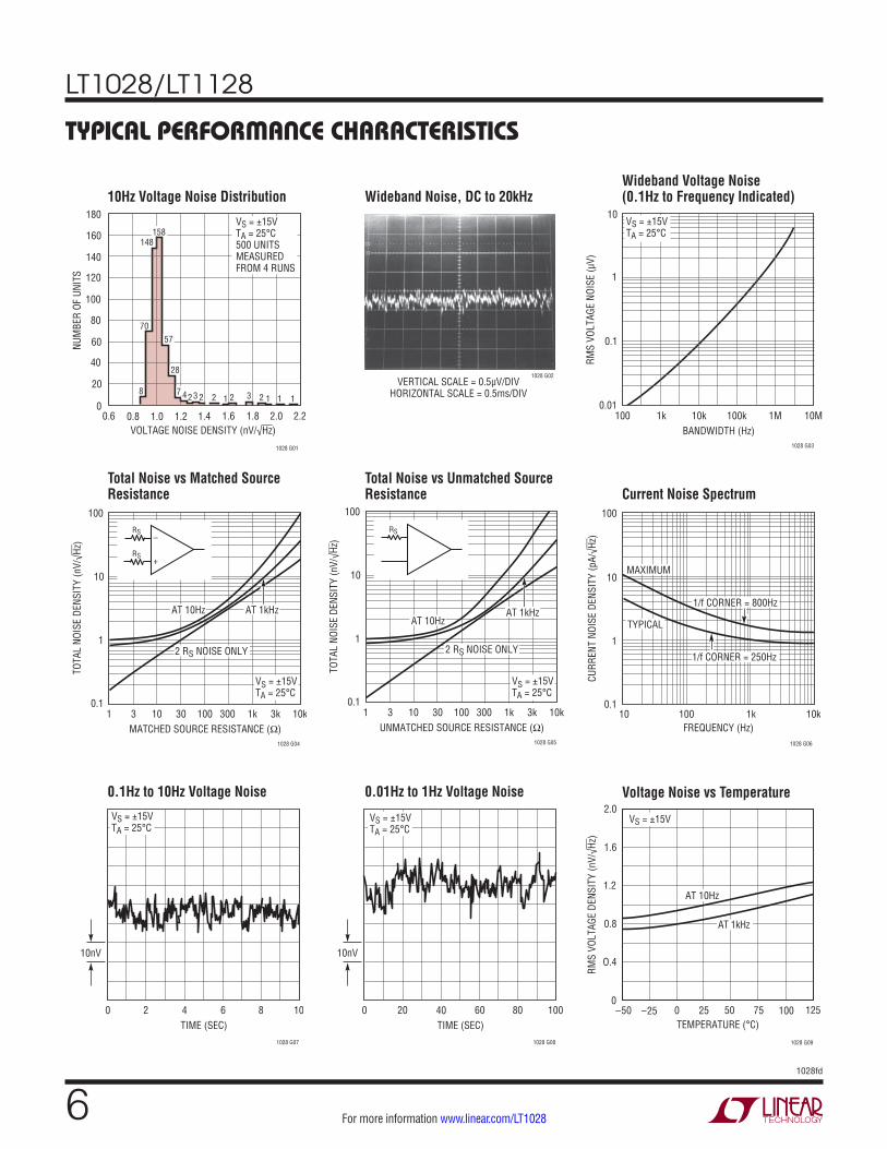
TYPICAL PERFORMANCE CHARACTERISTICS
10Hz Voltage Noise Distribution
Total Noise vs Matched Source Resistance
Total Noise vs Unmatched Source Resistance Current Noise Spectrum
0.01Hz to 1Hz Voltage Noise Voltage Noise vs Temperature0.1Hz to 10Hz Voltage Noise
Wideband Noise, DC to 20kHzWideband Voltage Noise(0.1Hz to Frequency Indicated)
0.60
NUM
BER
OF U
NITS
20
60
80
100
1.0 1.4 1.8
180
1028 G01
40
0.8 1.2
120
140
160
1.6 2.0 2.2
8
70
148158
57
28
7 423 2 2 21 3 2 1 1 1
VS = ±15VTA = 25°C500 UNITSMEASUREDFROM 4 RUNS
VOLTAGE NOISE DENSITY (nV/√Hz)
1028 G02VERTICAL SCALE = 0.5µV/DIV
HORIZONTAL SCALE = 0.5ms/DIV
BANDWIDTH (Hz)100
RMS
VOLT
AGE
NOIS
E (µ
V)
0.1
1
100k 1M 10M
1028 G03
0.01
10
10k1k
VS = ±15VTA = 25°C
MATCHED SOURCE RESISTANCE (Ω)1
TOTA
L NO
ISE
DENS
ITY
(nV/
√Hz)
10
100
3 1k 10k
1028 G04
1
0.1
VS = ±15VTA = 25°C
10 30 100 300 3k
AT 10Hz
2 RS NOISE ONLY
AT 1kHz
–
+
RS
RS
UNMATCHED SOURCE RESISTANCE (Ω)1
TOTA
L NO
ISE
DENS
ITY
(nV/
√Hz)
10
100
3 1k 10k
1028 G05
1
0.1
VS = ±15VTA = 25°C
10 30 100 300 3k
AT 10Hz
2 RS NOISE ONLY
AT 1kHz
RS
FREQUENCY (Hz)10
0.1
CURR
ENT
NOIS
E DE
NSIT
Y (p
A/√H
z)
1
10
100
100 1k 10k
1028 G06
MAXIMUM
TYPICAL
1/f CORNER = 800Hz
1/f CORNER = 250Hz
TIME (SEC)0 8
1028 G07
2 4 6 10
10nV
VS = ±15VTA = 25°C
TIME (SEC)0 80
1028 G08
20 40 60 100
10nV
VS = ±15VTA = 25°C
TEMPERATURE (°C)–50
0
RMS
VOLT
AGE
DENS
ITY
(nV/
√Hz)
0.8
2.0
0 50 75
1028 G09
O.4
1.6
1.2
–25 25 100 125
VS = ±15V
AT 10Hz
AT 1kHz

LT1028/LT1128
71028fd
For more information www.linear.com/LT1028
TYPICAL PERFORMANCE CHARACTERISTICS
Supply Current vs TemperatureVoltage Noise vs Supply Voltage
Bias Current Over the Common Mode RangeWarm-Up Drift
Output Short-Circuit Currentvs Time
Distribution of Input Offset Voltage
Input Bias and Offset Currents Over Temperature
Long-Term Stability of Five Representative Units
Offset Voltage Drift with Temperature of Representative Units
OFFSET VOLTAGE (µV)–50
UNIT
S (%
) 12
16
20
30
1028 G10
8
4
0–30 –10 10 50
10
14
18
6
2
20–40 –20 0 40
VS = ±15VTA = 25°C800 UNITS TESTEDFROM FOUR RUNS
TEMPERATURE (°C)–50
–50
OFFS
ET V
OLTA
GE (µ
V)
–40
–20
–10
0
50
20
0 50 75
1028 G11
–30
30
40
10
–25 25 100 125
VS = ±15V
TIME (MONTHS)0
OFFS
ET V
OLTA
GE C
HANG
E (µ
V)
2
6
10
4
1028 G12
–2
–6
–101 2 3 5
0
4
8
–4
–8
VS = ±15VTA = 25°Ct = 0 AFTER 1 DAY PRE-WARM UP
TIME AFTER POWER ON (MINUTES)0
0
CHAN
GE IN
OFF
SET
VOLT
AGE
(µV)
4
8
12
16
20
24
1 2 3 4
1028 G13
5
VS = ±15VTA = 25°C
METAL CAN (H) PACKAGE
DUAL-IN-LINE PACKAGEPLASTIC (N) OR CERDIP (J)
TEMPERATURE (°C)–50
INPU
T BI
AS A
ND O
FFSE
T CU
RREN
TS (n
A)
40
50
60
25 75
1028 G14
30
20
–25 0 50 100 125
10
0
VS = ±15VVCM = 0V
BIAS CURRENT
OFFSET CURRENT
COMMON MODE INPUT VOLTAGE (V)–15
–80
INPU
T BI
AS C
URRE
NT (n
A)
–60
–20
0
20
–5 5 15
100
1028 G15
–40
–10 0
40
60
80
10
RCM = 20V65nA
ª 300MΩ VS = ±15VTA = 25°C
POSITIVE INPUT CURRENT(UNDERCANCELLED) DEVICE
NEGATIVE INPUT CURRENT(OVERCANCELLED) DEVICE
TEMPERATURE (°C)–50
0
SUPP
LY C
URRE
NT (m
A)
1
3
4
5
10
7
0 50 75
1028 G17
2
8
9
6
–25 25 100 125
VS = ±15V
VS = ±5V
TIME FROM OUTPUT SHORT TO GROUND (MINUTES)0
–50
SINK
ING
–40
–20
–10
0
50
20
2
1028 G18
–30
30
40
10
1 3
SHOR
T-CI
RCUI
T CU
RREN
T (m
A)SO
URCI
NG
VS = ±15V–50°C25°C
125°C
–50°C
125°C
25°C
SUPPLY VOLTAGE (V)0
RMS
VOLT
AGE
NOIS
E DE
NSIT
Y (n
V/√H
z)
1.0
1.25
±15
1028 G16
0.75
0.5±5 ±10 ±20
1.5TA = 25°C
AT 10Hz
AT 1kHz

LT1028/LT1128
81028fd
For more information www.linear.com/LT1028
TYPICAL PERFORMANCE CHARACTERISTICS
Gain Error vs FrequencyClosed-Loop Gain = 1000
LT1128Gain Phase vs Frequency
LT1028Gain, Phase vs FrequencyVoltage Gain vs Frequency
Voltage Gain vs Supply Voltage Voltage Gain vs Load ResistanceMaximum Undistorted Outputvs Frequency
LT1128Capacitance Load Handling
LT1028Capacitance Load Handling
FREQUENCY (Hz)0.01
–20
VOLT
AGE
GAIN
(dB)
160
1028 G19
140
120
100
80
60
40
20
0
0.1 1 10 100 1k 10k 100k 1M 10M 100M
LT1128 LT1028
VS = ±15VTA = 25°CRL = 2k
FREQUENCY (Hz)
10
VOLT
AGE
GAIN
(dB)
20
40
50
70
10k 1M 10M 100M
1028 G20
–10100k
60
30
0VS = ±15VTA = 25°CCL = 10pF
GAIN
PHASE
10
20
40
50
70
–10
60
30
0
PHAS
E M
ARGI
N (D
EG)
CAPACITIVE LOAD (pF)10
40
OVER
SHOO
T (%
)
50
60
70
80
100 1000 10000
1028 G21
30
20
10
0
VS = ±15VTA = 25°C
–
+CL
2k
30pF
RS
AV = –1, RS = 2k
AV = –100RS = 20Ω
AV = –10RS = 200Ω
FREQUENCY (Hz)0.1
0.001
GAIN
ERR
OR (%
)
0.01
0.1
1
1 100
1028 G22
LT1128
LT1028
TYPICALPRECISION
OP AMP
GAIN ERROR = CLOSED-LOOP GAINOPEN-LOOP GAIN
10FREQUENCY (Hz)
10
VOLT
AGE
GAIN
(dB)
20
40
50
70
10k 1M 10M 100M
1028 G23
–10100k
60
30
0VS = ±15VTA = 25°CCL = 10pF
GAIN
PHASE
10
20
40
50
70
–10
60
30
0
PHAS
E M
ARGI
N (D
EG)
CAPACITIVE LOAD (pF)10
40
OVER
SHOO
T (%
)50
60
70
80
100 1000 10000
1028 G24
30
20
10
0
VS = ±15VTA = 25°CVO = 10mVP-P
AV = –1, RS = 2k
–
+CL
2k
30pF
RS
AV = –10RS = 200Ω
AV = –100, RS = 20Ω
SUPPLY VOLTAGE (V)5
1
10
100
10 15
1028 G25
VOLT
AGE
GAIN
(V/µ
V)
0 20
TA = 25°C
RL = 2k
RL = 600Ω
LOAD RESISTANCE (kΩ) 0.1
1
VOLT
AGE
GAIN
(V/µ
V)
10
100
1 10
1028 G26
VS = ±15V
TA = –55°CTA = 25°C
TA = 125°C
ILMAX = 35mA AT –55°C= 27mA AT 25°C= 16mA AT 125°C
FREQUENCY (Hz)10k
5
PEAK
-TO-
PEAK
OUT
PUT
VOLT
AGE
(V)
20
25
30
100k 1M 10M
1028 G27
15
10
LT1128 LT1028
VS = ±15VTA = 25°CRL = 2k

LT1028/LT1128
91028fd
For more information www.linear.com/LT1028
TYPICAL PERFORMANCE CHARACTERISTICS
LT1128Large-Signal Transient Response
LT1028Slew Rate, Gain-Bandwidth Product Over Temperature
LT1128Slew Rate, Gain-Bandwidth Product Over Temperature
LT1028Slew Rate, Gain-Bandwidth Productvs Over-Compensation Capacitor
LT1128Slew Rate, Gain-Bandwidth Productvs Over-Compensation Capacitor Closed-Loop Output Impedance
LT1128Small-Signal Transient Response
LT1028Large-Signal Transient Response
LT1028Small-Signal Transient Response
1028 G281µs/DIV
5V/DIV
10V
–10V
AV = –1, RS = RF = 2k, CF = 15pF
1028 G290.2µs/DIV
20mV/DIV
50mV
–50mV
AV = –1, RS = RF = 2k, CF = 15pF, CL = 80pF
TEMPERATURE (°C)–50
SLEW
RAT
E (V
/µs) 16
17
18
25 75
1028 G30
15
14
–25 0 50 100 125
13
12
VS = ±15V
70
80
90
60
50
40
30
GAIN-BANDWIDTH PRODUCT (fO = 20kHz), (M
Hz)
GBW
FALL
RISE
1028 G312µs/DIV
0V
10V
–10V
AV = –1, RS = RF = 2k, CF = 30pF
1028 G320.2µs/DIV
0V
50mV
–50mV
AV = –1, CL = 10pF
TEMPERATURE (°C)–50
0
SLEW
RAT
E (V
/µs)
1
3
4
5
0 50 100
9
1028 G33
2
–25 25
6
7
8
75 125
20
10
30
GAIN-BANDWIDTH PRODUCT (fO = 200kHz), (M
Hz)
FALL
RISE
GBW
FREQUENCY (Hz)10
OUTP
UT IM
PEDA
NCE
(Ω)
1
10
100
100k
1028 G34
0.1
0.01
0.001100 1k 10k 1M
IO = 1mAVS = ±15VTA = 25°C
LT1128
LT1028
LT1128
LT1028
AV = 1000
AV = 5
OVER-COMPENSATION CAPACITOR (pF)
1SLEW
RAT
E (V
/µs)
10
1 100 1000 100000.1
10
100
10
100
1
1k
GAIN AT 200kHz
GBW
SLEW RATE
OVER-COMPENSATION CAPACITOR (pF)
1
10
1 100 1000 10000
1028 G35
0.110
100
10
100
1k
GBW
SLEW RATE
1
OVER-COMPENSATION CAPACITOR (pF)
1SLEW
RAT
E (V
/µs) 10
1 100 1000 10000
1028 G36
0.110
100
1k
10k
GAIN AT 20kHz
COC FROM PIN 5 TO PIN 6VS = ±15VTA = 25°C
SLEW GBW
100
10

LT1028/LT1128
101028fd
For more information www.linear.com/LT1028
TYPICAL PERFORMANCE CHARACTERISTICS
LT1128Total Harmonic Distortion vs Closed-Loop Gain
Common Mode Limit Over Temperature
LT1028Total Harmonic Distortion vs Frequency and Load Resistance
Common Mode Rejection Ratiovs Frequency
Power Supply Rejection Ratiovs Frequency
High Frequency Voltage Noisevs Frequency
LT1028Total Harmonic Distortion vs Closed-Loop Gain
LT1128Total Harmonic Distortion vs Frequency and Load Resistance
TEMPERATURE (°C)–50
V–
COM
MON
MOD
E LI
MIT
(V)
REFE
RRED
TO
POW
ER S
UPPL
Y
1
3
4
V+
–3
0 50 75
1028 G37
2
–2
–1
–4
–25 25 100 125
VS = ±5V
VS = ±5V TO ±15V
VS = ±15V
FREQUENCY (Hz)10
80
100
120
10k 1M
1028 G38
60
40
100 1k 100k 10M
20
0
COM
MON
MOD
E RE
JECT
ION
RATI
O (d
B)
140VS = ±15VTA = 25°C
LT1128 LT1028
FREQUENCY (Hz)0.1
POW
ER S
UPPL
Y RE
JECT
ION
RATI
O (d
B)
80
100
120
10M
1028 G39
60
40
010 1k 100k
20
160
140
1M1 100 10k
VS = ±15VTA = 25°C
NEGATIVE SUPPLY
POSITIVESUPPLY
FREQUENCY (kHz)1
0.001
TOTA
L HA
RMON
IC D
ISTO
RTIO
N (%
)
0.01
0.1
10 100
1028 G40
AV = 1000RL = 600Ω
AV = 1000RL = 2k
VO = 20VP-PVS = ±15VTA = 25°C
AV = –1000RL = 2k
AV = 1000RL = 600Ω
CLOSED LOOP GAIN
0.001
TOTA
L HA
RMON
IC D
ISTO
RTIO
N (%
)
0.01
10 1k 10k 100k
1028 G41
0.0001100
0.1VO = 20VP-Pf = 1kHzVS = ±15VTA = 25°CRL = 10k
NON-INVERTINGGAIN
INVERTINGGAIN
MEASUREDEXTRAPOLATED
FREQUENCY (Hz) 10k
0.1
1.0
10
100k 1M
1028 G42
NOIS
E VO
LTAG
E DE
NSIT
Y (n
V/√H
z)
FREQUENCY (kHz) 1.0
0.001
TOTA
L HA
RMON
IC D
ISTO
RTIO
N (%
)
0.1
1.0
10 100
1028 G43
0.01
AV = 1000RL = 600Ω
AV = –1000RL = 2k
VO = 20VP-PVS = ±15VTA = 25°C
AV = 1000RL = 609Ω
AV = 1000RL = 2k
CLOSED LOOP GAIN
0.001
TOTA
L HA
RMON
IC D
ISTO
RTIO
N (%
)
0.01
10 1k 10k 100k
1028 G44
0.0001100
0.1VO = 20VP-Pf = 1kHzVS = ±15VTA = 25°CRL = 10k
NON-INVERTINGGAIN
INVERTINGGAIN
MEASUREDEXTRAPOLATED
LT1028/LT1128
111028fd
For more information www.linear.com/LT1028
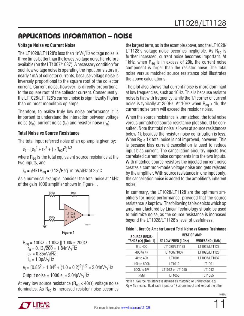
APPLICATIONS INFORMATION – NOISEVoltage Noise vs Current Noise
The LT1028/LT1128’s less than 1nV/√Hz voltage noise is three times better than the lowest voltage noise heretofore available (on the LT1007/1037). A necessary condition for such low voltage noise is operating the input transistors at nearly 1mA of collector currents, because voltage noise is inversely proportional to the square root of the collector current. Current noise, however, is directly proportional to the square root of the collector current. Consequently, the LT1028/LT1128’s current noise is significantly higher than on most monolithic op amps.
Therefore, to realize truly low noise performance it is important to understand the interaction between voltage noise (en), current noise (In) and resistor noise (rn).
Total Noise vs Source Resistance
The total input referred noise of an op amp is given by:
et = [en2 + rn
2 + (InReq)2]1/2
where Req is the total equivalent source resistance at the two inputs, and
rn = √4kTReq = 0.13√Req in nV/√Hz at 25°C
As a numerical example, consider the total noise at 1kHz of the gain 1000 amplifier shown in Figure 1.
the largest term, as in the example above, and the LT1028/LT1128’s voltage noise becomes negligible. As Req is further increased, current noise becomes important. At 1kHz, when Req is in excess of 20k, the current noise component is larger than the resistor noise. The total noise versus matched source resistance plot illustrates the above calculations.
The plot also shows that current noise is more dominant at low frequencies, such as 10Hz. This is because resistor noise is flat with frequency, while the 1/f corner of current noise is typically at 250Hz. At 10Hz when Req > 1k, the current noise term will exceed the resistor noise.
When the source resistance is unmatched, the total noise versus unmatched source resistance plot should be con-sulted. Note that total noise is lower at source resistances below 1k because the resistor noise contribution is less. When RS > 1k total noise is not improved, however. This is because bias current cancellation is used to reduce input bias current. The cancellation circuitry injects two correlated current noise components into the two inputs. With matched source resistors the injected current noise creates a common-mode voltage noise and gets rejected by the amplifier. With source resistance in one input only, the cancellation noise is added to the amplifier’s inherent noise.
In summary, the LT1028/LT1128 are the optimum am-plifiers for noise performance, provided that the source resistance is kept low. The following table depicts which op amp manufactured by Linear Technology should be used to minimize noise, as the source resistance is increased beyond the LT1028/LT1128’s level of usefulness.
Table 1. Best Op Amp for Lowest Total Noise vs Source Resistance
SOURCE RESIS- TANCE (Ω) (Note 1)
BEST OP AMP
AT LOW FREQ (10Hz) WIDEBAND (1kHz)
0 to 400 LT1028/LT1128 LT1028/LT1128
400 to 4k LT1007/1037 LT1028/LT1128
4k to 40k LT1001 LT1007/LT1037
40k to 500k LT1012 LT1001
500k to 5M LT1012 or LT1055 LT1012
>5M LT1055 LT1055
Note 1: Source resistance is defined as matched or unmatched, e.g., RS = 1k means: 1k at each input, or 1k at one input and zero at the other.
Req = 100Ω + 100Ω || 100k ≈ 200Ω rn = 0.13√200 = 1.84nV√Hz en = 0.85nV√Hz In = 1.0pA/√Hz
et = [0.852 + 1.842 + (1.0 × 0.2)2]1/2 = 2.04nV/√Hz
Output noise = 1000 et = 2.04µV/√Hz
At very low source resistance (Req < 40Ω) voltage noise dominates. As Req is increased resistor noise becomes
–
+
100Ω 100k
100ΩLT1028LT1128
1028 F01
Figure 1

LT1028/LT1128
121028fd
For more information www.linear.com/LT1028
APPLICATIONS INFORMATION – NOISENoise Testing – Voltage Noise
The LT1028/LT1128’s RMS voltage noise density can be accurately measured using the Quan Tech Noise Analyzer, Model 5173 or an equivalent noise tester. Care should be taken, however, to subtract the noise of the source resistor used. Prefabricated test cards for the Model 5173 set the device under test in a closed-loop gain of 31 with a 60Ω source resistor and a 1.8k feedback resistor. The noise of this resistor combination is 0.13√58 = 1.0nV/√Hz. An LT1028/LT1128 with 0.85nV/√Hz noise will read (0.852 + 1.02)1/2 = 1.31nV/√Hz. For better resolution, the resistors should be replaced with a 10Ω source and 300Ω feedback resistor. Even a 10Ω resistor will show an apparent noise which is 8% to 10% too high.
The 0.1Hz to 10Hz peak-to-peak noise of the LT1028/LT1128 is measured in the test circuit shown. The fre-quency response of this noise tester indicates that the 0.1Hz corner is defined by only one zero. The test time to measure 0.1Hz to 10Hz noise should not exceed 10 seconds, as this time limit acts as an additional zero to eliminate noise contributions from the frequency band below 0.1Hz.
Measuring the typical 35nV peak-to-peak noise per-formance of the LT1028/LT1128 requires special test precautions:
(a) The device should be warmed up for at least five minutes. As the op amp warms up, its offset voltage changes typically 10µV due to its chip temperature increasing 30°C to 40°C from the moment the power supplies are turned on. In the 10 second measurement interval these temperature-induced effects can easily exceed tens of nanovolts.
(b) For similar reasons, the device must be well shielded from air current to eliminate the possibility of ther-moelectric effects in excess of a few nanovolts, which would invalidate the measurements.
(c) Sudden motion in the vicinity of the device can also feedthrough to increase the observed noise.
A noise-voltage density test is recommended when measur-ing noise on a large number of units. A 10Hz noise-voltage density measurement will correlate well with a 0.1Hz to 10Hz peak-to-peak noise reading since both results are determined by the white noise and the location of the 1/f corner frequency.
Figure 2. 0.1Hz to 10Hz Noise Test Circuit Figure 3. 0.1Hz to 10Hz Peak-to-Peak Noise Tester Frequency Response
–
+
VOLTAGE GAIN = 50,000
* DEVICE UNDER TEST
NOTE ALL CAPACITOR VALUES ARE FOR NONPOLARIZED CAPACITORS ONLY
100k
10Ω
–
+2k
4.7µF
0.1µF
100k
24.3k
22µF
2.2µF
4.3k
110k
SCOPE× 1RIN = 1M
0.1µF
*
1028 F02
LT1001
FREQUENCY (Hz)
40
GAIN
(dB)
60
70
90
100
0.01 1.0 10 100
1028 F03
300.1
50
80
LT1028/LT1128
131028fd
For more information www.linear.com/LT1028
APPLICATIONS INFORMATION – NOISENoise Testing – Current Noise
Current noise density (In) is defined by the following for-mula, and can be measured in the circuit shown in Figure 4.
ln =
eno2 − 31• 18.4nV/ Hz( )2
20k • 31
1/2
If the Quan Tech Model 5173 is used, the noise reading is input-referred, therefore the result should not be divided by 31; the resistor noise should not be multiplied by 31.
100% Noise Testing
The 1kHz voltage and current noise is 100% tested on the LT1028/LT1128 as part of automated testing; the approximate frequency response of the filters is shown. The limits on the automated testing are established by extensive correlation tests on units measured with the Quan Tech Model 5173.
10Hz voltage noise density is sample tested on every lot. Devices 100% tested at 10Hz are available on request for an additional charge.
10Hz current noise is not tested on every lot but it can be inferred from 100% testing at 1kHz. A look at the current noise spectrum plot will substantiate this statement. The only way 10Hz current noise can exceed the guaranteed limits is if its 1/f corner is higher than 800Hz and/or its white noise is high. If that is the case then the 1kHz test will fail.
Figure 5. Automated Tester Noise Filter
–
+eno
1.8k
60Ω LT1028LT1128
10k
10k
1028 F04
FREQUENCY (Hz)
100–50
NOIS
E FI
LTER
LOS
S (d
B)
–10
0
10
1k 10k 100k
1028 F05
–20
–40
–30
CURRENTNOISE
VOLTAGENOISE
Figure 4

LT1028/LT1128
141028fd
For more information www.linear.com/LT1028
Figure 7. Test Circuit for Offset Voltageand Offset Voltage Drift with Temperature
–
+
RF
1028 F08
OUTPUT 6V/µs
–
+
–15V
10k*
200Ω* LT1028LT1128
1028 F07
10k*
VO = 100VOS* RESISTORS MUST HAVE LOW THERMOELECTRIC POTENTIAL
VO6
72
43
15V
APPLICATIONS INFORMATIONGeneral
The LT1028/LT1128 series devices may be inserted directly into OP-07, OP-27, OP-37, LT1007 and LT1037 sockets with or without removal of external nulling components. In addition, the LT1028/LT1128 may be fitted to 5534 sockets with the removal of external compensation components.
Offset Voltage Adjustment
The input offset voltage of the LT1028/LT1128 and its drift with temperature, are permanently trimmed at wafer test-ing to a low level. However, if further adjustment of VOS is necessary, the use of a 1k nulling potentiometer will not degrade drift with temperature. Trimming to a value other than zero creates a drift of (VOS/300)µV/°C, e.g., if VOS is adjusted to 300µV, the change in drift will be 1µV/°C.
The adjustment range with a 1k pot is approximately ±1.1mV.
Unity-Gain Buffer Applications (LT1128 Only)
When RF ≤ 100Ω and the input is driven with a fast, large-signal pulse (>1V), the output waveform will look as shown in the pulsed operation diagram (Figure 8).
–
+
6
1k
INPUT LT1028LT1128
1028 F06
78
12
34
OUTPUT
–15V
15V
Figure 6
Figure 8
Offset Voltage and Drift
Thermocouple effects, caused by temperature gradients across dissimilar metals at the contacts to the input termi-nals, can exceed the inherent drift of the amplifier unless proper care is exercised. Air currents should be minimized, package leads should be short, the two input leads should be close together and maintained at the same temperature.
The circuit shown in Figure 7 to measure offset voltage is also used as the burn-in configuration for the LT1028/LT1128.
During the fast feedthrough-like portion of the output, the input protection diodes effectively short the output to the input and a current, limited only by the output short-circuit protection, will be drawn by the signal generator. With RF ≥ 500Ω, the output is capable of handling the current requirements (IL ≤ 20mA at 10V) and the amplifier stays in its active mode and a smooth transition will occur.
As with all operational amplifiers when RF > 2k, a pole will be created with RF and the amplifier’s input capacitance, creating additional phase shift and reducing the phase margin. A small capacitor (20pF to 50pF) in parallel with RF will eliminate this problem.

LT1028/LT1128
151028fd
For more information www.linear.com/LT1028
APPLICATIONS INFORMATIONFrequency Response
The LT1028’s Gain, Phase vs Frequency plot indicates that the device is stable in closed-loop gains greater than +2 or –1 because phase margin is about 50° at an open-loop gain of 6dB. In the voltage follower configuration phase margin seems inadequate. This is indeed true when the output is shorted to the inverting input and the noninverting input is driven from a 50Ω source impedance. However, when feedback is through a parallel R-C network (provided CF < 68pF), the LT1028 will be stable because of interaction between the input resistance and capacitance and the feedback network. Larger source resistance at the non-inverting input has a similar effect. The following voltage follower configurations are stable:
Another configuration which requires unity-gain stability is shown below. When CF is large enough to effectively short the output to the input at 15MHz, oscillations can occur. The insertion of RS2 ≥ 500Ω will prevent the LT1028 from oscillating. When RS1 ≥ 500Ω, the additional noise contribution due to the presence of RS2 will be minimal. When RS1 ≤ 100Ω, RS2 is not necessary, because RS1 represents a heavy load on the output through the CF short. When 100Ω < RS1 < 500Ω, RS2 should match RS1. For example, RS1 = RS2 = 300Ω will be stable. The noise increase due to RS2 is 40%.
If CF is only used to cut noise bandwidth, a similar effect can be achieved using the over-compensation terminal.
The Gain, Phase plot also shows that phase margin is about 45° at gain of 10 (20dB). The following configuration has a high (≈70%) overshoot without the 10pF capacitor because of additional phase shift caused by the feedback resistor – input capacitance pole. The presence of the 10pF capacitor cancels this pole and reduces overshoot to 5%.
1028 F09
–
+
33pF
2k
LT1028
50Ω
–
+LT1028
50Ω
500Ω
1028 F10
C1
R1
RS1
RS2LT1028
–
+
1028 F11
10pF
10k
50Ω
1.1k–
+LT1028
Figure 9
Over-Compensation
The LT1028/LT1128 are equipped with a frequency over-compensation terminal (Pin 5). A capacitor connected between Pin 5 and the output will reduce noise bandwidth. Details are shown on the Slew Rate, Gain-Bandwidth Prod-uct vs Over-Compensation Capacitor plot. An additional benefit is increased capacitive load handling capability.
Figure 10
Figure 11

LT1028/LT1128
161028fd
For more information www.linear.com/LT1028
Low Noise Voltage Regulator
1028 TA04
10µF
2k
20V OUTPUT
–
+LT1028
121ΩPROVIDES PRE-REGAND CURRENTLIMITING
10µF+
28V
2.32k
2k
330Ω
1000pF
1k
28V
LT317A
OUT
ADJIN
LT1021-10
2N6387
TYPICAL APPLICATIONS
Strain Gauge Signal Conditioner with Bridge Excitation
1028 TA03
1µF
REFERENCEOUTPUT
–
+LT1128
30.1k*
49.9Ω*
15V
330Ω
10kZEROTRIM
5.0V
301k*
LT1021-5
0V TO 10VOUTPUT
3
2
7
6
4
350ΩBRIDGE
–15V
15V
15V
LT1028
–
+
3
2
7
6
4
–15V
LT1028
–
+
3
2
7
6
4
–15V
5kGAINTRIM
330Ω
*RN60C FILM RESISTORS
THE LT1028’s NOISE CONTRIBUTION IS NEGLIGIBLECOMPARED TO THE BRIDGE NOISE.

LT1028/LT1128
171028fd
For more information www.linear.com/LT1028
TYPICAL APPLICATIONS
Paralleling Amplifiers to Reduce Voltage Noise
1028 TA05
–
+1.5kA1
LT1028
470Ω
OUTPUT
–
+
7.5Ω
4.7k
–
+1.5k
470Ω7.5Ω
–
+1.5k
470Ω7.5Ω
A2LT1028
AnLT1028
LT1028
OUTPUT NOISEn • 200
2µV√5
1. ASSUME VOLTAGE NOISE OF LT1028 AND 7.5Ω SOURCE RESISTOR = 0.9nV/√Hz.2. GAIN WITH n LT1028s IN PARALLEL = n • 200.3. OUTPUT NOISE = √n • 200 • 0.9nV/√Hz.
4. INPUT REFERRED NOISE = = nV/√Hz.
5. NOISE CURRENT AT INPUT INCREASES √n TIMES.
6. IF n = 5, GAIN = 1000, BANDWIDTH = 1MHz, RMS NOISE, DC TO 1MHz = = 0.9µV.
0.9√n

LT1028/LT1128
181028fd
For more information www.linear.com/LT1028
Tape Head Amplifier
Phono Preamplifier
TYPICAL APPLICATIONS
1028 TA06
0.1µF
10Ω
–15V
10k
–
+LT1028 OUTPUT
787Ω
0.33µF
100pF
47k
MAG PHONOINPUT
4
6
7
15V
2
3
ALL RESISTORS METAL FILM
1028 TA07
0.1µF
10Ω–
+LT1028 OUTPUT
499Ω
TAPE HEADINPUT
6
31.6k
2
3
ALL RESISTORS METAL FILM

LT1028/LT1128
191028fd
For more information www.linear.com/LT1028
Low Noise, Wide Bandwidth Instrumentation Amplifier
Gyro Pick-Off Amplifier
TYPICAL APPLICATIONS
1028 TA08
10Ω
–
+LT1028
OUTPUT820Ω
+INPUT
68pF
10k
50Ω
68pF820Ω–
+LT1028
–INPUT
–
+LT1028
300Ω
300Ω 10k
GAIN = 1000, BANDWIDTH = 1MHzINPUT REFERRED NOISE = 1.5nV/√Hz AT 1kHzWIDEBAND NOISE –DC to 1MHz = 3µVRMSIF BW LIMITED TO DC TO 100kHz = 0.55µVRMS
1028 TA09
100Ω
OUTPUT TO SYNCDEMODULATOR
1k–
+LT1028
SINEDRIVE
•
GYRO TYPICAL–NORTHROP CORP.
GR-F5AH7-5B

LT1028/LT1128
201028fd
For more information www.linear.com/LT1028
1028 TA10
–
+LT1028
C20.047
R2
R1C10.047
2k
20Ω
20Ω 2k
10pF
5.6k
15µF+
22k
10k
–
+
LT1055
1VRMS OUTPUT1.5kHz TO 15kHz
WHERE R1C1 = R2C2
f = 12πRC( )
MOUNT 1N4148sIN CLOSE PROXIMITY
TRIM FORLOWEST
DISTORTION
100k10k
20k
2N4338
560Ω
2.4k4.7k
LT1004-1.2V
15V
<0.0018% DISTORTION AND NOISE.MEASUREMENT LIMITED BY RESOLUTION OFHP339A DISTORTION ANALYZER
1028 TA11
–
+LT1052
10Ω
0.1
30k
10k
15V
7
6
42
3
8
1
–15V
0.10.01
15V
68Ω
–
+LT1028
130Ω
1
7
8
4
–15V
INPUT
OUTPUT
1N758
1N758
100k
2
3
TYPICAL APPLICATIONSSuper Low Distortion Variable Sine Wave Oscillator
Chopper-Stabilized Amplifier

LT1028/LT1128
211028fd
For more information www.linear.com/LT1028
SCHEMATIC DIAGRAM
1.5µA
1NULL
R5130Ω
R6130Ω
R13k
R23k
3
8NULL
Q4
C1257pF
900µA 900µA
Q6Q5
Q9Q8Q7
Q24.5µA
4.5µA
1.5µA
Q13Q14
Q14.5µA
NON-INVERTING
INPUT
0
1.8mA
Q3BIAS
2
INVERTINGINPUT
4V–
R780Ω
Q11
Q10
Q12
300µA
Q15
Q21
5 OVER-COMP
Q23
600µA
R12240Ω
C435pF
Q22R11
100Ω
C3250pF
Q19
Q18
Q16
Q17R11400Ω
R10400Ω
1.1mA 2.3mA 400µA
V+
7
R10500Ω
C2
Q26
Q25Q24
6OUTPUT
Q27
1028 TA12
4.5µA
31
31
Q20
R8480Ω
500µA
C2 = 50pF for LT1028C2 = 275pF for LT1128
LT1028/LT1128
221028fd
For more information www.linear.com/LT1028
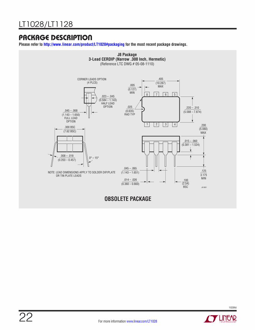
PACKAGE DESCRIPTIONPlease refer to http://www.linear.com/product/LT1028#packaging for the most recent package drawings.
OBSOLETE PACKAGE
J8 0801
.014 – .026(0.360 – 0.660)
.200(5.080)
MAX
.015 – .060(0.381 – 1.524)
.1253.175MIN
.100(2.54)BSC
.300 BSC(7.62 BSC)
.008 – .018(0.203 – 0.457)
0° – 15°
.005(0.127)
MIN
.405(10.287)
MAX
.220 – .310(5.588 – 7.874)
1 2 3 4
8 7 6 5
.025(0.635)
RAD TYP.045 – .068
(1.143 – 1.650)FULL LEAD
OPTION
.023 – .045(0.584 – 1.143)
HALF LEADOPTION
CORNER LEADS OPTION (4 PLCS)
.045 – .065(1.143 – 1.651)NOTE: LEAD DIMENSIONS APPLY TO SOLDER DIP/PLATE
OR TIN PLATE LEADS
J8 Package3-Lead CERDIP (Narrow .300 Inch, Hermetic)
(Reference LTC DWG # 05-08-1110)

LT1028/LT1128
231028fd
For more information www.linear.com/LT1028
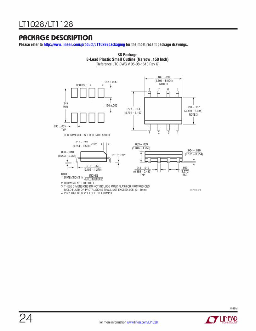
PACKAGE DESCRIPTIONPlease refer to http://www.linear.com/product/LT1028#packaging for the most recent package drawings.
N8 REV I 0711
.065(1.651)
TYP
.045 – .065(1.143 – 1.651)
.130 ±.005(3.302 ±0.127)
.020(0.508)
MIN.018 ±.003(0.457 ±0.076)
.120(3.048)
MIN
.008 – .015(0.203 – 0.381)
.300 – .325(7.620 – 8.255)
.325+.035–.015+0.889–0.3818.255( )
1 2 3 4
8 7 6 5
.255 ±.015*(6.477 ±0.381)
.400*(10.160)
MAX
NOTE:1. DIMENSIONS ARE
INCHESMILLIMETERS
*THESE DIMENSIONS DO NOT INCLUDE MOLD FLASH OR PROTRUSIONS. MOLD FLASH OR PROTRUSIONS SHALL NOT EXCEED .010 INCH (0.254mm)
.100(2.54)BSC
N Package8-Lead PDIP (Narrow .300 Inch)
(Reference LTC DWG # 05-08-1510 Rev I)
LT1028/LT1128
241028fd
For more information www.linear.com/LT1028
PACKAGE DESCRIPTIONPlease refer to http://www.linear.com/product/LT1028#packaging for the most recent package drawings.
.016 – .050(0.406 – 1.270)
.010 – .020(0.254 – 0.508)
× 45°
0°– 8° TYP.008 – .010
(0.203 – 0.254)
SO8 REV G 0212
.053 – .069(1.346 – 1.752)
.014 – .019(0.355 – 0.483)
TYP
.004 – .010(0.101 – 0.254)
.050(1.270)
BSC
1 2 3 4
.150 – .157(3.810 – 3.988)
NOTE 3
8 7 6 5
.189 – .197(4.801 – 5.004)
NOTE 3
.228 – .244(5.791 – 6.197)
.245MIN .160 ±.005
RECOMMENDED SOLDER PAD LAYOUT
.045 ±.005 .050 BSC
.030 ±.005 TYP
INCHES(MILLIMETERS)
NOTE:1. DIMENSIONS IN
2. DRAWING NOT TO SCALE3. THESE DIMENSIONS DO NOT INCLUDE MOLD FLASH OR PROTRUSIONS. MOLD FLASH OR PROTRUSIONS SHALL NOT EXCEED .006" (0.15mm)4. PIN 1 CAN BE BEVEL EDGE OR A DIMPLE
S8 Package8-Lead Plastic Small Outline (Narrow .150 Inch)
(Reference LTC DWG # 05-08-1610 Rev G)
LT1028/LT1128
251028fd
For more information www.linear.com/LT1028
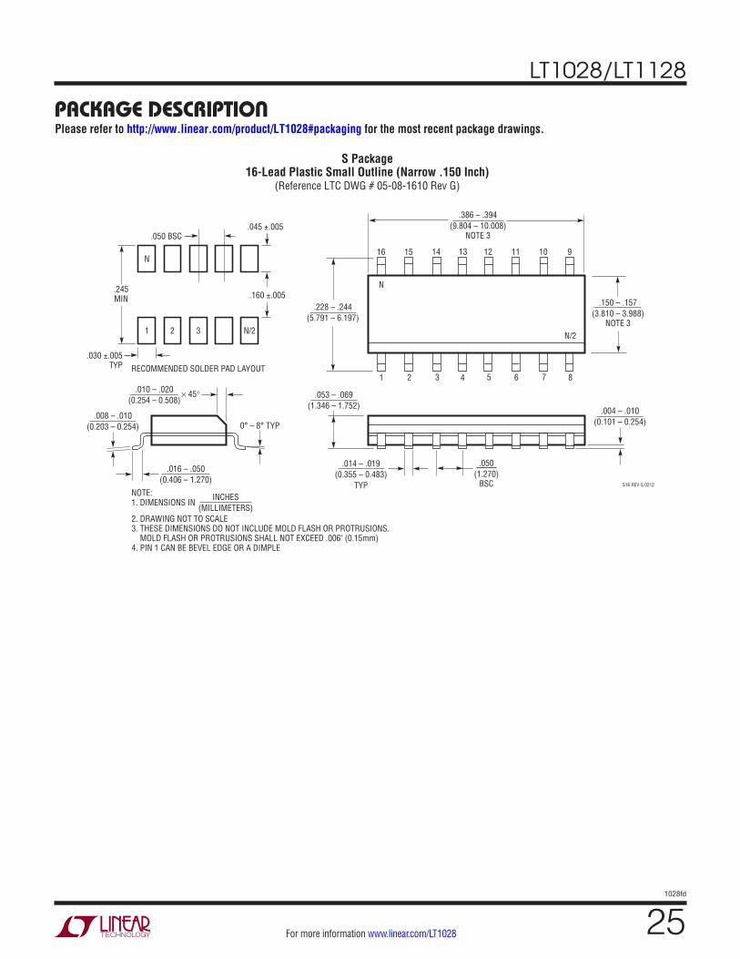
PACKAGE DESCRIPTIONPlease refer to http://www.linear.com/product/LT1028#packaging for the most recent package drawings.
.016 – .050(0.406 – 1.270)
.010 – .020(0.254 – 0.508)
× 45°
0° – 8° TYP.008 – .010
(0.203 – 0.254)
1
N
2 3 4 5 6 7 8
N/2
.150 – .157(3.810 – 3.988)
NOTE 3
16 15 14 13
.386 – .394(9.804 – 10.008)
NOTE 3
.228 – .244(5.791 – 6.197)
12 11 10 9
S16 REV G 0212
.053 – .069(1.346 – 1.752)
.014 – .019(0.355 – 0.483)
TYP
.004 – .010(0.101 – 0.254)
.050(1.270)
BSC
.245MIN
N
1 2 3 N/2
.160 ±.005
RECOMMENDED SOLDER PAD LAYOUT
.045 ±.005 .050 BSC
.030 ±.005 TYP
INCHES(MILLIMETERS)
NOTE:1. DIMENSIONS IN
2. DRAWING NOT TO SCALE3. THESE DIMENSIONS DO NOT INCLUDE MOLD FLASH OR PROTRUSIONS. MOLD FLASH OR PROTRUSIONS SHALL NOT EXCEED .006" (0.15mm)4. PIN 1 CAN BE BEVEL EDGE OR A DIMPLE
S Package16-Lead Plastic Small Outline (Narrow .150 Inch)
(Reference LTC DWG # 05-08-1610 Rev G)

LT1028/LT1128
261028fd
For more information www.linear.com/LT1028
PACKAGE DESCRIPTION
OBSOLETE PACKAGE
Please refer to http://www.linear.com/product/LT1028#packaging for the most recent package drawings.
.050(1.270)
MAX
.016 – .021**(0.406 – 0.533)
.010 – .045*(0.254 – 1.143)
SEATINGPLANE
.040(1.016)
MAX .165 – .185(4.191 – 4.699)
GAUGEPLANE
REFERENCEPLANE
.500 – .750(12.700 – 19.050)
.305 – .335(7.747 – 8.509)
.335 – .370(8.509 – 9.398)
DIA
.230(5.842)
TYP
.027 – .045(0.686 – 1.143)
.028 – .034(0.711 – 0.864)
.110 – .160(2.794 – 4.064)
INSULATINGSTANDOFF
45°
H8 (TO-5) 0.230 PCD 0204
LEAD DIAMETER IS UNCONTROLLED BETWEEN THE REFERENCE PLANE AND THE SEATING PLANE
FOR SOLDER DIP LEAD FINISH, LEAD DIAMETER IS.016 – .024
(0.406 – 0.610)
*
**
PIN 1
H Package8-Lead TO-5 Metal Can (.230 Inch PCD)
(Reference LTC DWG # 05-08-1321)

LT1028/LT1128
271028fd
For more information www.linear.com/LT1028
Information furnished by Linear Technology Corporation is believed to be accurate and reliable. However, no responsibility is assumed for its use. Linear Technology Corporation makes no representa-tion that the interconnection of its circuits as described herein will not infringe on existing patent rights.
REVISION HISTORYREV DATE DESCRIPTION PAGE NUMBER
B 10/12 Replaced the Typical Application. 1
C 10/14 Corrected diagram to show N8 package is not obsolete.Changed TJMAX to 150°C for S8 and SW packages.Corrected right-hand Electrical Characteristics column to reflect non-A-grade specs.Corrected LM301A and LT1012 input polarity.
223
28
D 10/15 Corrected component values in Low Noise Voltage Regulator circuit. 16
(Revision history begins at Rev B)
LT1028/LT1128
281028fd
For more information www.linear.com/LT1028 LINEAR TECHNOLOGY CORPORATION 1992
LT 1015 REV D • PRINTED IN USALinear Technology Corporation1630 McCarthy Blvd., Milpitas, CA 95035-7417(408) 432-1900 FAX: (408) 434-0507 www.linear.com/LT1028
RELATED PARTS
TYPICAL APPLICATION
PART NUMBER DESCRIPTION COMMENTS
LT1806/LT1807 325MHz, 3.5nV/√Hz Single and Dual Op Amps Slew Rate = 140V/µs, Low Distortion at 5MHz: –80dBc
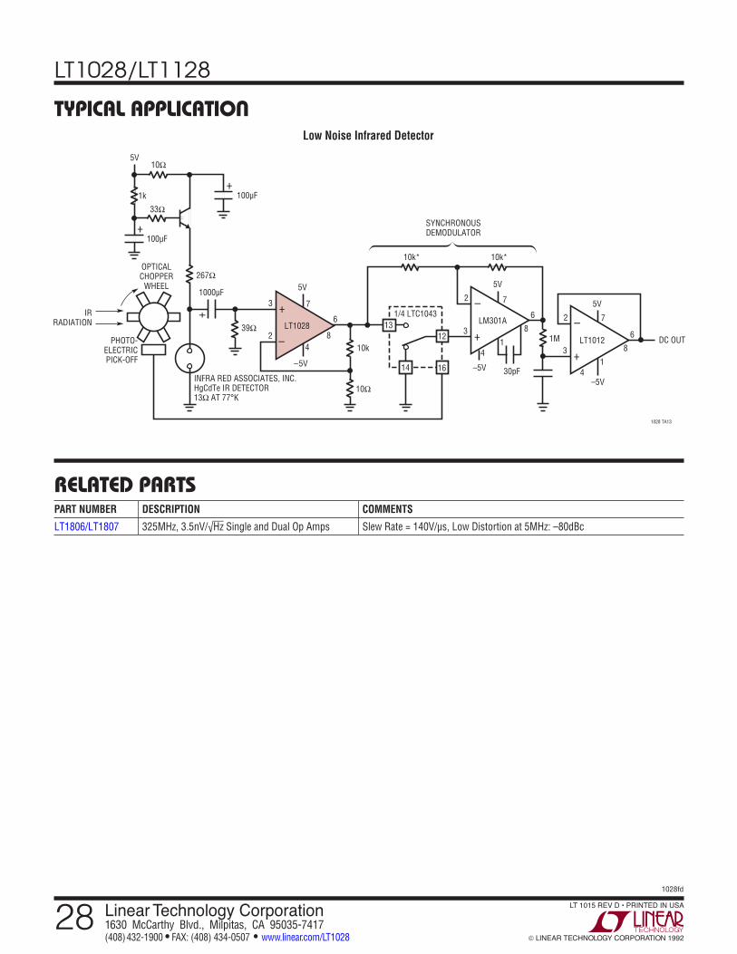
Low Noise Infrared Detector
1028 TA13
10Ω
1M
1k
10k
5V
–
+LT1028
7
6
42
3
8
–5V
1000µF
DC OUT
5V
39Ω
33Ω+
267Ω
10Ω
+
+
OPTICALCHOPPER
WHEEL
IRRADIATION
PHOTO-ELECTRICPICK-OFF
INFRA RED ASSOCIATES, INC.HgCdTe IR DETECTOR13Ω AT 77°K
1/4 LTC1043
30pF
100µF
100µF
13
14 16
10k* 10k*
SYNCHRONOUSDEMODULATOR
+
–LT1012
7
4
2
3
–5V
6
5V
1
812 +
–LM301A
7
4
2
3
–5V
6
5V
1
8