lt1818/lt1819 - 400mhz, 2500v/ms, 9ma single/dual ... · pdf file9ma supply current per...
TRANSCRIPT

1
LT1818/LT1819
18189f
400MHz, 2500V/µs, 9mASingle/Dual Operational Amplifiers
400MHz Gain Bandwidth Product 2500V/µs Slew Rate –85dBc Distortion at 5MHz 9mA Supply Current Per Amplifier Space Saving SOT-23 and MS8 Packages 6nV/√Hz Input Noise Voltage Unity-Gain Stable 1.5mV Maximum Input Offset Voltage 8µA Maximum Input Bias Current 800nA Maximum Input Offset Current 40mA Minimum Output Current, VOUT = ±3V ±3.5V Minimum Input CMR, VS = ±5V Specified at ±5V, Single 5V Supplies Operating Temperature Range: –40°C to 85°C
Wideband Amplifiers Buffers Active Filters Video and RF Amplification Communication Receivers Cable Drivers Data Acquisition Systems
, LTC and LT are registered trademarks of Linear Technology Corporation.
The LT®1818/LT1819 are single/dual wide bandwidth,high slew rate, low noise and distortion operational ampli-fiers with excellent DC performance. The LT1818/LT1819have been designed for wider bandwidth and slew rate,much lower input offset voltage and lower noise anddistortion than devices with comparable supply current.The circuit topology is a voltage feedback amplifier withthe excellent slewing characteristics of a current feedbackamplifier.
The output drives a 100Ω load to ±3.8V with ±5V supplies.On a single 5V supply, the output swings from 1V to 4Vwith a 100Ω load connected to 2.5V. The amplifier is unity-gain stable with a 20pF capacitive load without the need fora series resistor. Harmonic distortion is –85dBc up to5MHz for a 2VP-P output at a gain of 2.
The LT1818/LT1819 are manufactured on LinearTechnology’s advanced low voltage complementary bipo-lar process. The LT1818 (single op amp) is available inSOT-23 and SO-8 packages; the LT1819 (dual op amp) isavailable in MSOP-8 and SO-8 packages.
–
+LT1818
2.5VDC±1VAC
18189 TA01
18pF2.5V
51.1Ω
5V 5V
AIN+
LTC174414 BITS50Msps
(SET FOR 2VP-PFULL SCALE)
AIN–
Single Supply Unity-Gain ADC Driver for Oversampling Applications
FREQUENCY (Hz)
AMPL
ITUD
E (d
Bc)
0
–10
–20
–30
–40
–50
–60
–70
–80
–90
–100
–1100
18189 TA02
5M 10M 15M 20M 25M
fIN = 5.102539MHzfS = 50MspsVIN = 300mVP-PSFDR = 78dB8192 POINT FFTNO WINDOWINGOR AVERAGING
2 3
FFT of Single Supply ADC Driver
APPLICATIO SU
FEATURES
TYPICAL APPLICATIO
U
DESCRIPTIO
U

2
LT1818/LT1819
18189f
(Note 1)Total Supply Voltage (V+ to V–) ........................... 12.6VDifferential Input Voltage
(Transient Only, Note 2) ..................................... ±6VOutput Short-Circuit Duration (Note 3) ........... IndefiniteOperating Temperature Range (Note 8) .. –40°C to 85°C
ABSOLUTE AXI U RATI GS
W WW U
PACKAGE/ORDER I FOR ATIOU UW
*The temperature grade is identified by a label on the shipping container. Consult LTC Marketing for parts specified with wider operating temperature ranges.
Specified Temperature Range (Note 9) ... –40°C to 85°CMaximum Junction Temperature .......................... 150°CStorage Temperature Range ................. –65°C to 150°CLead Temperature (Soldering, 10 sec).................. 300°C
1234
OUT A–IN A+IN A
V–
8765
V+
OUT B–IN B+IN B
TOP VIEW
MS8 PACKAGE8-LEAD PLASTIC MSOP
BA
TOP VIEW
S5 PACKAGE5-LEAD PLASTIC SOT-23
1
2
3
OUT 1
V–
+IN
5
4
V+
–IN+ –
LTF7
S5 PART*MARKING
ORDER PARTNUMBER
LT1818CS5LT1818IS5
LTE7LTE5
MS8 PARTMARKING
ORDER PARTNUMBER
TJMAX = 150°C, θJA = 250°C/W (NOTE 10)TJMAX = 150°C, θJA = 250°C/W (NOTE 10)
LT1819CMS8LT1819IMS8
TJMAX = 150°C, θJA = 150°C/W (NOTE 10)
1
2
3
4
8
7
6
5
TOP VIEW
–+
NC
V+
OUT
NC
NC
–IN
+IN
V–
S8 PACKAGE8-LEAD PLASTIC SO
LT1818CS8LT1818IS8
ORDER PARTNUMBER
18181818I
S8 PARTMARKING
TJMAX = 150°C, θJA = 150°C/W (NOTE 10)
ELECTRICAL CHARACTERISTICS
SYMBOL PARAMETER CONDITIONS MIN TYP MAX UNITS
VOS Input Offset Voltage (Note 4) 0.2 1.5 mV TA = 0°C to 70°C 2.0 mV TA = –40°C to 85°C 3.0 mV
∆VOS/∆T Input Offset Voltage Drift TA = 0°C to 70°C (Note 7) 10 15 µV/°CTA = –40°C to 85°C (Note 7) 10 30 µV/°C
IOS Input Offset Current 60 800 nATA = 0°C to 70°C 1000 nATA = –40°C to 85°C 1200 nA
IB Input Bias Current –2 ±8 µATA = 0°C to 70°C ±10 µATA = –40°C to 85°C ±12 µA
en Input Noise Voltage Density f = 10kHz 6 nV/√Hz
in Input Noise Current Density f = 10kHz 1.2 pA/√Hz
The denotes the specifications which apply over the full operatingtemperature range, otherwise specifications are at TA = 25°C. (Note 9) VS = ±5V, VCM = 0V, unless otherwise noted.
LT1819CS8LT1819IS8
ORDER PARTNUMBER
18191819I
S8 PARTMARKING
1
2
3
4
8
7
6
5
TOP VIEW
V+
OUT B
–IN B
+IN B
OUT A
–IN A
+IN A
V–
S8 PACKAGE8-LEAD PLASTIC SO
A
B

3
LT1818/LT1819
18189f
SYMBOL PARAMETER CONDITIONS MIN TYP MAX UNITSRIN Input Resistance VCM = V– + 1.5V to V+ – 1.5V 1.5 5 MΩ
Differential 750 kΩCIN Input Capacitance 1.5 pFVCM Input Voltage Range Guaranteed by CMRR ±3.5 ±4.2 V
(Positive/Negative) TA = –40°C to 85°C ±3.5 VCMRR Common Mode Rejection Ratio VCM = ±3.5V 75 85 dB
TA = 0°C to 70°C 73 dB TA = –40°C to 85°C 72 dB
Minimum Supply Voltage Guaranteed by PSRR ±1.25 ±2 V TA = –40°C to 85°C ±2 V
PSRR Power Supply Rejection Ratio VS = ±2V to ±5.5V 78 97 dB TA = 0°C to 70°C 76 dB TA = –40°C to 85°C 75 dB
AVOL Large-Signal Voltage Gain VOUT = ±3V, RL = 500Ω 1.5 2.5 V/mV TA = 0°C to 70°C 1.0 V/mV TA = –40°C to 85°C 0.8 V/mVVOUT = ±3V, RL = 100Ω 1.0 6 V/mV TA = 0°C to 70°C 0.7 V/mV TA = –40°C to 85°C 0.6 V/mV
Channel Separation VOUT = ±3V, LT1819 82 100 dB TA = 0°C to 70°C 81 dB TA = –40°C to 85°C 80 dB
VOUT Output Swing(Positive/Negative) RL = 500Ω, 30mV Overdrive ±3.8 ±4.1 V TA = 0°C to 70°C ±3.7 V TA = –40°C to 85°C ±3.6 VRL = 100Ω, 30mV Overdrive ±3.50 ±3.8 V TA = 0°C to 70°C ±3.25 V TA = –40°C to 85°C ±3.15 V
IOUT Output Current VOUT = ±3V, 30mV Overdrive ±40 ±70 mA TA = 0°C to 70°C ±35 mA TA = –40°C to 85°C ±30 mA
ISC Output Short-Circuit Current VOUT = 0V, 1V Overdrive (Note 3) ±100 ±200 mA TA = 0°C to 70°C ±90 mA TA = –40°C to 85°C ±70 mA
SR Slew Rate AV = 1 2500 V/µsAV = –1 (Note 5) 900 1800 V/µs TA = 0°C to 70°C 750 V/µs TA = –40°C to 85°C 600 V/µs
FPBW Full Power Bandwidth 6VP-P (Note 6) 95 MHzGBW Gain Bandwidth Product f = 4MHz, RL = 500Ω 270 400 MHz
TA = 0°C to 70°C 260 MHz TA = –40°C to 85°C 250 MHz
tr, tf Rise Time, Fall Time AV = 1, 10% to 90%, 0.1V Step 0.6 nstPD Propagation Delay AV = 1, 50% to 50%, 0.1V Step 1.0 nsOS Overshoot AV = 1, 0.1V, RL = 100Ω 20 %tS Settling Time AV = –1, 0.1%, 5V 10 nsHD Harmonic Distortion HD2, AV = 2, f = 5MHz, VOUT = 2VP-P, RL = 500Ω –85 dBc
HD3, AV = 2, f = 5MHz, VOUT = 2VP-P, RL = 500Ω –89 dBcdG Differential Gain AV = 2, RL = 150Ω 0.07 %dP Differential Phase AV = 2, RL = 150Ω 0.02 DEGIS Supply Current Per Amplifier 9 10 mA
TA = 0°C to 70°C 13 mA TA = –40°C to 85°C 14 mA
ELECTRICAL CHARACTERISTICS The denotes the specifications which apply over the full operatingtemperature range, otherwise specifications are at TA = 25°C. (Note 9) VS = ±5V, VCM = 0V, unless otherwise noted.

4
LT1818/LT1819
18189f
ELECTRICAL CHARACTERISTICS The denotes the specifications which apply over the full operatingtemperature range, otherwise specifications are at TA = 25°C (Note 9). VS = 5V, 0V; VCM = 2.5V, RL to 2.5V unless otherwise noted.
SYMBOL PARAMETER CONDITIONS MIN TYP MAX UNITS
VOS Input Offset Voltage (Note 4) 0.4 2.0 mV TA = 0°C to 70°C 2.5 mV TA = –40°C to 85°C 3.5 mV
∆VOS/∆T Input Offset Voltage Drift (Note 7) TA = 0°C to 70°C 10 15 µV/°C TA = –40°C to 85°C 10 30 µV/°C
IOS Input Offset Current 60 800 nATA = 0°C to 70°C 1000 nATA = –40°C to 85°C 1200 nA
IB Input Bias Current –2.4 ±8 µATA = 0°C to 70°C ±10 µATA = –40°C to 85°C ±12 µA
en Input Noise Voltage Density f = 10kHz 6 nV/√Hz
in Input Noise Current Density f = 10kHz 1.4 pA/√Hz
RIN Input Resistance VCM = V– + 1.5V to V+ – 1.5V 1.5 5 MΩDifferential 750 kΩ
CIN Input Capacitance 1.5 pF
VCM Input Voltage Range (Positive) Guaranteed by CMRR 3.5 4.2 V TA = –40°C to 85°C 3.5 V
Input Voltage Range (Negative) Guaranteed by CMRR 0.8 1.5 V TA = –40°C to 85°C 1.5 V
CMRR Common Mode Rejection Ratio VCM = 1.5V to 3.5V 73 82 dB TA = 0°C to 70°C 71 dB TA = –40°C to 85°C 70 dB
Minimum Supply Voltage Guaranteed by PSRR ±1.25 ±2 V TA = –40°C to 85°C ±2 V
PSRR Power Supply Rejection Ratio VS = 4V to 11V 78 97 dB TA = 0°C to 70°C 76 dB TA = –40°C to 85°C 75 dB
AVOL Large-Signal Voltage Gain VOUT = 1.5V to 3.5V, RL = 500Ω 1.0 2 V/mV TA = 0°C to 70°C 0.7 V/mV TA = –40°C to 85°C 0.6 V/mV
VOUT = 1.5V to 3.5V, RL = 100Ω 0.7 4 V/mV TA = 0°C to 70°C 0.5 V/mV TA = –40°C to 85°C 0.4 V/mV
Channel Separation VOUT = 1.5V to 3.5V, LT1819 81 100 dB TA = 0°C to 70°C 80 dB TA = –40°C to 85°C 79 dB
VOUT Output Swing(Positive) RL = 500Ω, 30mV Overdrive 3.9 4.2 V TA = 0°C to 70°C 3.8 V TA = –40°C to 85°C 3.7 V
RL = 100Ω, 30mV Overdrive 3.7 4 V TA = 0°C to 70°C 3.6 V TA = –40°C to 85°C 3.5 V
Output Swing(Negative) RL = 500Ω, 30mV Overdrive 0.8 1.1 V TA = 0°C to 70°C 1.2 V TA = –40°C to 85°C 1.3 V
RL = 100Ω, 30mV Overdrive 1 1.3 V TA = 0°C to 70°C 1.4 V TA = –40°C to 85°C 1.5 V

5
LT1818/LT1819
18189f
ELECTRICAL CHARACTERISTICS The denotes the specifications which apply over the full operatingtemperature range, otherwise specifications are at TA = 25°C (Note 9). VS = 5V, 0V; VCM = 2.5V, RL to 2.5V unless otherwise noted.
Note 1: Absolute Maximum Ratings are those values beyond which the lifeof a device may be impaired.Note 2: Differential inputs of ±6V are appropriate for transient operationonly, such as during slewing. Large sustained differential inputs can causeexcessive power dissipation and may damage the part.Note 3: A heat sink may be required to keep the junction temperaturebelow absolute maximum when the output is shorted indefinitely.Note 4: Input offset voltage is pulse tested and is exclusive of warm-updrift.Note 5: With ±5V supplies, slew rate is tested in a closed-loop gain of –1by measuring the rise time of the output from –2V to 2V with an outputstep from –3V to 3V. With single 5V supplies, slew rate is tested in aclosed-loop gain of –1 by measuring the rise time of the output from 1.5Vto 3.5V with an output step from 1V to 4V. Falling edge slew rate is notproduction tested, but is designed, characterized and expected to be within10% of the rising edge slew rate.
Note 6: Full power bandwidth is calculated from the slew rate:FPBW = SR/2πVP
Note 7: This parameter is not 100% tested.Note 8: The LT1818C/LT1818I and LT1819C/LT1819I are guaranteedfunctional over the operating temperature range of – 40°C to 85°C.Note 9: The LT1818C/LT1819C are guaranteed to meet specifiedperformance from 0°C to 70°C and is designed, characterized andexpected to meet the extended temperature limits, but is not tested at–40°C and 85°C. The LT1818I/LT1819I are guaranteed to meet theextended temperature limits.Note 10: Thermal resistance (θJA) varies with the amount of PC boardmetal connected to the package. The specified values are for short tracesconnected to the leads. If desired, the thermal resistance can besignificantly reduced by connecting the V– pin to a large metal area.
SYMBOL PARAMETER CONDITIONS MIN TYP MAX UNITS
IOUT Output Current VOUT = 1.5V or 3.5V, 30mV Overdrive ±30 ±50 mA TA = 0°C to 70°C ±25 mA TA = –40°C to 85°C ±20 mA
ISC Output Short-Circuit Current VOUT = 2.5V, 1V Overdrive (Note 3) ±80 ±140 mA TA = 0°C to 70°C ±70 mA TA = –40°C to 85°C ±50 mA
SR Slew Rate AV = 1 1000 V/µs
AV = –1 (Note 5) 450 800 V/µs TA = 0°C to 70°C 375 V/µs TA = –40°C to 85°C 300 V/µs
FPBW Full Power Bandwidth 2VP-P (Note 6) 125 MHz
GBW Gain Bandwidth Product f = 4MHz, RL = 500Ω 240 360 MHz TA = 0°C to 70°C 230 MHz TA = –40°C to 85°C 220 MHz
tr, tf Rise Time, Fall Time AV = 1, 10% to 90%, 0.1V Step 0.7 ns
tPD Propagation Delay AV = 1, 50% to 50%, 0.1V Step 1.1 ns
OS Overshoot AV = 1, 0.1V, RL = 100Ω 20 %
HD Harmonic Distortion HD2, AV = 2, f = 5MHz, VOUT = 2VP-P, RL = 500Ω –72 dBcHD3, AV = 2, f = 5MHz, VOUT = 2VP-P, RL = 500Ω –74 dBc
dG Differential Gain AV = 2, RL = 150Ω 0.07 %
dP Differential Phase AV = 2, RL = 150Ω 0.07 DEG
IS Supply Current Per Amplifier 8.5 10 mA TA = 0°C to 70°C 13 mA TA = –40°C to 85°C 14 mA

6
LT1818/LT1819
18189f
TYPICAL PERFOR A CE CHARACTERISTICS
UW
Supply Current vs TemperatureInput Common Mode Rangevs Supply Voltage
Input Bias Current vs CommonMode Voltage
Input Noise Spectral Density Open-Loop Gain vs Resistive LoadInput Bias Current vs Temperature
Output Voltage Swingvs Supply Voltage
Output Voltage Swingvs Load CurrentOpen-Loop Gain vs Temperature
TEMPERATURE (°C)–50 –25
0
SUPP
LY C
URRE
NT (m
A)
4
12
10
0 50 75
18189 G01
2
8
6
25 100 125
VS = ±5V
VS = ±2.5V
PER AMPLIFIER
SUPPLY VOLTAGE (± V)0
V –
INPU
T CO
MM
ON M
ODE
RANG
E (V
)
1.0
1.5
2.0
V +
–2.0
–1.5
2 4 5
18189 G02
0.5
–1.0
–0.5
1 3 6 7
TA = 25°C∆VOS < 1mV
INPUT COMMON MODE VOLTAGE (V)–5
INPU
T BI
AS C
URRE
NT (µ
A)
TA = 25°CVS = ±5V
5
18189 G03
–2.5 0 2.5
2
0
–2
–4
–6
–8
TEMPERATURE (°C)–50
–1.2
–0.8
0
25 75
18189 G04
–1.6
–2.0
–25 0 50 100 125
–2.4
–2.8
–0.4
INPU
T BI
AS C
URRE
NT (µ
A)
VS = ±5V
VS = ±2.5V
VCM = 0V
FREQUENCY (Hz)10 100
1
10
in
100
0.1
1
10
1k 10k 100k
18189 G05
TA = 25°CVS = ±5VAV = 101RS = 10k
en
INPU
T VO
LTAG
E NO
ISE
(nV/
√Hz)
INPUT CURRENT NOISE (pA/√Hz)
LOAD RESISTANCE (Ω)100
OPEN
-LOO
P GA
IN (d
B)
80
77
74
71
68
65
621k 10k
18189 G06
TA = 25°C
VS = ±5V
VS = ±2.5V
TEMPERATURE (°C)–50
OPEN
-LOO
P GA
IN (d
B)
80
77
74
71
68
65
6225 75
18189 G07
–25 0 50 100 125
VS = ±5VVO = ±3V
RL = 100Ω
RL = 500Ω
SUPPLY VOLTAGE (± V)0
V –
OUTP
UT V
OLTA
GE S
WIN
G (V
)
1.0
1.5
2.0
V +
–2.0
–1.5
2 4 5
18189 G08
0.5
–1.0
–0.5
1 3 6 7
TA = 25°C∆VOS = 30mV
RL = 100Ω
RL = 100Ω
RL = 500Ω
RL = 500Ω
OUTPUT CURRENT (mA)–120
OUTP
UT V
OLTA
GE S
WIN
G (V
) OUTPUT VOLTAGE SWING (V)
–2
40
18189 G09
–3
–4
–5
5
4
3
2
–80 –40 0 80 120
TA = 25°CVS = ±5V∆VOS = 30mV
SINK
SOURCE

7
LT1818/LT1819
18189f
TYPICAL PERFOR A CE CHARACTERISTICS
UW
Output Current vs Temperature Output Impedance vs FrequencyOutput Short-Circuit Currentvs Temperature
Gain Bandwidth and PhaseMargin vs TemperatureGain and Phase vs Frequency
Gain vs Frequency, AV = 1 Gain vs Frequency, AV = 2
TEMPERATURE (°C)–50
OUTP
UT S
HORT
-CIR
CUIT
CUR
RENT
(mA)
160
200
240
25 75
18189 G10
120
80
–25 0 50 100 125
40
0
SOURCE
SINK
VS = ± 5VVIN = ±1V
TEMPERATURE (˚C)–50
OUTU
PT C
URRE
NT (m
A)
100
125
150
25 75
18189 G11
75
50
–25 0 50 100 125
25
0
∆VOS = 30mVVOUT = ±3V FOR VS = ±5VVOUT = ±1V FOR VS = ±2.5V
SOURCE, VS = ±5V
SINK, VS = ±5V SOURCE, VS = ±2.5V
SINK, VS = ±2.5V
FREQUENCY (Hz)10k 100k
0.01
OUTP
UT IM
PEDA
NCE
(Ω)
0.1
100
1M 10M 100M
18189 G12
1
10 AV = 100
AV = 10
AV = 1
TA = 25°CVS = ± 5V
FREQUENCY (Hz)10k
20GAIN
(dB)
PHASE (DEG)
30
40
50
60
100k 1M 500M100M10M
18189 G13
10
0
–10
–20
70
80
60
80
100
120
140
40
20
0
–20
160
180
TA = 25°CAV = –1RL = 500Ω
GAINPHASE
TEMPERATURE (°C)–50 –25
GAIN
BAN
DWID
TH (M
Hz) PHASE M
ARGIN (DEG)
440
0 50 75
18189 G15
30
50
40
400
360
25 100 125
GBWVS = ±5V
GBWVS = ±2.5V
RL = 500Ω
PHASE MARGINVS = ±2.5V
PHASE MARGINVS = ±5V
FREQUENCY (Hz)1M
GAIN
(dB)
–5
0
10M 100M 500M
18189 G16
–10
5TA = 25°CAV = 1RL = 500Ω VS = ±2.5V
VS = ±5V
FREQUENCY (Hz)1M
GAIN
(dB)
10M 100M 300M
18189 G17
5
0
–5
–10
10
TA = 25°CAV = 2VS = ±5VRF = RG = 500ΩCF = 1pF
RL = 500Ω
RL = 100Ω
Gain vs Frequency, AV = –1
FREQUENCY (Hz)1M
GAIN
(dB)
–5
0
10M 100M 300M
18189 G18
–10
5
TA = 25°CAV = –1RL = RF = RG = 500Ω
VS = ±2.5VVS = ±5V

8
LT1818/LT1819
18189f
TYPICAL PERFOR A CE CHARACTERISTICS
UW
Slew Rate vs Input Step Slew Rate vs Supply Voltage
Power Supply Rejection Ratiovs Frequency
Common Mode Rejection Ratiovs Frequency
FREQUENCY (Hz)1k 10k 100k
40PO
WER
SUP
PLY
REJE
CTIO
N RA
TIO
(dB)
60
80
1M 10M 100M
18189 G20
20
0
100
+PSRRPSRR
TA = 25°CAV = 1VS = ±5V
FREQUENCY (Hz)1k 10k 100k
40
COM
MON
MOD
E RE
JECT
ION
RATI
O (d
B)
60
80
1M 10M 100M
18189 G21
20
0
100TA = 25°C
VS = ±5VVS = ±2.5V
INPUT STEP (VP-P)
0
SLEW
RAT
E (V
/µs)
800
2000
2 4 5
18189 G22
400
1600
1200
3 6
SR–SR+
TA =25°CAV = –1VS = ±5VRF = RG = RL = 500Ω
SUPPLY VOLTAGE (±V)0
0
SLEW
RAT
E (V
/µs)
500
2 4 5
18189 G23
1000
1500
2000
1 3 6 7
TA =25°CAV = –1RF = RG = RL = 500Ω VIN = 6VP-P
VIN = 2VP-P
Gain Bandwidth and Phase Marginvs Supply Voltage
SUPPLY VOLTAGE (±V)
GAIN
BAN
DWID
TH (M
Hz) PHASE M
ARGIN (DEG)
3
18189 G19
45
35
40
302 4
450
350
400
300
5 6
TA = 25°C GBWRL = 500Ω
GBWRL = 100Ω
PHASE MARGINRL = 100Ω
PHASE MARGINRL = 500Ω
Differential Gain and Phasevs Supply Voltage
Slew Rate vs Temperature
SUPPLY VOLTAGE (±V)2
0
DIFF
EREN
TIAL
PHA
SE (D
EG) DIFFERENTIAL GAIN (%
)
0.02
0.06
0.08
0.10
3 4
18189 G25
0.04
0.12
0
0.02
0.06
0.08
0.10
0.04
TA = 25°C
5 6
DIFFERENTIAL GAINRL = 150Ω
DIFFERENTIAL PHASERL = 150Ω
TEMPERATURE (°C)–50
SLEW
RAT
E (V
/µs) 1600
2000
2400
25 75
18189 G24
1200
800
–25 0 50 100 125
400
0
VS = ±5V
VS = ±2.5V
AV = –1RF = RG = RL = 500Ω
Distortion vs Frequency, AV = 2 Distortion vs Frequency, AV = –1
FREQUENCY (Hz)
–60
–70
–80
–90
–100
–110
–120
18189 G27
DIST
ORTI
ON (d
B)
1M 10M2M 5M
AV = –1VS = ±5VVO = 2VP-P
2ND, RL = 100
2ND, RL = 500
3RD, RL = 1003RD, RL = 500
FREQUENCY (Hz)
–60
–70
–80
–90
–100
–110
–120
18189 G26
DIST
ORTI
ON (d
B)
1M 10M2M 5M
AV = 2VS = ±5VVO = 2VP-P
2ND, RL = 100
2ND, RL = 500
3RD, RL = 500
3RD, RL = 100

9
LT1818/LT1819
18189f
TYPICAL PERFOR A CE CHARACTERISTICS
UW
Distortion vs Frequency, AV = 1
FREQUENCY (Hz)
–60
–70
–80
–90
–100
–110
–120
18189 G28
DIST
ORTI
ON (d
B)
1M 10M2M 5M
AV = 1VS = ±5VVO = 2VP-P
3RD, RL = 100
2ND, RL = 100
3RD, RL = 500
2ND, RL = 500
Small-Signal Transient, 20dB Gain Large-Signal Transient, AV = –1
Large-Signal Transient, AV = 1 Large-Signal Transient, AV = –1
Channel Separationvs FrequencyDistortion vs Frequency, AV = 1
FREQUENCY (Hz)10k
CHAN
NEL
SEPA
RATI
ON (d
B)60
80
100k 1M 10M 100M 1G
18188 G29
40
20
10
100
70
90
50
30
110
TA = 25°CVS = ±5VAV = –1RF = RG = RL = 500Ω
0.1% Settling Time
INPUTTRIGGER(1V/DIV)
OUTPUTSETTLINGRESIDUE(5mV/DIV)
VS = ±5V 5ns/DIV 18189 G30
VOUT = ±2.5VSETTLING TIME = 9nsAV = –1RF = RG = 500ΩCF = 4.1pF
2V/DIV
VS = ±5V 5ns/DIV 18189 G32
20mV/DIV
10ns/DIV 18189 G31
1V/DIV
VS = ±5V 10ns/DIV 18189 G34
1V/DIV
VS = ±5V 10ns/DIV 18189 G33

10
LT1818/LT1819
18189f
APPLICATIO S I FOR ATIO
WU UU
Layout and Passive Components
As with all high speed amplifiers, the LT1818/LT1819require some attention to board layout. A ground plane isrecommended and trace lengths should be minimized,especially on the negative input lead.
Low ESL/ESR bypass capacitors should be placed directlyat the positive and negative supply (0.01µF ceramics arerecommended). For high drive current applications, addi-tional 1µF to 10µF tantalums should be added.
The parallel combination of the feedback resistor and gainsetting resistor on the inverting input combine with theinput capacitance to form a pole that can cause peaking oreven oscillations. If feedback resistors greater than 500Ωare used, a parallel capacitor of value
CF > RG • CIN/RF
should be used to cancel the input pole and optimizedynamic performance (see Figure 1). For applicationswhere the DC noise gain is 1 and a large feedback resistoris used, CF should be greater than or equal to CIN. Anexample would be an I-to-V converter.
In high closed-loop gain configurations, RF >> RG, and noCF need to be added. To optimize the bandwidth in theseapplications, a capacitance, CG, may be added in parallelwith RG in order to cancel out any parasitic CF capacitance.
Capacitive Loading
The LT1818/LT1819 are optimized for low distortion andhigh gain bandwidth applications. The amplifiers can drivea capacitive load of 20pF in a unity-gain configuration andmore with higher gain. When driving a larger capacitive
load, a resistor of 10Ω to 50Ω must be connected betweenthe output and the capacitive load to avoid ringing oroscillation (see RS in Figure 1). The feedback must still betaken directly from the output so that the series resistorwill isolate the capacitive load to ensure stability.
Input Considerations
The inputs of the LT1818/LT1819 amplifiers are con-nected to the bases of NPN and PNP bipolar transistorsin parallel. The base currents are of opposite polarity andprovide first order bias current cancellation. Due tovariation in the matching of NPN and PNP beta, thepolarity of the input bias current can be positive ornegative. The offset current, however, does not dependon beta matching and is tightly controlled. Therefore, theuse of balanced source resistance at each input is recom-mended for applications where DC accuracy must bemaximized. For example, with a 100Ω source resistanceat each input, the 800nA maximum offset current resultsin only 80µV of extra offset, while without balance the8µA maximum input bias current could result in an0.8mV offset condition.
The inputs can withstand differential input voltages of upto 6V without damage and without needing clamping orseries resistance for protection. This differential inputvoltage generates a large internal current (up to 50mA),which results in the high slew rate. In normal transientclosed-loop operation, this does not increase power dis-sipation significantly because of the low duty cycle of thetransient inputs. Sustained differential inputs, however,will result in excessive power dissipation and thereforethis device should not be used as a comparator.
–
+
18189 F01
CLOAD
RS
RF
CF
RGIN–
IN+
CG
Figure 1

11
LT1818/LT1819
18189f
APPLICATIO S I FOR ATIO
WU UU
Slew Rate
The slew rate of the LT1818/LT1819 is proportional to thedifferential input voltage. Highest slew rates are thereforeseen in the lowest gain configurations. For example, a 6Voutput step with a gain of 10 has a 0.6V input step, whereasat unity gain there is a 6V input step. The LT1818/LT1819is tested for slew rate at a gain of –1. Lower slew ratesoccur in higher gain configurations, whereas the highestslew rate (2500V/µs) occurs in a noninverting unity-gainconfiguration.
Power Dissipation
The LT1818/LT1819 combine high speed and large outputdrive in small packages. It is possible to exceed themaximum junction temperature specification (150°C)under certain conditions. Maximum junction temperature(TJ) is calculated from the ambient temperature (TA),power dissipation per amplifier (PD) and number of ampli-fiers (n) as follows:
TJ = TA + (n • PD • θJA)
Power dissipation is composed of two parts. The first isdue to the quiescent supply current and the second is dueto on-chip dissipation caused by the load current. Theworst-case load-induced power occurs when the outputvoltage is at 1/2 of either supply voltage (or the maximumswing if less than 1/2 the supply voltage). Therefore PDMAXis:
PDMAX = (V+ – V–) • (ISMAX) + (V+/2)2/RL or
PDMAX = (V+ – V–) • (ISMAX) +(V+ – VOMAX) • (VOMAX/RL)
Example: LT1819IS8 at 85°C, VS = ±5V, RL = 100Ω
PDMAX = (10V) • (14mA) + (2.5V)2/100Ω = 202.5mW
TJMAX = 85°C + (2 • 202.5mW) • (150°C/W) = 146°C
Circuit Operation
The LT1818/LT1819 circuit topology is a true voltagefeedback amplifier that has the slewing behavior of acurrent feedback amplifier. The operation of the circuit canbe understood by referring to the Simplified Schematic.Complementary NPN and PNP emitter followers buffer theinputs and drive an internal resistor. The input voltageappears across the resistor, generating a current that ismirrored into the high impedance node.
Complementary followers form an output stage that bufferthe gain node from the load. The input resistor, input stagetransconductance and the capacitor on the high imped-ance node determine the bandwidth. The slew rate isdetermined by the current available to charge the gainnode capacitance. This current is the differential inputvoltage divided by R1, so the slew rate is proportional tothe input step. Highest slew rates are therefore seen in thelowest gain configurations.
12
LT1818/LT1819
18189f
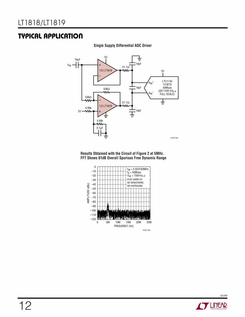
Single Supply Differential ADC Driver
Results Obtained with the Circuit of Figure 2 at 5MHz.FFT Shows 81dB Overall Spurious Free Dynamic Range
TYPICAL APPLICATIO
U
–
+1/2 LT1819
VIN
18189 TA05
18pF51.1Ω
5V
5V
AIN+ LTC1744
14 BITS50Msps
(SET FOR 2VP-PFULL SCALE)AIN
–
+
–
18pF
51.1Ω
4.99k
0.1µF
18pF
10µF
4.99k5V
1/2 LT1819
536Ω
536ΩAM
PLIT
UDE
(dBc
)
0
–10
–20
–30
–40
–50
–60
–70
–80
–90
–100
–110
–120
fIN = 5.023193MHzfS = 50MspsVIN = 750mVP-P8192 SAMPLESNO WINDOWINGNO AVERAGING
FREQUENCY (Hz)0
18189 TA06
5M 10M 15M 20M 25M

13
LT1818/LT1819
18189f
18189 SS
OUT+IN
–IN
V+
V–
R1
C
(One Amplifier)SCHE ATIC WW
SI PLIFIED
U
PACKAGE DESCRIPTIOMS8 Package
8-Lead Plastic MSOP(Reference LTC DWG # 05-08-1660)
MSOP (MS8) 0802
0.53 ± 0.015(.021 ± .006)
SEATINGPLANE
NOTE:1. DIMENSIONS IN MILLIMETER/(INCH)2. DRAWING NOT TO SCALE3. DIMENSION DOES NOT INCLUDE MOLD FLASH, PROTRUSIONS OR GATE BURRS. MOLD FLASH, PROTRUSIONS OR GATE BURRS SHALL NOT EXCEED 0.152mm (.006") PER SIDE4. DIMENSION DOES NOT INCLUDE INTERLEAD FLASH OR PROTRUSIONS. INTERLEAD FLASH OR PROTRUSIONS SHALL NOT EXCEED 0.152mm (.006") PER SIDE5. LEAD COPLANARITY (BOTTOM OF LEADS AFTER FORMING) SHALL BE 0.102mm (.004") MAX
0.18(.077)
0.254(.010)
1.10(.043)MAX
0.22 – 0.38(.009 – .015)
TYP
0.13 ± 0.076(.005 ± .003)
0.86(.034)REF
0.65(.0256)
BSC
0° – 6° TYP
DETAIL “A”
DETAIL “A”
GAUGE PLANE
1 2 3 4
4.90 ± 0.15(1.93 ± .006)
8 7 6 5
3.00 ± 0.102(.118 ± .004)
(NOTE 3)
3.00 ± 0.102(.118 ± .004)
NOTE 4
0.52(.206)REF
5.23(.206)MIN
3.2 – 3.45(.126 – .136)
0.889 ± 0.127(.035 ± .005)
RECOMMENDED SOLDER PAD LAYOUT
0.42 ± 0.04(.0165 ± .0015)
TYP
0.65(.0256)
BSC

14
LT1818/LT1819
18189f
S5 Package5-Lead Plastic SOT-23
(Reference LTC DWG # 05-08-1633)
U
PACKAGE DESCRIPTIO
1.50 – 1.75(NOTE 4)2.60 – 3.00
0.25 – 0.50TYP 5 PLCS
NOTE 3
DATUM ‘A’
0.09 – 0.20(NOTE 3) S5 SOT-23 0502
PIN ONE
2.80 – 3.10(NOTE 4)
0.95 BSC
1.90 BSC
0.90 – 1.30
0.90 – 1.450.00 – 0.150.20 BSC
0.35 – 0.55 REF
NOTE:1. DIMENSIONS ARE IN MILLIMETERS2. DRAWING NOT TO SCALE3. DIMENSIONS ARE INCLUSIVE OF PLATING4. DIMENSIONS ARE EXCLUSIVE OF MOLD FLASH AND METAL BURR5. MOLD FLASH SHALL NOT EXCEED 0.254mm6. PACKAGE EIAJ REFERENCE IS SC-74A (EIAJ)
ATTENTION: ORIGINAL SOT23-5L PACKAGE. MOST SOT23-5L PRODUCTS CONVERTED TO THIN SOT23PACKAGE, DRAWING # 05-08-1635 AFTER APPROXIMATELYAPRIL 2001 SHIP DATE
3.85 MAX
0.62MAX
0.95REF
RECOMMENDED SOLDER PAD LAYOUTPER IPC CALCULATOR
1.4 MIN2.62 REF
1.22 REF

15
LT1818/LT1819
18189f
U
PACKAGE DESCRIPTIO
Information furnished by Linear Technology Corporation is believed to be accurate and reliable.However, no responsibility is assumed for its use. Linear Technology Corporation makes no represen-tation that the interconnection of its circuits as described herein will not infringe on existing patent rights.
S8 Package8-Lead Plastic Small Outline (Narrow .150 Inch)
(Reference LTC DWG # 05-08-1610)
.016 – .050(0.406 – 1.270)
.010 – .020(0.254 – 0.508)
× 45°
0°– 8° TYP.008 – .010
(0.203 – 0.254)
SO8 0502
.053 – .069(1.346 – 1.752)
.014 – .019(0.355 – 0.483)
TYP
.004 – .010(0.101 – 0.254)
.050(1.270)
BSC
1
N
2 3 4
N/2
.150 – .157(3.810 – 3.988)
NOTE 3
8 7 6 5
.189 – .197(4.801 – 5.004)
NOTE 3
.228 – .244(5.791 – 6.197)
.245MIN
N
1 2 3 N/2
.160 ±.005
RECOMMENDED SOLDER PAD LAYOUT
.045 ±.005 .050 BSC
.030 ±.005 TYP
INCHES(MILLIMETERS)
NOTE:1. DIMENSIONS IN
2. DRAWING NOT TO SCALE3. THESE DIMENSIONS DO NOT INCLUDE MOLD FLASH OR PROTRUSIONS. MOLD FLASH OR PROTRUSIONS SHALL NOT EXCEED .006" (0.15mm)

16
LT1818/LT1819
18189f
LT/TP 0103 2K • PRINTED IN USA
LINEAR TECHNOLOGY CORPORATION 2002
RELATED PARTSPART NUMBER DESCRIPTION COMMENTS
LT1395/LT1396/LT1397 Single/Dual/Quad 400MHz Current Feedback Amplifiers 4.6mA Supply Current
LT1806/LT1807 Single/Dual 325MHz, 140V/µs Rail-to-Rail I/O Op Amps Low Noise: 3.5nV/√Hz
LT1809/LT1810 Single/Dual 180MHz, 350V/µs Rail-to-Rail I/O Op Amps Low Distortion: –90dBc at 5MHz
LT1812/LT1813/LT1814 Single/Dual/Quad 100MHz, 750V/µs Op Amps Low Power: 3.6mA Max at ±5V
LT1815/LT1816/LT1817 Single/Dual/Quad 220MHz, 1500V/µs Op Amps Programmable Supply Current
LT6203/LT6204 Dual/Quad 100MHz, Rail-to-Rail I/O Op Amps 1.9nV/√Hz Noise, 3mA Max
Linear Technology Corporation1630 McCarthy Blvd., Milpitas, CA 95035-7417(408) 432-1900 FAX: (408) 434-0507 www.linear.com
–
+1/2 LT1819
VIN
VOUT
18189 TA03
200Ω
432Ω –
+1/2 LT1819
200Ω
–3dB BANDWIDTH: 80MHz
432Ω
FREQUENCY (Hz)
0
GAIN
(dB) 10
20
25
100k 10M 100M
18189 TA04
–101M
15
5
–5 VS = ±5VTA = 25°C
80MHz, 20dB Gain Block
20dB Gain Block Frequency Response
TYPICAL APPLICATIO
U
Large-Signal Transient Response
10ns/DIV 18189 TA07
1V/DIV