lt8722 (rev. 0)
TRANSCRIPT

LT8722
1For more information www.analog.com
Rev. 0
Document Feedback
n Driving a Thermo Electric Cooler (TEC) with Fine Control n Transmit Optical Sub-Assembly (TOSA) Cooling n Erbium Doped Fiber Amplifier (EDFA) Temperature
Regulation n Photonic Integrated Circuit (PIC) Cooling n LiDAR Mirror Control n Motor Control
TYPICAL APPLICATION
FEATURES DESCRIPTION
Ultracompact 4A, 15V, Full Bridge Driver with SPI
The LT®8722 is a high performance, high efficiency, monolithic full bridge DC/DC converter. One side of the full bridge is driven by a pulse width modulation (PWM) buck power stage, while the other side of the full bridge is driven by a linear power stage. The LT8722 can deliver up to ±54W1 of power to its load while only requiring a single inductor. An integrated 25-bit digital-to-analog converter (DAC) is used to control the LT8722 output voltage. Two additional 9-bit DACs control the positive and negative output current limits. An analog output telemetry pin can be used to monitor SPI selectable parameters such as VIN, VOUT, IOUT or the LT8722 junction tempera-ture. The serial peripheral interface (SPI) can be used to configure and control the LT8722 allowing for flexibility to set the desired output voltage, output current limits, voltage limits, switching frequency and control ON/OFF behavior. The SPI operates at up to 10MHz allowing for fast readback and control. The LT8722 operates from a single 3.1V to 15V supply. Silent Switcher techniques are used to minimize EMI/EMC emissions while delivering high efficiency at high switching frequencies. The LT8722 is available in a 3mm × 3mm LQFN package.1 VTEC = ±13.5V/±4A with VIN = 15V, fSW = 1MHz
±13.5V/±4A TEC Driver
APPLICATIONS
n 25-Bit Digital Output Voltage Control n Wide Input Voltage Range: 3.1V to 15V n ±4A Output Current n High Output Power: Up to 54W1
n High Efficiency at High Frequency n 92.6% Efficiency at 4A, 15VIN, fSW = 3MHz
n SPI Interface Allows User to: n Set Output Regulation Voltage n Set Output Current Limits n Check Device Status n Enable/Disable Output
n Integrated 4A Power Switches n Silent Switcher® Architecture n Analog Output for Diagnostics/Telemetry n Adjustable and Synchronizable: 500kHz to 3MHz n Small 3mm × 3mm 18-Lead LQFN
All registered trademarks and trademarks are the property of their respective owners.
Electrical Efficiency in Cooling Configuration
fSW = 3MHzVIN = 15VRLOAD = 2.5Ω
LOAD CURRENT (A)0 1 2 3 4
5
20
35
50
65
80
95
EFFI
CIEN
CY (%
)
8722 TA01b
VIN
VIN
SCKMOSIMISO
LDR
BST
SW
SFB
AOUT
CS
VCC
VDDIOENSWENSYNC
GND
LT8722FROM SPIMASTER
8722 TA01a
TEC LOAD
+
–
TO ADC
VOUT
0.1μF
1μF
0.1μF 1μH
150nF
1μF
VIN3.1V TO 15V
VDDIO2.7V TO 6V
0.1μF4.7μF
0.1μF4.7μF

LT8722
2Rev. 0
For more information www.analog.com
PIN CONFIGURATIONABSOLUTE MAXIMUM RATINGS
VIN, SFB, LDR, EN, SW .............................. –0.3V to 15VSWEN, SYNC ............................................... –0.3V to 6VVCC ............................................................ –0.3V to 3.8VVDDIO, SCK, MOSI, CS .................................. –0.3V to 6VAOUT ............................................................. –0.3V to 6VMISO ............................................................ –0.3V to 6VBST–SW ....................................................... –0.3V to 6VOperating Junction Temperature Range (Note 2) LT8722A ............................................ –40°C to 125°CABSMAX TJ .......................................... –40°C to +150°CStorage Temperature Range .................. –65°C to 150°CMaximum Reflow (Package Body) Temperature ... 260°C
(Note 1)
18 17 16 15
6 7
TOP VIEW
LQFN PACKAGE18-LEAD (3mm × 3mm × 0.95mm)
JA = 42°C/W, /JB = 14°C/WJCBOTTOM = 9°C/W, θJCTOP = 62°C/W, ΨJT = 1.25°C/W
AND Ψ VALUES DETERMINED PER JESD51-12EXPOSED PADS (PINS 19-22) MUST BE SOLDERED TO PCB
8 9
SYNC
VCC
BST
VIN
GND
VDDIO
SWEN
SFB
VIN
GND
MIS
O
MOS
I
SCK
CS
SW SW LDR
LDR
11
10
12
13
14
4
5
3
2
1
19 EN 20 AOUT
21GND
22GND
ORDER INFORMATION
LEAD FREE FINISHPAD
FINISH
PART MARKING* PACKAGE TYPE
MSL RATING
TEMPERATURE RANGE (SEE NOTE 2)DEVICE FINISH CODE
LT8722AV#PBF Au (RoHS) LHMC e4 18 Lead (3mm × 3mm) LQFN (Laminate Package with QFN Footprint) 3 –40°C to 125°C
Contact the factory for parts specified with wider operating temperature ranges. *The temperature grade is identified by a label on the shipping container.
Tape and reel specifications. Some packages are available in 500 unit reels through designated sales channels with #TRMPBF suffix.

LT8722
3For more information www.analog.com
Rev. 0
ELECTRICAL CHARACTERISTICS The l denotes the specifications which apply over the full operating temperature range, otherwise specifications are at TA = 25°C, VIN = 15V, VDDIO = 3.3V and GND = SYNC = 0V, EN = SWEN = high unless otherwise specified. VCC has a 1μF capacitor to GND and is driven by the VCC regulator unless otherwise stated.
PARAMETER CONDITIONS MIN TYP MAX UNITS
Voltage Supplies
VIN Supply Voltage l 3.1 15 V
VIN Quiescent Current EN = 0V 15 μA
2.8 mA
VDDIO Supply Voltage Linear Power Stage ON with LDR Floating l 2.7 5.5 V
IVDDIO Supply Shutdown Current EN = 0V, VDDIO = 2.7V, MOSI/CS/SCK = 0V 0.1 0.21 0.35 mA
IVDDIO Supply Shutdown Current EN = 0V, VDDIO = 5.5V, MOSI/CS/SCK = 0V 0.1 0.27 0.45 mA
IVDDIO Supply Current EN = 15V, Linear Power Driver ON with VTEC = 0, VDDIO = 2.7V l 1.1 2 3.2 mA
IVDDIO Supply Current EN = 15V, Linear Power Driver ON with VTEC = 0, VDDIO = 5.5V l 1.7 2.8 4.2 mA
Internal Regulator (VCC Pin)
VCC Regulator Output Voltage 1 SPIS_COMMAND[9] = 1 3.473 V
VCC Regulator Output Voltage 2 SPIS_COMMAND[9] = 0 3.149 V
VCC When Overdriven If VCC Driven from External Supply Set SPIS_COMMAND[9] = 0 l 3.4 3.8 V
VCC Supply Current at 3.4V If VCC Driven from External Supply Set SPIS_COMMAND[9] = 0 3.1 mA
VCC Supply Current at 3.8V If VCC Driven from External Supply Set SPIS_COMMAND[9] = 0 3.3 mA
VCC Regulator Output Voltage 3 VIN = 3.1V, External VCC Load = 20mA l 2.7 2.9 3.1 V
VCC Current Limit VIN = 5V 66 mA
Enable Control
EN Pin Threshold EN Rising l 0.475 0.66 0.82 V
EN Pin Hysteresis 52 mV
EN Pin Leakage Current EN = 15V l –1 0 1 µA
Switching Enable Control
SWEN Pin Threshold SWEN Rising l 1.14 1.2 1.26 V
SWEN Pin Hysteresis 21 mV
SWEN Pin Pull-Down Current SWEN = 0.25V 406 µA
SWEN Pin Leakage Current SWEN = 5.5V, SPIS_STATUS = 0 l 10 28 55 µA
Undervoltage Lockout (UVLO)
VCC UVLO Rising Threshold l 1.9 2.36 2.65 V
Hysteresis 90 mV
VDDIO UVLO Rising Threshold l 2.25 2.425 2.7 V
Hysteresis 110 mV

LT8722
4Rev. 0
For more information www.analog.com
PARAMETER CONDITIONS MIN TYP MAX UNITS
Linear Output Stage
On-Resistance
Top MOSFET (M1) VIN = 15V, ILDR = 1.5A VIN = 3.1V, ILDR = 1.5A
38 40
mΩ mΩ
Bot MOSFET (M2) VIN = 15V, ILDR = 1.5A VIN = 3.1V, ILDR = 1.5A
38 40
mΩ mΩ
LDR Pin Leakage Current VIN = 15V, LDR = 0V 13.6 µA
LDR Current Sink Limit l –6.7 –4.8 –4 A
LDR Current Source Limit l 4 5.6 7.5 A
LDR Zero Voltage SPIS_DAC = 0x0, SYS_DC[1:0] = 2b11, ITEC = 0A, ENABLE_REQ = 1 7.5 V
Linear Power Loss Limit Regulation
Regulation Power for 2W Option M1 MOSFET, Sourcing Current 2.07 W
M2 MOSFET, Sinking Current 2.225 W
Regulation Power for 3W Option M1 MOSFET, Sourcing Current 2.7 W
M2 MOSFET, Sinking Current 3.0 W
Regulation Power for 3.5W Option M1 MOSFET, Sourcing Current 3.4 W
M2 MOSFET, Sinking Current 3.8 W
PWM Output Stage
On-Resistance M3, I = 1.5A 38 mΩ
M4, I = 1.5A 40 mΩ
SW Pin Leakage Current VSW = 15V –1 0 1 µA
VSW = 0V 500 µA
Min SW On-Time Internal Clock, ISW = 4A 40 ns
Min SW Off-Time Internal Clock, ISW = 1A 37 ns
External Clock, ISW = 1A 37 ns
M3 Source Current Limit VC, Max 7 10 12 A
M3 Sink Current Limit VC, Min –8 –6 –4.5 A
M4 Sink Current Limit VC, Min –10.5 –8.2 –6.5 A
PWM Oscillator Frequency
Internal Frequency Accuracy fSW = 500kHz l 459 510 561 kHz
fSW = 3000kHz l 2643 2936 3420 kHz
Internal Frequency Increment fSW = 500kHz, SW_FRQ_ADJ[1:0] = 2b01 +14.8 %
fSW = 3000kHz, SW_FRQ_ADJ[1:0] = 2b01 +12.7 %
Internal Frequency Decrement fSW = 500kHz, SW_FRQ_ADJ[1:0] = 2b10 –15.4 %
fSW = 3000kHz, SW_FRQ_ADJ[1:0] = 2b10 –13.7 %
SYNC Pin Logic Threshold Logic High 1.6 V
Logic Low 0.45 V
SYNC Pin Leakage Current VSYNC = 0V l –0.2 0 0.2 µA
VSYNC = VCC l 0 10 30 µA
ELECTRICAL CHARACTERISTICS The l denotes the specifications which apply over the full operating temperature range, otherwise specifications are at TA = 25°C, VIN = 15V, VDDIO = 3.3V and GND = SYNC = 0V, EN = SWEN = high unless otherwise specified. VCC has a 1μF capacitor to GND and is driven by the VCC regulator unless otherwise stated.

LT8722
5For more information www.analog.com
Rev. 0
PARAMETER CONDITIONS MIN TYP MAX UNITS
PWM Duty Control
20%~80% Duty Option
Max VSFB/VIN Ratio l 80 82.5 %
Min VSFB/VIN Ratio l 17.5 20 %
15%~85% Duty Option
Max VSFB/VIN Ratio l 85 89 %
Min VSFB/VIN Ratio l 13.5 15.6 %
10%~90% Duty Option
Max VSFB/VIN Ratio l 89.6 93 %
Min VSFB/VIN Ratio l 8 10.9 %
Positive Current Limit DAC (Note 4)
Resolution 9 Bits
LSB 13.3 mA
Minimum Code 0 Code
Maximum Code 462 Code
Positive Current Limit Accuracy 1 SPIS_DAC_ILIMP = 0x96, ILIMP =150 • 13.3mA 2.157 A
Positive Current Limit Accuracy 2 SPIS_DAC_ILIMP = 0x12C, ILIMP = 300 • 13.3mA 4.157 A
Negative Current Limit DAC (Note 4)
Resolution 9 Bits
LSB 13.3 mA
Minimum Code 48 Code
Maximum Code 511 Code
Negative Current Limit Accuracy SPIS_DAC_ILIMN = 0x169, ILIMN = (361–511) • 13.3mA –2.116 A
Negative Current Limit Accuracy SPIS_DAC_ILIMN = 0xD3, ILIMN = (211–511) • 13.3mA –4.077 A
Output Voltage Setpoint DAC
Resolution (No Missing Codes) (Note 5) 25 Bits
VDAC INL –900 105 900 µV
VOUT Gain Adjust, Ga VOUT = VLDR–VSFB 0.969 V/V
VOUT Regulation Accuracy VOUT = VLDR–VSFB, VIN = 15V, ILDR = 0A
VOUT < 0 SPIS_DAC = 0xFFB20000, VOUT = –11927552/224 • 1.25 • 16 • Ga –13.818 V
VOUT = 0 SPIS_DAC = 0x00000000, VOUT = 0/224 • 1.25 • 16 • Ga 0 V
VOUT > 0 SPIS_DAC = 0x00E00000, VOUT = 11927552/224 • 1.25 • 16 • Ga 13.819 V
ELECTRICAL CHARACTERISTICS The l denotes the specifications which apply over the full operating temperature range, otherwise specifications are at TA = 25°C, VIN = 15V, VDDIO = 3.3V and GND = SYNC = 0V, EN = SWEN = high unless otherwise specified. VCC has a 1μF capacitor to GND and is driven by the VCC regulator unless otherwise stated.

LT8722
6Rev. 0
For more information www.analog.com
PARAMETER CONDITIONS MIN TYP MAX UNITS
AOUT Analog Monitor
VILIMP_ZERO SPIS_DAC_ILIMP = 0x200, ILIMP = (512–512) • 13.3mA = 0A. VILIMP = V1P65 + ILIMP/8, SPIS_AMUX = 0x40
1.665 V
VILIMP_MID SPIS_DAC_ILIMP = 0x294, ILIMP = (660–512) • 13.3mA = 1.9684A. VILIMP = V1P65 + ILIMP/8, SPIS_AMUX = 0x40
1.913 V
VILIMP_HIGH SPIS_DAC_ILIMP = 0x318, ILIMP = (792–512) • 13.3mA = 3.724A. VILIMP = V1P65 + ILIMP/8, SPIS_AMUX = 0x40
2.135 V
VILIMN_ZERO SPIS_DAC_ILIMN = 0x1FF, ILIMP = (511–511) • 13.3mA = 0A. VILIMP = V1P65 + ILIMP/8, SPIS_AMUX = 0x41
1.663 V
VILIMN_MID SPIS_DAC_ILIMN = 0x174, ILIMP = (372–511) • 13.3mA = –1.8487A. VILIMP = V1P65 + ILIMP/8, SPIS_AMUX = 0x41
1.429 V
VILIMN_HIGH SPIS_DAC_ILIMN = 0xF8, ILIMP = (248–511) • 13.3mA = –3.4979A. VILIMP = V1P65 + ILIMP/8, SPIS_AMUX = 0x41
1.221 V
AOUT_DAC_NEG SPIS_DAC = 0x00E00000, AOUT_DAC_NEG =1.8 • V1P25 - 0.8 • VDAC, SPIS_AMUX=0x42
1.51 V
AOUT_DAC_ZERO SPIS_DAC = 0x00000000, AOUT_DAC_ZERO =1.8 • V1P25 - 0.8 • VDAC, SPIS_AMUX=0x42
1.263 V
AOUT_DAC_POS SPIS_DAC = 0xFF100000, AOUT_DAC_POS =1.8 • V1P25 - 0.8 • VDAC, SPIS_AMUX=0x42
0.991 V
AVOUT_NEG SPIS_DAC = 0xFFB20000, VOUT = –11927552/224 • 1.25 • 16 • Ga = –13.792V AOUT = V1P25–VOUT/16, SPIS_AMUX = 0x43
2.125 V
AVOUT_ZERO SPIS_DAC = 0x00000000, VOUT = 0V, SPIS_AMUX = 0x43 1.259 V
AOUT_DAC_POS SPIS_DAC = 0x00E00000, VOUT = +11927552/224 • 1.25 • 16 • Ga = 13.792V AOUT = V1P25–VTEC/16, SPIS_AMUX = 0x43
0.394 V
Output Current, VIMON ILDR = –1A. AOUT = V1P65 + ILDR/10, SPIS_AMUX = 0x44 1.538 V
ILDR = 0A. AOUT = V1P65 + ILDR/10, SPIS_AMUX = 0x44 1.666 V
ILDR = 1A. AOUT = V1P65 + ILDR/10, SPIS_AMUX = 0x44 1.799 V
AOUT_2P5V AOUT = 0.6 • V2P5, SPIS_AMUX = 0x45 1.5138 V
AOUT_1P25V AOUT = V1P25, SPIS_AMUX = 0x46 1.26 V
AOUT_1P65V AOUT = V1P65, SPIS_AMUX = 0x47 1.665 V
Temp Sense Voltage at 25°C Die Temp = (AOUT –1.4207)/0.0047148, SPIS_AMUX = 0x48 1.543 V
AOUT_VIN VIN = 15V, AOUT = 0.9 • V2P5–VIN/8, SPIS_AMUX = 0x49 0.3933 V
AOUT_VCC VCC = 3.4V, AOUT_VCC = 0.4 • VCC, SPIS_AMUX = 0x4A 1.36 V
AOUT_VDDIO VDDIO = 3.3V, SPIS_AMUX = 0x4B, AOUT = 0.4 • VDDIO 1.32 V
AOUT_VSFB VSFB = 15V, SPIS_AMUX = 0x4C, AOUT = (16/17) • V1P25 + VSFB/17 2.072 V
ELECTRICAL CHARACTERISTICS The l denotes the specifications which apply over the full operating temperature range, otherwise specifications are at TA = 25°C, VIN = 15V, VDDIO = 3.3V and GND = SYNC = 0V, EN = SWEN = high unless otherwise specified. VCC has a 1μF capacitor to GND and is driven by the VCC regulator unless otherwise stated.

LT8722
7For more information www.analog.com
Rev. 0
Note 1: Stresses beyond those listed under Absolute Maximum Ratings may cause permanent damage to the device. Exposure to any Absolute Maximum Rating condition for extended periods may affect device reliability and lifetime.Note 2: LT8722A is specified over the –40°C to 125°C operating junction temperature range. High Junction temperatures degrade operating lifetimes. Note the maximum ambient temperature consistent with these specifications is determined by specific operating conditions in conjunction with board layout, the rated package thermal impedance and other environmental factors.
Note 3: This IC includes overtemperature protection that is intended to protect the device during overload conditions. Junction temperature will exceed 150°C when overtemperature protection is active. Continuous operation above the specified maximum operating junction temperature will reduce lifetime.Note 4: Current flow out of LDR and into SFB is regarded as being positive. Note 5 : Guaranteed by design, not subject to test.
ELECTRICAL CHARACTERISTICS The l denotes the specifications which apply over the full operating temperature range, otherwise specifications are at TA = 25°C, VIN = 15V, VDDIO = 3.3V and GND = SYNC = 0V, EN = SWEN = high unless otherwise specified. VCC has a 1μF capacitor to GND and is driven by the VCC regulator unless otherwise stated.
PARAMETER CONDITIONS MIN TYP MAX UNITS
Serial Bus Interface and Timing Characteristics
CS, SCK, MOSI Input High Logic Level
l 0.7•VDDIO V
CS, SCK, MOSI Input Low Logic Level
l 0.3•VDDIO V
MISO Output Low Level ISINK = 1mA, VDDIO = 3.3V, 5V l 0.4 V
MISO Output High Level ISOURCE = 1mA, VDDIO = 3.3V, 5V l VDDIO–0.4 V
SCK Clock Period l 100 ns
SCK Pulse High Time l 40 ns
SCK Pulse Low Time l 40 ns
CS Falling to SCK Rising Delay Time
l 45 ns
SCK Falling to CS Rising Delay Time
l 45 ns
CS High Time l 20 ns
MOSI to SCK l 12.5 ns
MOSI to SCK l 12.5 ns
SCK to MISO, 80pF Load l 27.5 ns

LT8722
8Rev. 0
For more information www.analog.com
Figure 1. Timing Diagram for SPI
tSCK tSCKL tSCKH
tDHtDS
8722 F01
tDCS
tDV
tCSD
tCSH
CS
SCK
MOSI
MISO
TIMING DIAGRAM
LT8722
9For more information www.analog.com
Rev. 0
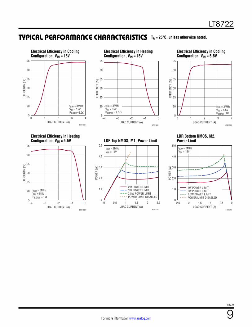
TYPICAL PERFORMANCE CHARACTERISTICS
Electrical Efficiency in Cooling Configuration, VIN = 15V
Electrical Efficiency in Heating Configuration, VIN = 15V
Electrical Efficiency in Cooling Configuration, VIN = 5.5V
Electrical Efficiency in Heating Configuration, VIN = 5.5V LDR Top NMOS, M1, Power Limit
LDR Bottom NMOS, M2, Power Limit
TA = 25°C, unless otherwise noted.
fSW = 3MHzVIN = 15VRLOAD =2.5Ω
LOAD CURRENT (A)0 1 2 3 4
5
20
35
50
65
80
95
EFFI
CIEN
CY (%
)
Cooling Efficiency, VIN = 15V
8722 G01
fSW = 3MHzVIN = 15VRLOAD = 2.5Ω
LOAD CURRENT (A)–4 –3 –2 –1 0
5
20
35
50
65
80
95
EFFI
CIEN
CY (%
)
IN
8722 G02
fSW = 3MHzVIN = 5.5VRLOAD =1Ω
LOAD CURRENT (A)0 1 2 3 4
5
20
35
50
65
80
95
EFFI
CIEN
CY (%
)
IN
8722 G03
fSW = 3MHzVIN = 5.5VRLOAD = 1Ω
LOAD CURRENT (A)–4 –3 –2 –1 0
5
20
35
50
65
80
95
EFFI
CIEN
CY (%
)
IN
8722 G04
fSW = 2MHzVIN = 15V
2W POWER LIMIT3W POWER LIMIT3.5W POWER LIMITPOWER LIMIT DISABLED
LOAD CURRENT (A)0 0.5 1 1.5 2 2.5
0
1.0
2.0
3.0
4.0
5.0
POW
ER (W
)
LDR TOP NFET POWER LIMIT
8722 G05
fSW = 2MHzVIN = 15V
2W POWER LIMIT2W POWER LIMIT3.5W POWER LIMITPOWER LIMIT DISABLED
LOAD CURRENT (A)–2.5 –2 –1.5 –1 –0.5 00
1.0
2.0
3.0
4.0
5.0
POW
ER (W
)
LDR BOTTOM NFET POWER LIMIT
8722 G06

LT8722
10Rev. 0
For more information www.analog.com
PIN FUNCTIONSVIN (Pins 4 and 11): Input Supply Pins. The VIN pins supply current to the LT8722 internal circuitry, the linear power stage as well as the buck power stage. Bypass these pins to ground with two 4.7μF capacitors and two 0.1μF capacitors as shown in Figure 15.
GND (Pins 5, 10, 21 and 22): Ground Pins. Tie directly to local ground plane.
SW (Pins 6 and 7): Switch Pins. The SW pins are the outputs of the buck stage’s internal power switches. Tie these pins together and connect them to the inductor and boost capacitor. This node should be kept small on the PCB for good performance and low EMI.
LDR (Pins 8 and 9): Linear Drive Pins. The LDR pins are the outputs of the linear stage’s internal power switches. Tie these pins together.
VCC (Pin 2): Internal 3.4V Regulator Bypass Pin. The inter-nal power drivers and control circuits are powered from this voltage. Do not load the VCC pin with external circuitry.
SYNC (Pin 1): Synchronization Pin. Clocking Modes: 1) Drive this pin with a clock source to synchronize to an external frequency. 2) Tie this pin to GND to use the inter-nal oscillator.
VDDIO (Pin 14): Serial Interface Supply Pin. The range of VDDIO is 2.7V to 5.5V. Use a minimum 0.1µF local bypass capacitor to GND on this pin.
EN (Pin 19): The LT8722 is in shutdown when both EN pin and ENABLE_REQ SPI bit are low. The LT8722 is active when either the EN pin is high or the ENABLE_REQ is high. The VCC regulator is on when the LT8722 is active. The hysteretic threshold voltage is 0.66V going up and 0.61V going down. An external resistor divider from VIN can be used to program a VIN threshold below which the EN pin will be considered low. Tie EN to GND if the EN pin
is not used. This option may allow a more substantial PCB ground connection under the LT8722, thereby keeping the LT8722 junction temperature cooler. Do not float this pin.
SWEN (Pin 13): The SWEN pin is an input/output pin. The LT8722 switching behavior can be enabled when this pin is high and is disabled when this pin is low. This pin is pulled low internally by the LT8722 when the LT8722 detects a fault. This pin can also be pulled low by an external circuit. See the Driving the SWEN Pin section for further information.
CS (Pin 15): Chip Select Input Pin. The serial data I/O bus is enabled when CS is low and disabled when CS is high.
MISO (Pin 18): Serial Data Output Pin. Output data format-ting is described in the Applications Information section.
MOSI (Pin 17): Serial Data Input Pin. Drive this pin with the desired configuration as described in the Applications Information section.
SCK (Pin 16): Serial Clock Input Pin. Drive SCK with the serial I/O clock. SCK rising edges latch serial data in on the MOSI. Capture output data from the MISO on rising edges of SCK.
BST (Pin 3): Boost Pin. This pin is used to provide a drive voltage, higher than the input voltage, to the buck stage’s topside power switch (M3). Place a 0.1µF boost capacitor from this pin to the SW pin as close to the IC as possible.
SFB (Pin 12): Switcher Feedback Pin. This pin pro-vides feedback to the buck stage for regulating the output voltage.
AOUT (Pin 20): Analog Output Pin. Internal analog signals can be buffered out to this pin by sending commands through the digital serial interface. See the Applications Information section for more information.
LT8722
11For more information www.analog.com
Rev. 0
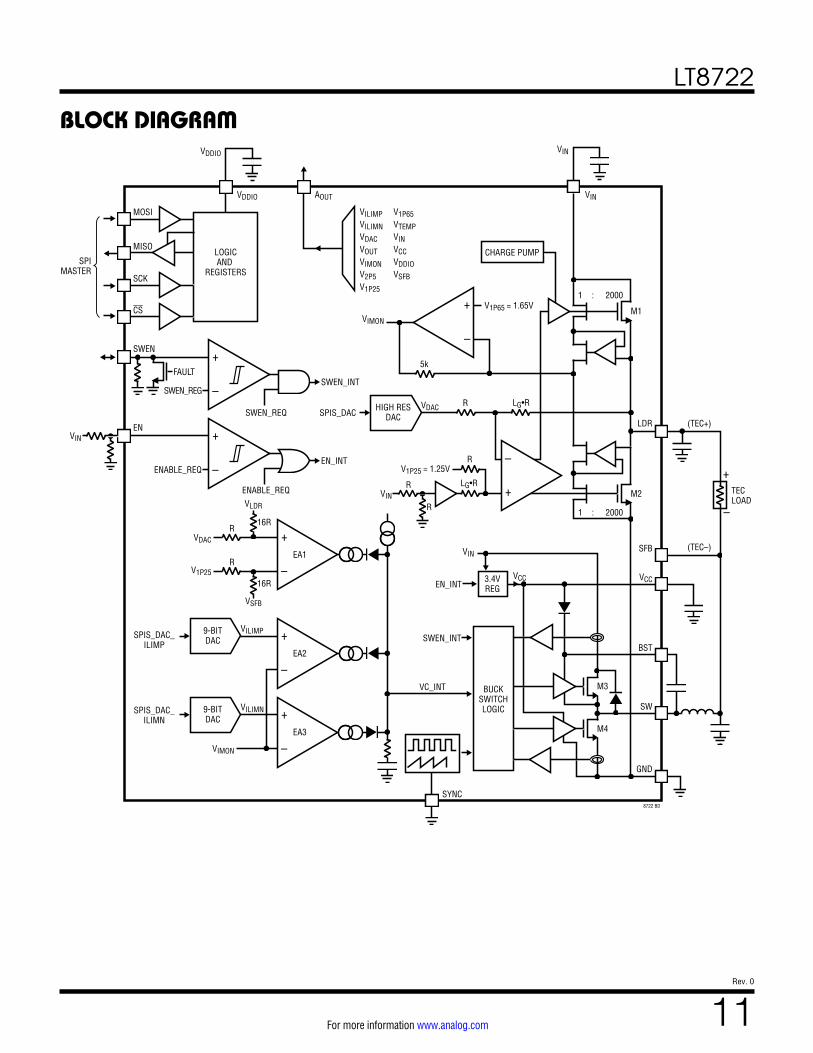
BLOCK DIAGRAM
16R
VLDR
16R
VSFB
R
R
TECLOAD
+
–
CHARGE PUMPLOGICAND
REGISTERS
MOSI
MISO
SCK
CS
SWEN
–
+
SWEN_REG
FAULT
SWEN_REQ
SWEN_INT
EN
–
+
ENABLE_REQ
ENABLE_REQ
EN_INT
SPIS_DAC_ILIMP
VIMON
–
+EA2
–
+EA1
–
+EA3
9-BITDAC
VILIMP
SPIS_DAC_ILIMN
9-BITDAC
VILIMN
VDAC
V1P25
M3
M4
M2
GND
SW
BST
VCC
SFB
LDR
(TEC–)
8722 BD
BUCKSWITCHLOGIC
SYNC
3.4VREG
SWEN_INT
EN_INT
VC_INT
VCC
VIN
R
RVIN
–
+
M1
SPIS_DACHIGH RES
DACVDAC
(TEC+)
1 : 2000
1 : 2000
LG•R
LG•R
V1P25 = 1.25VR
5k
R
–
+ V1P65 = 1.65VVIMON
VDDIO
VDDIO VIN
VINAOUT
VILIMPVILIMNVDACVOUTVIMONV2P5V1P25
V1P65VTEMPVINVCCVDDIOVSFB
VIN
SPIMASTER

LT8722
12Rev. 0
For more information www.analog.com
OPERATIONThe LT8722 is a monolithic, fixed-frequency, current-mode, full bridge DC/DC converter. Utilizing a hybrid drive system, where one side of the load employs a linear drive (LDR) while the other side of the load employs a traditional PWM switching drive (SFB). Due to this unique architecture, only a single inductor and output capacitor are required to achieve traditional full bridge drive capability.
The LT8722 comes equipped with a serial peripheral inter-face (SPI). Using the SPI, a 25-bit digital control word can be applied to the LT8722 to achieve a desired voltage at the converter output. Additional digital control informa-tion can be sent and received through the SPI to achieve the desired current limits, power limits as well as read back device status information. Setting the switching fre-quency of the LT8722 is also accomplished with sending of SPI commands. Alternatively, an external clock can be applied to the SYNC pin forcing the switching regulator drive to operate at the externally applied clock frequency.
If the EN pin is low and the ENABLE_REQ control bit is low, the LT8722 is shut down and draws ~15μA from the input. When the EN pin is above 0.74V or the ENABLE_REQ control bit is set high, the LT8722 will become pow-ered on waiting for additional SPI commands to operate begin switching. When driving the SWEN pin above 1.25V and setting the SWEN_REQ control bit high, the LT8722 will begin a switching start-up sequence further detailed in the Applications Information section of this document.
Electrical efficiency for the LT8722 is given by Equation 1.
Electrical Efficiency = 100% •Electrical Power Delivered to LT8722 VOUT Load
LT8722 Electrical Input Power
(1)
To improve efficiency across all loads, supply current to the internal circuitry can be sourced through the VCC pin by reducing the VCC voltage output to 3.1V via SPI control and overdriving VCC with 3.3V to 5.5V. Otherwise, the VCC voltage should be programmed to 3.4V and internal circuity will draw current directly from VIN.
The use of the analog output telemetry (AOUT) pin on the LT8722 is optional. This output pin can be used in con-junction with an external ADC to obtain information about various aspects of the LT8722 operation including VIN,
VLOAD, ILOAD, die temp, etc. These outputs and their scal-ing equations are included in the Applications Information section of this document.
ENABLE AND STARTUP SEQUENCE
The LT8722 is in shutdown mode with ultralow quiescent current when both the EN pin is low and the ENABLE_REQ register bit is low. The VCC LDO regulator can be activated by either pulling the EN pin high or by setting the ENABLE_REQ bit high through the SPI. The rising threshold of the EN pin comparator is 0.74V with 30mV of hysteresis.
To enable the linear driver, the SPIS_STATUS register must be cleared. This is done by writing all SPIS_STATUS registers to a value of 0. The output current monitoring circuitry and integrated charge pump, which powers the linear power stage’s top MOSFET, are enabled when the ENABLE_REQ bit is high. Clearing the latched CP_UVLO bit is required to enable the linear power driver.
Finally, the PWM driver is enabled by applying a logic high voltage to the SWEN pin (through a series 20k, or greater, resistor) and writing the SWEN_REQ register to a 1.
During LT8722 start-up, large inrush currents can occur. Using proper SPI commands and wait times, a software controlled soft-start function can be synthesized that keeps inrush current to a minimum. The following state-ments encompass the recommended start-up sequence:
• First, apply proper VIN and VDDIO voltages to the LT8722.
• Second, enable the VCC LDO and other LT8722 circuitry by raising the EN pin above the 0.74V threshold and writing the ENABLE_REQ bit to a 1.
• Third, configure the output voltage control DAC (SPIS_DAC) to 0xFF000000. This code will force the LDR pin to GND when the linear power stage is later enabled.
• Fourth, write all SPIS_STATUS registers to 0. This clears all faults and allows the linear power stage to be enabled. Due to the actions in the prior step, when the linear power stage turns on in this step, the output load will be discharged to GND. Pause between this step and the next for ~1ms to allow any prebiased out-put condition to dissipate.

LT8722
13For more information www.analog.com
Rev. 0
• Fifth, ramp the output voltage control DAC (SPIS_DAC) from code 0xFF000000 to code 0x00000000 in a con-trolled manner so that the linear driver output (LDR) ramps from GND to VIN/2. During this ramping period, both the PWM driver output (SFB) and linear driver output (LDR) move together to VIN/2. The ramp time for this controlled movement to VIN/2 should be a mini-mum of 5ms.
• Sixth, enable the PWM switching behavior by raising the SWEN pin above the 1.25V threshold and writing the SWEN_REQ bit to a 1. With both output terminals at VIN/2, the inrush current through the output load is greatly minimized. After the PWM driver switching activity is enabled, keep the output voltage control DAC (SPIS_DAC) code unchanged for a minimum of 160μs.
• Finally, the output voltage control DAC (SPIS_DAC) code can be stepped in a controlled manner to the desired code. The LDR and SFB outputs will begin to diverge from one another until the desired differential voltage is developed across the output load, the differ-ential output voltage reaches the preset voltage limit, or the output current reaches the preset current limit.
Figure 2 shows the flow chart of the enable sequence and Figure 3 shows an example of the soft-start profile where the instruction about soft-start guidance is followed.
NO
BOOTSTRAP CAPVOLTAGE REFRESH
EN PIN > 0.74V?
SUCCESSFULLY CLEARSPIS_STATUS
FAULT REGISTERS
VCC
REGULATOR ON ENABLE_REQ = 1?
YES
NO
LINEAR OUTPUTENABLED
YES
NO
YES
VIN AND VDDIO UP
8722 F02
VSFB AND VLDRDIVERGE CONTROLLED
BY VDAC
ENABLE_REQ = 1? AND SWEN > 1.125V AND SWEN_REQ = 1?
LINEAR OUTPUTSTARTS CONTROLLED
BY VDAC
Figure 2. Flow Chart of Start-Up Sequence
1/2 VIN
8722 F03
VSFB
VLDR
VSFB FOLLOWS VLDR
VOUT BUILDS UP
Figure 3. Soft-Start Profile in Cooling Mode
POWERING THE DRIVERS
The LT8722 operates at an input voltage range of 3.1V to 15V that is applied to the VIN pin and an input range of 2.7V to 6V that is applied to the VDDIO pin.
The VIN pin is the power supply for the PWM driver and the linear power driver. When configuring the power sup-ply to the VIN pin keep in mind that, at high current loads, the input voltage may drop substantially due to a voltage drop in the wires between the front end power supply and the VIN pin. Leave a proper voltage margin when design-ing the front-end power supply to maintain good perfor-mance. Minimize the trace length from the power supply to the VIN pin to help mitigate the voltage drop.
SETTING THE SWITCHING FREQUENCY
The LT8722 uses a constant frequency PWM architec-ture that can be programmed to switch from 500kHz to 3MHz through the SW_FRQ_SET register bits and further be adjusted by ±15% through the SW_FRQ_ADJ regis-ter bits. Table 1 and Table 2 show the frequency setup summary.Table 1. Switching Frequency Configuration
SW_FRQ_SET BITS SWITCHING FREQUENCY
000 500kHz
001 1MHz
010 1.5MHz
011 2MHz
100 2.5MHz
101, 110, 11 3.0MHz
OPERATION

LT8722
14Rev. 0
For more information www.analog.com
Table 2. Switching Frequency AdjustmentSW_FRQ_ADJ BITS CHANGE FROM NOMINAL
00 0%
01 +15%
10 –15%
11 0%
The operating frequency of the LT8722 PWM buck driver can also be synchronized to an external source automatically.
To synchronize to the external source, simply provide a digi-tal clock signal into the SYNC pin and the LT8722 will oper-ate at the SYNC clock frequency. The duty cycle of the SYNC clock must be between 20% and 80% for proper operation. And the SYNC frequency can always be higher than the free-running oscillator frequency but should not be less than 30% of the configured free-running oscillator frequency.
Selection of the operating frequency is a trade-off between efficiency, component size and PWM duty cycle range. The advantage of high frequency operation is that lower value and smaller size inductors and capacitors can be used. The disadvantages are lower efficiency and nar-rower duty cycle range as required by the min-on time and min-off time of the PWM driver.
BOOTSTRAP CIRCUITRY AND REFRESH PERIOD
The LT8722 integrates the bootstrap regulator to pro-vide gate drive voltage for the top MOSFET of the PWM driver (M3). The regulator generates a bootstrap voltage between the BST pin and the SW pin, which is equal to the VCC voltage.
It is recommended that an X7R or an X5R, 0.1µF ceramic capacitor is placed between the BST pin and the SW pin.
Immediately after enabling the PWM driver, the bootstrap capacitor voltage may not be high enough to drive the M3 gate. A total of 32 refresh cycles, with 5μs period, are required to charge the bootstrap capacitor before the PWM driver starts to work properly. During each refresh cycle, the M3 MOSFET is designed to be turned on first for 80ns (typ), and then the M4 MOSFET is turned on for 160ns (typ). After that, both the top and bottom MOSFETs are turned off for the rest of the refresh cycle. By doing this, the
inrush load current is minimized. Figure 4 shows the typical waveforms during the bootstrap cap voltage refresh period.
8722 F04
TOP MOSFETON
BOT MOSFETON
INDUCTORCURRENT
80ns
160ns
5μs 32 CYCLES IN TOTAL
Figure 4. Bootstrap Capacitor Voltage Refresh Cycles
VCC LDO REGULATOR
An internal low dropout (LDO) regulator produces a 3.4V supply to the VCC pin from VIN when the VCC_VREG reg-ister bit is 1. This LDO can supply enough current for the LT8722’s circuitry and must be bypassed to ground with a minimum 1µF ceramic capacitor. This bypassing is necessary to supply the high transient currents required by the PWM power MOSFET drivers.
To improve overall efficiency, an external supply between 3.4V to 3.8V can be applied to the VCC pin. When an exter-nal supply is used, the VCC_VREG register bit needs to be configured to 0. With this setting, the VCC LDO’s regula-tion voltage will be reduced to 3.1V. The VCC pin can then be overdriven with an external supply between 3.4V and 3.8V. Because the VCC target output voltage is 3.1V and because the VCC LDO can only source current, only the external supply will control the VCC pin in this situation.
SETTING INITIAL PEAK INDUCTOR CURRENT
When the PWM driver is enabled, the initial peak inductor current can cause some transient behavior to the output voltage and current for a short period of time. The optimal initial peak inductor current is different for different VIN, switching frequency and inductor values. The SW_VC_INT register bits can be used to set this initial peak current. Table 3 shows the configuration summary. When the rec-ommended startup sequence is followed, the optimal initial peak inductor current can be calculated with Equation 2.
IPEAK _INIT = VIN
4 • L • fSW (2)
OPERATION
LT8722
15For more information www.analog.com
Rev. 0
Configure the SW_VC_INT bits so the initial peak inductor current is closest to the calculated optimal value.Table 3. Initial Peak Inductor Current Control
SW_VC_INT BITS DESCRIPTION, IPEAK_INIT
000 0.251A
001 0.594A
010 0.936A
011 1.278A
100 1.62A
101 1.962A
110 2.304A
111 2.646A
LDR DRIVER INTERNAL POWER MITIGATION
In some conditions, the power dissipation of the LDR driver can be quite high. The LT8722 integrates power dissipation feedback loops to limit the maximum power dissipation of the LDR driver’s top (M1) and bottom (M2) power devices. This maximum power can be configured through the PWR_LIM_BOT and PWR_LIM_TOP regis-ters. Table 4 shows the power limit setup summary.Table 4. LDR Driver Power Limit Control for M2 MOSFET
PWR_LIM_BITSAPPROX. M1/M2
POWER DISSIPATION LIMIT
0000 2W
0101 No Limit
1010 3W
1111 3.5W
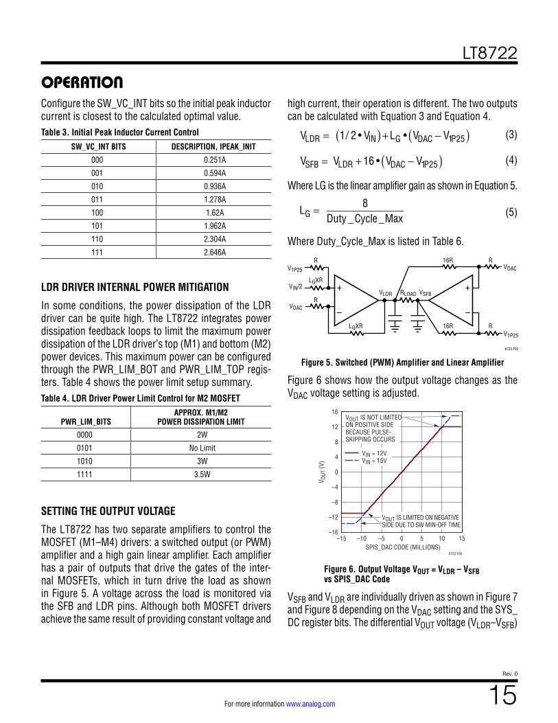
SETTING THE OUTPUT VOLTAGE
The LT8722 has two separate amplifiers to control the MOSFET (M1–M4) drivers: a switched output (or PWM) amplifier and a high gain linear amplifier. Each amplifier has a pair of outputs that drive the gates of the inter-nal MOSFETs, which in turn drive the load as shown in Figure 5. A voltage across the load is monitored via the SFB and LDR pins. Although both MOSFET drivers achieve the same result of providing constant voltage and
high current, their operation is different. The two outputs can be calculated with Equation 3 and Equation 4.
VLDR = 1/ 2 • VIN( )+LG • VDAC − V1P25( ) (3)
VSFB = VLDR +16 • VDAC − V1P25( ) (4)
Where LG is the linear amplifier gain as shown in Equation 5.
LG =
8Duty _Cycle_Max
(5)
Where Duty_Cycle_Max is listed in Table 6.
8722 F05
R
R
LGXR
V1P25
VIN/2
VDAC–
+
–
+
R
V1P25
16R
R16RLGXR
VDAC
VSFBVLDR RLOAD
Figure 5. Switched (PWM) Amplifier and Linear Amplifier
Figure 6 shows how the output voltage changes as the VDAC voltage setting is adjusted.
VOUT IS LIMITED ON NEGATIVE SIDE DUE TO SW MIN-OFF TIME
VOUT IS NOT LIMITED ON POSITIVE SIDE BECAUSE PULSE-SKIPPING OCCURS
VIN = 12VVIN = 15V
SPIS_DAC CODE (MILLIONS)–15 –10 –5 0 5 10 15
–16
–12
–8
–4
0
4
8
12
16
V OUT
(V)
8722 F06
Figure 6. Output Voltage VOUT = VLDR – VSFB vs SPIS_DAC Code
VSFB and VLDR are individually driven as shown in Figure 7 and Figure 8 depending on the VDAC setting and the SYS_DC register bits. The differential VOUT voltage (VLDR–VSFB)
OPERATION

LT8722
16Rev. 0
For more information www.analog.com
vs transfer function (Figure 6) is unaffected by SYS_DC. However, the SYS_DC register setting effects the LDR slope and the min/max duty cycle of the PWM driver as shown in Figure 7 and Figure 8.
3V = 0.2•15V
3V = 0.2•15V
VLDRVSFB
SPIS_DAC CODE (MILLIONS)–13.0 –8.7 –4.3 0.0 4.3 8.7 13.00
3
6
9
12
15
VOLT
AGE
(V)
8722 F07
Figure 7. VLDR and VSFB vs SPIS_DAC Code when VIN = 15V, SYS_DC[1:0] = 2b00, fSW = 2MHz
1.5V = 0.1•15V
1.5V = 0.1•15VVLDRVSFB
SPIS_DAC CODE (MILLIONS)–13.0 –8.7 –4.3 0.0 4.3 8.7 13.00
3
6
9
12
15
VOLT
AGE
(V)
8722 F08
Figure 8. VLDR and VSFB vs SPIS_DAC Code when VIN =15V, SYS_DC[1:0] = 2b10, fSW = 2MHz
The integrated high resolution DAC is used to set LDR, SFB and the corresponding output voltage. In a regulation feedback loop, a software controlled PID loop measures a desired parameter, then adjusts the output voltage by configuring the SPIS_DAC register through SPI. SPIS_DAC is stored in 2’s complement format. The 7MSB bits,
SPIS_DAC[31:26] are sign-extended and are decided by the SPIS_DAC[25] bit. Table 5 shows how to set VDAC through the SPIS_DAC register. Note that VDAC is equal to V1P25 when SPIS_DAC is 0x00000000. The output voltage can be calculated by Equation 6 and Equation 7.
VOUT = VLDR − VSFB = −16 • VDAC − V1P25( ) (6)
VDAC = V1P25 − SPIS_DAC • V2P5 • 2−25
(7)
The integrated 25-bit DAC is used to set the output dif-ferential voltage, VOUT, as per Equation 8. VOUT can be changed by setting the SPIS_DAC register through the SPI. SPIS_DAC is stored in 2’s complement format. The 7MSB bits, SPIS_DAC[31:26] are sign-extended and are decided by the SPIS_DAC[25] bit. Table 5 shows how to set VDAC through the SPIS_DAC register. Note that VOUT is equal to zero when SPIS_DAC is 0x00000000. The output voltage VOUT be calculated by Equation 8.
VOUT = 16 • SPIS_DAC • V2P5 • 2−25
(8)
Where 2–25 is approximately 29.802nV.Table 5. VDAC vs SPIS_DAC
SW_DAC_VTEC BITS DESCRIPTION, VDAC
0xFF000000 V1P25 + 16777216 • V2P5 • 2–25V = 2.5V
0xFF000001 V1P25 + 16777215 • V2P5 • 2–25V = 2.49999997V• • • • • •
0xFF999998 V1P25 + 6710888 • V2P5 • 2–25V = 2.00000003V
0xFF999999 V1P25 + 6710887 • V2P5 • 2–25V = 2.0V
0xFF99999A V1P25 + 6710886 • V2P5 • 2–25V = 1.99999997V• • • • • •
0xFFFFFFFF V1P25 + 1 • V2P5 • 2–25V = 1.25000003V
0x00000000 V1P25 + 0 • V2P5 • 2–25V = 1.25V
0x00000001 V1P25 – 1 • V2P5 • 2–25V = 1.24999997V• • • • • •
0x00666666 V1P25 – 6710886 • V2P5 • 2–25V = 0.75000003V
0x00666667 V1P25 – 6710887 • V2P5 • 2–25V = 0.75V
0x00666668 V1P25 – 6710888 • V2P5 • 2–25V = 0.74999997V• • • • • •
0x00FFFFFE V1P25 – 16777214 • V2P5 • 2–25V = 0.00000006V
0x00FFFFFF V1P25 – 16777215 • V2P5 • 2–25V = 0.00000003V
OPERATION
LT8722
17For more information www.analog.com
Rev. 0
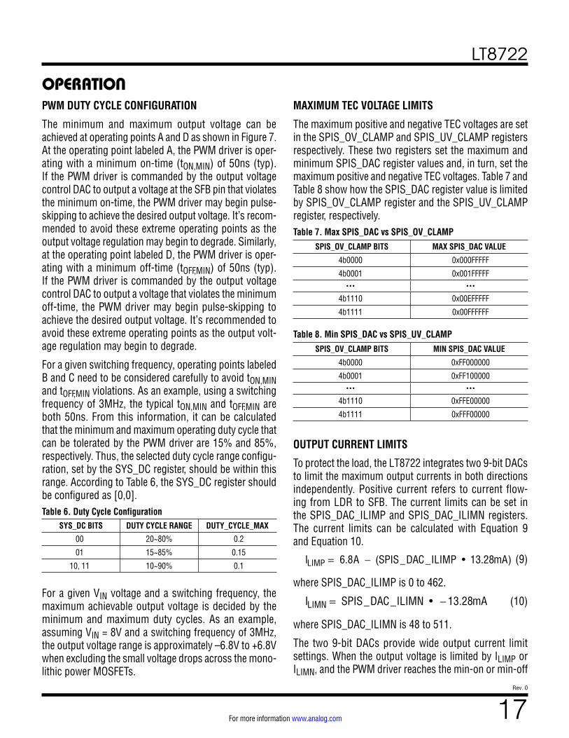
PWM DUTY CYCLE CONFIGURATION
The minimum and maximum output voltage can be achieved at operating points A and D as shown in Figure 7. At the operating point labeled A, the PWM driver is oper-ating with a minimum on-time (tON,MIN) of 50ns (typ). If the PWM driver is commanded by the output voltage control DAC to output a voltage at the SFB pin that violates the minimum on-time, the PWM driver may begin pulse-skipping to achieve the desired output voltage. It’s recom-mended to avoid these extreme operating points as the output voltage regulation may begin to degrade. Similarly, at the operating point labeled D, the PWM driver is oper-ating with a minimum off-time (tOFF,MIN) of 50ns (typ). If the PWM driver is commanded by the output voltage control DAC to output a voltage that violates the minimum off-time, the PWM driver may begin pulse-skipping to achieve the desired output voltage. It’s recommended to avoid these extreme operating points as the output volt-age regulation may begin to degrade.
For a given switching frequency, operating points labeled B and C need to be considered carefully to avoid tON,MIN and tOFF,MIN violations. As an example, using a switching frequency of 3MHz, the typical tON,MIN and tOFF,MIN are both 50ns. From this information, it can be calculated that the minimum and maximum operating duty cycle that can be tolerated by the PWM driver are 15% and 85%, respectively. Thus, the selected duty cycle range configu-ration, set by the SYS_DC register, should be within this range. According to Table 6, the SYS_DC register should be configured as [0,0]. Table 6. Duty Cycle Configuration
SYS_DC BITS DUTY CYCLE RANGE DUTY_CYCLE_MAX
00 20~80% 0.2
01 15~85% 0.15
10, 11 10~90% 0.1
For a given VIN voltage and a switching frequency, the maximum achievable output voltage is decided by the minimum and maximum duty cycles. As an example, assuming VIN = 8V and a switching frequency of 3MHz, the output voltage range is approximately –6.8V to +6.8V when excluding the small voltage drops across the mono-lithic power MOSFETs.
MAXIMUM TEC VOLTAGE LIMITS
The maximum positive and negative TEC voltages are set in the SPIS_OV_CLAMP and SPIS_UV_CLAMP registers respectively. These two registers set the maximum and minimum SPIS_DAC register values and, in turn, set the maximum positive and negative TEC voltages. Table 7 and Table 8 show how the SPIS_DAC register value is limited by SPIS_OV_CLAMP register and the SPIS_UV_CLAMP register, respectively.Table 7. Max SPIS_DAC vs SPIS_OV_CLAMP
SPIS_OV_CLAMP BITS MAX SPIS_DAC VALUE
4b0000 0x000FFFFF
4b0001 0x001FFFFF• • • • • •
4b1110 0x00EFFFFF
4b1111 0x00FFFFFF
Table 8. Min SPIS_DAC vs SPIS_UV_CLAMPSPIS_OV_CLAMP BITS MIN SPIS_DAC VALUE
4b0000 0xFF000000
4b0001 0xFF100000• • • • • •
4b1110 0xFFE00000
4b1111 0xFFF00000
OUTPUT CURRENT LIMITS
To protect the load, the LT8722 integrates two 9-bit DACs to limit the maximum output currents in both directions independently. Positive current refers to current flow-ing from LDR to SFB. The current limits can be set in the SPIS_DAC_ILIMP and SPIS_DAC_ILIMN registers. The current limits can be calculated with Equation 9 and Equation 10.
ILIMP = 6.8A − (SPIS_DAC_ILIMP • 13.28mA) (9)
where SPIS_DAC_ILIMP is 0 to 462.
ILIMN = SPIS_DAC_ILIMN • −13.28mA (10)
where SPIS_DAC_ILIMN is 48 to 511.
The two 9-bit DACs provide wide output current limit settings. When the output voltage is limited by ILIMP or ILIMN, and the PWM driver reaches the min-on or min-off
OPERATION

LT8722
18Rev. 0
For more information www.analog.com
time limitation, the PWM driver will pulse-skip cycles to maintain the desired output voltage. The purpose of this pulse-skipping is to protect the load from over current.
RESET
A reset can be triggered by system fault conditions like a VDDIO UVLO fault or a thermal shutdown fault. The SPI_RST bit can be asserted to initiate a reset, via the SPI interface, if for example an external microcontroller needs to re-initiate the system. The reset brings all registers to their default values except for the SPIS_STATUS register.
STATUS MONITORING
LT8722 status is stored in the SPIS_STATUS register summarized in Table 9. There are six fault bits: OVER_CURRENT, TSD, VCC_UVLO, VDDIO_UVLO, CP_UVLO and V2P5_UVLO. To enable the PWM driver and/or the linear driver, all fault bits must be cleared by writing each register value to 0.Table 9. SPIS_STATUS RegisterBIT NAME DESCRIPTION
SWEN 1 Indicates That the PWM is Switching
SRVO_ILIM 1 Indicates That the Output Current Limit is Active
SRVO_PLIM 1 Indicates That the Linear Regulator Power Dissipation Limiting Is Active
MIN_OT 1 Indicates That the PWM Switching Is Limited By Min-On Or Min-Off Time
POR_OCC 1 is a Latched Indicator That the Reset Has Happened Since Last Cleared
OVER_CURRENT 1 is a Latched Indicator That the Linear Driver Overcurrent Fault Has Happened Last Cleared
TSD 1 is a Latched Indicator That the Overtemperature Fault Has Happened Since Last Cleared
VCC_UVLO 1 is a Latched Indicator That the VCC Regulator UVLO Fault Has Happened Since Last Cleared
VDDIO_UVLO 1 is a Latched Indicator That the VDDIO Voltage UVLO Fault Has Happened Since Last Cleared
CP_UVLO 1 is a Latched Indicator That the Charge Pump UVLO Fault Has Happened Since Last Cleared
V2P5_UVLO 1 is a latched indicator That the 2.5V Reference UVLO Fault Has Happened Since Last Cleared
ANALOG MONITORING
Several analog signals can be monitored through the AOUT pin. The signal selection is made in the SPIS_AMUX register and is summarized in Table 10. When AOUT_EN = 0, the AOUT pin is tri-stated. The AMUX_TEST bits can be used to confirm the AOUT signal integrity by changing the AOUT pin voltage by a pre-defined amount for the selected signal. To ensure the most accurate AOUT calculation from Table 10, be sure to use the most recently measured val-ues for V1P25 and V1P65.Table 10. Analog Monitoring
AMUX[3:0] FOR MONITORING
0000 9-bit DAC Voltage, VILIMP for Positive Output Current Limit
0001 9-bit DAC Voltage, VILIMN for Negative Output Current Limit
0010 25-bit DAC Voltage, VDAC
0011 VOUT Voltage Difference, VOUT
0100 IOUT Current Information
0101 Internal Voltage Reference, V2P5
0110 Internal Voltage Reference, V1P25
0111 Internal Voltage Reference, V1P65. AOUT is Equal to V1P65 when Output Current is 0 when this Channel is Selected
1000 Chip Temperature Monitor, VTEMP
1001 VIN Voltage
1010 VCC Voltage
1011 VDDIO Voltage
1100–1101, 1110–1111
VSFB Voltage
The AOUT pin output range is 0.2V to VDDIO–0.2V. The analog MUX signal range can be beyond the AOUT pin volt-age range, so some voltage conversions are made. Output current is transformed to the voltage VIMON which is ide-ally equal to V1P65 when the output current is 0. When temperature monitoring is selected, the AOUT pin will output a voltage proportional to the die temperature with 1.498V (typ) at 25°C and a typical slope of 4.977mV/°C. Table 11 shows the AOUT pin voltage for various analog mux signals. The AMUX_TEST bits can change the AOUT pin output voltage for the same analog mux signal (see details in Table 12).
OPERATION

LT8722
19For more information www.analog.com
Rev. 0
Table 11. AOUT Voltage vs AMUX[3:0] when AMUX_TEST = 0AMUX[3:0] VOLTAGE
0000 VILIMP
0001 VILIMN
0010 V1P25 – 0.8 • VDAC
0011 V1P25 – (VLDR – VSFB)/16
0100 V1P65 – IOUT/10
0101 0.6 • V2P5
0110 V1P25
0111 V1P65
1000 VTEMP
1001 0.9 • V2P5 – VIN/8
1010 0.4 • VCC
1011 0.4 • VDDIO
1100–1111 (16/17) • V1P25 + VSFB/17
Table 12. AOUT Voltage vs AMUX[3:0] when AMUX_TEST = 1AMUX[3:0] VOLTAGE
0000–0100, 1001, 1100–1111
See Table 12
0101 (6/13) • V2P5
0110 0.8 • V1P25 + 0.2 • VCC
0111 (2/3) • V1P65
1000 0.855 • VTEMP
1010 (3/7) • VCC
1011 (4/7) • VDDIO
DRIVING THE SWEN PIN
The SWEN pin is an input/output pin. When SWEN and SWEN_REQ are high, SWEN_INT is asserted, and the SW pin begins to switch. SWEN is pulled low internally by the LT8722 when the LT8722 detects a fault. This pin can also be pulled low by an external circuit to disable switch-ing and put SW into a high impedance mode. The SWEN pin can be driven in an open-drain fashion as shown in Figure 9. The SWEN pin can be driven in a CMOS fashion as shown in Figure 10. Figure 11 shows the SWEN pin coupled to 3.3V through a 20k pull-up resistor. In this case SWEN will go high when the SPIS_STATUS[10:4] bits are cleared and FAULT goes low.
200k
20k
FAULT 1.25V
SWEN_REQ
SWEN_INT
3.3V
PULL-UPRESISTOR
OPEN-DRAINNMOS DEVICE
8722 F09
LT8722EXTERNALCIRCUITRY
SWEN+–
Figure 9. Open-Drain Drive of the SWEN Pin
200k
20k
FAULT 1.25V
SWEN_REQ
SWEN_INT
3.3V
OPTIONAL LOGICTO SENSE SWENPIN STATUS
8722 F10
LT8722EXTERNALCIRCUITRY
SWEN+–
Figure 10. CMOS Drive of the SWEN Pin
200k
20k SWEN
FAULT 1.25V
SWEN_REQ
SWEN_INT
3.3V
LT8722EXTERNALCIRCUITRY
PULL-UPRESISTOR
8722 F11
+–
Figure 11. Simple Resistor Pull-Up on the SWEN Pin
OPERATION

LT8722
20Rev. 0
For more information www.analog.com
SERIAL PERIPHERAL INTERFACE
The LT8722 utilizes an SPI slave to communicate with an external microcontroller. Through SPI, the master can configure the LT8722 functions and set parameters. The master can also read back the status of the LT8722.
The LT8722 SPI is a full duplex protocol on 4-signal lines. A clock named SCK is sent from the master to synchronize MOSI and MISO data. A chip-select enable bar signal (active low) named CS is sent from the master to enable LT8722 SPI communication. A unidirectional data line named MOSI is sent from the master to the LT8722 and a unidirectional data line named MISO is driven from the LT8722 to the master. Bits are always sent or driven MSB first. SPI Mode 0 is supported in the LT8722. In Mode 0, the SCK is low when the clock is inactive, and bits are always sampled at the rising edge of SCK and driven at the falling edge of SCK.
SPI: Packet Format
A packet is a fundamental data element composed of indi-vidual bits encoding the command, address and/or data accompanied by a CRC/ACK. Different packet types con-tain different numbers of bits. There are 3 types of packets for the LT8722 SPI: Status Acquisition, Data Write, and Data Read.
Each packet accomplishes one complete transaction over the interface, whether a Status Acquisition, Data Write, or Data Read. Packets are always initiated by pulling CS down and always end by pulling CS up.
8722 F12
CS
MOSIC[7:0] A[7:0]
ACK[7:0]00000 STATUS[10:0] CRC[7:0]MISO
CRC[7:0] 0xXX
Figure 12. Status Acquisition Packet
8722 F13
CS
MOSIC[7:0] A[7:0] CRC[7:0]
0xXX00000 STATUS[10:0] CRC[7:0] ACK[7:0]MISO
0xXX 0xXX 0xXX
0xXXD[31:24] D[23:16] D[15:8] D[7:0]
Figure 13. Data Write Packet
SPI ARCHITECTURE
8722 F14
CS
MOSIC[7:0] A[7:0] 0xXX
D[23:16]00000 STATUS[10:0] D[31:24] ACK[7:0]MISO
D[15:18] D[7:0] CRC[7:0]
0xXXCRC[7:0] 0xXX 0xXX 0xXX
Figure 14. Data Read Packet
SPI: Command
C[7:0] is an 8-bit field indicating the action that the master wants to perform as shown in Table 13.Table 13. Command Byte Description
NAME C[7:0] DESCRIPTION
SQ 0x00 Status Acquisition Command
DW 0x02 Data Write Command
DR 0x04 Data Read Command
SPI: ADDRESS
A[7:0] is an 8-bit field indicating the register address that the master wants to access. Table 14 is the register address summary and the address field duration is 8-SCK cycles. A[0] is always zero.Table 14. Address Description, A[0] Is Always Zero
ADDRESS, A[7:1] REGISTER NAME
0x00 SPIS_COMMAND
0x01 SPIS_STATUS
0x02 SPIS_DAC_ILIMN
0x03 SPIS_DAC_ILIMP
0x04 SPIS_DAC
0x05 SPIS_OV_CLAMP
0x06 SPIS_UV_CLAMP
0x07 SPIS_AMUX
SPI: DATA
D[31:0] is a 4-byte field containing the data to transfer. The data field duration is 32-SCK cycles.

LT8722
21For more information www.analog.com
Rev. 0
SUMMARY TABLEREGISTER DESCRIPTION READ/WRITE SIZE ADDRESS DEFAULT VALUE
MAIN
SPIS_COMMAND Device Control R/W 22 0x0 0x08A214
SPIS_STATUS Device Operation Summary R/W 11 0x1
DAC CONTROL
SPIS_DAC_ILIMN DAC Positive Current Limit Control Register R/W 9 0x2 0x1FF
SPIS_DAC_ILIMP DAC Negative Current Limit Control Register R/W 9 0x3 0x000
SPIS_DAC DAC Output Voltage Control Register R/W 32 0x4 0xFF000000
OV/UV CLAMP
SPIS_OV_CLAMP DAC Output Positive Voltage Limit Control Register R/W 4 0x5 0xF
SPIS_UV_CLAMP DAC Output Negative Voltage Limit Control Register
R/W 4 0x6 0x0
AMUX
SPIS_AMUX Analog MUX Control Register R/W 7 0x7 0x00
SPI REGISTER MAP
SPI: CRC
The LT8722 uses a cyclic redundancy check (CRC) to detect data communication errors in each SPI MOSI and MISO packet. The CRC in the SPI frame is an 8-bit field containing the computed CRC value spanning the com-mand, address and data. The CRC is also sent MSB first.
The default polynomial equation used for calculating the CRC is CRC-8-CCITT: X8 + X2 + X + 1. The default initial seed value for calculating the CRC is 0xFF.
SPI: Status
LT8722 SPI packets always contain Status Flags (11 bits) which are identical to the bits in the SPIS_STATUS register.
SPI ARCHITECTURESPI: Acknowledge
ACK[7:0] is an 8-bit field of 8-SCK cycles. Table 15 shows the acknowledge content.Table 15. Acknowledge Content
ACK[7:0] DESCRIPTION
0xA5 Acknowledge
0xC3 Non-Acknowledge
0x0F Reject Due to Unsupported Register Address
0x00 Stuck at 0
0xFF Stuck at 1
Others Corruption

LT8722
22Rev. 0
For more information www.analog.com
SPIS_COMMAND Register
This register is used to enable and disable the device, set the switching frequency, control the PWM output duty cycle, set the VCC voltage, set initial peak inductor
SPI REGISTER DESCRIPTIONS
current, execute the software reset and set the linear driver’s power loss regulation threshold.
BITS SYMBOL OPERATION
B[0] ENABLE_REQ VCC LDO enable bit and linear power stage enable request bit. Default: 0x0 VCC LDO is enabled when ENABLE_REQ = 1 OR the EN pin is high. Linear power stage is enabled when ENABLE_REQ = 1 and the SPIS_STATUS fault bits are cleared.
B[1] SWEN_REQ PWM switch enable request bit. Default: 0x0 1b1: Request PWM switching enable. PWM switching is enabled when SWEN_REQ = 1 and the SWEN pin is high and the VCC LDO is enabled. 1b0: PWM switching is disabled.
B[4:2] SW_FRQ_SET[2:0] PWM switch frequency control bits. Default: 0x5 3b000: 0.5MHz 3b001: 1MHz 3b010: 1.5MHz 3b011: 2MHz 3b100: 2.5MHz 3b101, 3b110, 3b111: 3MHz
B[6:5] SW_FRQ_ADJ[1:0] PWM switch frequency adjustment bits. Default: 0x0 2b00: 0% 2b01: +15% 2b10: –15% 2b11: 0%
B[8:7] SYS_DC[1:0] PWM duty cycle control bits. Default: 0x0 2b00: 20%–80% duty cycle 2b01: 15%–85% duty cycle 2b10, 2b11: 10%–90% duty cycle

LT8722
23For more information www.analog.com
Rev. 0
BITS SYMBOL OPERATION
B[9] VCC_VREG VCC LDO regulation control bit. Default: 0x1 1b1: VCC LDO regulation voltage = 3.4V 1b0: VCC LDO regulation voltage = 3.1V
B[10] Unused Must always be set to 0x0
B[13:11] SW_VC_INT[2:0] Typical peak inductor current after BST–SW refresh period control bits. Default: 0x2 3b000: 0.252A 3b001: 0.594A 3b010: 0.936A 3b011: 1.278A 3b100: 1.620A 3b101: 1.962A 3b110: 2.304A 3b111: 2.646A
B[14] SPI_RST Software reset request bit. Default: 0x0 (Active High) This register bit (write “1” to this register bit) is used to manually reset all registers (except SPIS_STATUS register) to default values
B[18:15] PWR_LIM[3:0] Linear power stage MOSFET power limit control bits. Default: 0x5 4b0000: 2W 4b0101: No Limit 4b1010: 3W 4b1111: 3.5W Other bit combinations not allowed.
B[31:19] – Ignored
SPIS_STATUS REGISTER
This register is used to store PWM out switching status, output current limit loop status, linear power loss regula-tion status, PWM output duty status, software reset event status, output over current failure status, overtemperature
SPI REGISTER DESCRIPTIONS
failure status, VCC UVLO failure status, VDDIO UVLO fail-ure status, internal charge pump UVLO failure status and internal 2.5V voltage reference UVLO failure status.
BITS SYMBOL OPERATION
B[0] SWEN Real-time PWM switching status indicator bit. Default: 0x0 1b1: PWM switching enabled 1b0: PWM switching disabled
B[1] SRVO_ILIM Real-time current limit loop status indicator bit. Default: 0x0 1b1: Operating in current limit loop 1b0: Not operating in current limit loop
B[2] SRVO_PLIM Real-time linear power stage bottom MOSFET and top MOSFET power limit loop status indicator bit. Default: 0x0 1b1: Operating in power limit loop 1b0: Not operating in power limit loop
B[3] MIN_OT Real-time PWM duty cycle status indicator bit. Default: 0x0 1b1: Operating in min or max duty cycle, 1b0: Not operating in min or max duty cycle.
B[4] POR_OCC Latched soft reset event status indicator bit. Default: 0x0 1b1: Soft reset event by SPI_RST bit or hard reset by faults happened since last cleared 1b0: Soft reset event by SPI_RST bit has not happened since last cleared

LT8722
24Rev. 0
For more information www.analog.com
BITS SYMBOL OPERATION
B[5] OVER_CURRENT Latched Output over current event status indicator bit. Default: 0x0 1b1: Output overcurrent event happened since last cleared 1b0: Output overcurrent event has not happened since last cleared
B[6] TSD Latched overtemperature event status indicator bit. Default: 0x0 1b1: Overtemperature event happened since last cleared 1b0: Overtemperature event has not happened since last cleared
B[7] VCC_UVLO Latched VCC LDO under voltage failure event status indicator bit. Default: 0x0 1b1: VCC LDO under voltage failure event happened since last cleared 1b0: VCC LDO under voltage failure event has not happened since last cleared
B[8] VDDIO_UVLO Latched VDDIO voltage under voltage failure event status indicator bit. Default: 0x0 1b1: VDDIO voltage under voltage failure event happened since last cleared 1b0: VDDIO voltage under voltage failure event has not happened since last cleared
B[9] CP_UVLO Latched charge pump power good failure event status indicator bit. Default: 0x0 1b1: Charge pump power good status failure event happened since last cleared 1b0: Charge pump power good status failure event has not happened since last cleared
B[10] V2P5_UVLO Latched V2P5 good failure event status indicator bit. Default: 0x0 1b1: V2P5 good status failure event happened since last cleared 1b0: V2P5 good status failure event has not happened since last cleared
B[31:11] – Ignored
SPIS_DAC_ILIMN REGISTER
This register is used to set negative output current limit regulation level. LT8722 current is specified down to –4A.
BITS SYMBOL OPERATION
B[8:0] SPIS_DAC_ILIMN[8:0] 9-bit DAC control register for negative output current limit. Default: 0x03FF Format: Unsigned Integer 9b000110000 = -637.44 mA [Minimum Code] 9b000110001 = -637.44 mA – 13.28 mA 9b….. 9b111111111 = -6.786 A [Maximum Code]
B[31:9] – Ignored
SPIS_DAC_ILIMP Register
This register is used to set positive output current limit regulation level. LT8722 current is specified up to 4A.
BITS SYMBOL OPERATION
B[8:0] SPIS_DAC_ILIMP[8:0] 9-bit DAC control register for positive output current limit. Default: 0x0000 Format: Unsigned Integer 9b000000000 = 6.8 A [Minimum Code] 9b000000001 = 6.8 A – 13.28 mA 9b….. 9b111001110 = 637.44 mA [Maximum Code]
B[31:9] – Ignored
SPI REGISTER DESCRIPTIONS

LT8722
25For more information www.analog.com
Rev. 0
SPIS_DAC Register
This register is used to set output voltage.
BITS SYMBOL OPERATION
B[31:0] SPIS_DAC[31:0] 25-bit DAC control register for TEC voltage difference. Default: 0xFF000000 Format: 2’s Complement. SPIS_DAC[31:25] are sign-extended bits determined by SPIS_DAC[24] and SPIS_DAC[24] is sign bit.Note: 2-25 = 29.8023x10⁻⁹
0xFF000000 = 1.25V + 16777216 • 2.5 • 2–25V = 2.5V 0xFF000001 = 1.25V + 16777215 • 2.5 • 2–25V = 2.49999997V 0x…… 0xFF999998 = 1.25V + 6710888 • 2.5 • 2–25V = 2.00000003V 0xFF999999 = 1.25V + 6710887 • 2.5 • 2–25V = 2.0V 0xFF99999A = 1.25V + 6710886 • 2.5 • 2–25V = 1.99999997 …… 0xFFFFFFFF = 1.25V + 1 • 2.5 • 2–25V = 1.25000003V 0x00000000 = 1.25V + 0 • 2.5 • 2–25V = 1.25V 0x00000001 = 1.25V – 1 • 2.5 • 2–25V = 1.24999997V …… 0x00666666 = 1.25V – 6710886 • 2.5 • 2–25V = 0.75000003V 0x00666667 = 1.25V – 6710887 • 2.5 • 2–25V = 0.75V 0x00666668 = 1.25V – 6710888 • 2.5 • 2–25V = 0.74999997V …… 0x00FFFFFE = 1.25V – 16777214 • 2.5 • 2–25V = 0.00000006V 0x00FFFFFF = 1.25V – 16777215 • 2.5 • 2–25V = 0.00000003V
SPIS_OV_CLAMP REGISTER
This register is used to set maximum positive output voltage (VLDR–VSFB).
BITS SYMBOL OPERATION
B[3:0] SPIS_OV_CLAMP[3:0]
Positive Output voltage limit register. Default: 0xF 4b0000 = Max SPIS_DAC code value is 0x000FFFFF 4b0001 = Max SPIS_DAC code value is 0x001FFFFF 4b…… 4b1110 = Max SPIS_DAC code value is 0x00EFFFFF 4b1111 = Max SPIS_DAC code value is 0x00FFFFFF
[31:5] – Reserved
SPIS_UV_CLAMP Register
This register is used to set maximum negative output voltage (VLDR–VSFB).
BITS SYMBOL OPERATION
B[3:0] SPIS_UV_CLAMP[3:0]
Negative Output voltage limit register Default: 0x0 4b0000 = Min SPIS_DAC code value is 0xFF000000 4b0001 = Min SPIS_DAC code value is 0xFF100000 4b…… 4b1110 = Min SPIS_DAC code value is 0xFFE00000 4b1111 = Min SPIS_DAC code value is 0xFFF00000
B[31:4] – Ignored
SPI REGISTER DESCRIPTIONS

LT8722
26Rev. 0
For more information www.analog.com
SPIS_AMUX Register
This register is used to enable and disable analog monitor for internal signal monitoring.
BITS SYMBOL VALUE SIGNAL DESCRIPTION
B[3:0] AMUX[3:0] 4b0000 VILIMP The 9-bit internal DAC Voltage that controls the positive Output current limit
4b0001 VILIMN The 9-bit internal DAC Voltage that controls the negative Output current limit
4b0010 V1P25 – 0.8 • VDAC Translation of the internal 25-bit DAC voltage that controls VOUT
4b0011 V1P25 – VOUT/16 Translation of the VOUT Voltage. V1P25 can be measured on channel 4b0110
4b0100 V1P65 – IOUT/10 Translation of the IOUT Current. V1P65 can be measured on channel 4b0111
4b0101 0.6 • V2P5 Translation of the V2P5 Voltage when AMUX_TEST = 2b00 or 2b10
(6/13) • V2P5 Translation of the V2P5 Voltage when AMUX_TEST = 2b01 or 2b11
4b0110 V1P25 Translation of the V1P25 Voltage when AMUX_TEST = 2b00 or 2b10
0.8 • V1P25 + 0.2 • VCC Translation of the V1P25 Voltage when AMUX_TEST = 2b01 or 2b11
4b0111 V1P65 Translation of the V1P65 Voltage when AMUX_TEST = 2b00 or 2b10
(2/3) • V1P65 Translation of the V1P65 Voltage when AMUX_TEST = 2b01 or 2b11
4b1000 VTEMP Translation of the VTEMP Voltage when AMUX_TEST = 2b00 or 2b10
0.855 • VTEMP Translation of the VTEMP Voltage when AMUX_TEST = 2b01 or 2b11
4b1001 0.9 • V2P5 – VIN/8 Translation of the VIN Input Voltage. V2P5 Can Be Measured by Using Channel 4b0110
4b1010 0.4 • VCC Translation of the VCC LDO Voltage when AMUX_TEST = 2b00 or 2b10
(3/7) • VCC Translation of the VCC LDO Voltage when AMUX_TEST = 2b01 or 2b11
4b1011 0.4 • VDDIO Translation of the VDDIO input Voltage when AMUX_TEST = 2b00 or 2b10
(4/7) • VDDIO Translation of the VDDIO input Voltage when AMUX_TEST = 2b01 or 2b11
4b1100
(16/17) • V1P25 + VSFB/17 Translation of the VSFB voltage. V1P25 Can Be Measured by Using Channel 4b0110
4b1101
4b1110
4b1111
B[5:4] AMUX_TEST[1:0] 2b00Affects Gain of AMUX[3:0] Channels 4b0101, 0110, 0111, 1000, 1010, 1011
2b10
2b01Affects Gain of AMUX[3:0] Channels 4b0101, 0110, 0111, 1000, 1010, 1011
2b11
B[6] AOUT_EN 1b0 Analog Output Buffer Disabled
1b1 Analog Output Buffer Enabled
B[31:7] – – Ignored
SPI REGISTER DESCRIPTIONS

LT8722
27For more information www.analog.com
Rev. 0
APPLICATIONS INFORMATIONINDUCTOR SELECTION
The inductor selection determines the inductor current ripple and loop dynamic responses. Larger inductance results in smaller current ripple and slower transient response as smaller inductance results in the opposite performance. To optimize the performance, trade-offs must be made between transient response speed, effi-ciency and component size. Normally the inductor cur-rent ripple is set to a value between 30% and 40% of the maximum load current (Equation 11).
L =
VSFB • VIN − VSFB( )(VIN • fSW • ΔIL)
(11)
where ΔIL is the desired inductor current ripple in Amps.
The equivalent DC resistance (DCR) inherent in the metal conductor of the inductor is also a critical factor for induc-tor selection. The DCR can account for much of the power loss in the inductor according to PLOSS = DCR • ISFB2. Using an inductor with high DCR degrades the overall efficiency significantly. In addition, there is a conducted voltage drop through the inductor because of the DCR. When the PWM amplifier is sinking current in cooling mode, this DCR voltage drop sets the minimum voltage of the amplifier a little higher by at least tens of millivolts. Similarly, the maximum PWM amplifier output voltage is a little lower by at least tens of millivolts. This voltage drop is proportional to the value of the DCR, and reduces the output voltage range across the TEC.
When selecting an inductor, ensure the saturation cur-rent rating is higher than the maximum current peak to prevent saturation. In general, ceramic multilayer induc-tors are suitable for low current applications due to small size and low DCR. When the noise level is critical, use a shielded ferrite inductor to reduce the electromagnetic interference (EMI).
SFB CAPACITOR SELECTION
The SFB capacitor determines the output voltage ripple, transient response, as well as the loop dynamic response
of the PWM driver output. Use Equation 12 to select the capacitor.
CSFB =
ΔIL(8 • fSW • ΔfSFB)
(12)
where ΔVSFB is the desired maximum SFB pin voltage ripple.
Note that the voltage caused by the product of inductor current ripple, and the capacitor equivalent series resis-tance (ESR) also adds to the total output voltage ripple. Selecting a capacitor with low ESR can increase overall regulation and efficiency performance.
Place the SFB capacitor as close to the LT8722 as possible.
LDR CAPACITOR SELECTION
To further improve systematic noise at the output of the LT8722, additional ceramic capacitors can be added at the LDR pin. Each additional capacitor should range from 10nF – 47nF, depending on application, and have very low ESR and ESL characteristics. Capacitor positions are as follows 1) between LDR – GND close to the LT8722, 2) between LDR – SFB close to the load and 3) between LDR – GND close to the load. A lower cost, lower perfor-mance alternative would be to place a 150nF capacitor between LDR – SFB close to the primary SFB capacitor.
HIGH TEMPERATURE CONSIDERATIONS
The LT8722 has two over temperature monitors. If the junction temperature exceeds ~170°C, mainly due to high VCC regulator load current, the LT8722 will enter one ther-mal shutdown mode, and the VCC regulator, linear driver and PWM driver are all disabled. Otherwise, an overtem-perature event causes the SPI register values to reset to their default values and both drivers are disabled. Either overtemperature event is latched in the thermal shutdown (TSD) register bit. The TSD threshold has 15°C hysteresis so that the LT8722 does not recover from thermal shut-down until the on-chip temperature is below 155°C. Upon recovery, the LT8722 will enter a new start-up sequence.

LT8722
28Rev. 0
For more information www.analog.com
To ensure that the LT8722 operates below the maximum junction temperature, even at high load, careful atten-tion must be paid to provide a lower θJA value for the device. Typical techniques for enhancing heat dissipation include using larger copper layers and more vias on the printed circuit board (PCB) and possibly adding a heat sink when needed.
The LT8722 LQFN package has a large exposed pad (EPAD) at the bottom that must be soldered to the ana-log ground plane on the board. Most of the device’s heat dissipates through the EPAD. Therefore, the copper layer connected to the EPAD as well as the vias on it must be optimized to conduct the heat effectively. It is recom-mended to use a large via array and distribute them evenly on the EPAD. Generally, it is more effective to increase the number of vias than to increase the diameter of the via within a limited area.
LOW EMI PCB LAYOUT AND INPUT CAPACITOR SELECTION
The LT8722 is specifically designed to minimize EMI emissions and maximize efficiency when switching at high frequencies. For optimal performance the LT8722 requires the use of multiple VIN bypass capacitors. Two small ceramic 0.1µF capacitors should be placed as close as possible to the LT8722: One of these capacitors should be tied to VIN/GND (pins 4 and 5 respectively); a sec-ond capacitor should be tied to VIN/GND (pins 11 and 10 respectively). Two ceramic 4.7μF capacitors should also be used as bypass capacitors—one of these capacitors should be placed close to pins 4 and 5 and one of these capacitors should be placed close to pins 11 and 10. See Figure 15 for a recommended PCB layout. For more detail and PCB design files refer to the demo board guide for the LT8722. Note that large, switched currents flow in the LT8722 VIN and GND pins and the input bypass capaci-tors. The loops formed by the input capacitors should be as small as possible by placing the capacitors adjacent to the VIN and GND pins on either side of the LT8722.
APPLICATIONS INFORMATIONStep-down regulators draw current from the input sup-ply in pulses with very fast rise and fall times. The input capacitor is required to reduce the resulting voltage rip-ple at the LT8722 and to force this very high frequency switching current into a tight local loop, minimizing EMI. Capacitors with small case size such as 0402 and 0603 are optimal due to their low parasitic inductance. It is best to use ceramic capacitors of type X7R or X5R. Y5V types have poor performance over temperature and applied voltage and should not be used. The input capacitors should be placed on the same side of the circuit board, and their connections should be made on that layer. The SW and BOOST nodes should be as small as possible. To keep thermal resistance low, extend the ground plane from GND as much as possible, and add thermal vias to additional ground planes within the circuit board and on the bottom side.
8722 F15
GND GND
VIN
LDRTEC+
TEC–
SFB
10
14
5
1
18 15
96
AREA OF THE HOT LOOPS (SHOWN IN RED) SHOULD BE MINIMIZED BY PLACING THE CAPACITORS AS CLOSE TO VIN/GND PINS AS POSSIBLE.
Figure 15. Recommended PCB Layout
LT8722
29For more information www.analog.com
Rev. 0
Information furnished by Analog Devices is believed to be accurate and reliable. However, no responsibility is assumed by Analog Devices for its use, nor for any infringements of patents or other rights of third parties that may result from its use. Specifications subject to change without notice. No license is granted by implication or otherwise under any patent or patent rights of Analog Devices.
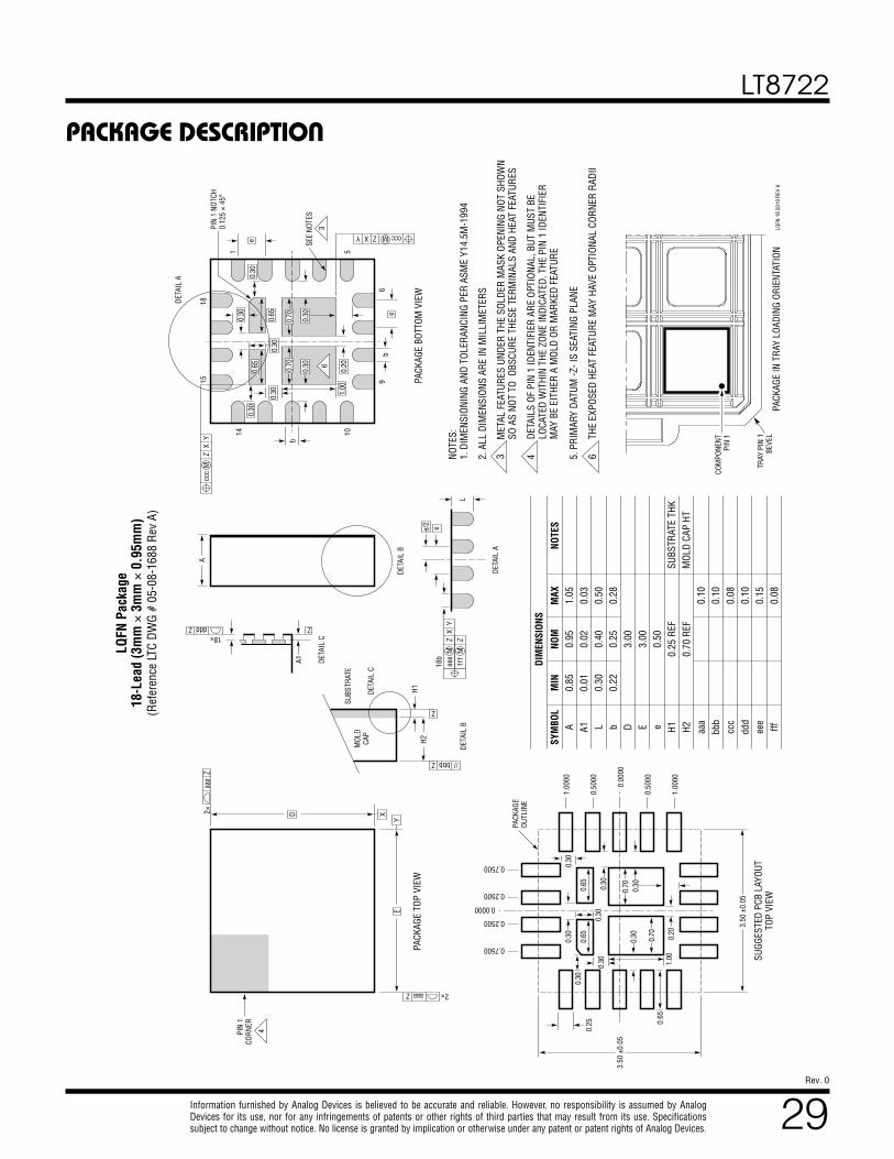
PACKAGE DESCRIPTION
4PIN
1CO
RNER
LQFN
Pac
kage
18-L
ead
(3m
m ×
3m
m ×
0.9
5mm
)(R
efer
ence
LTC
DW
G #
05-0
8-16
88 R
ev A
)
DETA
IL B
A
PACK
AGE
TOP
VIEW
X
Y
aaa
Z2×
PACK
AGE
BOTT
OM V
IEW
D
E
b
DETA
IL B
SUBS
TRAT
EM
OLD
CAP
// bbb Z
Z
H2H1DE
TAIL
C
SUGG
ESTE
D PC
B LA
YOUT
TOP
VIEW0.0000
0.00
00
1.00
00
0.50
00
0.50
00
1.00
00
0.7500
0.2500
0.2500
0.750015
18
96
1 5
14 10
aaa Z 2×
MX
YZ
ccc
MXY Z ccc
PACK
AGE
OUTL
INE
0.25 0.
65
3.50
±0.
05
3.50
±0.
05
NOTE
S:1.
DIM
ENSI
ONIN
G AN
D TO
LERA
NCIN
G PE
R AS
ME
Y14.
5M-1
994
2. A
LL D
IMEN
SION
S AR
E IN
MIL
LIM
ETER
S
MET
AL F
EATU
RES
UNDE
R TH
E SO
LDER
MAS
K OP
ENIN
G NO
T SH
OWN
SO
AS
NOT
TO O
BSCU
RE T
HESE
TER
MIN
ALS
AND
HEAT
FEA
TURE
S
5. P
RIM
ARY
DATU
M -Z
- IS
SEAT
ING
PLAN
E
43
DETA
ILS
OF P
IN 1
IDEN
TIFI
ER A
RE O
PTIO
NAL,
BUT
MUS
T BE
LO
CATE
D W
ITHI
N TH
E ZO
NE IN
DICA
TED.
THE
PIN
1 ID
ENTI
FIER
M
AY B
E EI
THER
A M
OLD
OR M
ARKE
D FE
ATUR
E
LQFN
18
0319
REV
A
TRAY
PIN
1BE
VEL
PACK
AGE
IN T
RAY
LOAD
ING
ORIE
NTAT
ION
COM
PONE
NTPI
N 1
6TH
E EX
POSE
D HE
AT F
EATU
RE M
AY H
AVE
OPTI
ONAL
COR
NER
RADI
I
DETA
IL A
ddd Z18×
18b
e
SYM
BOL
A A1 L b D E e H1 H2 aaa
bbb
ccc
ddd
eee
fff
MIN
0.85
0.01
0.30
0.22
NOM
0.95
0.02
0.40
0.25
3.00
3.00
0.50
0.25
REF
0.70
REF
MAX
1.05
0.03
0.50
0.28
0.10
0.10
0.08
0.10
0.15
0.08
NOTE
S
DIM
ENSI
ONS
Z
A1 DETA
IL C
DETA
IL A
MX
YZ
eee
MZ
fff
L
e/2
SUBS
TRAT
E TH
KM
OLD
CAP
HT
0.30
0.30
0.30
0.30
0.30
0.70
0.30
0.65
0.65
6
0.20
0.30
0.30
0.30
0.30
0.30
0.30
0.65
0.65
3
SEE
NOTE
S
be
e
PIN
1 NO
TCH
0.12
5 ×
45°
0.300.70
1.00
0.70
0.30
0.20
0.70
1.00
0.30

LT8722
30Rev. 0
For more information www.analog.com ANALOG DEVICES, INC. 2021
10/21www.analog.com
RELATED PARTS
TYPICAL APPLICATION
PART NUMBER DESCRIPTION COMMENTS
ADN8830 Thermoelectric Cooler Controller 3.0V – 5.5V Input, External MOSFETs for High Current
ADN8831 Thermoelectric Cooler Controller 3.0V – 5.5V Input, External MOSFETs for High Current
ADN8833 Ultracompact, 1A Thermoelectric Cooler (TEC) Driver for Digital Control Systems
2.7V – 5.5V Input, Integrated MOSFETs, 2.5mm × 2.5mm WLCSP or 24-Lead 4mm × 4mm LFCSP
ADN8834 Ultracompact, 1.5A Thermoelectric Cooler (TEC) Controller 2.7V – 5.5V Input, Integrated MOSFETs, 2.5mm × 2.5mm WLCSP or 24-Lead 4mm × 4mm LFCSP
ADN8835 Ultracompact, 3A Thermoelectric Cooler (TEC) Controller 2.7V – 5.5V Input, Integrated MOSFETs, 36-Lead 6mm × 6mm LFCSP
LTM4663 Ultrathin 1.5A µModule Thermoelectric Cooler (TEC) Regulator 2.7V – 5.5V Input, 3.5mm × 4mm × 1.3mm LGA Package, Very Few External Components Required
LTC1923 High Efficiency Thermoelectric Cooler Controller 2.7V – 5.5V Input, External MOSFETs for High Current, 5mm × 5mm QFN or 28-Lead SSOP
12V Input Voltage, ±4A, –11V to 12V Output, 1.5MHz TEC Driver
VIN
VIN
SCKMOSIMISO
LDR
BST
SW
SFB
AOUT
CS
VCC
SWENVDDIOENSYNC
GND
LT8722SPI CONTROLFROM μC
8722 TA02
TEC LOAD
+
–
TO ADC
VOUT
0.1μF1μF
0.1μF1μH
150nF
1μF
VIN12V
VDDIO3.3V
06030.1μF
04024.7μF
04020.1μF
06034.7μF
20k
VDDIO
OPEN-DRAIN SWENCONTROL FROM μC
fSW = 1.5MHzL: XGL4020-102MEC