ltc2393-16 - 16-bit, 1msps sar adc with 94db snr reference voltage 2.5 4.096 avp – 0.5 v refin...
TRANSCRIPT
LTC2393-16
1239316fa
TYPICAL APPLICATION
DESCRIPTION
16-Bit, 1Msps SAR ADC With 94dB SNR
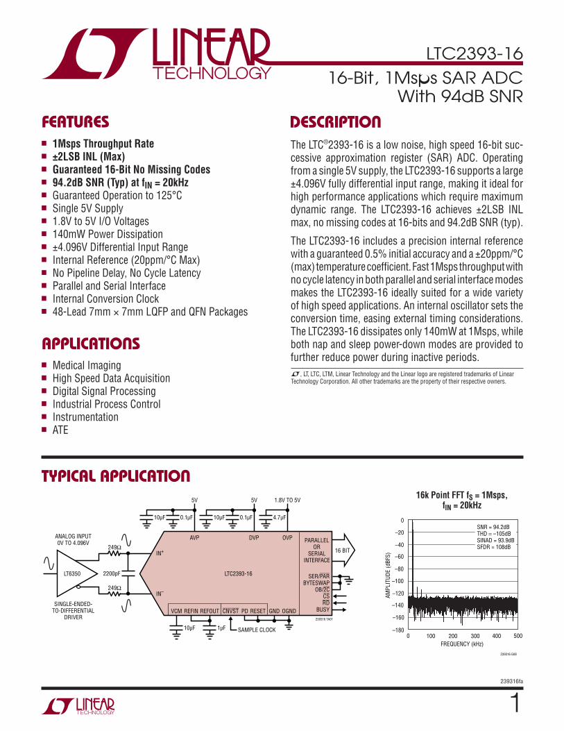
The LTC®2393-16 is a low noise, high speed 16-bit suc-cessive approximation register (SAR) ADC. Operating from a single 5V supply, the LTC2393-16 supports a large ±4.096V fully differential input range, making it ideal for high performance applications which require maximum dynamic range. The LTC2393-16 achieves ±2LSB INL max, no missing codes at 16-bits and 94.2dB SNR (typ).
The LTC2393-16 includes a precision internal reference with a guaranteed 0.5% initial accuracy and a ±20ppm/°C (max) temperature coefficient. Fast 1Msps throughput with no cycle latency in both parallel and serial interface modes makes the LTC2393-16 ideally suited for a wide variety of high speed applications. An internal oscillator sets the conversion time, easing external timing considerations. The LTC2393-16 dissipates only 140mW at 1Msps, while both nap and sleep power-down modes are provided to further reduce power during inactive periods.
FEATURES
APPLICATIONS
n 1Msps Throughput Raten ±2LSB INL (Max)n Guaranteed 16-Bit No Missing Codesn 94.2dB SNR (Typ) at fIN = 20kHzn Guaranteed Operation to 125°Cn Single 5V Supplyn 1.8V to 5V I/O Voltagesn 140mW Power Dissipationn ±4.096V Differential Input Rangen Internal Reference (20ppm/°C Max)n No Pipeline Delay, No Cycle Latencyn Parallel and Serial Interfacen Internal Conversion Clockn 48-Lead 7mm × 7mm LQFP and QFN Packages
n Medical Imagingn High Speed Data Acquisitionn Digital Signal Processingn Industrial Process Controln Instrumentationn ATE
16k Point FFT fS = 1Msps, fIN = 20kHz
FREQUENCY (kHz)
0–180
AM
PLIT
UD
E (
dB
FS)
–160
–120
–100
–80
200 400 500
0
239316 G08
–140
100 300
–60
–40
–20SNR = 94.2dBTHD –105dBSINAD = 93.9dBSFDR = 108dB
5V
0.1μF10μF
5V
0.1μF10μF
SER/PARBYTESWAP
OB/2CCS
RD
BUSY
PARALLELOR
SERIALINTERFACE
OGND
239316 TA01
IN–
IN+
2200pF
249Ω
249Ω
ANALOG INPUT0V TO 4.096V
SINGLE-ENDED-TO-DIFFERENTIAL
DRIVERGNDRESETCNVST PD
SAMPLE CLOCK
REFOUTREFIN
AVP DVP
LTC2393-16
OVP
1.8V TO 5V
16 BIT
VCM
1μF10μF
4.7μF
LT6350
L, LT, LTC, LTM, Linear Technology and the Linear logo are registered trademarks of Linear Technology Corporation. All other trademarks are the property of their respective owners.

LTC2393-16
2239316fa
Supply Voltage (VAVP , VDVP , VOVP) ..........................6.0VAnalog Input Voltage (Note 3) IN+, IN–, REFIN, CNVST .. (GND – 0.3V) to (VAVP + 0.3V)Digital Input Voltage ........ (GND – 0.3V) to (VOVP + 0.3V)Digital Output Voltage ..... (GND – 0.3V) to (VOVP + 0.3V)Power Dissipation ...............................................500mW
(Notes 1, 2)
ORDER INFORMATIONLEAD FREE FINISH TAPE AND REEL PART MARKING* PACKAGE DESCRIPTION TEMPERATURE RANGE
LTC2393CUK-16#PBF LTC2393CUK-16#TRPBF LTC2393UK-16 48-Lead 7mm × 7mm Plastic QFN 0°C to 70°C
LTC2393IUK-16#PBF LTC2393IUK-16#TRPBF LTC2393UK-16 48-Lead 7mm × 7mm Plastic QFN –40°C to 85°C
LEAD FREE FINISH TRAY PART MARKING* PACKAGE DESCRIPTION TEMPERATURE RANGE
LTC2393CLX-16#PBF LTC2393CLX-16#PBF LTC2393LX-16 48-Lead 7mm × 7mm Plastic LQFP 0°C to 70°C
LTC2393ILX-16#PBF LTC2393ILX-16#PBF LTC2393LX-16 48-Lead 7mm × 7mm Plastic LQFP –40°C to 85°C
LTC2393HLX-16#PBF LTC2393HLX-16#PBF LTC2393LX-16 48-Lead 7mm × 7mm Plastic LQFP –40°C to 125°C
Consult LTC Marketing for parts specified with wider operating temperature ranges. *The temperature grade is identified by a label on the shipping container.
Consult LTC Marketing for information on non-standard lead based finish parts.
For more information on lead free part marking, go to: http://www.linear.com/leadfree/ For more information on tape and reel specifications, go to: http://www.linear.com/tapeandreel/
ABSOLUTE MAXIMUM RATINGS
TOP VIEW
49GND
UK PACKAGE48-LEAD (7mm 7mm) PLASTIC QFN
GND 1
AVP 2
DVP 3
SER/PAR 4
GND 5
OB/2C 6
GND 7
BYTESWAP 8
D0 9
D1 10
D2 11
D3 12
36 VCM
35 GND
34 CNVST
33 PD
32 RESET
31 CS
30 RD
29 BUSY
28 D15
27 D14
26 D13
25 D12
48 G
ND
47 A
VP
46 A
VP
45 A
VP
44 G
ND
43 I
N+
42 I
N–
41 G
ND
40 A
VP
39 R
EFS
EN
SE
38 R
EFI
N
37 R
EFO
UT
D4
13
D5 1
4
D6 1
5
D7 1
6
OG
ND
17
OV
P 1
8
DV
P 1
9
GN
D 2
0
D8 2
1
D9/S
DIN
22
D10/S
DO
UT 2
3
D11/S
CLK
24
TJMAX = 125°C, θJA = 29°C/WEXPOSED PAD (PIN 49) IS GND, MUST BE SOLDERED TO PCB
123456789
101112
363534333231302928272625
GNDAVPDVP
SER/PARGND
OB/2CGND
BYTESWAPD0D1D2D3
13
14
15
16
17
18
19
20
21
22
23
24
D4
D5
D6
D7
OG
ND
OV
PD
VP
GN
DD
8D
9/S
DIN
D10/S
DO
UT
D11/S
CLK
48
47
46
45
44
43
42
41
40
39
38
37
GN
DA
VP
AV
PA
VP
GN
DIN
+
IN–
GN
DA
VP
REFS
EN
SE
REFI
NR
EFO
UT
VCMGNDCNVST
PDRESETCS
RD
BUSYD15D14D13D12
TOP VIEW
LX PACKAGE48-LEAD (7mm 7mm) PLASTIC LQFP
TJMAX = 150°C, θJA = 55°C/W
PIN CONFIGURATION
Operating Temperature Range LTC2393C ................................................ 0°C to 70°C LTC2393I.............................................. –40°C to 85°C LTC2393H .......................................... –40°C to 125°CStorage Temperature Range ................... –65°C to 150°C

LTC2393-16
3239316fa
ANALOG INPUT The l denotes the specifications which apply over the full operating temperature range, otherwise specifications are at TA = 25°C. (Note 4)
SYMBOL PARAMETER CONDITIONS MIN TYP MAX UNITS
VIN+ Absolute Input Range (IN+) (Note 5) l –0.05 AVP V
VIN– Absolute Input Range (IN–) (Note 5) l –0.05 AVP V
VIN+ – VIN
– Input Differential Voltage Range VIN = VIN+ – VIN
– l –VREF VREF V
VCM Common Mode Input Range l VREF/2 – 0.05 VREF/2 VREF/2 + 0.05 V
IIN Analog Input Leakage Current l ±1 μA
CIN Analog Input Capacitance Sample ModeHold Mode
455
pFpF
CMRR Input Common Mode Rejection Ratio 70 dB
CONVERTER CHARACTERISTICS The l denotes the specifications which apply over the full operating temperature range, otherwise specifications are at TA = 25°C. (Note 4)
SYMBOL PARAMETER CONDITIONS MIN TYP MAX UNITS
Resolution l 16 Bits
No Missing Codes l 16 Bits
Transition Noise 0.3 LSBRMS
INL Integral Linearity Error (Note 6) l –2 ±1 2 LSB
DNL Differential Linearity Error l –1 1 LSB
BZE Bipolar Zero Error (Note 7) l –7 7 LSB
Bipolar Zero Error Drift 1 ppm/°C
FSE Bipolar Full-Scale Error External ReferenceInternal Reference (Note 7)
l 0.10.1
%%
Bipolar Full-Scale Error Drift ±10 ppm/°C
DYNAMIC ACCURACY The l denotes the specifications which apply over the full operating temperature range, otherwise specifications are at TA = 25°C. AIN = –1dBFS (Notes 4, 8)
SYMBOL PARAMETER CONDITIONS MIN TYP MAX UNITS
SINAD Signal-to-(Noise + Distortion) Ratio fIN = 20kHz l 92 93.9 dB
SNR Signal-to-Noise Ratio fIN = 20kHz l 92.5 94.2 dB
THD Total Harmonic Distortion fIN = 20kHz, First 5 Harmonics (C- and I-Grades)fIN = 20kHz, First 5 Harmonics (H-Grade)
l –105–105
–100–98
dBdB
SFDR Spurious-Free Dynamic Range fIN = 20kHz 108 dB
–3dB Input Bandwidth 50 MHz
Aperture Delay 0.5 ns
Aperture Jitter 7 psRMS
Transient Response Full-Scale Step 60 ns
LTC2393-16
4239316fa
PARAMETER CONDITIONS MIN TYP MAX UNITS
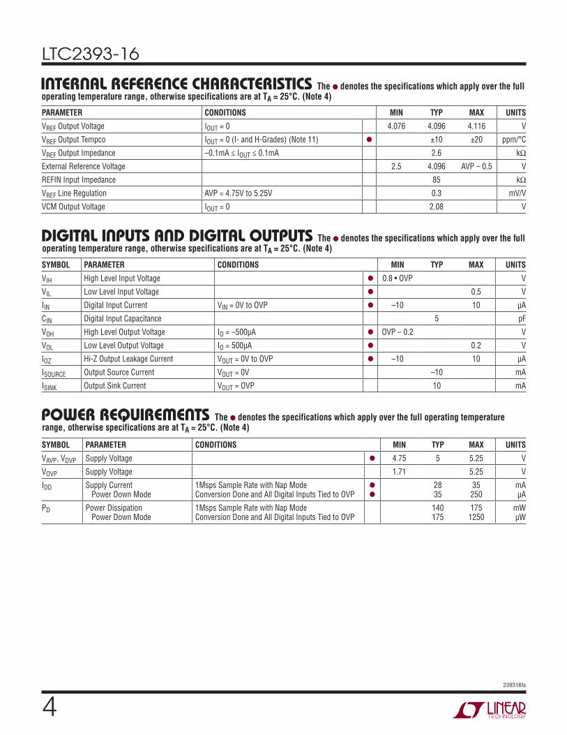
VREF Output Voltage IOUT = 0 4.076 4.096 4.116 V
VREF Output Tempco IOUT = 0 (I- and H-Grades) (Note 11) l ±10 ±20 ppm/°C
VREF Output Impedance –0.1mA ≤ IOUT ≤ 0.1mA 2.6 kΩ
External Reference Voltage 2.5 4.096 AVP – 0.5 V
REFIN Input Impedance 85 kΩ
VREF Line Regulation AVP = 4.75V to 5.25V 0.3 mV/V
VCM Output Voltage IOUT = 0 2.08 V
DIGITAL INPUTS AND DIGITAL OUTPUTS The l denotes the specifications which apply over the full operating temperature range, otherwise specifications are at TA = 25°C. (Note 4)
SYMBOL PARAMETER CONDITIONS MIN TYP MAX UNITS
VIH High Level Input Voltage l 0.8 • OVP V
VIL Low Level Input Voltage l 0.5 V
IIN Digital Input Current VIN = 0V to OVP l –10 10 μA
CIN Digital Input Capacitance 5 pF
VOH High Level Output Voltage IO = –500μA l OVP – 0.2 V
VOL Low Level Output Voltage IO = 500μA l 0.2 V
IOZ Hi-Z Output Leakage Current VOUT = 0V to OVP l –10 10 μA
ISOURCE Output Source Current VOUT = 0V –10 mA
ISINK Output Sink Current VOUT = OVP 10 mA
POWER REQUIREMENTS The l denotes the specifications which apply over the full operating temperature range, otherwise specifications are at TA = 25°C. (Note 4)
SYMBOL PARAMETER CONDITIONS MIN TYP MAX UNITS
VAVP , VDVP Supply Voltage l 4.75 5 5.25 V
VOVP Supply Voltage 1.71 5.25 V
IDD Supply Current Power Down Mode
1Msps Sample Rate with Nap Mode Conversion Done and All Digital Inputs Tied to OVP
l
l
2835
35250
mAμA
PD Power Dissipation Power Down Mode
1Msps Sample Rate with Nap Mode Conversion Done and All Digital Inputs Tied to OVP
140175
1751250
mWμW
INTERNAL REFERENCE CHARACTERISTICS The l denotes the specifications which apply over the full operating temperature range, otherwise specifications are at TA = 25°C. (Note 4)

LTC2393-16
5239316fa
TIMING CHARACTERISTICS The l denotes the specifications which apply over the full operating temperature range, otherwise specifications are at TA = 25°C. (Note 4)
SYMBOL PARAMETER CONDITIONS MIN TYP MAX UNITS
fSMPL Sampling Frequency l 1 Msps
tCONV Conversion Time l 600 ns
tACQ Acquisition Time l 385 ns
t4 CNVST Low Time l 20 ns
t5 CNVST High Time l 250 ns
t6 CNVST↓ to BUSY Delay CL = 15pF l 15 ns
t7 RESET Pulse Width l 5 ns
t8 SCLK Period (Note 9) l 12.5 ns
t9 SCLK High Time l 4 ns
t10 SCLK Low Time l 4 ns
tr , tf SCLK Rise and Fall Times (Note 10) 1 μs
t11 SDIN Setup Time l 2 ns
t12 SDIN Hold Time l 1 ns
t13 SDOUT Delay After SCLK↑ CL = 15pF l 2 8 ns
t14 SDOUT Delay After CS↓ l 8 ns
t15 CS↓ to SCLK Setup Time l 20 ns
t16 Data Valid to BUSY↓ l 1 ns
t17 Data Access Time after RD↓ or BYTESWAP↑ l 10 ns
t18 Bus Relinquish Time l 10 ns
Note 1: Stresses beyond those listed under Absolute Maximum Ratings
may cause permanent damage to the device. Exposure to any Absolute
Maximum Rating condition for extended periods may affect device
reliability and lifetime.
Note 2: All voltage values are with respect to ground.
Note 3: When these pin voltages are taken below ground or above
AVP, DVP or OVP, they will be clamped by internal diodes. This product can
handle input currents up to 100mA below ground or above AVP, DVP or
OVP without latchup.
Note 4: AVP = DVP = OVP = 5V, fSMPL = 1MHz, external reference equal to
4.096V unless otherwise noted.
Note 5: Recommended operating conditions.
Note 6: Integral nonlinearity is defined as the deviation of a code from a
straight line passing through the actual endpoints of the transfer curve.
The deviation is measured from the center of the quantization band.
Note 7: Bipolar zero error is the offset voltage measured from –0.5LSB
when the output code flickers between 0000 0000 0000 0000 and 1111
1111 1111 1111. Bipolar full-scale error is the worst-case of –FS or +FS
untrimmed deviation from ideal first and last code transitions and includes
the effect of offset error.
Note 8: All specifications in dB are referred to a full-scale ±4.096V input
with a 4.096V reference voltage.
Note 9: t13 of 8ns maximum allows a shift clock frequency up to
2 • (t13 + tSETUP) for falling edge capture with 50% duty cycle and up to
80MHz for rising capture. tSETUP is the set-up time of the receiving logic.
Note 10: Guaranteed by design.
Note 11: Temperature coefficient is calculated by dividing the maximum
change in output voltage by the specified temperature range.
4V
0.5V
50% 50%
239316F01
0.5V
4V
0.5V
4V
tDELAY
tWIDTH
tDELAY
Figure 1. Voltage Levels for Timing Specifications

LTC2393-16
6239316fa
TYPICAL PERFORMANCE CHARACTERISTICS
DC Histogram (Internal Reference)
Internal Reference Output vs Temperature Offset Error vs Temperature
Full-Scale Error vs Temperature
Integral Nonlinearity vs Output Code
Differential Nonlinearity vs Output Code
DC Histogram (External Reference)
16k Point FFT fS = 1Msps, fIN = 20kHz
OUTPUT CODE
0
INL E
RR
OR
(LS
B)
0
0.5
1.0
65536
239316 G01
–0.5
–1.0
–2.016384 32768 49152
–1.5
2.0
1.5
OUTPUT CODE
0–1.5
DN
L E
RR
OR
(LS
B)
–1.0
–0.5
0
0.5
1.0
1.5
16384 32768 49152 65536
239316 G02
TA = 25°C, fSMPL = 1Msps, unless otherwise noted.
CODE
32764
CO
UN
TS 1200000
1600000
2000000
239316 G03
800000
400000
1000000
1400000
1800000
600000
200000
032766 32768 32770 32772
CODE
32764
CO
UN
TS 1200000
1600000
2000000
239316 G04
800000
400000
1000000
1400000
1800000
600000
200000
032766 32768 32770 32772
TEMPERATURE (°C)
–55
REFE
REN
CE O
UTP
UT (
V)
4.0975
–15 25 45 125
239316 G05
4.0970
4.0965
4.0960
4.0955
4.0950
4.0945
4.0940
4.0935
4.0930
4.0925–35 5 65 85 105
TC = 4ppm/°C
TEMPERATURE (°C)
–550
OFF
SET E
RR
OR
(LS
B)
0.2
0.6
0.8
1.0
–15 25 45 125
239316 G06
0.4
–35 5 65 85 105
TEMPERATURE (°C)
–55–10
FULL-S
CA
LE E
RR
OR
(LS
B)
–8
–4
–2
0
10
4
–15 25 45 125
239316 G07
–6
6
8
2
–35 5 65 85 105
FREQUENCY (kHz)
0–180
AM
PLIT
UD
E (
dB
FS)
–160
–120
–100
–80
200 400 500
0
239316 G08
–140
100 300
–60
–40
–20SNR = 94.2dBTHD –105dBSINAD = 93.9dBSFDR = 108dB
16k Point FFT fS = 1Msps, fIN = 100kHz
FREQUENCY (kHz)
0–180
–160
AM
PLIT
UD
E (
dB
FS)
–120
–100
–80
200 400 500
0
239316 G09
–140
100 300
–60
–40
–20SNR = 94.2dBTHD –100.6dBSINAD = 93.3dBSFDR = 105.2dB

LTC2393-16
7239316fa
SNR, SINAD vs Input Level
THD, Harmonics vs Input Frequency
THD, Harmonics at fIN = 20kHz vs Temperature
Supply Current vs Sampling Frequency
Supply Current vs TemperaturePower-Down Current vs Temperature
SNR, SINAD vs Input Frequency
TYPICAL PERFORMANCE CHARACTERISTICS TA = 25°C, fSMPL = 1Msps, unless otherwise noted.
SNR, SINAD at fIN = 20kHz vs Temperature
FREQUENCY (kHz)
0
HA
RM
ON
ICS
, TH
D (
dB
FS)
–90
–85
–80
200
THD3RD
2ND
239316 G11
–95
–100
–120
–115
50 100 15025 75 125 175
–105
–110
–70
–75
TEMPERATURE (°C)
–55
SN
R, S
INA
D (
dB
FS)
93.0
94.0
94.5
95.0
SNR
–15 25 45 125
239316 G12
93.5
–35 5 65 85 105
SINAD
TEMPERATURE (°C)
–55–120
HA
RM
ON
ICS
, TH
D (
dB
FS)
–115
–105
–100
3RD
–95
–15 25 45 125
239316 G13
–110
–35 5 65 85 105
–90
THD
2ND
INPUT LEVEL (dB)
–40
SN
R, S
INA
D (
dB
FS)
94.0
94.5
0
239316 G14
93.5
93.0–30 –20 –10
95.0
SNR
SINAD
SAMPLING FREQUENCY (kHz)
10
PO
WER
SU
PP
LY C
UR
REN
T (
mA
)
20
30
5
15
25
0.1 10 100 1000
239316 G15
01
TEMPERATURE (°C)
–550
PO
WER
SU
PP
LY C
UR
REN
T (
mA
)
5
15
20
25
–15 25 45
AVP
DVP
OVP
125
239316 G16
10
–35 5 65 85 105
30
TEMPERATURE (°C)
–550
PO
WER
-DO
WN
CU
RR
EN
T (
μA
)
10
30
40
50
–15 25 45
AVP
OVP
125
239316 G17
20
–35 5 65 85 105
60
70
80
90
DVP
FREQUENCY (kHz)
0
SN
R, S
INA
D (
dB
FS)
88
92
200
239316 G10
84
8050 100 15025 75 125 175
96SNR
86
90
82
94
SINAD

LTC2393-16
8239316fa
PIN FUNCTIONSGND (Pins 1, 5, 7, 20, 35, 41, 44, 48, Exposed Pad Pin 49 (QFN Only)): Ground. All GND pins must be con-nected to a solid ground plane. Exposed pad must be soldered directly to the ground plane.
AVP (Pins 2, 40, 45, 46, 47): 5V Analog Power Supply. The range of AVP is 4.75V to 5.25V. Bypass AVP to GND with a good quality 0.1μF and a 10μF ceramic capacitor in parallel.
DVP (Pins 3, 19): 5V Digital Power Supply. The range of DVP is 4.75V to 5.25V. Bypass DVP to GND with a good quality 0.1μF and a 10μF ceramic capacitor in parallel.
SER/PAR (Pin 4): Serial/Parallel Selection Input. This pin controls the digital interface. A logic high on this pin se-lects the serial interface and a logic low selects the parallel interface. In the serial mode the non-active digital outputs are high impedance.
OB/2C (Pin 6): Offset Binary/Two’s Complement Input. When OB/2C is high, the digital output is offset binary. When low, the MSB is inverted resulting in two’s comple-ment output.
BYTESWAP (Pin 8): BYTESWAP Input. With BYTESWAP low, data will be output with Pin 28 (D15) being the MSB and Pin 9 (D0) being the LSB. With BYTESWAP high, the upper eight bits and the lower eight bits will be switched. The MSB is output on Pin 16 and Bit 8 is output on Pin 9. Bit 7 is output on Pin 28 and the LSB is output on Pin 21.
D0 (Pin 9): Data Bit 0. When SER/PAR = 0 this pin is Bit 0 of the parallel port data output bus.
D1 (Pin 10): Data Bit 1. When SER/PAR = 0 this pin is Bit 1 of the parallel port data output bus.
D2 (Pin 11): Data Bit 2. When SER/PAR = 0 this pin is Bit 2 of the parallel port data output bus.
D3 (Pin 12): Data Bit 3. When SER/PAR = 0 this pin is Bit 3 of the parallel port data output bus.
D4 (Pin 13): Data Bit 4. When SER/PAR = 0 this pin is Bit 4 of the parallel port data output bus.
D5 (Pin 14): Data Bit 5. When SER/PAR = 0 this pin is Bit 5 of the parallel port data output bus.
D6 (Pin 15): Data Bit 6. When SER/PAR = 0 this pin is Bit 6 of the parallel port data output bus.
D7 (Pin 16): Data Bit 7. When SER/PAR = 0 this pin is Bit 7 of the parallel port data output bus.
OGND (Pin 17): Digital Ground for the Input/Output Interface.
OVP (Pin 18): Digital Power Supply for the Input/Output Interface. The range for OVP is 1.8V to 5V. Bypass OVP to OGND with a good quality 4.7μF ceramic capacitor close to the pin.
D8 (Pin 21): Data Bit 8. When SER/PAR = 0 this pin is Bit 8 of the parallel port data output bus.
D9/SDIN (Pin 22): Data Bit 9/Serial Data Input. When SER/PAR = 0 this pin is Bit 9 of the parallel port data output bus. When SER/PAR = 1, (serial mode) this is the serial data input. SDIN can be used as a data input to daisy chain two or more conversion results into a single SDOUT line. The digital data level on SDIN is output on SDOUT with a delay of 16 SCLK periods after the start of the read sequence.
D10/SDOUT (Pin 23): Data Bit 10/Serial Data Output. When SER/PAR = 0 this pin is Bit 10 of the parallel port data output bus. When SER/PAR = 1, (serial mode) this is the serial data output. The conversion result can be clocked out serially on this pin synchronized to SCLK. The data is clocked out MSB first on the rising edge of SCLK and is valid on the falling edge of SCLK. The data format is determined by the logic level of OB/2C.
D11/SCLK (Pin 24): Data Bit 11/Serial Clock Input. When SER/PAR = 0 this pin is Bit 11 of the parallel port data output bus. When SER/PAR = 1, (serial mode) this is the serial clock input.
D12 (Pin 25): Data Bit 12. When SER/PAR = 0 this pin is Bit 12 of the parallel port data output bus.
D13 (Pin 26): Data Bit 13. When SER/PAR = 0 this pin is Bit 13 of the parallel port data output bus.
D14 (Pin 27): Data Bit 14. When SER/PAR = 0 this pin is Bit 14 of the parallel port data output bus.
D15 (Pin 28): Data Bit 15. When SER/PAR = 0 this pin is Bit 15 of the parallel port data output bus. The data format is determined by the logic level of OB/2C.

LTC2393-16
9239316fa
BUSY (Pin 29): Busy Output. A low-to-high transition oc-curs when a conversion is started. It stays high until the conversion is complete. The falling edge of BUSY can be used as the data-ready clock signal.
RD (Pin 30): Read Data Input. When CS and RD are both low, the parallel and serial output bus is enabled.
CS (Pin 31): Chip Select. When CS and RD are both low, the parallel and serial output bus is enabled. CS is also used to gate the external shift clock.
RESET (Pin 32): Reset Input. When high the LTC2393-16 is reset, and if this occurs during a conversion, the con-version is halted and the data bus is put into Hi-Z mode.
PD (Pin 33): Power-Down Input. When high, the LTC2393-16 is powered down and subsequent conversion requests are ignored. Before entering power shutdown, the digital output data should be read.
CNVST (Pin 34): Conversion Start Input. A falling edge on CNVST puts the internal sample-and-hold into the hold mode and starts a conversion. CNVST is independent of CS.
VCM (Pin 36): Common Mode Analog Output. Typically the output voltage is 2.048V. Bypass to GND with a 10μF capacitor.
REFOUT (Pin 37): Internal Reference Output. Nominal output voltage is 4.096V. Connect this pin to REFIN if us-ing the internal reference. If an external reference is used connect REFOUT to ground.
REFIN (Pin 38): Reference Input. An external reference can be applied to REFIN if a more accurate reference is required. If an external reference is used tie REFOUT to ground.
REFSENSE (Pin 39): Reference Input Sense. Leave REFSENSE open when using the internal reference. If an external reference is used connect REFSENSE to the ground pin of the external reference.
IN–, IN+ (Pin 42, Pin 43): Differential Analog Inputs. IN+ – (IN–) can range up to ±VREF .
PIN FUNCTIONS
LTC2393-16
10239316fa
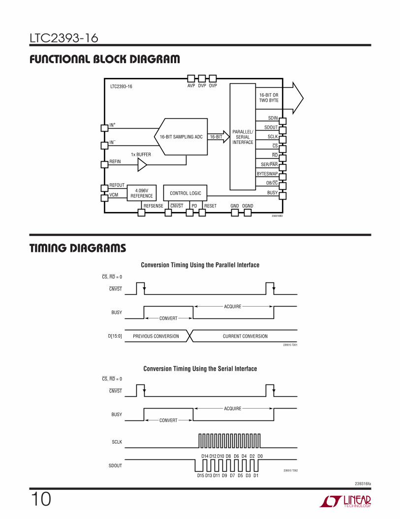
FUNCTIONAL BLOCK DIAGRAM
16-BIT SAMPLING ADCPARALLEL/
SERIALINTERFACE
SDIN
SDOUT
SCLK
CS
RD
SER/PAR
BYTESWAP
OB/2C
BUSY
239316BD
16-BIT
1x BUFFER
REFOUT
REFIN
IN–
IN+
AVPLTC2393-16 DVP OVP
VCM
REFSENSE
CONTROL LOGIC4.096V
REFERENCE
CNVST PD RESET GND OGND
16-BIT ORTWO BYTE
TIMING DIAGRAMSConversion Timing Using the Parallel Interface
CONVERT
PREVIOUS CONVERSION CURRENT CONVERSION
CNVST
CS, RD = 0
BUSY
D[15:0]
ACQUIRE
239315 TD01
Conversion Timing Using the Serial Interface
D14
D15 D13 D11 D9 D7 D5 D3
CONVERT
CNVST
CS, RD = 0
BUSY
SCLK
SDOUT
ACQUIRE
D1
239315 TD02
D12 D10 D8 D6 D4 D2 D0

LTC2393-16
11239316fa
APPLICATIONS INFORMATIONOVERVIEW
The LTC2393-16 is a low noise, high speed 16-bit suc-cessive approximation register (SAR) ADC. Operating from a single 5V supply, the LTC2393-16 supports a large ±4.096V fully differential input range, making it ideal for high performance applications which require a wide dynamic range. The LTC2393-16 achieves ±2LSB INL max, no missing codes at 16 bits and 94.2dB SNR (typ).
The LTC2393-16 includes a precision internal reference with a guaranteed 0.5% initial accuracy and a ±20ppm/°C (max) temperature coefficient. Fast 1Msps throughput with no cycle latency in both parallel and serial interface modes makes the LTC2393-16 ideally suited for a wide variety of high speed applications. An internal oscillator sets the conversion time, easing external timing considerations. The LTC2393-16 dissipates only 140mW at 1Msps, while both nap and sleep power-down modes are provided to further reduce power during inactive periods.
CONVERTER OPERATION
The LTC2393-16 operates in two phases. During the ac-quisition phase, the charge redistribution capacitor D/A converter (CDAC) is connected to the IN+ and IN– pins to sample the differential analog input voltage. A falling edge on the CNVST pin initiates a conversion. During the conversion phase, the 16-bit CDAC is sequenced through a successive approximation algorithm, effectively compar-ing the sampled input with binary-weighted fractions of the reference voltage (e.g., VREF/2, VREF/4 … VREF/65536) using the differential comparator. At the end of conversion, the CDAC output approximates the sampled analog input. The ADC control logic then prepares the 16-bit digital output code for parallel or serial transfer.
TRANSFER FUNCTION
The LTC2393-16 digitizes the full-scale voltage of 2 • VREF into 216 levels, resulting in an LSB size of 125μV when VREF = 4.096V. The ideal transfer function for two’s complement is shown in Figure 2. The OB/2C pin selects either offset binary or two’s complement format.
ANALOG INPUT
The analog inputs of the LTC2393-16 are fully differential in order to maximize the signal swing that can be digitized. The analog inputs can be modeled by the equivalent circuit shown in Figure 3. The diodes at the input provide ESD pro-tection. The analog inputs should not exceed the supply or go below ground. In the acquisition phase, each input sees approximately 40pF (CIN) from the sampling CDAC in series with 50Ω (RIN) from the on-resistance of the sampling switch. Any unwanted signal that is common to both inputs will be reduced by the common mode rejection of the ADC. The inputs draw only one small current spike while charging the CIN capacitors during acquisition. During conversion, the analog inputs draw only a small leakage current.
Figure 2. LTC2393-16 Two’s Complement Transfer Function
Figure 3. The Equivalent Circuit for the Differential Analog Input of the LTC2393-16
INPUT VOLTAGE (V)
0V
OU
TP
UT C
OD
E (
TWO
’S C
OM
PLEM
EN
T)
–1 LSB
239316 F02
011...111
011...110
000...001
000...000
100...000
100...001
111...110
1LSB
BIPOLARZERO
111...111
FSR/2 – 1LSB–FSR/2
FSR = +FS – –FS1LSB = FSR/65536
IN+RIN
CIN
AVP
AVPBIASVOLTAGE
IN–RIN
239316 F03
CIN

LTC2393-16
12239316fa
APPLICATIONS INFORMATIONINPUT DRIVE CIRCUITS
A low impedance source can directly drive the high imped-ance inputs of the LTC2393-16 without gain error. A high impedance source should be buffered to minimize settling time during acquisition and to optimize the distortion performance of the ADC.
For best performance, a buffer amplifier should be used to drive the analog inputs of the LTC2393-16. The amplifier provides low output impedance to allow for fast settling of the analog signal during the acquisition phase. It also provides isolation between the signal source and the ADC inputs which draw a small current spike during acquisition.
Input Filtering
The noise and distortion of the buffer amplifier and other circuitry must be considered since they add to the ADC noise and distortion. Noisy input circuitry should be filtered prior to the analog inputs to minimize noise. A simple 1-pole RC filter is sufficient for many applications.
Large filter RC time constants slow down the settling at the analog inputs. It is important that the overall RC time constants be short enough to allow the analog inputs to completely settle to 16-bit resolution within the acquisi-tion time (tACQ).
High quality capacitors and resistors should be used in the RC filter since these components can add distortion. NPO and silver mica type dielectric capacitors have excellent linearity. Carbon surface mount resistors can generate
distortion from self heating and from damage that may occur during soldering. Metal film surface mount resistors are much less susceptible to both problems.
Single-to-Differential Conversion
For single-ended input signals, a single-ended-to-differ-ential conversion circuit must be used to produce a dif-ferential signal at the ADC inputs. The LT6350 ADC driver is recommended for performing a single-ended-to-differential conversion, as shown in Figure 4a. Its low noise and good DC linearity allows the LTC2393-16 to meet full data sheet specifications. An alternative solution using two op amps is shown in Figure 4b. Using two LT1806 op amps, the circuit achieves 94.1dB signal-to-noise ratio (SNR). For a 20kHz input signal, the input of the LTC2393-16 has been bandwidth limited to about 25kHz.
ADC REFERENCE
A low noise, low temperature drift reference is critical to achieving the full data sheet performance of the ADC. The LTC2393-16 provides an excellent internal reference with a ±20ppm/°C (max) temperature coefficient. For better accuracy, an external reference can be used.
The high speed, low noise internal reference buffer is used for both internal and external reference applications. It cannot be bypassed.
Figure 4a. Recommended Single-Ended-to-Differential Conversion Circuit Using the LT6350 ADC Driver
249Ω
249Ω301Ω
ANALOGINPUT
0V TO 4.096V
COMMONMODE
VOLTAGE
301Ω0.013μF LTC2393-16
239316 F04b
IN+
IN–
–
+
LT1806
–
+
LT1806
249Ω
ANALOG INPUT0V TO 4.096V
SINGLE-ENDED-TO-DIFFERENTIAL
DRIVER
249Ω
2200pF LTC2393-16
239316 F04a
IN+
IN–
LT6350
Figure 4b. Alternative Single-Ended-to-Differential Conversion Circuit Using Two LT1806 Op Amps

LTC2393-16
13239316fa
APPLICATIONS INFORMATIONInternal Reference
To use the internal reference, simply tie the REFOUT and REFIN pins together. This connects the 4.096V output of the internal reference to the input of the internal reference buffer. The output impedance of the internal reference is approximately 2.6kΩ and the input impedance of the in-ternal reference buffer is about 85kΩ. It is recommended that this node be bypassed to ground with a 1μF or larger capacitor to filter the output noise of the internal reference. The REFSENSE pin should be left floating when using the internal reference.
External Reference
An external reference can be used with the LTC2393-16 when even higher performance is required. The LT1790-4.096 offers 0.05% (max) initial accuracy and 10ppm/°C (max) temperature coefficient. When using an external reference, connect the reference output to the REFIN pin and connect the REFOUT pin to ground. The REFSENSE pin should be connected to the ground of the external reference.
DYNAMIC PERFORMANCE
Fast fourier transform (FFT) techniques are used to test the ADC’s frequency response, distortion and noise at the rated throughput. By applying a low distortion sine wave and analyzing the digital output using an FFT algorithm, the ADC’s spectral content can be examined for frequen-cies outside the fundamental. The LTC2393-16 provides guaranteed tested limits for both AC distortion and noise measurements.
Signal-to-Noise and Distortion Ratio (SINAD)
The signal-to-noise and distortion ratio (SINAD) is the ratio between the RMS amplitude of the fundamental input frequency and the RMS amplitude of all other frequency components at the A/D output. The output is band-limited to frequencies from above DC and below half the sampling frequency. Figure 5 shows that the LTC2393-16 achieves a typical SINAD of 93.9dB at a 1MHz sampling rate with a 20kHz input.
Figure 5. 16k Point FFT of the LTC2393-16, fS = 1Msps, fIN = 20kHz
FREQUENCY (kHz)
0–180
AM
PLIT
UD
E (
dB
FS)
–160
–120
–100
–80
200 400 500
0
239316 G08
–140
100 300
–60
–40
–20SNR = 94.2dBTHD –105dBSINAD = 93.9dBSFDR = 108dB

LTC2393-16
14239316fa
APPLICATIONS INFORMATIONSignal-to-Noise Ratio (SNR)
The signal-to-noise ratio (SNR) is the ratio between the RMS amplitude of the fundamental input frequency and the RMS amplitude of all other frequency components except the first five harmonics and DC. Figure 5 shows that the LTC2393-16 achieves a typical SNR of 94.2dB at a 1MHz sampling rate with a 20kHz input.
Total Harmonic Distortion (THD)
Total harmonic distortion (THD) is the ratio of the RMS sum of all harmonics of the input signal to the fundamental itself. The out-of-band harmonics alias into the frequency band between DC and half the sampling frequency (fSMPL/2). THD is expressed as:
THD = 20 log
V22 + V3
2 + V42...VN
2
V1
where V1 is the RMS amplitude of the fundamental fre-quency and V2 through VN are the amplitudes of the second through Nth harmonics.
POWER CONSIDERATIONS
The LTC2393-16 provides three sets of power supply pins: the analog 5V power supply (AVP), the digital 5V power supply (DVP) and the digital input/output interface power supply (OVP). The flexible OVP supply allows the LTC2393-16 to communicate with any digital logic operating between 1.8V and 5V, including 2.5V and 3.3V systems.
Power Supply Sequencing
The LTC2393-16 does not have any specific power supply sequencing requirements. Care should be taken to observe the maximum voltage relationships described in the Ab-solute Maximum Ratings section. The LTC2393-16 has a power-on-reset (POR) circuit. With the POR, the result of the first conversion is valid after power has been applied to the ADC. The LTC2393-16 will reset itself if the power supply voltage drops below 2.5V. Once the supply voltage is brought back to its nominal value, the POR will reinitial-ize the ADC and it will be ready to start a new conversion.
Nap Mode
The LTC2393-16 can be put into the nap mode after a conversion has been completed to reduce the power consumption between conversions. In this mode some of the circuitry on the device is turned off. Nap mode is enabled by keeping CNVST low between conversions. When the next conversion is requested, bring CNVST high and hold for at least 250ns, then start the next conversion by bringing CNVST low. See Figure 6.
Power Shutdown Mode
When PD is tied high, the LTC2393-16 enters power shut-down and subsequent requests for conversion are ignored. Before entering power shutdown, the digital output data needs to be read. However, if a request for power shutdown (PD = high) occurs during a conversion, the conversion
Figure 6. Nap Mode Timing for the LTC2393-16
CNVST
BUSY
NAP
tCONV tACQ
NAP MODE
239316 F06
t5

LTC2393-16
15239316fa
APPLICATIONS INFORMATIONwill finish and then the device will power down. The data from that conversion can be read after PD = low is applied. In this mode power consumption drops to a typical value of 175μW from 140mW. This mode can be used if the LTC2393-16 is inactive for a long period of time and the user wants to minimize the power dissipation.
Recovery from Power Shutdown Mode
Once the PD pin is returned to a low level, ending the power shutdown request, the internal circuitry will begin to power up. If the internal reference is used, the 2.6kΩ output impedance with the 1μF bypass capacitor on the REFIN/REFOUT pins will be the main time constant for the power-on recovery time. If an external reference is used, typically allow 5ms for recovery before initiating a new conversion.
Power Dissipation vs Sampling Frequency
The power dissipation of the LTC2393-16 will decrease as the sampling frequency is reduced when nap mode is activated. See Figure 7. In nap mode, a portion of the circuitry on the LTC2393-16 is turned off after a conversion has been completed. Increasing the time allowed between conversions lowers the average power.
TIMING AND CONTROL
The LTC2393-16 conversion is controlled by CNVST. A falling edge on CNVST will start a conversion. CS and RD control the digital interface on the LTC2393-16. When either CS or RD is high, the digital outputs are highimpedance.
CNVST Timing
The LTC2393-16 conversion is controlled by CNVST. A falling edge on CNVST will start a conversion. Once a conversion has been initiated, it cannot be restarted until the conversion is complete. For optimum performance CNVST should be a clean low jitter signal. Converter status is indicated by the BUSY output which remains high while the conversion is in progress. To ensure no errors occur in the digitized results return the rising edge either within 40ns from the start of the conversion or wait until after the conversion has been completed. The CNVST timing needed to take advantage of the reduced power mode of operation is described in the Nap Mode section.
Internal Conversion Clock
The LTC2393-16 has an internal clock that is trimmed to achieve a maximum conversion time of 600ns. No external adjustments are required and with a maximum acquisition time of 385ns, a throughput performance of 1Msps is guaranteed.
DIGITAL INTERFACE
The LTC2393-16 allows both parallel and serial digital interfaces. The flexible OVP supply allows the LTC2393-16 to communicate with any digital logic operating between 1.8V and 5V, including 2.5V and 3.3V systems.
Figure 7. Power Dissipation of the LTC2393-16 Decreases with Decreasing Sampling Frequency
SAMPLING FREQUENCY (kHz)
10
PO
WER
SU
PP
LY C
UR
REN
T (
mA
)
20
30
5
15
25
0.1 10 100 1000
239316 G15
01

LTC2393-16
16239316fa
APPLICATIONS INFORMATIONParallel Modes
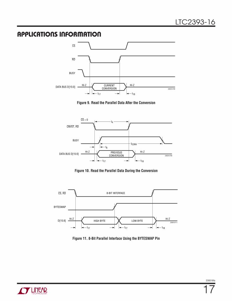
The parallel output data interface is active when the SER/PAR pin is tied low and when both CS and RD are low. The output data can be read as a 16-bit word as shown in Figures 8, 9 and 10 or it can be read as two 8-bit bytes by using the BYTESWAP pin. As shown in Figure 11, with the BYTESWAP pin low, the first eight MSBs are output on the D15 to D8 pins and the eight LSBs are output on the D7 to DO pins. When BYTESWAP is taken high, the eight LSBs now are output on the D15 to D8 pins and the eight MSBs are output on the D7 to D0 pins.
Serial Modes
The serial output data interface is active when the SER/PAR pin is tied high and when both CS and RD are low. The serial output data will be clocked out on the SDOUT pin when an external clock is applied to the SCLK pin. Clocking out the data after the conversion will yield the best performance. With a shift clock frequency of at least 40MHz, a 1Msps throughput is still achieved. The serial output data changes state on the rising edge of SCLK and can be captured on the falling edge of SCLK. D15 remains valid till the first rising edge of shift clock after the first falling edge of shift clock. The non-active digital outputs are high impedance when operating in the serial mode.
If CS and RD are used to gate the serial output data, the full conversion result should be read before CS and RD are returned to a high level.
The SDIN input pin is used to daisy chain multiple con-verters. This is useful for applications where hardware constraints may limit the number of lines needed to interface to a large number of converters. For example, if two devices are cascaded, the MSB of the first device will appear at the output after 17 SCLK cycles. The first MSB is clocked in on the falling edge of the first SCLK. See Figure 12.
Data Format
When OB/2C is high, the digital output is offset binary. When low, the MSB is inverted resulting in two’s comple-ment output. This pin is active in both the parallel and serial modes of operation.
Reset
When the RESET pin is high, the LTC2393-16 is reset, and if this occurs during a conversion, the conversion is halted and the data bus is put into Hi-Z mode. In reset, requests for new conversions are ignored. Once RESET returns low, the LTC2393-16 is ready to start a new conversion after the acquisition time has been met. See Figure 13.
Figure 8. Read the Parallel Data Continuously. The Data Bus is Always Driven and Can’t Be Shared
CS = RD = 0
t4
t6 t16
tCONV
CNVST
BUSY
DATA BUS D[15:0] PREVIOUS CONVERSION NEW
239316 F08
LTC2393-16
17239316fa
APPLICATIONS INFORMATION
Figure 9. Read the Parallel Data After the Conversion
Figure 10. Read the Parallel Data During the Conversion
Figure 11. 8-Bit Parallel Interface Using the BYTESWAP Pin
RD
BUSY
DATA BUS D[15:0]Hi-Z CURRENT
CONVERSION
t17 t18
239316 F09
Hi-Z
CS
CS = 0
CNVST, RD
BUSY
DATA BUS D[15:0]Hi-Z
t6
t17 t18
t4
tCONV
PREVIOUSCONVERSION
Hi-Z
239316 F09
CS, RD
BYTESWAP
D[15:8] HIGH BYTE LOW BYTE
8-BIT INTERFACE
Hi-Z Hi-Z
239316 F11
t17 t17 t18

LTC2393-16
18239316fa
RD = 0
CS
BUSY
t15
SCLK STARTS LOW
SCLK STARTS HIGH
t9t10
t13
1 2 3
D152
D151 D141 D131 D11 D01
239316 F12
D142 D132 D12 D02 D151 D141
4 15 16 17 18
t8
SCLK
SDOUT(ADC 2)
Hi-Z
SDIN(ADC 2)
t12t14
t11
RD = 0
CS
BUSY
t9t10
t13
1 2 3
D152
D151 D141 D131 D11 D01
D142 D132 D12 D02 D151 D141
4 15 16 17 18
t8
SCLK
SDOUT(ADC 2)
Hi-Z
SDIN(ADC 2)
t12t14
t11
LTC2393-16
ADC 1 ADC 2
SDOUT
CNVST INCS INRD IN
SCLK IN
CNVST
CS
RD
SCLKSDIN
LTC2393-16
SDOUT DATA OUT
CNVST
CS
RD
SCLKSDIN
APPLICATIONS INFORMATION
Figure 12. Serial Interface with External Clock. Read After the Conversion. Daisy Chain Multiple Converters
Figure 13. RESET Pin Timing
RESET
DATA BUS D[15:0]Hi-Z
CVNST
t7
tACQ
239316 F13

LTC2393-16
19239316fa
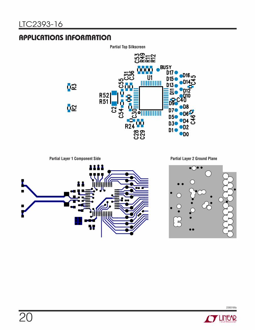
APPLICATIONS INFORMATIONBOARD LAYOUT
To obtain the best performance from the LTC2393-16, a printed circuit board (PCB) is recommended. Layout for the printed circuit board should ensure the digital and analog signal lines are separated as much as possible. In particular, care should be taken not to run any digital clocks or signals alongside analog signals or underneath the ADC.
Recommended Layout
The following is an example of a recommended PCB layout. A single solid ground plane is used. Bypass capacitors to the supplies are placed as close as possible to the supply pins. Low impedance common returns for these bypass capacitors are essential to the low noise operation of the ADC. The analog input traces are screened by ground. For more details and information refer to DC1500A, the evaluation kit for the LTC2393-16
Partial Schematic of Demoboard
BUSYD15D14D13D12
D11/SCLKD10/SDOUT
D9/SDIND8D7D6D5D4D3D2D1D0
BYTESWAPGND
BUSYD15D14D13D12D11/SCLKD10/SDOUTD9/SDIND8D7D6D5D4D3D2D1D0
29282726252423222116151413121110987
RD
30
CS
31
PD
33
RESET
REFOUT
3738
C361μF
3934
REFINREFSENSE
LTC2393-16
IN+
IN–
CNVST
CNVST
32
SER/PAR
4
GND
5
VCM
AVP/AVL AVP AVP AVP AVP
GND GND GND GND GND GND OGND
LTC2393-16
DVP OVP
18
3.3V
319
R241.0Ω
2
48 44 41 35 20 1 17239316 TA02
40454647
DVP/DVL
36
43
R2249Ω1%
R3249Ω1% 44
C5310μF
5V
C55OPT
OB/2C
6
C404.7μF
C290.1μF
C2810μF
C3010μF
C310.1μF
C54OPT
C22200pF1206 NPO
LTC2393-16
20239316fa
APPLICATIONS INFORMATIONPartial Top Silkscreen
Partial Layer 1 Component Side Partial Layer 2 Ground Plane

LTC2393-16
21239316fa
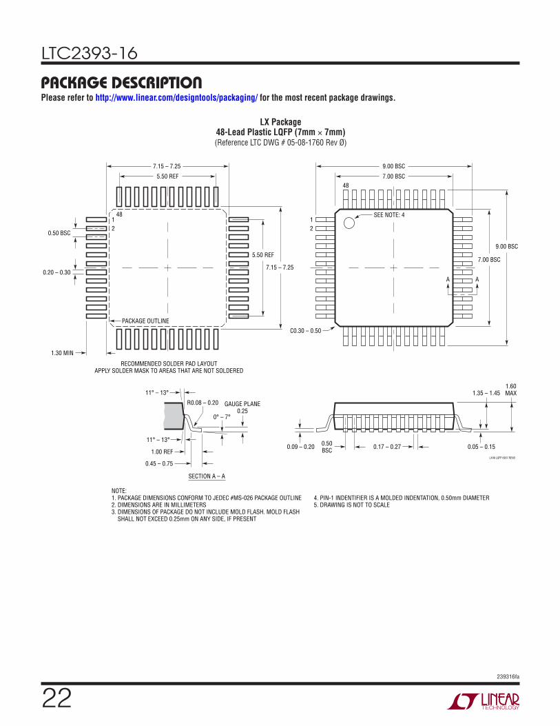
PACKAGE DESCRIPTIONPlease refer to http://www.linear.com/designtools/packaging/ for the most recent package drawings.
7.00 ±0.10(4 SIDES)
NOTE:1. DRAWING CONFORMS TO JEDEC PACKAGE OUTLINE MO-220 VARIATION (WKKD-2)2. DRAWING NOT TO SCALE 3. ALL DIMENSIONS ARE IN MILLIMETERS4. DIMENSIONS OF EXPOSED PAD ON BOTTOM OF PACKAGE DO NOT INCLUDE MOLD FLASH. MOLD FLASH, IF PRESENT, SHALL NOT EXCEED 0.20mm ON ANY SIDE, IF PRESENT5. EXPOSED PAD SHALL BE SOLDER PLATED6. SHADED AREA IS ONLY A REFERENCE FOR PIN 1 LOCATION ON THE TOP AND BOTTOM OF PACKAGE
PIN 1 TOP MARK(SEE NOTE 6)
PIN 1CHAMFER
C = 0.35
0.40 ±0.10
4847
1
2
BOTTOM VIEW—EXPOSED PAD
5.50 REF(4-SIDES)
0.75 ±0.05 R = 0.115TYP
0.25 ±0.05
0.50 BSC
0.200 REF
0.00 – 0.05
(UK48) QFN 0406 REV C
RECOMMENDED SOLDER PAD PITCH AND DIMENSIONSAPPLY SOLDER MASK TO AREAS THAT ARE NOT SOLDERED
0.70 ±0.05
5.50 REF(4 SIDES) 6.10 ±0.05 7.50 ±0.05
0.25 ±0.050.50 BSC
PACKAGE OUTLINE
5.15 ±0.10
5.15 ±0.10
5.15 ±0.05
5.15 ±0.05
R = 0.10TYP
UK Package48-Lead Plastic QFN (7mm 7mm)
(Reference LTC DWG # 05-08-1704 Rev C)
LTC2393-16
22239316fa
LX Package48-Lead Plastic LQFP (7mm × 7mm)(Reference LTC DWG # 05-08-1760 Rev Ø)
LX48 LQFP 0907 REVØ
0° – 7°
11° – 13°
0.45 – 0.75
1.00 REF
11° – 13°
9.00 BSC
A A
7.00 BSC
1
2
7.00 BSC
9.00 BSC
48
1.60MAX1.35 – 1.45
0.05 – 0.150.09 – 0.200.50BSC
0.17 – 0.27
GAUGE PLANE0.25
NOTE:1. PACKAGE DIMENSIONS CONFORM TO JEDEC #MS-026 PACKAGE OUTLINE2. DIMENSIONS ARE IN MILLIMETERS3. DIMENSIONS OF PACKAGE DO NOT INCLUDE MOLD FLASH. MOLD FLASH SHALL NOT EXCEED 0.25mm ON ANY SIDE, IF PRESENT
4. PIN-1 INDENTIFIER IS A MOLDED INDENTATION, 0.50mm DIAMETER5. DRAWING IS NOT TO SCALE
SEE NOTE: 4
C0.30 – 0.50
R0.08 – 0.20
7.15 – 7.25
5.50 REF
1
2
5.50 REF
7.15 – 7.25
48
PACKAGE OUTLINE
RECOMMENDED SOLDER PAD LAYOUTAPPLY SOLDER MASK TO AREAS THAT ARE NOT SOLDERED
SECTION A – A
0.50 BSC
0.20 – 0.30
1.30 MIN
PACKAGE DESCRIPTIONPlease refer to http://www.linear.com/designtools/packaging/ for the most recent package drawings.

LTC2393-16
23239316fa
Information furnished by Linear Technology Corporation is believed to be accurate and reliable. However, no responsibility is assumed for its use. Linear Technology Corporation makes no representa-tion that the interconnection of its circuits as described herein will not infringe on existing patent rights.
REVISION HISTORYREV DATE DESCRIPTION PAGE NUMBER
A 7/12 Increased TJMAX to 150°C on LQFP package
Increased SFDR specification under Dynamic Accuray to 108dB
Updated SNR, SINAD vs Input Frequency graph
Added condition for reading conversion result under Serial Modes
Updated data bit numbering on Figure 12
2
3
7
16
18

LTC2393-16
24239316fa
Linear Technology Corporation1630 McCarthy Blvd., Milpitas, CA 95035-7417 (408) 432-1900 ● FAX: (408) 434-0507 ● www.linear.com © LINEAR TECHNOLOGY CORPORATION 2010
LT 0712 REV A • PRINTED IN USA
RELATED PARTS
TYPICAL APPLICATION
PART NUMBER DESCRIPTION COMMENTS
LTC1411 14-Bit 2.5Msps Parallel ADC 5V Supply, 1-Channel, 80dB SNR, ±1.8V, ±1.27V, ±0.9V, ±0.64V Input Ranges, SSOP-36 Package
LTC1609 16-Bit 200ksps Serial ADC 5V Supply, 1-Channel, 87dB SNR, Resistor-Selectable Inputs: ±10V, ±5V, ±3.3V, 0V to 4V, 0V to 5V, 0V to 10V
LTC1864 16-Bit 250ksps Serial ADC 5V Supply, 1-Channel, 4.3mW, MSOP-8 Package
LTC1864L 16-Bit 150ksps Serial ADC 3V Supply, 1-Channel, 1.3mW, MSOP-8 Package
LTC1865 16-Bit 250ksps Serial ADC 5V Supply, 2-Channel, 4.3mW, MSOP-8 Package
LTC1865L 16-Bit 150ksps Serial ADC 3V Supply, 2-Channel, 1.3mW, MSOP-8 Package
LTC1867 16-Bit, 200ksps 8-Channel ADC 5V Supply, 6.5mW, SSOP-16 Package, Pin Compatible with LTC1863, LTC1867L
LTC2355-14/LTC2356-14 14-Bit, 3.5Msps Serial ADC 3.3V Supply, 1-Channel, 18mW, MSOP-10 Package
LTC2392-16 16-Bit, 500ksps Parallel/Serial ADC 5V Supply, Differential Input, 94dB SNR, ±4.096V Input Range, Pin Compatible with the LTC2393-16, LTC2391-16
LTC2391-16 16-Bit, 250ksps Parallel/Serial ADC 5V Supply, Differential Input, 94dB SNR, ±4.096V Input Range, Pin Compatible with the LTC2393-16, LTC2392-16
DACs
LTC2641 16-Bit Single Serial VOUT DACs ±1LSB INL, ±1LSB DNL, MSOP-8 Package, 0V to 5V Output
LTC2630 12-/10-/8-Bit Single VOUT DACs SC70 6-Pin Package, Internal Reference, ±1LSB INL (12 Bits)
References
LT1236 Precision Reference in SO-8 Package 5V, 10V; 0.05% Initial Accuracy (Max); 5ppm Tempco (Max)
LTC6655 0.25ppmP-P Noise, Low Drift Precision Reference 2.025% Initial Accuracy (Max), 2ppm Tempco (Max), 0.25ppmP-P Noise (0.1Hz to 10Hz) in MSOP-8 Package
Amplifiers
LT1469 Dual 90MHz, 22V/μs Dual Op Amps in 4mm × 4mm DFN-12 Package
125μV (Max) Input Offset Voltage, Low Distortion: –96.5dB at 100kHz, 10VP-P , Settling Time: 900ns
LT1806/LT1807 325MHz, Single/Dual Precision Op Amp in TSOT23-6 Package
Rail-to-Rail Input and Output, Low Distortion, –80dBc at 5MHz, Low Voltage Noise: 3.5nV/√Hz
LTC6200/LTC6200-5/ LTC6200-10
165MHz/800MHz/1.6GHz Op Amp with Unity Gain/AV = 5/AV = 10
Low Noise Voltage: 0.95nV/√Hz (100kHz), Low Distortion: –80dB at 1MHz, TSOT23-6 Package
LT6350 Low Noise Single-Ended-to-Differential ADC Driver Rail-to-Rail Input and Outputs, 240ns 0.01% Settling Time
+– +IN1
–IN1
V+
V–
OUT2
OUT1
SHDN
+IN2
VIN0V to 4V
5V
5V
0.1μF
0.1μF 0.1μF499Ω
2V –5V
LT6350
239316 TA03
+
–
249Ω
249Ω
2200pF
+
–AIN
–
AIN+
LTC2393-16
ADC Driver: Single-Ended Input to Differential Output