ltc4265 – ieee 802.3 at high power pd interface controller ... · ieee 802.3 at high power pd...
TRANSCRIPT

LTC4265
14265fb
For more information www.linear.com/LTC4265
Typical applicaTion
DescripTion
IEEE 802.3 at High Power PD Interface Controller with
2-Event Classification Recognition
The LTC®4265 is a 3rd generation Powered Device (PD) Interface controller intended for IEEE 802.3at high power Power-over-Ethernet (PoE) applications up to 25.5W. By supporting 1-event and 2-event classification signaling as defined by IEEE 802.3, the LTC4265 can be used in a wide range of product configurations. A 100V MOSFET isolates the DC/DC converter during detection and classification, and provides 100mA inrush current for a smooth power-up transition. The LTC4265 also includes complementary power good outputs, an on-board signature resistor, undervoltage/overvoltage lockout and comprehensive thermal protection. All Linear Technology PD solutions include a shutdown pin with signature corrupt to provide flexible auxiliary power options.
The LTC4265 PD interface controller can be used along with a variety of DC/DC converter products to provide a complete, cost effective power solution for high power PD applications.
The LTC4265 is available in the space-saving low profile (4mm × 3mm) DFN package and is drop-in compatible with the LTC4264.
Turn-On vs Time
L, LT, LTC, LTM, Linear Technology and the Linear logo are registered trademarks of Linear Technology Corporation. All other trademarks are the property of their respective owners.
FeaTures
applicaTions
n IEEE 802.3af/at Powered Device (PD) Controllern IEEE 802.3at 2-event Classification Signalingn Programmable Classification Currentn Flexible Auxiliary Power Support Using SHDN Pinn Rugged 100V Onboard MOSFET with 100mA Inrush
Current Limit.n Complementary Power Good Outputsn Onboard Signature Resistorn Comprehensive Thermal Protection n Undervoltage and Overvoltage Lockoutn 12-Lead, 4mm × 3mm DFN Package
n 802.11n Access Pointsn High Power VoIP Video Phonesn RFID Reader Systemsn PTZ Security Cameras and Surveillance Equipment
GND
RCLASS
SHDN
RCLASS
54V FROMDATA PAIR
54V FROMSPARE PAIR
0.1µF
PWRGD
PWRGD
LTC4265
T2PSE
V+
RUN
5µFMIN
3.3VTO LOGICRTN
SWITCHINGPOWERSUPPLY
VIN VOUT
4265 TA01a
+
–
+
~
~
+
–
~
~
+
–
TO LOGICTO AUX
GND – VIN50V/DIV
GND – VOUT50V/DIV
PWRGD – VOUT50V/DIV
IPD100mA/DIV
TIME25ms/DIV 4265 TA01b
CLOAD = 100µF
!

LTC4265
24265fb
For more information www.linear.com/LTC4265
pin conFiguraTionabsoluTe MaxiMuM raTings
GND Voltage ............................................ –0.3V to 100VVOUT Voltage ........................–0.3V to 100V (and ≤ GND)VOUT Pull-Up Current ..................................................1ASHDN ....................................................... –0.3V to 100VRCLASS, Voltage ............................................ –0.3V to 7VRCLASS Current .......................................................50mAPWRGD Voltage (Note 4) Low Impedance Source .....VOUT – 0.3V to VOUT +11V Pull-Up Current ....................................................5mAPWRGD, T2PSE Voltage ........................... –0.3V to 100VPWRGD, T2PSE Pull-Down Current .......................10mAJunction Temperature ........................................... 125°COperating Ambient Temperature Range LTC4265C ................................................ 0°C to 70°C LTC4265I.............................................. –40°C to 85°C
(Notes 1, 2, 3)
12
11
10
9
8
7
13
1
2
3
4
5
6
GND
NC
PWRGD
PWRGD
VOUT
VOUT
SHDN
T2PSE
RCLASS
NC
VIN
VIN
TOP VIEW
DE PACKAGE12-LEAD (4mm × 3mm) PLASTIC DFN
TJMAX = 125°C, θJA = 43°C/W EXPOSED PAD (PIN 13) TO BE TIED TO VIN AND SOLDERED TO PCB HEAT SINK
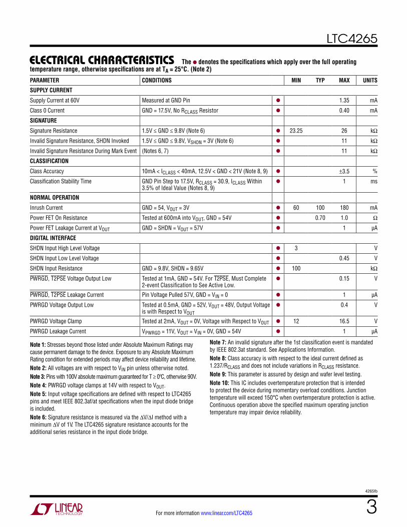
elecTrical characTerisTics The l denotes the specifications which apply over the full operating temperature range, otherwise specifications are at TA = 25°C. (Note 2)
PARAMETER CONDITIONS MIN TYP MAX UNITS
Operating Input Voltage Signature Range Classification Range Turn-On Voltage Undervoltage Lock Out Overvoltage Lock Out
At GND Pin (Note 5)
l
l
l
l
1.5
12.5
30.0
71
60 9.8 21
37.2
V V V V V V
ON/UVLO Hysteresis Window l 4.1 V
Signature/Class Hysteresis Window l 1.4 V
Reset Threshold State Machine Reset for 2-event Classification l 2.57 5.40 V
orDer inForMaTionLEAD FREE FINISH TAPE AND REEL PART MARKING* PACKAGE DESCRIPTION TEMPERATURE RANGE
LTC4265CDE#PBF LTC4265CDE#TRPBF 4265 12-Lead (4mm × 3mm) Plastic DFN 0°C to 70°C
LTC4265IDE#PBF LTC4265IDE#TRPBF 4265 12-Lead (4mm × 3mm) Plastic DFN –40°C to 85°C
Consult LTC Marketing for parts specified with wider operating temperature ranges. *The temperature grade is identified by a label on the shipping container. Consult LTC Marketing for information on non-standard lead based finish parts.For more information on lead free part marking, go to: http://www.linear.com/leadfree/ For more information on tape and reel specifications, go to: http://www.linear.com/tapeandreel/
LTC4265
34265fb
For more information www.linear.com/LTC4265
elecTrical characTerisTics
Note 1: Stresses beyond those listed under Absolute Maximum Ratings may cause permanent damage to the device. Exposure to any Absolute Maximum Rating condition for extended periods may affect device reliability and lifetime.Note 2: All voltages are with respect to VIN pin unless otherwise noted.Note 3: Pins with 100V absolute maximum guaranteed for T ≥ 0ºC, otherwise 90V.Note 4: PWRGD voltage clamps at 14V with respect to VOUT.Note 5: Input voltage specifications are defined with respect to LTC4265 pins and meet IEEE 802.3af/at specifications when the input diode bridge is included. Note 6: Signature resistance is measured via the ΔV/ΔI method with a minimum ΔV of 1V. The LTC4265 signature resistance accounts for the additional series resistance in the input diode bridge.
The l denotes the specifications which apply over the full operating temperature range, otherwise specifications are at TA = 25°C. (Note 2)
Note 7: An invalid signature after the 1st classification event is mandated by IEEE 802.3at standard. See Applications Information.Note 8: Class accuracy is with respect to the ideal current defined as 1.237/RCLASS and does not include variations in RCLASS resistance. Note 9: This parameter is assured by design and wafer level testing.Note 10: This IC includes overtemperature protection that is intended to protect the device during momentary overload conditions. Junction temperature will exceed 150°C when overtemperature protection is active. Continuous operation above the specified maximum operating junction temperature may impair device reliability.
PARAMETER CONDITIONS MIN TYP MAX UNITS
SUPPLY CURRENT
Supply Current at 60V Measured at GND Pin l 1.35 mA
Class 0 Current GND = 17.5V, No RCLASS Resistor l 0.40 mA
SIGNATURE
Signature Resistance 1.5V ≤ GND ≤ 9.8V (Note 6) l 23.25 26 kΩ
Invalid Signature Resistance, SHDN Invoked 1.5V ≤ GND ≤ 9.8V, VSHDN = 3V (Note 6) l 11 kΩ
Invalid Signature Resistance During Mark Event (Notes 6, 7) l 11 kΩ
CLASSIFICATION
Class Accuracy 10mA < ICLASS < 40mA, 12.5V < GND < 21V (Note 8, 9) l ±3.5 %
Classification Stability Time GND Pin Step to 17.5V, RCLASS = 30.9, ICLASS Within 3.5% of Ideal Value (Notes 8, 9)
l 1 ms
NORMAL OPERATION
Inrush Current GND = 54, VOUT = 3V l 60 100 180 mA
Power FET On Resistance Tested at 600mA into VOUT, GND = 54V l 0.70 1.0 Ω
Power FET Leakage Current at VOUT GND = SHDN = VOUT = 57V l 1 µA
DIGITAL INTERFACE
SHDN Input High Level Voltage l 3 V
SHDN Input Low Level Voltage l 0.45 V
SHDN Input Resistance GND = 9.8V, SHDN = 9.65V l 100 kΩ
PWRGD, T2PSE Voltage Output Low Tested at 1mA, GND = 54V. For T2PSE, Must Complete 2-event Classification to See Active Low.
l 0.15 V
PWRGD, T2PSE Leakage Current Pin Voltage Pulled 57V, GND = VIN = 0 l 1 µA
PWRGD Voltage Output Low Tested at 0.5mA, GND = 52V, VOUT = 48V, Output Voltage is with Respect to VOUT
l 0.4 V
PWRGD Voltage Clamp Tested at 2mA, VOUT = 0V, Voltage with Respect to VOUT l 12 16.5 V
PWRGD Leakage Current VPWRGD = 11V, VOUT = VIN = 0V, GND = 54V l 1 µA

LTC4265
44265fb
For more information www.linear.com/LTC4265
Typical perForMance characTerisTics
Input Current vs Input Voltage 25k Detection Range Input Current vs Input Voltage Input Current vs Input Voltage
GND VOLTAGE (V)0
0
INPU
T CU
RREN
T (m
A)
0.1
0.2
0.3
0.4
0.5
2 4 6 8
4265 G01
10
TA = 25°C
GND VOLTAGE (V)(RISING)
00
INPU
T CU
RREN
T (m
A)
10
20
30
40
50
10 20 30 40
4265 G02
50 60
TA = 25°C
CLASS 4
CLASS 3
CLASS 2
CLASS 1
CLASS 0
!
GND VOLTAGE (V)12
9.5
INPU
T CU
RREN
T (m
A)
10.5
14 16
4265 G03
10.0
18 20 22
11.0
85°C
–40°C
CLASS 1 OPERATION
!
Signature Resistance vs Input Voltage Class Operation vs Time On Resistance vs Temperature
GND VOLTAGE (V)
122
V1:V2:
SIGN
ATUR
E RE
SIST
ANCE
(kΩ
)
23
25
26
27
3 5
4265 G04
24
7 96 102 4 8
28RESISTANCE =
DIODES: HD01TA = 25°C
= ∆V∆I
V2 – V1I2 – I1
IEEE UPPER LIMIT
IEEE LOWER LIMITLTC4265 ONLY
!
LTC4265 + 2 DIODES
INPUTVOLTAGE
10V/DIV
CLASSCURRENT10mA/DIV
TIME (10µs/DIV) 4265 G05
TA = 25°C
!
JUNCTION TEMPERATURE (°C)–50
0.2
RESI
STAN
CE (Ω
)
0.4
0.6
0.8
1.0
–25 0 25 50
4265 G06
75 100

LTC4265
54265fb
For more information www.linear.com/LTC4265
Typical perForMance characTerisTics
PWRGD, T2PSE Output Low Voltage vs Current
Active High PWRGD Output Low Voltage vs Current Inrush Current vs Input Voltage
CURRENT (mA)0
V PW
RGD
(V)
V T2P
SE (V
)
0.4
0.6
8
4265 G07
0.2
02 4 6 10
0.8TA = 25°C
!
CURRENT (mA)0
0
PWRG
D (V
)0.4
1.0
0.5 1
4265 G08
0.2
0.8
0.6
1.5 2
TA = 25°CGND – VOUT = 4V
GND VOLTAGE (V)40
85
CURR
ENT
(mA)
115
45 50
4265 G09
55 60
90
100
105
110
95
90
100
105
110
95
pin FuncTionsSHDN (Pin 1): Shutdown Input. Use this pin for auxiliary power application. Drive SHDN high to disable LTC4265 operation and corrupt the signature resistance. If unused, tie SHDN to VIN.
T2PSE (Pin 2): Type-2 PSE Indicator, Open-Drain. Low impedance indicates the presence of a Type-2 PSE.
RCLASS (Pin 3): Class Select Input. Connect a resistor between RCLASS and VIN to set the classification load current. (See Table 2.)
NC (Pin 4, 11): No Connect.
VIN (Pins 5, 6): Input Voltage, Negative Rail. Pins 5 and 6 must be electrically tied together at the package.
VOUT (Pins 7, 8): Output Voltage Negative Rail. Connects VOUT to VIN through an internal power MOSFET. Pins 7 and 8 must be electrically tied together at the package.
PWRGD (Pin 9): Power Good Output, Open Collector. High impedance signals power-up completion. PWRGD is referenced to VOUT and features a 14V clamp.
PWRGD (Pin 10): Complementary Power Good Output, Open-Drain. Low impedance signals power up completion. PWRGD is referenced to VIN.
GND (Pin 12): Input Voltage, Positive Rail. This pin is connected to the PD positive rail.
Exposed Pad (Pin 13): Tie to VIN and PCB heat sink.

LTC4265
64265fb
For more information www.linear.com/LTC4265
block DiagraM
4265 BD
BOLD LINE INDICATES HIGH CURRENT PATH
12
T2PSE 2
RCLASS 3
NC 4
SHDN
PWRGD
GND
11 NC
1
10
PWRGD9
VOUT8
VOUT7
CONTROLCIRCUITS
CLASSIFICATIONCURRENT LOAD
REF
–
+
25k 14k
EXPOSED PAD 13
VIN 6
VIN 5
EN

LTC4265
74265fb
For more information www.linear.com/LTC4265
applicaTions inForMaTionOVERVIEW
Power over Ethernet (PoE) continues to gain popularity as more products are taking advantage of having DC power and high speed data available from a single RJ45 connector. As PoE continues to grow in the marketplace, Powered Device (PD) equipment vendors are running into the 12.95W power limit established by the IEEE 802.3af standard.
The IEE802.3at standard establishes a higher power allocation for Power-over-Ethernet while maintaining backwards compatibility with the existing IEEE802.3af systems. Power Sourcing Equipments (PSE) and Powered Devices are distinguished as Type-1 complying with the IEEE 802.3af power levels, or Type-2 complying with the IEEE 802.3at power levels. The maximum available power of a Type-2 PD is 25.5W.
The IEEE802.3at standard also establishes a new method of acquiring power classification from a PD and communi-cating the presence of a Type-2 PSE. A Type-2 PSE has the option of acquiring PD power classification by performing 2-event classification (Layer 1) or by communicating with the PD over the data line (Layer 2). In turn, a Type-2 PD must be able to recognize both layers of communications and identify a Type-2 PSE.
The LTC4265 is specifically designed to support the front end of a PD that must operate under the IEEE802.3at standard. In particular, the LTC4265 provides the T2PSE indicator bit which recognizes 2-event classification. This indicator bit may be used to alert the LTC4265 output load that a Type-2 PSE is present. With an internal signature resistor, classification circuitry, inrush control, and ther-mal shutdown, the LTC4265 is a complete PD Interface solution capable of supporting in the next generation PD applications.
MODES OF OPERATION
The LTC4265 has several modes of operation depending on the input voltage applied between the GND and VIN pins. Figure 1 presents an illustration of voltage and current waveforms the LTC4265 may encounter with the various modes of operation summarized in Table 1.
DETECTION V1
CLASSIFICATION
ONUVLO
UVLO
POWERBAD
UVLOON
τ = RLOAD C1
PWRGD TRACKSVIN
DETECTION V2
50
TIME
40
30
GND
– V I
N (V
)
20
10
50
40
30
20
10TIME
GND
– V O
UT (V
)
–10
TIME
–20
–30
GND
– PW
RGD
(V)
PWRG
D –
V OUT
(V)
–40
–50
20
10
PD C
URRE
NT
INRUSH
dVdt
INRUSHC1
=
POWERBAD
PWRGDTRACKS
GND
PWRGDTRACKS
GND
POWERBAD
POWERBAD
TIME
TIME
POWERGOOD
POWERGOOD
DETECTION I1
CLASSIFICATION
DETECTION I2
LOAD, ILOAD
4265 F01
ICLASS DEPENDENT ON RCLASS SELECTION
INRUSH = 100mA
I1 = V1 – 2 DIODE DROPS25kΩ
ILOAD = VIN
RLOAD
I2 = V2 – 2 DIODE DROPS25kΩ
GNDPSE
IIN RLOAD
RCLASSVOUTC1
GND
RCLASS
PWRGD
PWRGD
LTC4265
VOUTVIN
IN DETECTIONRANGE
Figure 1. Output Voltage, PWRGD, PWRGD and PD Current as a Function of Input Voltage

LTC4265
84265fb
For more information www.linear.com/LTC4265
applicaTions inForMaTionThese modes satisfy the requirements defined in the IEEE 802.3af/at specification.
Table 1. LTC4265 Modes of Operation as a Function of Input VoltageGND (V) LTC4265 MODES OF OPERATION
0V to 1.4V Inactive (Reset After 1st Classification Event)
1.5V to 9.8V (5.4V to 9.8V)
25k Signature Resistor Detection Before 1st Classification Event (Mark, 11k Signature Corrupt After 1st Classification Event)
12.5V to ON/UVLO* Classification Load Current Active
ON/UVLO* to 60V Inrush and Power Applied To PD Load
>71V Overvoltage Lockout, 4265 Operations are Disabled
*ON/UVLO includes hysteresis. Rising input threshold, 37.2V Max. Falling input threshold, 30V Min.
INPUT DIODE BRIDGE
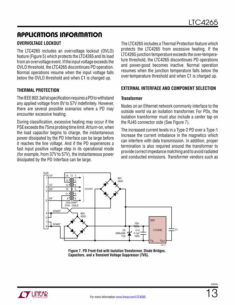
In the IEEE 802.3af/at standard, the modes of operation reference the input voltage at the PD’s RJ45 connector. Since the PD must handle power received in either polarity from either the data or the spare pair, input diode bridges BR1 and BR2 are connected between the RJ45 connector and the LTC4265 (Figure 2).
RX–6
RX+3
TX–2
TX+RJ45
T1
POWEREDDEVICE (PD)
INPUT
4265 F02
1
7
8
5
4
SPARE–
SPARE+
TO PHY
BR2
0.1µF100V
BR1
GND
D3LTC4265
VIN
Figure 2. PD Front End Using Diode Bridges on Main and Spare Inputs
The input diode bridge introduces a voltage drop that affects the range for each mode of operation. The LTC4265 compensates for these voltage drops so that a PD built with the LTC4265 meets the IEEE 802.3af/at-established voltage ranges. Note that the Electrical Specifications reference with respect to the LTC4265 package pins.
DETECTION
During detection, the PSE looks for a 25k signature resistor which identifies the device as a PD. The PSE will apply two voltages in the range of 2.8V to 10V and measures the corresponding currents. Figure 1 shows the detection voltages V1 and V2 and the corresponding PD current. The PSE calculates the signature resistance using the ΔV/ΔI measurement technique.
The LTC4265 presents its precision, temperature-compen-sated 25k resistor between the GND and VIN pins, alerting the PSE that a PD is present and requests power to be applied. The LTC4265 signature resistor also compensates for the additional series resistance introduced by the input diode bridge. Thus a PD built with the LTC4265 conforms to the IEEE 802.3af/at detection specifications.

LTC4265
94265fb
For more information www.linear.com/LTC4265
applicaTions inForMaTionSIGNATURE CORRUPT OPTION
In some designs that include an auxiliary power option, it is necessary to prevent a PD from being detected by a PSE. The LTC4265 signature resistance can be corrupted with the SHDN pin (Figure 3). Taking the SHDN pin high will reduce the signature resistor below 11k which is an invalid signature per the IEEE 802.3af/at specification, and alerts the PSE not to apply power. Invoking the SHDN pin also ceases operation for classification and disconnects the LTC4265 load from the PD input. If this feature is not used, connect SHDN to VIN.
During classification probing, the PSE presents a fixed voltage between 15.5V and 20.5V to the PD (Figure 2). The LTC4265 asserts a load current representing the PD power classification. The classification load current is programmed with a resistor RCLASS that is chosen from Table 2.
Table 2. Summary of Power Classifications and LTC4265 RCLASS Resistor SelectionCLASS USAGE MAXIMUM
AVERAGE POWER LEVELS AT INPUT
OF PD (W)
NOMINAL CLASSIFICATION LOAD CURRENT
(mA)
LTC4265 RCLASS
RESISTOR (Ω, 1%)
0 Default 0.44 to 13.0 < 0.4 Open
1 Optional 0.44 to 3.84 10.5 124
2 Optional 3.84 to 6.49 18.5 69.8
3 Optional 6.49 to 13.0 28 45.3
4 Optional 13.0 to 25.5 40 30.9
2-EVENT CLASSIFICATION AND THE T2PSE PIN
A Type-2 PSE may declare the availability of high power by performing 2-event classification (Layer 1) or by commu-nicating over the high speed data line (Layer 2). A Type-2 PD must recognize both layers of communication. Since Layer 2 communications takes place directly between the PSE and the LTC4265 load, the LTC4265 concerns itself only with recognizing 2-event classification.
Figure 3. 25k Signature Resistor with Disable
GND
VIN
SHDN
LTC4265
TO AUX
4265 F03
25k SIGNATURERESISTOR14kTO
PSE
CLASSIFICATION
Classification provides a method for more efficient power allocation by allowing the PSE to identify a PD power clas-sification. Class 0 is included in the IEEE specification for PDs that don’t support classification. Class 1-3 partitions PDs into 3 distinct power ranges. Class 4 includes the new power range under IEEE802.3at (See Table 2).

LTC4265
104265fb
For more information www.linear.com/LTC4265
applicaTions inForMaTionIn 2-event classification, a Type-2 PSE probes for power classification twice. Figure 4 presents an example of a 2-event classification. The 1st classification event occurs when the PSE presents an input voltage between 14.5V to 20.5V and the LTC4265 presents a class 4 load current. The PSE then drops the input voltage into the mark voltage range of 6.9V to 10V, signaling the 1st mark event. The PD in the mark voltage range presents a load current between 0.25mA to 4mA.
The PSE repeats this sequence, signaling the 2nd Clas-sification and 2nd mark event occurrence. This alerts the LTC4265 that a Type-2 PSE is present. The Type-2 PSE then applies power to the PD and the LTC4265 charges up the reservoir capacitor C1 with a controlled inrush current. When C1 is fully charged, and the LTC4265 declares power good, the T2PSE pin presents an active low signal, or low impedance output with respect to VIN. The T2PSE output becomes inactive when the LTC4265 input voltage falls outside the normal operating range.
SIGNATURE CORRUPT DURING MARK
As a member of the IEEE802.3at working group, Linear notes that it is possible for a Type-2 PD to receive a false indication of a 2-event classification if a PSE port is pre-charged to a voltage above the detection voltage range before the first detection cycle. The IEEE working group modified the standard to prevent this possibility by requiring a Type-2 PD to corrupt the signature resistance during the mark event, alerting the PSE not to apply power. The LTC4265 conforms to this standard by internally corrupting the signature resistance. This also discharges the port before the PSE begins the next detection cycle.
DETECTION V1
ONUVLO
UVLO UVLOON
τ = RLOAD C1
TRACKSVIN
DETECTION V2
TIME
PD C
URRE
NT
50
40
30
GND
(V)
20
10
40mA
50
40
30
20
10
TIME
GND
– V O
UT (V
)
–10TIME
–20
–30
GND
– T2
PSE
(V)
–40
–50
dVdt
INRUSHC1
=
4265 F04
INRUSH = 100mA RCLASS = 30.9Ω
ILOAD = VIN
RLOAD
GNDPSE
IIN RLOAD
RCLASSVOUTC1
GND
RCLASS
T2PSE
LTC4265
VOUTVIN
!!
1st CLASS
1st MARK 2nd MARK
DETECTION V1DETECTION V2
1st MARK 2nd MARK
2nd CLASS
1st CLASS2nd CLASS
LOAD, ILOAD
INRUSH
Figure 4. VOUT, T2PSE, and PD Current as a Result of 2-event Classification

LTC4265
114265fb
For more information www.linear.com/LTC4265
applicaTions inForMaTionPD STABILITY DURING CLASSIFICATION
Classification presents a challenging stability problem due to the wide range of possible classification load current. The onset of the classification load current introduces a voltage drop across the cable and increases the forward voltage of the input diode bridge. This may cause the PD to oscillate between detection and classification with the onset and removal of the classification load current.
The LTC4265 prevents this oscillation by introducing a voltage hysteresis window between the detection and clas-sification ranges. The hysteresis window accommodates the voltage changes a PD encounters at the onset of the classification load current, thus providing a trouble-free transition between detection and classification modes.
The LTC4265 also maintains a positive I-V slope throughout the classification ranges up to the ON voltage. In the event a PSE overshoots beyond the classification voltage range, the available load current aids in returning the PD back into the classification voltage range. (The PD input may otherwise be “trapped” by a reverse-biased diode bridge and the voltage held by the 0.1μF capacitor.)
INRUSH CURRENT
Once the PSE detects and optionally classifies the PD, the PSE then applies powers on the PD. When the LTC4265 input voltage rises above the ON voltage threshold, LTC4265 connects VOUT to VIN through the internal power MOSFET.
To control the power-on surge currents in the system, the LTC4265 provides a fixed inrush current, allowing C1 to ramp up to the line voltage in a controlled manner.
The LTC4265 keeps the PD inrush current below the PSE current limit to provide a well-controlled power-up characteristic that is independent of the PSE behavior.
Figure 5. LTC4265 Undervoltage and Overvoltage Lockout
GNDC1
5µFMIN
VIN VOUT
LTC4265
4265 F05
TOPSE
UNDERVOLTAGEOVERVOLTAGE
LOCKOUTCIRCUIT
PDLOAD
CURRENT-LIMITEDTURN ON
+
INPUT LTC4265VOLTAGE POWER MOSFET0V TO ON* OFF>ON* ON<UVLO* OFF>OVLO OFF*INCLUDES ON-UVLO HYSTERESISON THRESHOLD ≅ 36.1VUVLO THRESHOLD ≅ 30.7VOVLO THRESHOLD ≅ 71.0V
This ensures a PD using the LTC4265 interoperability with any PSE.
UNDERVOLTAGE LOCKOUT
The IEEE 802.3af/at specification for the PD dictates a maximum turn-on voltage of 42V and a minimum turn-off voltage of 30V. This specification provides an adequate voltage to begin PD operation, and to discontinue PD operation when the input voltage is too low. In addition, this specification allows PD designs to incorporate an on-off hysteresis window to prevent start-up oscillations.
The LTC4265 features an ON-undervoltage lockout (UVLO) hysteresis window (See Figure 5) that conforms with the IEEE 802.3af/at specifications and accommodates the voltage drop in the cable and input diode bridge at the onset of the inrush current.

LTC4265
124265fb
For more information www.linear.com/LTC4265
applicaTions inForMaTionOnce C1 is fully charged, the LTC4265 turns on is internal MOSFET and passes power to the PD load. The LTC4265 continues to power the PD load as long as the input voltage does not fall below the UVLO threshold. When the LTC4265 input voltage falls below the UVLO threshold, the PD load is disconnected, and classification mode resumes. C1 discharges through the LTC4265 circuitry.
COMPLEMENTARY POWERGOOD
When LTC4265 fully charges the load capacitor (C1), power good is declared and the LTC4265 load can safely begin operation. The LTC4265 provides complementary power good signals that remain active during normal operation and are de-asserted when the input voltage falls below the UVLO threshold, when the input voltage exceeds the over-voltage lockout (OVLO) threshold, or in the event of a thermal shutdown. See Figure 6.
The PWRGD pin features an open collector output refer-enced to VOUT which can interface directly with the “Run” pin of a DC/DC converter product. When power good is declared and active, the PWRGD pin is high impedance with respect to VOUT. An internal 14V clamp protects the DC/DC converter from an excessive voltage.
The active low PWRGD pin connects to an internal, open drain MOSFET referenced to VIN and can interface directly to the shutdown pin of a DC/DC converter product. When power good is declared and active, the PWRGD pin is low impedance with respect to VIN.
Figure 6. LTC4265 Power Good Functional and State Diagram
4265 F06
BOLD LINE INDICATES HIGH CURRENT PATH
PWRGD
POWERNOT
GOOD
INRUSH COMPLETEON < GND < OVLO
AND NOT IN THERMAL SHUTDOWN
GND < UVLOGND > OVLO
OR THERMAL SHUTDOWN
POWERGOOD
9
PWRGDLTC4265
10
VOUT8
VOUT7VIN 6
VIN
OVLOON
UVLOTSD
5
CONTROLCIRCUIT
PWRGD PIN WHEN SHDN IS INVOKED
In PD applications where an auxiliary power supply invokes the SHDN feature, the PWRGD pin becomes high imped-ance. This prevents the PWRGD pin that is connected to the “Run” pin of the DC/DC converter from interfering with the DC/DC converter operations when powered by an auxiliary power supply.
LTC4265
134265fb
For more information www.linear.com/LTC4265
applicaTions inForMaTionOVERVOLTAGE LOCKOUT
The LTC4265 includes an overvoltage lockout (OVLO) feature (Figure 5) which protects the LTC4265 and its load from an overvoltage event. If the input voltage exceeds the OVLO threshold, the LTC4265 discontinues PD operation. Normal operations resume when the input voltage falls below the OVLO threshold and when C1 is charged up.
THERMAL PROTECTION
The IEEE 802.3af/at specification requires a PD to withstand any applied voltage from 0V to 57V indefinitely. However, there are several possible scenarios where a PD may encounter excessive heating.
During classification, excessive heating may occur if the PSE exceeds the 75ms probing time limit. At turn-on, when the load capacitor begins to charge, the instantaneous power dissipated by the PD Interface can be large before it reaches the line voltage. And if the PD experiences a fast input positive voltage step in its operational mode (for example, from 37V to 57V), the instantaneous power dissipated by the PD Interface can be large.
14
13
12
1
2
3
RX–6
RX+3
TX–2
TX+RJ45
T1
COILCRAFTETHI - 230LD
4265 F07
1
7
8
5
4
10
9
11
5
6
4
D3SMAJ58A
TVS
BR1HD01
BR2HD01
TO PHY
GND
LTC4265 C1
VIN VOUT
SPARE–
SPARE+
C140.1µF100V
10Ω
Figure 7. PD Front-End with Isolation Transformer, Diode Bridges, Capacitors, and a Transient Voltage Suppressor (TVS).
The LTC4265 includes a Thermal Protection feature which protects the LTC4265 from excessive heating. If the LTC4265 junction temperature exceeds the over-tempera-ture threshold, the LTC4265 discontinues PD operations and power-good becomes inactive. Normal operation resumes when the junction temperature falls below the over-temperature threshold and when C1 is charged up.
EXTERNAL INTERFACE AND COMPONENT SELECTION
Transformer
Nodes on an Ethernet network commonly interface to the outside world via an isolation transformer. For PDs, the isolation transformer must also include a center tap on the RJ45 connector side (See Figure 7).
The increased current levels in a Type-2 PD over a Type-1 increase the current imbalance in the magnetics which can interfere with data transmission. In addition, proper termination is also required around the transformer to provide correct impedance matching and to avoid radiated and conducted emissions. Transformer vendors such as

LTC4265
144265fb
For more information www.linear.com/LTC4265
applicaTions inForMaTionBel Fuse, Coilcraft, Halo, Pulse, and Tyco (Table 4) can assist in selecting an appropriate isolation transformer and proper termination methods.
Table 4. Power-over-Ethernet Transformer VendorsVENDOR CONTACT INFORMATION
Bel Fuse Inc. 206 Van Vorst Street Jersey City, NJ 07302 Tel: 201-432-0463 www.belfuse.com
Coilcraft Inc. 1102 Silver Lake Road Gary, IL 60013 Tel: 847-639-6400 www.coilcraft.com
Halo Electronics 1861 Landings Drive Mountain View, CA 94043 Tel: 650-903-3800 www.haloelectronics.com
PCA Electronics 16799 Shoenborn Street North Hills, CA 91343 Tel: 818-892-0761 www.pca.com
Pulse Engineering 12220 World Trade DriveSan Diego, CA 92128 Tel: 858-674-8100 www.pulseeng.com
Tyco Electronics 308 Constitution Drive Menlo Park, CA 94025-1164 Tel: 800-227-7040 www.circuitprotection.com
Input Diode Bridge
Figure 2 shows how two diode bridges are typically con-nected in a PD application. One bridge is dedicated to the data pair while the other bridge is dedicated to the spare pair. The LTC4265 supports the use of either silicon or Schottky input diode bridges. However, there are tradeoffs in the choice of diode bridges.
An input diode bridge must exceed the maximum current the PD application will encounter at the temperature the PD will operate. Diode bridge vendors typically call out the operating current at room temperature, but derate the maximum current with increasing temperature. Consult the diode bridge vendors for the operating current der-ating curve.
A silicon diode bridge can consume over 4% of the available power in some PD applications. Using Schottky diodes can help reduce the power loss with a lower forward voltage.
A Schottky bridge may not be suitable for some high temperature PD application. The leakage current has a voltage dependency that can reduce the perceived signature resistance. In addition, the IEEE 802.3af/at specification mandates the leakage back-feeding through the unused bridge cannot generate more than 2.8V across a 100k resistor when a PD is powered with 57V.
Sharing Input Diode Bridges
At higher temperatures, a PD design may be forced to consider larger bridges in a bigger package because the maximum operating current for the input diode bridge is drastically de-rated. The larger package may not be acceptable in some space-limited environments.
One solution to consider is to reconnect the diode bridges so that only one of the four diodes conducts current in each package. This configuration extends the maximum operating current while maintaining a smaller package profiles. Figure 7 shows how to reconnect the two diode bridges. Consult the diode bridge vendors for the de-rating curve when only one of four diodes is in operation.
LTC4265
154265fb
For more information www.linear.com/LTC4265
applicaTions inForMaTionInput Capacitor
The IEEE 802.3af/at standard includes an impedance requirement in order to implement the AC disconnect function. A 0.1µF capacitor (C14 in Figure 7) is used to meet this AC impedance requirement.
Input Series Resistance
Linear Technology has seen the customer community cable discharge requirements increase by nearly 500,000 times the original test levels. The PD must survive and operate reliably not only when an initially charged cable connects and dissipates the energy through the PD front end, but also when the electrical power system grounds are subject to very high energy events (e.g. lightning strikes).
In these high energy events, adding 10Ω series resistance into the VPORTP pin greatly improves the robustness of the LTC4265 based PD. (See Figure 7.) The TVS limits the voltage across the port while the 10Ω and 0.1µF ca-pacitance reduces the edge rate the LT4265 encounters across its pin. The added 10Ω series resistance does not operationally affect the LTC4265 PD Interface nor does it affect its compliance with the IEEE 802.3 standard.
Transient Voltage Suppressor
The LTC4265 specifies an absolute maximum voltage of 100V and is designed to tolerate brief overvoltage events. However, the pins that interface to the outside world can routinely see excessive peak voltages. To protect the LTC4265, install a transient voltage suppressor (D3) be-tween the input diode bridge and the LTC4265 as shown in Figure 7.
An SMAJ58A is recommended for typical PD applications. However, an SMBJ58A may be preferred in applications where the PD front-end must absorb higher energy dis-charge events.
Classification Resistor (RCLASS)
The RCLASS resistor sets the classification load current, corresponding to the PD power classification. Select the value of RCLASS from Table 2 and connect the resistor between the RCLASS and VIN pins as shown in Figure 4, or
float the RCLASS pin if the classification load current is not required. The resistor tolerance must be 1% or better to avoid degrading the overall accuracy of the classification circuit.
Load Capacitor
The IEEE 802.3af/at specification requires that the PD maintains a minimum load capacitance of 5μF and does not specify a maximum load capacitor. However, if the load capacitor is too large, there may be a problem with inadvertent power shutdown by the PSE.
This occurs when the PSE voltage drops quickly. The input diode bridge reverses bias, and the PD load momentarily powers off the load capacitor. If the PD does not draw power within the PSE’s 300ms disconnection delay, the PSE may remove power from the PD. Thus, it is necessary to evaluate the load current and capacitance to ensure that an inadvertent shutdown cannot occur.
The load capacitor can store significant energy when fully charged. The PD design must ensure that this energy is not inadvertently dissipated in the LTC4265. For example, if the GND pin shorts to VIN while the capacitor is charged, current will flow through the parasitic body diode of the internal MOSFET and may cause permanent damage to the LTC4265.
Power Good Interface
The LTC4265 provides complementary power good sig-nals to simplify the DC/DC converter interface. Using the power good signal to delay converter operation until the load capacitor is fully charged is highly recommended to ensure trouble free start up.
Figure 8 presents examples of power good interface cir-cuits. The active high PWRGD pin has an open collector transistor referenced to VOUT while the active low PWRGD pin has a high voltage, open-drain MOSFET referenced to VIN. The designer can choose either signal to enable the DC/DC converter. When using PWRGD, diode D9 and resistor RS protects the converter shutdown pin from excessive reverse voltage.

LTC4265
164265fb
For more information www.linear.com/LTC4265
Figure 9. T2PSE Interface Examples
4265 F09
OPTION 1: SERIES CONFIGURATION FOR ACTIVE LOW/LOW IMPEDANCE OUTPUT
–54V
TOPSE
RP
TO PD LOAD
GND
LTC4265
VIN T2PSE
V+
OPTION 2: SHUNT CONFIGURATION FOR ACTIVE HIGH/OPEN COLLECTOR OUTPUT
–54V
TOPSE
RP
TO PD LOAD
GND
LTC4265
VIN
T2PSE
V+
applicaTions inForMaTion
Figure 8. Power Good Interface Examples
GND
RS10k
R10100k
PWRGD
D9MMBD4148
Q1FMMT2222
–54V4265 F08
TOPSE
LTC4265
ACTIVE-LOW ENABLE
VIN VOUT
V+
DC/DCCONV.
GND
RS10k
R9100k
PWRGDD9
5.1VMMBZ5231B
–54V
TOPSE
LTC4265
ACTIVE-LOW ENABLE
VIN VOUT
DC/DCCONV.
–54V
TOPSE
ACTIVE-HIGH ENABLE
DC/DCCONV.
RUN
SHDN
GND
PWRGD
LTC4265
VIN VOUT
Figure 9 shows two interface options using the T2PSE pin and the opto-isolator. The T2PSE pin is active low and connects to an opt-isolater to communicate across the DC/DC converter isolation barrier. The pull up resistor RP is sized according to the requirements of the opto-isolator operating current, the pull-down capability of the T2PSE pin, and the choice of V+. V+ for example can come from the PoE supply rail (which the LTC4265 GND is tied to), or from the voltage source that supplies power to the DC/DC converter. Option 1 has the advantage of not drawing power unless T2PSE is declared active.
T2PSE Interface
When a 2-event Classification sequence successfully completes, the LTC4265 recognizes this sequence, and provides an indicator bit, declaring the presence of a Type-2 PSE. The open drain output provides the option to use this signal to communicate to the LTC4265 load, or to leave the pin unconnected.

LTC4265
174265fb
For more information www.linear.com/LTC4265
applicaTions inForMaTionShutdown Interface
To corrupt the signature resistance, the SHDN pin can be driven high with respect to VIN or connected to GND. If unused, connect SHDN directly to VIN.
Exposed Pad
The LTC4265 uses a thermally enhanced DFN12 package that includes an Exposed Pad. The exposed pad must be electrically connected to VIN and must connect to a printed circuit board heat sink.
Auxiliary Power Source
In some applications, it is desirable to power the PD from an auxiliary power source such as a wall adapter.
Auxiliary power can be injected into an LTC4265-based PD at the input of the LTC4265, the output of the LTC4265, or even the output of the DC/DC converter. In addition, some PD application may desire auxiliary supply dominance or may be configured for PoE dominance. Furthermore, PD
applications may also opt for a seamless transition — that is, without power disruption — between PoE and auxiliary power.
The most common auxiliary power option injects power between the LTC4265 and the DC/DC converter. Figure 10 presents an example of this application.
In this example, the auxiliary port injects 48V onto the line via diode D1. The components surrounding the SHDN pin are selected so that the LTC4265 disconnects power to the output when the auxiliary supply reaches 36V.
This configuration is an auxiliary-dominant configuration. That is, the auxiliary power source supplies the power even if PoE power is already present. This configuration also provides a seamless transition from PoE to auxiliary power when auxiliary power is applied, however, the removal of auxiliary power to PoE power is not seamless.
Contact Linear Technology applications support for detail information on implementing a custom auxiliary power supply.
Figure 10. Auxiliary Power Dominant PD Interface
T1
4265 F10
TVS
TO PHY
36V100k
10k
10k
D1
BR1
+
–
BR2
+
–
0.1µF100V C1
GND
LTC4265
VIN
SHDN
VOUT
+
–
ISOLATEDWALL
TRANSFORMER
PDLOADRX–
6
RX+3
TX–2
TX+RJ45
1
7
8
5
4
SPARE–
SPARE+
LTC4265
184265fb
For more information www.linear.com/LTC4265
applicaTions inForMaTionIEEE 802.3at SYSTEM POWER-UP REQUIREMENT
Under the IEEE 802.3at standard, a PD must operate under 13.0 Watts as a Type 1 PD until it recognizes a Type-2 PSE. Initializing PD operation in 13.0-Watt mode eliminates interoperability issue in case a Type-2 PD is connects to a Type-1 PSE. Once the PD recognizes a Type-2 PSE, the IEEE 802.3at standard requires the PD to wait 80ms in 13.0W operation before 25.5W operation can commence.
MAINTAIN POWER SIGNATURE
In an IEEE 802.3af/at system, the PSE uses the maintain power signature (MPS) to determine if a PD continues to require power. The MPS requires the PD to periodically draw at least 10mA and also have an AC impedance less than 26.25k in parallel with 0.05μF. If one of these condi-tions is not met, the PSE may disconnect power to the PD.
LAYOUT CONSIDERATION FOR THE LTC4265
The LTC4265 is relatively immune to layout problems. Here are some recommendations.
Avoid excessive parasitic capacitance on the RCLASS pin and place resistor RCLASS close to the LTC4265.
Connect the LTC4265 exposed pad to a PC board heat sink. Make the heat sink as large as possible.
Place the input capacitor and transient voltage suppres-sor (C14 and D3 in Figure 7) as close to the LTC4265 as possible.
If using the SHDN pin for auxiliary power application, separate the SHDN pin from other high voltage connec-tions, like GND and VOUT, to avoid leakage and capacitive coupling shutting down the LTC4265.

LTC4265
194265fb
For more information www.linear.com/LTC4265
100k
12k
••
••
25m
Ω
FDS2
582
14k
3.01
k20Ω
30k
15µF
16V
29.4
k38
3k
30.9
Ω
BAS2
1
1.8k
38.3
k10
k
51k
1nF
10k
20k
15Ω
15Ω
150Ω
PE-6
8386
BAT5
4
100Ω
33pF
10µF
100V
0.1µ
F10
0VSM
AJ58
A
B110
0
10Ω
B110
0 ×
8 PL
CS1µ
F10
0V
0.1µ
F
4.7n
F
2.2n
F
MM
BT39
06M
MBT
3904
1µF
1µF
16V
PA24
67NL
4265
TA0
2
t ON
SYNC
PGDL
Y
UVLO
SENS
E– V C
SENS
E+
R CM
PEN
DLY
OSC
SFST
LT38
25
GND
SG
FB
V CC
SGSG
PG
C CM
P
GND
R CLA
SS
SHDN
LTC4
265
T2PS
E
V IN
V OUT
4.7µ
H
–54V
FRO
MDA
TA P
AIR
–54V
FRO
MSP
ARE
PAIR
47pF
•10
µF16
V
0.33
µH12
V2A
47µF
16V
FDS3
572
+
GND
45
18
GND LTV3
57TA
T2P
(TO
MIC
ROCO
NTRO
LLER
)
2.2n
F2k
V
470p
F2k
V
+
High
Effi
cien
cy 1
2V Is
olat
ed P
ower
Sup
ply
(Con
tact
LTC
for 3
.3V
and
5V P
ower
Sup
ply
Appl
icat
ions
)
applicaTions inForMaTion
LOAD
CUR
RENT
(A)
0.2
0.4
EFFICIENCY (%)
8589 87
2.0
4265
TA0
2a
8183 7779
0.6
0.8
1.2
1.0
1.6
1.8
1.4
93 91
57V
48V
EXCL
UDIN
G BR
IDGE
S42
V
LOAD
CUR
RENT
(A)
0.2
OUTPUT (V)
12.0
12.1
12.2
12.3
2.0
4265
TA0
2b
11.8
11.9
11.6
11.7
0.6
0.8
0.4
1.2
1.0
1.6
1.8
1.4
12.4
57V
48V
42V
Effic
ienc
y vs
Loa
d Cu
rren
tOu
tput
Reg
ulat
ion
vs L
oad
Curr
ent

LTC4265
204265fb
For more information www.linear.com/LTC4265
package DescripTionDE/UE Package
12-Lead Plastic DFN (4mm × 3mm)(Reference LTC DWG # 05-08-1695 Rev D)
4.00 ±0.10(2 SIDES)
3.00 ±0.10(2 SIDES)
NOTE:1. DRAWING PROPOSED TO BE A VARIATION OF VERSION (WGED) IN JEDEC PACKAGE OUTLINE M0-2292. DRAWING NOT TO SCALE3. ALL DIMENSIONS ARE IN MILLIMETERS4. DIMENSIONS OF EXPOSED PAD ON BOTTOM OF PACKAGE DO NOT INCLUDE MOLD FLASH. MOLD FLASH, IF PRESENT, SHALL NOT EXCEED 0.15mm ON ANY SIDE5. EXPOSED PAD SHALL BE SOLDER PLATED6. SHADED AREA IS ONLY A REFERENCE FOR PIN 1 LOCATION ON THE TOP AND BOTTOM OF PACKAGE
0.40 ±0.10
BOTTOM VIEW—EXPOSED PAD
1.70 ±0.10
0.75 ±0.05
R = 0.115TYP
R = 0.05TYP
2.50 REF
16
127
PIN 1 NOTCHR = 0.20 OR0.35 × 45°CHAMFER
PIN 1TOP MARK
(NOTE 6)
0.200 REF
0.00 – 0.05
(UE12/DE12) DFN 0806 REV D
2.50 REF
RECOMMENDED SOLDER PAD PITCH AND DIMENSIONSAPPLY SOLDER MASK TO AREAS THAT ARE NOT SOLDERED
2.20 ±0.05
0.70 ±0.05
3.60 ±0.05
PACKAGE OUTLINE
3.30 ±0.10
0.25 ±0.050.50 BSC
1.70 ±0.05
3.30 ±0.05
0.50 BSC0.25 ±0.05
DE/UE Package12-Lead Plastic DFN (4mm × 3mm)
(Reference LTC DWG # 05-08-1695 Rev D)
LTC4265
214265fb
Information furnished by Linear Technology Corporation is believed to be accurate and reliable. However, no responsibility is assumed for its use. Linear Technology Corporation makes no representation that the interconnection of its circuits as described herein will not infringe on existing patent rights.
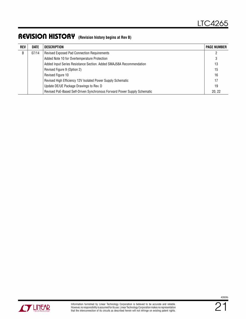
revision hisToryREV DATE DESCRIPTION PAGE NUMBER
B 07/14 Revised Exposed Pad Connection RequirementsAdded Note 10 for Overtemperature ProtectionAdded Input Series Resistance Section. Added SMAJ58A RecommendationRevised Figure 9 (Option 2)Revised Figure 10Revised High Efficiency 12V Isolated Power Supply SchematicUpdate DE/UE Package Drawings to Rev. DRevised PoE-Based Self-Driven Synchronous Forward Power Supply Schematic
23
1315161719
20, 22
(Revision history begins at Rev B)

LTC4265
224265fb
For more information www.linear.com/LTC4265
Linear Technology Corporation1630 McCarthy Blvd., Milpitas, CA 95035-7417 (408) 432-1900 FAX: (408) 434-0507 www.linear.com LINEAR TECHNOLOGY CORPORATION 2008
LT 0714 REV B • PRINTED IN USA
relaTeD parTsPART NUMBER DESCRIPTION COMMENTS
LTC4257-1 IEEE 802.3af PD Interface Controller Internal 100V, 400mA Switch, Dual Current Limit, Programmable Class
LTC4263 Single IEEE 802.3af PSE Controller Internal FET Switch
LTC4266 Quad IEEE PoE/PoE+/LTPoE++ PSE Controller With Programmable ICUT/ILIM, 2-Event Classification, Provides Up to 90W
LTC4267-3 IEEE 802.3af PD Interface with Integrated Switching Regulator
Internal 100V, 400mA Switch, Programmable Class, 300kHz Constant Frequency PWM
LTC4269 IEEE 802.3af PD Interface with Integrated Switching Regulator
2-Event Classification, Programmable Class, Synchronous Flyback/Forward Controller, Aux Support
LTC4270/LTC4271 12-Port PoE/PoE+/LTPoE++ PSE Controller Transformer Isolation, Supports IEEE 802.3af, IEEE 802.3at and LTPoE++ PDs
LTC4274 Single IEEE PoE/PoE+/LTPoE++ PSE Controller With Programmable ICUT/ILIM, 2-Event Classification, Provides Up to 90W
LT4275 PoE/PoE+/LTPoE++ PD Interface Controller External MOSFET, Up to 90W, –40°C to 125°C Operation
LTC4278 IEEE 802.3af PD Interface with Integrated Flyback Switching Regulator
2-Event Classification, Programmable Class, Synchronous No-Opto Flyback Controller, 50kHz to 250kHz, 12V Aux Support
LTC4290/LTC4271 8-Port PoE/PoE+/LTPoE++ PSE Controller Transformer Isolation, Supports IEEE 802.3af, IEEE 802.3at and LTPoE++ PDs
•
•
FDS2582
10.0k
33k
10µF16V
237k
30.9Ω
B1100
82k 158k332k
22.1k 1.2k
4.7nF
100pF
10µF100V
0.1µF100V
SMAJ58A
B1100 × 8 PLCS2.2µF100V
PA2431NL
4265 TA03a
PGND GND
SD_VSEC
OC
ISENSE
COMP
FB
VREF
SS_MAXDC
OUT
BLANK DELAY ROSC
LT1952
VIN
VCC
SOUT
GND
RCLASS
SHDN
LTC4265
T2PSE
VIN VOUT
10µH
–54VFROMDATAPAIR
–54VFROM
SPAREPAIR
•5V5A
220µF6.3VPSLVOJ227M(12)
FDS8880FDS8880
+
GND
GND 5V
2.2nF2kV
BAS516
BAS516 10k
133Ω
0.1µF
1mHDO1608C-105
IRF6217
4.7nF250V
50mΩ
5.1Ω
158k 0.22µF
5.1Ω
1nF
5.1Ω
1nF
6.8µHPG0702.682
+
2k
PS2801-1-L
PS22801-1-L
BC857BF
TLV431A
1.5k
33k 22k
0.1µF
10nF
11.3k
3.65k
51k 20k
T2P (TO MICRO
CONTROLLER)
BAS516
BAS51618VPDZ18B
VCC
PoE-Based Self-Driven Synchronous Forward Power SupplyTypical applicaTion
LOAD (A)0.5
EFFI
CIEN
CY (%
)
80
85
90
5
4265 TA03b
75
65
70
1.5 21 32.5 4 4.53.5
95
42V50V57V
Efficiency vs Load Current