ltm4643 ultrathin quad µmodule regulator with configurable ... filethe ltm®4643 is a quad dc/dc...
TRANSCRIPT
LTM4643
14643fb
For more information www.linear.com/LTM4643
n Quad Output Step-Down µModule® Regulator with 3A per Output
n Wide Input Voltage Range: 4V to 20V n 2.375V to 20V with External Bias
n 0.6V to 3.3V Output Voltagen 3A DC Output Current Each Channeln ±1.5% Total Output Voltage Regulationn Current Mode Control, Fast Transient Responsen Parallelable for Higher Output Currentn Output Voltage Trackingn Internal Temperature Sensing Diode Outputn External Frequency Synchronizationn Overvoltage, Current and Temperature Protectionn 9mm × 15mm × 1.82mm LGA and 9mm × 15mm ×
2.42mm BGA Packages
TYPICAL APPLICATION
FEATURES DESCRIPTION
Ultrathin Quad µModule Regulator with Configurable
3A Output Array
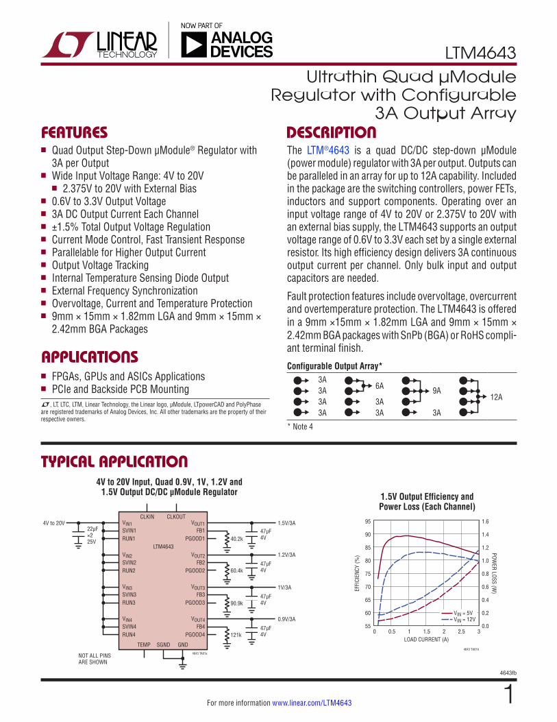
The LTM®4643 is a quad DC/DC step-down µModule (power module) regulator with 3A per output. Outputs can be paralleled in an array for up to 12A capability. Included in the package are the switching controllers, power FETs, inductors and support components. Operating over an input voltage range of 4V to 20V or 2.375V to 20V with an external bias supply, the LTM4643 supports an output voltage range of 0.6V to 3.3V each set by a single external resistor. Its high efficiency design delivers 3A continuous output current per channel. Only bulk input and output capacitors are needed.
Fault protection features include overvoltage, overcurrent and overtemperature protection. The LTM4643 is offered in a 9mm ×15mm × 1.82mm LGA and 9mm × 15mm × 2.42mm BGA packages with SnPb (BGA) or RoHS compli-ant terminal finish.
Configurable Output Array*3A3A3A3A
6A
3A3A
9A
3A
12A
* Note 4
1.5V Output Efficiency andPower Loss (Each Channel)
APPLICATIONSn FPGAs, GPUs and ASICs Applications n PCIe and Backside PCB Mounting
4V to 20V Input, Quad 0.9V, 1V, 1.2V and 1.5V Output DC/DC µModule Regulator
L, LT, LTC, LTM, Linear Technology, the Linear logo, µModule, LTpowerCAD and PolyPhase are registered trademarks of Analog Devices, Inc. All other trademarks are the property of their respective owners.
4643 TA01a
VIN1SVIN1RUN1
VIN2SVIN2RUN2
VIN3SVIN3RUN3
VIN4SVIN4RUN4
SGND
LTM4643
CLKIN
22µF×225V
CLKOUT
TEMP GND
VOUT1FB1
PGOOD1
VOUT2FB2
PGOOD2
VOUT3FB3
PGOOD3
VOUT4FB4
PGOOD4
47µF4V
1.5V/3A4V to 20V
40.2k
47µF4V
1.2V/3A
60.4k
47µF4V
1V/3A
90.9k
47µF4V
0.9V/3A
121k
NOT ALL PINSARE SHOWN
LOAD CURRENT (A)0
55
EFFI
CIEN
CY (%
)
POWER LOSS (W
)
75
80
85
95
1
4643 TA01b
70
65
60
90
0.0
0.6
0.4
0.2
1.2
1.0
0.8
1.6
1.4
320.5 1.5 2.5
VIN = 5VVIN = 12V
LTM4643
24643fb
For more information www.linear.com/LTM4643
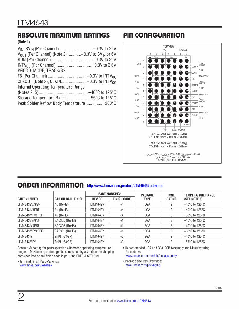
ABSOLUTE MAXIMUM RATINGS
VIN, SVIN (Per Channel) .............................. –0.3V to 22VVOUT (Per Channel) (Note 3) ............–0.3V to SVIN or 6VRUN (Per Channel) ..................................... –0.3V to 22VINTVCC (Per Channel) ............................... –0.3V to 3.6VPGOOD, MODE, TRACK/SS, FB (Per Channel) ...................................–0.3V to INTVCCCLKOUT (Note 3), CLKIN .......................–0.3V to INTVCCInternal Operating Temperature Range(Notes 2, 5) ............................................ –40°C to 125°CStorage Temperature Range .................. –55°C to 125°CPeak Solder Reflow Body Temperature ................. 260°C
(Note 1)
ORDER INFORMATION
LGA PACKAGE (WEIGHT = 0.70g)77-LEAD (9mm × 15mm × 1.82mm)
BGA PACKAGE (WEIGHT = 0.83g)77-LEAD (9mm × 15mm × 2.42mm)
1 2 3 4 5 6 7
B
C
D
E
F
G
H
J
K
L
A
TOP VIEW
VOUT1
SVIN1MODE1
RUN1
COMP1
INTVCC1
GND
PGOOD2 PGOOD1
INTVCC2PGOOD3 TEMP
INTVCC3
PGOOD4 CLKOUT
FB1
TRACK/SS1
GND
CLKIN
TRACK/SS2FB2
RUN2SGND
TRACK/SS3FB3
TRACK/SS4
INTVCC4
RUN4
MODE2SVIN2
COMP2
RUN3FB4
MODE3SVIN3
COMP3
COMP4
MODE4SVIN4VIN4
VIN1
GND
GND
GND
VIN3
VIN2
VOUT4
VOUT3
VOUT2
TJMAX = 125°C, θJCtop = 17°C/W, θJCbottom = 2.75°C/W,
θJB + θBA = 11°C/W, θJA = 10°C/W θ VALUES PER JESD 51-12
PIN CONFIGURATION
PART NUMBER PAD OR BALL FINISHPART MARKING* PACKAGE
TYPEMSL
RATINGTEMPERATURE RANGE (SEE NOTE 2)DEVICE FINISH CODE
LTM4643EV#PBF Au (RoHS) LTM4643V e4 LGA 3 –40°C to 125°CLTM4643IV#PBF Au (RoHS) LTM4643V e4 LGA 3 –40°C to 125°CLTM4643MPV#PBF Au (RoHS) LTM4643V e4 LGA 3 –55°C to 125°CLTM4643EY#PBF SAC305 (RoHS) LTM4643Y e1 BGA 3 –40°C to 125°CLTM4643IY#PBF SAC305 (RoHS) LTM4643Y e1 BGA 3 –40°C to 125°CLTM4643MPY#PBF SAC305 (RoHS) LTM4643Y e1 BGA 3 –55°C to 125°CLTM4643IY SnPb (63/37) LTM4643Y e0 BGA 3 –40°C to 125°CLTM4643MPY SnPb (63/37) LTM4643Y e0 BGA 3 –55°C to 125°C
Consult Marketing for parts specified with wider operating temperature ranges. *Device temperature grade is indicated by a label on the shipping container. Pad or ball finish code is per IPC/JEDEC J-STD-609.• Terminal Finish Part Markings:
www.linear.com/leadfree
• Recommended LGA and BGA PCB Assembly and Manufacturing Procedures: www.linear.com/umodule/pcbassembly
• Package and Tray Drawings: www.linear.com/packaging
http://www.linear.com/product/LTM4643#orderinfo
LTM4643
34643fb
For more information www.linear.com/LTM4643
ELECTRICAL CHARACTERISTICS The l denotes the specifications which apply over the specified internal operating junction temperature range, otherwise specifications are at TA = 25°C (Note 2). VIN = 12V, per the typical application.
SYMBOL PARAMETER CONDITIONS MIN TYP MAX UNITS
Switching Regulator Section: per Channel
VIN, SVIN Input DC Voltage SVIN = VIN l 4 20 V
VOUT(RANGE) Output Voltage Range l 0.6 3.3 V
VOUT(DC) Output Voltage, Total Variation with Line and Load
CIN = 22µF, COUT = 100µF Ceramic, RFB = 40.2k, MODE = INTVCC,VIN = 4V to 20V, IOUT = 0A to 3A (Note 4)
l
1.477
1.50
1.523
V
VRUN RUN Pin On Threshold VRUN Rising 1.1 1.2 1.3 V
IQ(SVIN) Input Supply Bias Current VIN = 12V, VOUT = 1.5V, MODE = INTVCC VIN = 12V, VOUT = 1.5V, MODE = GND Shutdown, RUN = 0, VIN = 12V
6 2
11
mA mA µA
IS(VIN) Input Supply Current VIN = 12V, VOUT = 1.5V, IOUT = 3A 0.45 A
IOUT(DC) Output Continuous Current Range VIN = 12V, VOUT = 1.5V (Note 4) 0 3 A
ΔVOUT (Line)/VOUT Line Regulation Accuracy VOUT = 1.5V, VIN = 4V to 20V, IOUT = 0A l 0.01 0.05 %/V
ΔVOUT (Load)/VOUT Load Regulation Accuracy VOUT = 1.5V, IOUT = 0A to 3A l 0.5 1.0 %
VOUT(AC) Output Ripple Voltage IOUT = 0A, COUT = 100µF Ceramic, VIN = 12V, VOUT = 1.5V
5 mV
ΔVOUT(START) Turn-On Overshoot IOUT = 0A, COUT = 100µF Ceramic, VIN = 12V, VOUT = 1.5V
30 mV
tSTART Turn-On Time COUT = 100µF Ceramic, No Load, TRACK/SS = 0.01µF, VIN = 12V, VOUT = 1.5V
2.5 ms
ΔVOUTLS Peak Deviation for Dynamic Load Load: 0% to 50% to 0% of Full Load, COUT = 47µF Ceramic, VIN = 12V, VOUT = 1.5V
160 mV
tSETTLE Settling Time for Dynamic Load Step
Load: 0% to 50% to 0% of Full Load, COUT = 47µF Ceramic, VIN = 12V, VOUT = 1.5V
40 µs
IOUTPK Output Current Limit VIN = 12V, VOUT = 1.5V 3.5 5 A
VFB Voltage at FB Pin IOUT = 0A, VOUT = 1.5V, –40°C to 125°C l 0.593 0.60 0.607 V
IFB Current at FB Pin (Note 3) ±30 nA
RFBHI Resistor Between VOUT and FB Pins
60.05 60.40 60.75 kΩ
ITRACK/SS Track Pin Soft-Start Pull-Up Current
TRACK/SS = 0V 2.5 4 µA
VIN(UVLO) VIN Undervoltage Lockout VIN Falling VIN Hysteresis
2.4 2.6 350
2.8 V mV
tON(MIN) Minimum On-Time (Note 3) 40 ns
tOFF(MIN) Minimum Off-Time (Note 3) 70 ns
VPGOOD PGOOD Trip Level VFB With Respect to Set Output VFB Ramping Negative VFB Ramping Positive
–13 7
–10 10
–7 13
% %
IPGOOD PGOOD Leakage 2 µA
VPGL PGOOD Voltage Low IPGOOD = 1mA 0.02 0.1 V
VINTVCC Internal VCC Voltage SVIN = 4V to 20V 3.1 3.3 3.4 V
VINTVCC Load Reg INTVCC Load Regulation ICC = 0mA to 20mA 0.5 %
fOSC Oscillator Frequency 1.2 MHz
CLKIN CLKIN Threshold 0.7 V
LTM4643
44643fb
For more information www.linear.com/LTM4643
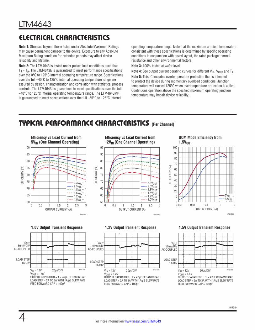
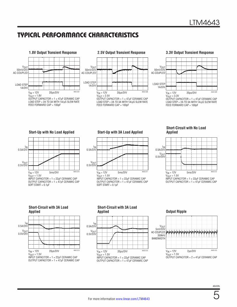
1.0V Output Transient Response 1.2V Output Transient Response 1.5V Output Transient Response
Efficiency vs Load Current from 5VIN (One Channel Operating)
Efficiency vs Load Current from 12VIN (One Channel Operating)
DCM Mode Efficiency from 1.5VOUT
ELECTRICAL CHARACTERISTICSNote 1: Stresses beyond those listed under Absolute Maximum Ratings may cause permanent damage to the device. Exposure to any Absolute Maximum Rating condition for extended periods may affect device reliability and lifetime.Note 2: The LTM4643 is tested under pulsed load conditions such that TJ ≈ TA. The LTM4643E is guaranteed to meet performance specifications over the 0°C to 125°C internal operating temperature range. Specifications over the full –40°C to 125°C internal operating temperature range are assured by design, characterization and correlation with statistical process controls. The LTM4643I is guaranteed to meet specifications over the full –40°C to 125°C internal operating temperature range. The LTM4643MP is guaranteed to meet specifications over the full –55°C to 125°C internal
operating temperature range. Note that the maximum ambient temperature consistent with these specifications is determined by specific operating conditions in conjunction with board layout, the rated package thermal resistance and other environmental factors.Note 3: 100% tested at wafer level.Note 4: See output current derating curves for different VIN, VOUT and TA.Note 5: This IC includes overtemperature protection that is intended to protect the device during momentary overload conditions. Junction temperature will exceed 125°C when overtemperature protection is active. Continuous operation above the specified maximum operating junction temperature may impair device reliability.
TYPICAL PERFORMANCE CHARACTERISTICS
OUTPUT CURRENT (A)0
60
65
EFFI
CIEN
CY (%
)
70
80
85
90
100
95
10.5 1.5
4643 G01
75
32 2.5
3.3VOUT2.5VOUT1.8VOUT1.5VOUT1.2VOUT1.0VOUT
OUTPUT CURRENT (A)0
55
60
65
EFFI
CIEN
CY (%
)
70
80
85
90
95
10.5 1.5
4643 G02
75
32 2.5
3.3VOUT2.5VOUT1.8VOUT1.5VOUT1.2VOUT1.0VOUT
LOAD CURRENT (A)0.0010
EFFI
CIEN
CY (%
)
20
30
40
100
0.01
4643 G03
10
50
60
70
80
90
100.1 1
5VIN12VIN
VOUT50mV/DIV
AC-COUPLED
LOAD STEP1A/DIV
VIN = 12VVOUT = 1.0VOUTPUT CAPACITOR = 1 × 47µF CERAMIC CAPLOAD STEP = 2A TO 3A WITH 1A/µS SLEW RATEFEED FORWARD CAP = 100pF
20µs/DIV 4643 G04
(Per Channel)
VOUT50mV/DIV
AC-COUPLED
LOAD STEP1A/DIV
VIN = 12VVOUT = 1.2VOUTPUT CAPACITOR = 1 × 47µF CERAMIC CAPLOAD STEP = 2A TO 3A WITH 1A/µS SLEW RATEFEED FORWARD CAP = 100pF
20µs/DIV 4643 G05
VOUT50mV/DIV
AC-COUPLED
LOAD STEP1A/DIV
VIN = 12VVOUT = 1.5VOUTPUT CAPACITOR = 1 × 47µF CERAMIC CAPLOAD STEP = 2A TO 3A WITH 1A/µS SLEW RATEFEED FORWARD CAP = 100pF
20µs/DIV 4643 G06
LTM4643
54643fb
For more information www.linear.com/LTM4643
TYPICAL PERFORMANCE CHARACTERISTICS
1.8V Output Transient Response 2.5V Output Transient Response 3.3V Output Transient Response
Start-Up with No Load Applied Start-Up with 3A Load AppliedShort-Circuit with No Load Applied
VOUT50mV/DIV
AC-COUPLED
LOAD STEP1A/DIV
VIN = 12VVOUT = 2.5VOUTPUT CAPACITOR = 1 × 47µF CERAMIC CAPLOAD STEP = 2A TO 3A WITH 1A/µS SLEW RATEFEED FORWARD CAP = 100pF
20µs/DIV 4643 G08
VOUT50mV/DIV
AC-COUPLED
LOAD STEP1A/DIV
VIN = 12VVOUT = 3.3VOUTPUT CAPACITOR = 1 × 47µF CERAMIC CAPLOAD STEP = 2A TO 3A WITH 1A/µS SLEW RATEFEED FORWARD CAP = 100pF
20µs/DIV 4643 G09
IIN0.5A/DIV
VOUT0.5V/DIV
VIN = 12VVOUT = 1.5VINPUT CAPACITOR = 1 × 22µF CERAMIC CAPOUTPUT CAPACITOR = 1 × 47µF CERAMIC CAPSOFT START = 0.1µF
5ms/DIV 4643 G10
IIN0.5A/DIV
VOUT0.5V/DIV
VIN = 12VVOUT = 1.5VINPUT CAPACITOR = 1 × 22µF CERAMIC CAPOUTPUT CAPACITOR = 1 × 47µF CERAMIC CAPSOFT START = 0.1µF
5ms/DIV 4643 G11
IIN0.5A/DIV
VOUT0.5V/DIV
VIN = 12VVOUT = 1.5VINPUT CAPACITOR = 1 × 22µF CERAMIC CAPOUTPUT CAPACITOR = 1 × 47µF CERAMIC CAP
5ms/DIV 4643 G12
VIN = 12VVOUT = 1.8VOUTPUT CAPACITOR = 1 × 47µF CERAMIC CAPLOAD STEP = 2A TO 3A WITH 1A/µS SLEW RATEFEED FORWARD CAP = 100pF
20µs/DIV 4643 G07
VOUT50mV/DIV
AC-COUPLED
LOAD STEP1A/DIV
Short-Circuit with 3A Load Applied
Short-Circuit with 3A Load Applied
IIN0.5A/DIV
VOUT0.5V/DIV
VIN = 12VVOUT = 1.5VINPUT CAPACITOR = 1 × 22µF CERAMIC CAPOUTPUT CAPACITOR = 1 × 47µF CERAMIC CAP
20µs/DIV 4643 G13
IIN0.5A/DIV
VOUT0.5V/DIV
VIN = 12VVOUT = 1.5VINPUT CAPACITOR = 1 × 22µF CERAMIC CAPOUTPUT CAPACITOR = 1 × 47µF CERAMIC CAP
20µs/DIV 4643 G14
Output Ripple
VOUT5mV/DIV
AC-COUPLED350kHz
BANDWIDTH
VIN = 12VVOUT = 1.5VOUTPUT CAPACITOR = 2 × 47µF CERAMIC CAP
2µs/DIV 4643 G15
LTM4643
64643fb
For more information www.linear.com/LTM4643
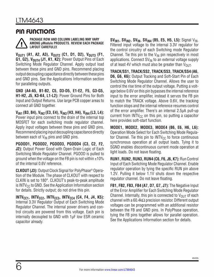
PIN FUNCTIONS
VOUT1 (A1, A2, A3), VOUT2 (C1, D1, D2), VOUT3 (F1, G1, G2), VOUT4 (J1, K1, K2): Power Output Pins of Each Switching Mode Regulator Channel. Apply output load between these pins and GND pins. Recommend placing output decoupling capacitance directly between these pins and GND pins. See the Applications Information section for paralleling outputs.
GND (A4-A5, B1-B2, C5, D3-D5, E1-E2, F5, G3-G5, H1-H2, J5, K3-K4, L1-L2): Power Ground Pins for Both Input and Output Returns. Use large PCB copper areas to connect all GND together.
VIN1 (B3, B4), VIN2 (E3, E4), VIN3 (H3, H4), VIN4 (L3, L4): Power input pins connect to the drain of the internal top MOSFET for each switching mode regulator channel. Apply input voltages between these pins and GND pins. Recommend placing input decoupling capacitance directly between each of VIN pins and GND pins.
PGOOD1, PGOOD2, PGOOD3, PGOOD4 (C3, C2, F2, J2): Output Power Good with Open-Drain Logic of Each Switching Mode Regulator Channel. PGOOD is pulled to ground when the voltage on the FB pin is not within ±10% of the internal 0.6V reference.
CLKOUT (J3): Output Clock Signal for PolyPhase® Opera-tion of the Module. The phase of CLKOUT with respect to CLKIN is set to 180°. CLKOUT’s peak-to-peak amplitude is INTVCC to GND. See the Application Information section for details. Strictly output; do not drive this pin.
INTVCC1, INTVCC2, INTVCC3, INTVCC4 (C4, F4, J4, K5): Internal 3.3V Regulator Output of Each Switching Mode Regulator Channel. The internal power drivers and con-trol circuits are powered from this voltage. Each pin is internally decoupled to GND with 1µF low ESR ceramic capacitor already.
SVIN1, SVIN2, SVIN, SVIN4 (B5, E5, H5, L5): Signal VIN. Filtered input voltage to the internal 3.3V regulator for the control circuitry of each Switching mode Regulator Channel. Tie this pin to the VIN pin respectively in most applications. Connect SVIN to an external voltage supply of at least 4V which must also be greater than VOUT.
TRACK/SS1, TRACK/SS2, TRACK/SS3, TRACK/SS4 (A6, D6, G6, K6): Output Tracking and Soft-Start Pin of Each Switching Mode Regulator Channel. Allows the user to control the rise time of the output voltage. Putting a volt-age below 0.6V on this pin bypasses the internal reference input to the error amplifier, instead it servos the FB pin to match the TRACK voltage. Above 0.6V, the tracking function stops and the internal reference resumes control of the error amplifier. There’s an internal 2.5µA pull-up current from INTVCC on this pin, so putting a capacitor here provides soft-start function.
MODE1, MODE2, MODE3, MODE4 (B6, E6, H6, L6): Operation Mode Select for Each Switching Mode Regula-tor Channel. Tie this pin to INTVCC to force continuous synchronous operation at all output loads. Tying it to SGND enables discontinuous current mode operation at light loads. Do not leave floating.
RUN1, RUN2, RUN3, RUN4 (C6, F6, J6, K7): Run Control Input of Each Switching Mode Regulator Channel. Enable regulator operation by tying the specific RUN pin above 1.2V. Pulling it below 1.1V shuts down the respective regulator channel. Do not leave floating.
FB1, FB2, FB3, FB4 (A7, D7, G7, J7): The Negative Input of the Error Amplifier for Each Switching Mode Regulator Channel. Internally, this pin is connected to VOUT of each channel with a 60.4kΩ precision resistor. Different output voltages can be programmed with an additional resistor between the FB and GND pins. In PolyPhase operation, tying the FB pins together allows for parallel operation. See the Applications Information section for details.
PACKAGE ROW AND COLUMN LABELING MAY VARY AMONG µModule PRODUCTS. REVIEW EACH PACKAGE LAYOUT CAREFULLY.
LTM4643
74643fb
For more information www.linear.com/LTM4643
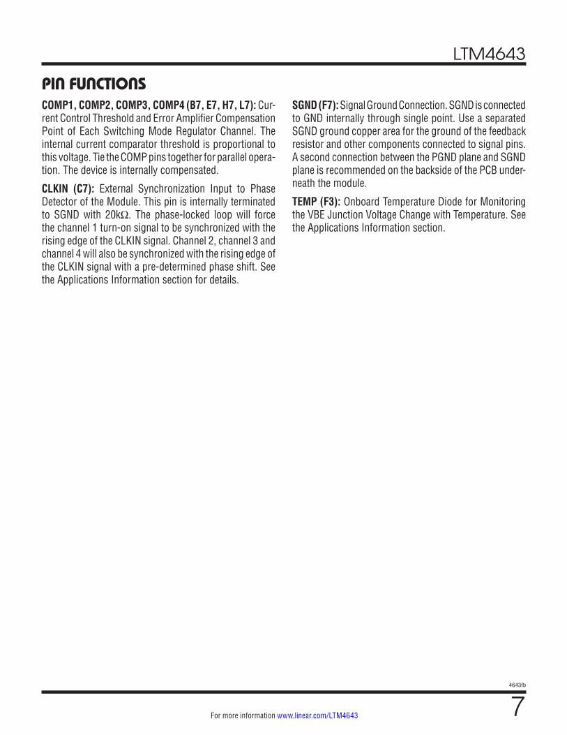
PIN FUNCTIONSCOMP1, COMP2, COMP3, COMP4 (B7, E7, H7, L7): Cur-rent Control Threshold and Error Amplifier Compensation Point of Each Switching Mode Regulator Channel. The internal current comparator threshold is proportional to this voltage. Tie the COMP pins together for parallel opera-tion. The device is internally compensated.
CLKIN (C7): External Synchronization Input to Phase Detector of the Module. This pin is internally terminated to SGND with 20kΩ. The phase-locked loop will force the channel 1 turn-on signal to be synchronized with the rising edge of the CLKIN signal. Channel 2, channel 3 and channel 4 will also be synchronized with the rising edge of the CLKIN signal with a pre-determined phase shift. See the Applications Information section for details.
SGND (F7): Signal Ground Connection. SGND is connected to GND internally through single point. Use a separated SGND ground copper area for the ground of the feedback resistor and other components connected to signal pins. A second connection between the PGND plane and SGND plane is recommended on the backside of the PCB under-neath the module.
TEMP (F3): Onboard Temperature Diode for Monitoring the VBE Junction Voltage Change with Temperature. See the Applications Information section.
LTM4643
84643fb
For more information www.linear.com/LTM4643
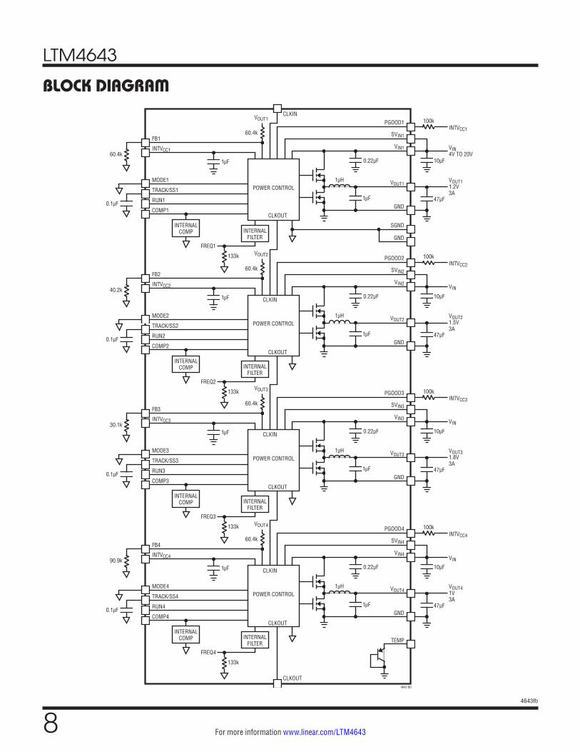
BLOCK DIAGRAM
4643 BD
POWER CONTROL
CLKOUT
FB1
CLKIN
MODE1
TRACK/SS1
RUN1
COMP1
INTVCC1
INTERNALFILTER
INTERNALCOMP
VOUT1
1µF
0.22µF
1µH
100k
100k
100k
100k
10µF
47µF
FREQ1
133k
60.4k
60.4k
0.1µF
VIN4V TO 20V
VOUT11.2V3A
INTVCC1PGOOD1
SVIN1
VIN1
VOUT1
GND
SGND
GND
POWER CONTROL
FB2
MODE2
TRACK/SS2
RUN2
COMP2
INTVCC2
INTERNALFILTER
INTERNALCOMP
VOUT2
1µF
0.22µF
1µH
10µF
47µF
FREQ2
133k
60.4k
40.2k
0.1µF
VIN
VOUT21.5V3A
INTVCC2PGOOD2
SVIN2
VIN2
VOUT2
GND
POWER CONTROL
FB3
MODE3
TRACK/SS3
RUN3
COMP3
INTVCC3
INTERNALFILTER
INTERNALCOMP
VOUT3
1µF
0.22µF
1µH
10µF
47µF
FREQ3
133k
60.4k
30.1k
0.1µF
VIN
VOUT31.8V3A
INTVCC3PGOOD3
SVIN3
VIN3
VOUT3
GND
POWER CONTROL
FB4
MODE4
TRACK/SS4
RUN4
COMP4
INTVCC4
INTERNALFILTER
INTERNALCOMP
VOUT4
1µF
0.22µF
1µH
10µF
47µF
1µF
FREQ4
133k
60.4k
90.9k
0.1µF
VIN
VOUT41V3A
INTVCC4PGOOD4
SVIN4
VIN4
VOUT4
GND
TEMP
CLKOUT
CLKOUT
CLKIN
CLKOUT
CLKIN
CLKOUT
CLKIN
1µF
1µF
1µF
LTM4643
94643fb
For more information www.linear.com/LTM4643
SYMBOL PARAMETER CONDITIONS MIN TYP MAX UNITS
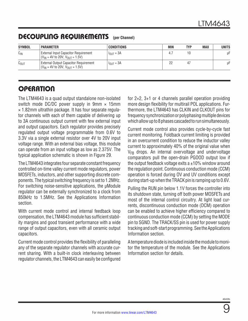
CIN External Input Capacitor Requirement (VIN = 4V to 20V, VOUT = 1.5V)
IOUT = 3A 4.7 10 µF
COUT External Output Capacitor Requirement (VIN = 4V to 20V, VOUT = 1.5V)
IOUT = 3A 22 47 µF
DECOUPLING REQUIREMENTS
OPERATIONThe LTM4643 is a quad output standalone non-isolated switch mode DC/DC power supply in 9mm × 15mm × 1.82mm ultrathin package. It has four separate regula-tor channels with each of them capable of delivering up to 3A continuous output current with few external input and output capacitors. Each regulator provides precisely regulated output voltage programmable from 0.6V to 3.3V via a single external resistor over 4V to 20V input voltage range. With an external bias voltage, this module can operate from an input voltage as low as 2.375V. The typical application schematic is shown in Figure 29.
The LTM4643 integrates four separate constant frequency controlled on-time valley current mode regulators, power MOSFETs, inductors, and other supporting discrete com-ponents. The typical switching frequency is set to 1.2MHz. For switching noise-sensitive applications, the µModule regulator can be externally synchronized to a clock from 850kHz to 1.5MHz. See the Applications Information section.
With current mode control and internal feedback loop compensation, the LTM4643 module has sufficient stabil-ity margins and good transient performance with a wide range of output capacitors, even with all ceramic output capacitors.
Current mode control provides the flexibility of paralleling any of the separate regulator channels with accurate cur-rent sharing. With a built-in clock interleaving between regulator channels, the LTM4643 can easily be configured
for 2+2, 3+1 or 4 channels parallel operation providing more design flexibility for multirail POL applications. Fur-thermore, the LTM4643 has CLKIN and CLKOUT pins for frequency synchronization or polyphasing multiple devices which allow up to 8 phases cascaded to run simultaneously.
Current mode control also provides cycle-by-cycle fast current monitoring. Foldback current limiting is provided in an overcurrent condition to reduce the inductor valley current to approximately 40% of the original value when VFB drops. An internal overvoltage and undervoltage comparators pull the open-drain PGOOD output low if the output feedback voltage exits a ±10% window around the regulation point. Continuous conduction mode (CCM) operation is forced during OV and UV conditions except during start-up when the TRACK pin is ramping up to 0.6V.
Pulling the RUN pin below 1.1V forces the controller into its shutdown state, turning off both power MOSFETs and most of the internal control circuitry. At light load cur-rents, discontinuous conduction mode (DCM) operation can be enabled to achieve higher efficiency compared to continuous conduction mode (CCM) by setting the MODE pin to SGND. The TRACK/SS pin is used for power supply tracking and soft-start programming. See the Applications Information section.
A temperature diode is included inside the module to moni-tor the temperature of the module. See the Applications Information section for details.
(per Channel)
LTM4643
104643fb
For more information www.linear.com/LTM4643
APPLICATIONS INFORMATIONThe typical LTM4643 application circuit is shown in Figure 29. External component selection is primarily determined by the input voltage, the output voltage and the maximum load current. Refer to Table 6 for specific external capacitor requirements for a particular application.
VIN to VOUT Step-Down Ratios
There are restrictions in the maximum VIN and VOUT step-down ratio that can be achieved for a given input voltage due to the minimum off-time and minimum on-time limits of each regulator. The minimum off-time limit imposes a maximum duty cycle which can be calculated as:
DMAX = 1 – tOFF(MIN) • fSW
where tOFF(MIN) is the minimum off-time, 70ns typical for LTM4643, and fSW is the switching frequency. Conversely the minimum on-time limit imposes a minimum duty cycle of the converter which can be calculated as:
DMIN = tON(MIN) • fSW
where tON(MIN) is the minimum on-time, 40ns typical for LTM4643. In the rare cases where the minimum duty cycle is surpassed, the output voltage will still remain in regulation, but the switching frequency will decrease from its programmed value. Note that additional thermal derating may be applied. See the Thermal Considerations and Output Current Derating section in this data sheet.
Output Voltage Programming
The PWM controller has an internal 0.6V reference voltage. As shown in the Block Diagram, a 60.4k internal feedback resistor connects each regulator channel from VOUT pin to FB pin. Adding a resistor RFB from FB pin to GND programs the output voltage:
RFB =60.4k
VOUT
0.6− 1
Table 1. VFB Resistor Table vs Various Output VoltagesVOUT (V) 0.6 1.0 1.2 1.5 1.8 2.5 3.3
RFB (k) Open 90.9 60.4 40.2 30.1 19.1 13.3
For parallel operation of N channels, use the following equation can be used to solve for RFB. Tie the VOUT and
the FB and COMP pins together for each paralleled output with a single resistor to GND as determined by:
RFB =
60.4kN
VOUT
0.6– 1
Input Decoupling Capacitors
The LTM4643 module should be connected to a low AC-impedance DC source. For each regulator channel, a 10µF input ceramic capacitor is recommended for RMS ripple current decoupling. A bulk input capacitor is only needed when the input source impedance is compromised by long inductive leads, traces or not enough source capacitance. The bulk capacitor can be an electrolytic aluminum capaci-tor or polymer capacitor.
Without considering the inductor ripple current, the RMS current of the input capacitor can be estimated as:
ICIN(RMS) =
IOUT(MAX)
η%• D •(1− D)
where η% is the estimated efficiency of the power module.
Output Decoupling Capacitors
With an optimized high frequency, high bandwidth design, only single piece of low ESR output ceramic capacitor is required for each regulator channel to achieve low output voltage ripple and very good transient response. Additional output filtering may be required by the system designer, if further reduction of output ripples or dynamic transient spikes is required. Table 6 provides a reference matrix show-ing transient performance for different output capacitor con-figurations. Multiphase operation will reduce effective out-put ripple as a function of the number of phases. Application Note 77 discusses this noise reduction versus output ripple current cancellation, but the output capacitance will be more a function of stability and transient response. The LTpowerCAD® Design Tool is available to download online for output ripple, stability and transient response analysis and calculating the output ripple reduction as the number of phases implemented increases by N times.
LTM4643
114643fb
For more information www.linear.com/LTM4643
APPLICATIONS INFORMATIONDiscontinuous Conduction Mode (DCM)
In applications where low output ripple and high efficiency at intermediate current are desired, discontinuous con-duction mode (DCM) should be used by connecting the MODE pin to SGND. At light loads the internal current comparator may remain tripped for several cycles and force the top MOSFET to stay off for several cycles, thus skipping cycles. The inductor current does not reverse in this mode.
Force Continuous Conduction Mode (CCM)
In applications where fixed frequency operation is more critical than low current efficiency, and where the lowest output ripple is desired, forced continuous conduction mode operation should be used. Forced continuous opera-tion can be enabled by tying the MODE pin to INTVCC. In this mode, inductor current is allowed to reverse during low output loads, the COMP voltage is in control of the current comparator threshold throughout, and the top MOSFET always turns on with each oscillator pulse. During start-up, forced continuous mode is disabled and inductor current is prevented from reversing until the LTM4643’s output voltage is in regulation.
Operating Frequency
The operating frequency of the LTM4643 is optimized to achieve the compact package size and the minimum output ripple voltage while still keeping high efficiency. The default operating frequency is internally set to 1.2MHz. In most applications, no additional frequency adjusting is required.
If any operating frequency other than 1.2MHz is required by application, the µModule regulator can be externally synchronized to a clock from 850kHz to 1.5MHz.
Please note, a minimum switching frequency is required for given VIN, VOUT operating conditions to keep a maxi-mum peak-to-peak inductor ripple current below 2A for the LTM4643. The peak-to-peak inductor ripple current can be calculated as:
ΔIPK−PK =
VOUT
FS(MHz)•
VIN – VOUT
VOUT
The maximum 2A peak-to-peak inductor ripple current is enforced due to the nature of the valley current mode control to maintain output voltage regulation at no load.
Frequency Synchronization and Clock In
The power module has a phase-locked loop comprised of an internal voltage controlled oscillator and a phase detector. This allows all internal top MOSFET turn-on to be locked to the rising edge of the same external clock. The external clock frequency range must be within ±30% around the 1.2MHz set frequency. A pulse detection circuit is used to detect a clock on the CLKIN pin to turn on the phase-locked loop. The pulse width of the clock has to be at least 100ns. The clock high level must be above 2V and clock low level below 0.3V. During the start-up of the regulator, the phase-locked loop function is disabled.
Multichannel Parallel Operation
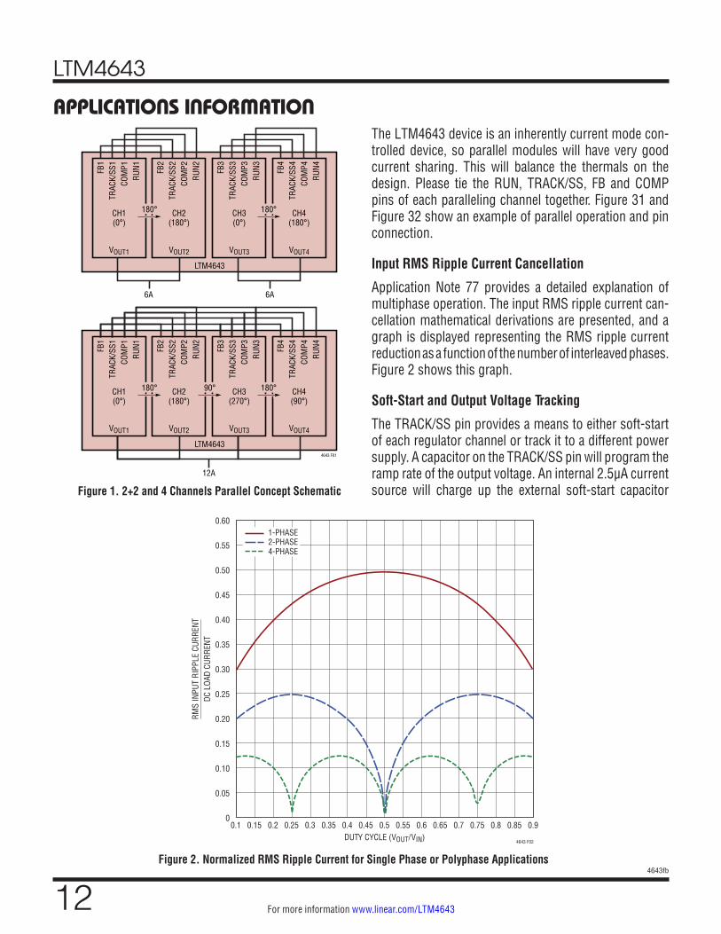
For loads that demand more than 3A of output current, the LTM4643 multiple regulator channels can be easily paralleled to provide more output current without increas-ing input and output voltage ripples. The LTM4643 has preset built-in phase shift between each two of the four regulator channels which is suitable to employ a 2+2, 3+1 or 4 channels parallel operation. Table 2 gives the phase difference between regulator channels.
Table 2. Phase Difference Between Regulator ChannelsCHANNEL CH1 CH2 CH3 CH4
Phase Difference 180° 90° 180°
Figure 1 shows a 2+2 and a 4-channels parallel concept schematic for clock phasing.
A multiphase power supply significantly reduces the amount of ripple current in both the input and output ca-pacitors. The RMS input ripple current is reduced by, and the effective ripple frequency is multiplied by, the number of phases used (assuming that the input voltage is greater than the number of phases used times the output voltage). The output ripple amplitude is also reduced by the number of phases used when all of the outputs are tied together to achieve a single high output current design.
LTM4643
124643fb
For more information www.linear.com/LTM4643
APPLICATIONS INFORMATION
Figure 2. Normalized RMS Ripple Current for Single Phase or Polyphase Applications
The LTM4643 device is an inherently current mode con-trolled device, so parallel modules will have very good current sharing. This will balance the thermals on the design. Please tie the RUN, TRACK/SS, FB and COMP pins of each paralleling channel together. Figure 31 and Figure 32 show an example of parallel operation and pin connection.
Input RMS Ripple Current Cancellation
Application Note 77 provides a detailed explanation of multiphase operation. The input RMS ripple current can-cellation mathematical derivations are presented, and a graph is displayed representing the RMS ripple current reduction as a function of the number of interleaved phases. Figure 2 shows this graph.
Soft-Start and Output Voltage Tracking
The TRACK/SS pin provides a means to either soft-start of each regulator channel or track it to a different power supply. A capacitor on the TRACK/SS pin will program the ramp rate of the output voltage. An internal 2.5µA current source will charge up the external soft-start capacitor
DUTY CYCLE (VOUT/VIN)0.1 0.15 0.2 0.25 0.3 0.35 0.4 0.45 0.5 0.55 0.6 0.65 0.7 0.75 0.8 0.85 0.9
0.60
0.55
0.50
0.45
0.40
0.35
0.30
0.25
0.20
0.15
0.10
0.05
0
4643 F02
1-PHASE2-PHASE4-PHASE
RMS
INPU
T RI
PPLE
CUR
RENT
DC L
OAD
CURR
ENT
Figure 1. 2+2 and 4 Channels Parallel Concept Schematic
4643 F01
FB1
TRAC
K/SS
1CO
MP1
RUN1
VOUT1
CH1(0°)
FB2
TRAC
K/SS
2CO
MP2
RUN2
VOUT2
LTM4643
6A 6A
CH2(180°)
180°FB
3TR
ACK/
SS3
COM
P3RU
N3VOUT3
CH3(0°)
FB4
TRAC
K/SS
4CO
MP4
RUN4
VOUT4
CH4(180°)
180°
FB1
TRAC
K/SS
1CO
MP1
RUN1
VOUT1
CH1(0°)
FB2
TRAC
K/SS
2CO
MP2
RUN2
VOUT2
LTM4643
12A
CH2(180°)
180°
FB3
TRAC
K/SS
3CO
MP3
RUN3
VOUT3
CH3(270°)
FB4
TRAC
K/SS
4CO
MP4
RUN4
VOUT4
CH4(90°)
180°90°
LTM4643
134643fb
For more information www.linear.com/LTM4643
APPLICATIONS INFORMATIONtowards the INTVCC voltage. When the TRACK/SS voltage is below 0.6V, it will take over the internal 0.6V reference voltage to control the output voltage. The total soft-start time can be calculated as:
tSS = 0.6 •
CSS
2.5µA
where CSS is the capacitance on the TRACK/SS pin. Cur-rent foldback and forced continuous mode are disabled during the soft-start process.
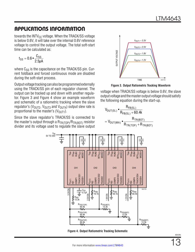
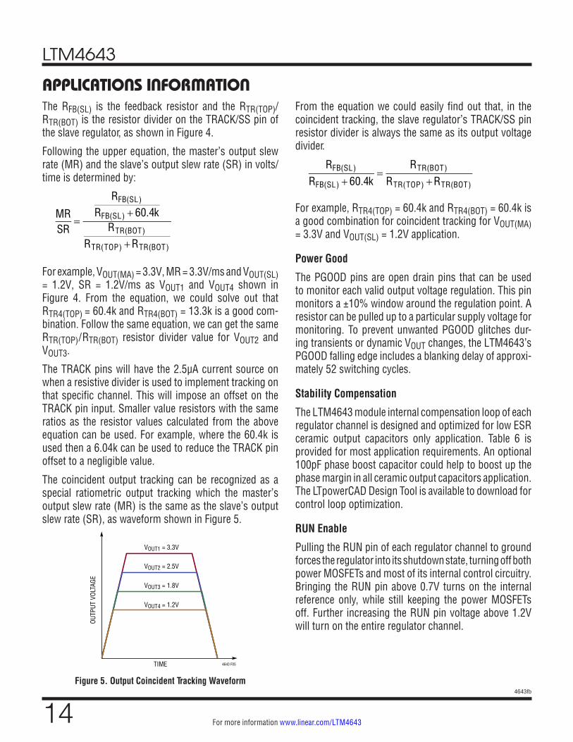
Output voltage tracking can also be programmed externally using the TRACK/SS pin of each regulator channel. The output can be tracked up and down with another regula-tor. Figure 3 and Figure 4 show an example waveform and schematic of a ratiometric tracking where the slave regulator’s (VOUT2, VOUT3 and VOUT4) output slew rate is proportional to the master’s (VOUT1).
Since the slave regulator’s TRACK/SS is connected to the master’s output through a RTR(TOP)/RTR(BOT) resistor divider and its voltage used to regulate the slave output
4643 F04
V IN1
SVIN
1RU
N1IN
TVCC
1M
ODE1
V OUT
1FB
1CO
MP1
TRAC
K/SS
1PG
OOD1
CH1
CSS0.1µF
RFB113.3k
VIN5V TO 20V
RTR2(TOP)60.4k
3.3V
/3A
2.5V
/3A
1.8V
/3A
1.2V
/3A
V IN2
SVIN
2RU
N2IN
TVCC
2M
ODE2
V OUT
2FB
2CO
MP2
TRAC
K/SS
2PG
OOD2
CH2
RFB219.1k
V IN3
SVIN
3RU
N3IN
TVCC
3M
ODE3
V OUT
3FB
3CO
MP3
TRAC
K/SS
3PG
OOD3
CH3
RFB330.1k
V IN4
SVIN
4RU
N4IN
TVCC
4M
ODE4
V OUT
4FB
4CO
MP4
TRAC
K/SS
4PG
OOD4
CH4
RFB460.4k
RTR2(BOT)13.3k
RTR3(TOP)60.4k
RTR3(BOT)13.3k
RTR4(TOP)60.4k
RTR4(BOT)13.3k
4643 F03TIME
OUTP
UT V
OLTA
GE
VOUT4 = 1.2V
VOUT3 = 1.8V
VOUT2 = 2.5V
VOUT1 = 3.3V
Figure 3. Output Ratiometric Tracking Waveform
Figure 4. Output Ratiometric Tracking Schematic
voltage when TRACK/SS voltage is below 0.6V, the slave output voltage and the master output voltage should satisfy the following equation during the start-up.
VOUT(SL) •RFB(SL)
RFB(SL) + 60.4k
= VOUT(MA) •RTR(BOT)
RTR(TOP) +RTR(BOT)
LTM4643
144643fb
For more information www.linear.com/LTM4643
APPLICATIONS INFORMATIONThe RFB(SL) is the feedback resistor and the RTR(TOP)/RTR(BOT) is the resistor divider on the TRACK/SS pin of the slave regulator, as shown in Figure 4.
Following the upper equation, the master’s output slew rate (MR) and the slave’s output slew rate (SR) in volts/time is determined by:
MRSR
=
RFB(SL)
RFB(SL) + 60.4kRTR(BOT)
RTR(TOP) +RTR(BOT)
For example, VOUT(MA) = 3.3V, MR = 3.3V/ms and VOUT(SL) = 1.2V, SR = 1.2V/ms as VOUT1 and VOUT4 shown in Figure 4. From the equation, we could solve out that RTR4(TOP) = 60.4k and RTR4(BOT) = 13.3k is a good com-bination. Follow the same equation, we can get the same RTR(TOP)/RTR(BOT) resistor divider value for VOUT2 and VOUT3.
The TRACK pins will have the 2.5µA current source on when a resistive divider is used to implement tracking on that specific channel. This will impose an offset on the TRACK pin input. Smaller value resistors with the same ratios as the resistor values calculated from the above equation can be used. For example, where the 60.4k is used then a 6.04k can be used to reduce the TRACK pin offset to a negligible value.
The coincident output tracking can be recognized as a special ratiometric output tracking which the master’s output slew rate (MR) is the same as the slave’s output slew rate (SR), as waveform shown in Figure 5.
From the equation we could easily find out that, in the coincident tracking, the slave regulator’s TRACK/SS pin resistor divider is always the same as its output voltage divider.
RFB(SL)
RFB(SL) + 60.4k=
RTR(BOT)
RTR(TOP) +RTR(BOT)
For example, RTR4(TOP) = 60.4k and RTR4(BOT) = 60.4k is a good combination for coincident tracking for VOUT(MA) = 3.3V and VOUT(SL) = 1.2V application.
Power Good
The PGOOD pins are open drain pins that can be used to monitor each valid output voltage regulation. This pin monitors a ±10% window around the regulation point. A resistor can be pulled up to a particular supply voltage for monitoring. To prevent unwanted PGOOD glitches dur-ing transients or dynamic VOUT changes, the LTM4643’s PGOOD falling edge includes a blanking delay of approxi-mately 52 switching cycles.
Stability Compensation
The LTM4643 module internal compensation loop of each regulator channel is designed and optimized for low ESR ceramic output capacitors only application. Table 6 is provided for most application requirements. An optional 100pF phase boost capacitor could help to boost up the phase margin in all ceramic output capacitors application. The LTpowerCAD Design Tool is available to download for control loop optimization.
RUN Enable
Pulling the RUN pin of each regulator channel to ground forces the regulator into its shutdown state, turning off both power MOSFETs and most of its internal control circuitry. Bringing the RUN pin above 0.7V turns on the internal reference only, while still keeping the power MOSFETs off. Further increasing the RUN pin voltage above 1.2V will turn on the entire regulator channel.
Figure 5. Output Coincident Tracking Waveform
4643 F05TIME
OUTP
UT V
OLTA
GE
VOUT4 = 1.2V
VOUT3 = 1.8V
VOUT2 = 2.5V
VOUT1 = 3.3V
LTM4643
154643fb
For more information www.linear.com/LTM4643
APPLICATIONS INFORMATIONPre-Biased Output Start-Up
There may be situations that require the power supply to start up with some charge on the output capacitors. The LTM4643 can safely power up into a pre-biased output without discharging it.
The LTM4643 accomplishes this by forcing discontinuous mode (DCM) operation until the TRACK/SS pin voltage reaches 0.6V reference voltage. This will prevent the BG from turning on during the pre-biased output start-up which would discharge the output.
Do not pre-bias LTM4643 with an output voltage higher than INTVCC (3.3V).
Overtemperature Protection
The internal overtemperature protection monitors the junc-tion temperature of the module. If the junction temperature reaches approximately 160°C, both power switches will be turned off until the temperature drops about 15°C cooler.
Low Input Application
The LTM4643 module has a separate SVIN pin for each regulator channel which makes it compatible with opera-tion from an input voltage as low as 2.375V. The SVIN pin is the signal input of the regulator control circuitry while the VIN pin is the power input which directly connected to the drain of the top MOSFET. In most application with input voltage ranges from 4V to 20V, connect the SVIN pin directly to the VIN pin of each regulator channel. An optional filter, consisting of a resistor (1Ω to 10Ω) between SVIN and VIN ground, can be placed for additional noise immunity. This filter is not necessary in most cases if good PCB layout practices are followed (see Figure 28). In a low input voltage (2.375V to 4V) application, or to reduce power dissipation by the internal bias LDO, connect SVIN to an external voltage higher than 4V with a 0.1µF local bypass capacitor. Figure 30 shows an example of a low input voltage application. Please note, SVIN voltage cannot go below VOUT voltage.
Temperature Monitoring
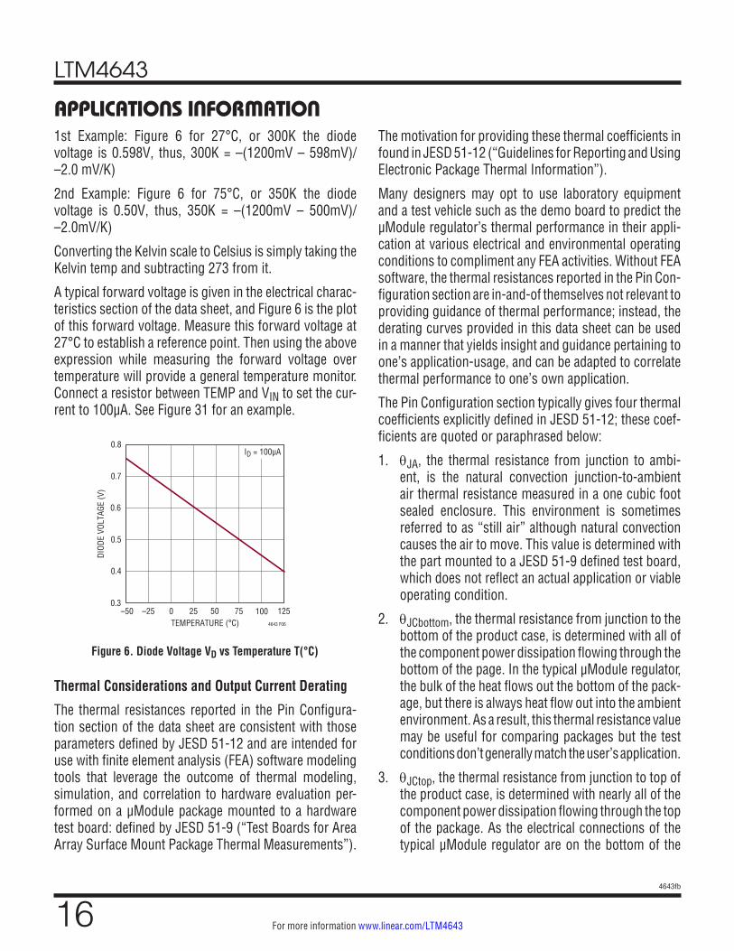
A diode connected PNP transistor is used for the TEMP monitor function by monitoring its voltage over tempera-ture. The temperature dependence of this diode voltage can be understood in the equation:
VD = nVT ln
IDIS
where VT is the thermal voltage (kT/q), and n, the ideality factor, is 1 for the diode connected PNP transistor be-ing used in the LTM4643. IS is expressed by the typical empirical equation:
IS = I0 exp
–VG0
VT
where I0 is a process and geometry dependent current, (I0 is typically around 20k orders of magnitude larger than IS at room temperature) and VG0 is the band gap voltage of 1.2V extrapolated to absolute zero or –273°C.
If we take the IS equation and substitute into the VD equa-tion, then we get:
VD = VG0 –
kTq
ln
I0ID
, VT =
kTq
The expression shows that the diode voltage decreases (linearly if I0 were constant) with increasing temperature and constant diode current. Figure 6 shows a plot of VD vs Temperature over the operating temperature range of the LTM4643.
If we take this equation and differentiate it with respect to temperature T, then:
dVD
dT= –
VG0 – VD
T
This dVD/dT term is the temperature coefficient equal to about –2mV/K or –2mV/°C. The equation is simplified for the first order derivation.
Solving for T, T = –(VG0 – VD)/(dVD/dT) provides the temperature.
LTM4643
164643fb
For more information www.linear.com/LTM4643
APPLICATIONS INFORMATION1st Example: Figure 6 for 27°C, or 300K the diode voltage is 0.598V, thus, 300K = –(1200mV – 598mV)/ –2.0 mV/K)
2nd Example: Figure 6 for 75°C, or 350K the diode voltage is 0.50V, thus, 350K = –(1200mV – 500mV)/ –2.0mV/K)
Converting the Kelvin scale to Celsius is simply taking the Kelvin temp and subtracting 273 from it.
A typical forward voltage is given in the electrical charac-teristics section of the data sheet, and Figure 6 is the plot of this forward voltage. Measure this forward voltage at 27°C to establish a reference point. Then using the above expression while measuring the forward voltage over temperature will provide a general temperature monitor. Connect a resistor between TEMP and VIN to set the cur-rent to 100µA. See Figure 31 for an example.
The motivation for providing these thermal coefficients in found in JESD 51-12 (“Guidelines for Reporting and Using Electronic Package Thermal Information”).
Many designers may opt to use laboratory equipment and a test vehicle such as the demo board to predict the µModule regulator’s thermal performance in their appli-cation at various electrical and environmental operating conditions to compliment any FEA activities. Without FEA software, the thermal resistances reported in the Pin Con-figuration section are in-and-of themselves not relevant to providing guidance of thermal performance; instead, the derating curves provided in this data sheet can be used in a manner that yields insight and guidance pertaining to one’s application-usage, and can be adapted to correlate thermal performance to one’s own application.
The Pin Configuration section typically gives four thermal coefficients explicitly defined in JESD 51-12; these coef-ficients are quoted or paraphrased below:
1. θJA, the thermal resistance from junction to ambi-ent, is the natural convection junction-to-ambient air thermal resistance measured in a one cubic foot sealed enclosure. This environment is sometimes referred to as “still air” although natural convection causes the air to move. This value is determined with the part mounted to a JESD 51-9 defined test board, which does not reflect an actual application or viable operating condition.
2. θJCbottom, the thermal resistance from junction to the bottom of the product case, is determined with all of the component power dissipation flowing through the bottom of the page. In the typical µModule regulator, the bulk of the heat flows out the bottom of the pack-age, but there is always heat flow out into the ambient environment. As a result, this thermal resistance value may be useful for comparing packages but the test conditions don’t generally match the user’s application.
3. θJCtop, the thermal resistance from junction to top of the product case, is determined with nearly all of the component power dissipation flowing through the top of the package. As the electrical connections of the typical µModule regulator are on the bottom of the
Figure 6. Diode Voltage VD vs Temperature T(°C)
TEMPERATURE (°C)–50 –25
0.3
DIOD
E VO
LTAG
E (V
)
0.5
0.8
0 50 75
0.4
0.7
0.6
25 1004643 F06
125
ID = 100µA
Thermal Considerations and Output Current Derating
The thermal resistances reported in the Pin Configura-tion section of the data sheet are consistent with those parameters defined by JESD 51-12 and are intended for use with finite element analysis (FEA) software modeling tools that leverage the outcome of thermal modeling, simulation, and correlation to hardware evaluation per-formed on a µModule package mounted to a hardware test board: defined by JESD 51-9 (“Test Boards for Area Array Surface Mount Package Thermal Measurements”).
LTM4643
174643fb
For more information www.linear.com/LTM4643
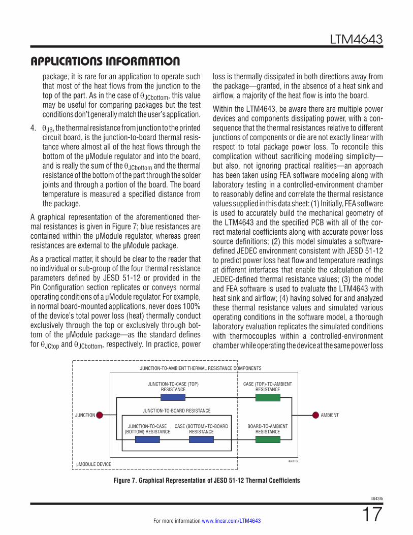
Figure 7. Graphical Representation of JESD 51-12 Thermal Coefficients
4643 F07µMODULE DEVICE
JUNCTION-TO-CASE (TOP)RESISTANCE
JUNCTION-TO-BOARD RESISTANCE
JUNCTION-TO-AMBIENT THERMAL RESISTANCE COMPONENTS
CASE (TOP)-TO-AMBIENTRESISTANCE
BOARD-TO-AMBIENTRESISTANCE
JUNCTION-TO-CASE(BOTTOM) RESISTANCE
JUNCTION AMBIENT
CASE (BOTTOM)-TO-BOARDRESISTANCE
package, it is rare for an application to operate such that most of the heat flows from the junction to the top of the part. As in the case of θJCbottom, this value may be useful for comparing packages but the test conditions don’t generally match the user’s application.
4. θJB, the thermal resistance from junction to the printed circuit board, is the junction-to-board thermal resis-tance where almost all of the heat flows through the bottom of the µModule regulator and into the board, and is really the sum of the θJCbottom and the thermal resistance of the bottom of the part through the solder joints and through a portion of the board. The board temperature is measured a specified distance from the package.
A graphical representation of the aforementioned ther-mal resistances is given in Figure 7; blue resistances are contained within the μModule regulator, whereas green resistances are external to the µModule package.
As a practical matter, it should be clear to the reader that no individual or sub-group of the four thermal resistance parameters defined by JESD 51-12 or provided in the Pin Configuration section replicates or conveys normal operating conditions of a μModule regulator. For example, in normal board-mounted applications, never does 100% of the device’s total power loss (heat) thermally conduct exclusively through the top or exclusively through bot-tom of the µModule package—as the standard defines for θJCtop and θJCbottom, respectively. In practice, power
APPLICATIONS INFORMATIONloss is thermally dissipated in both directions away from the package—granted, in the absence of a heat sink and airflow, a majority of the heat flow is into the board.
Within the LTM4643, be aware there are multiple power devices and components dissipating power, with a con-sequence that the thermal resistances relative to different junctions of components or die are not exactly linear with respect to total package power loss. To reconcile this complication without sacrificing modeling simplicity—but also, not ignoring practical realities—an approach has been taken using FEA software modeling along with laboratory testing in a controlled-environment chamber to reasonably define and correlate the thermal resistance values supplied in this data sheet: (1) Initially, FEA software is used to accurately build the mechanical geometry of the LTM4643 and the specified PCB with all of the cor-rect material coefficients along with accurate power loss source definitions; (2) this model simulates a software-defined JEDEC environment consistent with JESD 51-12 to predict power loss heat flow and temperature readings at different interfaces that enable the calculation of the JEDEC-defined thermal resistance values; (3) the model and FEA software is used to evaluate the LTM4643 with heat sink and airflow; (4) having solved for and analyzed these thermal resistance values and simulated various operating conditions in the software model, a thorough laboratory evaluation replicates the simulated conditions with thermocouples within a controlled-environment chamber while operating the device at the same power loss
LTM4643
184643fb
For more information www.linear.com/LTM4643
as that which was simulated. An outcome of this process and due diligence yields the set of derating curves shown in this data sheet.
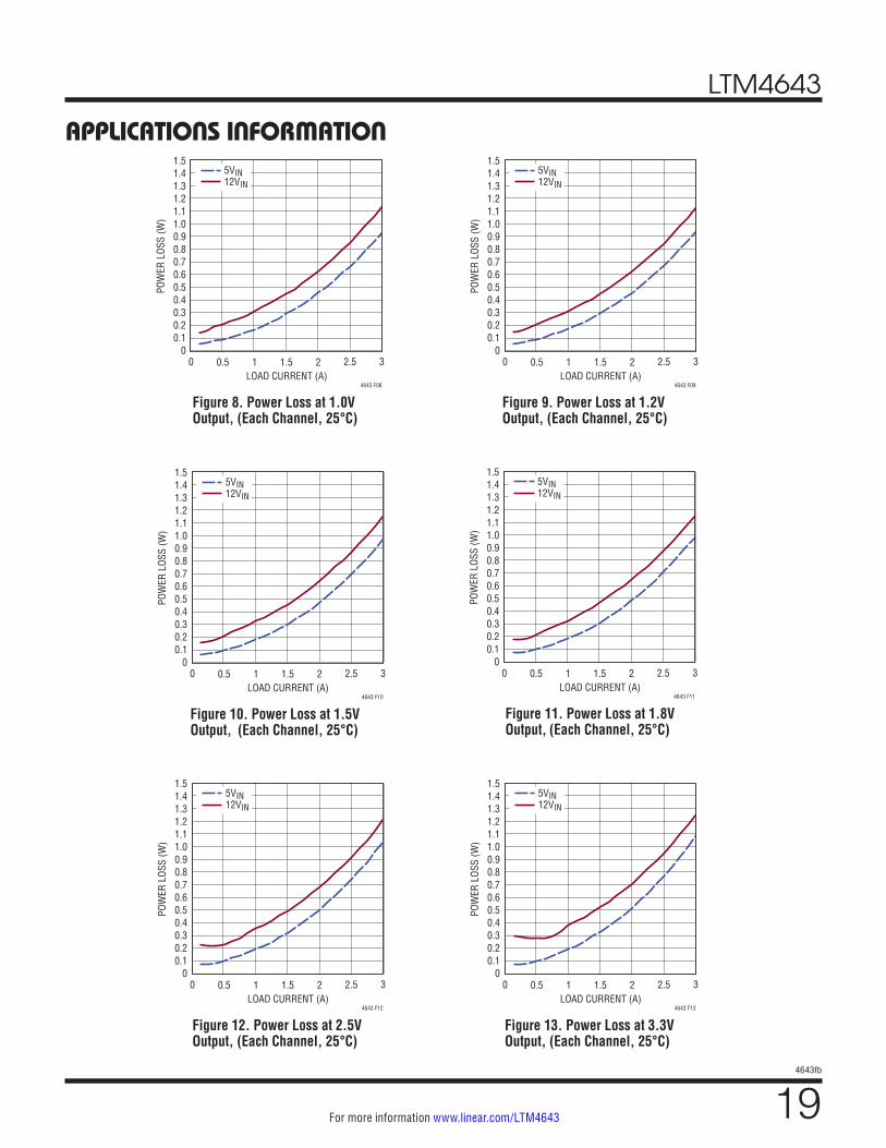
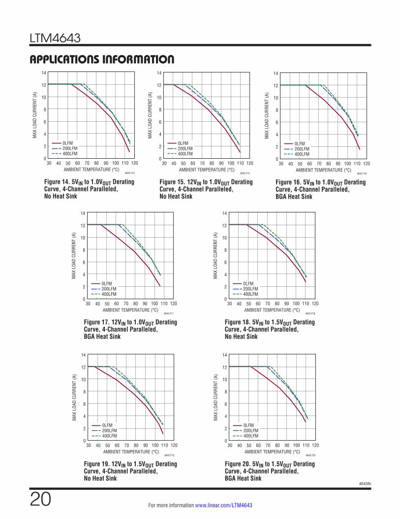
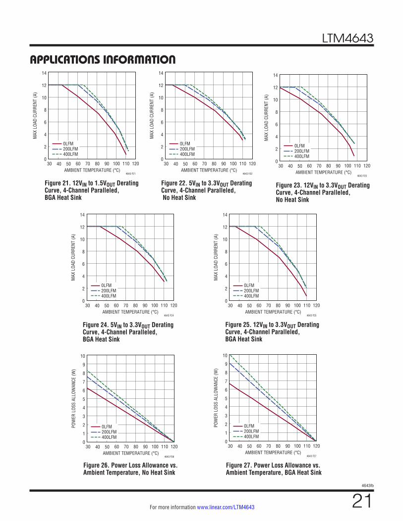
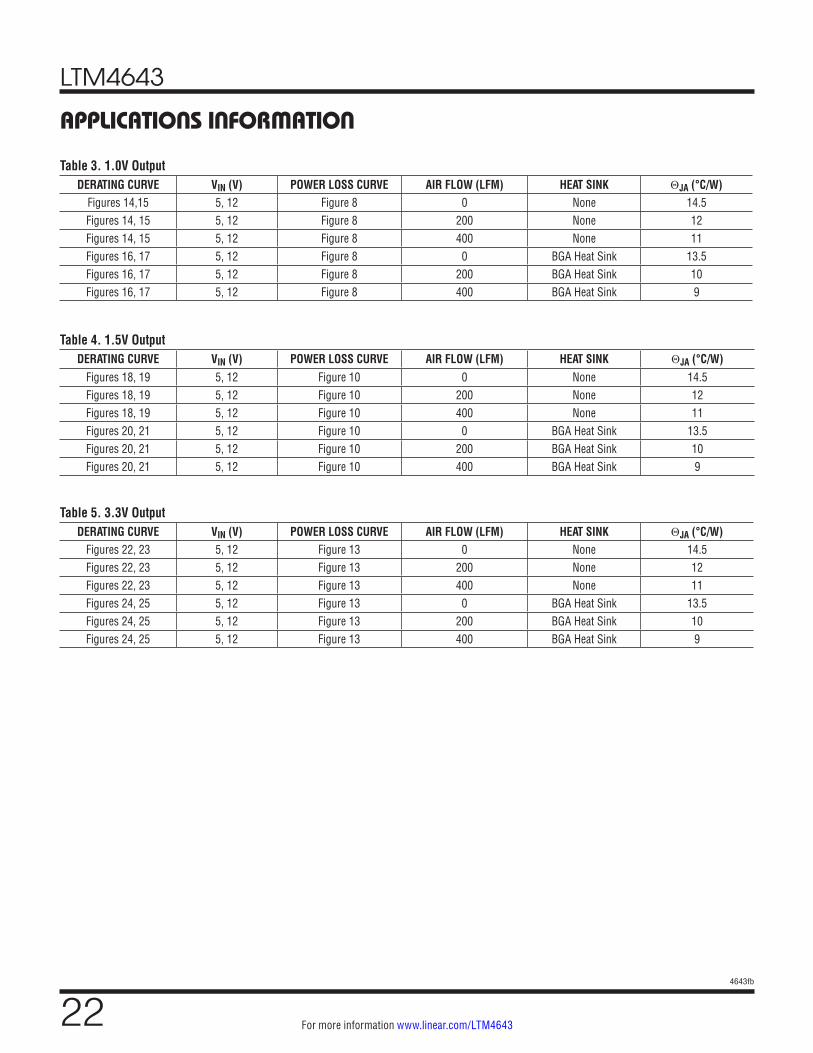
The 1V to 3.3V power loss curves in Figures 8 to 13 can be used in coordination with the load current derating curves in Figures 14 to 25 for calculating an approximate θJA thermal resistance for the LTM4643 with various heat sinking and airflow conditions. The power loss curves are taken at room temperature, and are increased with a multi-plicative factor according to the junction temperature. This approximate factor is 1.3 for 120°C. The derating curves are plotted with the output current starting at 12A and the ambient temperature starting at 30°C. These are chosen to include the lower and higher output voltage ranges for correlating the thermal resistance. Thermal models are derived from several temperature measurements in a controlled temperature chamber along with thermal mod-eling analysis. The junction temperatures are monitored while ambient temperature is increased with and without airflow. The power loss increase with ambient temperature change is factored into the derating curves. The junctions are maintained at 120°C maximum while lowering output current or power with increasing ambient temperature. The decreased output current will decrease the internal module loss as ambient temperature is increased. The monitored junction temperature of 120°C minus the ambient operat-ing temperature specifies how much module temperature rise can be allowed. As an example, in Figure 19 the load current is derated to 10A at ~67°C with 200LFM of airflow and no heat sink and the power loss for the 12V to 1.5V at 10A output is about 4.5W. The 4.5W loss is calculated with 4 times the 0.87W room temperature loss from the 12V to 1.5V power loss curve each channel at 2.5A, and the 1.3 multiplying factor at 120°C junction. If the 67°C ambient temperature is subtracted from the 120°C junction temperature, then the difference of 53°C divided by 4.5W equals 11.7°C/W θJA thermal resistance. Table 3 specifies a 12°C/W value which is very close. Tables 3 to 5 provide equivalent thermal resistances for the different outputs with and without airflow and heat sinking. The derived thermal resistances in Tables 3 to 6 for the various condi-
tions can be multiplied by the calculated power loss as a function of ambient temperature to derive temperature rise above ambient, thus maximum junction temperature. Room temperature power loss can be derived from the efficiency curves in the Typical Performance Characteristics section and adjusted with the above junction temperature multiplicative factor. The printed circuit board is a 1.6mm thick four layer board with two ounce copper for the two outer layers and one ounce copper for the two inner layers. The PCB dimensions are 95mm × 76mm.
The 12A represents all four channels in parallel at 3A each. The four parallel channels have their currents reduced at the same rate to develop an equivalent θJA circuit evalu-ation with thermal couples or IR camera used to validate the thermal resistance values.
Maximum Operating Ambient Temperature
Figures 26 and 27 display the Maximum Power Loss Allowance Curves vs ambient temperature with various heat sinking and airflow conditions. This data was derived from the thermal impedance generated by various ther-mal derating examinations with the junction temperature measured at 120°C. This maximum power loss limitation serves as a guideline when designing multiple output rails with different voltages and currents by calculating the total power loss.
For example, to determine the maximum ambient tem-perature when VOUT1 = 2.5V at 0.6A, VOUT2 = 3.3V at 3A, VOUT3 = 1.8V at 1A, VOUT4 = 1.2V at 3A, without a heat sink and 400LFM airflow, simply add up the total power loss for each channel read from Figure 8 to Figure 13 which in this example equals 3.0W, then multiply by the 1.3 coefficient for 120°C junction temperature and com-pare the total power loss number, 3.9W, with Figure 26. Figure 26 indicates with a 3.9W total power loss, the maximum ambient temperature for this particular ap-plication is around 77°C. Also from Figure 26, it is easy to determine with a 3.4W total power loss, the maximum ambient temperature is around 63°C with no airflow and 73°C with 200LFM airflow.
APPLICATIONS INFORMATION
LTM4643
194643fb
For more information www.linear.com/LTM4643
Figure 8. Power Loss at 1.0V Output, (Each Channel, 25°C)
APPLICATIONS INFORMATION
LOAD CURRENT (A)0
0
POW
ER L
OSS
(W)
0.6
1.51.4
1
4643 F08
0.2
0.4
0.8
1.2
1.0
0.5
1.3
0.1
0.3
0.7
1.1
0.9
320.5 1.5 2.5
5VIN12VIN
LOAD CURRENT (A)0
0
POW
ER L
OSS
(W)
0.6
1.51.4
1
4643 F09
0.2
0.4
0.8
1.2
1.0
0.5
1.3
0.1
0.3
0.7
1.1
0.9
320.5 1.5 2.5
5VIN12VIN
LOAD CURRENT (A)0
0
POW
ER L
OSS
(W)
0.6
1.51.4
1
4643 F10
0.2
0.4
0.8
1.2
1.0
0.5
1.3
0.1
0.3
0.7
1.1
0.9
320.5 1.5 2.5
5VIN12VIN
LOAD CURRENT (A)0
0
POW
ER L
OSS
(W)
0.6
1.51.4
1
4643 F11
0.2
0.4
0.8
1.2
1.0
0.5
1.3
0.1
0.3
0.7
1.1
0.9
320.5 1.5 2.5
5VIN12VIN
LOAD CURRENT (A)0
0
POW
ER L
OSS
(W)
0.6
1.51.4
1
4643 F12
0.2
0.4
0.8
1.2
1.0
0.5
1.3
0.1
0.3
0.7
1.1
0.9
320.5 1.5 2.5
5VIN12VIN
LOAD CURRENT (A)0
0
POW
ER L
OSS
(W)
0.6
1.51.4
1
4643 F13
0.2
0.4
0.8
1.2
1.0
0.5
1.3
0.1
0.3
0.7
1.1
0.9
320.5 1.5 2.5
5VIN12VIN
Figure 9. Power Loss at 1.2V Output, (Each Channel, 25°C)
Figure 10. Power Loss at 1.5V Output, (Each Channel, 25°C)
Figure 11. Power Loss at 1.8V Output, (Each Channel, 25°C)
Figure 12. Power Loss at 2.5V Output, (Each Channel, 25°C)
Figure 13. Power Loss at 3.3V Output, (Each Channel, 25°C)
LTM4643
204643fb
For more information www.linear.com/LTM4643
APPLICATIONS INFORMATION
AMBIENT TEMPERATURE (°C)30
0
10
14
12
4643 F18
4
2
8
6
12040 80 1006050 90 11070
0LFM200LFM400LFM
MAX
LOA
D CU
RREN
T (A
)
AMBIENT TEMPERATURE (°C)30
0
MAX
LOA
D CU
RREN
T (A
)
10
14
12
4643 F19
4
2
8
6
12040 80 1006050 90 11070
0LFM200LFM400LFM
AMBIENT TEMPERATURE (°C)30
0
10
14
12
4643 F16
4
2
8
6
12040 80 1006050 90 11070
0LFM200LFM400LFM
MAX
LOA
D CU
RREN
T (A
)
AMBIENT TEMPERATURE (°C)30
0
10
14
12
4643 F17
4
2
8
6
12040 80 1006050 90 11070
0LFM200LFM400LFM
MAX
LOA
D CU
RREN
T (A
)
AMBIENT TEMPERATURE (°C)30
0
MAX
LOA
D CU
RREN
T (A
)
10
14
12
4643 F20
4
2
8
6
12040 80 1006050 90 11070
0LFM200LFM400LFM
Figure 14. 5VIN to 1.0VOUT Derating Curve, 4-Channel Paralleled, No Heat Sink
AMBIENT TEMPERATURE (°C)30
0
10
14
12
4643 F14
4
2
8
6
12040 80 1006050 90 11070
0LFM200LFM400LFM
MAX
LOA
D CU
RREN
T (A
)
AMBIENT TEMPERATURE (°C)30
0
10
14
12
4643 F15
4
2
8
6
12040 80 1006050 90 11070
0LFM200LFM400LFM
MAX
LOA
D CU
RREN
T (A
)
Figure 15. 12VIN to 1.0VOUT Derating Curve, 4-Channel Paralleled, No Heat Sink
Figure 16. 5VIN to 1.0VOUT Derating Curve, 4-Channel Paralleled, BGA Heat Sink
Figure 17. 12VIN to 1.0VOUT Derating Curve, 4-Channel Paralleled, BGA Heat Sink
Figure 18. 5VIN to 1.5VOUT Derating Curve, 4-Channel Paralleled, No Heat Sink
Figure 19. 12VIN to 1.5VOUT Derating Curve, 4-Channel Paralleled, No Heat Sink
Figure 20. 5VIN to 1.5VOUT Derating Curve, 4-Channel Paralleled, BGA Heat Sink
LTM4643
214643fb
For more information www.linear.com/LTM4643
Figure 21. 12VIN to 1.5VOUT Derating Curve, 4-Channel Paralleled, BGA Heat Sink
Figure 22. 5VIN to 3.3VOUT Derating Curve, 4-Channel Paralleled, No Heat Sink
Figure 23. 12VIN to 3.3VOUT Derating Curve, 4-Channel Paralleled, No Heat Sink
Figure 24. 5VIN to 3.3VOUT Derating Curve, 4-Channel Paralleled, BGA Heat Sink
AMBIENT TEMPERATURE (°C)30
0
MAX
LOA
D CU
RREN
T (A
)
10
14
12
4643 F23
4
2
8
6
12040 80 1006050 90 11070
0LFM200LFM400LFM
AMBIENT TEMPERATURE (°C)30
0
MAX
LOA
D CU
RREN
T (A
)
10
14
12
4643 F22
4
2
8
6
12040 80 1006050 90 11070
0LFM200LFM400LFM
AMBIENT TEMPERATURE (°C)30
0
MAX
LOA
D CU
RREN
T (A
)
10
14
12
4643 F21
4
2
8
6
12040 80 1006050 90 11070
0LFM200LFM400LFM
AMBIENT TEMPERATURE (°C)30
0
MAX
LOA
D CU
RREN
T (A
)
10
14
12
4643 F24
4
2
8
6
12040 80 1006050 90 11070
0LFM200LFM400LFM
APPLICATIONS INFORMATION
Figure 25. 12VIN to 3.3VOUT Derating Curve, 4-Channel Paralleled, BGA Heat Sink
Figure 26. Power Loss Allowance vs. Ambient Temperature, No Heat Sink
Figure 27. Power Loss Allowance vs. Ambient Temperature, BGA Heat Sink
AMBIENT TEMPERATURE (°C)30
0
MAX
LOA
D CU
RREN
T (A
)
10
14
12
4643 F25
4
2
8
6
12040 80 1006050 90 11070
0LFM200LFM400LFM
AMBIENT TEMPERATURE (°C)30
0
POW
ER L
OSS
ALLO
WAN
CE (W
)
8
10
9
4643 F26
4
2
1
5
3
7
6
12040 80 1006050 90 11070
0LFM200LFM400LFM
AMBIENT TEMPERATURE (°C)30
0
POW
ER L
OSS
ALLO
WAN
CE (W
)
8
10
9
4643 F27
4
2
1
5
3
7
6
12040 80 1006050 90 11070
0LFM200LFM400LFM
LTM4643
224643fb
For more information www.linear.com/LTM4643
APPLICATIONS INFORMATION
Table 3. 1.0V OutputDERATING CURVE VIN (V) POWER LOSS CURVE AIR FLOW (LFM) HEAT SINK ΘJA (°C/W)
Figures 14,15 5, 12 Figure 8 0 None 14.5Figures 14, 15 5, 12 Figure 8 200 None 12Figures 14, 15 5, 12 Figure 8 400 None 11Figures 16, 17 5, 12 Figure 8 0 BGA Heat Sink 13.5Figures 16, 17 5, 12 Figure 8 200 BGA Heat Sink 10Figures 16, 17 5, 12 Figure 8 400 BGA Heat Sink 9
Table 4. 1.5V OutputDERATING CURVE VIN (V) POWER LOSS CURVE AIR FLOW (LFM) HEAT SINK ΘJA (°C/W)
Figures 18, 19 5, 12 Figure 10 0 None 14.5Figures 18, 19 5, 12 Figure 10 200 None 12Figures 18, 19 5, 12 Figure 10 400 None 11Figures 20, 21 5, 12 Figure 10 0 BGA Heat Sink 13.5Figures 20, 21 5, 12 Figure 10 200 BGA Heat Sink 10Figures 20, 21 5, 12 Figure 10 400 BGA Heat Sink 9
Table 5. 3.3V OutputDERATING CURVE VIN (V) POWER LOSS CURVE AIR FLOW (LFM) HEAT SINK ΘJA (°C/W)
Figures 22, 23 5, 12 Figure 13 0 None 14.5Figures 22, 23 5, 12 Figure 13 200 None 12Figures 22, 23 5, 12 Figure 13 400 None 11Figures 24, 25 5, 12 Figure 13 0 BGA Heat Sink 13.5Figures 24, 25 5, 12 Figure 13 200 BGA Heat Sink 10Figures 24, 25 5, 12 Figure 13 400 BGA Heat Sink 9
LTM4643
234643fb
For more information www.linear.com/LTM4643
APPLICATIONS INFORMATION
VOUT (V)
CIN (CERAMIC)
(µF)COUT1 (µF)
CFF (pF)
VIN (V)
DROOP (mv)
P-P DERIVATION (mV)
RECOVERY TIME (µs)
LOAD STEP (A)
LOAD STEP SLEW RATE
(A/µs)RFB (kΩ)
CERAMIC ONLY1 10 47 100 5, 12 1 59 40 2A to 3A 0 90.9
1.2 10 47 100 5, 12 1 59 40 2A to 3A 0 60.41.5 10 47 100 5, 12 1 66 40 2A to 3A 0 40.21.8 10 47 100 5, 12 1 75 40 2A to 3A 0 30.12.5 10 47 100 5, 12 2 108 50 2A to 3A 0 19.13.3 10 47 100 5, 12 3 111 60 2A to 3A 0 13.3
POSCAP1 10 100 5, 12 1 89 40 2A to 3A 0 90.9
1.2 10 100 5, 12 1 94 40 2A to 3A 0 60.41.5 10 100 5, 12 1 108 40 2A to 3A 0 40.21.8 10 100 5, 12 1 120 40 2A to 3A 0 30.12.5 10 100 5, 12 2 144 50 2A to 3A 0 19.13.3 10 100 5, 12 3 161 60 2A to 3A 0 13.3
Table 6CIN PART NUMBER VALUE COUT1
(CERAMIC)PART NUMBER VALUE COUT1
(POSCAP)PART NUMBER VALUE
Murata GRM21BR61E106KA73L 10µF, 25V, 0805, X5R
Murata GRM21BR60J476ME15 47µF, 6.3V, 0805, X5R
Sanyo 4TPE100MZB 4V 100µF
Taiyo Yuden TMK212BBJ106KG-T 10µF, 25V, 0805, X5R
Taiyo Yuden JMK212BJ476MG-T 47µF, 6.3V, 0805, X5R
Murata GRM31CR61C226ME15L 22µF, 25V, 1206, X5R
Taiyo Yuden TMK316BBJ226ML-T 22µF, 25V, 1206, X5R
LTM4643
244643fb
For more information www.linear.com/LTM4643
APPLICATIONS INFORMATIONSafety Considerations
The LTM4643 modules do not provide galvanic isolation from VIN to VOUT. There is no internal fuse. If required, a slow blow fuse with a rating twice the maximum input current needs to be provided to protect each unit from catastrophic failure. The device does support thermal shutdown and overcurrent protection.
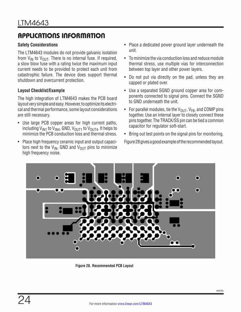
Layout Checklist/Example
The high integration of LTM4643 makes the PCB board layout very simple and easy. However, to optimize its electri-cal and thermal performance, some layout considerations are still necessary.
• Use large PCB copper areas for high current paths, including VIN1 to VIN4, GND, VOUT1 to VOUT4. It helps to minimize the PCB conduction loss and thermal stress.
• Place high frequency ceramic input and output capaci-tors next to the VIN, GND and VOUT pins to minimize high frequency noise.
• Place a dedicated power ground layer underneath the unit.
• To minimize the via conduction loss and reduce module thermal stress, use multiple vias for interconnection between top layer and other power layers.
• Do not put via directly on the pad, unless they are capped or plated over.
• Use a separated SGND ground copper area for com-ponents connected to signal pins. Connect the SGND to GND underneath the unit.
• For parallel modules, tie the VOUT, VFB, and COMP pins together. Use an internal layer to closely connect these pins together. The TRACK/SS pin can be tied a common capacitor for regulator soft-start.
• Bring out test points on the signal pins for monitoring.
Figure 28 gives a good example of the recommended layout.
Figure 28. Recommended PCB Layout
LTM4643
254643fb
For more information www.linear.com/LTM4643
TYPICAL APPLICATIONS
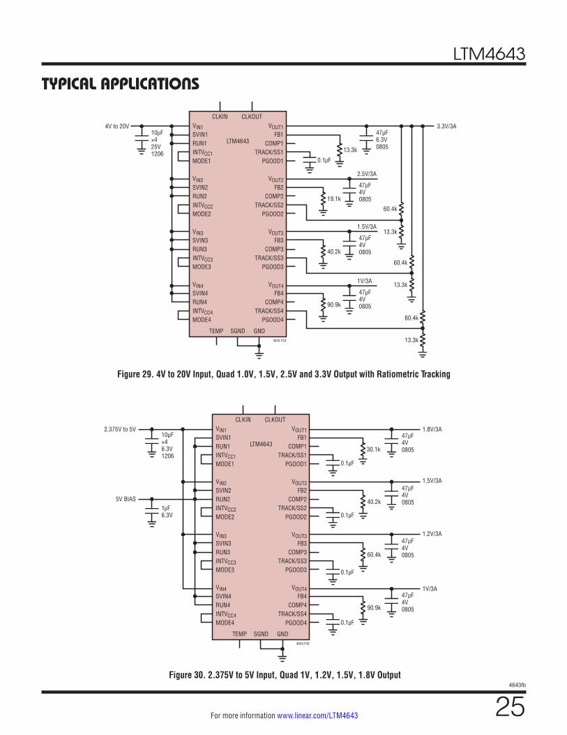
Figure 29. 4V to 20V Input, Quad 1.0V, 1.5V, 2.5V and 3.3V Output with Ratiometric Tracking
4643 F29
VIN1SVIN1RUN1INTVCC1MODE1
VIN2SVIN2RUN2INTVCC2MODE2
VIN3SVIN3RUN3INTVCC3MODE3
VIN4SVIN4RUN4INTVCC4MODE4
SGND
LTM4643
CLKIN
10µF×425V1206
CLKOUT
TEMP GND
VOUT1FB1
COMP1TRACK/SS1
PGOOD1
VOUT2FB2
COMP2TRACK/SS2
PGOOD2
VOUT3FB3
COMP3TRACK/SS3
PGOOD3
VOUT4FB4
COMP4TRACK/SS4
PGOOD4
47µF6.3V0805
3.3V/3A4V to 20V
13.3k
0.1µF
47µF4V0805
2.5V/3A
19.1k
60.4k
13.3k47µF4V0805
1.5V/3A
40.2k
47µF4V0805
1V/3A
90.9k
60.4k
13.3k
60.4k
13.3k
Figure 30. 2.375V to 5V Input, Quad 1V, 1.2V, 1.5V, 1.8V Output
4643 F30
VIN1SVIN1RUN1INTVCC1MODE1
VIN2SVIN2RUN2INTVCC2MODE2
VIN3SVIN3RUN3INTVCC3MODE3
VIN4SVIN4RUN4INTVCC4MODE4
SGND
LTM4643
CLKIN
10µF×46.3V1206
CLKOUT
TEMP GND
VOUT1FB1
COMP1TRACK/SS1
PGOOD1
VOUT2FB2
COMP2TRACK/SS2
PGOOD2
VOUT3FB3
COMP3TRACK/SS3
PGOOD3
VOUT4FB4
COMP4TRACK/SS4
PGOOD4
47µF4V0805
1.8V/3A2.375V to 5V
1µF6.3V
5V BIAS
30.1k
0.1µF
0.1µF
0.1µF
0.1µF
47µF4V0805
1.5V/3A
40.2k
47µF4V0805
1.2V/3A
60.4k
47µF4V0805
1V/3A
90.9k
LTM4643
264643fb
For more information www.linear.com/LTM4643
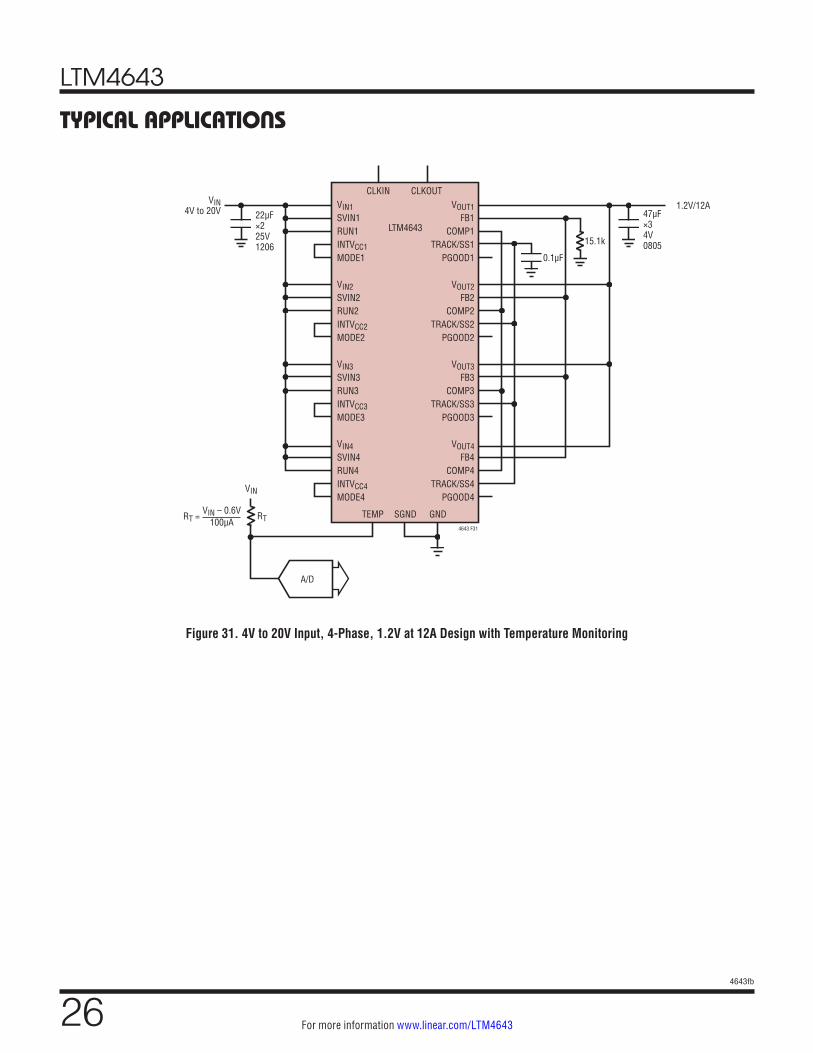
Figure 31. 4V to 20V Input, 4-Phase, 1.2V at 12A Design with Temperature Monitoring
TYPICAL APPLICATIONS
4643 F31
VIN1SVIN1RUN1INTVCC1MODE1
VIN2SVIN2RUN2INTVCC2MODE2
VIN3SVIN3RUN3INTVCC3MODE3
VIN4SVIN4RUN4INTVCC4MODE4
SGND
LTM4643
CLKIN
22µF×225V1206
CLKOUT
TEMP GND
VOUT1FB1
COMP1TRACK/SS1
PGOOD1
VOUT2FB2
COMP2TRACK/SS2
PGOOD2
VOUT3FB3
COMP3TRACK/SS3
PGOOD3
VOUT4FB4
COMP4TRACK/SS4
PGOOD4
47µF×34V0805
1.2V/12AVIN4V to 20V
15.1k
0.1µF
RT
VIN
A/D
RT = VIN – 0.6V
100µA
LTM4643
274643fb
For more information www.linear.com/LTM4643
TYPICAL APPLICATIONS
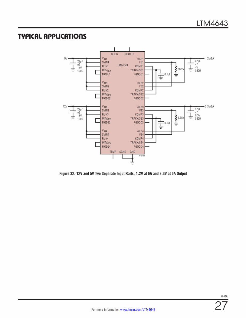
Figure 32. 12V and 5V Two Separate Input Rails, 1.2V at 6A and 3.3V at 6A Output
4643 F32
VIN1SVIN1RUN1INTVCC1MODE1
VIN2SVIN2RUN2INTVCC2MODE2
VIN3SVIN3RUN3INTVCC3MODE3
VIN4SVIN4RUN4INTVCC4MODE4
SGND
LTM4643
CLKIN
22µF×216V1206
CLKOUT
TEMP GND
VOUT1FB1
COMP1TRACK/SS1
PGOOD1
VOUT2FB2
COMP2TRACK/SS2
PGOOD2
VOUT3FB3
COMP3TRACK/SS3
PGOOD3
VOUT4FB4
COMP4TRACK/SS4
PGOOD4
47µF×24V0805
1.2V/6A5V
22µF×216V1206
12V
30.2k
47µF×26.3V0805
3.3V/6A
0.1µF
6.65k
0.1µF
LTM4643
284643fb
For more information www.linear.com/LTM4643
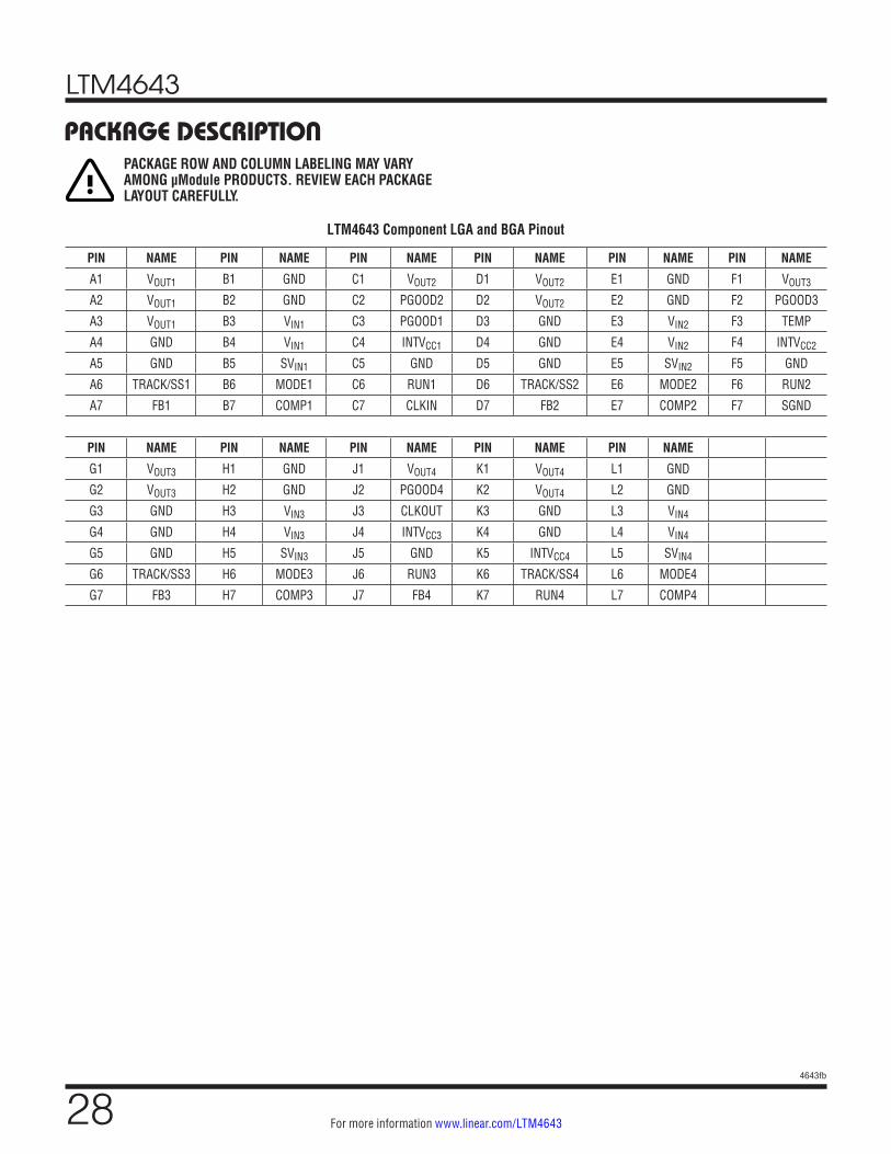
LTM4643 Component LGA and BGA Pinout
PACKAGE DESCRIPTIONPACKAGE ROW AND COLUMN LABELING MAY VARY AMONG µModule PRODUCTS. REVIEW EACH PACKAGE LAYOUT CAREFULLY.
PIN NAME PIN NAME PIN NAME PIN NAME PIN NAME PIN NAME
A1 VOUT1 B1 GND C1 VOUT2 D1 VOUT2 E1 GND F1 VOUT3
A2 VOUT1 B2 GND C2 PGOOD2 D2 VOUT2 E2 GND F2 PGOOD3
A3 VOUT1 B3 VIN1 C3 PGOOD1 D3 GND E3 VIN2 F3 TEMP
A4 GND B4 VIN1 C4 INTVCC1 D4 GND E4 VIN2 F4 INTVCC2
A5 GND B5 SVIN1 C5 GND D5 GND E5 SVIN2 F5 GND
A6 TRACK/SS1 B6 MODE1 C6 RUN1 D6 TRACK/SS2 E6 MODE2 F6 RUN2
A7 FB1 B7 COMP1 C7 CLKIN D7 FB2 E7 COMP2 F7 SGND
PIN NAME PIN NAME PIN NAME PIN NAME PIN NAME
G1 VOUT3 H1 GND J1 VOUT4 K1 VOUT4 L1 GND
G2 VOUT3 H2 GND J2 PGOOD4 K2 VOUT4 L2 GND
G3 GND H3 VIN3 J3 CLKOUT K3 GND L3 VIN4
G4 GND H4 VIN3 J4 INTVCC3 K4 GND L4 VIN4
G5 GND H5 SVIN3 J5 GND K5 INTVCC4 L5 SVIN4
G6 TRACK/SS3 H6 MODE3 J6 RUN3 K6 TRACK/SS4 L6 MODE4
G7 FB3 H7 COMP3 J7 FB4 K7 RUN4 L7 COMP4
LTM4643
294643fb
For more information www.linear.com/LTM4643
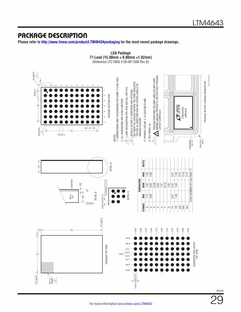
PACKAGE DESCRIPTIONPlease refer to http://www.linear.com/product/LTM4643#packaging for the most recent package drawings.
LGA Package77-Lead (15.00mm × 9.00mm ×1.82mm)
(Reference LTC DWG # 05-08-1508 Rev Ø)
PACK
AGE
TOP
VIEW
4
PIN
“A1”
CORN
ER
YX
aaa
Z
aaa
Z
LGA
Pack
age
77-L
ead
(15.
00m
m ×
9.0
0mm
× 1
.82m
m)
(Ref
eren
ce L
TC D
WG#
05-
08-1
508
Rev
Ø)
D
E
LGA
77 0
715
REV
Ø
TRAY
PIN
1BE
VEL
PACK
AGE
IN T
RAY
LOAD
ING
ORIE
NTAT
ION
COM
PONE
NTPI
N “A
1”
LTM
XXXX
XXµM
odul
e
DETA
IL A
PACK
AGE
BOTT
OM V
IEW
3
SEE
NOTE
S
A B C D E F G H J K L
PIN
1
e
b
F
G
76
54
32
1
SUGG
ESTE
D PC
B LA
YOUT
TOP
VIEW
0.00
0
2.54
0
3.81
0
5.08
0
6.35
0
1.27
0
3.81
0
2.54
0
1.27
0
5.08
0
6.35
0
3.810
2.540
1.270
3.810
2.540
1.270
0.3175
0.31750.000
0.63
0 ±0
.025
Ø 7
7x
7
SEE
NOTE
S
DETA
IL B
DETA
IL B
SUBS
TRAT
EM
OLD
CAP
// bbb Z
Z
A
SYM
BOL
A b D E e F G H1 H2 aaa
bbb
eee
MIN
1.72
0.60
0.27
1.45
NOM
1.82
0.63
15.0
09.
001.
2712
.70
7.62
0.32
1.50
MAX
1.92
0.66
0.37
1.55
0.15
0.10
0.15
NOTE
S
DIM
ENSI
ONS
TOTA
L NU
MBE
R OF
LGA
PAD
S: 7
7
H2H1
0.63
0 ±0
.025
Ø 7
7x
SY
XZ
Ø ee
e
DETA
IL A
NOTE
S:1.
DIM
ENSI
ONIN
G AN
D TO
LERA
NCIN
G PE
R AS
ME
Y14.
5M-1
994
2. A
LL D
IMEN
SION
S AR
E IN
MIL
LIM
ETER
S
LAN
D DE
SIGN
ATIO
N PE
R JE
SD M
O-22
2, S
PP-0
10
5. P
RIM
ARY
DATU
M -Z
- IS
SEAT
ING
PLAN
E
6. P
AD F
INIS
H: A
u
43
DETA
ILS
OF P
AD #
1 ID
ENTI
FIER
ARE
OPT
IONA
L,BU
T M
UST
BE L
OCAT
ED W
ITHI
N TH
E ZO
NE IN
DICA
TED.
THE
PAD
#1 ID
ENTI
FIER
MAY
BE
EITH
ER A
MOL
D OR
M
ARKE
D FE
ATUR
E
7PA
CKAG
E RO
W A
ND C
OLUM
N LA
BELI
NG M
AY V
ARY
AMON
G µM
odul
e PR
ODUC
TS. R
EVIE
W E
ACH
PACK
AGE
LAYO
UT C
AREF
ULLY
!
LTM4643
304643fb
For more information www.linear.com/LTM4643
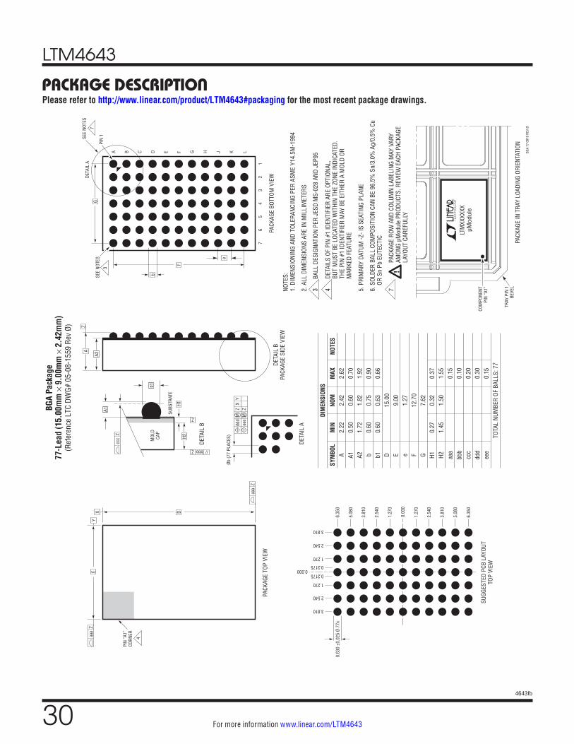
PACKAGE DESCRIPTIONPlease refer to http://www.linear.com/product/LTM4643#packaging for the most recent package drawings.
PACK
AGE
TOP
VIEW
4
PIN
“A1”
CORN
ER
YX
aaa
Z
aaa
Z
BGA
Pack
age
77-L
ead
(15.
00m
m ×
9.0
0mm
× 2
.42m
m)
(Ref
eren
ce L
TC D
WG#
05-
08-1
559
Rev
Ø)
NOTE
S:1.
DIM
ENSI
ONIN
G AN
D TO
LERA
NCIN
G PE
R AS
ME
Y14.
5M-1
994
2. A
LL D
IMEN
SION
S AR
E IN
MIL
LIM
ETER
S
BAL
L DE
SIGN
ATIO
N PE
R JE
SD M
S-02
8 AN
D JE
P95
5. P
RIM
ARY
DATU
M -Z
- IS
SEAT
ING
PLAN
E
6. S
OLDE
R BA
LL C
OMPO
SITI
ON C
AN B
E 96
.5%
Sn/
3.0%
Ag/
0.5%
Cu
OR
Sn
Pb E
UTEC
TIC
43
DETA
ILS
OF P
IN #
1 ID
ENTI
FIER
ARE
OPT
IONA
L,BU
T M
UST
BE L
OCAT
ED W
ITHI
N TH
E ZO
NE IN
DICA
TED.
THE
PIN
#1 ID
ENTI
FIER
MAY
BE
EITH
ER A
MOL
D OR
M
ARKE
D FE
ATUR
E
DETA
IL A
Øb (7
7 PL
ACES
)
DETA
IL B
SUBS
TRAT
E
A
A1
b1
ccc
Z
DETA
IL B
PACK
AGE
SIDE
VIE
W
MOL
DCA
P
Z
MX
YZ
ddd
MZ
eee
SYM
BOL
A A1 A2 b b1 D E e F G H1 H2 aaa
bbb
ccc
ddd
eee
MIN
2.22
0.50
1.72
0.60
0.60
0.27
1.45
NOM
2.42
0.60
1.82
0.75
0.63
15.0
09.
001.
2712
.70
7.62
0.32
1.50
MAX
2.62
0.70
1.92
0.90
0.66
0.37
1.55
0.15
0.10
0.20
0.30
0.15
NOTE
S
DIM
ENSI
ONS
TOTA
L NU
MBE
R OF
BAL
LS: 7
7
A2
D
E
// bbb Z
Z
H2H1
BGA
77 0
916
REV
Ø
TRAY
PIN
1BE
VEL
PACK
AGE
IN T
RAY
LOAD
ING
ORIE
NTAT
ION
COM
PONE
NTPI
N “A
1”
LTM
XXXX
XXµM
odul
e
DETA
IL A
PACK
AGE
BOTT
OM V
IEW
3
SEE
NOTE
S
A B C D E F G H J K L
PIN
1
e
b
F
G
76
54
32
1
SUGG
ESTE
D PC
B LA
YOUT
TOP
VIEW
0.00
0
2.54
0
3.81
0
5.08
0
6.35
0
1.27
0
3.81
0
2.54
0
1.27
0
5.08
0
6.35
0
3.810
2.540
1.270
3.810
2.540
1.270
0.3175
0.31750.000
0.63
0 ±0
.025
Ø 7
7x
7PA
CKAG
E RO
W A
ND C
OLUM
N LA
BELI
NG M
AY V
ARY
AMON
G µM
odul
e PR
ODUC
TS. R
EVIE
W E
ACH
PACK
AGE
LAYO
UT C
AREF
ULLY
!
7
SEE
NOTE
S
LTM4643
314643fb
For more information www.linear.com/LTM4643
Information furnished by Linear Technology Corporation is believed to be accurate and reliable. However, no responsibility is assumed for its use. Linear Technology Corporation makes no representa-tion that the interconnection of its circuits as described herein will not infringe on existing patent rights.
REVISION HISTORYREV DATE DESCRIPTION PAGE NUMBER
A 03/17 Added the BGA package 1, 2, 28, 30
B 6/17 Corrected Output Current from 4A to 3A on Figure 4Corrected Output Voltage from 1.2V to 1.0V on Title of Figure 29
1325
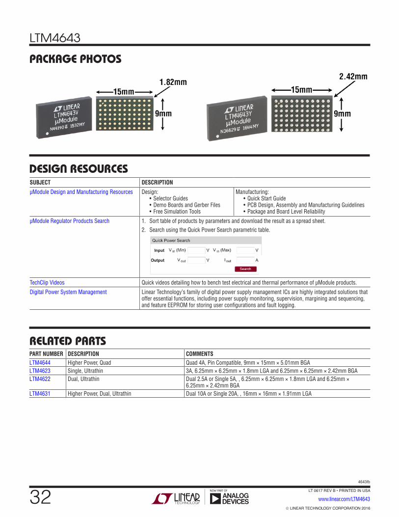
LTM4643
324643fb
For more information www.linear.com/LTM4643 LINEAR TECHNOLOGY CORPORATION 2016
LT 0617 REV B • PRINTED IN USA
www.linear.com/LTM4643
SUBJECT DESCRIPTION
µModule Design and Manufacturing Resources Design: • Selector Guides • Demo Boards and Gerber Files • Free Simulation Tools
Manufacturing: • Quick Start Guide • PCB Design, Assembly and Manufacturing Guidelines • Package and Board Level Reliability
µModule Regulator Products Search 1. Sort table of products by parameters and download the result as a spread sheet.2. Search using the Quick Power Search parametric table.
TechClip Videos Quick videos detailing how to bench test electrical and thermal performance of µModule products.
Digital Power System Management Linear Technology’s family of digital power supply management ICs are highly integrated solutions that offer essential functions, including power supply monitoring, supervision, margining and sequencing, and feature EEPROM for storing user configurations and fault logging.
PACKAGE PHOTOS
RELATED PARTSPART NUMBER DESCRIPTION COMMENTSLTM4644 Higher Power, Quad Quad 4A, Pin Compatible, 9mm × 15mm × 5.01mm BGALTM4623 Single, Ultrathin 3A, 6.25mm × 6.25mm × 1.8mm LGA and 6.25mm × 6.25mm × 2.42mm BGALTM4622 Dual, Ultrathin Dual 2.5A or Single 5A, , 6.25mm × 6.25mm × 1.8mm LGA and 6.25mm ×
6.25mm × 2.42mm BGALTM4631 Higher Power, Dual, Ultrathin Dual 10A or Single 20A, , 16mm × 16mm × 1.91mm LGA
DESIGN RESOURCES