ltm4638 20vin, 15a step-down dc/dc µmodule regulator › media › en › technical-documentation...
TRANSCRIPT
LTM4638
1Rev. B
For more information www.analog.com
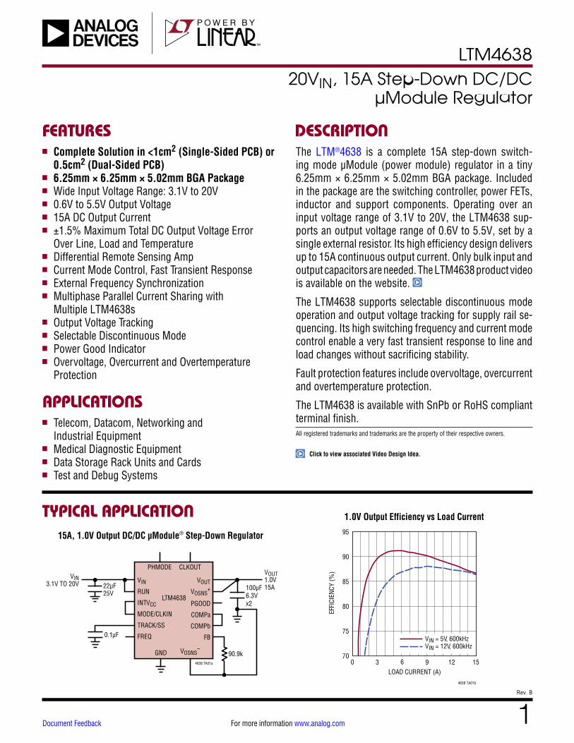
TYPICAL APPLICATION
FEATURES DESCRIPTION
20VIN, 15A Step-Down DC/DC µModule Regulator
The LTM®4638 is a complete 15A step-down switch-ing mode µModule (power module) regulator in a tiny 6.25mm × 6.25mm × 5.02mm BGA package. Included in the package are the switching controller, power FETs, inductor and support components. Operating over an input voltage range of 3.1V to 20V, the LTM4638 sup-ports an output voltage range of 0.6V to 5.5V, set by a single external resistor. Its high efficiency design delivers up to 15A continuous output current. Only bulk input and output capacitors are needed. The LTM4638 product video is available on the website.
The LTM4638 supports selectable discontinuous mode operation and output voltage tracking for supply rail se-quencing. Its high switching frequency and current mode control enable a very fast transient response to line and load changes without sacrificing stability.
Fault protection features include overvoltage, overcurrent and overtemperature protection.
The LTM4638 is available with SnPb or RoHS compliant terminal finish.
15A, 1.0V Output DC/DC µModule® Step-Down Regulator
1.0V Output Efficiency vs Load Current
APPLICATIONS
n Complete Solution in <1cm2 (Single-Sided PCB) or 0.5cm2 (Dual-Sided PCB)
n 6.25mm × 6.25mm × 5.02mm BGA Package n Wide Input Voltage Range: 3.1V to 20V n 0.6V to 5.5V Output Voltage n 15A DC Output Current n ±1.5% Maximum Total DC Output Voltage Error
Over Line, Load and Temperature n Differential Remote Sensing Amp n Current Mode Control, Fast Transient Response n External Frequency Synchronization n Multiphase Parallel Current Sharing with
Multiple LTM4638s n Output Voltage Tracking n Selectable Discontinuous Mode n Power Good Indicator n Overvoltage, Overcurrent and Overtemperature
Protection
n Telecom, Datacom, Networking and Industrial Equipment
n Medical Diagnostic Equipment n Data Storage Rack Units and Cards n Test and Debug Systems
All registered trademarks and trademarks are the property of their respective owners.
90.9k4638 TA01a
22µF25V
VIN3.1V TO 20V
VOUT1.0V15A100µF
6.3Vx2
0.1µF
VIN
RUN
INTVCC
MODE/CLKIN
TRACK/SS
FREQ
VOUT
VOSNS+
PHMODE CLKOUT
PGOOD
COMPa
COMPb
FB
GND
LTM4638
VOSNS–
LOAD CURRENT (A)0
EFFI
CIEN
CY (%
)
80
85
90
15
4638 TA01b
75
3 6 9 1270
95
VIN = 5V, 600kHzVIN = 12V, 600kHz
Document Feedback
Click to view associated Video Design Idea.
LTM4638
2Rev. B
For more information www.analog.com
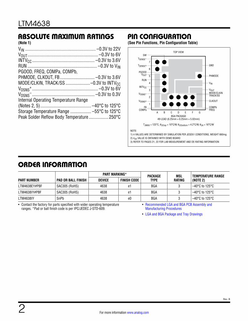
PIN CONFIGURATIONABSOLUTE MAXIMUM RATINGS
VIN ............................................................. –0.3V to 22VVOUT ............................................................. –0.3V to 6VINTVCC ...................................................... –0.3V to 3.6VRUN ............................................................ –0.3V to VIN PGOOD, FREQ, COMPa, COMPb,PHMODE, CLKOUT, FB .............................. –0.3V to 3.6VMODE/CLKIN, TRACK/SS .....................–0.3V to INTVCCVOSNS
+ ......................................................... –0.3V to 6VVOSNS
– ...................................................... –0.3V to 0.3VInternal Operating Temperature Range(Notes 2, 5) ............................................ –40°C to 125°CStorage Temperature Range .................. –55°C to 125°CPeak Solder Reflow Body Temperature ................. 250°C
(Note 1) (See Pin Functions, Pin Configuration Table)
BGA PACKAGE49-LEAD (6.25mm × 6.25mm × 5.02mm)
TJMAX = 125°C, θJCtop = 10°C/W, θJCbottom = 4.2°C/W, θJA = 16°C/W
TOP VIEW
5
1
2
3
4
7
6
A B C D E F G
NOTE:1) θ VALUES ARE DETERMINED BY SIMULATION PER JESD51 CONDITIONS, WEIGHT 660mg2) θJA VALUE IS OBTAINED WITH DEMO BOARD3) REFER TO PAGES 21, 22 FOR LAB MEASUREMENT AND DE-RATING INFORMATION
VOUT
VIN
PHMODE
GND
TSENSE–
TSENSE+
SW
CLKOUT
COMPbFREQ
VOSNS– MODE/CLKINTRACK/SS
VOSNS+
INTVCC
RUN
PGOOD
FBCOMPa
VOUT
ORDER INFORMATION
PART NUMBER PAD OR BALL FINISH
PART MARKING* PACKAGE TYPE
MSL RATING
TEMPERATURE RANGE (NOTE 2)DEVICE FINISH CODE
LTM4638EY#PBF SAC305 (RoHS) 4638 e1 BGA 3 –40°C to 125°C
LTM4638IY#PBF SAC305 (RoHS) 4638 e1 BGA 3 –40°C to 125°C
LTM4638IY SnPb 4638 e0 BGA 3 –40°C to 125°C
• Contact the factory for parts specified with wider operating temperature ranges. *Pad or ball finish code is per IPC/JEDEC J-STD-609.
• Recommended LGA and BGA PCB Assembly and Manufacturing Procedures
• LGA and BGA Package and Tray Drawings
LTM4638
3Rev. B
For more information www.analog.com
ELECTRICAL CHARACTERISTICS The l denotes the specifications which apply over the specified internal operating temperature range (Note 2), otherwise specifications are at TA = 25°C. VIN = 12V per the typical application shown on the front page.
SYMBOL PARAMETER CONDITIONS MIN TYP MAX UNITS
Switching Regulator Section: per Channel
VIN Input DC Voltage l 3.1 20 V
VOUT Output Voltage Range l 0.6 5.5 V
VOUT(DC) Output Voltage, Total Variation with Line and Load (Note 6)
CIN = 22µF, COUT = 100µF Ceramic, RFB = 40.2k, MODE = INTVCC, IOUT = 0A to 15A (Note 3) –40°C to 125°C
l
1.477
1.50
1.523
V
VRUN RUN Pin On Threshold VRUN Rising 1.1 1.25 1.35 V
IQ(VIN) Input Supply Bias Current VIN = 12V, VOUT = 1.5V, MODE = INTVCC VIN = 12V, VOUT = 1.5V, MODE = GND Shutdown, RUN = 0, VIN = 12V
100 18 20
mA mA µA
IS(VIN) Input Supply Current VIN = 12V, VOUT = 1.5V, IOUT = 15A 2.3 A
IOUT(DC) Output Continuous Current Range
VIN = 12V, VOUT = 1.5V 0 15 A
ΔVOUT (Line)/VOUT Line Regulation Accuracy VOUT = 1.5V, VIN = 3.1V to 20V, IOUT = 0A l 0.04 0.15 %/V
ΔVOUT (Load)/VOUT Load Regulation Accuracy VOUT = 1.5V, IOUT = 0A to 15A l 0.5 1.2 %
VOUT(AC) Output Ripple Voltage IOUT = 0A, COUT = 100µF Ceramic, VIN = 12V, VOUT = 1.5V
5 mV
ΔVOUT(START) Turn-On Overshoot IOUT = 0A, COUT = 100µF Ceramic, VIN = 12V, VOUT = 1.5V
30 mV
tSTART Turn-On Time COUT = 100µF Ceramic, No Load, TRACK/SS = 0.01µF, VIN = 12V, VOUT = 1.5V
2.5 ms
ΔVOUTLS Peak Deviation for Dynamic Load
Load: 0% to 50% to 0% of Full Load, COUT = 47µF Ceramic, VIN = 12V, VOUT = 1.5V
160 mV
tSETTLE Settling Time for Dynamic Load Step
Load: 0% to 50% to 0% of Full Load, COUT = 47µF Ceramic, VIN = 12V, VOUT = 1.5V
40 µs
IOUTPK Output Current Limit VIN = 12V, VOUT = 1.5V 18 A
VFB Voltage at FB Pin IOUT = 0A, VOUT = 1.5V l 0.594 0.60 0.606 V
IFB Current at FB Pin (Note 4) ±30 nA
RFBHI Resistor Between VOUT and FB Pins
60.05 60.40 60.75 kΩ
ITRACK/SS Track Pin Soft-Start Pull-Up Current
TRACK/SS = 0V 6 10 µA
VIN(UVLO) VIN Undervoltage Lockout VIN Falling VIN Hysteresis
2.5 2.6 250
2.7 V mV
tON(MIN) Minimum On-Time (Note 4) 25 ns
tOFF(MIN) Minimum Off-Time (Note 4) 50 ns
VPGOOD PGOOD Trip Level VFB With Respect to Set Output VFB Ramping Negative VFB Ramping Positive
–12 5
–8 8
–5 12
% %
IPGOOD PGOOD Leakage 2 µA
VPGL PGOOD Voltage Low IPGOOD = 1mA 0.02 0.1 V
LTM4638
4Rev. B
For more information www.analog.com
Note 1: Stresses beyond those listed under Absolute Maximum Ratings may cause permanent damage to the device. Exposure to any Absolute Maximum Rating condition for extended periods may affect device reliability and lifetime.Note 2: The LTM4638 is tested under pulsed load conditions such that TJ ≈ TA. The LTM4638E is guaranteed to meet performance specifications over the 0°C to 125°C internal operating temperature range. Specifications over the –40°C to 125°C internal operating temperature range are assured by design, characterization and correlation with statistical process controls. The LTM4638I is guaranteed to meet specifications over the full –40°C to 125°C internal operating temperature range. Note that the
maximum ambient temperature consistent with these specifications is determined by specific operating conditions in conjunction with board layout, the rated package thermal resistance and other environmental factors.Note 3: See output current derating curves for different VIN, VOUT and TA.Note 4: 100% tested at wafer level.Note 5: This IC includes overtemperature protection that is intended to protect the device during momentary overload conditions. Junction temperature will exceed 125°C when overtemperature protection is active. Continuous operation above the specified maximum operating junction temperature may impair device reliability.
ELECTRICAL CHARACTERISTICS
SYMBOL PARAMETER CONDITIONS MIN TYP MAX UNITS
VINTVCC Internal VCC Voltage VIN = 4V to 20V 3.2 3.3 3.4 V
fOSC Oscillator Frequency 600 kHz
The l denotes the specifications which apply over the specified internal operating temperature range (Note 2), otherwise specifications are at TA = 25°C. VIN = 12V per the typical application shown on the front page.
LTM4638
5Rev. B
For more information www.analog.com
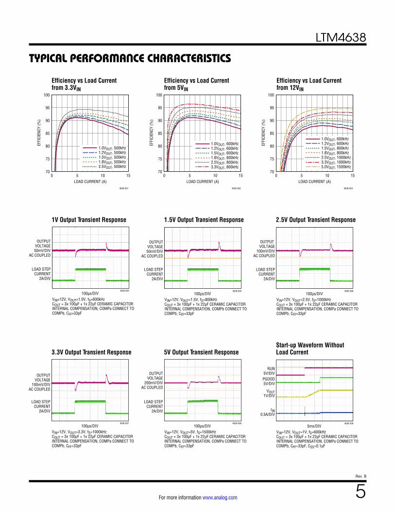
TYPICAL PERFORMANCE CHARACTERISTICS
1V Output Transient Response
3.3V Output Transient Response
1.5V Output Transient Response
5V Output Transient ResponseStart-up Waveform Without Load Current
2.5V Output Transient Response
Efficiency vs Load Current from 3.3VIN
Efficiency vs Load Current from 5VIN
Efficiency vs Load Current from 12VIN
LOAD CURRENT (A)0
EFFI
CIEN
CY (%
)
80
85
90
15
4638 G01
75
5 1070
100
95
1.0VOUT, 500kHz1.2VOUT, 500kHz1.5VOUT, 500kHz1.8VOUT, 500kHz2.5VOUT, 500kHz
LOAD CURRENT (A)0
EFFI
CIEN
CY (%
)80
85
90
15
4638 G02
75
5 1070
100
95
1.0VOUT, 600kHz1.2VOUT, 600kHz1.5VOUT, 600kHz1.8VOUT, 800kHz2.5VOUT, 800kHz3.3VOUT, 800kHz
LOAD CURRENT (A)0
EFFI
CIEN
CY (%
)
80
85
90
15
4638 G03
75
5 1070
100
95
1.0VOUT, 600kHz1.2VOUT, 600kHz1.5VOUT, 800kHz1.8VOUT, 800kHz2.5VOUT, 1000kHz3.3VOUT, 1000kHz5.0VOUT, 1500kHz
100µs/DIV
OUTPUTVOLTAGE50mV/DIV
AC COUPLED
LOAD STEPCURRENT
2A/DIV
4638 G04
VIN=12V, VOUT=1.0V, fS=600kHzCOUT = 3x 100µF + 1x 22µF CERAMIC CAPACITORINTERNAL COMPENSATION, COMPa CONNECT TOCOMPb, CFF=33pF
100µs/DIV
OUTPUTVOLTAGE50mV/DIV
AC COUPLED
LOAD STEPCURRENT
2A/DIV
4638 G05
VIN=12V, VOUT=1.5V, fS=800kHzCOUT = 3x 100µF + 1x 22µF CERAMIC CAPACITORINTERNAL COMPENSATION, COMPb CONNECT TOCOMPb, CFF=33pF
100µs/DIV
OUTPUT VOLTAGE
100mV/DIVAC COUPLED
LOAD STEPCURRENT
2A/DIV
4638 G06
VIN=12V, VOUT=2.5V, fS=1000kHzCOUT = 3x 100µF + 1x 22µF CERAMIC CAPACITORINTERNAL COMPENSATION, COMPa CONNECT TOCOMPb, CFF=33pF
100µs/DIV
OUTPUTVOLTAGE
100mV/DIVAC COUPLED
LOAD STEPCURRENT
2A/DIV
4638 G07
VIN=12V, VOUT=3.3V, fS=1000kHzCOUT = 3x 100µF + 1x 22µF CERAMIC CAPACITORINTERNAL COMPENSATION, COMPa CONNECT TOCOMPb, CFF=33pF
100µs/DIV
OUTPUTVOLTAGE
200mV/DIVAC COUPLED
LOAD STEPCURRENT
2A/DIV
4638 G08
VIN=12V, VOUT=5V, fS=1500kHzCOUT = 3x 100µF + 1x 22µF CERAMIC CAPACITORINTERNAL COMPENSATION, COMPa CONNECT TOCOMPb, CFF=33pF
5ms/DIV
RUN5V/DIVPGOOD5V/DIV
VOUT1V/DIV
IIN0.5A/DIV
4638 G09
VIN=12V, VOUT=1V, fS=600kHzCOUT = 3x 100µF + 1x 22µF CERAMIC CAPACITORINTERNAL COMPENSATION, COMPa CONNECT TOCOMPb, CFF=33pF, CSS=0.1µF
LTM4638
6Rev. B
For more information www.analog.com
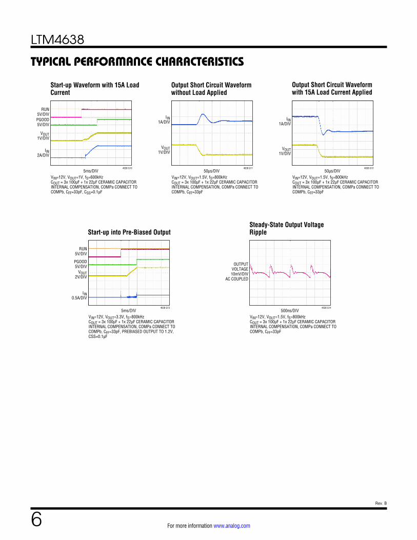
Start-up Waveform with 15A Load Current
Output Short Circuit Waveform with 15A Load Current Applied
Output Short Circuit Waveform without Load Applied
Start-up into Pre-Biased OutputSteady-State Output Voltage Ripple
TYPICAL PERFORMANCE CHARACTERISTICS
5ms/DIV
RUN5V/DIVPGOOD5V/DIV
VOUT1V/DIV
IIN2A/DIV
4638 G10
VIN=12V, VOUT=1V, fS=600kHzCOUT = 3x 100µF + 1x 22µF CERAMIC CAPACITORINTERNAL COMPENSATION, COMPa CONNECT TOCOMPb, CFF=33pF, CSS=0.1µF
50µs/DIV
VOUT1V/DIV
IIN1A/DIV
4638 G11
VIN=12V, VOUT=1.5V, fS=800kHzCOUT = 3x 100µF + 1x 22µF CERAMIC CAPACITORINTERNAL COMPENSATION, COMPa CONNECT TOCOMPb, CFF=33pF
50µs/DIV
VOUT1V/DIV
IIN1A/DIV
4638 G12
VIN=12V, VOUT=1.5V, fS=800kHzCOUT = 3x 100µF + 1x 22µF CERAMIC CAPACITORINTERNAL COMPENSATION, COMPa CONNECT TOCOMPb, CFF=33pF
5ms/DIV
VOUT2V/DIV
IIN0.5A/DIV
RUN5V/DIV
PGOOD5V/DIV
4638 G13
VIN=12V, VOUT=3.3V, fS=800kHzCOUT = 3x 100µF + 1x 22µF CERAMIC CAPACITORINTERNAL COMPENSATION, COMPa CONNECT TOCOMPb, CFF=33pF, PREBIASED OUTPUT TO 1.2V, CSS=0.1µF
500ns/DIV
OUTPUTVOLTAGE10mV/DIV
AC COUPLED
4638 G14
VIN=12V, VOUT=1.5V, fS=800kHzCOUT = 3x 100µF + 1x 22µF CERAMIC CAPACITORINTERNAL COMPENSATION, COMPa CONNECT TOCOMPb, CFF=33pF
LTM4638
7Rev. B
For more information www.analog.com
PIN FUNCTIONS
VOUT (A1-A5, F3, G1-G3): Power Output Pins of the Switching Mode Regulator. Apply output load between these pins and GND pins. Recommend placing output decoupling capacitance directly between these pins and GND pins. See the Applications Information section for paralleling outputs.
COMPb (F1): Internal Loop Compensation Network. Connect to COMPa to use the internal compensation in majority of applications.
FREQ (E1): Switching Frequency Program Pin. Frequency is set internally to 600kHz. An external resistor can be placed from this pin to GND to increase frequency, or from this pin to INTVCC to reduce frequency. See the Applications Information section for frequency adjustment.
COMPa (D1): Current control threshold and error ampli-fier compensation point of the switching mode regulator channel. The internal current comparator threshold is linearly proportional to this voltage. Tie the COMPa pins from different channels together for parallel operation. The device is internal compensated. Connect to COMPb to use the internal compensation. Or connect to a Type-II C-R-C network to use customized compensation.
FB (C1): The Negative Input of the Error Amplifier for the switching mode regulator. This pin is internally connected to VOSNS
+ with a 60.4kΩ precision resistor. Output voltages can be programmed with an additional resistor between FB and VOSNS
– pins. In PolyPhase® operation, tying the FB pins together allows for parallel operation. See the Applications Information section for details.
VOSNS+ (B1): Positive Input to the Differential Remote
Sense Amplifier. Internally, this pin is connected to FB with a 60.4k 0.5% precision resistor. See the Applications Information section for details.
PHMODE (G5): Control Input to the Phase Selector of the Switching Mode Regulator. Determines the phase rela-tionship between internal oscillator and CLKOUT. Tie it to INTVCC for 2-phase operation, tie it to SGND for 3-phase operation, and tie it to INTVCC/2 for 4-phase operation. See Application Information section for details.
TRACK/SS (E2): Output Tracking and Soft-Start Pin of the Switching Mode Regulator. Allows the user to control the rise time of the output voltage. Putting a voltage below 0.6V on this pin bypasses the internal reference input to the error amplifier, instead it servos the FB pin to the TRACK voltage. Above 0.6V, the tracking function stops and the internal reference resumes control of the error amplifier. There’s an internal 6µA pull-up current from INTVCC on this pin, so putting a capacitor here provides soft-start func-tion. See the Applications Information section for details.
MODE/CLKIN (D2): Discontinuous Mode Select Pin and External Synchronization Input to Phase Detector. Tie MODE/CLKIN to GND for discontinuous mode of operation. Floating MODE/CLKIN or tying it to a voltage above 1V will select forced continuous mode. Furthermore, connecting MODE/CLKIN to an external clock will synchronize the system clock to the external clock and puts the part in forced continuous mode. See Applications Information section for details.
VOSNS– (C2): Negative Input to the Differential Remote
Sense Amplifier. Connect an external resistor between FB and VOSNS
– pin to set the output voltage of the specific channel. See the Applications Information section for details.
CLKOUT (F2): Output Clock Signal for PolyPhase Op-eration. The phase of CLKOUT with respect to CLKIN is determined by the state of the respective PHMODE pin. CLKOUT’s peak-to-peak amplitude is INTVCC to GND. See Application Information section for details.
VIN (D3-D4, E3-E4, F4, G4): Power input pins connect to the drain of the internal top MOSFET and signal VIN to the internal 3.3V regulator for the control circuitry for each switching mode regulator channel. Apply input voltages between these pins and GND pins. Recommend placing input decoupling capacitance directly between each of VIN pins and GND pins.
INTVCC (B3): Internal 3.3V Regulator Output of the Switch-ing Mode Regulator Channel. The internal power drivers and control circuits are powered from this voltage. The LTM4638 has an internal 2.2µF decoupling capacitor. No external decoupling capacitor is required.
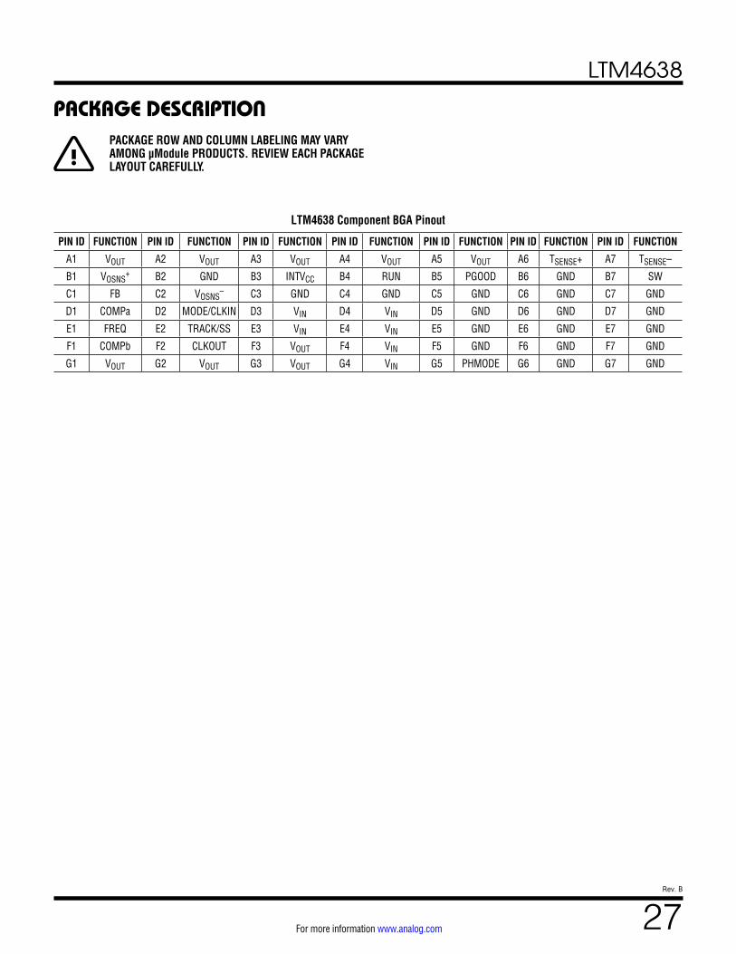
PACKAGE ROW AND COLUMN LABELING MAY VARY AMONG µModule PRODUCTS. REVIEW EACH PACKAGE LAYOUT CAREFULLY.
LTM4638
8Rev. B
For more information www.analog.com
RUN (B4): Run Control Input Pin. Enable regulator opera-tion by tying the specific RUN pin above 1.25V. Tying it below 1.1V shuts down the specific regulator channel.
TSENSE+ (A6): Temperature Monitor Pin. An internal diode
connected PNP transistor is placed between TSENSE+ and
TSENSE– pins. See the Applications Information section.
GND (B2, B6, C3-C7, D5-D7, E5-E7, F5-F7, G6-G7): Power Ground Pins for Both Input and Output Returns. Use large PCB copper areas to connect all GND together.
PIN FUNCTIONSPGOOD (B5): Output Power Good Pin with Open-Drain Logic. PGOOD is pulled to ground when the voltage on the FB pin is not within ±8% of the internal 0.6V reference.
TSENSE– (A7): Low Side of the Internal Temperature Monitor.
SW (B7): Switching node of each channel that is used for testing purposes. Also an R-C snubber network can be applied to reduce or eliminate switch node ringing, or otherwise leave floating. See the Applications Information section.
LTM4638
9Rev. B
For more information www.analog.com
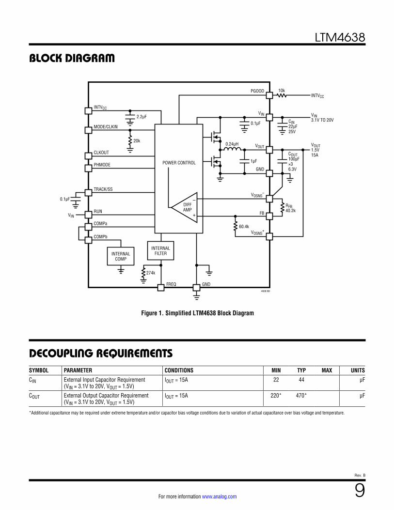
BLOCK DIAGRAM
DECOUPLING REQUIREMENTSSYMBOL PARAMETER CONDITIONS MIN TYP MAX UNITS
CIN External Input Capacitor Requirement (VIN = 3.1V to 20V, VOUT = 1.5V)
IOUT = 15A 22 44 µF
COUT External Output Capacitor Requirement (VIN = 3.1V to 20V, VOUT = 1.5V)
IOUT = 15A 220* 470* µF
*Additional capacitance may be required under extreme temperature and/or capacitor bias voltage conditions due to variation of actual capacitance over bias voltage and temperature.
Figure 1. Simplified LTM4638 Block Diagram
POWER CONTROL
2.2µF
20k
0.1µF
0.1µF CIN22µF25V
INTVCC
TRACK/SS
RUNVIN
MODE/CLKIN
CLKOUT
PHMODE
COMPa
COMPb
1µF
VOUT
VOSNS–
VOSNS+
FB
VIN
10kPGOOD
VOUT1.5V15A
RFB40.2k
60.4k
VIN3.1V TO 20V
INTVCC
GND
0.24µH
4638 BD
FREQ
274k
INTERNALCOMP
GND
INTERNALFILTER
COUT100µF×36.3V
+
–DIFFAMP
LTM4638
10Rev. B
For more information www.analog.com
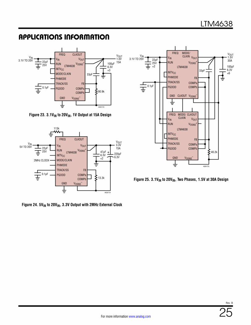
OPERATIONThe LTM4638 is a standalone nonisolated switch mode DC/DC power supply. It can deliver up to 15A DC output current with few external input and output capacitors. This module provides precisely regulated output voltage adjustable between 0.6V to 5.5V via one external resistor over a 3.1V to 20V input voltage range. The typical ap-plication schematic is shown in Figure 23.
The LTM4638 contains an integrated constant on-time valley current mode regulator, power MOSFETs, inductor, and other supporting discrete components. The default switching frequency is 600kHz. For switching noise-sensitive applications, the switching frequency can be adjusted by external resistors and the μModule regulator can be externally synchronized to a clock within ±30% of the set frequency. See the Applications Information section.
With current mode control and internal feedback loop compensation, the LTM4638 module has sufficient stabil-ity margins and good transient performance with a wide range of output capacitors, even with all ceramic output capacitors.
Current mode control provides cycle-by-cycle fast current limiting. Internal output overvoltage and undervoltage comparators pull the open-drain PGOOD output low if the output feedback voltage exits a ±8% window around the regulation point. Continuous operation is forced during OV and UV condition except during start-up when the TRACK pin is ramping up to 0.6V.
Furthermore, in order to protect the internal power MOSFET devices against transient voltage spikes, the LTM4638 constantly monitors the VIN pin for an overvoltage condi-tion. When VIN rises above 24.5V, the regulator suspends operation by shutting off both power MOSFETs. Once VIN drops below 21.5V, the regulator immediately resumes normal operation. The regulator does not execute its soft-start function when exiting an overvoltage condition.
Multiphase operation can be easily employed with the synchronization and phase mode controls. Up to 6 phases can be cascaded to run simultaneously with respect to each other by programming the PHMODE pin to different levels. The LTM4638 has MODE/CLKIN and CLKOUT pins for PolyPhase operation of multiple devices or frequency synchronization.
Pulling the RUN pin to GND forces the controller into its shutdown state, turning off both power MOSFETs and most of the internal control circuitry. At light load currents, discontinuous mode (DCM) operation can be enabled to achieve higher efficiency compared to continuous mode (CCM) by pulling the MODE/CLKIN pin to GND. The TRACK/SS pin is used for power supply tracking and soft-start programming. See the Applications Informa-tion section.
LTM4638
11Rev. B
For more information www.analog.com
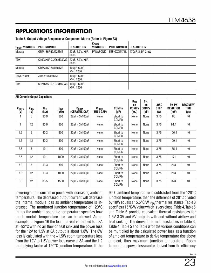
APPLICATIONS INFORMATIONThe typical LTM4638 application circuit is shown in Figure 23. External component selection is primarily determined by the input voltage, the output voltage and the maximum load current. Refer to Table 7 for specific external capacitor requirements for a particular application.
VIN to VOUT Step-Down Ratios
There are restrictions in the maximum VIN and VOUT step-down ratios that can be achieved for a given input voltage due to the minimum off-time and minimum on-time limits of the regulator. The minimum off-time limit imposes a maximum duty cycle which can be calculated as:
DMAX = 1 – (tOFF(MIN) • fSW)
where tOFF(MIN) is the minimum off-time, typically 50ns for LTM4638, and fSW (Hz) is the switching frequency. Conversely the minimum on-time limit imposes a minimum duty cycle of the converter which can be calculated as:
DMIN = tON(MIN) • fSW
where tON(MIN) is the minimum on-time, typically 25ns for LTM4638. In the rare cases where the minimum duty cycle is surpassed, the output voltage will still remain in regulation, but the switching frequency will decrease from its programmed value. Note that additional thermal derating may be applied. See the Thermal Considerations and Output Current Derating section in this data sheet.
Output Voltage Programming
The PWM controller has an internal 0.6V reference voltage. As shown in the Block Diagram, a 60.4k internal feedback resistor connects the VOUT and FB pins together. Adding a resistor, RFB, from FB pin to VOSNS
– programs the output voltage:
RFB =
0.6VVOUT – 0.6V
• 60.4k
Table 1. RFB Resistor Table vs Various Output VoltagesVOUT (V) 0.6 1.0 1.2 1.5 1.8 2.5 3.3 5.0
RFB (kΩ) OPEN 90.9 60.4 40.2 30.1 19.1 13.3 8.25
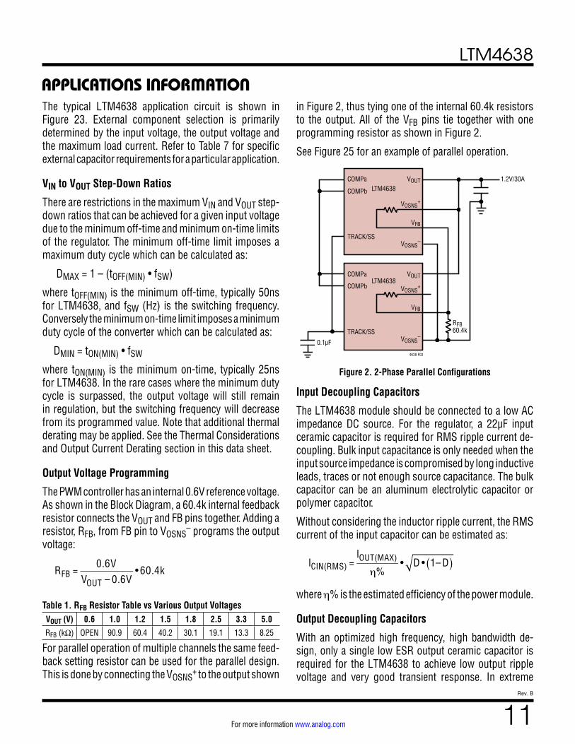
For parallel operation of multiple channels the same feed-back setting resistor can be used for the parallel design. This is done by connecting the VOSNS
+ to the output shown
in Figure 2, thus tying one of the internal 60.4k resistors to the output. All of the VFB pins tie together with one programming resistor as shown in Figure 2.
See Figure 25 for an example of parallel operation.
Input Decoupling Capacitors
The LTM4638 module should be connected to a low AC impedance DC source. For the regulator, a 22µF input ceramic capacitor is required for RMS ripple current de-coupling. Bulk input capacitance is only needed when the input source impedance is compromised by long inductive leads, traces or not enough source capacitance. The bulk capacitor can be an aluminum electrolytic capacitor or polymer capacitor.
Without considering the inductor ripple current, the RMS current of the input capacitor can be estimated as:
ICIN(RMS) =
IOUT(MAX)
η%• D • 1– D( )
where η% is the estimated efficiency of the power module.
Output Decoupling Capacitors
With an optimized high frequency, high bandwidth de-sign, only a single low ESR output ceramic capacitor is required for the LTM4638 to achieve low output ripple voltage and very good transient response. In extreme
4638 F02
COMPa
COMPb
1.2V/30AVOUT
VOSNS+
VOSNS–
VFB
LTM4638
TRACK/SS
COMPa VOUT
VOSNS+
VOSNS–
VFB
LTM4638
TRACK/SS
0.1µF
RFB60.4k
COMPb
Figure 2. 2-Phase Parallel Configurations
LTM4638
12Rev. B
For more information www.analog.com
APPLICATIONS INFORMATIONcold or hot temperature or high output voltage case, ad-ditional ceramic capacitor or tantalum-polymer capacitor is required due to variation of actual capacitance over bias voltage and temperature. Table 7 shows a matrix of dif-ferent output voltages and output capacitors to minimize the voltage droop and overshoot during a 4A load-step transient. Additional output filtering may be required by the system designer if further reduction of output ripple or dynamic transient spikes is required. The Linear Technology LTpowerCAD™ design tool is available to download online for output ripple, stability and transient response analysis for further optimization.
Discontinuous Current Mode (DCM)
In applications where low output ripple and high efficiency at intermediate current are desired, discontinuous current mode (DCM) should be used by connecting the MODE/CLKIN pin to GND. At light loads the internal current com-parator may remain tripped for several cycles and force the top MOSFET to stay off for several cycles, thus skipping cycles. The inductor current does not reverse in this mode.
Forced Continuous Current Mode (CCM)
In applications where fixed frequency operation is more critical than low current efficiency, and where the lowest output ripple is desired, forced continuous operation should be used. Forced continuous operation can be enabled by tying the MODE/CLKIN pin to INTVCC. In this mode, induc-tor current is allowed to reverse during low output loads, the COMP voltage is in control of the current comparator threshold throughout, and the top MOSFET always turns on with each oscillator pulse. During start-up, forced continuous mode is disabled and inductor current is prevented from reversing until the LTM4638’s output voltage is in regulation.
Operating Frequency
The operating frequency of the LTM4638 is optimized to achieve the compact package size and the minimum out-put ripple voltage while still keeping high efficiency. The default operating frequency is 600kHz. In most ap-plications, no additional frequency adjustment is required.
If an operating frequency other than 600kHz is required by the application, the operating frequency can be increased
by adding a resistor, RFSET, between the FREQ pin and SGND, as shown in Figure 24. The operating frequency can be calculated as:
f Hz( ) =
1.67e11274k ||RFSET Ω( )
The programmable operating frequency range is from 400kHz to 3MHz.
Frequency Synchronization and Clock In
The power module has a phase-locked loop comprised of an internal voltage controlled oscillator and a phase detector. This allows the internal top MOSFET turn-on to be locked to the rising edge of the external clock. The external clock frequency range must be within ±30% around the resistor set operating frequency. A pulse detection circuit is used to detect a clock on the CLKIN pin to turn on the phase-locked loop. The pulse width of the clock has to be at least 100ns. The clock high level must be above 1V and clock low level below 0.3V. During the start-up of the regulator, the phase-locked loop function is disabled.
Multiphase Operation
For output loads that demand more than 15A of current, multiple LTM4638s can be paralleled to run out of phase to provide more output current without increasing input and output voltage ripples.
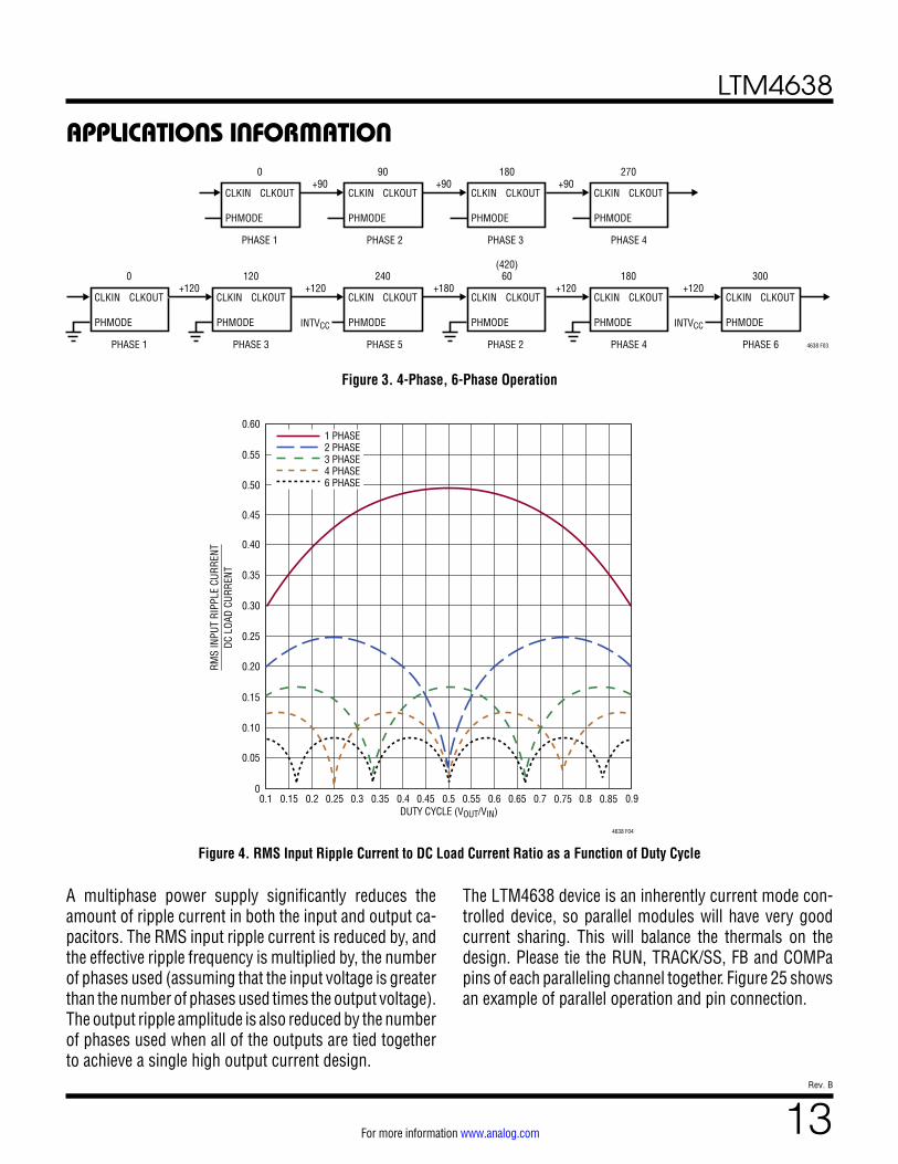
The CLKOUT signal can be connected to the MODE/CLKIN pin of the following LTM4638 stage to line up both the frequency and the phase of the entire system. Tying the PHMODE pin to INTVCC, GND or FLOAT generates a phase difference (between CLKIN and CLKOUT) of 180°, 120°, or 90° respectively, which corresponds to 2-phase, 3-phase or 4-phase operation. A total of 6 phases can be cascaded to run simultaneously out of phase with respect to each other by programming the PHMODE pin of each LTM4638 to different levels. Figure 3 shows a 4-phase design and a 6-phase design example for clock phasing.
Table 2. PHMODE Pin Status and Corresponding PhaseRelationship (Relative to CLKIN)
PHMODE INTVCC GND FLOAT
CLKOUT 180° 120° 90°
LTM4638
13Rev. B
For more information www.analog.com
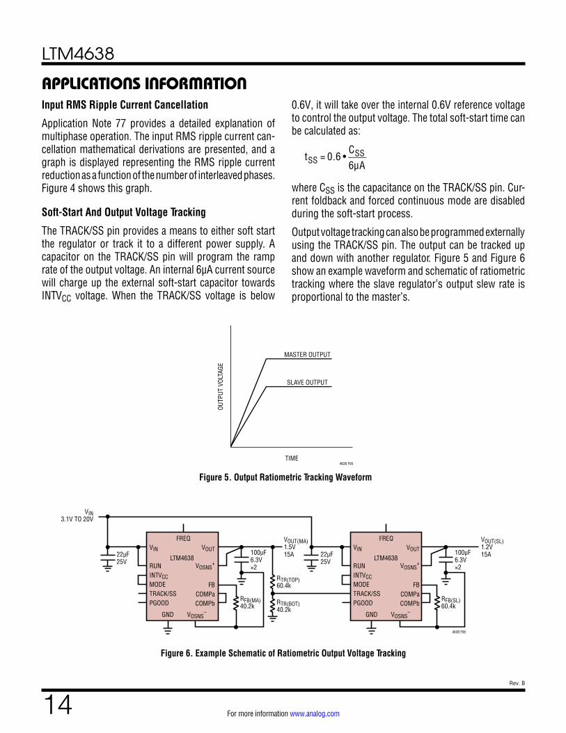
A multiphase power supply significantly reduces the amount of ripple current in both the input and output ca-pacitors. The RMS input ripple current is reduced by, and the effective ripple frequency is multiplied by, the number of phases used (assuming that the input voltage is greater than the number of phases used times the output voltage). The output ripple amplitude is also reduced by the number of phases used when all of the outputs are tied together to achieve a single high output current design.
The LTM4638 device is an inherently current mode con-trolled device, so parallel modules will have very good current sharing. This will balance the thermals on the design. Please tie the RUN, TRACK/SS, FB and COMPa pins of each paralleling channel together. Figure 25 shows an example of parallel operation and pin connection.
APPLICATIONS INFORMATION
Figure 3. 4-Phase, 6-Phase Operation
Figure 4. RMS Input Ripple Current to DC Load Current Ratio as a Function of Duty Cycle
4638 F03
CLKIN
PHMODE
CLKOUT
0 90 180 270+90 +90 +90
PHASE 4PHASE 3PHASE 2PHASE 1
CLKIN
PHMODE
CLKOUT CLKIN
PHMODE
CLKOUT CLKIN
PHMODE
CLKOUT
CLKIN
PHMODE
CLKOUT
120 240(420)
60 180+120 +180 +120
PHASE 4
INTVCCINTVCC
PHASE 2PHASE 5PHASE 3
CLKIN
PHMODE
CLKOUT CLKIN
PHMODE
CLKOUT CLKIN
PHMODE
CLKOUT
300+120
PHASE 6
CLKIN
PHMODE
CLKOUT
0
PHASE 1
CLKIN
PHMODE
CLKOUT+120
0.75 0.8
4638 F04
0.70.650.60.550.50.450.40.350.30.250.20.150.1 0.85 0.9DUTY CYCLE (VOUT/VIN)
0
DC L
OAD
CURR
ENT
RMS
INPU
T RI
PPLE
CUR
RENT
0.05
0.10
0.15
0.20
0.25
0.30
0.35
0.40
0.45
0.50
0.55
0.601 PHASE2 PHASE3 PHASE4 PHASE6 PHASE
LTM4638
14Rev. B
For more information www.analog.com
APPLICATIONS INFORMATIONInput RMS Ripple Current Cancellation
Application Note 77 provides a detailed explanation of multiphase operation. The input RMS ripple current can-cellation mathematical derivations are presented, and a graph is displayed representing the RMS ripple current reduction as a function of the number of interleaved phases. Figure 4 shows this graph.
Soft-Start And Output Voltage Tracking
The TRACK/SS pin provides a means to either soft start the regulator or track it to a different power supply. A capacitor on the TRACK/SS pin will program the ramp rate of the output voltage. An internal 6µA current source will charge up the external soft-start capacitor towards INTVCC voltage. When the TRACK/SS voltage is below
0.6V, it will take over the internal 0.6V reference voltage to control the output voltage. The total soft-start time can be calculated as:
tSS = 0.6 •
CSS6µA
where CSS is the capacitance on the TRACK/SS pin. Cur-rent foldback and forced continuous mode are disabled during the soft-start process.
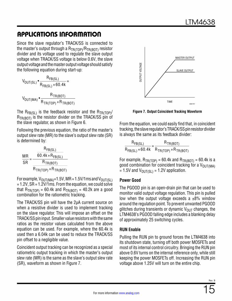
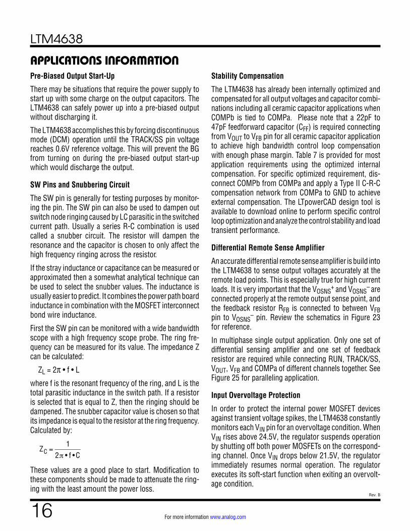
Output voltage tracking can also be programmed externally using the TRACK/SS pin. The output can be tracked up and down with another regulator. Figure 5 and Figure 6 show an example waveform and schematic of ratiometric tracking where the slave regulator’s output slew rate is proportional to the master’s.
Figure 5. Output Ratiometric Tracking Waveform
Figure 6. Example Schematic of Ratiometric Output Voltage Tracking
TIME
SLAVE OUTPUT
MASTER OUTPUT
OUTP
UT V
OLTA
GE
4638 F05
FREQVIN
RUNINTVCCMODETRACK/SSPGOOD
VOUT
VOSNS+
FBCOMPaCOMPb
GND VOSNS–
RFB(MA)40.2k
LTM463822µF25V
VIN3.1V TO 20V
VOUT(MA)1.5V15A100µF
6.3V×2
RTR(BOT)40.2k
RFB(SL)60.4k
RTR(TOP)60.4k
FREQVIN
RUNINTVCCMODETRACK/SSPGOOD
VOUT
FBCOMPaCOMPb
GND VOSNS–
4638 F06
LTM463822µF25V
VOUT(SL)1.2V15A100µF
6.3V×2VOSNS
+
LTM4638
15Rev. B
For more information www.analog.com
APPLICATIONS INFORMATIONSince the slave regulator’s TRACK/SS is connected to the master’s output through a RTR(TOP)/RTR(BOT) resistor divider and its voltage used to regulate the slave output voltage when TRACK/SS voltage is below 0.6V, the slave output voltage and the master output voltage should satisfy the following equation during start-up:
VOUT(SL) •RFB(SL)
RFB(SL) + 60.4k=
VOUT(MA) •RTR(BOT)
RTR(TOP) +RTR(BOT)
The RFB(SL) is the feedback resistor and the RTR(TOP)/RTR(BOT) is the resistor divider on the TRACK/SS pin of the slave regulator, as shown in Figure 6.
Following the previous equation, the ratio of the master’s output slew rate (MR) to the slave’s output slew rate (SR) is determined by:
MRSR
=
RFB(SL)
60.4k +RFB(SL)RTR(BOT)
RTR(TOP) +RTR(BOT)
For example, VOUT(MA)=1.5V, MR = 1.5V/1ms and VOUT(SL) = 1.2V, SR = 1.2V/1ms. From the equation, we could solve that RTR(TOP) = 60.4k and RTR(BOT) = 40.2k are a good combination for the ratiometric tracking.
The TRACK/SS pin will have the 2µA current source on when a resistive divider is used to implement tracking on the slave regulator. This will impose an offset on the TRACK/SS pin input. Smaller value resistors with the same ratios as the resistor values calculated from the above equation can be used. For example, where the 60.4k is used then a 6.04k can be used to reduce the TRACK/SS pin offset to a negligible value.
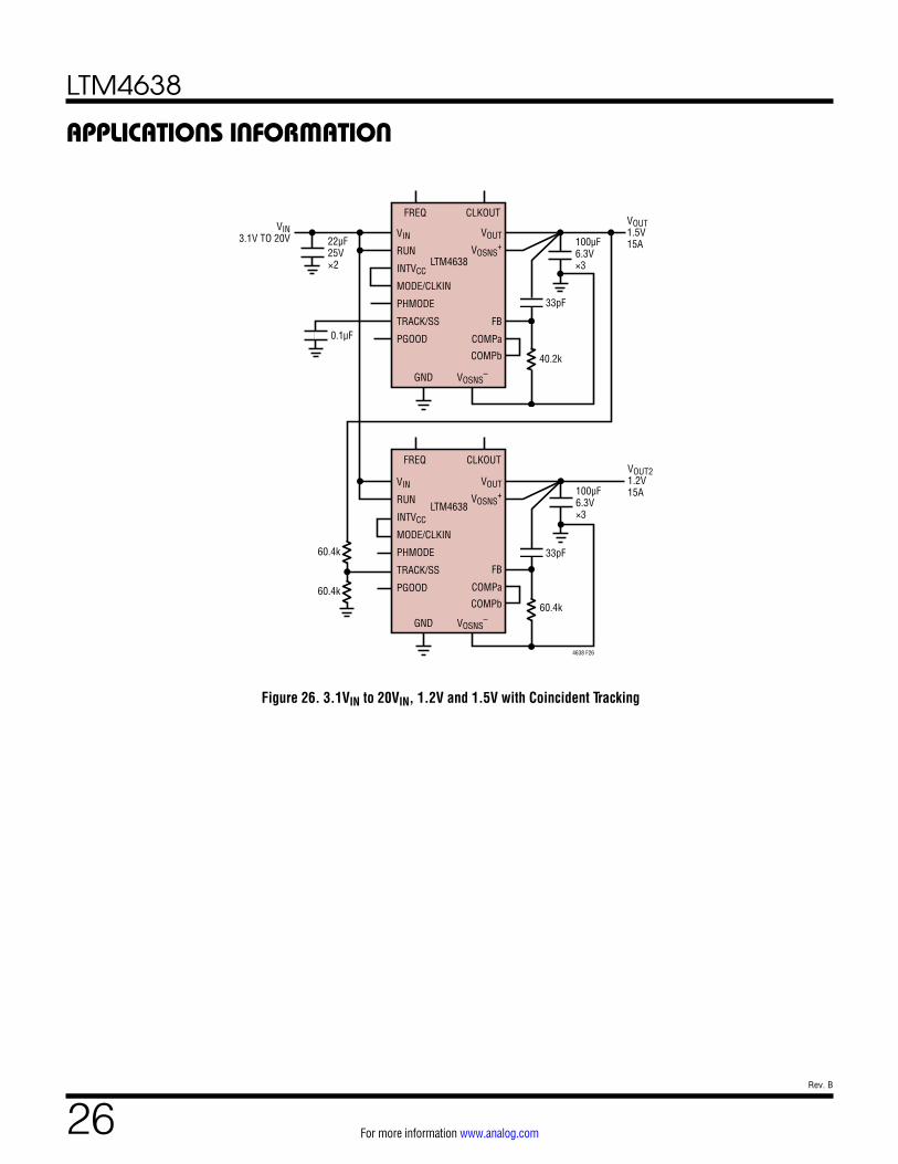
Coincident output tracking can be recognized as a special ratiometric output tracking in which the master’s output slew rate (MR) is the same as the slave’s output slew rate (SR), waveform as shown in Figure 7.
Figure 7. Output Coincident Tracking Waveform
From the equation, we could easily find that, in coincident tracking, the slave regulator’s TRACK/SS pin resistor divider is always the same as its feedback divider:
RFB(SL)
RFB(SL) + 60.4k=
RTR(BOT)
RTR(TOP) +RTR(BOT)
For example, RTR(TOP) = 60.4k and RTR(BOT) = 60.4k is a good combination for coincident tracking for a VOUT(MA) = 1.5V and VOUT(SL) = 1.2V application.
Power Good
The PGOOD pin is an open-drain pin that can be used to monitor valid output voltage regulation. This pin is pulled low when the output voltage exceeds a ±8% window around the regulation point. To prevent unwanted PGOOD glitches during transients or dynamic VOUT changes, the LTM4638’s PGOOD falling edge includes a blanking delay of approximately 25 switching cycles.
RUN Enable
Pulling the RUN pin to ground forces the LTM4638 into its shutdown state, turning off both power MOSFETs and most of its internal control circuitry. Bringing the RUN pin above 0.6V turns on the internal reference only, while still keeping the power MOSFETs off. Increasing the RUN pin voltage above 1.25V will turn on the entire chip.
TIME
MASTER OUTPUT
SLAVE OUTPUT
OUTP
UT V
OLTA
GE
4638 F07
LTM4638
16Rev. B
For more information www.analog.com
APPLICATIONS INFORMATIONPre-Biased Output Start-Up
There may be situations that require the power supply to start up with some charge on the output capacitors. The LTM4638 can safely power up into a pre-biased output without discharging it.
The LTM4638 accomplishes this by forcing discontinuous mode (DCM) operation until the TRACK/SS pin voltage reaches 0.6V reference voltage. This will prevent the BG from turning on during the pre-biased output start-up which would discharge the output.
SW Pins and Snubbering Circuit
The SW pin is generally for testing purposes by monitor-ing the pin. The SW pin can also be used to dampen out switch node ringing caused by LC parasitic in the switched current path. Usually a series R-C combination is used called a snubber circuit. The resistor will dampen the resonance and the capacitor is chosen to only affect the high frequency ringing across the resistor.
If the stray inductance or capacitance can be measured or approximated then a somewhat analytical technique can be used to select the snubber values. The inductance is usually easier to predict. It combines the power path board inductance in combination with the MOSFET interconnect bond wire inductance.
First the SW pin can be monitored with a wide bandwidth scope with a high frequency scope probe. The ring fre-quency can be measured for its value. The impedance Z can be calculated:
ZL = 2π • f • L
where f is the resonant frequency of the ring, and L is the total parasitic inductance in the switch path. If a resistor is selected that is equal to Z, then the ringing should be dampened. The snubber capacitor value is chosen so that its impedance is equal to the resistor at the ring frequency. Calculated by:
ZC =
12π • f •C
These values are a good place to start. Modification to these components should be made to attenuate the ring-ing with the least amount the power loss.
Stability Compensation
The LTM4638 has already been internally optimized and compensated for all output voltages and capacitor combi-nations including all ceramic capacitor applications when COMPb is tied to COMPa. Please note that a 22pF to 47pF feedforward capacitor (CFF) is required connecting from VOUT to VFB pin for all ceramic capacitor application to achieve high bandwidth control loop compensation with enough phase margin. Table 7 is provided for most application requirements using the optimized internal compensation. For specific optimized requirement, dis-connect COMPb from COMPa and apply a Type II C-R-C compensation network from COMPa to GND to achieve external compensation. The LTpowerCAD design tool is available to download online to perform specific control loop optimization and analyze the control stability and load transient performance.
Differential Remote Sense Amplifier
An accurate differential remote sense amplifier is build into the LTM4638 to sense output voltages accurately at the remote load points. This is especially true for high current loads. It is very important that the VOSNS
+ and VOSNS– are
connected properly at the remote output sense point, and the feedback resistor RFB is connected to between VFB pin to VOSNS
– pin. Review the schematics in Figure 23 for reference.
In multiphase single output application. Only one set of differential sensing amplifier and one set of feedback resistor are required while connecting RUN, TRACK/SS, VOUT, VFB and COMPa of different channels together. See Figure 25 for paralleling application.
Input Overvoltage Protection
In order to protect the internal power MOSFET devices against transient voltage spikes, the LTM4638 constantly monitors each VIN pin for an overvoltage condition. When VIN rises above 24.5V, the regulator suspends operation by shutting off both power MOSFETs on the correspond-ing channel. Once VIN drops below 21.5V, the regulator immediately resumes normal operation. The regulator executes its soft-start function when exiting an overvolt-age condition.
LTM4638
17Rev. B
For more information www.analog.com
APPLICATIONS INFORMATIONTemperature Monitoring
Measuring the absolute temperature of a diode is possible due to the relationship between current, voltage and tem-perature described by the classic diode equation:
ID = IS • eVD
η • VT
⎛
⎝⎜⎞
⎠⎟
or
VD = η • VT •InIDIS
where ID is the diode current, VD is the diode voltage, η is the ideality factor (typically close to 1.0) and IS (satura-tion current) is a process dependent parameter. VT can be broken out to:
VT =
k • Tq
where T is the diode junction temperature in Kelvin, q is the electron charge and k is Boltzmann’s constant. VT is approximately 26mV at room temperature (298K) and scales linearly with Kelvin temperature. It is this linear temperature relationship that makes diodes suitable tem-perature sensors. The IS term in the previous equation is the extrapolated current through a diode junction when the diode has zero volts across the terminals. The IS term varies from process to process, varies with temperature, and by definition must always be less than ID. Combining all of the constants into one term:
KD =
η • kq
where KD = 8.62−5, and knowing ln(ID/IS) is always posi-tive because ID is always greater than IS, leaves us with the equation that:
VD = T KELVIN( ) •KD •In
IDIS
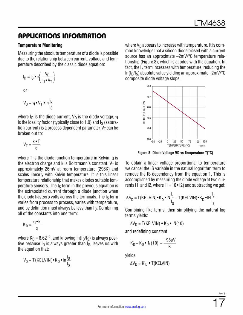
where VD appears to increase with temperature. It is com-mon knowledge that a silicon diode biased with a current source has an approximate –2mV/°C temperature rela-tionship (Figure 8), which is at odds with the equation. In fact, the IS term increases with temperature, reducing the ln(ID/IS) absolute value yielding an approximate –2mV/°C composite diode voltage slope.
TEMPERATURE (°C)–50 –25
0.3
DIOD
E VO
LTAG
E (V
)
0.5
0.8
0 50 75
0.4
0.7
0.6
25 1004638 F08
125
Figure 8. Diode Voltage VD vs Temperature T(°C)
To obtain a linear voltage proportional to temperature we cancel the IS variable in the natural logarithm term to remove the IS dependency from the equation 1. This is accomplished by measuring the diode voltage at two cur-rents I1, and I2, where I1 = 10 • I2) and subtracting we get:
ΔVD = T(KELVIN)•KD •IN
I1IS
− T(KELVIN)•KD •INI2IS
Combining like terms, then simplifying the natural log terms yields:
ΔVD = T(KELVIN) • KD • lN(10)
and redefining constant
K'D = KD •IN(10) =
198µVK
yields
ΔVD = K’D • T(KELVIN)
LTM4638
18Rev. B
For more information www.analog.com
Solving for temperature:
T(KELVIN) =
ΔVDK'D
(°CELSIUS) = T(KELVIN)– 273.15
where
300°K = 27°C
means that is we take the difference in voltage across the diode measured at two currents with a ratio of 10, the resulting voltage is 198μV per Kelvin of the junction with a zero intercept at 0 Kelvin.
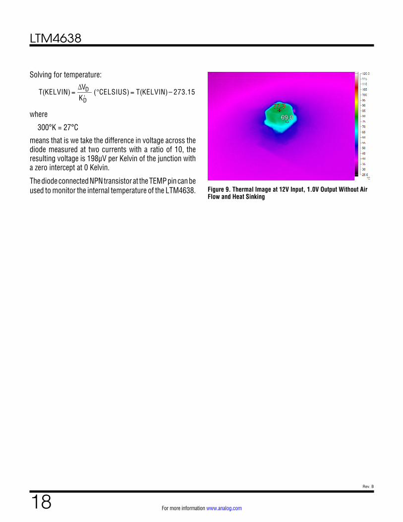
The diode connected NPN transistor at the TEMP pin can be used to monitor the internal temperature of the LTM4638. Figure 9. Thermal Image at 12V Input, 1.0V Output Without Air
Flow and Heat Sinking
LTM4638
19Rev. B
For more information www.analog.com
APPLICATIONS INFORMATIONThermal Considerations and Output Current Derating
The thermal resistances reported in the Pin Configuration section of the data sheet are consistent with those param-eters defined by JESD 51-12 and are intended for use with finite element analysis (FEA) software modeling tools that leverage the outcome of thermal modeling, simulation, and correlation to hardware evaluation performed on a µModule package mounted to a hardware test board. The motivation for providing these thermal coefficients is found in JESD 51-12 (Guidelines for Reporting and Using Electronic Package Thermal Information).
Many designers may opt to use laboratory equipment and a test vehicle such as the demo board to anticipate the µModule regulator’s thermal performance in their ap-plication at various electrical and environmental operating conditions to compliment any FEA activities. Without FEA software, the thermal resistances reported in the Pin Con-figuration section are, in and of themselves, not relevant to providing guidance of thermal performance; instead, the derating curves provided in this data sheet can be used in a manner that yields insight and guidance pertaining to one’s application usage, and can be adapted to correlate thermal performance to one’s own application.
The Pin Configuration section gives four thermal coeffi-cients explicitly defined in JESD 51-12; these coefficients are quoted or paraphrased below:
1. θJA, the thermal resistance from junction to ambient, is the natural convection junction-to-ambient air thermal resistance measured in a one cubic foot sealed enclo-sure. This environment is sometimes referred to as “still air” although natural convection causes the air to move. This value is determined with the part mounted to a 95mm × 76mm PCB with four layers.
2. θJCbottom, the thermal resistance from junction to the bottom of the product case, is determined with all of the component power dissipation flowing through the bottom of the package. In the typical µModule regulator, the bulk of the heat flows out the bottom of the pack-age, but there is always heat flow out into the ambient environment. As a result, this thermal resistance value may be useful for comparing packages, but the test conditions don’t generally match the user’s application.
3. θJCtop, the thermal resistance from junction to top of the product case, is determined with nearly all of the component power dissipation flowing through the top of the package. As the electrical connections of the typical µModule regulator are on the bottom of the package, it is rare for an application to operate such that most of the heat flows from the junction to the top of the part. As in the case of θJCbottom, this value may be useful for comparing packages but the test conditions don’t generally match the user’s application.
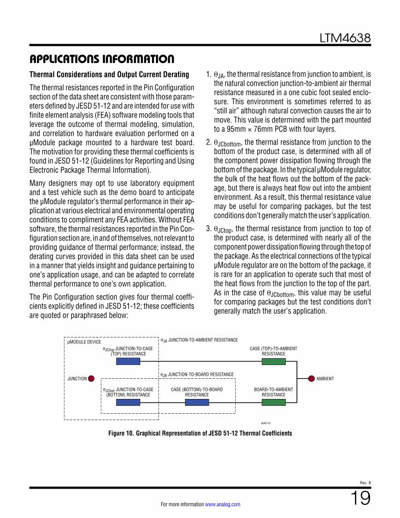
Figure 10. Graphical Representation of JESD 51-12 Thermal Coefficients
4638 F10
µMODULE DEVICEθJCtop JUNCTION-TO-CASE
(TOP) RESISTANCE
θJB JUNCTION-TO-BOARD RESISTANCE
θJA JUNCTION-TO-AMBIENT RESISTANCE
CASE (TOP)-TO-AMBIENTRESISTANCE
BOARD-TO-AMBIENTRESISTANCE
θJCbot JUNCTION-TO-CASE(BOTTOM) RESISTANCE
JUNCTION AMBIENT
CASE (BOTTOM)-TO-BOARDRESISTANCE
LTM4638
20Rev. B
For more information www.analog.com
APPLICATIONS INFORMATION4. θJB, the thermal resistance from junction to the printed
circuit board, is the junction-to-board thermal resistance where almost all of the heat flows through the bottom of the µModule package and into the board, and is really the sum of the θJCbottom and the thermal resistance of the bottom of the part through the solder joints and through a portion of the board. The board temperature is measured a specified distance from the package.
A graphical representation of the aforementioned thermal resistances is given in Figure 10; blue resistances are contained within the μModule regulator, whereas green resistances are external to the µModule package.
As a practical matter, it should be clear to the reader that no individual or sub-group of the four thermal resistance parameters defined by JESD 51-12 or provided in the Pin Configuration section replicates or conveys normal operating conditions of a μModule regulator. For example, in normal board-mounted applications, never does 100% of the device’s total power loss (heat) thermally conduct exclusively through the top or exclusively through bot-tom of the µModule package—as the standard defines for θJCtop and θJCbottom, respectively. In practice, power loss is thermally dissipated in both directions away from the package—granted, in the absence of a heat sink and airflow, a majority of the heat flow is into the board.
Within the LTM4638 be aware there are multiple power devices and components dissipating power, with a con-sequence that the thermal resistances relative to different junctions of components or die are not exactly linear with respect to total package power loss. To reconcile this complication without sacrificing modeling simplicity—but also, not ignoring practical realities—an approach has been taken using FEA software modeling along with laboratory testing in a controlled environment chamber to reason-ably define and correlate the thermal resistance values supplied in this data sheet: (1) Initially, FEA software is used to accurately build the mechanical geometry of the LTM4638 and the specified PCB with all of the correct material coefficients along with accurate power loss source definitions; (2) this model simulates a software-defined JEDEC environment consistent with JSED 51-12 to predict power loss heat flow and temperature readings at different interfaces that enable the calculation of the JEDEC-defined
thermal resistance values; (3) the model and FEA software is used to evaluate the LTM4638 with heat sink and airflow; (4) having solved for and analyzed these thermal resistance values and simulated various operating conditions in the software model, a thorough laboratory evaluation replicates the simulated conditions with thermocouples within a controlled environment chamber while operating the device at the same power loss as that which was simulated. An outcome of this process and due diligence yields the set of derating curves shown in this data sheet. After these laboratory tests have been performed and correlated to the LTM4638 model, then the θJB and θBA are summed together to provide a value that should closely equal the θJA value because approximately 100% of power loss flows from the junction through the board into ambient with no airflow or top mounted heat sink.
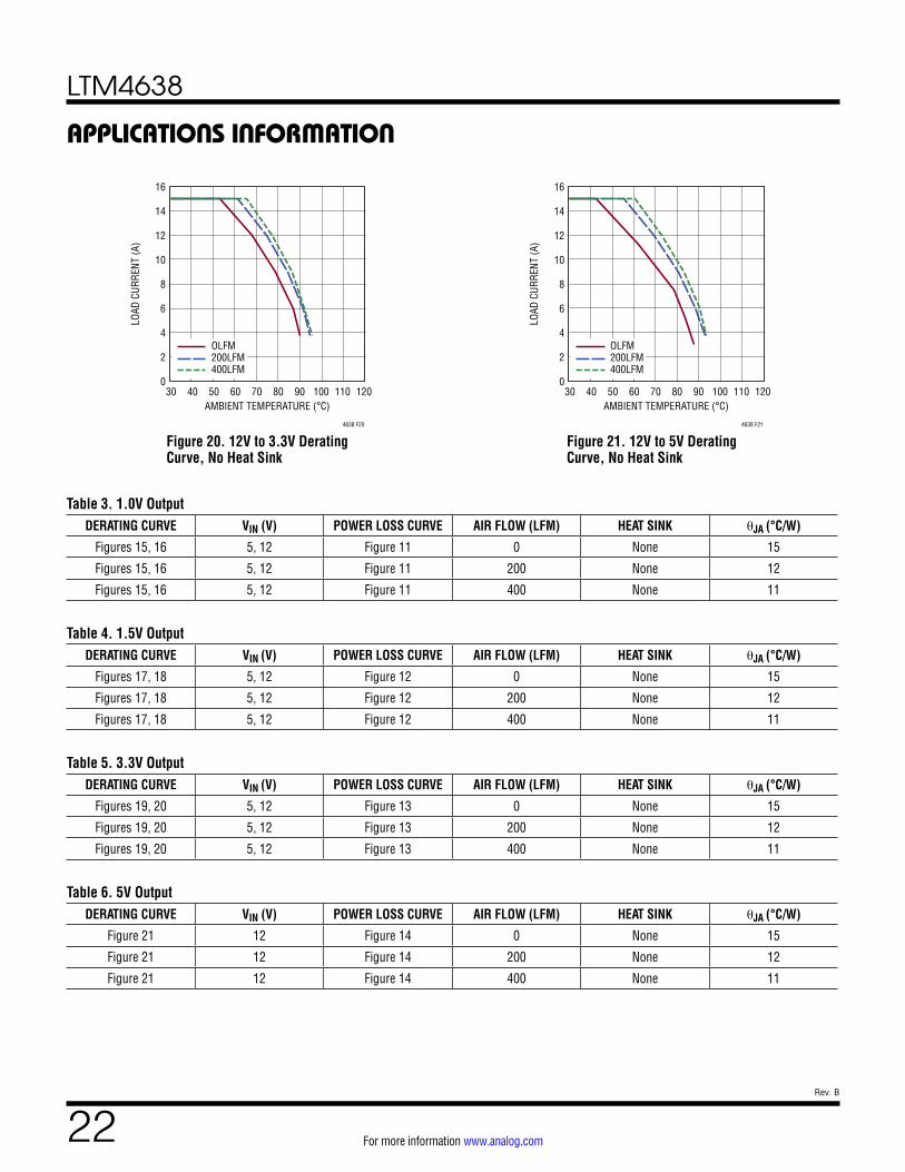
The 1.0V, 1.5V, 3.3V and 5V power loss curves in Figure 11 to Figure 14 can be used in coordination with the load current derating curves in Figure 15 to Figure 21 for calculating an approximate θJA thermal resistance for the LTM4638 with various airflow conditions. The power loss curves are taken at room temperature, and are increased with a multiplicative factor according to the ambient temperature. This approximate factor is: 1.2 for 120°C at junction temperature. Maximum load current is achievable while increasing ambient temperature as long as the junction temperature is less than 120°C, which is a 5°C guard band from maximum junction temperature of 125°C. When the ambient temperature reaches a point where the junction temperature is 120°C, then the load current is lowered to maintain the junction at 120°C while increasing ambient temperature up to 120°C. The derat-ing curves are plotted with the output current starting at 15A and the ambient temperature at 30°C. The output voltages are 1.0V, 1.5V, 3.3V and 5V. These are chosen to include the lower and higher output voltage ranges for correlating the thermal resistance. Thermal models are derived from several temperature measurements in a controlled temperature chamber along with thermal modeling analysis. The junction temperatures are moni-tored while ambient temperature is increased with and without airflow. The power loss increase with ambient temperature change is factored into the derating curves. The junctions are maintained at 120°C maximum while
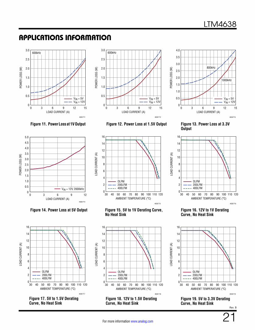
LTM4638
21Rev. B
For more information www.analog.com
Figure 19. 5V to 3.3V Derating Curve, No Heat Sink
Figure 11. Power Loss at 1V Output Figure 12. Power Loss at 1.5V Output Figure 13. Power Loss at 3.3V Output
APPLICATIONS INFORMATION
Figure 17. 5V to 1.5V Derating Curve, No Heat Sink
Figure 15. 5V to 1V Derating Curve, No Heat Sink
Figure 16. 12V to 1V Derating Curve, No Heat Sink
Figure 18. 12V to 1.5V Derating Curve, No Heat Sink
LOAD CURRENT (A)0
0
POW
ER L
OSS
(W) 2.0
2.5
1.5
0.5
1.0
3.0
9 12 153 6
4638 F11
600kHz
VIN = 12VVIN = 5V
LOAD CURRENT (A)0
0
POW
ER L
OSS
(W)
3.0
2.5
1.5
1.0
0.5
2.0
9 12 153 6
4638 F12
600kHz
VIN = 12VVIN = 5V
LOAD CURRENT (A)0
0
POW
ER L
OSS
(W)
3.0
3.5
2.5
1.5
1.0
0.5
2.0
4.0
9 12 153 6
4638 F13
800kHz
1000kHz
VIN = 12VVIN = 5V
AMBIENT TEMPERATURE (°C)30
0
LOAD
CUR
RENT
(A)
12
14
10
6
4
2
8
16
908070 110100 12040 6050
4638 F15
400LFM200LFMOLFM
AMBIENT TEMPERATURE (°C)30
0
LOAD
CUR
RENT
(A)
12
14
10
6
4
2
8
16
908070 110100 12040 6050
4638 F16
400LFM200LFMOLFM
AMBIENT TEMPERATURE (°C)30
0
LOAD
CUR
RENT
(A)
12
14
10
6
4
2
8
16
908070 110100 12040 6050
4638 F17
400LFM200LFMOLFM
AMBIENT TEMPERATURE (°C)30
0
LOAD
CUR
RENT
(A)
12
14
10
6
4
2
8
16
908070 110100 12040 6050
4638 F18
400LFM200LFMOLFM
AMBIENT TEMPERATURE (°C)30
0
LOAD
CUR
RENT
(A)
12
14
10
6
4
2
8
16
908070 110100 12040 6050
4638 F19
400LFM200LFMOLFM
LOAD CURRENT (A)0
POW
ER L
OSS
(W)
3.0
5.0
4.5
4.0
3.5
2.5
1.5
0.5
2.0
1.0
096
4638 F14
123
VIN = 12V, 2000kHz
Figure 14. Power Loss at 5V Output
LTM4638
22Rev. B
For more information www.analog.com
APPLICATIONS INFORMATION
Figure 20. 12V to 3.3V Derating Curve, No Heat Sink
Figure 21. 12V to 5V Derating Curve, No Heat Sink
Table 3. 1.0V OutputDERATING CURVE VIN (V) POWER LOSS CURVE AIR FLOW (LFM) HEAT SINK θJA (°C/W)
Figures 15, 16 5, 12 Figure 11 0 None 15
Figures 15, 16 5, 12 Figure 11 200 None 12
Figures 15, 16 5, 12 Figure 11 400 None 11
Table 4. 1.5V OutputDERATING CURVE VIN (V) POWER LOSS CURVE AIR FLOW (LFM) HEAT SINK θJA (°C/W)
Figures 17, 18 5, 12 Figure 12 0 None 15
Figures 17, 18 5, 12 Figure 12 200 None 12
Figures 17, 18 5, 12 Figure 12 400 None 11
Table 5. 3.3V OutputDERATING CURVE VIN (V) POWER LOSS CURVE AIR FLOW (LFM) HEAT SINK θJA (°C/W)
Figures 19, 20 5, 12 Figure 13 0 None 15
Figures 19, 20 5, 12 Figure 13 200 None 12
Figures 19, 20 5, 12 Figure 13 400 None 11
Table 6. 5V OutputDERATING CURVE VIN (V) POWER LOSS CURVE AIR FLOW (LFM) HEAT SINK θJA (°C/W)
Figure 21 12 Figure 14 0 None 15
Figure 21 12 Figure 14 200 None 12
Figure 21 12 Figure 14 400 None 11
AMBIENT TEMPERATURE (°C)30
0
LOAD
CUR
RENT
(A)
12
14
10
6
4
2
8
16
908070 110100 12040 6050
4638 F20
400LFM200LFMOLFM
AMBIENT TEMPERATURE (°C)30
0
LOAD
CUR
RENT
(A)
12
14
10
6
4
2
8
16
908070 110100 12040 6050
4638 F21
400LFM200LFMOLFM
LTM4638
23Rev. B
For more information www.analog.com
lowering output current or power with increasing ambient temperature. The decreased output current will decrease the internal module loss as ambient temperature is in-creased. The monitored junction temperature of 120°C minus the ambient operating temperature specifies how much module temperature rise can be allowed. As an example, in Figure 16 the load current is derated to ~8A at ~92°C with no air flow or heat sink and the power loss for the 12V to 1.5V at 8A output is about 1.8W. The 8W loss is calculated with the ~1.5W room temperature loss from the 12V to 1.5V power loss curve at 8A, and the 1.2 multiplying factor at 120°C junction temperature. If the
APPLICATIONS INFORMATIONTable 7. Output Voltage Response vs Component Matrix (Refer to Figure 23)
COUT1 VENDORS PART NUMBER DESCRIPTIONCOUT2 VENDORS PART NUMBER DESCRIPTION
Murata GRM186R60J226ME 22µF, 6.3V, X5R, 0603
PANASONIC EEF-GX0E471L 470µF, 2.5V, 3mΩ
TDK C1608X5R0J226M080AC 22µF, 6.3V, X5R, 0603
Murata GRM31CR60J107ME 100µF, 6.3V, X5R, 1206
Taiyo Yuden JMK316BJ107ML 100µF, 6.3V, X5R, 1206
TDK C3216X5R0J107M160AB 100µF, 6.3V, X5R, 1206
All Ceramic Output Capacitors
VOUTn (V)
VINn (V)
RFB (kΩ)
fSW (kHz)
COUT1 (CERAMIC CAP)
COUT2 (BULK CAP)
COMPa (pF)
RTH on
COMPa (kΩ)
CTH on
COMPa (pF)
LOAD STEP (A)
PK-PK DEVIATION
(mV)
RECOVERY TIME (µs)
1 5 90.9 600 22µF + 3x100µF None Short to COMPb
None None 3.75 85 40
1 12 90.9 600 22µF + 3x100µF None Short to COMPb
None None 3.75 94.4 40
1.5 5 40.2 600 22µF + 3x100µF None Short to COMPb
None None 3.75 106.4 40
1.5 12 40.2 800 22µF + 3x100µF None Short to COMPb
None None 3.75 109.1 40
2.5 5 19.1 800 22µF + 3x100µF None Short to COMPb
None None 3.75 165.4 40
2.5 12 19.1 1000 22µF + 3x100µF None Short to COMPb
None None 3.75 171 40
3.3 5 13.3 800 22µF + 3x100µF None Short to COMPb
None None 3.75 218 40
3.3 12 13.3 1000 22µF + 3x100µF None Short to COMPb
None None 3.75 218 40
5 12 8.25 1500 22µF + 3x100µF None Short to COMPb
None None 3.75 328 40
92°C ambient temperature is subtracted from the 120°C junction temperature, then the difference of 28°C divided by 18W equals a 15.5°C/W θJA thermal resistance. Table 3 specifies a 15°C/W value which is very close. Table 4, Table 5 and Table 6 provide equivalent thermal resistances for 1.5V 3.3V and 5V outputs with and without airflow and heat sinking. The derived thermal resistances in Table 3, Table 4, Table 5 and Table 6 for the various conditions can be multiplied by the calculated power loss as a function of ambient temperature to derive temperature rise above ambient, thus maximum junction temperature. Room temperature power loss can be derived from the efficiency
LTM4638
24Rev. B
For more information www.analog.com
APPLICATIONS INFORMATIONcurves in the Typical Performance Characteristics section and adjusted with the above ambient temperature multipli-cative factors. The printed circuit board is a 1.6mm thick 4-layer board with two ounce copper for the two outer layers and one ounce copper for the two inner layers. The PCB dimensions are 95mm × 76mm.
Safety Considerations
The LTM4638 modules do not provide galvanic isolation from VIN to VOUT. There is no internal fuse. If required, a slow blow fuse with a rating twice the maximum input current needs to be provided to protect each unit from catastrophic failure. The device does support thermal shutdown and over current protection.
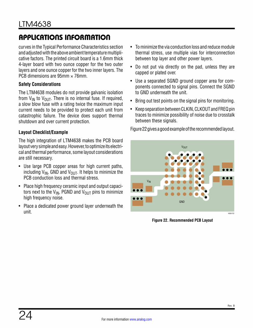
Layout Checklist/Example
The high integration of LTM4638 makes the PCB board layout very simple and easy. However, to optimize its electri-cal and thermal performance, some layout considerations are still necessary.
• Use large PCB copper areas for high current paths, including VIN, GND and VOUT. It helps to minimize the PCB conduction loss and thermal stress.
• Place high frequency ceramic input and output capaci-tors next to the VIN, PGND and VOUT pins to minimize high frequency noise.
• Place a dedicated power ground layer underneath the unit.
Figure 22. Recommended PCB Layout
VIN
VOUT
4638 F22
GND
• To minimize the via conduction loss and reduce module thermal stress, use multiple vias for interconnection between top layer and other power layers.
• Do not put via directly on the pad, unless they are capped or plated over.
• Use a separated SGND ground copper area for com-ponents connected to signal pins. Connect the SGND to GND underneath the unit.
• Bring out test points on the signal pins for monitoring.
• Keep separation between CLKIN, CLKOUT and FREQ pin traces to minimize possibility of noise due to crosstalk between these signals.
Figure 22 gives a good example of the recommended layout.
LTM4638
25Rev. B
For more information www.analog.com
APPLICATIONS INFORMATION
Figure 23. 3.1VIN to 20VIN, 1V Output at 15A Design
Figure 24. 5VIN to 20VIN, 3.3V Output with 2MHz External Clock
Figure 25. 3.1VIN to 20VIN, Two Phases, 1.5V at 30A Design
VIN
RUN
INTVCC
MODE/CLKIN
PHMODE
TRACK/SS
PGOOD
LTM4638
FREQ CLKOUTVOUT
VOSNS+22µF
25V 100µF6.3V×3
VIN3.1V TO 20V
VOUT1.0V15A
FB
COMPaCOMPb
GND
90.9k
33pF
VOSNS–
4638 F23
0.1µF
VIN
RUN
INTVCC
MODE/CLKIN
PHMODE
TRACK/SS
PGOOD
LTM4638
113k
CLKOUTFREQ
VOUT
VOSNS+22µF
25V 47µF6.3V×2
220µF6.3V
VIN5V TO 20V
VOUT3.3V15A
FB
COMPaCOMPb
GND
13.3k
VOSNS–
4638 F24
0.1µF
2MHz CLOCK
+
VIN
RUN
INTVCC
PHMODE
TRACK/SS
PGOOD
LTM4638
MODE/CLKIN VOUT
VOSNS+
VOSNS+
22µF25V×2 100µF
6.3V×6
33pF
40.2k
VIN3.1V TO 20V
VOUT1.5V30A
FB
COMPaCOMPb
GND
4638 F25
VOSNS–CLKOUT
FREQ
0.1µF
VIN
RUN
INTVCC
PHMODE
TRACK/SS
PGOOD
LTM4638
MODE/CLKIN
CLKOUTFREQVOUT
FB
COMPaCOMPb
GND VOSNS–
VOSNS+
LTM4638
26Rev. B
For more information www.analog.com
Figure 26. 3.1VIN to 20VIN, 1.2V and 1.5V with Coincident Tracking
APPLICATIONS INFORMATION
VIN
RUN
INTVCC
MODE/CLKIN
PHMODE
TRACK/SS
PGOOD
LTM4638
VOUT
VOSNS+22µF
25V×2
100µF6.3V×3
100µF6.3V×3
VIN3.1V TO 20V
VOUT1.5V15A
VOUT21.2V15A
FB
40.2k
33pF
COMPa
COMPb
GND
60.4k
60.4k
4638 F26
VOSNS–
FREQ CLKOUT
60.4k
0.1µF
VIN
RUN
INTVCC
MODE/CLKIN
PHMODE
TRACK/SS
PGOOD
LTM4638
VOUT
FB
COMPa
GND VOSNS–
FREQ CLKOUT
VOSNS+
33pF
COMPb
LTM4638
27Rev. B
For more information www.analog.com
PACKAGE DESCRIPTIONPACKAGE ROW AND COLUMN LABELING MAY VARY AMONG µModule PRODUCTS. REVIEW EACH PACKAGE LAYOUT CAREFULLY.
LTM4638 Component BGA Pinout
PIN ID FUNCTION PIN ID FUNCTION PIN ID FUNCTION PIN ID FUNCTION PIN ID FUNCTION PIN ID FUNCTION PIN ID FUNCTION
A1 VOUT A2 VOUT A3 VOUT A4 VOUT A5 VOUT A6 TSENSE+ A7 TSENSE–
B1 VOSNS+ B2 GND B3 INTVCC B4 RUN B5 PGOOD B6 GND B7 SW
C1 FB C2 VOSNS– C3 GND C4 GND C5 GND C6 GND C7 GND
D1 COMPa D2 MODE/CLKIN D3 VIN D4 VIN D5 GND D6 GND D7 GND
E1 FREQ E2 TRACK/SS E3 VIN E4 VIN E5 GND E6 GND E7 GND
F1 COMPb F2 CLKOUT F3 VOUT F4 VIN F5 GND F6 GND F7 GND
G1 VOUT G2 VOUT G3 VOUT G4 VIN G5 PHMODE G6 GND G7 GND
LTM4638
28Rev. B
For more information www.analog.com
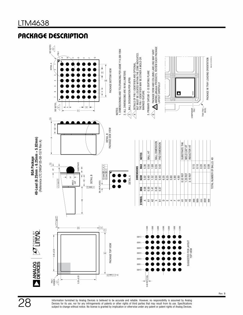
Information furnished by Analog Devices is believed to be accurate and reliable. However, no responsibility is assumed by Analog Devices for its use, nor for any infringements of patents or other rights of third parties that may result from its use. Specifications subject to change without notice. No license is granted by implication or otherwise under any patent or patent rights of Analog Devices.
PACKAGE DESCRIPTION
PACK
AGE
TOP
VIEW
4PIN
1CO
RNER
DETA
IL A
PACK
AGE
BOTT
OM V
IEW
3
SEE
NOTE
S
GFEDCBA
12
34
56
7
PIN
1
NOTE
S:1.
DIM
ENSI
ONIN
G AN
D TO
LERA
NCIN
G PE
R AS
ME
Y14.
5M-1
994
2. A
LL D
IMEN
SION
S AR
E IN
MIL
LIM
ETER
S
BAL
L DE
SIGN
ATIO
N PE
R JE
P95
43
DETA
ILS
OF P
IN 1
IDEN
TIFI
ER A
RE O
PTIO
NAL,
BUT
MUS
T BE
LOC
ATED
WIT
HIN
THE
ZONE
INDI
CATE
D.TH
E PI
N 1
IDEN
TIFI
ER M
AY B
E EI
THER
A M
OLD
OR
MAR
KED
FEAT
URE
A
DETA
IL B
PACK
AGE
SIDE
VIE
WA2
eb
eb
F
G
SUGG
ESTE
D PC
B LA
YOUT
TOP
VIEW
0.00
0
0.80
0
0.80
0
1.60
0
1.60
0
2.40
0
2.40
0
2.400
1.600
0.800
2.400
1.600
0.800
0.000
BGA
Pack
age
49-L
ead
(6.2
5mm
× 6
.25m
m ×
5.0
2mm
)(R
efer
ence
LTC
DW
G# 0
5-08
-157
4 Re
v A)
6
SEE
NOTE
S
DETA
IL A
Øb (4
9 PL
ACES
)
MX
YZ
ddd
MZ
eee
BGA
49 1
218
REV
A
TRAY
PIN
1BE
VEL
PACK
AGE
IN T
RAY
LOAD
ING
ORIE
NTAT
ION
X
aaa
Z2× D
5.28
±0.
20
Y
aaa Z 2×
E
5.48
±0.
20
0.40
REF
Ø 4
9x
SYM
BOL
A A1 A2 b b1 D E e F G H1 H2 H3 aaa
bbb
ccc
ddd
eee
MIN
4.68
0.30
1.41
0.45
0.37
NOM
5.02
0.40
1.52
0.50
0.40
6.25
6.25
0.80
4.80
4.80
0.32
REF
1.20
REF
3.10
REF
MAX
5.36
0.50
1.69
0.55
0.43
0.15
0.10
0.20
0.20
0.08
TOTA
L NU
MBE
R OF
BAL
LS: 4
9
DIM
ENSI
ONS
NOTE
S
BALL
HT
BALL
DIM
ENSI
ONPA
D DI
MEN
SION
SUBS
TRAT
E TH
KM
OLD
CAP
HTIN
DUCT
OR H
T
Z
5. P
RIM
ARY
DATU
M -Z
- IS
SEAT
ING
PLAN
E
6PA
CKAG
E RO
W A
ND C
OLUM
N LA
BELI
NG M
AY V
ARY
AMON
G µM
odul
e PR
ODUC
TS. R
EVIE
W E
ACH
PACK
AGE
LAYO
UT C
AREF
ULLY
!
DETA
IL B
SUBS
TRAT
E
A1
ccc
Z
// bbb Z
H2H1
H3
b1M
OLD
CAP
Z
COM
PONE
NTPI
N 1
LTM4638
29Rev. B
For more information www.analog.com
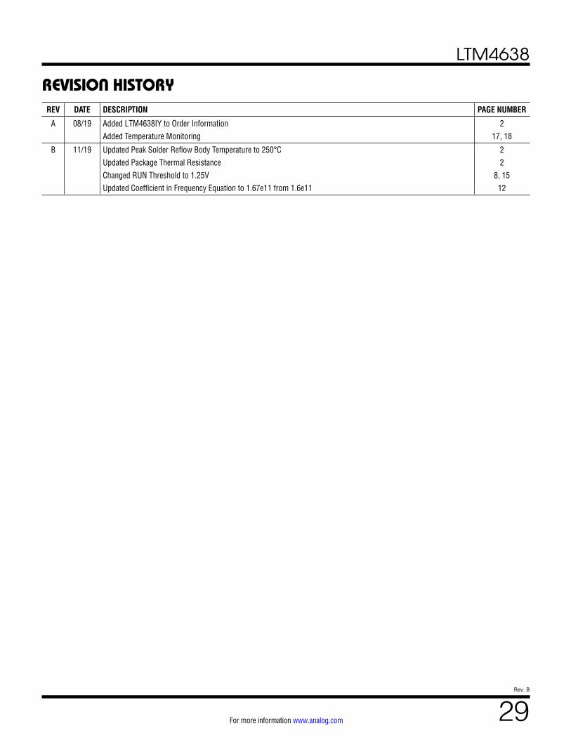
REVISION HISTORYREV DATE DESCRIPTION PAGE NUMBER
A 08/19 Added LTM4638IY to Order InformationAdded Temperature Monitoring
217, 18
B 11/19 Updated Peak Solder Reflow Body Temperature to 250°CUpdated Package Thermal ResistanceChanged RUN Threshold to 1.25VUpdated Coefficient in Frequency Equation to 1.67e11 from 1.6e11
22
8, 1512

LTM4638
30Rev. B
For more information www.analog.com ANALOG DEVICES, INC. 2018–2019
11/19www.analog.com
RELATED PARTS
PACKAGE PHOTO
PART NUMBER DESCRIPTION COMMENTSLTM4626 12A µModule Regulator. Pin Compatible with
LTM4638.3.1V ≤ VIN ≤ 20V. 0.6V ≤ VOUT ≤ 5.5V. 6.25mm × 6.25mm × 3.87mm BGA
LTM4649 10A µModule Regulator 4.5V ≤ VIN ≤ 16V. 0.6V ≤ VOUT ≤ 3.3V. 9mm × 15mm × 4.92mm BGALTM4601 12A µModule Regulator 4.5V ≤ VIN ≤ 20V (28V LTM4601HV). 0.5V ≤ VOUT ≤ 5V. 15mm × 15mm ×
2.82mm LGA. 15mm × 15mm × 3.42mm BGALTM4637 20A µModule Regulator 4.5V ≤ VIN ≤ 20V. 0.6V ≤ VOUT ≤ 5.5V. 15mm × 15mm × 4.32mm LGA. 15mm ×
15mm × 4.92mm BGA.LTM4646 Dual 10A µModule Regulator 4.5V ≤ VIN ≤ 20V. 0.6V ≤ VOUT ≤ 5.5V. 11.25mm × 15mm × 5.01mm BGALTM4662 Dual 15A µModule Regulator 4.5V ≤ VIN ≤ 20V. 0.6V ≤ VOUT ≤ 5.5V. 11.25mm × 15mm × 5.74mm BGALTM4643 Quad 3A Ultrathin µModule Regulator 4V ≤ VIN ≤ 20V. 0.6V ≤ VOUT ≤ 3.3V. 9mm × 15mm × 1.82mm LGA. 9mm ×
15mm × 2.42mm BGALTM4644 Quad 4A µModule Regulator 4V ≤ VIN ≤ 14V. 0.6V ≤ VOUT ≤ 5.5V. 9mm × 15mm × 5.01mm BGA
DESIGN RESOURCES
SUBJECT DESCRIPTION
µModule Design and Manufacturing Resources Design: • Selector Guides • Demo Boards and Gerber Files • Free Simulation Tools
Manufacturing: • Quick Start Guide • PCB Design, Assembly and Manufacturing Guidelines • Package and Board Level Reliability
µModule Regulator Products Search 1. Sort table of products by parameters and download the result as a spread sheet.2. Search using the Quick Power Search parametric table.
Digital Power System Management Analog Devices’ family of digital power supply management ICs are highly integrated solutions that offer essential functions, including power supply monitoring, supervision, margining and sequencing, and feature EEPROM for storing user configurations and fault logging.