ltm8032 - en55022b compliant 36v, 2a dc/dc µmodule...
TRANSCRIPT

LTM8032
18032fg
For more information www.linear.com/LTM8032
Typical applicaTion
DescripTion
EN55022B Compliant 36V, 2A DC/DC µModule
Regulator
The LTM®8032 is an electromagnetic compatible (EMC) 36V, 2A DC/DC step-down µModule® regulator designed to meet the radiated emissions requirements of EN55022. Conducted emission requirements can be met by adding standard filter components. Included in the package are the switching controller, power switches, inductor, filters and all support components. Operating over an input voltage range of 3.6V to 36V, the LTM8032 supports an output voltage range of 0.8V to 10V, and a switching frequency range of 200kHz to 2.4MHz, each set by a single resistor. Only the bulk input and output filter capacitors are needed to finish the design. The low profile package enables uti-lization of unused space on the bottom of PC boards for high density point of load regulation.
The LTM8032 is packaged in a thermally enhanced, com-pact and low profile overmolded land grid array (LGA) and ball grid array (BGA) packages suitable for automated assembly by standard surface mount equipment. The LTM8032 is available with SnPb (BGA) or RoHS compli-ant terminal finish.L, LT, LTC, LTM, Linear Technology, the Linear logo, µModule and Burst Mode are registered trademarks of Linear Technology Corporation. All other trademarks are the property of their respective owners.
Ultralow Noise 5V/2A DC/DC µModule Regulator
FeaTures
applicaTions
n Complete Step-Down Switch Mode Power Supplyn Wide Input Voltage Range: 3.6V to 36Vn 2A Output Currentn 0.8V to 10V Output Voltagen Selectable Switching Frequency: 200kHz to 2.4MHzn EN55022 Class B Compliantn Current Mode Controln Programmable Soft-Startn SnPb (BGA) or RoHS Compliant (LGA and BGA)
Finishn Low Profile, Surface Mount LGA (9mm × 15mm
× 2.82mm) and BGA (9mm × 15mm × 3.42mm) Packages
n Automotive Battery Regulationn Power for Portable Productsn Distributed Supply Regulationn Industrial Suppliesn Wall Transformer Regulation
LTM8032 EMI Performance
90
70
50
EMIS
SION
S LE
VEL
(dBµ
V/m
)
30
10
80
60
40
20
0
–100 100 200 300 400 500
FREQUENCY (MHz)600 700 800 900 1000
EN55022CLASS BLIMIT
8031 TA01b
RT
SHARE
47.5k44.2k
fSW = 700kHz
*RUNNING VOLTAGE RANGE. SEE APPLICATIONS FOR START-UP DETAILS
VIN
FIN
2.2µF
10µF
VOUT5V2A
RUN/SS
VIN*7VDC TO 36VDC
PGOOD
BIASLTM8032
AUX
VOUT
SYNC GND
8032 TA01a
ADJ
LTM8032
28032fg
For more information www.linear.com/LTM8032
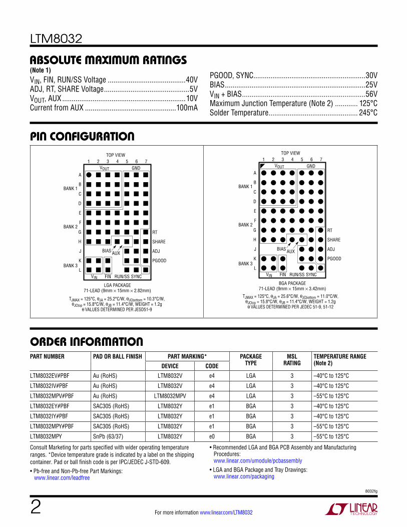
VIN, FIN, RUN/SS Voltage .........................................40VADJ, RT, SHARE Voltage .............................................5VVOUT, AUX .................................................................10VCurrent from AUX ................................................100mA
(Note 1)
GND1
A
B
CBANK 1
BANK 2
BANK 3
D
E
F
G
H
J
K
L
2 3 4TOP VIEW
LGA PACKAGE71-LEAD (9mm × 15mm × 2.82mm)
5 6 7VOUT
VIN
RT
SHARE
ADJ
PGOOD
SYNCRUN/SSFIN
BIAS AUX
TJMAX = 125°C, θJA = 25.2°C/W, θJCbottom = 10.3°C/W, θJCtop = 15.8°C/W, θJB = 11.4°C/W, WEIGHT = 1.2g
θ VALUES DETERMINED PER JESD51-9
GND1
A
B
CBANK 1
BANK 2
BANK 3
D
E
F
G
H
J
K
L
2 3 4TOP VIEW
BGA PACKAGE71-LEAD (9mm × 15mm × 3.42mm)
5 6 7VOUT
VIN
RT
SHARE
ADJ
PGOOD
SYNCRUN/SSFIN
BIAS AUX
TJMAX = 125°C, θJA = 25.6°C/W, θJCbottom = 11.0°C/W, θJCtop = 15.8°C/W, θJB = 11.4°C/W, WEIGHT = 1.2g
θ VALUES DETERMINED PER JEDEC 51-9, 51-12
pin conFiguraTion
absoluTe MaxiMuM raTings
PART NUMBER PAD OR BALL FINISH PART MARKING* PACKAGE TYPE
MSL RATING
TEMPERATURE RANGE (Note 2)DEVICE CODE
LTM8032EV#PBF Au (RoHS) LTM8032V e4 LGA 3 –40°C to 125°C
LTM8032IV#PBF Au (RoHS) LTM8032V e4 LGA 3 –40°C to 125°C
LTM8032MPV#PBF Au (RoHS) LTM8032MPV e4 LGA 3 –55°C to 125°C
LTM8032EY#PBF SAC305 (RoHS) LTM8032Y e1 BGA 3 –40°C to 125°C
LTM8032IY#PBF SAC305 (RoHS) LTM8032Y e1 BGA 3 –40°C to 125°C
LTM8032MPY#PBF SAC305 (RoHS) LTM8032Y e1 BGA 3 –55°C to 125°C
LTM8032MPY SnPb (63/37) LTM8032Y e0 BGA 3 –55°C to 125°C
orDer inForMaTion
PGOOD, SYNC...........................................................30VBIAS ..........................................................................25VVIN + BIAS .................................................................56VMaximum Junction Temperature (Note 2) ............ 125°CSolder Temperature ............................................... 245°C
Consult Marketing for parts specified with wider operating temperature ranges. *Device temperature grade is indicated by a label on the shipping container. Pad or ball finish code is per IPC/JEDEC J-STD-609.• Pb-free and Non-Pb-free Part Markings:
www.linear.com/leadfree
• Recommended LGA and BGA PCB Assembly and Manufacturing Procedures: www.linear.com/umodule/pcbassembly
• LGA and BGA Package and Tray Drawings: www.linear.com/packaging
LTM8032
38032fg
For more information www.linear.com/LTM8032
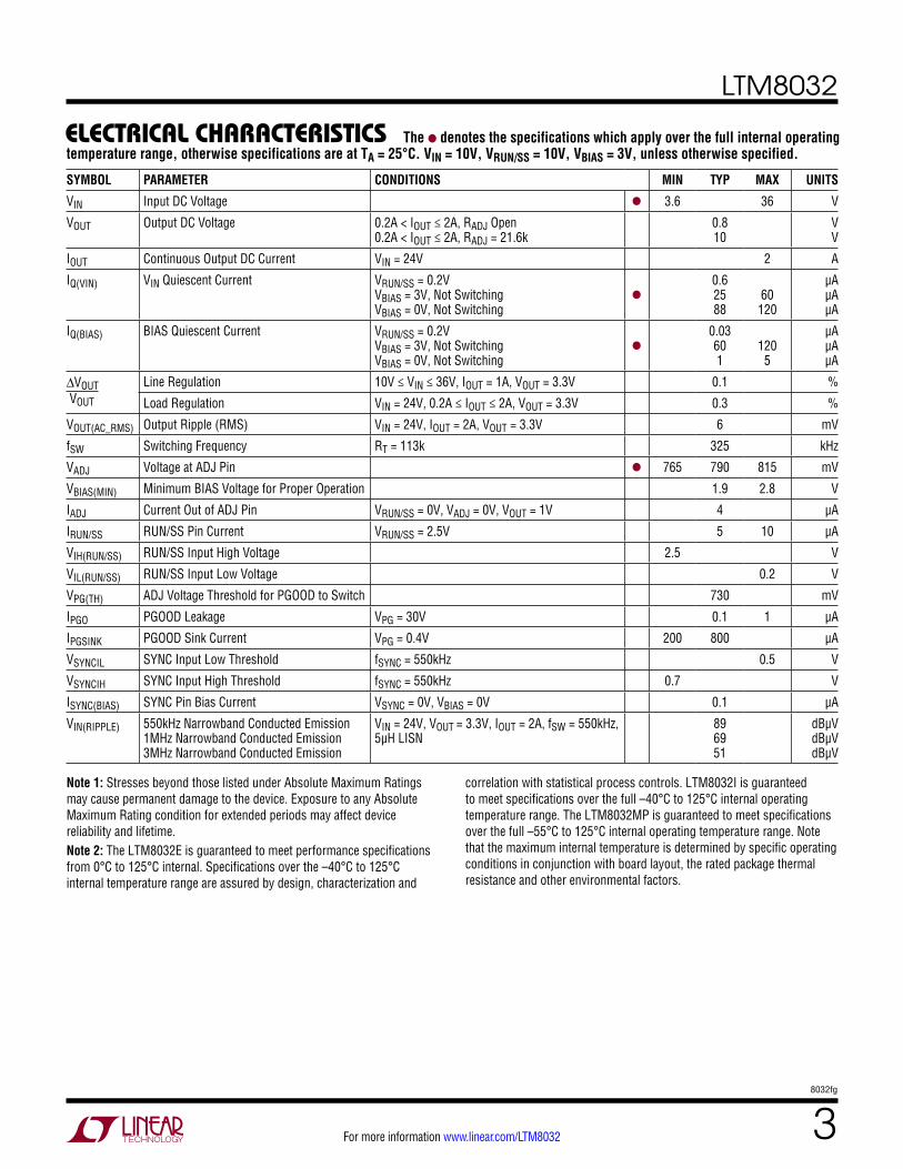
elecTrical characTerisTics
Note 1: Stresses beyond those listed under Absolute Maximum Ratings may cause permanent damage to the device. Exposure to any Absolute Maximum Rating condition for extended periods may affect device reliability and lifetime.Note 2: The LTM8032E is guaranteed to meet performance specifications from 0°C to 125°C internal. Specifications over the –40°C to 125°C internal temperature range are assured by design, characterization and
The l denotes the specifications which apply over the full internal operating temperature range, otherwise specifications are at TA = 25°C. VIN = 10V, VRUN/SS = 10V, VBIAS = 3V, unless otherwise specified.
SYMBOL PARAMETER CONDITIONS MIN TYP MAX UNITS
VIN Input DC Voltage l 3.6 36 V
VOUT Output DC Voltage 0.2A < IOUT ≤ 2A, RADJ Open 0.2A < IOUT ≤ 2A, RADJ = 21.6k
0.8 10
V V
IOUT Continuous Output DC Current VIN = 24V 2 A
IQ(VIN) VIN Quiescent Current VRUN/SS = 0.2V VBIAS = 3V, Not Switching VBIAS = 0V, Not Switching
l
0.6 25 88
60
120
µA µA µA
IQ(BIAS) BIAS Quiescent Current VRUN/SS = 0.2V VBIAS = 3V, Not Switching VBIAS = 0V, Not Switching
l
0.03 60 1
120
5
µA µA µA
∆VOUT VOUT
Line Regulation 10V ≤ VIN ≤ 36V, IOUT = 1A, VOUT = 3.3V 0.1 %
Load Regulation VIN = 24V, 0.2A ≤ IOUT ≤ 2A, VOUT = 3.3V 0.3 %
VOUT(AC_RMS) Output Ripple (RMS) VIN = 24V, IOUT = 2A, VOUT = 3.3V 6 mV
fSW Switching Frequency RT = 113k 325 kHz
VADJ Voltage at ADJ Pin l 765 790 815 mV
VBIAS(MIN) Minimum BIAS Voltage for Proper Operation 1.9 2.8 V
IADJ Current Out of ADJ Pin VRUN/SS = 0V, VADJ = 0V, VOUT = 1V 4 µA
IRUN/SS RUN/SS Pin Current VRUN/SS = 2.5V 5 10 µA
VIH(RUN/SS) RUN/SS Input High Voltage 2.5 V
VIL(RUN/SS) RUN/SS Input Low Voltage 0.2 V
VPG(TH) ADJ Voltage Threshold for PGOOD to Switch 730 mV
IPGO PGOOD Leakage VPG = 30V 0.1 1 µA
IPGSINK PGOOD Sink Current VPG = 0.4V 200 800 µA
VSYNCIL SYNC Input Low Threshold fSYNC = 550kHz 0.5 V
VSYNCIH SYNC Input High Threshold fSYNC = 550kHz 0.7 V
ISYNC(BIAS) SYNC Pin Bias Current VSYNC = 0V, VBIAS = 0V 0.1 µA
VIN(RIPPLE) 550kHz Narrowband Conducted Emission 1MHz Narrowband Conducted Emission 3MHz Narrowband Conducted Emission
VIN = 24V, VOUT = 3.3V, IOUT = 2A, fSW = 550kHz, 5µH LISN
89 69 51
dBµV dBµV dBµV
correlation with statistical process controls. LTM8032I is guaranteed to meet specifications over the full –40°C to 125°C internal operating temperature range. The LTM8032MP is guaranteed to meet specifications over the full –55°C to 125°C internal operating temperature range. Note that the maximum internal temperature is determined by specific operating conditions in conjunction with board layout, the rated package thermal resistance and other environmental factors.
LTM8032
48032fg
For more information www.linear.com/LTM8032
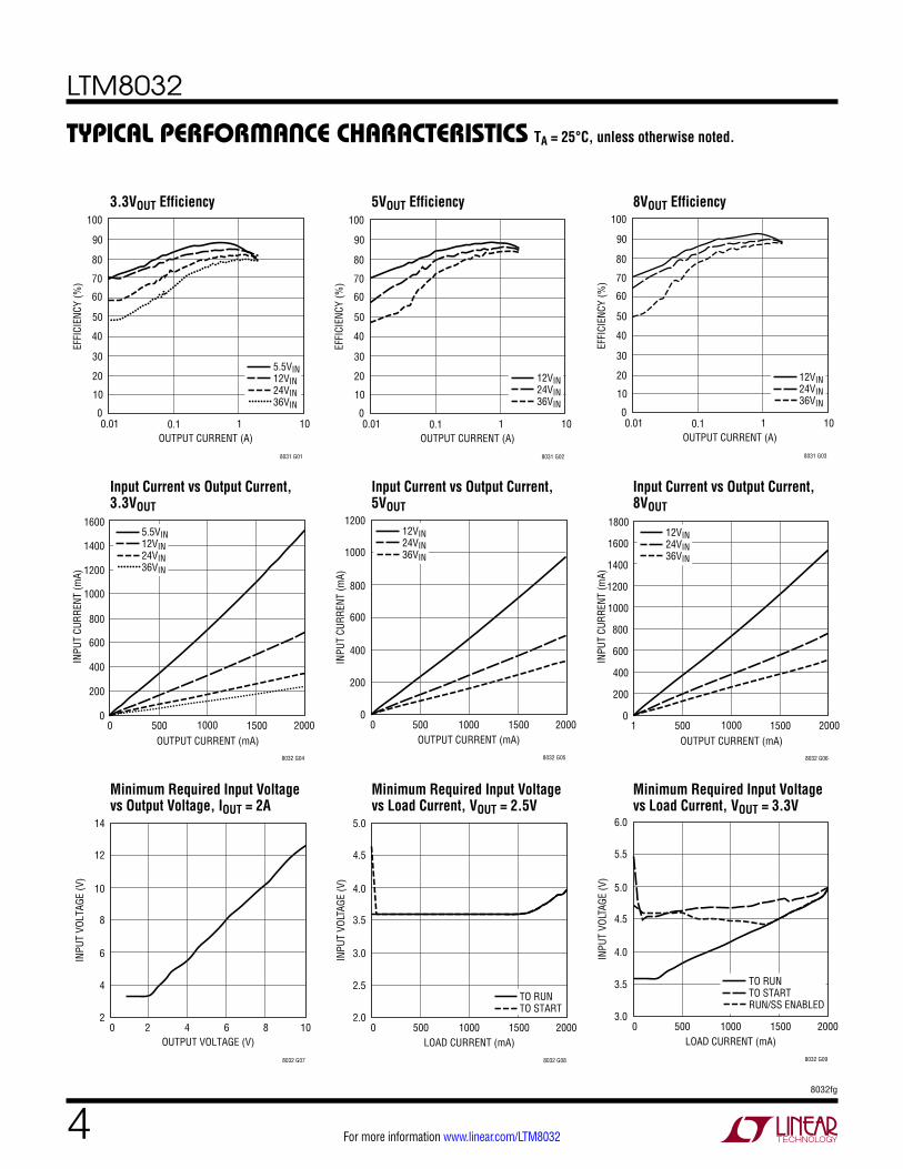
Typical perForMance characTerisTics
Input Current vs Output Current, 3.3VOUT
Input Current vs Output Current, 5VOUT
Input Current vs Output Current, 8VOUT
Minimum Required Input Voltage vs Output Voltage, IOUT = 2A
Minimum Required Input Voltage vs Load Current, VOUT = 2.5V
Minimum Required Input Voltage vs Load Current, VOUT = 3.3V
3.3VOUT Efficiency 5VOUT Efficiency 8VOUT Efficiency
TA = 25°C, unless otherwise noted.
OUTPUT CURRENT (A)0.01
0
EFFI
CIEN
CY (%
)
20
30
40
50
60
70
0.1 1
8031 G01
80
90
100
10
10
5.5VIN12VIN24VIN36VIN
OUTPUT CURRENT (A)0.01
0
EFFI
CIEN
CY (%
)
20
30
40
50
60
70
0.1 1
8031 G02
80
90
100
10
10
12VIN24VIN36VIN
OUTPUT CURRENT (A)0.01
0
EFFI
CIEN
CY (%
)
20
30
40
50
60
70
0.1 1
8031 G03
80
90
100
10
10
12VIN24VIN36VIN
OUTPUT CURRENT (mA)0
INPU
T CU
RREN
T (m
A)
800
1000
1200
2000
8032 G04
600
400
0500 1000 1500
200
1600
14005.5VIN12VIN24VIN36VIN
OUTPUT CURRENT (mA)0
0
INPU
T CU
RREN
T (m
A)
200
400
600
800
1000
1200
500 1000 1500 2000
8032 G05
12VIN24VIN36VIN
OUTPUT CURRENT (mA)1
INPU
T CU
RREN
T (m
A)1000
1200
1400
2000
8032 G06
800
600
0500 1000 1500
400
200
1800
160012VIN24VIN36VIN
OUTPUT VOLTAGE (V)0
2
INPU
T VO
LTAG
E (V
)
4
6
8
10
12
14
2 4 6 8
8032 G07
10LOAD CURRENT (mA)
02.0
INPU
T VO
LTAG
E (V
)
2.5
3.0
3.5
4.0
4.5
5.0
500 1000 1500 2000
8032 G08
TO RUNTO START
LOAD CURRENT (mA)0
3.0
INPU
T VO
LTAG
E (V
)
3.5
4.0
4.5
5.0
5.5
6.0
500 1000 1500 2000
8032 G09
TO RUNTO STARTRUN/SS ENABLED
LTM8032
58032fg
For more information www.linear.com/LTM8032
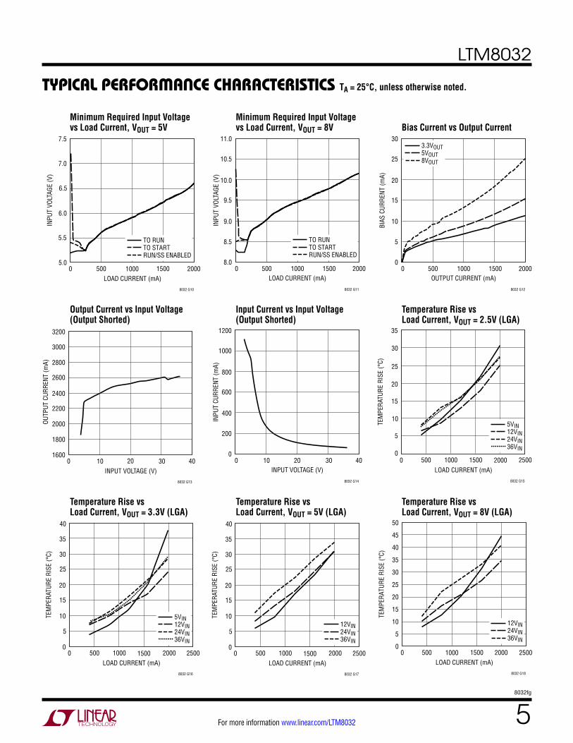
Typical perForMance characTerisTics
Output Current vs Input Voltage (Output Shorted)
Input Current vs Input Voltage (Output Shorted)
Temperature Rise vs Load Current, VOUT = 2.5V (LGA)
Temperature Rise vs Load Current, VOUT = 3.3V (LGA)
Temperature Rise vs Load Current, VOUT = 5V (LGA)
Temperature Rise vs Load Current, VOUT = 8V (LGA)
Minimum Required Input Voltage vs Load Current, VOUT = 5V
Minimum Required Input Voltage vs Load Current, VOUT = 8V Bias Current vs Output Current
TA = 25°C, unless otherwise noted.
LOAD CURRENT (mA)0
INPU
T VO
LTAG
E (V
)
6.5
7.0
7.5
8032 G10
6.0
5.5
5.0500 1000 1500 2000
TO RUNTO STARTRUN/SS ENABLED
LOAD CURRENT (mA)0
8.0
INPU
T VO
LTAG
E (V
)
8.5
9.0
9.5
10.0
10.5
11.0
500 1000 1500 2000
8032 G11
TO RUNTO STARTRUN/SS ENABLED
OUTPUT CURRENT (mA)0
0
BIAS
CUR
RENT
(mA)
5
10
15
20
25
30
500 1000 1500 2000
8032 G12
3.3VOUT5VOUT8VOUT
INPUT VOLTAGE (V)0
OUTP
UT C
URRE
NT (m
A)
2400
2600
2800
40
8032 G13
2200
2000
160010 20 30
1800
3200
3000
INPUT VOLTAGE (V)0
0
INPU
T CU
RREN
T (m
A)
200
400
600
800
1000
1200
10 20 30 40
8032 G14
LOAD CURRENT (mA)0
25
30
35
2000
8032 G15
20
15
500 1000 1500 2500
10
5
0
TEM
PERA
TURE
RIS
E (°
C)
5VIN12VIN24VIN36VIN
LOAD CURRENT (mA)0
TEM
PERA
TURE
RIS
E (°
C)
15
20
25
1500 2500
8032 G16
10
5
0500 1000 2000
30
35
40
5VIN12VIN24VIN36VIN
LOAD CURRENT (mA)0
TEM
PERA
TURE
RIS
E (°
C)
15
20
25
1500 2500
8032 G17
10
5
0500 1000 2000
30
35
40
12VIN24VIN36VIN
LOAD CURRENT (mA)0
TEM
PERA
TURE
RIS
E (°
C)
30
40
50
2000
8032 G18
20
10
25
35
45
15
5
0500 1000 1500 2500
12VIN24VIN36VIN
LTM8032
68032fg
For more information www.linear.com/LTM8032
Typical perForMance characTerisTics
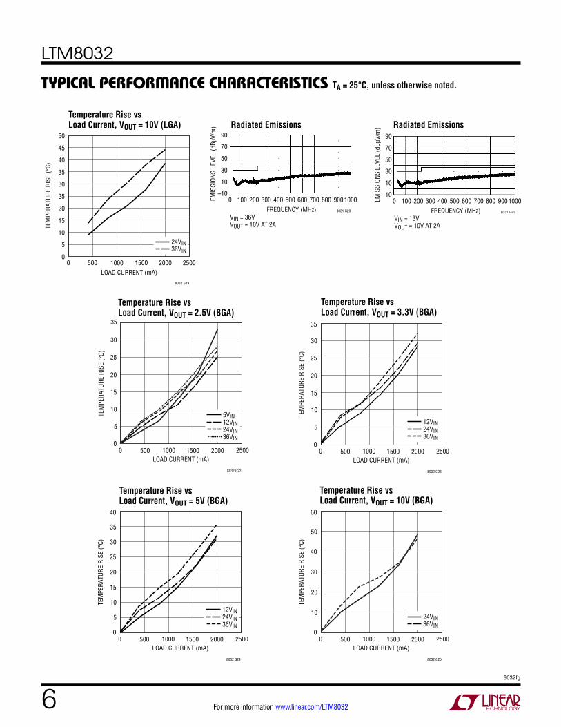
Temperature Rise vs Load Current, VOUT = 10V (LGA) Radiated Emissions Radiated Emissions
TA = 25°C, unless otherwise noted.
Temperature Rise vs Load Current, VOUT = 2.5V (BGA)
Temperature Rise vs Load Current, VOUT = 5V (BGA)
Temperature Rise vs Load Current, VOUT = 3.3V (BGA)
Temperature Rise vs Load Current, VOUT = 10V (BGA)
LOAD CURRENT (mA)0
TEM
PERA
TURE
RIS
E (°
C)
30
40
50
2000
8032 G19
20
10
25
35
45
15
5
0500 1000 1500 2500
24VIN36VIN
90
70
50
EMIS
SION
S LE
VEL
(dBµ
V/m
)
30
10
–100
VIN = 36VVOUT = 10V AT 2A
100 200 300 400 500FREQUENCY (MHz)
600 700 800 900 1000
8031 G20
90
70
50
EMIS
SION
S LE
VEL
(dBµ
V/m
)
30
10
–100
VIN = 13VVOUT = 10V AT 2A
100 200 300 400 500FREQUENCY (MHz)
600 700 800 900 1000
8031 G21
LOAD CURRENT (mA)0
0
TEM
PERA
TURE
RIS
E (°
C)
10
15
20
25
500 1500 20001000
8032 G22
30
35
5
2500
5VIN12VIN24VIN36VIN
LOAD CURRENT (mA)0
0
TEM
PERA
TURE
RIS
E (°
C)
15
20
500 1500 20001000
8032 G23
25
30
35
10
5
2500
12VIN24VIN36VIN
LOAD CURRENT (mA)0
0
TEM
PERA
TURE
RIS
E (°
C)
15
20
500 1500 20001000
8032 G24
25
35
30
40
10
5
2500
12VIN24VIN36VIN
LOAD CURRENT (mA)0
0
TEM
PERA
TURE
RIS
E (°
C)
30
500 1500 20001000
8032 G25
40
50
60
20
10
2500
24VIN36VIN

LTM8032
78032fg
For more information www.linear.com/LTM8032
pin FuncTionsVIN (Bank 3): The VIN pin supplies current to the LTM8032’s internal regulator and to the internal power switch. This pin must be locally bypassed with an external, low ESR capacitor of at least 2.2µF.
FIN (K3, L3): Filtered Input. This is the node after the input EMI filter. Use this only if there is a need to modify the behavior of the integrated EMI filter or if VIN rises or falls rapidly; otherwise, leave these pins unconnected. See the Applications Information section for more details.
GND (Bank 2): Tie these GND pins to a local ground plane below the LTM8032 and the circuit components. In most applications, the bulk of the heat flow out of the LTM8032 is through these pads, so the printed circuit design has a large impact on the thermal performance of the part. See the PCB Layout and Thermal Considerations sections for more details. Return the feedback divider (RADJ) to this net.
VOUT (Bank 1): Power Output Pins. Apply the output filter capacitor and the output load between these pins and GND pins.
AUX (Pin H5): Low Current Voltage Source for BIAS. The AUX pin is internally connected to VOUT and is placed adjacent to the BIAS pin to ease printed circuit board routing. Although this pin is internally connected to VOUT, do not connect this pin to the load. If this pin is not tied to BIAS, leave it floating.
BIAS (Pin H4): The BIAS pin connects to the internal power bus. Connect to a power source greater than 2.8V. If the output is greater than 2.8V, connect this pin to AUX. If the output voltage is less, connect this to a voltage source between 2.8V and 25V. Also, make sure that BIAS + VIN is less than 56V.
RUN/SS (Pin L5): Pull RUN/SS pin to less than 0.2V to shut down the LTM8032. Tie to 2.5V or more for normal operation. If the shutdown feature is not used, tie this pin to the VIN pin. RUN/SS also provides a soft-start function; see the Applications Information section.
RT (Pin G7): The RT pin is used to program the switching frequency of the LTM8032 by connecting a resistor from this pin to ground. The Applications Information section of the data sheet includes a table to determine the resistance value based on the desired switching frequency. Minimize capacitance at this pin.
SHARE (Pin H7): Tie this to the SHARE pin of another LTM8032 when paralleling the outputs. Otherwise, do not connect (leave floating).
SYNC (Pin L6): This is the external clock synchronization input. Ground this pin for low ripple Burst Mode® operation at low output loads. Tie to a stable voltage source greater than 0.7V to disable Burst Mode operation. Do not leave this pin floating. Tie to a clock source for synchronization. Clock edges should have rise and fall times faster than 1µs. See synchronization section in Applications Information.
PGOOD (Pin K7): The PGOOD pin is the open-collector output of an internal comparator. PGOOD remains low until the ADJ pin is within 10% of the final regulation voltage. The PGOOD output is valid when VIN is above 3.6V and RUN/SS is high. If this function is not used, leave this pin floating.
ADJ (Pin J7): The LTM8032 regulates its ADJ pin to 0.79V. Connect the adjust resistor from this pin to ground. The value of RADJ is given by the equation:
RADJ =
196.71VOUT – 0.79
where RADJ is in kΩ.
LTM8032
88032fg
For more information www.linear.com/LTM8032
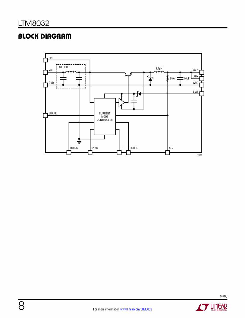
block DiagraM
CURRENTMODE
CONTROLLER
249k 10µF
VOUT
AUX
GND
4.7µH
BIAS
EMI FILTER
FIN
VIN
GND
SHARE
SYNC RT PGOOD ADJ
8032 BD
RUN/SS
LTM8032
98032fg
For more information www.linear.com/LTM8032
operaTion
applicaTions inForMaTion
The LTM8032 is a standalone nonisolated step-down switching DC/DC power supply. It can deliver up to 2A of DC output current with only bulk external input and output capacitors. This module provides a precisely regulated output voltage programmable via one external resistor from 0.8VDC to 10VDC. The input voltage range is 3.6V to 36V. Given that the LTM8032 is a step-down converter, make sure that the input voltage is high enough to support the desired output voltage and load current. A simplified Block Diagram is given on the previous page.
The LTM8032 is designed with an input EMI filter and other features to make its radiated emissions compliant with several EMC specifications including EN55022 class B. Compliance with conducted emissions requirements may be obtained by adding a standard input filter.
The LTM8032 contains a current mode controller, power switching element, power inductor, power Schottky diode and a modest amount of input and output capacitance. The LTM8032 is a fixed frequency PWM regulator. The switching frequency is set by simply connecting the ap-propriate resistor value from the RT pin to GND.
An internal regulator provides power to the control circuitry. The bias regulator can draw power from the VIN pin, but if the BIAS pin is connected to an external voltage higher than 2.8V, bias power will be drawn from the external source (typically the regulated output voltage). This improves efficiency. The RUN/SS pin is used to place the LTM8032 in shutdown, disconnecting the output and reducing the input current to less than 1µA.
To further optimize efficiency, the LTM8032 automatically switches to Burst Mode operation in light load situations. Between bursts, all circuitry associated with controlling the output switch is shut down reducing the input supply current to 50µA in a typical application. The oscillator reduces the LTM8032’s operating frequency when the voltage at the ADJ pin is low. This frequency foldback helps to control the output current during start-up and overload.
The LTM8032 contains a power good comparator which trips when the ADJ pin is at 90% of its regulated value. The PGOOD output is an open-collector transistor that is off when the output is in regulation, allowing an external resistor to pull the PGOOD pin high. Power good is valid when the LTM8032 is enabled and VIN is above 3.6V.
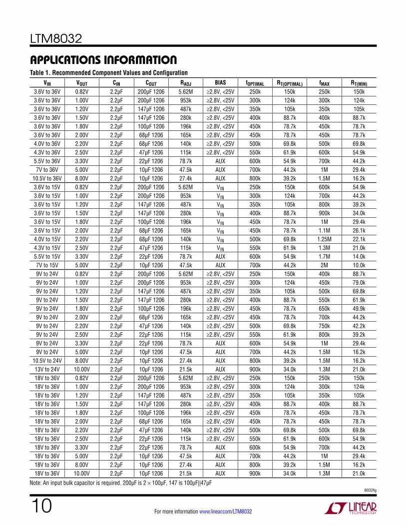
For most applications, the design process is straight forward, summarized as follows:
1. Look at Table 1 and find the row that has the desired input range and output voltage.
2. Apply the recommended CIN, COUT, RADJ and RT values.
3. Connect BIAS as indicated.
As the integrated input EMI filter may ring in response to an application of a step input voltage, a bulk capacitance, series resistance or some clamping mechanism may be required. See the Hot-Plugging Safely section for details.
While these component combinations have been tested for proper operation, it is incumbent upon the user to verify proper operation over the intended system’s line, load and environmental conditions.
Capacitor Selection Considerations
The CIN and COUT capacitor values in Table 1 are the minimum recommended values for the associated oper-ating conditions. Applying capacitor values below those indicated in Table 1 is not recommended, and may result in undesirable operation. Using larger values is generally acceptable, and can yield improved dynamic response, if it is necessary. Again, it is incumbent upon the user to verify proper operation over the intended system’s line, load and environmental conditions.
Ceramic capacitors are small, robust and have very low ESR. However, not all ceramic capacitors are suitable. X5R and X7R types are stable over temperature and ap-plied voltage and give dependable service. Other types, including Y5V and Z5U have very large temperature and voltage coefficients of capacitance. In an application
LTM8032
108032fg
For more information www.linear.com/LTM8032
applicaTions inForMaTionTable 1. Recommended Component Values and Configuration
VIN VOUT CIN COUT RADJ BIAS fOPTIMAL RT(OPTIMAL) fMAX RT(MIN)
3.6V to 36V 0.82V 2.2µF 200µF 1206 5.62M ≥2.8V, <25V 250k 150k 250k 150k3.6V to 36V 1.00V 2.2µF 200µF 1206 953k ≥2.8V, <25V 300k 124k 300k 124k3.6V to 36V 1.20V 2.2µF 147µF 1206 487k ≥2.8V, <25V 350k 105k 350k 105k3.6V to 36V 1.50V 2.2µF 147µF 1206 280k ≥2.8V, <25V 400k 88.7k 400k 88.7k3.6V to 36V 1.80V 2.2µF 100µF 1206 196k ≥2.8V, <25V 450k 78.7k 450k 78.7k3.6V to 36V 2.00V 2.2µF 68µF 1206 165k ≥2.8V, <25V 450k 78.7k 450k 78.7k4.0V to 36V 2.20V 2.2µF 68µF 1206 140k ≥2.8V, <25V 500k 69.8k 500k 69.8k4.3V to 36V 2.50V 2.2µF 47µF 1206 115k ≥2.8V, <25V 550k 61.9k 600k 54.9k5.5V to 36V 3.30V 2.2µF 22µF 1206 78.7k AUX 600k 54.9k 700k 44.2k7V to 36V 5.00V 2.2µF 10µF 1206 47.5k AUX 700k 44.2k 1M 29.4k
10.5V to 36V 8.00V 2.2µF 10µF 1206 27.4k AUX 800k 39.2k 1.5M 16.2k3.6V to 15V 0.82V 2.2µF 200µF 1206 5.62M VIN 250k 150k 600k 54.9k3.6V to 15V 1.00V 2.2µF 200µF 1206 953k VIN 300k 124k 700k 44.2k3.6V to 15V 1.20V 2.2µF 147µF 1206 487k VIN 350k 105k 800k 39.2k3.6V to 15V 1.50V 2.2µF 147µF 1206 280k VIN 400k 88.7k 900k 34.0k3.6V to 15V 1.80V 2.2µF 100µF 1206 196k VIN 450k 78.7k 1M 29.4k3.6V to 15V 2.00V 2.2µF 68µF 1206 165k VIN 450k 78.7k 1.1M 26.1k4.0V to 15V 2.20V 2.2µF 68µF 1206 140k VIN 500k 69.8k 1.25M 22.1k4.3V to 15V 2.50V 2.2µF 47µF 1206 115k VIN 550k 61.9k 1.3M 21.0k5.5V to 15V 3.30V 2.2µF 22µF 1206 78.7k AUX 600k 54.9k 1.7M 14.0k7V to 15V 5.00V 2.2µF 10µF 1206 47.5k AUX 700k 44.2k 2M 10.0k9V to 24V 0.82V 2.2µF 200µF 1206 5.62M ≥2.8V, <25V 250k 150k 400k 88.7k9V to 24V 1.00V 2.2µF 200µF 1206 953k ≥2.8V, <25V 300k 124k 450k 79.0k9V to 24V 1.20V 2.2µF 147µF 1206 487k ≥2.8V, <25V 350k 105k 500k 69.8k9V to 24V 1.50V 2.2µF 147µF 1206 280k ≥2.8V, <25V 400k 88.7k 550k 61.9k9V to 24V 1.80V 2.2µF 100µF 1206 196k ≥2.8V, <25V 450k 78.7k 650k 49.9k9V to 24V 2.00V 2.2µF 68µF 1206 165k ≥2.8V, <25V 450k 78.7k 700k 44.2k9V to 24V 2.20V 2.2µF 47µF 1206 140k ≥2.8V, <25V 500k 69.8k 750k 42.2k9V to 24V 2.50V 2.2µF 22µF 1206 115k ≥2.8V, <25V 550k 61.9k 800k 39.2k9V to 24V 3.30V 2.2µF 22µF 1206 78.7k AUX 600k 54.9k 1M 29.4k9V to 24V 5.00V 2.2µF 10µF 1206 47.5k AUX 700k 44.2k 1.5M 16.2k
10.5V to 24V 8.00V 2.2µF 10µF 1206 27.4k AUX 800k 39.2k 1.5M 16.2k13V to 24V 10.00V 2.2µF 10µF 1206 21.5k AUX 900k 34.0k 1.3M 21.0k18V to 36V 0.82V 2.2µF 200µF 1206 5.62M ≥2.8V, <25V 250k 150k 250k 150k18V to 36V 1.00V 2.2µF 200µF 1206 953k ≥2.8V, <25V 300k 124k 300k 124k18V to 36V 1.20V 2.2µF 147µF 1206 487k ≥2.8V, <25V 350k 105k 350k 105k18V to 36V 1.50V 2.2µF 147µF 1206 280k ≥2.8V, <25V 400k 88.7k 400k 88.7k18V to 36V 1.80V 2.2µF 100µF 1206 196k ≥2.8V, <25V 450k 78.7k 450k 78.7k18V to 36V 2.00V 2.2µF 68µF 1206 165k ≥2.8V, <25V 450k 78.7k 450k 78.7k18V to 36V 2.20V 2.2µF 47µF 1206 140k ≥2.8V, <25V 500k 69.8k 500k 69.8k18V to 36V 2.50V 2.2µF 22µF 1206 115k ≥2.8V, <25V 550k 61.9k 600k 54.9k18V to 36V 3.30V 2.2µF 22µF 1206 78.7k AUX 600k 54.9k 700k 44.2k18V to 36V 5.00V 2.2µF 10µF 1206 47.5k AUX 700k 44.2k 1M 29.4k18V to 36V 8.00V 2.2µF 10µF 1206 27.4k AUX 800k 39.2k 1.5M 16.2k18V to 36V 10.00V 2.2µF 10µF 1206 21.5k AUX 900k 34.0k 1.3M 21.0k
Note: An input bulk capacitor is required. 200µF is 2 × 100µF, 147 is 100µF||47µF
LTM8032
118032fg
For more information www.linear.com/LTM8032
applicaTions inForMaTioncircuit they may have only a small fraction of their nominal capacitance resulting in much higher output voltage ripple than expected. Ceramic capacitors are also piezoelectric. In Burst Mode operation, the LTM8032’s switching frequency depends on the load current, and can excite a ceramic capacitor at audio frequencies, generating audible noise. Since the LTM8032 operates at a lower current limit during Burst Mode operation, the noise is typically very quiet to a casual ear. If this audible noise is unacceptable, use a high performance electrolytic capacitor at the output. The input capacitor can be a parallel combination of a 2.2µF ceramic capacitor and a low cost electrolytic capacitor.
A final precaution regarding ceramic capacitors concerns the maximum input voltage rating of the LTM8032. A ceramic input capacitor combined with trace or cable inductance forms a high Q (under damped) tank circuit. If the LTM8032 circuit is plugged into a live supply, the input voltage can ring to twice its nominal value, possi-bly exceeding the device’s rating. This situation is easily avoided; see the Hot-Plugging Safely section.
Electromagnetic Compliance
The LTM8032 is compliant with the radiated emissions requirements of EN55022 class B. Graphs of the LTM8032’s EMC performance are given in the Typical Performance Characteristics section. Further data, operating conditions and test setup are detailed in an EMI Test report available from the Linear Technology website.
Frequency Selection
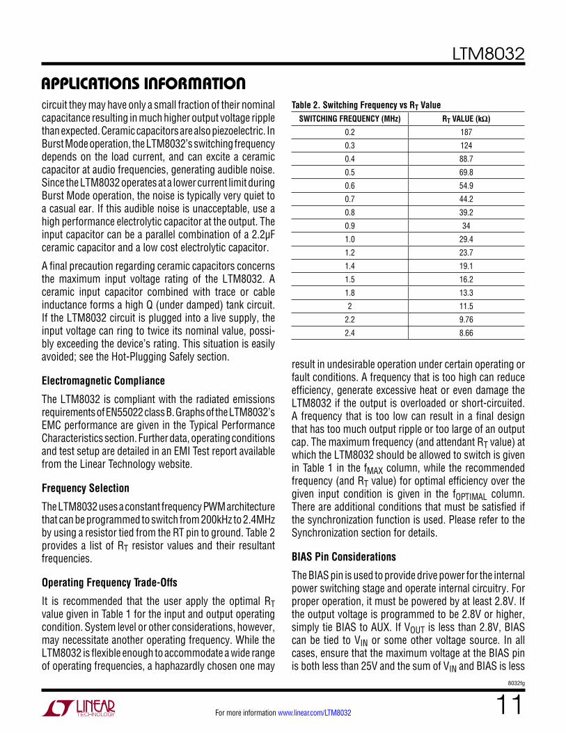
The LTM8032 uses a constant frequency PWM architecture that can be programmed to switch from 200kHz to 2.4MHz by using a resistor tied from the RT pin to ground. Table 2 provides a list of RT resistor values and their resultant frequencies.
Operating Frequency Trade-Offs
It is recommended that the user apply the optimal RT value given in Table 1 for the input and output operating condition. System level or other considerations, however, may necessitate another operating frequency. While the LTM8032 is flexible enough to accommodate a wide range of operating frequencies, a haphazardly chosen one may
result in undesirable operation under certain operating or fault conditions. A frequency that is too high can reduce efficiency, generate excessive heat or even damage the LTM8032 if the output is overloaded or short-circuited. A frequency that is too low can result in a final design that has too much output ripple or too large of an output cap. The maximum frequency (and attendant RT value) at which the LTM8032 should be allowed to switch is given in Table 1 in the fMAX column, while the recommended frequency (and RT value) for optimal efficiency over the given input condition is given in the fOPTIMAL column. There are additional conditions that must be satisfied if the synchronization function is used. Please refer to the Synchronization section for details.
BIAS Pin Considerations
The BIAS pin is used to provide drive power for the internal power switching stage and operate internal circuitry. For proper operation, it must be powered by at least 2.8V. If the output voltage is programmed to be 2.8V or higher, simply tie BIAS to AUX. If VOUT is less than 2.8V, BIAS can be tied to VIN or some other voltage source. In all cases, ensure that the maximum voltage at the BIAS pin is both less than 25V and the sum of VIN and BIAS is less
Table 2. Switching Frequency vs RT ValueSWITCHING FREQUENCY (MHz) RT VALUE (kΩ)
0.2 187
0.3 124
0.4 88.7
0.5 69.8
0.6 54.9
0.7 44.2
0.8 39.2
0.9 34
1.0 29.4
1.2 23.7
1.4 19.1
1.5 16.2
1.8 13.3
2 11.5
2.2 9.76
2.4 8.66
LTM8032
128032fg
For more information www.linear.com/LTM8032
applicaTions inForMaTionthan 56V. If BIAS power is applied from a remote or noisy voltage source, it may be necessary to apply a decoupling capacitor locally to the LTM8032.
Load Sharing
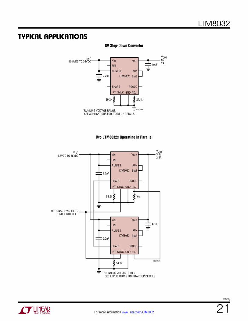
Two or more LTM8032s may be paralleled to produce higher currents. This may, however, alter the EMI performance of the LTM8032s. To do this, tie the VIN, ADJ, VOUT and SHARE pins of all the paralleled LTM8032s together. To ensure that paralleled modules start up together, the RUN/SS pins may be tied together, as well. Synchronize the LTM8032s to an external clock to eliminate beat frequen-cies, if required. If the RUN/SS pins are not tied together, make sure that the same valued soft-start capacitors are used for each module. An example of two LTM8032 modules configured for load sharing is given in the Typical Applications section.
For current sharing applications using multiple LTM8032s, the ADJ pins for all regulators may be combined using one resistor to ground as determined by:
RADJ =
196.71N
VOUT – 0.79
where N is the number of paralleled modules and RADJ is in kΩ.
Burst Mode Operation
To enhance efficiency at light loads, the LTM8032 auto-matically switches to Burst Mode operation which keeps the output capacitor charged to the proper voltage while minimizing the input quiescent current. During Burst Mode operation, the LTM8032 delivers single cycle bursts of current to the output capacitor followed by sleep periods where the output power is delivered to the load by the output capacitor. In addition, VIN and BIAS quiescent currents are reduced to typically 25µA and 60µA respectively during the sleep time. As the load current decreases towards a no-load condition, the percentage of time that the LTM8032 operates in sleep mode increases and the average input current is greatly reduced, resulting in higher efficiency. Burst Mode operation is enabled by tying SYNC to GND. Figure 1. The LTM8032 Needs More Voltage to Start Than Run
To disable Burst Mode operation, tie SYNC to a stable voltage above 0.7V or synchronize to an external clock. Do not leave the SYNC pin floating.
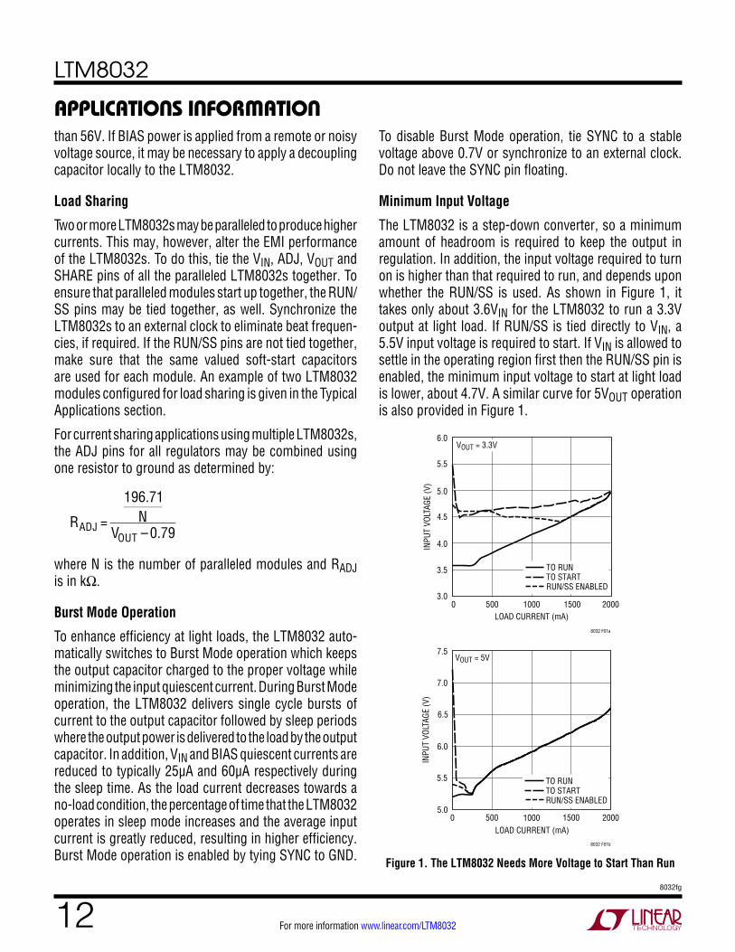
Minimum Input Voltage
The LTM8032 is a step-down converter, so a minimum amount of headroom is required to keep the output in regulation. In addition, the input voltage required to turn on is higher than that required to run, and depends upon whether the RUN/SS is used. As shown in Figure 1, it takes only about 3.6VIN for the LTM8032 to run a 3.3V output at light load. If RUN/SS is tied directly to VIN, a 5.5V input voltage is required to start. If VIN is allowed to settle in the operating region first then the RUN/SS pin is enabled, the minimum input voltage to start at light load is lower, about 4.7V. A similar curve for 5VOUT operation is also provided in Figure 1.
LOAD CURRENT (mA)0
3.0
INPU
T VO
LTAG
E (V
)
3.5
4.0
4.5
5.0
5.5
6.0
500 1000 1500 2000
8032 F01a
TO RUNTO STARTRUN/SS ENABLED
VOUT = 3.3V
LOAD CURRENT (mA)0
INPU
T VO
LTAG
E (V
)
6.5
7.0
7.5
8032 F01b
6.0
5.5
5.0500 1000 1500 2000
TO RUNTO STARTRUN/SS ENABLED
VOUT = 5V
LTM8032
138032fg
For more information www.linear.com/LTM8032
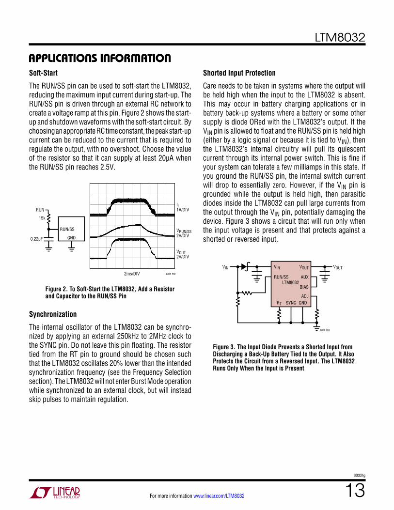
Soft-Start
The RUN/SS pin can be used to soft-start the LTM8032, reducing the maximum input current during start-up. The RUN/SS pin is driven through an external RC network to create a voltage ramp at this pin. Figure 2 shows the start-up and shutdown waveforms with the soft-start circuit. By choosing an appropriate RC time constant, the peak start-up current can be reduced to the current that is required to regulate the output, with no overshoot. Choose the value of the resistor so that it can supply at least 20µA when the RUN/SS pin reaches 2.5V.
applicaTions inForMaTion
Figure 2. To Soft-Start the LTM8032, Add a Resistor and Capacitor to the RUN/SS Pin
Shorted Input Protection
Care needs to be taken in systems where the output will be held high when the input to the LTM8032 is absent. This may occur in battery charging applications or in battery back-up systems where a battery or some other supply is diode ORed with the LTM8032’s output. If the VIN pin is allowed to float and the RUN/SS pin is held high (either by a logic signal or because it is tied to VIN), then the LTM8032’s internal circuitry will pull its quiescent current through its internal power switch. This is fine if your system can tolerate a few milliamps in this state. If you ground the RUN/SS pin, the internal switch current will drop to essentially zero. However, if the VIN pin is grounded while the output is held high, then parasitic diodes inside the LTM8032 can pull large currents from the output through the VIN pin, potentially damaging the device. Figure 3 shows a circuit that will run only when the input voltage is present and that protects against a shorted or reversed input.
Figure 3. The Input Diode Prevents a Shorted Input from Discharging a Back-Up Battery Tied to the Output. It Also Protects the Circuit from a Reversed Input. The LTM8032 Runs Only When the Input is Present
VOUTVIN
RUN/SS
BIAS
RT
ADJ
LTM8032
8032 F03
VOUT
GND
VIN
AUX
SYNC
Synchronization
The internal oscillator of the LTM8032 can be synchro-nized by applying an external 250kHz to 2MHz clock to the SYNC pin. Do not leave this pin floating. The resistor tied from the RT pin to ground should be chosen such that the LTM8032 oscillates 20% lower than the intended synchronization frequency (see the Frequency Selection section). The LTM8032 will not enter Burst Mode operation while synchronized to an external clock, but will instead skip pulses to maintain regulation.
8023 F02
IL1A/DIV
VRUN/SS2V/DIV
VOUT2V/DIV
RUN/SS
GND0.22µF
RUN
15k
2ms/DIV
LTM8032
148032fg
For more information www.linear.com/LTM8032
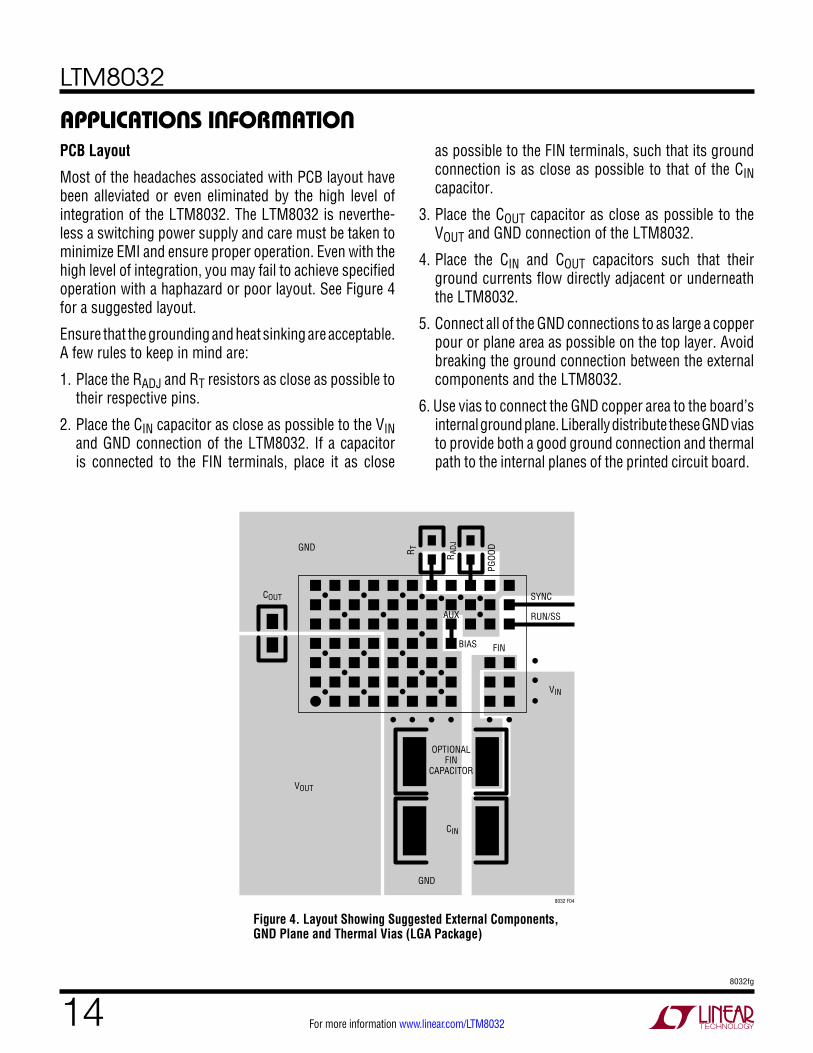
applicaTions inForMaTionPCB Layout
Most of the headaches associated with PCB layout have been alleviated or even eliminated by the high level of integration of the LTM8032. The LTM8032 is neverthe-less a switching power supply and care must be taken to minimize EMI and ensure proper operation. Even with the high level of integration, you may fail to achieve specified operation with a haphazard or poor layout. See Figure 4 for a suggested layout.
Ensure that the grounding and heat sinking are acceptable. A few rules to keep in mind are:
1. Place the RADJ and RT resistors as close as possible to their respective pins.
2. Place the CIN capacitor as close as possible to the VIN and GND connection of the LTM8032. If a capacitor is connected to the FIN terminals, place it as close
GND
COUT
CIN
8032 F04
VIN
FIN
RUN/SS
SYNC
PGOO
D
R ADJR T
AUX
BIAS
VOUT
GND
OPTIONALFIN
CAPACITOR
Figure 4. Layout Showing Suggested External Components, GND Plane and Thermal Vias (LGA Package)
as possible to the FIN terminals, such that its ground connection is as close as possible to that of the CIN capacitor.
3. Place the COUT capacitor as close as possible to the VOUT and GND connection of the LTM8032.
4. Place the CIN and COUT capacitors such that their ground currents flow directly adjacent or underneath the LTM8032.
5. Connect all of the GND connections to as large a copper pour or plane area as possible on the top layer. Avoid breaking the ground connection between the external components and the LTM8032.
6. Use vias to connect the GND copper area to the board’s internal ground plane. Liberally distribute these GND vias to provide both a good ground connection and thermal path to the internal planes of the printed circuit board.
LTM8032
158032fg
For more information www.linear.com/LTM8032
Hot-Plugging Safely
The small size, robustness and low impedance of ceramic capacitors make them an attractive option for the input bypass capacitor of LTM8032. However, these capacitors can cause problems if the LTM8032 is plugged into a live or fast rising or falling supply (see Linear Technology Application Note 88 for a complete discussion). The low loss ceramic capacitor combined with stray inductance in series with the power source forms an under-damped tank circuit, and the voltage at the VIN pin of the LTM8032 can ring to twice the nominal input voltage, possibly exceeding the LTM8032’s rating and damaging the part. A similar phenomenon can occur inside the LTM8032 module, at the output of the integrated EMI filter, with the same potential of damaging the part.
If the input supply is poorly controlled or the user will be plugging the LTM8032 into an energized supply, the input network should be designed to prevent this overshoot. Fig-ure 5 shows the waveforms that result when an LTM8032 circuit is connected to a 24V supply through six feet of 24-gauge twisted pair. The first plot (5a) is the response
applicaTions inForMaTionwith a 2.2µF ceramic capacitor at the input. The input voltage rings as high as 35V and the input current peaks at 20A. One method of damping the tank circuit is to add another capacitor with a series resistor to the circuit. An alternative solution is shown in Figure 5b. A 0.7Ω resistor is added in series with the input to eliminate the voltage overshoot (it also reduces the peak input current). A 0.1µF capacitor improves high frequency filtering. For high input voltages its impact on efficiency is minor, reducing ef-ficiency less than one-half percent for a 5V output at full load operating from 24V. By far the most popular method of controlling overshoot is shown in Figure 5c, where an aluminum electrolytic capacitor has been connected to FIN. This capacitor’s high equivalent series resistance damps the circuit and eliminates the voltage overshoot. The extra capacitor improves low frequency ripple filtering and can slightly improve the efficiency of the circuit, though it is likely to be the largest component in the circuit. Figure 5c shows the capacitor added to the VIN terminals, but placing the electrolytic capacitor at the FIN terminals can improve the LTM8032’s EMI filtering as well as guard against overshoots caused by the Q of the integrated filter.

LTM8032
168032fg
For more information www.linear.com/LTM8032
applicaTions inForMaTion
Figure 5. A Well Chosen Input Network Prevents Input Voltage Overshoot and Ensures Reliable Operation When the LTM8032 is Hot-Plugged to a Live Supply
+
LTM8032
4.7µF
VIN20V/DIV
IIN10A/DIV
20µs/DIV
VIN
CLOSING SWITCHSIMULATES HOT PLUG
IIN
(5a)
(5b)
LOWIMPEDANCEENERGIZED24V SUPPLY
STRAYINDUCTANCEDUE TO 6 FEET(2 METERS) OFTWISTED PAIR
+
LTM8032
4.7µF0.1µF
0.7Ω VIN20V/DIV
IIN10A/DIV
20µs/DIV
DANGER
RINGING VIN MAY EXCEEDABSOLUTE MAXIMUM RATING
(5c)
+4.7µF
22µF35V
AI.EI.
8032 F05
VIN20V/DIV
IIN10A/DIV
20µs/DIV
+
VIN
LTM8032VIN
FIN

LTM8032
178032fg
For more information www.linear.com/LTM8032
Thermal Considerations
The LTM8032 output current may need to be derated if it is required to operate in a high ambient temperature or deliver a large amount of continuous power. The amount of current derating is dependent upon the input voltage, output power and ambient temperature. The temperature rise curves given in the Typical Performance Character-istics section can be used as a guide. These curves were generated by an LTM8032 mounted to a 36cm2 4-layer FR4 printed circuit board. Boards of other sizes and layer count can exhibit different thermal behavior, so it is incumbent upon the user to verify proper operation over the intended system’s line, load and environmental operating conditions.
The thermal resistance numbers listed in the Pin Con-figuration are based on modeling the µModule package mounted on a test board specified per JESD51-9 “Test Boards for Area Array Surface Mount Package Thermal Measurements.” The thermal coefficients provided in this page are based on JESD 51-12 “Guidelines for Reporting and Using Electronic Package Thermal Information.”
For increased accuracy and fidelity to the actual application, many designers use FEA to predict thermal performance. To that end, the Pin Configuration typically gives four thermal coefficients:
• θJA – Thermal resistance from junction to ambient.
• θJCbottom – Thermal resistance from junction to the bottom of the product case.
• θJCtop – Thermal resistance from junction to top of the product case.
• θJB – Thermal resistance from junction to the printed circuit board.
While the meaning of each of these coefficients may seem to be intuitive, JEDEC has defined each to avoid confu-sion and inconsistency. These definitions are given in JESD 51-12, and are quoted or paraphrased in the following:
• θJA is the natural convection junction-to-ambient air thermal resistance measured in a one cubic foot sealed enclosure. This environment is sometimes referred to as “still air” although natural convection causes the air to move. This value is determined with the part mounted to a JESD 51-9 defined test board, which does not reflect an actual application or viable operating condition.
• θJCbottom is the junction-to-board thermal resistance with all of the component power dissipation flowing through the bottom of the package. In the typical µModule regulator, the bulk of the heat flows out the bottom of the package, but there is always heat flow out into the ambient environment. As a result, this thermal resistance value may be useful for comparing packages but the test conditions don’t generally match the user’s application.
• θJCtop is determined with nearly all of the component power dissipation flowing through the top of the pack-age. As the electrical connections of the typical µModule regulator are on the bottom of the package, it is rare for an application to operate such that most of the heat flows from the junction to the top of the part. As in the case of θJCbottom, this value may be useful for comparing packages but the test conditions don’t generally match the user’s application.
• θJB is the junction-to-board thermal resistance where almost all of the heat flows through the bottom of the µModule regulator and into the board, and is really the sum of the θJCbottom and the thermal resistance of the bottom of the part through the solder joints and through a portion of the board. The board temperature is mea-sured a specified distance from the package, using a two sided, two layer board. This board is described in JESD 51-9.
applicaTions inForMaTion
LTM8032
188032fg
For more information www.linear.com/LTM8032
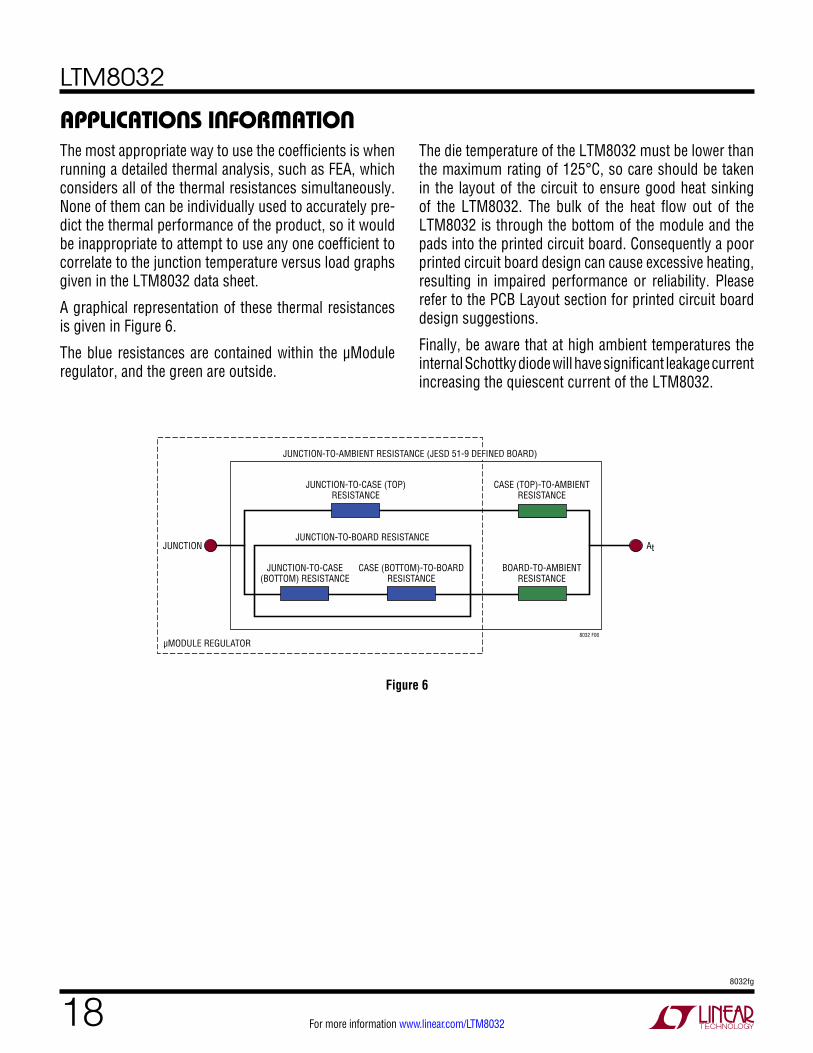
The most appropriate way to use the coefficients is when running a detailed thermal analysis, such as FEA, which considers all of the thermal resistances simultaneously. None of them can be individually used to accurately pre-dict the thermal performance of the product, so it would be inappropriate to attempt to use any one coefficient to correlate to the junction temperature versus load graphs given in the LTM8032 data sheet.
A graphical representation of these thermal resistances is given in Figure 6.
The blue resistances are contained within the µModule regulator, and the green are outside.
The die temperature of the LTM8032 must be lower than the maximum rating of 125°C, so care should be taken in the layout of the circuit to ensure good heat sinking of the LTM8032. The bulk of the heat flow out of the LTM8032 is through the bottom of the module and the pads into the printed circuit board. Consequently a poor printed circuit board design can cause excessive heating, resulting in impaired performance or reliability. Please refer to the PCB Layout section for printed circuit board design suggestions.
Finally, be aware that at high ambient temperatures the internal Schottky diode will have significant leakage current increasing the quiescent current of the LTM8032.
applicaTions inForMaTion
8032 F06
µMODULE REGULATOR
JUNCTION-TO-CASE (TOP)RESISTANCE
JUNCTION-TO-BOARD RESISTANCE
JUNCTION-TO-AMBIENT RESISTANCE (JESD 51-9 DEFINED BOARD)
CASE (TOP)-TO-AMBIENTRESISTANCE
BOARD-TO-AMBIENTRESISTANCE
JUNCTION-TO-CASE(BOTTOM) RESISTANCE
JUNCTION At
CASE (BOTTOM)-TO-BOARDRESISTANCE
Figure 6
LTM8032
198032fg
For more information www.linear.com/LTM8032
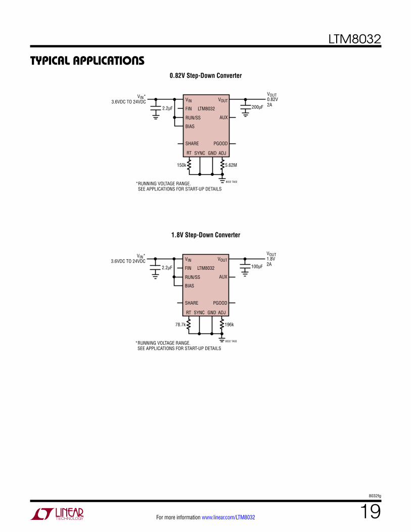
Typical applicaTions0.82V Step-Down Converter
1.8V Step-Down Converter
RT
SHARE
5.62M
*RUNNING VOLTAGE RANGE. SEE APPLICATIONS FOR START-UP DETAILS
150k
VIN
FIN2.2µF 200µF
VOUT0.82V2A
RUN/SS
VIN*3.6VDC TO 24VDC
PGOOD
BIAS
LTM8032
AUX
VOUT
SYNC GND
8032 TA02
ADJ
RT
SHARE
196k
*RUNNING VOLTAGE RANGE. SEE APPLICATIONS FOR START-UP DETAILS
78.7k
VIN
FIN2.2µF 100µF
VOUT1.8V2A
RUN/SS
VIN*3.6VDC TO 24VDC
PGOOD
BIAS
LTM8032
AUX
VOUT
SYNC GND
8032 TA03
ADJ
LTM8032
208032fg
For more information www.linear.com/LTM8032
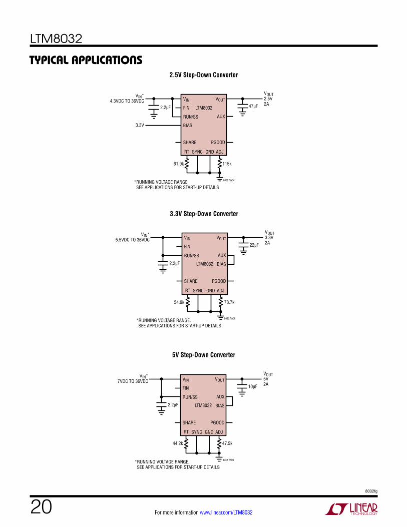
Typical applicaTions2.5V Step-Down Converter
5V Step-Down Converter
3.3V Step-Down Converter
RT
SHARE
115k
*RUNNING VOLTAGE RANGE. SEE APPLICATIONS FOR START-UP DETAILS
61.9k
VIN
FIN2.2µF 47µF
VOUT2.5V2A
RUN/SS
VIN*4.3VDC TO 36VDC
3.3V
PGOOD
BIAS
LTM8032
AUX
VOUT
SYNC GND
8032 TA04
ADJ
RT
SHARE
VIN
FIN
2.2µF
22µF
78.7k54.9k
VOUT3.3V2A
RUN/SS
VIN*5.5VDC TO 36VDC
PGOOD
BIASLTM8032
AUX
VOUT
SYNC GND
8032 TA08
ADJ
*RUNNING VOLTAGE RANGE. SEE APPLICATIONS FOR START-UP DETAILS
RT
SHARE
VIN
FIN
2.2µF
10µF
47.5k44.2k
VOUT5V2A
RUN/SS
VIN*7VDC TO 36VDC
PGOOD
BIASLTM8032
AUX
VOUT
SYNC GND
8032 TA05
ADJ
*RUNNING VOLTAGE RANGE. SEE APPLICATIONS FOR START-UP DETAILS
LTM8032
218032fg
For more information www.linear.com/LTM8032
Typical applicaTions8V Step-Down Converter
Two LTM8032s Operating in Parallel
RT
SHARE
VIN
FIN
2.2µF
10µF
27.4k39.2k
VOUT8V2A
RUN/SS
VIN*10.5VDC TO 36VDC
PGOOD
BIASLTM8032
AUX
VOUT
SYNC GND
8032 TA06
ADJ
*RUNNING VOLTAGE RANGE. SEE APPLICATIONS FOR START-UP DETAILS
RT
SHARE
VIN
FIN
2.2µF
40k54.9k
8032 TA07
47µF
VOUT3.3V3.5A
RUN/SS
VIN*5.5VDC TO 36VDC
OPTIONAL SYNC TIE TOGND IF NOT USED
PGOOD
BIASLTM8032
AUX
VOUT
SYNC GND ADJ
RT
SHARE
54.9k
VIN
FIN
2.2µF
RUN/SS
PGOOD
BIASLTM8032
AUX
VOUT
SYNC GND ADJ
*RUNNING VOLTAGE RANGE. SEE APPLICATIONS FOR START-UP DETAILS
LTM8032
228032fg
For more information www.linear.com/LTM8032
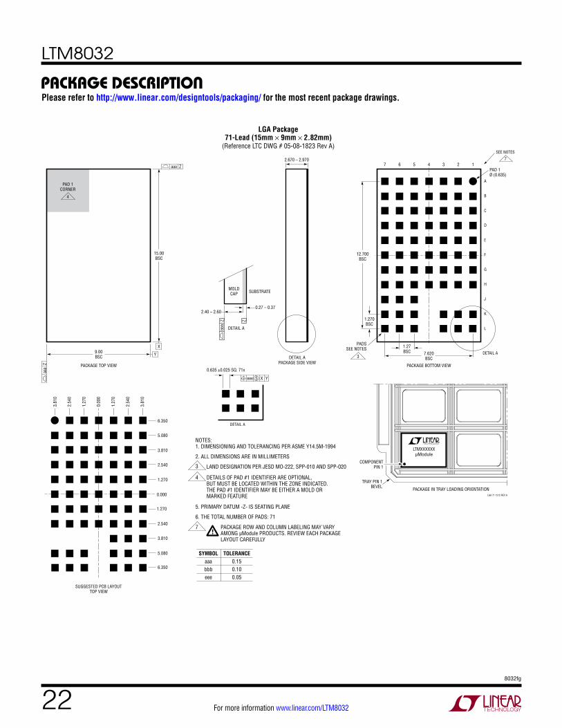
package DescripTionPlease refer to http://www.linear.com/designtools/packaging/ for the most recent package drawings.
9.00BSC
PACKAGE TOP VIEW
LGA 71 1212 REV A
15.00BSC
4
PAD 1CORNER
3
PADSSEE NOTESX
Y
aaa Z
aaa
Z
2.670 – 2.970
DETAIL APACKAGE SIDE VIEW
DETAIL A
SUBSTRATEMOLDCAP
0.27 – 0.372.40 – 2.60
bbb
Z Z 1.270BSC
0.635 ±0.025 SQ. 71x
12.700BSC
7.620BSC
PAD 1Ø (0.635)
PACKAGE IN TRAY LOADING ORIENTATION
2.540
2.540
1.270
5.080
5.080
6.350
6.350
3.810
3.810
0.000
1.270
3.81
0
3.81
0
2.54
0
2.54
0
1.27
0
1.27
0
0.00
0
SUGGESTED PCB LAYOUTTOP VIEW
LTMXXXXXXµModule
TRAY PIN 1BEVEL
COMPONENTPIN 1
PACKAGE BOTTOM VIEW
67 5 1234
L
K
J
H
G
F
E
D
C
B
A
NOTES:1. DIMENSIONING AND TOLERANCING PER ASME Y14.5M-1994
2. ALL DIMENSIONS ARE IN MILLIMETERS
LAND DESIGNATION PER JESD MO-222, SPP-010 AND SPP-020
5. PRIMARY DATUM -Z- IS SEATING PLANE
6. THE TOTAL NUMBER OF PADS: 71
4
3
DETAILS OF PAD #1 IDENTIFIER ARE OPTIONAL,BUT MUST BE LOCATED WITHIN THE ZONE INDICATED.THE PAD #1 IDENTIFIER MAY BE EITHER A MOLD OR MARKED FEATURE
DETAIL A
S YXeee
DETAIL A
SYMBOLaaabbbeee
TOLERANCE0.150.100.05
1.27BSC
LGA Package71-Lead (15mm × 9mm × 2.82mm)
(Reference LTC DWG # 05-08-1823 Rev A)
7 PACKAGE ROW AND COLUMN LABELING MAY VARY AMONG µModule PRODUCTS. REVIEW EACH PACKAGE LAYOUT CAREFULLY
!
7
SEE NOTES
LTM8032
238032fg
For more information www.linear.com/LTM8032
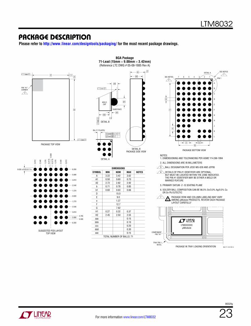
package DescripTionPlease refer to http://www.linear.com/designtools/packaging/ for the most recent package drawings.
PACKAGE TOP VIEW
4
PIN “A1”CORNER
YX
aaa Z
aaa Z
DETAIL A
PACKAGE BOTTOM VIEW
3
SEE NOTES
L
K
J
H
G
F
E
D
C
B
A
1234567PIN 1
BGA 71 1212 REV A
TRAY PIN 1BEVEL
PACKAGE IN TRAY LOADING ORIENTATION
COMPONENTPIN “A1”
NOTES:1. DIMENSIONING AND TOLERANCING PER ASME Y14.5M-1994
2. ALL DIMENSIONS ARE IN MILLIMETERS
BALL DESIGNATION PER JESD MS-028 AND JEP95
4
3
DETAILS OF PIN #1 IDENTIFIER ARE OPTIONAL,BUT MUST BE LOCATED WITHIN THE ZONE INDICATED.THE PIN #1 IDENTIFIER MAY BE EITHER A MOLD OR MARKED FEATURE
DETAIL A
Øb (71 PLACES)
DETAIL B
SUBSTRATE
A
A1
b1
ccc Z
DETAIL BPACKAGE SIDE VIEW
MOLDCAP
Z
M X YZdddM Zeee
SYMBOLA
A1A2b
b1DEeFG
H1H2aaabbbcccdddeee
MIN3.220.502.720.710.60
0.272.45
NOM3.420.602.820.780.6315.09.0
1.2712.77.620.322.50
MAX3.620.702.920.850.66
0.372.550.150.100.200.300.15
NOTES
DIMENSIONS
TOTAL NUMBER OF BALLS: 71
A2
D
E
e
e
b
F
G
SUGGESTED PCB LAYOUTTOP VIEW
0.000
1.270
6.350
2.540
3.810
5.080
6.350
1.270
2.540
3.810
5.080
3.81
0
2.54
0
1.27
0
3.81
0
2.54
0
1.27
0
0.31
75
0.31
750.
000
4.765
5.395
LTMXXXXXXµModule
// b
bb Z Z
H2H1
b
5. PRIMARY DATUM -Z- IS SEATING PLANE
6. SOLDER BALL COMPOSITION CAN BE 96.5% Sn/3.0% Ag/0.5% Cu OR Sn Pb EUTECTIC
0.630 ±0.025 Ø 71x
BGA Package71-Lead (15mm × 9.00mm × 3.42mm)(Reference LTC DWG # 05-08-1885 Rev A)
7 PACKAGE ROW AND COLUMN LABELING MAY VARY AMONG µModule PRODUCTS. REVIEW EACH PACKAGE LAYOUT CAREFULLY
!
7
SEE NOTES

LTM8032
248032fg
For more information www.linear.com/LTM8032
package DescripTion
PINSIGNAL
DESCRIPTION
A1 VOUT
A2 VOUT
A3 VOUT
A4 VOUT
A5 GND
A6 GND
A7 GND
B1 VOUT
B2 VOUT
B3 VOUT
B4 VOUT
B5 GND
B6 GND
B7 GND
C1 VOUT
C2 VOUT
C3 VOUT
C4 VOUT
C5 GND
C6 GND
C7 GND
D1 VOUT
D2 VOUT
D3 VOUT
D4 VOUT
D5 GND
D6 GND
D7 GND
E1 GND
E2 GND
E3 GND
E4 GND
E5 GND
E6 GND
PINSIGNAL
DESCRIPTION
E7 GND
F1 GND
F2 GND
F3 GND
F4 GND
F5 GND
F6 GND
F7 GND
G1 GND
G2 GND
G3 GND
G4 GND
G5 GND
G6 GND
G7 RT
H1 GND
H2 GND
H3 GND
H4 BIAS
H5 AUX
H6 GND
H7 SHARE
J5 GND
J6 GND
J7 ADJ
K1 VIN
K2 VIN
K3 FIN
K5 GND
K6 GND
K7 PGOOD
L1 VIN
L2 VIN
L3 FIN
L5 RUN/SS
L6 SYNC
L7 GND
Table 3. LTM8032 Pinout (Sorted by Pin Number)
LTM8032
258032fg
For more information www.linear.com/LTM8032
Information furnished by Linear Technology Corporation is believed to be accurate and reliable. However, no responsibility is assumed for its use. Linear Technology Corporation makes no representa-tion that the interconnection of its circuits as described herein will not infringe on existing patent rights.
revision hisToryREV DATE DESCRIPTION PAGE NUMBER
D 8/11 Added BGA package. Changes reflected throughout the data sheet. 1 to 26
E 9/11 Updated BGA Pin Configuration diagram. 2
F 2/12 Indicate Figure 4 is Layout Example for LGA PackageConsolidate BGA and LGA Pinout Table
1424
G 1/14 Added SnPb terminal finish product option 1, 2
(Revision history begins at Rev D)
LTM8032
268032fg
For more information www.linear.com/LTM8032(408) 432-1900 ● FAX: (408) 434-0507 ● www.linear.com/LTM8032
Linear Technology Corporation1630 McCarthy Blvd., Milpitas, CA 95035-7417
LINEAR TECHNOLOGY CORPORATION 2009
LT 0114 REV G • PRINTED IN USA
relaTeD parTs
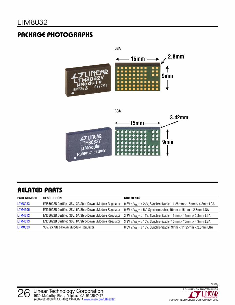
package phoTographs
PART NUMBER DESCRIPTION COMMENTS
LTM8033 EN55022B Certified 36V, 3A Step-Down µModule Regulator 0.8V ≤ VOUT ≤ 24V, Synchronizable, 11.25mm × 15mm × 4.3mm LGA
LTM4606 EN55022B Certified 28V, 6A Step-Down µModule Regulator 0.6V ≤ VOUT ≤ 5V, Synchronizable, 15mm × 15mm × 2.8mm LGA
LTM4612 EN55022B Certified 36V, 5A Step-Down µModule Regulator 3.3V ≤ VOUT ≤ 15V, Synchronizable, 15mm × 15mm × 2.8mm LGA
LTM4613 EN55022B Certified 36V, 8A Step-Down µModule Regulator 3.3V ≤ VOUT ≤ 15V, Synchronizable, 15mm × 15mm × 4.3mm LGA
LTM8023 36V, 2A Step-Down µModule Regulator 0.8V ≤ VOUT ≤ 10V, Synchronizable, 9mm × 11.25mm × 2.8mm LGA
LGA
BGA