ltm4605 - high efficiency buck-boost dc/dc µmodule …€¦ · ltm4605 1 4605fd for more...
TRANSCRIPT

LTM4605
14605fd
For more information www.linear.com/LTM4605
Features Description
High Efficiency Buck-Boost DC/DC µModule Regulator
The LTM®4605 is a high efficiency switching mode buck-boost power supply. Included in the package are the switching controller, power FETs, and support components. Operating over an input voltage range of 4.5V to 20V, the LTM4605 supports an output voltage range of 0.8V to 16V, set by a resistor. This high efficiency design delivers up to 5A continuous current in boost mode (12A in buck mode). Only the inductor, sense resistor, bulk input and output capacitors are needed to finish the design.
The low profile package enables utilization of unused space on the bottom of PC boards for high density point of load regulation. The high switching frequency and current mode architecture enable a very fast transient response to line and load changes. The LTM4605 can be frequency synchronized with an external clock to reduce undesirable frequency harmonics.
Fault protection features include overvoltage and foldback current protection. The DC/DC µModule® regulator is of-fered in a small and thermally enhanced 15mm × 15mm × 2.8mm LGA package. The LTM4605 is Pb-free and RoHS compliant.
applications
n Single Inductor Architecture Allows VIN Above, Below or Equal to VOUT
n Wide VIN Range: 4.5V to 20Vn Wide VOUT Range: 0.8V to 16Vn 5A DC Typical (12A DC Typical at Buck Mode)n High Efficiency Up to 98%n Current Mode Controln Power Good Output Signaln Phase-Lockable Fixed Frequency: 200kHz to 400kHzn Ultrafast Transient Responsen Current Foldback Protectionn Output Overvoltage Protectionn Small, Low Profile Surface Mount LGA Package
(15mm × 15mm × 2.8mm)
n Telecom, Servers and Networking Equipmentn Industrial and Automotive Equipmentn High Power Battery-Operated DevicesL, LT, LTC, LTM, Linear Technology, the Linear logo, µModule ad PolyPhase are registered trademarks and No RSENSE is a trademark of Linear Technology Corporation. All other trademarks are the property of their respective owners.
VIN (V)5 6 7 8 9 10 11 12 13 14 15 16 17 18 19
EFFI
CIEN
CY (%
)
99
98
97
96
95
94
93
92
91
90
POWER LOSS (W
)
8
0
7
6
5
4
3
2
1
4605 TA01b
20
VOUT = 12VILOAD = 5Af = 200kHz
typical application12V/5A Buck-Boost DC/DC µModule Regulator with 4.5V to 20V Input Efficiency and Power Loss
vs Input Voltage
VOUT
FCB
RUN
SW1
SW2
RSENSE
SENSE–SS
VFBSGND
PLLIN
LTM4605 4.7µH
7.15k
10µF35V
330µF25V
4605 TA01
VOUT12V5A
CLOCK SYNC
VIN
PGND
VIN4.5V TO 20V
0.1µF
10µF35V
+
ON/OFF
SENSE+
6mΩ

LTM4605
24605fd
For more information www.linear.com/LTM4605
absolute MaxiMuM ratings
VIN ............................................................. –0.3V to 20VVOUT ..............................................................0.8V to 16VINTVCC, EXTVCC, RUN, SS, PGOOD ............. –0.3V to 7VSW1, SW2 (Note 6) ....................................... –5V to 20VVFB, COMP ................................................ –0.3V to 2.4VFCB, STBYMD .......................................–0.3V to INTVCCPLLIN ........................................................ –0.3V to 5.5VPLLFLTR ................................................... –0.3V to 2.7VOperating Temperature Range
(Note 2) ...............................................–40°C to 85°CStorage Temperature Range .................. –55°C to 125°C
(Note 1)pin conFiguration(See Table 6. Pin Assignment)
LGA PACKAGE141-LEAD (15mm × 15mm × 2.8mm)
BANK 2
BANK 1
BANK 3
BANK 4
BANK 5
BANK 6
TOP VIEW
1 2 3 4 5 6 7 8 109 11 12
L
K
J
H
G
F
E
D
C
B
M
A
TJMAX = 125°C, θJP = 4°C/W
WEIGHT = 1.5g
electrical characteristics The l denotes the specifications which apply over the full operating temperature range, otherwise specifications are at TA = 25°C (Note 2), VIN = 12V. Per typical application (front page) configuration.
SYMBOL PARAMETER CONDITIONS MIN TYP MAX UNITS
Input Specifications
VIN(DC) Input DC Voltage l 4.5 20 V
VIN(UVLO) Undervoltage Lockout Threshold VIN Falling l 3.4 4 V
IQ(VIN) Input Supply Bias Current Normal Standby Shutdown Supply Current
VRUN = 0V, VSTBYMD > 2V VRUN = 0V, VSTBYMD = Open
2.8 1.6 35
60
mA mA µA
orDer inForMation
PART NUMBER PAD OR BALL FINISH
PART MARKING* PACKAGE TYPE
MSL RATING
TEMPERATURE RANGE (SEE NOTE 2)DEVICE FINISH CODE
LTM4605EV#PBF Au (RoHS) LTM4605V e4 LGA 3 –40°C to 85°C
LTM4605IV#PBF Au (RoHS) LTM4605V e4 LGA 3 –40°C to 85°C
Consult Marketing for parts specified with wider operating temperature ranges. *Device temperature grade is indicated by a label on the shipping container. Pad or ball finish code is per IPC/JEDEC J-STD-609.•Terminal Finish Part Marking:
www.linear.com/leadfree
•Recommended LGA and BGA PCB Assembly and Manufacturing Procedures: www.linear.com/umodule/pcbassembly
•LGA and BGA Package and Tray Drawings: www.linear.com/packaging

LTM4605
34605fd
For more information www.linear.com/LTM4605
electrical characteristics The l denotes the specifications which apply over the full operating temperature range, otherwise specifications are at TA = 25°C (Note 2), VIN = 12V. Per typical application (front page) configuration.
SYMBOL PARAMETER CONDITIONS MIN TYP MAX UNITS
Output Specifications
IOUTDC Output Continuous Current Range (See Output Current Derating Curves for Different VIN, VOUT and TA)
VIN = 12V, VOUT = 5V VIN = 6V, VOUT = 12V
12 5
A A
ΔVFB/VFB(NOM) Reference Voltage Line Regulation Accuracy
VIN = 4.5V to 20V, VCOMP = 1.2V (Note 3) 0.002 0.02 %/V
ΔVFB/VFB(LOAD) Load Regulation Accuracy VCOMP = 1.2V to 0.7V VCOMP = 1.2V to 1.8V (Note 3)
l
l
0.15 –0.15
0.5 –0.5
% %
Switch Section
M1 tr Turn-On Time (Note 4) Drain to Source Voltage VDS = 12V, Bias Current ISW = 10mA
50 ns
M1 tf Turn-Off Time Drain to Source Voltage VDS = 12V, Bias Current ISW = 10mA
40 ns
M3 tr Turn-On Time Drain to Source Voltage VDS = 12V, Bias Current ISW = 10mA
25 ns
M3 tf Turn-Off Time Drain to Source Voltage VDS = 12V, Bias Current ISW = 10mA
20 ns
M2, M4 tr Turn-On Time Drain to Source Voltage VDS = 12V, Bias Current ISW = 10mA
20 ns
M2, M4 tf Turn-Off Time Drain to Source Voltage VDS = 12V, Bias Current ISW = 10mA
20 ns
t1d M1 Off to M2 On Delay (Note 4) Drain to Source Voltage VDS = 12V, Bias Current ISW = 10mA
50 ns
t2d M2 Off to M1 On Delay Drain to Source Voltage VDS = 12V, Bias Current ISW = 10mA
50 ns
t3d M3 Off to M4 On Delay Drain to Source Voltage VDS = 12V, Bias Current ISW = 10mA
50 ns
t4d M4 Off to M3 On Delay Drain to Source Voltage VDS = 12V, Bias Current ISW = 10mA
50 ns
Mode Transition 1 M2 Off to M4 On Delay Drain to Source Voltage VDS = 12V, Bias Current ISW = 10mA
220 ns
Mode Transition 2 M4 Off to M2 On Delay Drain to Source Voltage VDS = 12V, Bias Current ISW = 10mA
220 ns
M1 RDS(ON) Static Drain-to-Source On-Resistance Bias Current ISW = 3A 6.5 mΩ
M2 RDS(ON) Static Drain-to-Source On-Resistance Bias Current ISW = 3A 8 12 mΩ
M3 RDS(ON) Static Drain-to-Source On-Resistance Bias Current ISW = 3A 8 12 mΩ
M4 RDS(ON) Static Drain-to-Source On-Resistance Bias Current ISW = 3A 8 12 mΩ
Oscillator and Phase-Locked Loop
fNOM Nominal Frequency VPLLFLTR = 1.2V 260 300 330 kHz
fLOW Lowest Frequency VPLLFLTR = 0V 170 200 220 kHz
fHIGH Highest Frequency VPLLFLTR = 2.4V 340 400 440 kHz
RPLLIN PLLIN Input Resistance 50 kΩ
IPLLFLTR Phase Detector Output Current fPLLIN < fOSC fPLLIN > fOSC
–15 15
µA µA

LTM4605
44605fd
For more information www.linear.com/LTM4605
electrical characteristics The l denotes the specifications which apply over the full operating temperature range, otherwise specifications are at TA = 25°C (Note 2), VIN = 12V. Per typical application (front page) configuration.
SYMBOL PARAMETER CONDITIONS MIN TYP MAX UNITS
Control Section
VFB Feedback Reference Voltage VCOMP = 1.2V l 0.792 0.8 0.808 V
VRUN RUN Pin ON/OFF Threshold 1 1.6 2.2 V
ISS Soft-Start Charging Current VRUN = 2.2V 1 1.7 µA
VSTBYMD(START) Start-Up Threshold VSTBYMD Rising 0.4 0.7 V
VSTBYMD(KA) Keep-Active Power On Threshold VSTBYMD Rising, VRUN = 0V 1.25 V
VFCB Forced Continuous Threshold 0.76 0.8 0.84 V
IFCB Forced Continuous Pin Current VFCB = 0.85V –0.3 –0.2 –0.1 µA
VBURST Burst Inhibit (Constant Frequency) Threshold
Measured at FCB Pin 5.3 5.5 V
DF(BOOST, MAX) Maximum Duty Factor % Switch M4 On 99 %
DF(BUCK, MAX) Maximum Duty Factor % Switch M1 On 99 %
tON(MIN, BUCK) Minimum On-Time for Synchronous Switch in Buck Operation
Switch M1 (Note 5) 200 250 ns
RFBHI Resistor Between VOUT and VFB Pins 99.5 100 100.5 kΩ
Internal VCC Regulator
INTVCC Internal VCC Voltage VIN > 7V, VEXTVCC = 5V l 5.7 6 6.3 V
ΔVLDO/VLDO Internal VCC Load Regulation ICC = 0mA to 20mA, VEXTVCC = 5V 0.3 2 %
VEXTVCC EXTVCC Switchover Voltage ICC = 20mA, VEXTVCC Rising l 5.4 5.6 V
ΔVEXTVCC(HYS) EXTVCC Switchover Hysteresis 300 mV
ΔVEXTVCC EXTVCC Switch Drop Voltage ICC = 20mA, VEXTVCC = 6V 60 150 mV
Current Sensing Section
VSENSE(MAX) Maximum Current Sense Threshold Boost Mode Buck Mode
l
l
–95
160 –130
190 –150
mV mV
VSENSE(MIN, BUCK) Minimum Current Sense Threshold Discontinuous Mode –6 mV
ISENSE Sense Pins Total Source Current VSENSE– = VSENSE
+ = 0V –380 µA
PGOOD
ΔVFBH PGOOD Upper Threshold VFB Rising 5.5 7.5 10 %
ΔVFBL PGOOD Lower Threshold VFB Falling –5.5 –7.5 –10 %
ΔVFB(HYS) PGOOD Hysteresis VFB Returning 2.5 %
VPGL PGOOD Low Voltage IPGOOD = 2mA 0.2 0.3 V
IPGOOD PGOOD Leakage Current VPGOOD = 5V 1 µA
Note 1: Stresses beyond those listed under Absolute Maximum Ratings may cause permanent damage to the device. Exposure to any Absolute Maximum Rating condition for extended periods may affect device reliability and lifetime.Note 2: The LTM4605E is guaranteed to meet specifications from the 0°C to 85°C operating temperature range. Specifications over the –40°C to 85°C operating temperature range are assured by design, characterization and correlation with statistical process controls. The LTM4605I is guaranteed over the –40°C to 85°C operating temperature range.
Note 3: The LTM4605 is tested in a feedback loop that servos VCOMP to a specified voltage and measures the resultant VFB.Note 4: Turn-on and turn-off time are measured using 10% and 90% levels. Transition delay time is measured using 50% levels.Note 5: 100% tested at wafer level only.Note 6: Absolute Maximum Rating of –5V on SW1 and SW2 is under transient condition only.
LTM4605
54605fd
For more information www.linear.com/LTM4605
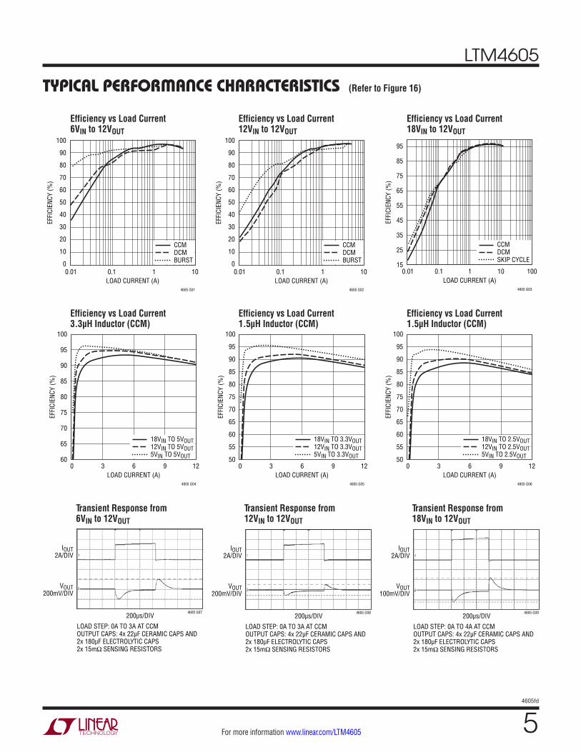
typical perForMance characteristics (Refer to Figure 16)
LOAD CURRENT (A)0
EFFI
CIEN
CY (%
)
3 6 129
4605 G06
18VIN TO 2.5VOUT12VIN TO 2.5VOUT5VIN TO 2.5VOUT
95
100
85
75
90
80
70
65
50
55
60
LOAD CURRENT (A)0.01
EFFI
CIEN
CY (%
)
100
90
80
70
60
50
40
30
20
10
00.1 1 10
4605 G02
CCMDCMBURST
LOAD CURRENT (A)0.01
EFFI
CIEN
CY (%
)
100
90
80
70
60
50
40
30
20
10
00.1 1 10
4605 G01
CCMDCMBURST
LOAD CURRENT (A)0.01
EFFI
CIEN
CY (%
)
0.1 1 10010
4605 G03
CCMDCMSKIP CYCLE
95
85
75
65
55
45
35
25
15
LOAD CURRENT (A)0
EFFI
CIEN
CY (%
)
3 6 129
4605 G04
18VIN TO 5VOUT12VIN TO 5VOUT5VIN TO 5VOUT
95
100
85
75
90
80
70
65
60
LOAD CURRENT (A)0
EFFI
CIEN
CY (%
)
3 6 129
4605 G05
18VIN TO 3.3VOUT12VIN TO 3.3VOUT5VIN TO 3.3VOUT
95
100
85
75
90
80
70
65
50
55
60
Efficiency vs Load Current 6VIN to 12VOUT
Efficiency vs Load Current 12VIN to 12VOUT
Efficiency vs Load Current 18VIN to 12VOUT
Efficiency vs Load Current 3.3µH Inductor (CCM)
Efficiency vs Load Current 1.5µH Inductor (CCM)
Efficiency vs Load Current 1.5µH Inductor (CCM)
Transient Response from 6VIN to 12VOUT
Transient Response from 12VIN to 12VOUT
Transient Response from 18VIN to 12VOUT
LOAD STEP: 0A TO 3A AT CCMOUTPUT CAPS: 4x 22µF CERAMIC CAPS AND2x 180µF ELECTROLYTIC CAPS2x 15mΩ SENSING RESISTORS
200µs/DIV4605 G07
IOUT2A/DIV
VOUT200mV/DIV
LOAD STEP: 0A TO 3A AT CCMOUTPUT CAPS: 4x 22µF CERAMIC CAPS AND2x 180µF ELECTROLYTIC CAPS2x 15mΩ SENSING RESISTORS
200µs/DIV4605 G08
IOUT2A/DIV
VOUT200mV/DIV
LOAD STEP: 0A TO 4A AT CCMOUTPUT CAPS: 4x 22µF CERAMIC CAPS AND2x 180µF ELECTROLYTIC CAPS2x 15mΩ SENSING RESISTORS
200µs/DIV4605 G09
IOUT2A/DIV
VOUT100mV/DIV
LTM4605
64605fd
For more information www.linear.com/LTM4605
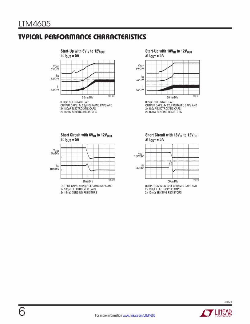
0.22µF SOFT-START CAPOUTPUT CAPS: 4x 22µF CERAMIC CAPS AND2x 180µF ELECTROLYTIC CAPS2x 15mΩ SENSING RESISTORS
50ms/DIV4605 G10
IIN5A/DIV
IL5A/DIV
VOUT5V/DIV
0.22µF SOFT-START CAPOUTPUT CAPS: 4x 22µF CERAMIC CAPS AND2x 180µF ELECTROLYTIC CAPS2x 15mΩ SENSING RESISTORS
50ms/DIV4605 G11
IIN2A/DIV
IL5A/DIV
VOUT5V/DIV
typical perForMance characteristics
Start-Up with 6VIN to 12VOUT at IOUT = 5A
Start-Up with 18VIN to 12VOUT at IOUT = 5A
Short Circuit with 6VIN to 12VOUT at IOUT = 5A
Short Circuit with 18VIN to 12VOUT at IOUT = 5A
OUTPUT CAPS: 4x 22µF CERAMIC CAPS AND2x 180µF ELECTROLYTIC CAPS2x 15mΩ SENSING RESISTORS
20µs/DIV4605 G12
IIN10A/DIV
VOUT5V/DIV
OUTPUT CAPS: 4x 22µF CERAMIC CAPS AND2x 180µF ELECTROLYTIC CAPS2x 15mΩ SENSING RESISTORS
100µs/DIV4605 G13
IIN5A/DIV
VOUT10V/DIV
LTM4605
74605fd
For more information www.linear.com/LTM4605
pin FunctionsVIN (Bank 1): Power Input Pins. Apply input voltage be-tween these pins and PGND pins. Recommend placing input decoupling capacitance directly between VIN pins and PGND pins.
VOUT (Bank 5): Power Output Pins. Apply output load between these pins and PGND pins. Recommend placing output decoupling capacitance directly between these pins and PGND pins.
PGND (Bank 6): Power Ground Pins for Both Input and Output Returns.
SW1, SW2 (Bank 4, Bank 2): Switch Nodes. The power inductor is connected between SW1 and SW2.
RSENSE (Bank 3): Sensing Resistor Pin. The sensing resis-tor is connected from this pin to PGND.
SENSE+ (Pin A4): Positive Input to the Current Sense and Reverse Current Detect Comparators.
SENSE– (Pin A5): Negative Input to the Current Sense and Reverse Current Detect Comparators.
EXTVCC (Pin F6): External VCC Input. When EXTVCC exceeds 5.7V, an internal switch connects this pin to INTVCC and shuts down the internal regulator so that the controller and gate drive power is drawn from EXTVCC. Do not exceed 7V at this pin and ensure that EXTVCC < VIN.
INTVCC (Pin F5): Internal 6V Regulator Output. This pin is for additional decoupling of the 6V internal regulator.
PLLIN (Pin B9): External Clock Synchronization Input to the Phase Detector. This pin is internally terminated to SGND with a 50k resistor. The phase-locked loop will force the rising bottom gate signal of the controller to be synchronized with the rising edge of PLLIN signal.
PLLFLTR (Pin B8): The lowpass filter of the phase-locked loop is tied to this pin. This pin can also be used to set the frequency of the internal oscillator with an AC or DC volt-age. See the Applications Information section for details.
SS (Pin A6): Soft-Start Pin. Soft-start reduces the input power sources’ surge currents by gradually increasing the controller’s current limit.
STBYMD (Pin A10): LDO Control Pin. Determine whether the internal LDO remains active when the controller is shut down. See Operations section for details. If the STBYMD pin is pulled to ground, the SS pin is internally pulled to ground to disable start-up and thereby providing a single control pin for turning off the controller. An internal de-coupling capacitor is tied to this pin.
VFB (Pin B6): The Negative Input of the Error Amplifier. Internally, this pin is connected to VOUT with a 100k preci-sion resistor. Different output voltages can be programmed with an additional resistor between VFB and SGND pins. See the Applications Information section.
FCB (Pin A9): Forced Continuous Control Input. The voltage applied to this pin sets the operating mode of the module. When the applied voltage is less than 0.8V, the forced continuous current mode is active. When this pin is allowed to float, the Burst Mode operation is active in boost operation and the skip cycle mode is active in buck operation. When the pin is tied to INTVCC, the constant frequency discontinuous current mode is active in buck or boost operation. See the Applications Information section.
SGND (Pin A7): Signal Ground Pin. This pin connects to PGND at output capacitor point.
COMP (Pin B7): Current Control Threshold and Error Amplifier Compensation Point. The current comparator threshold increases with this control voltage. The voltage ranges from 0V to 2.4V.
PGOOD (Pin B5): Output Voltage Power Good Indicator. Open drain logic output that is pulled to ground when the output voltage is not within ±7.5% of the regulation point.
RUN (Pin A8): Run Control Pin. A voltage below 1.6V will turn off the module. There is a 100k resistor between the RUN pin and SGND in the module. Do not apply more than 6V to this pin. See Applications Information section.

LTM4605
84605fd
For more information www.linear.com/LTM4605
siMpliFieD block DiagraM
SYMBOL PARAMETER CONDITIONS MIN TYP MAX UNITS
CIN External Input Capacitor Requirement (VIN = 4.5V to 20V, VOUT = 12V)
IOUT = 5A 10 µF
COUT External Output Capacitor Requirement (VIN = 4.5V to 20V, VOUT = 12V)
IOUT = 5A 200 300 µF
TA = 25°C. Use Figure 1 configuration.Decoupling requireMents
Figure 1. Simplified LTM4605 Block Diagram
EXTVCC
INTVCC
PGOOD
PLLIN
RUNON/OFF
STBYMD
M1
4605 BD
SW2
4.5V TO 20V
SW1
L
VIN
CIN
CONTROLLER
C1
100k
0.1µF
FCB
TO PGND PLANE AS SHOWN IN FIGURE 13
1000pF
SSSS
0.1µF
M2
COMP
M3
12V5A
VFB
RSENSE
VOUT
COUT
CO1
M4
100k RFB7.15k
RSENSE
INTCOMP
PLLFLTR
INTFILTER
INTFILTER
PGND
SGND
SENSE–
SENSE+

LTM4605
94605fd
For more information www.linear.com/LTM4605
operationPower Module Description
The LTM4605 is a non-isolated buck-boost DC/DC power supply. It can deliver a wide range output voltage from 0.8V to 16V over a wide input range from 4.5V to 20V, by only adding the sensing resistor, inductor and some external input and output capacitors. It provides precisely regulated output voltage programmable via one external resistor. The typical application schematic is shown in Figure 16.
The LTM4605 has an integrated current mode buck-boost controller, ultralow RDS(ON) FETs with fast switching speed and integrated Schottky diodes. With current mode control and internal feedback loop compensation, the LTM4605 module has sufficient stability margins and good transient performance under a wide range of operating conditions and with a wide range of output capacitors. The operating frequency of the LTM4605 can be adjusted from 200kHz to 400kHz by setting the voltage on the PLLFLTR pin.
Alternatively, its frequency can be synchronized by the input clock signal from the PLLIN pin. The typical switch-ing frequency is 400kHz.
The Burst Mode and skip-cycle mode operations can be enabled at light loads in the LTM4605 to improve its efficiency, while the forced continuous mode and discon-tinuous mode operations are used for constant frequency applications. Foldback current limiting is activated in an overcurrent condition as VFB drops. Internal overvoltage and undervoltage comparators pull the open-drain PGOOD output low if the output feedback voltage exits the ±10% window around the regulation point. Pulling the RUN pin below 1.6V forces the controller into its shutdown state.
If an external bias supply is applied on the EXTVCC pin, then an efficiency improvement will occur due to the re-duced power loss in the internal linear regulator. This is especially true at the higher input voltage range.
applications inForMation
The typical LTM4605 application circuit is shown in Figure 16. External component selection is primarily determined by the maximum load current and output voltage. Refer to Table 3 for specific external capacitor requirements for a particular application.
Output Voltage Programming
The PWM controller has an internal 0.8V reference voltage. As shown in the Block Diagram, a 100k, internal feedback resistor connects VOUT and VFB pins together. Adding a resistor RFB from the VFB pin to the SGND pin programs the output voltage:
VOUT = 0.8V • 100k +RFB
RFB
Table 1. RFB Resistor (0.5%) vs Various Output VoltagesVOUT 0.8V 1.5V 2.5V 3.3V 5V 6V
RFB Open 115k 47.5k 32.4k 19k 15.4k
VOUT 8V 9V 10V 12V 15V 16V
RFB 11k 9.76k 8.66k 7.15k 5.62k 5.23k
Operation Frequency Selection
The LTM4605 uses current mode control architecture at constant switching frequency, which is determined by the internal oscillator’s capacitor. This internal capacitor is charged by a fixed current plus an additional current that is proportional to the voltage applied to the PLLFLTR pin.

LTM4605
104605fd
For more information www.linear.com/LTM4605
applications inForMationThe PLLFLTR pin can be grounded to lower the frequency to 200kHz or tied to 2.4V to yield approximately 400kHz. When PLLFLTR is left open, the PLLFLTR pin goes low, forcing the oscillator to its minimum frequency.
A graph for the voltage applied to the PLLFLTR pin vs frequency is given in Figure 2. As the operating frequency increases, the gate charge losses will be higher, thus the efficiency is lower. The maximum switching frequency is approximately 400kHz.
FREqUENCY SYNCHRONIzATION
The LTM4605 can also be synchronized to an external source via the PLLIN pin instead of adjusting the voltage on the PLLFLTR pin directly. The power module has a phase-locked loop comprised of an internal voltage controlled oscillator and a phase detector. This allows turning on the internal top MOSFET for locking to the rising edge of the external clock. A pulse detection circuit is used to detect a clock on the PLLIN pin to turn on the phase-locked loop. The input pulse width of the clock has to be at least 400ns, and 2V in amplitude. The synchronized frequency ranges from 200kHz to 400kHz, corresponding to a DC voltage input from 0V to 2.4V at PLLFLTR. During the start-up of the regulator, the phase-locked loop function is disabled.
Low Current Operation
To improve the efficiency at low output current operation, LTM4605 provides three modes for both buck and boost operations by accepting a logic input on the FCB pin.
Figure 2. Frequency vs PLLFLTR Pin Voltage
PLLFLTR PIN VOLTAGE (V)0 0.5
OPER
ATIN
G FR
EQUE
NCY
(kHz
)
2.0
450
400
350
300
250
200
150
100
50
0
4605 F02
1.0 1.5 2.5
Table 2 shows the different operation modes.
Table 2. Different Operating ModesFCB PIN BUCK BOOST
0V to 0.75V Force Continuous Mode Force Continuous Mode
0.85V to VINTVCC – 1V
Skip-Cycle Mode Burst Mode Operation
>5.3V DCM with Constant Freq DCM with Constant Freq
When the FCB pin voltage is lower than 0.8V, the controller behaves as a continuous, PWM current mode synchronous switching regulator. When the FCB pin voltage is below VINTVCC – 1V, but greater than 0.85V, where VINTVCC is 6V, the controller enters Burst Mode operation in boost operation or enters skip-cycle mode in buck operation. During boost operation, Burst Mode operation is activated if the load current is lower than the preset minimum out-put current level. The MOSFETs will turn on for several cycles, followed by a variable “sleep” interval depending upon the load current. During buck operation, skip-cycle mode sets a minimum positive inductor current level. In this mode, some cycles will be skipped when the output load current drops below 1% of the maximum designed load in order to maintain the output voltage.
When the FCB pin is tied to the INTVCC pin, the controller enters constant frequency discontinuous current mode (DCM). For boost operation, if the output voltage is high enough, the controller can enter the continuous current buck mode for one cycle to discharge inductor current. In the following cycle, the controller will resume DCM boost operation. For buck operation, constant frequency discontinuous current mode is turned on if the preset minimum negative inductor current level is reached. At very light loads, this constant frequency operation is not as efficient as Burst Mode operation or skip-cycle, but does provide low noise, constant frequency operation.
Input Capacitors
In boost mode, since the input current is continuous, only minimum input capacitors are required. However, the input current is discontinuous in buck mode, so the selection of input capacitor CIN is driven by the need of filtering the input square wave current.

LTM4605
114605fd
For more information www.linear.com/LTM4605
applications inForMationFor a buck converter, the switching duty-cycle can be estimated as:
D =
VOUTVIN
Without considering the inductor current ripple, the RMS current of the input capacitor can be estimated as:
ICIN(RMS) =
IOUT(MAX)
η• D • (1−D)
In the above equation, η is the estimated efficiency of the power module. CIN can be a switcher-rated electrolytic aluminum capacitor, OS-CON capacitor or high volume ceramic capacitors. Note the capacitor ripple current rat-ings are often based on temperature and hours of life. This makes it advisable to properly derate the input capacitor, or choose a capacitor rated at a higher temperature than required. Always contact the capacitor manufacturer for derating requirements.
Output Capacitors
In boost mode, the discontinuous current shifts from the input to the output, so the output capacitor COUT must be capable of reducing the output voltage ripple.
For boost and buck modes, the steady ripple due to charg-ing and discharging the bulk capacitance is given by:
VRIPPLE,BOOST =
IOUT(MAX) • VOUT − VIN(MIN)( )COUT • VOUT • f
VRIPPLE,BUCK =
VOUT • VIN(MAX) − VOUT( )8 •L •COUT • VIN(MAX) • f2
The steady ripple due to the voltage drop across the ESR (effective series resistance) is given by:
VESR,BUCK = ΔIL(MAX) •ESR
VESR,BOOST = IL(MAX) •ESR
The LTM4605 is designed for low output voltage ripple. The bulk output capacitors defined as COUT are chosen with low enough ESR to meet the output voltage ripple and transient requirements. COUT can be a low ESR tanta-lum capacitor, a low ESR polymer capacitor or a ceramic capacitor. Multiple capacitors can be placed in parallel to meet the ESR and RMS current handling requirements. The typical capacitance is 300µF. Additional output filtering may be required by the system designer, if further reduc-tion of output ripple or dynamic transient spike is required. Table 3 shows a matrix of different output voltages and output capacitors to minimize the voltage droop and overshoot at a current transient.
Inductor Selection
The inductor is chiefly decided by the required ripple cur-rent and the operating frequency. The inductor current ripple ΔIL is typically set to 20% to 40% of the maximum inductor current. In the inductor design, the worst cases in continuous mode are considered as follows:
LBOOST ≥
VIN • VOUT(MAX) − VIN( )VOUT(MAX) • f • IOUT(MAX) •Ripple%
LBUCK ≥
VOUT • VIN(MAX) − VOUT( )VIN(MAX) • f • IOUT(MAX) •Ripple%
where:
f is operating frequency, Hz
Ripple% is allowable inductor current ripple, %
VOUT(MAX) is maximum output voltage, V
VIN(MAX) is maximum input voltage, V
VOUT is output voltage, V
IOUT(MAX) is maximum output load current, A
The inductor should have low DC resistance to reduce the I2R losses, and must be able to handle the peak inductor current without saturation. To minimize radiated noise, use a toroid, pot core or shielded bobbin inductor. Please refer to Table 3 for the recommended inductors for dif-ferent cases.

LTM4605
124605fd
For more information www.linear.com/LTM4605
applications inForMationRSENSE Selection and Maximum Output Current
RSENSE is chosen based on the required inductor current. Since the maximum inductor valley current at buck mode is much lower than the inductor peak current at boost mode, different sensing resistors are suggested to use in buck and boost modes.
The current comparator threshold sets the peak of the inductor current in boost mode and the maximum inductor valley current in buck mode. In boost mode, the allowed maximum average load current is:
IOUT(MAX,BOOST) =
160mVRSENSE
−ΔIL2
⎛
⎝⎜
⎞
⎠⎟ •
VINVOUT
where ΔIL is peak-to-peak inductor ripple current.
In buck mode, the allowed maximum average load cur-rent is:
IOUT(MAX,BUCK) =
130mVRSENSE
+ΔIL2
The maximum current sensing RSENSE value for the boost mode is:
RSENSE(MAX,BOOST) =
2 •160mV • VIN2 • IOUT(MAX,BOOST) • VOUT + ΔIL • VIN
The maximum current sensing RSENSE value for the buck mode is:
RSENSE(MAX,BUCK) =
2 •130mV2 • IOUT(MAX,BUCK) – ΔIL
A 20% to 30% margin on the calculated sensing resistor is usually recommended. Please refer to Table 3 for the recommended sensing resistors for different applications.
Soft-Start
The SS pin provides a means to soft-start the regulator. A capacitor on this pin will program the ramp rate of the output voltage. A 1.7µA current source will charge up the external soft-start capacitor. This will control the ramp
of the internal reference and the output voltage. The total soft-start time can be calculated as:
tSOFTSTART =
2.4V •CSS1.7µA
When the RUN pin falls below 1.6V, then soft-start pin is reset to allow for proper soft-start control when the regulator is enabled again. Current foldback and force continuous mode are disabled during the soft-start pro-cess. The soft-start function can also be used to control the output ramp up time, so that another regulator can be easily tracked. Do not apply more than 6V to the SS pin.
Run Enable
The RUN pin is used to enable the power module. The pin can be driven with a logic input, and not exceed 6V.
The RUN pin can also be used as an undervoltage lockout (UVLO) function by connecting a resistor from the input supply to the RUN pin. The equation:
V _UVLO =
R+100k100k
•1.6V
Power Good
The PGOOD pin is an open drain pin that can be used to monitor valid output voltage regulation. This pin monitors a ±7.5% window around the regulation point, and tracks with margining.
COMP Pin
This pin is the external compensation pin. The module has already been internally compensated for most output voltages. A spice model is available for other control loop optimization.
Fault Conditions: Current Limit and Overcurrent Foldback
LTM4605 has a current mode controller, which inherently limits the cycle-by-cycle inductor current not only in steady state operation, but also in transient. Refer to Table 3.
To further limit current in the event of an overload condi-tion, the LTM4605 provides foldback current limiting. If the
LTM4605
134605fd
For more information www.linear.com/LTM4605
applications inForMationoutput voltage falls by more than 70%, then the maximum output current is progressively lowered to about 30% of its full current limit value for boost mode and about 40% for buck mode.
Standby Mode (STBYMD)
The standby mode (STBYMD) pin provides several choices for start-up and standby operational modes. If the pin is pulled to ground, the SS pin is internally pulled to ground, preventing start-up and thereby providing a single control pin for turning off the controller. If the pin is left open or decoupled with a capacitor to ground, the SS pin is internally provided with a starting current, permitting external control for turning on the controller. If the pin is connected to a voltage greater than 1.25V, the internal regulator (INTVCC) will be on even when the controller is shut down (RUN pin voltage <1.6V). In this mode, the onboard 6V linear regulator can provide power to keep-alive functions such as a keyboard controller.
INTVCC and EXTVCC
An internal P-channel low dropout regulator produces 6V at the INTVCC pin from the VIN supply pin. INTVCC powers the control chip and internal circuitry within the module.
The LTM4605 also provides the external supply voltage pin EXTVCC. When the voltage applied to EXTVCC rises above 5.7V, the internal regulator is turned off and an internal switch connects the EXTVCC pin to the INTVCC pin thereby supplying internal power. The switch remains closed as long as the voltage applied to EXTVCC remains above 5.5V. This allows the MOSFET driver and control power to be derived from the output when (5.7V < VOUT < 7V) and from the internal regulator when the output is out of regulation (start-up, short-circuit). If more current is required through the EXTVCC switch than is specified, an external Schottky diode can be interposed between the EXTVCC and INTVCC pins. Ensure that EXTVCC ≤ VIN.
The following list summarizes the three possible connec-tions for EXTVCC:
1. EXTVCC left open (or grounded). This will cause INTVCC to be powered from the internal 6V regulator at the cost of a small efficiency penalty.
2. EXTVCC connected directly to VOUT (5.7V < VOUT < 7V). This is the normal connection for a 6V regulator and provides the highest efficiency.
3. EXTVCC connected to an external supply. If an external supply is available in the 5.5V to 7V range, it may be used to power EXTVCC provided it is compatible with the MOSFET gate drive requirements.
Thermal Considerations and Output Current Derating
In different applications, the LTM4605 operates in a variety of thermal environments. The maximum output current is limited by the environmental thermal condition. Sufficient cooling should be provided to ensure reliable operation. When the cooling is limited, proper output current derating is necessary, considering ambient temperature, airflow, input/output condition, and the need for increased reliability.
The power loss curves in Figures 5 and 6 can be used in coordination with the load current derating curves in Figures 7 to 12 for calculating an approximate θJA for the module. Column designation delineates between no heat sink, and a BGA heat sink. Each of the load current derating curves will lower the maximum load current as a function of the increased ambient temperature to keep the maximum junction temperature of the power module at 115°C maximum. This will allow a safe margin to work at the maximum operating temperature below 125°C. Each of the derating curves and the power loss curve that corresponds to the correct output voltage can be used to solve for the approximate θJA of the condition.
DESIGN EXAMPLES
Buck Mode Operation
As a design example, use input voltage VIN = 12V to 20V, VOUT = 12V and f = 400kHz.
Set the PLLFLTR pin at 2.4V or more for 400kHz frequency and connect FCB to ground for continuous current mode operation. If a divider is used to set the frequency as shown in Figure 14, the bottom resistor R3 is recommended not to exceed 1k.

LTM4605
144605fd
For more information www.linear.com/LTM4605
applications inForMationTo set the output voltage at 12V, the resistor RFB from VFB pin to ground should be chosen as:
RFB =
0.8V •100kVOUT − 0.8V
≈ 7.15k
To choose a proper inductor, we need to know the current ripples at different input voltages. The inductor should be chosen by considering the worst case in the practi-cal operating region. If the maximum output power P is 150W at buck mode, we can get the current ripple ratio of the current ripple ΔIL to the maximum inductor current IL as follows:
ΔILIL
=(VIN – VOUT ) • VOUT
2
VIN •L • f •P
Figure 3 shows the current ripple ratio at different input voltages based on the inductor values: 1.5µH, 2.5µH, 3.3µH and 4.7µH. If we need 30% ripple current ratio at all inputs, the 3.3µH inductor can be selected.
Consider the safety margin about 30%, we can choose the sensing resistor as 8mΩ.
For the input capacitor, use a low ESR sized capacitor to handle the maximum RMS current. Input capacitors are required to be placed adjacent to the module. In Fig-ure 14, the 10µF ceramic input capacitors are selected for their ability to handle the large RMS current into the converter. The 100µF bulk capacitor is only needed if the input source impedance is compromised by long inductive leads or traces.
For the output capacitor, the output voltage ripple and transient requirements require low ESR capacitors. If assuming that the ESR dominates the output ripple, the output ripple is as follows:
ΔVOUT(P-P) = ESR •ΔIL
If a total low ESR of about 5mΩ is chosen for output capacitors, the maximum output ripple of 17.5mV occurs at the input voltage of 20V with the current ripple at 3.5A.
Boost Mode Operation
For boost mode operation, use input voltage VIN = 5V to 12V, VOUT = 12V and f = 400kHz.
Set the PLLFLTR pin and RFB as in buck mode.
If the maximum output power P is 60W at boost mode and the module efficiency η is about 95%, we can get the current ripple ratio of the current ripple ΔIL to the maximum inductor current IL as follows:
ΔILIL
=(VOUT − VIN) • VIN
2 η
VOUT •L • f •P
Figure 4. shows the current ripple ratio at different input voltages based on the inductor values: 1.5µH, 2.5µH, 3.3µH and 4.7µH. If we need 30% ripple current ratio at all inputs, the 3.3µH inductor can be selected.
At buck mode, sensing resistor selection is based on the maximum output current and the allowed maximum sensing threshold 130mV.
RSENSE =
2 •130mV2 • (P / VOUT )− ΔIL
Figure 3. Current Ripple Ratio at Different Inputs for Buck Mode
INPUT VOLTAGE VIN (V)12 14
CURR
ENT
RIPP
LE R
ATIO
0.8
0.6
1.5µH
2.5µH
3.3µH
4.7µH
0.4
0.2
0
4605 F03
16 18 20
VOUT = 12Vƒ = 400kHz

LTM4605
154605fd
For more information www.linear.com/LTM4605
applications inForMation
At boost mode, sensing resistor selection is based on the maximum input current and the allowed maximum sensing threshold 160mV.
RSENSE =2 •160mV
2 • Pη • VIN(MIN)
+ ΔIL
Consider the safety margin about 30%, we can choose the sensing resistor as 7mΩ.
For the input capacitor, only minimum capacitors are needed to handle the maximum RMS current, since it is a continuous input current at boost mode. A 100µF capacitor is only needed if the input source impedance is compromised by long inductive leads or traces.
Since the output capacitors at boost mode need to filter the square wave current, more capacitors are expected to achieve the same output ripples as the buck mode. If assuming that the ESR dominates the output ripple, the output ripple is as follows:
ΔVOUT(P-P) = ESR • IL(MAX)
Figure 4. Current Ripple Ratio at Different Inputs for Boost Mode
INPUT VOLTAGE VIN (V)5 7
CURR
ENT
RIPP
LE R
ATIO
0.6
1.5µH
2.5µH
3.3µH
4.7µH
0.4
0.2
0
4605 F04
9 11 126 8 10
VOUT = 12Vƒ = 400kHz
If a total low ESR about 5mΩ is chosen for output capaci-tors, the maximum output ripple of 70mV occurs at the input voltage of 5V with the peak inductor current at 14A.
Wide Input Mode Operation
If a wide input range is required from 5V to 20V, the mod-ule will work in different operation modes. If input voltage VIN = 5V to 20V, VOUT = 12V and f = 400kHz, the design needs to consider the worst case in buck or boost mode design. Therefore, the maximum output power is limited to 60W. The sensing resistor is chosen at 7mΩ, the input capacitor is the same as the buck mode design and the output capacitor uses the boost mode design. Since the maximum output ripple normally occurs at boost mode in the wide input mode design, more inductor ripple cur-rent, up to 150% of the inductor current, is allowed at buck mode to meet the ripple design requirement. Thus, a 3.3µH inductor is chosen at the wide input mode. The maximum output ripple voltage is still 70mV if the total ESR is about 5mΩ.
Additionally, the current limit may become very high when the module runs at buck mode due to the low sensing resistor used in the wide input mode operation.
Safety Considerations
The LTM4605 modules do not provide isolation from VIN to VOUT. There is no internal fuse. If required, a slow blow fuse with a rating twice the maximum input current needs to be provided to protect each unit from catastrophic failure.
LTM4605
164605fd
For more information www.linear.com/LTM4605
applications inForMationTable 3. Typical Components (f = 400kHz)COUT1 VENDORS PART NUMBER COUT2 VENDORS PART NUMBER
TDK C4532X7R1E226M (22µF, 25V) Sanyo 16SVP180MX (180µF, 16V)
INDUCTOR VENDORS PART NUMBER RSENSE VENDORS PART NUMBER
Toko FDA1254 Vishay Power Metal Strip Resistors WSL1206-18
Sumida CDEP134, CDEP145 Panasonic Thick Film Chip Resistors ERJ12
VIN (V)
VOUT (V)
RSENSE (0.5W RATING)
Inductor (µH)
CIN (CERAMIC)
CIN (BULK)
COUT1 (CERAMIC)
COUT2 (BULK)
IOUT(MAX)* (A)
5 2.5 2x 16mΩ 0.5W 1 3x 10µF 25V 150µF 35V 2x 22µF 25V 1x 180µF 16V 12
12 2.5 2x 18mΩ 0.5W 1.5 2x 10µF 25V 150µF 35V 2x 22µF 25V 1x 180µF 16V 12
5 3.3 2x 18mΩ 0.5W 1 3x 10µF 25V 150µF 35V 2x 22µF 25V 1x 180µF 16V 12
12 3.3 2x 18mΩ 0.5W 1.5 2x 10µF 25V 150µF 35V 2x 22µF 25V 1x 180µF 16V 12
12 5 2x 18mΩ 0.5W 2.2 3x 10µF 25V 150µF 35V 2x 22µF 25V 1x 180µF 16V 12
20 5 2x 18mΩ 0.5W 2.5 2x 10µF 25V 150µF 35V 2x 22µF 25V 1x 180µF 16V 12
5 8 2x 14mΩ 0.5W 1.5 None 150µF 35V 4x 22µF 25V 2x 180µF 16V 8
12 8 2x 18mΩ 0.5W 2.2 3x 10µF 25V 150µF 35V 2x 22µF 25V 2x 180µF 16V 12
20 8 2x 18mΩ 0.5W 3.3 3x 10µF 25V 150µF 35V 2x 22µF 25V 2x 180µF 16V 12
5 10 2x 16mΩ 0.5W 2.2 None 150µF 35V 4x 22µF 25V 2x 180µF 16V 6
15 10 2x 18mΩ 0.5W 2.2 3x 10µF 25V 150µF 35V 2x 22µF 25V 2x 180µF 16V 12
20 10 2x 18mΩ 0.5W 3.3 3x 10µF 25V 150µF 35V 2x 22µF 25V 2x 180µF 16V 12
6 12 2x 14mΩ 0.5W 2.2 None 150µF 35V 4x 22µF 25V 2x 180µF 16V 6
16 12 2x 16mΩ 0.5W 2.2 2x 10µF 25V 150µF 35V 2x 22µF 25V 2x 180µF 16V 12
20 12 2x 18mΩ 0.5W 3.3 3x 10µF 25V 150µF 35V 2x 22µF 25V 2x 180µF 16V 12
5 16 2x 15mΩ 0.5W 3.3 None 150µF 35V 4x 22µF 25V 2x 150µF 20V 3.5
8 16 2x 14mΩ 0.5W 3.3 None 150µF 35V 4x 22µF 25V 2x 150µF 20V 6
12 16 2x 12mΩ 0.5W 2.2 None 150µF 35V 4x 22µF 25V 2x 150µF 20V 10
20 16 2x 18mΩ 0.5W 2.2 2x 10µF 25V 150µF 35V 2x 22µF 25V 2x 150µF 20V 12
INDUCTOR MANUFACTURER WEBSITE PHONE NUMBER
Sumida www.sumida.com 408-321-9660
Toko www.toko.com 847-297-0070
SENSING RESISTOR MANUFACTURER WEBSITE PHONE NUMBER
Panasonic www.panasonic.com/industrial/components 949-462-1816
KOA www.koaspeer.com 814-362-5536
Vishay www.vishay.com 800-433-5700
*Maximum load current is based on the Linear Technology Demo board DC1198A at room temperature with natural convection. Poor board layout design may decrease the maximum load current.

LTM4605
174605fd
For more information www.linear.com/LTM4605
applications inForMation
AMBIENT TEMPERATURE (°C)25 35 45 55 65 75 85 95
MAX
IMUM
LOA
D CU
RREN
T (A
)
115105
4605 F07
5VIN TO 12VOUT WITH 0LFM5VIN TO 12VOUT WITH 200LFM5VIN TO 12VOUT WITH 400LFM
5
3
1
4
2
0
Figure 7. 5VIN to 12VOUT without Heat Sink Figure 8. 5VIN to 12VOUT with Heat Sink
Figure 9. 5VIN to 16VOUT without Heat Sink Figure 10. 5VIN to 16VOUT with Heat Sink
Figure 5. 5VIN Power Loss Figure 6. 20VIN Power Loss
OUTPUT CURRENT (A)0
POW
ER L
OSS
(W)
1 2 543
4605 F05
5VIN TO 12VOUT
5VIN TO 16VOUT
8
9
6
4
7
5
3
2
0
1
OUTPUT CURRENT (A)0
POW
ER L
OSS
(W)
2 124 6 8 10
4605 F06
20VIN TO 12VOUT8
6
4
7
5
3
2
0
1
AMBIENT TEMPERATURE (°C)25 45 65 85
MAX
IMUM
LOA
D CU
RREN
T (A
)
125105
4605 F08
5VIN TO 12VOUT WITH 0LFM5VIN TO 12VOUT WITH 200LFM5VIN TO 12VOUT WITH 400LFM
5
3
1
4
2
0
AMBIENT TEMPERATURE (°C)25 35 45 55 65 75 85 95
MAX
IMUM
LOA
D CU
RREN
T (A
)
105
4605 F09
5VIN TO 16VOUT WITH 0LFM5VIN TO 16VOUT WITH 200LFM5VIN TO 16VOUT WITH 400LFM
4.0
3.0
1.0
0.5
3.5
2.0
1.5
2.5
0
AMBIENT TEMPERATURE (°C)25 35 45 55 65 75 85 95
MAX
IMUM
LOA
D CU
RREN
T (A
)
105
4605 F10
5VIN TO 16VOUT WITH 0LFM5VIN TO 16VOUT WITH 200LFM5VIN TO 16VOUT WITH 400LFM
4.0
3.0
1.0
0.5
3.5
2.0
1.5
2.5
0
Power loss includes all external components

LTM4605
184605fd
For more information www.linear.com/LTM4605
Table 4. 5V OutputDERATING CURVE VIN (V) POWER LOSS CURVE AIR FLOW (LFM) HEAT SINK θJA (°C/W)*
Figure 7, 9 12, 16 Figure 5 0 None 11.2
Figure 7, 9 12, 16 Figure 5 200 None 8.3
Figure 7, 9 12, 16 Figure 5 400 None 7.2
Figure 8, 10 12, 16 Figure 5 0 BGA Heat Sink 10.7
Figure 8, 10 12, 16 Figure 5 200 BGA Heat Sink 7.7
Figure 8, 10 12, 16 Figure 5 400 BGA Heat Sink 6.6
Table 5. 20V Input and 12V OutputDERATING CURVE VIN (V) POWER LOSS CURVE AIR FLOW (LFM) HEAT SINK θJA (°C/W)*
Figure 11 20 Figure 6 0 None 8.2
Figure 11 20 Figure 6 200 None 5.8
Figure 11 20 Figure 6 400 None 5.3
Figure 12 20 Figure 6 0 BGA Heat Sink 7.6
Figure 12 20 Figure 6 200 BGA Heat Sink 5.3
Figure 12 20 Figure 6 400 BGA Heat Sink 4.8
HEAT SINK MANUFACTURER PART NUMBER PHONE NUMBER
Wakefield Engineering LTN20069 603-635-2600
*The results of thermal resistance from junction to ambient θJA are based on the demo board of DC1198A. Thus, the maximum temperature on board is treated as the junction temperature (which is in the µModule for most cases) and the power losses from all components are counted for calculations. It has to be mentioned that poor board design may increase the θJA.
No Heat Sink BGA Heat Sink
AMBIENT TEMPERATURE (°C)35 45 55 65 75 85 95
MAX
IMUM
LOA
D CU
RREN
T (A
)
105
4605 F11
20VIN TO 12VOUT WITH 0LFM20VIN TO 12VOUT WITH 200LFM20VIN TO 12VOUT WITH 400LFM
12
8
10
4
2
6
0
AMBIENT TEMPERATURE (°C)35 45 55 65 75 85 95
MAX
IMUM
LOA
D CU
RREN
T (A
)
105
4605 F12
20VIN TO 12VOUT WITH 0LFM20VIN TO 12VOUT WITH 200LFM20VIN TO 12VOUT WITH 400LFM
12
8
10
4
2
6
0
Figure 11. 20VIN to 12VOUT without Heat Sink Figure 12. 20VIN to 12VOUT with Heat Sink
Power loss includes all external componentsapplications inForMation

LTM4605
194605fd
For more information www.linear.com/LTM4605
applications inForMationLayout Checklist/Example
The high integration of LTM4605 makes the PCB board layout very simple and easy. However, to optimize its electrical and thermal performance, some layout consid-erations are still necessary.
• Use large PCB copper areas for high current path, includ-ing VIN, RSENSE, SW1, SW2, PGND and VOUT. It helps to minimize the PCB conduction loss and thermal stress.
• Place high frequency input and output ceramic capaci-tors next to the VIN, PGND and VOUT pins to minimize high frequency noise
• Route SENSE– and SENSE+ leads together with minimum PC trace spacing. Avoid sense lines passing through noisy areas, such as switch nodes.
• Place a dedicated power ground layer underneath the unit.
• To minimize the via conduction loss and reduce module thermal stress, use multiple vias for interconnection between the top layer and other power layers
• Do not put vias directly on pads, unless the vias are capped.
• Use a separated SGND ground copper area for com-ponents connected to signal pins. Connect the SGND to PGND underneath the unit.
Figure 13. gives a good example of the recommended layout.
Figure 13. Recommended PCB Layout
VOUT
COUT
VIN
RSENSE
RSENSE
PGND
SW1
L1
SW2
PGNDSGND+
CIN
4605 F13
KELVIN CONNECTIONS TO RSENSE
–
LTM4605
204605fd
For more information www.linear.com/LTM4605
VOUTPGOOD
FCBRUN
SW1
SW2
EXTVCC
STBYMD
SS
VFBSGND
PLLIN
LTM4605
L13.3µH
RFB7.15k
22µF25Vx2
330µF25V
4605 TA03
VOUT12V5A
VIN
PGND
VIN4.5V TO 12V
C30.1µF
4.7µF35V
+ON/OFF
COMP
INTVCC
RSENSE
SENSE–
PLLFLTR
R27mΩ
2Ω
SENSE+
2200pF
OPTIONALFOR LOW
SWITCHING NOISER31k
R11.5k
Figure 15. Boost Mode Operation with 4.5V to 12V Input
typical applications
Figure 14. Buck Mode Operation with 12V to 20V Input
VOUTPGOOD
FCBRUN
SW1
COMP
SW2
INTVCC
RSENSEEXTVCC
SENSE–
STBYMD
PLLFLTR
SS
VFBSGND
PLLIN
LTM4605
R28mΩ
L13.3µH
RFB7.15k
100µF25V
4605 TA02
VOUT12V12A
VIN
PGND
VIN12V TO 20V
C30.1µF
10µF35Vx2
+ON/OFF
SENSE+R31k
R11.5k

LTM4605
214605fd
For more information www.linear.com/LTM4605
typical applications
VOUTPGOOD
FCBRUN
SW1
SW2
EXTVCC
STBYMD
SS
VFBSGND
PLLIN
LTM4605L1
3.3µH
RFB7.15k
22µF25Vx2
330µF25V
4605 TA04
VOUT12V5A
VIN
PGND
VIN4.5V TO 20V
C30.1µF
10µF35Vx2 +
ON/OFF
COMP
INTVCC
RSENSE
SENSE–
PLLFLTR
R27mΩ
SENSE+R31k
R11.5k
Figure 16. Wide Input Mode with 4.5V to 20V Input, 12V at 5A Output
R31k
R11.5k
VOUTPGOOD
FCBRUN
SW1
SW2
EXTVCC
STBYMD
SS
VFBSGND
PLLIN
LTM4605L1
2.5µH
RFB19k
100µF25V
4605 TA05
VOUT5V12A
VIN
PGND
VIN4.5V TO 20V
C30.1µF
10µF35Vx2
2200pF
+ON/OFF
COMP
INTVCC
RSENSE
SENSE–
PLLFLTR
R28mΩ
SENSE+
2Ω OPTIONAL
Figure 17. 5V at 12A Design with Low Switching Noise (Optional)

LTM4605
224605fd
For more information www.linear.com/LTM4605
typical applications
Figure 18. Two-Phase Parallel, 12V at 10A Design
VOUTPGOOD
FCB
RUN
SW1COMP
SW2INTVCC
EXTVCC
STBYMD
SS
VFBSGND
PLLIN
LTM4605L2
3.3µH
C422µF×2
330µF25V
4605 TA06
CLOCK SYNC 180° PHASE
CLOCK SYNC 0° PHASE
VIN
PGND
10µF35V
+
VOUTPGOOD
FCBRUN
SW1COMP
SW2INTVCC
EXTVCC
PLLFLTR
PLLFLTR
OUT1V+
OUT2
MOD
GND
SET
LTC6908-1
200Ω
STBYMD
SS
VFBSGND
PLLIN
LTM4605L1
3.3µH
RFB3.57k
R4324k
C222µF×2
330µF25V
VOUT12V10A
2-PHASE OSCILLATOR
VIN
PGND
VIN4.5V TO 20V
C30.1µF
10µF35V
+R5100k
5.1VZENER
C10.1µF
RSENSE
SENSE–
R37mΩ
SENSE+
RSENSE
SENSE–
R27mΩ
SENSE+5.1V
Figure 19. Buck Mode Operation with Positive Input to Negative –5V Output Converter
LOAD CURRENT (A)0 1 2 3 4 5
EFFI
CIEN
CY (%
)
95
90
85
80
75
70
65
60
55
50
4605 TA08b
6
VIN = 6VVIN = 12VVIN = 15V
VOUT = –5V
Efficiency vs Load
VOUTPGOOD
FCBRUN
SW1
COMP
SW2
INTVCC
RSENSEEXTVCC
SENSE–
STBYMD
PLLFLTR
SS
VFBSGND
PLLIN
LTM4605
R28mΩ
L13.5µH
RFB19.1k
22µF16V×2
4605 TA08
GNDVIN
PGND
VIN6V TO 15V
C310nF
10µF35V×2
ON/OFF 180µF16V×2
+
SENSE+R31.21k
R14.64k
–5V –5V
–5V
–5V
–5V–5V
–5V
–5V

LTM4605
234605fd
For more information www.linear.com/LTM4605
package Description
LGA
Pack
age
141-
Lead
(15m
m ×
15m
m ×
2.8
2mm
)(R
efer
ence
LTC
DWG
# 05
-08-
1815
Rev
C)
Please refer to http://www.linear.com/designtools/packaging/ for the most recent package drawings.
NOTE
S:1.
DIM
ENSI
ONIN
G AN
D TO
LERA
NCIN
G PE
R AS
ME
Y14.
5M-1
994
2. A
LL D
IMEN
SION
S AR
E IN
MIL
LIM
ETER
S
LAN
D DE
SIGN
ATIO
N PE
R JE
SD M
O-22
2, S
PP-0
10
43
DETA
ILS
OF P
AD #
1 ID
ENTI
FIER
ARE
OPT
IONA
L,BU
T M
UST
BE L
OCAT
ED W
ITHI
N TH
E ZO
NE IN
DICA
TED.
THE
PAD
#1 ID
ENTI
FIER
MAY
BE
EITH
ER A
MOL
D OR
M
ARKE
D FE
ATUR
E
5PA
D #1
IDEN
TIFI
ER O
N TH
E PA
CKAG
E BO
TTOM
,CA
N BE
SHI
PPED
WIT
H OR
WIT
HOUT
A T
RIAN
GLE
MAR
KER.
6. P
RIM
ARY
DATU
M -Z
- IS
SEAT
ING
PLAN
E
7. T
HE T
OTAL
NUM
BER
OF P
ADS:
141
SYM
BOL
aaa
bbb
eee
TOLE
RANC
E0.
150.
100.
05
2.72
– 2
.92
DETA
IL B
DETA
IL C
DETA
IL B
SUBS
TRAT
EM
OLD
CAP
0.27
– 0
.37
2.45
– 2
.55
bbb Z
Z
15 BSC
PACK
AGE
TOP
VIEW
15 BSC
4PAD
1CO
RNER
XY
aaa
Z
aaa
Z
DETA
IL A
13.9
7BS
C 1.27
BSC
13.9
7BS
C
0.12
– 0
.28
PACK
AGE
BOTT
OM V
IEW
PAD
13
5
PADS
SEE
NOTE
S
DETA
IL A
0.63
0 ±0
.025
SQ.
141
x
SY
Xee
e
SUGG
ESTE
D PC
B LA
YOUT
TOP
VIEW
0.00
000.
6350
0.63
50
1.90
50
1.90
50
3.17
50
3.17
50
4.44
50
4.44
50
5.71
50
5.71
50
6.98
50
6.9850
6.9850
5.7150
5.7150
4.4450
4.4450
3.1750
3.1750
1.9050
1.9050
0.6350
0.63500.0000
6.98
50
LGA
141
1212
REV
C
LTM
XXXX
XXµM
odul
e
TRAY
PIN
1BE
VEL
PACK
AGE
IN T
RAY
LOAD
ING
ORIE
NTAT
ION
COM
PONE
NTPI
N “A
1”
L K J H G F E D C BM A
12
34
56
78
109
1112
DETA
IL C
8PA
CKAG
E RO
W A
ND C
OLUM
N LA
BELI
NG M
AY V
ARY
AMON
G µM
odul
e PR
ODUC
TS. R
EVIE
W E
ACH
PACK
AGE
LAYO
UT C
AREF
ULLY
!
8
SEE
NOTE
S

LTM4605
244605fd
For more information www.linear.com/LTM4605
package DescriptionPin Assignment Table 6
(Arranged by Pin Number)
PIN NAME PIN NAME PIN NAME PIN NAME PIN NAME PIN NAME
A1 PGND C1 PGND E1 VOUT G1 VOUT J1 SW1 L1 SW1
A2 PGND C2 PGND E2 VOUT G2 VOUT J2 SW1 L2 SW1
A3 PGND C3 PGND E3 PGND G3 VOUT J3 SW1 L3 SW1
A4 SENSE+ C4 PGND E4 PGND G4 VOUT J4 SW1 L4 SW1
A5 SENSE– C5 PGND E5 PGND G5 RSENSE J5 RSENSE L5 RSENSE
A6 SS C6 PGND E6 PGND G6 RSENSE J6 RSENSE L6 RSENSE
A7 SGND C7 PGND E7 PGND G7 RSENSE J7 RSENSE L7 SW2
A8 RUN C8 PGND E8 PGND G8 RSENSE J8 SW2 L8 SW2
A9 FCB C9 PGND E9 PGND G9 RSENSE J9 SW2 L9 SW2
A10 STBYMD C10 PGND E10 PGND G10 RSENSE J10 VIN L10 VIN
A11 PGND C11 PGND E11 PGND G11 RSENSE J11 VIN L11 VIN
A12 PGND C12 PGND E12 PGND G12 RSENSE J12 VIN L12 VIN
B1 PGND D1 PGND F1 VOUT H1 VOUT K1 SW1 M1 SW1
B2 PGND D2 PGND F2 VOUT H2 VOUT K2 SW1 M2 SW1
B3 PGND D3 PGND F3 VOUT H3 VOUT K3 SW1 M3 SW1
B4 PGND D4 PGND F4 VOUT H4 VOUT K4 SW1 M4 SW1
B5 PGOOD D5 PGND F5 INTVCC H5 RSENSE K5 RSENSE M5 RSENSE
B6 VFB D6 PGND F6 EXTVCC H6 RSENSE K6 RSENSE M6 RSENSE
B7 COMP D7 PGND F7 – H7 RSENSE K7 SW2 M7 SW2
B8 PLLFLTR D8 PGND F8 – H8 RSENSE K8 SW2 M8 SW2
B9 PLLIN D9 PGND F9 – H9 RSENSE K9 SW2 M9 SW2
B10 PGND D10 PGND F10 RSENSE H10 RSENSE K10 VIN M10 VIN
B11 PGND D11 PGND F11 RSENSE H11 RSENSE K11 VIN M11 VIN
B12 PGND D12 PGND F12 RSENSE H12 RSENSE K12 VIN M12 VIN

LTM4605
254605fd
For more information www.linear.com/LTM4605
Information furnished by Linear Technology Corporation is believed to be accurate and reliable. However, no responsibility is assumed for its use. Linear Technology Corporation makes no representa-tion that the interconnection of its circuits as described herein will not infringe on existing patent rights.
revision historyREV DATE DESCRIPTION PAGE NUMBER
C 01/11 Updated Absolute Maximum Ratings section.Updated Electrical Characteristics section.Updated the FCB Pin description in the Pin Functions section.Updated the Block Diagram.Updated the Applications Information section.Text added to Figures 3 and 4.Updated Figure 18.Added new Figure 19.Updated the Related Parts section.
22, 3, 4
78
9, 1014, 15
222226
D 04/14 Updated the Order Information table.Updated circuit schematics.
220-22
(Revision history begins at Rev C)
LTM4605
264605fd
For more information www.linear.com/LTM4605 LINEAR TECHNOLOGY CORPORATION 2007
LT 0414 REV D • PRINTED IN USALinear Technology Corporation1630 McCarthy Blvd., Milpitas, CA 95035-7417(408) 432-1900 FAX: (408) 434-0507 www.linear.com/LTM4605
typical application
relateD partsPART NUMBER DESCRIPTION COMMENTS
LTC2900 Quad Supply Monitor with Adjustable Reset Timer Monitors Four Supplies; Adjustable Reset Timer
LTC2923 Power Supply Tracking Controller Tracks Both Up and Down; Power Supply Sequencing
LTC3780 36V Buck-Boost Controller Synchronous Operation, Single Inductor
LTC3785 10V Buck-Boost Controller Synchronous Operation, No RSENSE™, 2.7V ≤ VIN ≤ 10V, 2.7V ≤ VOUT ≤ 10V
LTM4600 10A DC/DC µModule Regulator Basic 10A DC/DC µModule Regulator
LTM4601/ LTM4601A
12A DC/DC µModule Regulator with PLL, Output Tracking/ Margining and Remote Sensing
Synchronizable, PolyPhase® Operation to 48A, LTM4601-1 Version Has No Remote Sensing
LTM4618 6A DC/DC µModule Regulator with PLL and Output Tracking/Margining and Remote Sensing
Synchronizable, PolyPhase Operation
LTM4604A 4A Low Voltage DC/DC µModule Regulator 2.375 ≤ VIN ≤ 5V, 0.8V ≤ VOUT ≤ 5V, 9mm × 15mm × 2.3mm Package
LTM4608A 8A DC/DC µModule Regulator 2.7V to 5.5V Input, 0.6V to 5V Output, PLL, Tracking
VOUTPGOOD
FCBRUN
SW1
COMP
SW2
INTVCC
RSENSEEXTVCC
SENSE–
STBYMD
PLLFLTR
SS
VFBSGND
PLLIN
LTM4605
R28mΩ
L13.3µH
RFB7.15k
100µF25V
4605 TA07
VOUT12V12A
VIN
PGND
VIN12V TO 20V
C30.1µF
10µF35Vx2
+ON/OFF
SENSE+R31k
R11.5k
Buck Mode Operation with 12V to 20V Input