m2 - graphene on-chip thz
TRANSCRIPT

Universite Paris Diderot - Paris 7
M2 Quantum Devices
Internship report
Graphene on-chip terahertz time domainspectroscopy
Laboratoire Pierre Aigrain, ENS Ulm
Author
Thanh-Quy Nguyen
Supervisor
Dr. Juliette Mangeney
Reporter
Dr. Sara Ducci
June 27th, 2014
Acknowledgements
First, I would like to thank Dr. Sara Ducci, the head of the Quantum Devices Master’s Degree thanks to whom
I found this internship and so did everyone in our class. Her work enabled everyone to experience an immersion
in a lab, hopefully working on a topic of their taste. This internship wouldn’t have happened without the entire
Laboratoire Pierre Aigrain team, and more especially Dr. Juliette Mangeney. They accepted me for this internship
and Juliette Mangeney managed to always be available in spite of her incredible amount of work. She helped me not
only for the experiments, but also for my report and for my presentation.
My thanks go to Professor Jerome Tignon, who is the head of the Terahertz Team and without whom none of the
current experiments in the lab would exist. I also sincerely thank Dr. Sukhdeep Dhillon, a researcher I keep meeting
during my internships, may they be in England or in France.
A lot of thanks go the PhD student Matthieu Baillergeau, a young but talented physicist who has always been able
to answer any physical question. Jean Maysonnave, Feihu Wang, Sarah Houver are also thanked, not only for their
advice but for their presence which made the lab such a pleasant place to be. I wish good luck to all of them for the
end of their PhD, even if Jean will finish very soon. I thank Anaıs as well, who was here as an intern at the same
time than me but who will begin her PhD next year.
Some special thanks to my old friend Erik Lehnsherr, even if we didn’t end working in the same field.
Of course, I also thank Pascal Morfin and Jose Palomo who respectively trained me with the CVD and a few clean
room processes. I thank Dr. Kenneth Maussang for his relevant remarks and advice, almost as much as I thank
Djamal Eddine Gacemi for his work first, which helped a lot on writing this report, and for being available for
answering any question we would have had.
Last but not least, my most sincere thanks go to postdoctoral Anthony Brewer who not only directly supervised my
internship and trained me most of the time, but who also became a friend, even if he kind of spoiled me Game of
Thrones. A little.
Laboratoire Pierre Aigrain is specialised in condensed matter physics. It is a major actor of the field and its works
in optic properties of semi-conductive and metallic nanostructures, transport phenomena at a mesoscopic scale or
biophysics are recognised all around the world. The THz team is particularly known for its study of semiconductor
nanostructures using THz spectroscopy. Several setups are therefore used, such as a THz-TDS (Terahertz-Time
Domain Spectroscopy) or Quantum Cascade Lasers (QCLs).
ii

Abstract
Arguably the most important development to Terahertz spectroscopy to date is the demonstration of terahertz (THz)
time domain spectroscopy (TDS) with electro-optic (EO) sampling. Current state-of-the-art THz-TDS systems
employ free space optics with beam paths evacuated under vacuum, or purged with an inert gas, so to eliminate the
effect of water absorption and atmospheric losses in the beam path.
In this report we demonstrate a wholly-fibre-based time domain pump/probe THz spectroscopy system for on-chip
analysis. The fibre based approach is more robust than table top free space systems, eliminating tricky alignments
and better lends itself to industrial applications. Also, THz pulses propagate along waveguides in contrast to usual
free space TDS, eliminating the problem of diffraction limited spot size for free space systems.
The first chapter is a presentation of the state of the art and the scientific problems to solve. Theorical notions
necessary to the understanding of TDS are also introduced.
In chapter 2, we discuss the construction of low loss apparatus and the challenges involved in correcting the fibre
based dispersion of an 80 fs laser at 1550 nm wavelength. A full description of the experimental setup is given as
well as our original electro-optic probe.
Chapter 3 is about the characterisation of a 20 µm gap InGaAs photoswitch and on-chip analysis of propagating
THz field. Finally, we discuss preliminary investigations of pump/probe THz spectroscopy on monolayer graphene.
A significant advantage of our system over conventional THz-TDS is that the interaction length of the THz field
can be many tens or hundreds or micrometres, compared to just a few Angstroms with single-pass transmission of
reflection THz-TDS. Following on from the InGaAs analysis we introduce graphene samples: their growth, clean
room fabrication and electrical characterisation.
iii

Contents
Acknowledgements ii
Abstract iii
Contents iv
List of Figures vi
List of abreviations vii
1 Introduction 1
1.1 State of the Art . . . . . . . . . . . . . . . . . . . . . . . . . . . . . . . . . . . . . . . . . . . . . . . . . 1
1.2 Theory . . . . . . . . . . . . . . . . . . . . . . . . . . . . . . . . . . . . . . . . . . . . . . . . . . . . . . 2
1.2.1 Photoconductive switches . . . . . . . . . . . . . . . . . . . . . . . . . . . . . . . . . . . . . . . 2
1.2.2 Detection . . . . . . . . . . . . . . . . . . . . . . . . . . . . . . . . . . . . . . . . . . . . . . . . 2
1.2.3 THz-Time Domain Spectroscopy . . . . . . . . . . . . . . . . . . . . . . . . . . . . . . . . . . . 3
2 Experimental setup 5
2.1 Description . . . . . . . . . . . . . . . . . . . . . . . . . . . . . . . . . . . . . . . . . . . . . . . . . . . 5
2.1.1 Description of the arms . . . . . . . . . . . . . . . . . . . . . . . . . . . . . . . . . . . . . . . . 5
2.1.2 Electro-optic probe . . . . . . . . . . . . . . . . . . . . . . . . . . . . . . . . . . . . . . . . . . . 6
2.2 Optimisation . . . . . . . . . . . . . . . . . . . . . . . . . . . . . . . . . . . . . . . . . . . . . . . . . . 7
3 Measurements & Results 9
3.1 InGaAs photoswitches . . . . . . . . . . . . . . . . . . . . . . . . . . . . . . . . . . . . . . . . . . . . . 9
3.1.1 Electrical characterisation . . . . . . . . . . . . . . . . . . . . . . . . . . . . . . . . . . . . . . . 10
3.1.2 Delay line measurement . . . . . . . . . . . . . . . . . . . . . . . . . . . . . . . . . . . . . . . . 10
3.1.3 X measurements . . . . . . . . . . . . . . . . . . . . . . . . . . . . . . . . . . . . . . . . . . . . 11
3.1.4 Signal-to-noise ratio . . . . . . . . . . . . . . . . . . . . . . . . . . . . . . . . . . . . . . . . . . 12
3.2 Graphene photoswitches . . . . . . . . . . . . . . . . . . . . . . . . . . . . . . . . . . . . . . . . . . . . 13
3.2.1 Description . . . . . . . . . . . . . . . . . . . . . . . . . . . . . . . . . . . . . . . . . . . . . . . 13
iv
CONTENTS CONTENTS
3.2.2 Graphene growth and characterisation . . . . . . . . . . . . . . . . . . . . . . . . . . . . . . . . 14
3.2.3 Fabrication . . . . . . . . . . . . . . . . . . . . . . . . . . . . . . . . . . . . . . . . . . . . . . . 15
3.2.4 Electric characterisation . . . . . . . . . . . . . . . . . . . . . . . . . . . . . . . . . . . . . . . . 17
3.3 Expectations . . . . . . . . . . . . . . . . . . . . . . . . . . . . . . . . . . . . . . . . . . . . . . . . . . 18
Conclusion 19
Software credit ix
Bibliography x
v
List of Figures
1.1 Schematic of the electro-optic detection principle [12] . . . . . . . . . . . . . . . . . . . . . . . . . . . . 2
1.2 Effect of the dispersion on the pulse duration [12] . . . . . . . . . . . . . . . . . . . . . . . . . . . . . . 3
2.1 Schematic of the experimental setup . . . . . . . . . . . . . . . . . . . . . . . . . . . . . . . . . . . . . 5
2.2 Schematic of the electro-optic probe . . . . . . . . . . . . . . . . . . . . . . . . . . . . . . . . . . . . . 6
2.3 Electro-optic probe alignment . . . . . . . . . . . . . . . . . . . . . . . . . . . . . . . . . . . . . . . . . 8
3.1 Schematic of the gold striplines with InGaAs photoswitch . . . . . . . . . . . . . . . . . . . . . . . . . 9
3.2 I/V curve and photocurrent measurements . . . . . . . . . . . . . . . . . . . . . . . . . . . . . . . . . . 10
3.3 InGaAs THz pulse obtained by varying the delay line length . . . . . . . . . . . . . . . . . . . . . . . . 11
3.4 X scan of the InGaAs photoswitch . . . . . . . . . . . . . . . . . . . . . . . . . . . . . . . . . . . . . . 12
3.5 Horizontal sensitivity vs. vertical sensitivity of the electro-optic crystal . . . . . . . . . . . . . . . . . . 12
3.6 Potential signal-to-noise ratio as a function of the photocurrent . . . . . . . . . . . . . . . . . . . . . . 13
3.7 Schematic of our graphene-based photoswiches . . . . . . . . . . . . . . . . . . . . . . . . . . . . . . . 13
3.8 Topas® molecule . . . . . . . . . . . . . . . . . . . . . . . . . . . . . . . . . . . . . . . . . . . . . . . . 14
3.9 Graphene growth by CVD . . . . . . . . . . . . . . . . . . . . . . . . . . . . . . . . . . . . . . . . . . . 14
3.10 Raman spectroscopy result of a graphene on Topas sample . . . . . . . . . . . . . . . . . . . . . . . . . 15
3.11 Fabrication of photoswitches (1/2) . . . . . . . . . . . . . . . . . . . . . . . . . . . . . . . . . . . . . . 16
3.12 Fabrication of photoswitches (2/2) . . . . . . . . . . . . . . . . . . . . . . . . . . . . . . . . . . . . . . 16
3.13 Schematic representation of the graphene photoswitch put in the setup . . . . . . . . . . . . . . . . . 17
3.14 Measurement of the graphene sample photocurrent . . . . . . . . . . . . . . . . . . . . . . . . . . . . . 17
3.15 Result expectations for our graphene photoswitch . . . . . . . . . . . . . . . . . . . . . . . . . . . . . . 18
vi

List of abreviations
Al Aluminium
Au Gold
CVD Chemical Vapor Deposition
ENS Ecole Normale Superieure
Far-FTIR Far Infra-Red Fourier Transform
FFT Fast Fourier Transform
FIR Far Infra-Red
FWHM Full Width at Half Maximum
fs Femtosecond = 10−15 second
GaAs Gallium Arsenide
I/V Current/Voltage
InGaAs Indium Gallium Arsenide
InP Indium Phosphide
LPA Laboratoire Pierre Aigrain
LT-GaAs Low temperature grown gallium arsenide
n Refractive index
ps picosecond = 10−12 second
QCL Quantum Cascade Lasers
R Reflection index or carbon chain, depending on the situation
RF Radio frequency
RIE Reactive Ion Etching
THz Terahertz = 1012 Hertz
THz-TDS Terahertz Time Domain Spectroscopy
ZnTe Zinc Telluride
λ/4 plate Quarter-wave plate
vii

Chapter 1
Introduction
1.1 State of the Art
Efficient confinement of electromagnetic fields is a promising building block for both optic and electronic devices. For
optics especially, it is interesting for optic communications, optic IT and microelectronics/optics hybrid circuits. In
the THz domain (0.1 ∼ 10 THz), confinement of the electromagnetic energy has been a long time issue considering
the high wavelengths implying a diffraction limit around ∼ 150 µm. Classic imaging and spectroscopy techniques
are therefore unsuitable for the study of small objects. Yet, researchers show a keen interest in the study of these
small objects at the THz frequencies. Terahertz photons are able to excite rotations of molecules in their gas form,
vibrations of a whole molecule, alignment of dipoles in polar-molecule-based liquids such as water, optic and acoustic
phonons, free carriers in semi-conductive nanostructures or graphene. Resonances associated with these physical
phenomena are not easy to reach in near infrared, visible or UV domains. But most especially, terahertz confinement
is very promising for enabling smaller devices and integration of THz technologies.
In the optical domain, one way to confine electromagnetic waves at subwavelength scale is to couple them with
collective oscillations of free electrons in a metal. Surface waves, called Surface plasmon polaritons, originate from
this coupling. They propagate along the interface between metal and the surrounding dielectric medium with an
exponential decrease of the electric field along the propagation direction and the normal direction to the interface.
Confinement of these plasmons can reach several tens of nanometres in the visible domain and hundreds of nanometres
in the near infra-red with a propagation length of hundreds of micrometres. These surface plasmon polaritons
waveguides have been widely studied and may be the subjects of many applications in spectroscopy [1], nano-
photonics [2, 3], high resolution imaging [4], biological detection [5, 6] and integrated optics [7].
However, in the THz domain, coupling between electromagnetic waves and free electrons in a metal is very low
[8]. Therefore, no significant confinement of the surface electromagnetic wave results from it: THz electric field can
indeed go as far as tens of millimeters away from the interface metal/dielectric. To answer this problem, George J.
E. Goubau proposed in 1950 to modify the metal surface with a thin dielectric coating or surface structuring [9]. His
ideas have been experimented for a long time now: current works report confinement of THz surface waves of 0.5
mm in structured metal [10]. Alternative techniques have also been proposed, such as parallel metallic waveguides
which resulted in confinement of THz surface waves within 18 µm [11].
My work during my internship is the sequel of Dr. Gacemi’s works during his PhD [12, 13, 14]. My scientific objectives
were precisely to improve the setup he developed during his PhD by making it a fully-waveguided setup using optical
fibres. At the end, our objective was to generate and detect THz with a new sample based on parallel gold striplines
and a graphene layer at the top of a Topas substrate and map the propagation of the THz waves generated. Such
integrated metallic waveguides pave the way for THz chip, high resolution imaging, extreme focusing as well as
development of ultra-fast electronic circuits [15, 16, 17].
1

1.2. THEORY CHAPTER 1. INTRODUCTION
1.2 Theory
1.2.1 Photoconductive switches
The THz sources in our setup are all based on the photoconductive switch principle coupled with waveguides.
A photoconductive emitter is made of two electrodes separated by a few microns at the top of a photoconducting
material forming a photoconductive switch. When biased, the electrode contacts can be momentarily closed by
a short (< 150 fs) excitation laser pulse such that an intense transient current is generated and a subpicosecond
electromagnetic pulse with frequency components in the THz range is transmitted into free space from the switch
[18]. However, the electromagnetic pulse can be coupled to the free electrons of a metallic waveguide, confining the
THz pulses.
This is what happens with our photoswitches: a photoconducting material (InGaAs in section 3.1 and then graphene
in section 3.2) is subject to photoexcitation by a femtosecond laser. Carriers oscillate at THz frequencies by interband
(InGaAs) or intersubband (graphene) transition depending on the band structure of the photoconducting material
which creates a dipole. Coupled with metallic waveguides, the free electrons of the metal will also oscillate at the
same frequency allowing the THz wave to propagate.
1.2.2 Detection
Our detection system is based on electro-optic sampling detection. A schematic of the principle is available in
figure 1.1.
Figure 1.1 – Schematic of the electro-optic detection principle [12]
This represents the evolution of a laser beam polarisation through the different optical components which form the
electro-optic sampling:
� A laser beam with an unknown polarisation is going through the ZnTe crystal.
� Depending on the amplitude of the terahertz wave going through the crystal, a refractive index of the ZnTe
crystal changes. The polarisation of the incoming beam after the ZnTe crystal will therefore be elliptical.
� A quarter-waveplate will transform this elliptical polarisation into a linear one.
� After a half-waveplate, the beam’s polarisation is circular.
2

CHAPTER 1. INTRODUCTION 1.2. THEORY
� A Wollaston prism splits the beam into a two linear polarisation beams: one being vertical and the other being
horizontal.
� The two beams are sent into time-balanced photodiodes. The amplitude of these are then substracted to one
another, and the result is proportional to the THz electric field the ZnTe crystal was subject to [19]. It is also
the value we are interested in.
The balanced photodiodes are connected to a lock-in detection system in order to synchronise the detection with the
pulses generated by the laser.
1.2.3 THz-Time Domain Spectroscopy
A system which would enable us to detect the terahertz pulses generated by our photoswitches and using the electro-
optic detection is the THz-Time Domain Spectroscopy (THz-TDS). THz-TDS is a setup based on electro-optic
detection and a delay line thanks to which the entire width of the terahertz pulse can be explored.
Here is a description of the basic functioning of a THz-TDS system:
� A pulse laser beam is sent into a beam splitter, which is split in a probe beam and a pump beam.
� A pump beam excites a photoswitch which generates THz. The THz is then led into an electro-optic crystal.
� The probe beam goes through a delay line and directly to the electro-optic crystal. It then goes to the electro-
optic detection system described in section 1.2.2, which enables the measurement of the THz field amplitude.
Changing the length of the delay line for every pulse enables an exploration of the THz time domain.
� A Fast Fourier Transform (FFT) allows us to find the information of the constant THz pulse in the frequency
domain.
The usual THz-TDS systems are usually in free space, using photoconductive antenna, bow tie or interdigitated
antenna for example. THz waves are collected by parabolic mirrors. However, this technique is limited by the
diffraction which only enables analysis of objects of the size of the spot at minimum (∼ 150 µm). Our system, using
waveguides to propagate the THz, enables analysis of samples equal to the gap between the Au waveguide electrodes,
which could be just a few µm in size. We will also see that it allows us to map the propagation of the THz field.
However, in any case, chromatic dispersion problems exist and must be considered.
Figure 1.2 – Effect of the dispersion on the pulse duration [12]Simulated pulse dispersion, using Fiberdesk Simulation software, for an 80 fs pulse at 1550 nm propagating along
an SMF-28 fibre of increasing length. Simulation dots report calculation results by the software FiberDesk. Actualmeasure dots have been obtained by Djamal Gacemi.
3

1.2. THEORY CHAPTER 1. INTRODUCTION
Figure 1.2 [12] shows the effect of dispersion to the 80 fs laser pulse as it propagates along the optical fibers and is
elongated in time. Beause of the FFT involved in switching from the time to frequency domain, a very short duration
laser pulse is critical to achieving a large THz bandwidth.
Considering that our pump and probe arms (figure 2.1) are typically ∼ 3 m long, this would extent the duration
of the laser pulse from 80 fs to ∼ 5 ps. We will see, in the next chapter, a way to limit the consequences of the
dispersion effects.
4
Chapter 2
Experimental setup
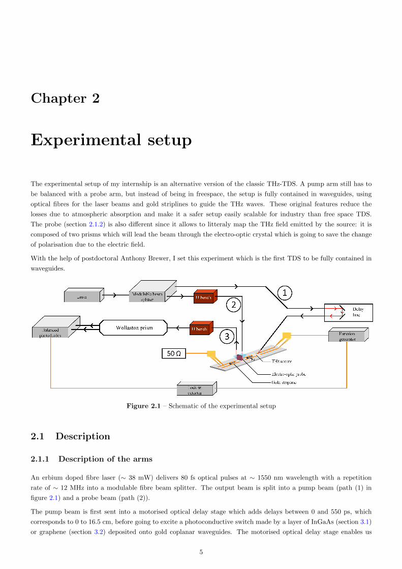
The experimental setup of my internship is an alternative version of the classic THz-TDS. A pump arm still has to
be balanced with a probe arm, but instead of being in freespace, the setup is fully contained in waveguides, using
optical fibres for the laser beams and gold striplines to guide the THz waves. These original features reduce the
losses due to atmospheric absorption and make it a safer setup easily scalable for industry than free space TDS.
The probe (section 2.1.2) is also different since it allows to litteraly map the THz field emitted by the source: it is
composed of two prisms which will lead the beam through the electro-optic crystal which is going to save the change
of polarisation due to the electric field.
With the help of postdoctoral Anthony Brewer, I set this experiment which is the first TDS to be fully contained in
waveguides.
Figure 2.1 – Schematic of the experimental setup
2.1 Description
2.1.1 Description of the arms
An erbium doped fibre laser (∼ 38 mW) delivers 80 fs optical pulses at ∼ 1550 nm wavelength with a repetition
rate of ∼ 12 MHz into a modulable fibre beam splitter. The output beam is split into a pump beam (path (1) in
figure 2.1) and a probe beam (path (2)).
The pump beam is first sent into a motorised optical delay stage which adds delays between 0 and 550 ps, which
corresponds to 0 to 16.5 cm, before going to excite a photoconductive switch made by a layer of InGaAs (section 3.1)
or graphene (section 3.2) deposited onto gold coplanar waveguides. The motorised optical delay stage enables us
5

2.1. DESCRIPTION CHAPTER 2. EXPERIMENTAL SETUP
to explore the entire width of the terahertz pulse by controlling the delay line between the probe beam and the
terahertz wave generated by the photoswitch. Illuminated by the laser pulse with a 50 µm focal length fibre and
biased with a DC voltage of 8 ∼ 11 V, the photoswitch generates THz pulses which can propagate along gold
waveguides (section 1.2.1). The propagating terahertz field is the electric field the electro-optic probe will sense.
The probe beam is sent into a U-bench, which is a free space area where waveplates adapted to optical fibre beams
can be inserted. This allows us to change the polarisation of the pump optical beam. Just like in a regular TDS, the
probe beam is then sent into an electro-optic crystal probe, thanks to two prisms which lead the beam down to the
electro-optic crystal where it gets its polarisation changed if there is any THz electric field, before leading it back up
to the detection arm (path (3) in figure 2.1). A more detailed description of our original electro-optic probe is given
in section 2.1.2.
Another U-bench can be found on the detection arm. Since the optical fibres do not save the polarisation of the
optical beam, this U-bench allows us to change it before we reach the Wollaston prism where the polarisation must
be circular to reach the best signal-to-noise ratio at the balanced photodiodes. Indeed, the Wollaston prism will split
a circular polarisation beam into a vertical and a horizontal polarisation beams and substract one to the other. The
polarisation must be circular to reduce the noise (section 1.2.2). The balanced photodiodes finally sends the data to
the lock-in detector which is synchronised with the Function generator that apply the bias to the photoswitch.
The usual fibre used for this entire setup is the SMF-28, which has a dispersion coefficient of 18 ps(nm · km).
Considering dramatic dispersion effects (section 1.2.3), a fibre with a negative dispersion coefficient has to be used
to preserve a ∼ 100 fs pulse duration. We inserted it at the beginning of the setup, between the laser and the beam
splitter.
Considering the dispersion and the arm balance contraints, multiple fibres were made to limit chromatic dispersive
effects in the optical fibres. We successfully ended up with a 105 fs and a 95 fs pulses respectively for the probe
and the pump beams which are really short pulses considering how a few centimetres can change the pulse duration
(figure 1.2). These pulse lengths were measured thanks to an autocorrelator.
The ends of the fibers were polished to yield a defect free surface under microscopic inspection and fibres were
inspected to be low loss: about 1 dB loss was measured for all the fibres regardless of their lengths, suggesting
the losses come from the connectors. Also, the free space areas U-benches showed losses of 0.8 and 1 dB which
approximatively match the specifications which mentioned 0.6 dB losses.
2.1.2 Electro-optic probe
Figure 2.2 – Schematic of the electro-optic probe
Apart from the optical fibres, the electro-optic probe is probably the most important part of our new setup. It will
allow us to detect guided terahertz waves and make a map of its propagation. A schematic of this electro-optic probe
can be found in figure 2.2.
6

CHAPTER 2. EXPERIMENTAL SETUP 2.2. OPTIMISATION
The electro-optic probe is composed by two fibres leading the laser beam in and out of the probe itself and two
prisms which will lead the beam through the ZnTe electro-optic crystal which is the actual core of the probe. The
fibres and the probe are attached to the same motorised stage which allows controlled 3D motions of the ensemble
by computer. This feature will enable 3D mapping of the terahertz field thanks to LabView. Optical adhesive with
the same refractive index than the prisms’ stick the prisms, the electro-optic crystal and the metallic tip attached to
the stage together.
The fibres used for this electro-optic probe have a lense at their end with a focal length of 500 µm. The laser beam
must be focused on the electro-optic crystal to maximise the signal. Mechanic screws allow independent adjustments
of the position of the fibres and their angle in respect to each other and to the probe to achieve optimal focus. The
power was measured at the collection fibre in order to verify that.
The electro-optic crystal chosen is ZnTe. It has been chosen for its relatively high electro-optic coefficient and
coherence length for 1550 wave lengths: respectively 5.5 pm/V [20] and 0.15 mm [21]. In comparison, GaAs has
respectively 1.5 pm/V and 0.8 mm [21] electro-optic coefficient and coherence length. ZnTe therefore has a shorter
coherence length than GaAs, but considering the thickness of our crystal (200 nm), this short length will not have
any incidence on our experiment. In addition of its three-times-higher electro-optic coefficient, ZnTe also shows a
dieletric permittivity twice as low as GaAs’s (6.7 vs. 13.1 [22]). The terahertz field will therefore be less disturbed
by a ZnTe than a GaAs crystal.
To limit the reflections at the interface prism/crystal, an anti-reflective coating layer SiNH3 (n = 1.91) of thickness
171, 6nm has been added by PECVD to the two faces of the electro-optic crystal.
2.2 Optimisation
As mentioned in section 1.2.3, there are two constraints on the fibres to consider: the balance of the two arms and
the dispersion.
� The arm balance has been achieved thanks to a set of three fibres of different lengths we have prepared in case we
needed to make short time adjustments. Scans with the delay line would tell us if the arms are time-balanced.
� At the same time, the dispersion problem had to be considered: the dispersion equation implies a significant
increase of the pulse duration if we only use positive dispersion coefficient fibres. A negative dispersion fibre
was therefore added at the beginning of the setup. We first made it too long to insure we can still achieve to
find the minimum duration if we shorten it, and shortened it part by part. The pulse duration was checked
after everytime we shortened the fibre with an autocorrelator. When we were finally satisfied with the pulse
duration, the lensed connector of the fibre was glued with epoxy.
� We successfully achieved 95 fs and 105 fs respectively for the pump and the probe beam durations, knowing that
the laser would provide a 80 fs pulse duration and a 1 cm fiber would change the duration of 17 femtoseconds
(figure 1.2).
An important optimisation of the setup was the alignment of the probe and the fibres
� We wanted both the electro-optic crystal and the fibres to be aligned horizontally, so the crystal is aligned to
the sample and the fibres are aligned to the probe. Electro-optic crystal was aligned to the horizontal axis by
using a flat surface and illuminating the probe at the opposit side of where we set a camera. Moving the probe
thanks to the motorised stage, we checked if the distance between the probe and the surface would change and
validate if it was horizontal (figure 2.3).
� With the electro-optic probe out of the way, the fibres were horizontally aligned in respect to a horizontal
mirror and a circulator. A circulator is a 3-fibres device with an input, an output where laser can reflect on a
7

2.2. OPTIMISATION CHAPTER 2. EXPERIMENTAL SETUP
mirror and a second output where the reflection power is measured. We maximised the power at this second
output by changing the angle of the injection and the collection fibres.
� The fibres were then aligned in respect to the prisms to find the most important power with the output beam.
The electro-optic probe was first roughly aligned with the prisms, and we tried to maximise the power by
changing the position and the angle of the fibres. This step was necessary because of the inhomogeneous
surface which was partly covered by optical adhesive, necessary for the probe to stick to the motorised stage.
A powermeter was used to measure the output beam power.
Figure 2.3 – Electro-optic probe alignment
In order to maximise the signal, a last work has to be done on the polarisation. These steps must actually be done
when the signal is found (section 3.1).
� A circular polarisation at the Wollaston prism is required to minimise the noise so a quarter waveplate and
a polariser were put on the U-bench just before. The noise is minimum when the photodiodes are balanced,
namely when there is no offset when the delay line is off the signal.
Several steps of this optimisation have to be repeated before every measurement, especially the alignment of the
fibres when the probe moved and the balance of the photodiodes.
8

Chapter 3
Measurements & Results
3.1 InGaAs photoswitches
This part is dedicated of generating terahertz with InGaAs photoswitches, detecting it and trying to find the highest
signal-to-noise ratio. In order to generate terahertz and optimise the detection, photoswitches must be biased, the
pump fibre must be aligned to the THz source, the probe has to be positioned as close as possible to the emitter so
we can optimise the signal, the polarisation must be controled and fixed, and a scan in X must be performed to find
the optimal position for the electro-optic probe.
The first thing to do, once the pulse duration checked with the autocorrelator, is to insure we detect THz pulses
with known samples. Therefore, we were provided a few chips with some photoswitches and we set them in the
experimental setup such as indicated in figure 3.1.
Figure 3.1 – Schematic of the gold striplines with InGaAs photoswitch
Every photoswitch was made of a gold center stripline on which a voltage was applied and two surrounding gold
striplines which would be the ground. The substrate was InP and the photoswitch was defined by a gap on which
an InGaAs layer was deposited.
9

3.1. INGAAS PHOTOSWITCHES CHAPTER 3. MEASUREMENTS & RESULTS
We have tested several of them, the resistance between the two ends generally sorting out which photoswitches were
working or not. The two photoswitches which gave the best experimental results were 20 µm gap photoswitches. The
length of the striplines is also critical if you want to avoid reflections to disturb the main signal. Unfortunately, the
chips we were provided showed to be only 4 mm only, which would cause reflections to come back under the probe
within 13.3 ps.
3.1.1 Electrical characterisation
For the electrical characterisation, we wanted to know what would be the maximum photocurrent that can be
produced by our sample. In order to find it, the pump fibre has to be aligned to the InGaAs photoswitch layer in
order to show the lowest resistance between the two ends of the gold striplines: indeed, a lower resistance actually
means a higher photocurrent is generated, which is proportionnal to the terahertz wave amplitude. I/V curves were
then taken in order to know what bias could be applied to measure the photocurrent and avoid risking burning the
InGaAs layer:
0 1 2 3 4 5 6 7 8 90
200
400
600
800
1000
1200
1400
1600
1800
2000
I (µA
)
V applied (V)
I light I dark
R(light) = 5.5 kR(dark) = 7.8 k Photocurrent
(a) I/V curves of an 20 µm InGaAs gap photoswitch
0 1 2 3 4 5 6 7 8 90
100
200
300
400
500
600
Ph
otoc
urre
nt (
A)
V applied (V)
Photocurrent
(b) Photocurrent as a function of the bias voltage
Figure 3.2 – I/V curve and photocurrent measurementsI light is the current measured when the photoswitch is illuminated by the pump. I dark is the current measured
when it is not. Photocurrent is measured by substracting I dark to I light.
The photocurrent is an additional current which appears when the sample is excited by the pump laser. This explains
why the current is higher when the sample is illuminated than when it is not. It is an important data since it is the
source term of the terahertz signal.
3.1.2 Delay line measurement
Following step consisted in positioning the electro-optic probe to maximise the signal measured at the photodiodes.
In order to do so, the probe was lowered and positioned as close as possible to the metallic waveguides and to the
InGaAs photoswitch: since the substrate absorbates the THz, we expect the THz wave to be attenuated if the scan
is taken too far from the photoswitch.
Finally, a 8.5 V bias was applied to the photoswitch and, using the delay line, a large bandwidth scan was performed
to find the zero delay between pump and probe beam. One scan result after several tries is shown in figure 3.3.
10

CHAPTER 3. MEASUREMENTS & RESULTS 3.1. INGAAS PHOTOSWITCHES
220 230 240 250 260 270 280 290 300-5
0
5
10
15
20
25
30
Am
plitu
de (
V)
Time (ps)
InGaAs generated THz
(a) InGaAs THz pulse scanning the different delay times
0,0 0,5 1,0 1,5 2,0 2,5 3,00,01
0,1
1
10
Ampl
itude
Frequency (THz)
InGaAs generated THz
(b) FFT of the THz pulse on a logarithmic scale
Figure 3.3 – InGaAs THz pulse obtained by varying the delay line length
We observe a main peak which has an amplitude of 30.4 µV and a FWHM of 2.3 ps. Oscillations which follow are
explained by the fact that gold striplines were very short, causing multiple reflections of the THz wave. Besides,
the noise amplitude is 0.57 µV, which is very low compared with the signal. The FFT of this scan is reported in
figure 3.3b: it shows the bandwidth of the photoswitch which is approximatively 1.1 THz, when the signal becomes
too noisy to be distinguishable.
However, such a result could not have be found immediately. Indeed, the experimental setup is also very sensitive to
the polarisation of the light. Besides, the fibres we use do not save it. Finding the best polarisation to optimise the
signal was therefore a challenge. In practice, finding the circular polarisation means modifying it in order to find the
highest amplitude at the lock-in detector with the delay line positioned at the main peak. In order to perform this
optimisation of the polarisation, we could:
� Twist fibres
� Change the polarisation of the laser source
� Insert waveplates on the U-benches (polarisers, half-wave plates, quarter-wave plates)
By trying to optimise the polarisation using these elements, we could improve the signal-to-noise ratio by optimising
it between the probe and the Wollaston prism and increase the amplitude of the signal by changing the polarisation
on the probe arm.
Once the signal optimised, fibres were stuck to the table, the polarisation of the source was saved and the U-benches
coverted. This significantly improved the amplitude of the signal. The photodiodes could be balanced again at this
stage.
3.1.3 X measurements
A scan in the X direction at a constant delay line length - the optimal length - was performed. The result is shown
in figure 3.4b.
11

3.1. INGAAS PHOTOSWITCHES CHAPTER 3. MEASUREMENTS & RESULTS
(a) Schematic of the direction scanned from the side
-0,6 -0,4 -0,2 0,0 0,2 0,4 0,6
-10
0
10
20
30
Ampl
itude
(A)
X (mm)
InGaAs THz
(b) X scan result of the InGaAs gap photoswitch
Figure 3.4 – X scan of the InGaAs photoswitch
We find a very clear trace with a positive and a negative peak. A fundamental information is deduced from it: indeed,
since the electro-optic probe was made in the laboratory and we did not have a way to know the orientation of the
electro-optic crystal at this time, it could have two possible orientations making it sensitive to either horizontal or
vertical THz field components (figure 3.5).
(a) Horizontal sensitivity (b) Vertical sensitivity
Figure 3.5 – Horizontal sensitivity vs. vertical sensitivity of the electro-optic crystal
From these schematics indicating the sign and the amplitude of the THz electric field we are supposed to find
depending on the sensitivity of the probe and our results of the X-scan (figure 3.4b), we can clearly state that our
probe is sensitive to the horizontal component of the THz electric field.
3.1.4 Signal-to-noise ratio
After optimising the pump position, the polarisation and the X-position of the probe, we finally got interested in the
signal-to-noise ratio:
� The signal amplitude at the lock-in was up to 45 µV.
� The noise amplitude was 0.57 µV.
� The signal-to-noise ratio was therefore 78.9.
Considering that the photocurrent was 525.8 ± 5µA, we finally calculated the potential signal-to-noise ratio as a
function of the photocurrent for our InGaAs samples.
12

CHAPTER 3. MEASUREMENTS & RESULTS 3.2. GRAPHENE PHOTOSWITCHES
0 100 200 300 400 5000
10
20
30
40
50
60
70
80
Pote
ntia
l sig
nal-t
o-no
ise
ratio
Photocurrent ( A)
Figure 3.6 – Potential signal-to-noise ratio as a function of the photocurrent
This figure will unfortunately not apply directly to our graphene photoswitches because the physics origins of the
THz generation are different and the shape of the photocurrent pulses will therefore be different. However, it gives
an estimation of the minimum average photocurrent our system is able to detect.
3.2 Graphene photoswitches
Our graphene samples are the core of my internship, since I spent about one quarter of my time in a clean room
to produce them. The closest related work has been realised by Prechtel & al. [23] in January 2012, where the
researchers showed THz pulses with a precision of the order of magnitude of a picosecond, when we will have a
precision of a tens of femtoseconds.
3.2.1 Description
Figure 3.7 – Schematic of our graphene-based photoswichesTwo types of samples were fabricated. The only difference between the two of them was the presence of the
graphene probed layer
In order to make our measurements, two kinds of samples were produced (figure 3.7):
13

3.2. GRAPHENE PHOTOSWITCHES CHAPTER 3. MEASUREMENTS & RESULTS
� One set of photoswitches was made without the graphene to be probed layer. It was made to investigate
the possibility for graphene excited by femtosecond optical pulses to deliver THz radiation and analyse its
propagation.
� Another set of photoswitches was produced to analyse the permittivity of a graphene layer in the THz range:
a terahertz pulse is produced by one layer of graphene excited by the pulse laser and then propagates along the
striplines until it reaches the second layer of graphene where the THz signal is scanned.
In both cases, a graphene layer coupled with two gold layers separated by a gap define a photoswitch. This photoswitch
should produce a terahertz wave that propagates along the gold striplines which additionally play a role of waveguides
keeping the terahertz confined in two dimensions. The gold striplines stick to the Topas® thanks to a 10 nm Ti
layer between them. The fabrication of these samples is detailed in section 3.2.3. Notice that the Al layer and Si
layer from figure 3.7 planned to be removed for the terahertz measurement, to only leave Topas® as a substrate.
Topas® is a thermoplastic which is very flexible regarding the glass transition temperature: it can indeed be modified
between 70°C and 170°C by changing the relative concentration norbornene from which it is synthetised (figure 3.8)
[24]. In addition to this remarkable property, Topas® has been chosen as a substrate for our experiment because of
its very low absorption in the terahertz bandwidth [25]. This will allow us to limit absorption of THz waves when they
will propagate along the gold waveguides. A counterpart of Topas® is its tendency to produce air bubbles during
the fabrication, either because of acetone attacking the material at the edges, either because of its melting during
the photolithography process during which it is repeatedly heated. This property increased the failure rate of our
photoswitch production.
Figure 3.8 – Topas® molecule
Illuminating graphene with femtosecond opical pulses can provide efficient THz pulse generation since it has a very
high electron mobility. It will also provide richful information on physical mechanisms in graphene.
3.2.2 Graphene growth and characterisation
Figure 3.9 – Graphene growth by CVD
14
CHAPTER 3. MEASUREMENTS & RESULTS 3.2. GRAPHENE PHOTOSWITCHES
Graphene was grown by Chemical Vapor Deposition at Laboratoire Pierre Aigrain (figure 3.9). A known program
was applied to grow single layer graphene on copper substrate:
� Pressure is decreased until 0.1 mbar. The low pressure helps to prevent unwanted reactions and produce more
uniform thickness of coating on the substrate.
� CH4 is sent inside the box. These are the carbon atom providers which are necessary to produce graphene.
� Temperature is increased up to 775K to break the CH4 molecules.
� Argon is sent inside as a neutral gas to increase the gas flow without adding more carbon atoms.
� Hydrogen is sent during the heating to clean the sample.
� Temperature cools down to room temperature and pressure to atmospheric pressure.
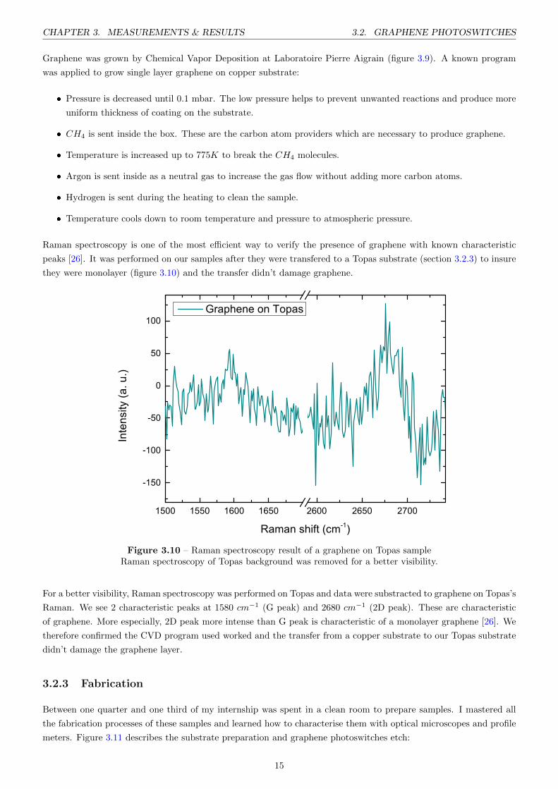
Raman spectroscopy is one of the most efficient way to verify the presence of graphene with known characteristic
peaks [26]. It was performed on our samples after they were transfered to a Topas substrate (section 3.2.3) to insure
they were monolayer (figure 3.10) and the transfer didn’t damage graphene.
1500 1550 1600 1650 2600 2650 2700
-150
-100
-50
0
50
100
Inte
nsity
(a. u
.)
Raman shift (cm-1)
Graphene on Topas
Figure 3.10 – Raman spectroscopy result of a graphene on Topas sampleRaman spectroscopy of Topas background was removed for a better visibility.
For a better visibility, Raman spectroscopy was performed on Topas and data were substracted to graphene on Topas’s
Raman. We see 2 characteristic peaks at 1580 cm−1 (G peak) and 2680 cm−1 (2D peak). These are characteristic
of graphene. More especially, 2D peak more intense than G peak is characteristic of a monolayer graphene [26]. We
therefore confirmed the CVD program used worked and the transfer from a copper substrate to our Topas substrate
didn’t damage the graphene layer.
3.2.3 Fabrication
Between one quarter and one third of my internship was spent in a clean room to prepare samples. I mastered all
the fabrication processes of these samples and learned how to characterise them with optical microscopes and profile
meters. Figure 3.11 describes the substrate preparation and graphene photoswitches etch:
15

3.2. GRAPHENE PHOTOSWITCHES CHAPTER 3. MEASUREMENTS & RESULTS
Figure 3.11 – Fabrication of photoswitches (1/2)
Once the graphene is defined, the following step consists on depositing gold striplines by photolithography and
electron beam evaporation:
Figure 3.12 – Fabrication of photoswitches (2/2)
16
CHAPTER 3. MEASUREMENTS & RESULTS 3.2. GRAPHENE PHOTOSWITCHES
3.2.4 Electric characterisation
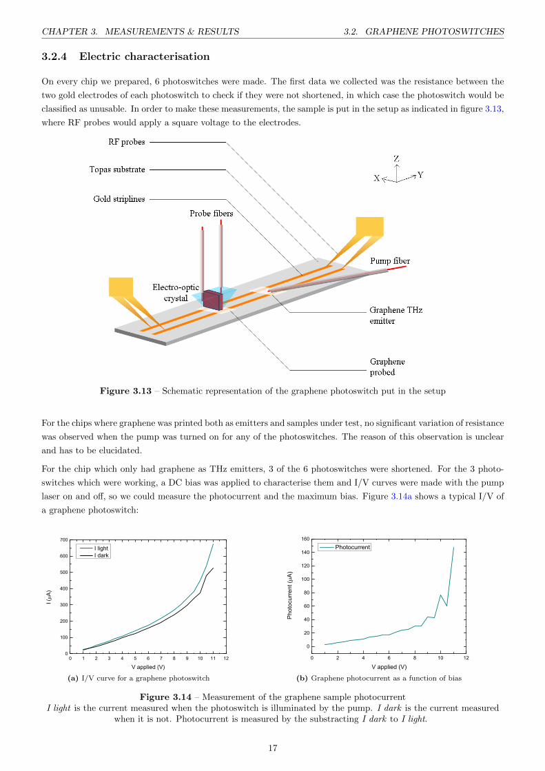
On every chip we prepared, 6 photoswitches were made. The first data we collected was the resistance between the
two gold electrodes of each photoswitch to check if they were not shortened, in which case the photoswitch would be
classified as unusable. In order to make these measurements, the sample is put in the setup as indicated in figure 3.13,
where RF probes would apply a square voltage to the electrodes.
Figure 3.13 – Schematic representation of the graphene photoswitch put in the setup
For the chips where graphene was printed both as emitters and samples under test, no significant variation of resistance
was observed when the pump was turned on for any of the photoswitches. The reason of this observation is unclear
and has to be elucidated.
For the chip which only had graphene as THz emitters, 3 of the 6 photoswitches were shortened. For the 3 photo-
switches which were working, a DC bias was applied to characterise them and I/V curves were made with the pump
laser on and off, so we could measure the photocurrent and the maximum bias. Figure 3.14a shows a typical I/V of
a graphene photoswitch:
0 1 2 3 4 5 6 7 8 9 10 11 120
100
200
300
400
500
600
700
I (A)
V applied (V)
I light I dark
(a) I/V curve for a graphene photoswitch
0 2 4 6 8 10 12
0
20
40
60
80
100
120
140
160
Phot
ocur
rent
(A)
V applied (V)
Photocurrent
(b) Graphene photocurrent as a function of bias
Figure 3.14 – Measurement of the graphene sample photocurrentI light is the current measured when the photoswitch is illuminated by the pump. I dark is the current measured
when it is not. Photocurrent is measured by the substracting I dark to I light.
17

3.3. EXPECTATIONS CHAPTER 3. MEASUREMENTS & RESULTS
From these I/V curves, photocurrent can be deduced by substracting I dark to I light. No article before showed any
I/V describing photocurrent generated by graphene illuminated by femtosecond optical pulses.
Because of Joule heating, graphene could easily burn when it was excited by the high power laser and when a bias
was applied to the photoswitch. We characterised all the photoswitches of the first chip in order to find the maximum
bias that could be applied to them:
Photoswitch number Breaking bias Photocurrent measured
1 8.46 ± 0.38kV.cm−1 148 ± 1µA2 8.46 ± 0.38kV.cm−1 54 ± 1µA3 8.46 ± 0.38kV.cm−1 19 ± 1µA
Table 3.1 – Photoswitch breaking bias and their respective photocurrent
The variation of the surface state quality due to the Topas® during the sample fabrication mainly explains the
difference of maximum photocurrent measured. Dust depositing during the long fabrication process can also explain
a few differences but in any case, since photocurrent is few tens of µA, we believe all of these samples would have
allowed us to detect the terahertz signal.
3.3 Expectations
At the time I am finishing this report, we are aligning the setup again with our new samples. These samples show
lower photocurrent (up to 15 µA), but we still believe we will be able to detect a terahertz wave.
The plan for this measurement is to align the fibres in respect of the electro-optic probe. Then, a 9 V bias with an
AC generator will be applied to insure the safety of graphene, and two scans will be performed at the same delay
line than for the InGaAs scans (figure 3.3a):
� A scan with the delay line varying. We expect the same result than figure 3.3a with a lower amplitude and
fewer oscillations after the main peak, because we made longer striplines than the ones we had on the InGaAs
samples.
� A scan with a LabView script at the optimal delay line, scanning with X and Z. This will show us how the
terahertz field attenuates in Z.
For an X scan, taking into account the fact that we now only have one ground stripline (to oppose to the two ground
striplines in section 3.1.3), we would expect only one positive peak (or negative peak depending on the bias) with
our probe:
(a) Schematic of the THz field for an X scan
-0,6 -0,4 -0,2 0,0 0,2 0,4 0,6
0
5
10
15
20
25
30
35
Ampl
itude
(µA)
X (mm)
Graphene THz expectations
(b) X scan expectations for our graphene photoswitch
Figure 3.15 – Result expectations for our graphene photoswitch
18

Conclusion and perspectives
During this four-month internship, I have been involved in every step of an experiment: we have been able to build
a new fully-waveguided setup based on the previous work of Dr. Djamal Gacemi, I participated to the sample
fabrication using CVD, in clean rooms with several processes to define the waveguides, characterised these samples
optically, electrically and with Raman spectroscopy. I calibrated and optimised our setup, made the measurements,
processed the data and verified that THz waves generated were indeed confined.
In order to prepare the experiment, I had to make optical fibres at a very accurate precision, to align fibres according
to the new electro-optic probe and to use optical waveplates in order to have a circularly-polarised signal right before
the detection and maximise the terahertz signal. A large part of my internship also included sample preparation in a
clean room, where I repeatedly used the photolithography, the Electron-Beam Evaporator, the Reactive Ion Etching
(RIE) machine and Plasma-Enhanced Chemical Vapor Deposition (PECVD).
This setup I have been working on is very promising in many aspects: first, the fact that it is fully contained in optical
fibres considerably reduce the losses for a spectroscopy setup. Another direct consequence of the use of optical fibres
is the scalability by industry. Therefore, one could imagine a next version of our setup where you just introduce a
new material to test, and everything is automatised. This may be the first prototype of a compact THz-TDS which
enables the probing of small objects in the THz range.
The InGaAs photoswitches we tested gave results we expected, since Djamal Gacemi tested them before us, but we
successfully detected photocurrent with our new graphene-based samples and are quite confident we are going to
detect a THz signal in the next few days. Such a THz emission was only measured by one team before [23], but it
was achieved with freely suspended graphene and they have not tried to explain the origins of the emission. Also, we
will be able to add a propagation map of the THz field and we hope, by increasing the amplitude of the THz pulses,
we will be able to map the absorption of the THz field by any 2D sample. This unfortunately haven’t been possible
due to the absence of photocurrent detected when we added a graphene probe sample on the waveguides.
Many improvements can still be done on our experiment: industrialisation has already been mentioned. It can
improve the quality of our fibres - and therefore reduce the losses - and much more accurate cuts can be done to
shorten the pulses. Our probe would particularly benefit an industrial fabrication to flatten the surface (currently
and necessarily coverted with optical adhesive) and balance the prisms, and the control of the polarisation could be
optimised. Multi-layer graphene can be tested to generate THz and we still need a script to synchronise the motion
of the delay line with the electro-optic probe to be able to make a 3D map of the THz field propagation.
19

Software credit
� Composition: LYX 2.0 / WinEdt 8
� Schematics: Adobe Fireworks CS6
� Molecules: Accelrys Draw 4.1
� Spectra / Data processing: OriginPro 9.0
ix

Bibliography
[1] P. L. Stiles, J. A. Dieringer, N. C. Shah, R. P. Van Duyne, Surface-enhanced raman spectroscopy, Annual Review
of Analatycal Chemistry, 1: 601-626, 2008.
[2] W. L. Barnes, A. Dereux, T. W. Ebbesen et al, Surface plasmon subwavelength optics, Nature, 424 (6950):
824-830, August 2003.
[3] D. K. Gramotnev, S. I. Bozhevolnyi, Plasmonics beyond the diffraction limit, Nature Photonics, 4 (2): 83-91,
2010.
[4] S. Kawata, Y. Inouye, P. Verma, Plasmonics for near-field nano-imaging and superlensing, Nature Photonics, 3
(7): 388-394, 2009.
[5] J. N. Anker, W. P. Hall, O. Lyandres, N. C. Shah, J. Zhao, R. P. Van Duyne. Biosensing with plasmonic
nanosensors, Nature materials, 7 (6): 442-453, 2008.
[6] J. Homola et al, Surface plasmon resonance sensors for detection of chemical and biological species, Chemical
reviews, 108 (2): 462, 2008.
[7] T.W. Ebbesen, C. Genet, S.I. Bozhevolnyi, Surface-plasmon circuitry, Physics Today, 61 (5): 44, 2008.
[8] J. Zenneck, Les oscillations electromagnetiques et la telegraphie sans fil, Volume 2, Gauthier-Villars, 1908.
[9] G. Goubau, Surface waves and their application to transmission lines, Journal of Applied Physics, Vol 21:
1119-1128 (1950).
[10] C. R. Williams, S. R. Andrews, S. A. Maier, A. I. Fernandez-Dominguez, L. Martin-Moreno, F. J. Garcia-Vidal,
Highly conned guiding of terahertz surface plasmon polaritons on structured metal surfaces, Nature Photonics, 2
(3): 175-179, 2008.
[11] R. Mendis, D. Grischkowsky, Undistorted guided-wave propagation of subpicosecond terahertz pulses, Optics
letters, 26 (11): 846-848, 2001.
[12] D. E. Gacemi, Etudes experimentale et simulation des modes electromagnetiques se propageant sur des guides
d’ondes metalliques de petites dimensions aux frequences THz, Thesis, December 2012.
[13] D. E. Gacemi, J. Mangeney, R. Colombelli, A. Degiron, Subwavelength metallic waveguides as a tool for extreme
confinement of THz surface waves, March 2013.
[14] D. E. Gacemi, A. Degiron, M. Baillergeau, J. Mangeney, Identification of several propagation regimes for terahertz
surface waves guided by planar Goubau lines, October 2013.
[15] Y. Kawano, K. Ishibashi, An on-chip near-field terahertz probe and detector, Nature Photonics, 2 (10): 618-621,
2008.
[16] J. Liu, R. Mendis, D. M. Mittleman, N. Sakoda, A tapered parallel-plate-waveguide probe for THz near-field
reflection imaging, Applied Physics Letters, 100 (3): 031101, 2012.
x

BIBLIOGRAPHY BIBLIOGRAPHY
[17] M. Nagel, P. H. Bolivar, M. Brucherseifer, H. Kurz, A. Bosserho, R. Buttner, Integrated THz technology for
label-free genetic diagnostics, Applied Physics Letters, 80: 154, 2002.
[18] P. C. Upadhya et al., Excitation-density-dependent generation of broadband terahertz radiation in an asymmet-
rically excited photoconductive antenna, Optics Letters, vol. 32, no. 16, pp. 2297-2299, 2007.
[19] M. Ashida, Ultra-Broadband Terahertz Wave Detection Using Photoconductive Antenna, Japanese Journal of
Applied Physics, vol. 47, 8221, 2008.
[20] Y. Jeon, H.S. Kang, Electro-optic coefficient measurements for ZnxCd1−xTe single crystals at 1550 nm Wave-
length, Optical review, Vol 14 (6) 373-375, 2007.
[21] M. Nagai, K. Tanaka, H. Ohtake, T. Bessho, T. Sugiura, T. Hirosumi, M. Yoshida, Generation and detection of
terahertz radiation by electro-optical process in GaAs using 1.56 µm fiber laser pulses, Applied Physics Letters,
Vol. 85 (18) 3974-3976, 2004.
[22] S. Casalbuoni, H. Schlarb, B. Schmidt, P. Schmuser, B. Steffen, A. Winter, Numerical Studies of the Electro-
Optic Sampling of Relativistic Electron Bunches, TESLA Report, January 2005.
[23] L. Prechtel, L. Song, D. Schuh, P. Ajayan, W. Wegscheider, A. W. Holleitner, Time-resolved ultrafast photocur-
rents and terahertz generation in freely suspended graphene, Nature Communications, January 2012.
[24] Dan M. Johansen, Investigation of Topas® for use in optical components (Thesis), September 2005.
[25] P. D. Cunningham, N. N. Valdes, F. A. Vallejo, L. M. Hayden, B. Polishak, X.-H. Zhou, J. Luo, A. K.-Y. Jen,
J. C. Williams, R. J. Twieg, Broadband terahertz characterization of the refractive index and absorption of some
important polymeric and organic electro-optic materials, Journal of Applied Physics, Vol. 109 (4), 2011.
[26] A. C. Ferrari, D. M. Barko, Raman spectroscopy as a versatile tool for studying the properties of graphene, Nature
Nanotechnology, Vol. 8, pp. 235-246, April 2013.
xi