manual de usuario bedienungsanleitung manuel dÕutilisation ...v2).pdf · necessarily adds a lot of...
TRANSCRIPT

Owner’s Manual
Manuel d’utilisation
Bedienungsanleitung
Manual de Usuario
2S JGFE
AD30VT modification for FX insert and return
signal
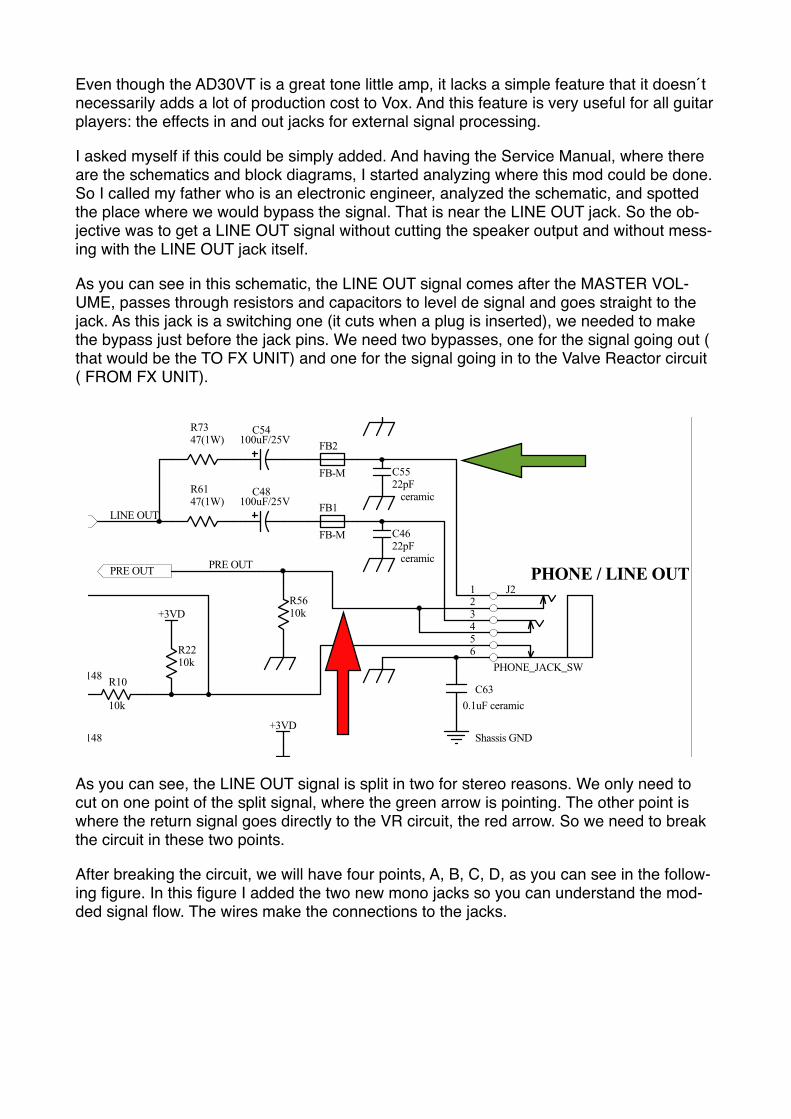
Even though the AD30VT is a great tone little amp, it lacks a simple feature that it doesn´t necessarily adds a lot of production cost to Vox. And this feature is very useful for all guitar players: the effects in and out jacks for external signal processing.
I asked myself if this could be simply added. And having the Service Manual, where there are the schematics and block diagrams, I started analyzing where this mod could be done. So I called my father who is an electronic engineer, analyzed the schematic, and spotted the place where we would bypass the signal. That is near the LINE OUT jack. So the ob-jective was to get a LINE OUT signal without cutting the speaker output and without mess-ing with the LINE OUT jack itself.
As you can see in this schematic, the LINE OUT signal comes after the MASTER VOL-UME, passes through resistors and capacitors to level de signal and goes straight to the jack. As this jack is a switching one (it cuts when a plug is inserted), we needed to make the bypass just before the jack pins. We need two bypasses, one for the signal going out ( that would be the TO FX UNIT) and one for the signal going in to the Valve Reactor circuit ( FROM FX UNIT).
As you can see, the LINE OUT signal is split in two for stereo reasons. We only need to cut on one point of the split signal, where the green arrow is pointing. The other point is where the return signal goes directly to the VR circuit, the red arrow. So we need to break the circuit in these two points.
After breaking the circuit, we will have four points, A, B, C, D, as you can see in the follow-ing figure. In this figure I added the two new mono jacks so you can understand the mod-ded signal flow. The wires make the connections to the jacks.
1 2 3 4 5 6 7 8
A
B
C
D
87654321
D
C
B
A
Q1KTC3198GR
Q2KTC3198GR
SP18ohm
C1100uF/35V
C3247uF/25V
C9
1uF/50V
C11
NU
+15V
C350.22uF
C2622uF/35V
C2722uF/35V
C29
220uF/35V
C30
220uF/35V
+Vcc(+30V)
-Vss(-30V)
C43
10uF/25V
+15V
C42
10uF/25V-15V
C16
0.1uF
C17
0.1uF
Q3KTC3198
A/AB
C31
10uF/16V
C8
1uF/50V
C10
1uF/50V
Max
Max
Min
Min
2
3 4 51
BK
BG
BP
9B
H
AH
CH
V1A12AX7
7
8
6
AG
AP
AK V1B
12AX7
-15V
-15V
-15V
-15V
-15V
+15V
Q4KTA1266
12
3
4
8
IC2ANJM2082D
5
67
IC2BNJM2082D
12
3
4
8
IC3ANJM2082D
5
67
IC3BNJM2082D
R14
2.2k
+3VD
R9
22k
R4047k
-15V
+3VD
R2210k
R10
10k
C410.01uF
PHONE / LINE OUT123456
J2
PHONE_JACK_SW
C120.001uF
C1347pF
R19
470k
R30
68k
R21k
C30.1uF
KLM-2464 1.61
VOX
AGNDDGND
J1
PHONE_JACK STEREO
FOOT SW
R6910k
C500.1uF
HEATER1HEATER2
2004.2.6
9
10 11
IN3
D3 S3
IC1CDG211
IN1
D1 S1
1
2 3
IC1ADG211
16
15 14
IN2
D2 S2
IC1BDG211
8
76
IN4
D4S4
IC1DDG211
1 1
2 2
3 3
4 4
5 5
6 6
7 7
8 8
9 9
CN1
EH-9
RES_FRQ
POWER LEVEL
0 : ON1 : OFF
0 : ON1 : OFF
0 : ON1 : OFF
0 : ON1 : OFF
V+
V-
GND
13
5
4
12
DG211
IC1
C150.1uF
C14
0.1uF
R722k
-15V
+15V
C60.1uF
C50.1uF
11
22
CN2
VH-210 INCH
R11k
R54.7k
R64.7k
R38
47k
R3
4.7k
R3933k R4
4.7k
R20
220
R23
47k R2433k
R27
47k R2833k
R26
2.2k R810k
R41330
R425.6k
R32
330k
R31
330k
R33
330k
R34
330k
R35
3.3k
R36
3.3k
R434.7k
R15
2.2k
R18
2.2k
R17
2.2k
R48
0.47(3W)
R4610 (1W)
+3VD
3
2
1
VR1A100kB
3
2
1
VR1B100kB
R21
220
R2510k
R441.8k
R452.2k
R29 22k
+
C34 NU
+ C3347uF/35V
Title
Size Number Revision
Date Sheet of2/2
A2
AD30VT POWER PCB
+3VD
3
1
2D1KBP206G
3
4
5
C36
2200uF/50V
C37
2200uF/50V
C180.1uF
C190.1uF
1 3
2
V V
GNDIN OUT
IC57815
C200.1uF
C210.1uF
C220.1uF
C230.1uF
D21N4002
D51N4002
C38100uF/25V
C39100uF/25V
4
D7SHSW04M
6
7
C452200uF/16V
1 3
2
V V
GNDIN OUT
IC7BA033T
C240.1uF
C250.1uF
D61N4002
C40100uF/6.3V
5
8
9
HEATER1
HEATER2
1
10
2
R49
330(1W)
R50
330(1W)
R51
100(1W)
R52
100(1W)
1 2
SW1SW-SPST
F1
FUSE
F2
FUSE
1
OUT 3IN2GND
IC67915
R54470
LED1RED(5mm)
11
22
33
CN4
EH-3
1 1
2 2
3 3
CN5
EH-3
POWER
POWER 11
22
33
44
55
66
77
88
CN3
EH-8
R47 10 (1W)
C44 0.22uF
D4 1N4002
D3 1N4002
Chassis GND Circuit GND
Chassis GND
NC FOOT_ SW_R
+VCC(+30V)
-VSS(-30V)-15V
+15V
+3VD
R55
0
AGND
DGND
NC : No Connect
D141N4148
D151N4148
D81N4148
D91N4148
FB1
FB-M C4622pF
LINE OUT
PRE OUT
PHONE_DT
PHONE_DT
LINE OUT
PRE OUT
FOOT_SW_LFOOT_SW_L
PHONE_DT
LINE OUT
PRE OUT
LINE OUT
PRE OUT
PHONE_DT
FOOT_ SW_R
R5610k
HEATER1
HEATER2
HEATER1HEATER2
From MAIN PCB
To MAIN PCB
Q5KTC2874
R57
1k
C47 NU
R58470
R591k
POWER SUPPLY BLOCK
POWER BLOCK
C48100uF/25V
R6147(1W)
Q7KTA1266
Q6KTC3198
R6010k
+3VD
R37100k
R5310k
D121N4002
D131N4002
C490.22uF/50V
Q8
KTC3198
R64
22k R6222k
R65
10k
+3VD
Q9KTC3198
R632.2k
R6716k
0 : A1 : AB
VL
+3VD
R7047k
C53
47uF/35V
-15V
+15V
C2810uF/35V
R66220k
R683.3k
ADJUSTMENT RESISTOR
R1110k
C70.1uF
+3VD
D101N4148
D111N4148
FOOT_SW_L FOOT_SW_L
FOOT_SW_RFOOT_SW_R
FB2
FB-M C5522pF
C54100uF/25V
R7347(1W)
-15V
C24.7uF/50V
C410uF/16V
C56
10uF/16V
3
14
10
9
7
8
IC4 LM3886
R1222k
C630.1uF ceramic
C640.1uF ceramic
Shassis GND
Shassis GND
C570.1uF
C580.1uF
C590.1uF
C600.1uF
C610.1uF
C620.1uF
Shassis GND
Shassis GND
Shassis GND
Shassis GND
ceramic ceramic ceramic ceramic
ceramic ceramic
ceramic
ceramic
ceramic
ceramicceramic
ceramic
ceramic ceramic
ceramic
ceramic
ceramic
ceramic
ceramic
ceramic
ceramic
ceramic
ceramic
ceramic
ceramic
ceramic
ceramic
ceramic
C65NU
C51
3pF ceramic
NU : No Use
R16
0
R130
1,5
C520.1uF
C6610pF
ceramic
ceramic
C67
3.3uF/50V
C68
3.3uF/50V
Vishay Siliconix
R71 47k_F(1%)
R72
47k_F(1%)
(Delete=6dB up)
If the output power is not high enough, please delete both R67 and R68.
Even doing above modify, if the output power is not go to correct level, please exchange the TUBE itself.
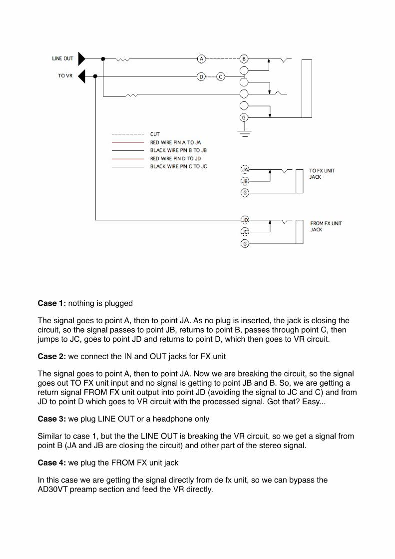
Case 1: nothing is plugged
The signal goes to point A, then to point JA. As no plug is inserted, the jack is closing the circuit, so the signal passes to point JB, returns to point B, passes through point C, then jumps to JC, goes to point JD and returns to point D, which then goes to VR circuit.
Case 2: we connect the IN and OUT jacks for FX unit
The signal goes to point A, then to point JA. Now we are breaking the circuit, so the signal goes out TO FX unit input and no signal is getting to point JB and B. So, we are getting a return signal FROM FX unit output into point JD (avoiding the signal to JC and C) and from JD to point D which goes to VR circuit with the processed signal. Got that? Easy...
Case 3: we plug LINE OUT or a headphone only
Similar to case 1, but the the LINE OUT is breaking the VR circuit, so we get a signal from point B (JA and JB are closing the circuit) and other part of the stereo signal.
Case 4: we plug the FROM FX unit jack
In this case we are getting the signal directly from de fx unit, so we can bypass the AD30VT preamp section and feed the VR directly.
So, to end the theory, four possible scenarios are taken into account with just breaking the circuit at two points.
MATERIALS NEEDED
Ok, all we need is the following:
• 2 mono 1/4 phone switch jacks
• 4 shielded cables (I got them from old headphones)
• Cutter
• Tin
• Solder iron. Drill.
• A bench or desk with good lighting
PROCEDURE
Note 1: If you are unsure of this, just don´t do it! If you know someone with a background in electronic/electric engineer or technician, ask him if he can do it for you. If you feel sure about this, let´s go on with the steps!
Note 2: Obviously, I am not responsible for whatever happens to you and your amp. Take this procedure at your own risk.
1. Unplug all cables and unscrew all screws. First the ones on the back then the ones on the sides.
2. Remove the back panel and unplug the speaker cables. Remember or mark their insert positions.
3. Remove the amp chassis.
4. Remove screws from the bottom of the chassis. There are four plated ones and two black ones (that hold the black heat sink).
5. Remove the nuts from the LINE OUT and FOOT SW jacks. Remove de AMP LEVEL knob and nut.
6. Cut the plastic tie that holds the transformer colored wires with a bunch of white wires that go into the main PCB.
7. Carefully pull out the PCB while holding the heat sink in place (because it is screwed to the LM3886 amp chip) and turn it so that you can see the green side of the PCB. Be-careful with the tube not to touch the top PCB.
8. Locate the LINE OUT jack pins. See photo:

9. With a sharp cutter, cut between the labeled points A-B and C-D. In the photo these are marked in blue. You need to cut enough to break the PCB copper path.
A
BCUT
G
CUT
DG
C

10.Once cut, test connectivity with a tester, between points A-B and C-D to see if you did a good cut.
11.Get four shielded cables. I used them from a headphone cable and got one cable with a red wire plus the shield and a black wire with the shield. So you will end having one pair red/shield and one pair black/shield (or whatever other color). Twist the ends of the wires and “paint” them with tin with a well heated solder iron.
12.Solder the red wires to the tip of each of the mono phone jacks. These are points JA and JD in the schematic. Solder the shields to the ground tip. Next, solder the black wires to the switch of each of the mono phone jacks. These are the points JB and JC.
13.Ok, get one of the jacks and label it TO FX. Then solder the red wire end to pin A (it is easier to use the adjacent upper pin on that same copper path) on the PCB. Then sol-der the shield wire to point G (ground). Next, solder the black wire to pin B and the shield wire to point G.Get the other jack and label it FROM FX. Then solder the red wire end to pin D on the PCB. Then solder the shield wire to point G (above D). Next, solder the black wire to pin C and the shield wire to point G. See photo:

14.Test connectivity with a tester between point A-B and C-D. As the circuit is closed, there should be connectivity.
15.Plug in guitar cables to both TO FX and FROM FX jacks to see it there is connectivity. When we plug we are bypassing so there shouldn´t be connectivity.
16. If everything is OK, you can run a real test to see if it works. Just put the PCB back into the chassis. Only screw the heat sink. Put the chassis in the box but the other way round. Plug speaker cables and power cord. Turn on the amp and see if it is OK. If there is no fire is because everything is OK!! Plug your FX unit to the TO FX jack and FROM FX jack on the amp. Now the signal should be going to your FX unit without cut-ting the speaker! Test it!
17. If everything is OK, unplug everything and pull out the chassis again. Screw the plated screws back to the chassis again.
18.Now you need to drill 2 holes on the chassis for the new jacks. See photo! Make them apart enough so the jacks don´t overlap ( I wasn´t careful enough! I recommend drilling both on the vertical line of the LINE OUT jack). Blow away any metal and plastic parti-cles after you drill de holes. Mount the jacks.
Red Wire
Black WireShield Wire
Red Wire
Black Wire
Shield Wire

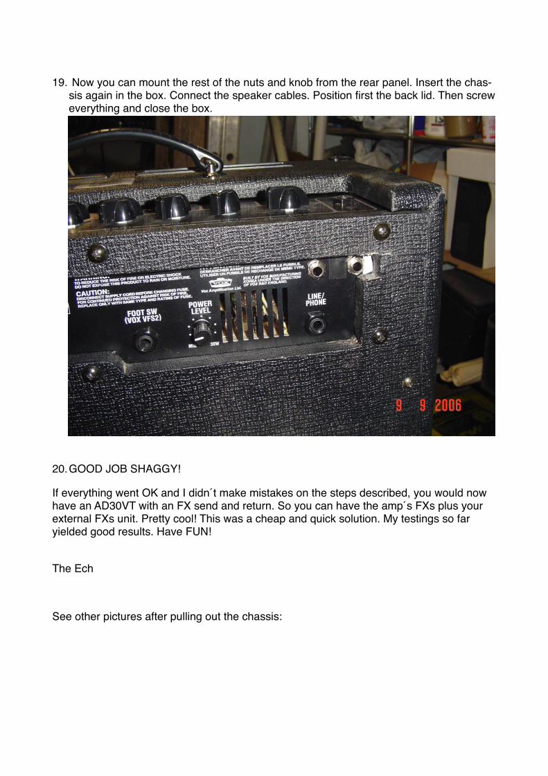
19. Now you can mount the rest of the nuts and knob from the rear panel. Insert the chas-sis again in the box. Connect the speaker cables. Position first the back lid. Then screw everything and close the box.
20.GOOD JOB SHAGGY!
If everything went OK and I didn´t make mistakes on the steps described, you would now have an AD30VT with an FX send and return. So you can have the amp´s FXs plus your external FXs unit. Pretty cool! This was a cheap and quick solution. My testings so far yielded good results. Have FUN!
The Ech
See other pictures after pulling out the chassis:
