manufacturing design and fabrication of 100 nm (leff) cmos
TRANSCRIPT

Rochester Institute of Technology Rochester Institute of Technology
RIT Scholar Works RIT Scholar Works
Theses
6-2014
Manufacturing Design and Fabrication of 100 nm (Leff) CMOS Manufacturing Design and Fabrication of 100 nm (Leff) CMOS
Devices Devices
Samarth Parikh
Follow this and additional works at: https://scholarworks.rit.edu/theses
Recommended Citation Recommended Citation Parikh, Samarth, "Manufacturing Design and Fabrication of 100 nm (Leff) CMOS Devices" (2014). Thesis. Rochester Institute of Technology. Accessed from
This Thesis is brought to you for free and open access by RIT Scholar Works. It has been accepted for inclusion in Theses by an authorized administrator of RIT Scholar Works. For more information, please contact [email protected].

i
Manufacturing Design and Fabrication of 100 nm (Leff) CMOS Devices
by
Samarth Parikh
A Thesis Submitted
in
Partial Fulfillment
of the
Requirements for the Degree of
MASTER OF SCIENCE
in
Microelectronic Engineering
Approved by:
Professor Dr. Lynn F. Fuller (Thesis Advisor) Professor Dr. Robert E. Pearson (Director, Microelectronic Engineering and Thesis Committee Member) Professor Dr. Ivan Puchades (Thesis Committee Member) Professor
Dr. Sohail Dianat (Chair, Electrical end Microelectronic Engineering Department)
DEPARTMENT OF ELECTRICAL AND MICROELECTRONIC ENGINEERING
KATE GLEASON COLLEGE OF ENGINEERING
ROCHESTER INSTITUTE OF TECHNOLOGY
ROCHESTER, NEW YORK
JUNE, 2014

ii
Manufacturing Design and Fabrication of 100 nm (Leff) CMOS Devices
by
Samarth Parikh I, Samarth K. Parikh, hereby grant permission to the Wallace Library, of Rochester Institute of Technology, to produce this document in whole or in part, with the knowledge that any reproduction will not be for commercial use or profit. Samarth K. Parikh Date

iii
I dedicate this master’s thesis to my family- Kaushik, Shilpa, Devarth, Pravin, Minaxi and
Urmil, who have been a constant source of motivation and support to me.

iv
Acknowledgments I would like to express my sincere thanks to Dr. Lynn F. Fuller for believing in me and giving me the opportunity to work on this interesting project. I have learned a great deal from the Microelectronic Manufacturing (CMOS Factory) courses and have thoroughly enjoyed all the three courses that I have taken with you during two years of my Master’s program at RIT. You are the backbone of MicroE department and I’ll always remember the time I spent working with you. The enthusiasm with which you work at this age will always motivate me to work harder and excel in all tasks assigned to me.
I would like to thank Dr. Ivan Puchades and Dr. Robert Pearson, my thesis committee members, for their assistance and suggestions which helped me throughout the course of this challenging work. It is great to be a part of the development team of the most advanced CMOS process at RIT and I attribute this to the excellent quality of teaching and one of the best cleanrooms with an educational institution in the country.
I would like to thank all Microelectronic engineering faculty and staff members for teaching me so many new concepts that helped me for my thesis that would continue to help me throughout my career. This includes Dr. Santosh Kurinec, Dr. Bruce Smith, Dr. Michael Jackson, Dr. Karl Hirschman, Dr. Dale Ewbank, and Sara Widlund.
I would like to thank the entire staff of Semiconductor and Microsystems Fabrication Laboratory (SMFL) for their technical help with the tools; training and certifying me on all the tools in the SMFL. I would specifically like to thank Scott Blondell who was also my first employer. I would also like to thank John Nash for all the help on the ASML stepper; Bruce Tolleson for helping deal with issues on the SSI track; Rich Battaglia for the implanter; Dave Yackoff for the RTP tool, Sean O’Brien for certification and troubleshooting tools and Tom Grimsley for paperwork. I would specially like to thank Particia Meller who was always readily available whenever I needed immediate assistance while working in the cleanroom.
Last but not the least I would like to thank all microelectronic engineering graduate students who have helped me to complete this thesis. I would like to specially thank Chandan Amareshbabu with whom I have spent countless hours in the cleanroom as well as in classes and outside classes discussing CMOS fabrication, device physics problems related to my thesis and homework. I would also like to thank Abhinav Gaur for help using the LEO SEM. Additionally; I’d like to thank my childhood friend Shaun Kumar for guiding me throughout the course of my master’s program at RIT.

v
Abstract A CMOS process for fabricating 100 nm CMOS devices has been developed. The Leff = 100 nm
NMOS and PMOS transistors are the smallest ever that have been fabricated at RIT. The process
is designed with Lpoly = 0.15 µm on 150 mm (6”) Silicon wafers. The NMOS and PMOS
transistors are designed to operate at 1.2 V supply voltage and exhibit 0.3 V threshold voltage.
30 Å silicon-dioxide gate dielectric with Nitrous Oxide (N2O), was found to be very thin for the
first lot of 100 nm devices to operate.
Individual process have been developed which include recessed oxide isolation, 30 Å gate oxide
with N2O, polysilicon gate formation involving double exposure of polysilicon gate, nitride
sidewall spacer formation, SALICIDE formation, precise contact cuts formation and
metallization. All these individual processes have been developed and integrated into a 65 step
CMOS process flow. Recipes have been developed for all process steps on variety of tools in the
SMFL. The entire process has been updated on Manufacturing Execution System Application
(MESA) as the ADV-CMOS 150 process which include instruction sets, specification ID’s,
parameter groups, and document groups making it feasible for the same process to replicated in
the future.
Lots are fabricated and imperfections in the process are identified and fixed. Electrical sheet
resistance results are compared to simulation results.

vi
Table of Contents CHAPTER NO.
CHAPTER TITLE PAGE NO.
ABSTRACT v TABLE OF CONTENTS vi LIST OF FIGURES ix LIST OF TABLES xii LIST OF ABBREVIATIONS xiii CHAPTER-1 INTRODUCTION 1 CHAPTER-2 LITERATURE STUDY/ BACKGROUND 2.1 Industry vs RIT MOSFET scaling Trends 3 2.2 Operation of MOS Transistors 4 2.3 Small Dimension Effects 9 2.4 Scaling Parameters 13 2.4.1 Recessed Oxide Isolation 13 2.4.2 30 Å Gate Oxide with N2O 15 2.4.3 Poly Gate Formation – Double Exposure 17 CHAPTER-3 PROCESS DEVELOPMENT 3.1 Step 1: Pad Oxide Growth 22 3.2 Step 2: LPCVD Nitride Deposition 23 3.3 Step 3: Photo 1: Active (Recessed Oxide) 25 3.4 Step 4: Etch Nitride 26 3.5 Step 5: Photoresist Strip 28 3.6 Step 6: RCA Clean 28 3.7 Step 7: Wet Oxide: First Recessed Oxide 30 3.8 Step 8: Oxide Etch 31 3.9 Step 9: Wet Oxide: Second Recessed Oxide 31 3.10 Step 10: Etch Nitride 32 3.11 Step 11: Photo 2: N-well 33 3.12 Step 12: N-well implant 34 3.13 Step 13: Photoresist Strip 35 3.14 Step 14: Photo 3: P-well 36 3.15 Step 15: P-well Implant 37 3.16 Step 16: Photoresist Strip 38 3.17 Step 17: Dry Oxide: Well Drive-in 39 3.18 Step 18: Photo 4: N-retrograde well 40 3.19 Step 19: N-retrograde well implant 41 3.20 Step 20: Photoresist Strip 41 3.21 Step 21: Photo 5: P-retrograde well 42

vii
CHAPTER NO.
CHAPTER TITLE PAGE NO.
3.22 Step 22: P-retrograde well implant 43 3.23 Step 23: Photoresist Strip 43 3.24 Step 24: Pad Oxide Etch 44 3.25 Step 25: RCA Clean 44 3.26 Step 26: Native Oxide Etch 44 3.27 Step 27: Dry Oxide: Gate Oxide Formation 45 3.28 Step 28: LPCVD Polysilicon 46 3.29 Step 29: Photo 6: Poly Gate – Double Exposure 47 3.30 Step 30: Poly Etch 47 3.31 Step 31: Photoresist Strip 48 3.32 Step 32: RCA Clean 49 3.33 Step 33: Dry Oxide: Poly re-oxidation 49 3.34 Step 34: Photo 7: P-LDD 50 3.35 Step 35: P-LDD Implant 51 3.36 Step 36: Photoresist Strip 52 3.37 Step 37: Photo 8: N-LDD 53 3.38 Step 38: N-LDD Implant 54 3.39 Step 39: Photoresist Strip 55 3.40 Step 40: RCA Clean 55 3.41 Step 41: CVD Nitride 55 3.42 Step 42: Nitride Etch 56 3.43 Step 43: Photo 9: N+ S/D 57 3.44 Step 44: N+ S/D Implant 59 3.45 Step 45: Photoresist Strip 59 3.46 Step 46: Photo 10: P+ S/D 60 3.47 Step 47: P+ S/D Implant 61 3.48 Step 48: Photoresist Strip 62 3.49 Step 49: RCA Clean 63 3.50 Step 50: RTP: S/D Anneal 63 3.51 Step 51: Oxide Etch 64 3.52 Step 52: Titanium Deposition 65 3.53 Step 53: RTP1: TiSi 66 3.54 Step 54: Unreacted Titanium Etch 67 3.55 Step 55: RTP2: TiSi2 67 3.56 Step 56: CVD TEOS 68 3.57 Step 57: Photo 11: Contact Cut 69 3.58 Step 58: TEOS Etch 70 3.59 Step 59: Photoresist Strip 71 3.60 Step 60: RCA Clean 72 3.61 Step 61: Aluminum Deposition 73 3.62 Step 62: Photo 12: Metal 1 74 3.63 Step 63: Aluminum Etch 75 3.64 Step 64: Photoresist Strip 76 3.65 Step 65: Sinter 77

viii
CHAPTER NO.
CHAPTER TITLE PAGE NO.
CHAPTER 4 PROCESS INTEGRATION 4.1 Modeling and Simulation 4.2 IC Layout 78 4.3 Manufacturing Execution System Application (MESA) 78 4.3.1 MESA Process Definition 80 4.4 MESA Maintenance 80 4.4.1 Instruction Group Master Maintenance 81 4.4.2 Parameter Group Master Maintenance 85 4.4.3 Document Group Master Maintenance 86 4.5 Query Processing in MESA 88 CHAPTER 5 FABRICATION AND RESULTS 5.1 Fabrication Results 89 5.1.1 Polysilicon Gate 90 5.1.2 Nitride Sidewall Spacer 93 5.2 Electrical Results 94 CHAPTER 6 CONCLUSION AND FUTURE WORK 6.1 CONCLUSIONS 96 6.2 FUTURE WORK 97 REFERENCES 98

ix
List of Figures
FIGURE LABEL PAGE NO.
Fig. 2-1: Semiconductor Industry MOSFET scaling trends. 3 Fig. 2-2: Semiconductor industry vs RIT MOSFET scaling trends. 4 Fig. 2-3: Schematic of NMOS transistor (Flatband condition). 5 Fig. 2-4: Schematic of NMOS transistor (Depletion condition). 6 Fig. 2-5: Schematic of NMOS transistor (Inversion condition). 7 Fig. 2-6: Band Diagram of DIBL [6]. 9 Fig. 2-7: CLM and Punchthrough (a) bulk and (b) surface. 10 Fig. 2-8: Relative contributors to OFF-state leakage current in NMOS at 100 nm technology node.
11
Fig. 2-9: (a) Short channel VT roll-off; (b) Reverse Short Channel VT Roll-off. 11 Fig. 2-10: (a) Narrow width effects on VT; (b) Reverse Narrow width effects on VT. 12 Fig. 2-11 (a): Active Area. 13 Fig. 2-11 (b): First oxide growth. 14 Fig. 2-11 (c): Etch Oxide. 14 Fig. 2-11 (d): Second Oxide growth. 15 Fig. 2-11 (e): Etch nitride. 15 Fig. 2-12: Scaling of power supply (V), threshold voltage (V) and gate oxide thickness (Å) with channel length.
16
Fig. 2-13: RETs at (a) 250 nm (b) 180 nm and (c) 90 nm and below. 18 Fig. 2-14: Double Exposure Lithography (DEL) Process. 19 Fig. 2-15: Double Patterning Lithography (DPL) Process. 19 Fig. 2-16: Pictorial representation of Double Exposure Lithography (left) top-down view, (right) cross section view, (top) after first exposure, (bottom) after second exposure.
20
Fig. 2-17: (a) Perfectly Anisotropic Etch (b) Isotropic poly etch. 21 Fig. 3-1: Pad Oxide Growth. 23 Fig. 3-2: CVD Nitride Deposition. 24 Fig. 3-3: Active (Recessed Oxide). 25 Fig. 3-4: Coat and Develop recipe parameters for the SSI track. 26 Fig. 3-5: Nitride plasma etch. 27 Fig. 3-6: Photoresist Strip. 28 Fig. 3-7: General RCA clean procedure. 29 Fig. 3-8: Wet oxide: First recessed oxide growth. 30 Fig. 3-9: Oxide etch. 31 Fig. 3-10: Wet oxide: second recessed oxide. 32 Fig. 3-11: Nitride etch in hot phosphoric acid. 32 Fig. 3-12: N-well photo. 33 Fig. 3-13: Coatmtl and devmtl recipes on the SSI track. 34 Fig. 3-14: N-well implant. 35 Fig. 3-15: Photoresist Strip. 36 Fig. 3-16: P-well photo. 37

x
FIGURE LABEL PAGE NO.
Fig. 3-17: P-well implant. 38 Fig. 3-18: Photoresist strip. 39 Fig. 3-19: Well drive-in. 39 Fig. 3-20: N-well retrograde photo. 40 Fig. 3-21: N-well retrograde implant. 41 Fig. 3-22: Photoresist Strip. 42 Fig. 3-23: P-well retrograde photo. 42 Fig. 3-24: P-well retrograde implant. 43 Fig. 3-25: Photoresist Strip. 43 Fig. 3-26: Pad Oxide Etch. 44 Fig. 3-27: Dry oxide – gate oxide growth. 45 Fig. 3-28: LPCVD Polysilicon deposition. 46 Fig. 3-29: Poly photo. 47 Fig. 3-30: Poly gate RIE. 48 Fig. 3-31: Photoresist Strip. 49 Fig. 3-32: Polysilicon re-oxidation. 50 Fig. 3-33: NLDD Photo. 51 Fig. 3-34: NLDD implant. 52 Fig. 3-35: Photoresist strip. 53 Fig. 3-36: PLDD photo. 54 Fig. 3-37: PLDD implant. 54 Fig. 3-38: Photoresist Strip. 55 Fig. 3-39: LPCVD Nitride deposition. 56 Fig. 3-40: LPCVD Nitride deposition. 57 Fig. 3-41: RIE Nitride. 58 Fig. 3-42: N+ DS Photo. 59 Fig. 3-43: Implant N+ DS. 60 Fig. 3-44: Photoresist Strip. 61 Fig. 3-45: P+ DS photo. 62 Fig. 3-46: Implant P+ DS. 62 Fig. 3-47: Photoresist Strip. 64 Fig. 3-48: SD anneal (RTP). 64 Fig. 3-49: Oxide etch. 65 Fig. 3-50: Titanium deposition. 66 Fig. 3-51: RTP1 – TiSi. 67 Fig. 3-52: Unreacted Titanium etch. 68 Fig. 3-53: RTP 2 (TiSi2). 68 Fig. 3-54: CVD TEOS. 70 Fig. 3-55: Contact cut photo. 71 Fig. 3-56: Contact cut etch. 72 Fig. 3-57: Photoresist Strip. 72 Fig. 3-58: RCA clean. 72 Fig. 3-59: Metal 1 – Aluminum deposition. 73 Fig. 3-60: Metal 1 – Photo. 74

xi
FIGURE LABEL PAGE NO.
Fig. 3-61: Aluminum etch. 75 Fig. 3-62: Photoresist strip. 76 Fig. 4-1: NMOS and PMOS on John Galt Test Chip. 79 Fig. 4-2: Sub-micron NMOS and PMOS on John Galt Test Chip. 79 Fig. 4-3: MESA start-up screenshot. 80 Fig. 4-4: MESA Process Definition. 81 Fig. 4-5: Front and Back end process steps. 83 Fig. 4-6: Screenshot of the first 10 instruction sets on MESA. 84 Fig. 4-7: Screenshot example of a photolithography step instructions in MESA. 85 Fig. 4-8: Screenshot example of a nitride deposition step parameter group. 86 Fig. 4-9: Screenshot example of documents attached to a photolithography step in MESA.
86
Fig. 4-10: ASML stepper job information, reticle ID information, coat and develop recipes for SSI track.
87
Fig. 5-1: Fallen-off photoresist with high aspect ratio. 90 Fig: 5-2: 1 µm gate double exposed with (a) no shift, (b) 0.5 µm shift, and (c) 0.8 µm shift and RIE poly.
91
Fig: 5-3: SEM image if poly gate double exposed with 0.8 µm shift after RIE. 92 Fig: 5-4 Dimensions of poly gate after poly re-oxidation. 92 Fig: 5-3: SEM image when poly gate on 1 µm is double exposed with 0.8 µm shift and RIE is performed.
93
Fig. 5-6: Gate current versus gate voltage for NMOS devices. 94 Fig. 5-7: Gate current versus gate voltage for NMOS devices.
95

xii
List of Tables
TABLE TITLE PAGE NO.
Table 1-1: CMOS Processes at RIT. 1 Table 3-1: Furnace recipe details. 23 Table 3-2: LPCVD Nitride recipe parameters. 24 Table 3-3: Nitride plasma etch recipe parameters. 27 Table 3-4: Bruce furnace recipe parameters for first recessed oxide growth. 30 Table 3-5: Bruce furnace recipe for well drive-in. 40 Table 3-6: Bruce furnace recipe for gate oxide growth. 46 Table 3-7: Poly etch recipe details. 48 Table 3-8: Bruce Furnace recipe details. 50 Table 3-9: Recipe details for nitride sidewall spacer deposition. 56 Table 3-10: RIE nitride. 57 Table 3-11: Titanium sputter details. 65 Table 3-12: RTP 1 TiSi recipe details. 66 Table 3-13: RTP 2 TiSi2 recipe details. 67 Table 3-14: Details of PECVD TEOS recipe on P5000. 69 Table 3-15: Contact cut etch recipe details. 71 Table 3-16: Aluminum sputter details. 73 Table 3-17: LAM 4600 anisotropic Aluminum etch recipe details. 76 Table 3-18: Bruce furnace recipe details for sinter. 77 Table 4-1: Design, lithography and mask layer levels for ADV-CMOS 150 process. 78 Table 4-2: Operation sets for ADV-CMOS 150 process on MESA. 82 Table 5-1: Measured values of sheet resistances after various processes. 94

xiii
List of Abbreviations CMOS Complementary Metal Oxide Semiconductor SMFL Semiconductor and Microsystems Fabrication Laboratory NMOS N-Channel Metal Oxide Semiconductor PMOS P-Channel Metal Oxide Semiconductor Poly Polysilicon Nitride Silicon Nitride (Si3N4) SALICIDE Self-Aligned siLICIDE SD Source-Drain DIBL Drain Induced Barrier Lowering CLM Channel Length Modulation GIDL Gate Induced Drain Leakage F-N Fowler-Nordheim Tunneling RSCE Reverse Short Channel Effects LOCOS LOCal Oxidation of Silicon STI Shallow Trench Isolation DOF Depth of Focus CMP Chemical Mechanical Planarization TEOS Tetra Ethyl Ortho Silicate BOE Buffered Oxide Etch RCA Radio Corporation of America CD Critical Dimension RET Resolution Enhancement Technique OPC Optical Proximity Correction PSM Phase Shift Masks DPL Double Patterning Lithography DEL Double Exposure Lithography RIE Reactive Ion Etch LPCVD Low Pressure Chemical Vapor Deposition Oxide Silicon dioxide (SiO2) SRD Spin-Rinse-Dry VASE Variable Angle Spectroscopic Ellipsometer LDD Low Doped Drain N-LDD N-type Low Doped Drain P-LDD P-type Low Doped Drain DI water De-Ionized water ADV-CMOS 150 Advanced CMOS process; revision 150 IC Integrated Circuit MESA Manufacturing Execution System Application RTP Rapid Thermal Processing RTA Rapid Thermal Anneal PECVD Plasma Enhanced Chemical Vapor Deposition

1
Chapter 1
Introduction
It has been more than thirty years since Rochester Institute of Technology started the nation’s
first Microelectronic Engineering program in 1982. As an effort to keep pace with the rapidly
advancing semiconductor industry, RIT has constantly advanced its integrated circuit fabrication
capabilities by incorporating state-of-the-art processes in order to fabricate smaller and faster
devices. Silicon based electronic devices dominate the semiconductor industry and about eighty
percent of them are Complementary Metal Oxide Semiconductor (CMOS) technology.
Historically, the SMFL at RIT has supported the following CMOS processes. [1]
Table 1-1: CMOS Processes at RIT.
Process Design Rule (λ, µm) Lmin (µm)
Metal gate PMOS 10 20
RIT p-well CMOS 4 8
RIT SMFL-CMOS 1 2
RIT Subµ-CMOS 0.5 1
RIT Advanced-CMOS 0.25 0.5
RIT currently supports 0.25 µm and 0.5 µm CMOS process that are fabricated by students taking
CMOS Factory classes with Dr. Lynn Fuller. As an integral part of their coursework students
gain hands-on experience on CMOS fabrication and contribute to developing and improving
existing processes. These processes are then incorporated in the newer process flow in order to

2
continue device scaling and manufacture smaller and faster devices. Presently, the smallest
transistors fabricated at the Semiconductor and Microsystems Fabrication Laboratory (SMFL)
have NMOS and PMOS devices with Lpoly = 0.25 µm and Leff = 0.2 µm. on 150 mm (6”) silicon
substrates. This work was successfully completed by Michael Aquilino in 2006.
The objective of this work is to successfully design a CMOS process to be able to successfully
fabricate deep-submicron transistors with Lpoly = 0.15 µm and Leff = 0.1 µm (100 nm) on 150 mm
(6”) silicon wafers. This new process flow includes 30 Å gate oxide with N2O, recessed oxide for
isolation of field areas from active areas, double exposure to obtain Lpoly = 0.15 µm, dual doped
polysilicon gates for surface channel devices, ultra shallow low doped source/drain extensions
using As and BF2 ions, rapid thermal anneal for dopant activation, Silicon Nitride (Si3N4)
sidewall spacer technology, Titanium based SALICIDE for source/drain and gate contacts,
anisotropic poly etch profiles, 1 level aluminum metallization to drive the devices at a supply
voltage of 1.2 V with threshold voltage of ± 0.3 V. Microelectronic engineering graduate and
undergraduate students taking CMOS factory (Microelectronic Manufacturing) courses will be
exposed to this process and would assist them build strong background in CMOS fabrication/
semiconductor processing to effectively prepare them to contribute to the semiconductor
industry.

3
Chapter 2
Background
2.1. INDUSTRY VS RIT MOSFET SCALING TRENDS
The semiconductor industry has been following Moore’s Law since 1965, which states that the
number of transistors in a dense integrated circuit doubles approximately every two years. This
was published in a 1965 paper and the semiconductor industry has been following this trend for
over 49 years now.
Fig. 2-1: Semiconductor Industry MOSFET scaling trends [2].

4
In Fig. 2-1 it is shown how MOSFET gate length has scaled from 10 µm in 1970 to a predicted
7.4 nm by 2020. It is also observed that the number of transistors on a single chip have
multiplied from 1000 to 2.3 billion during the same period. Smaller transistors allows for more
transistors on a single chip which implies more processing power. Moving to newer technology
nodes incorporating novel techniques at each technology node also helps bring down the overall
cost of production of a single transistor.
Fig. 2-2: Semiconductor industry vs RIT MOSFET scaling trends.
Fig. 2-2 above depicts an overall comparison of how RIT has been in keeping pace with the
rapidly progressing semiconductor industry for the past 32 years. With its first transistors in
1980’s RIT has scaled from 10 µm to 100 nm (current work) with an overall 10 year lag
compared to the industry which is a commendable achievement.
2.2 OPERATION OF MOS TRANSISTORS

5
The basic structure of the NMOS transistor is shown in the Fig. 2-3 below. A MOS device is a
four terminal structure with source (S), drain (D), gate (G) and body (B) terminals. A NMOS
device is fabricated in the p-well and PMOS device is fabricated in an n-well. In other words
NMOS device is n-channel and PMOS device is p-channel device.
In the NMOS device shown in the Fig. 2-3 below, there are N+ source and drain (SD) and N+
doped poly gate. The source drain regions are heavily doped compared to the lightly doped
substrate/well. They are oppositely doped. When charge is applied on the gate, a channel can be
formed between the source and drain regions near the top surface of the semiconductor and
bottom surface of the oxide. There is silicon oxide present between the polysilicon gate and the
channel which acts a dielectric layer defining the capacitance. The voltage applied on the gate
terminal controls the current flow through the channel beneath.
Fig. 2-3: Schematic of NMOS transistor (Flatband condition).

6
VBS, VGS and VDS are the biases applied on the body-source, gate-source and drain-source
terminals respectively. Generally, bias is applied on the gate and drain while source and body
terminals are grounded. The source-substrate and substrate-drain form two reverse biased
junctions which means very little current flows across these junctions. Hence with negative or
zero voltage applied on the gate, holes are attracted to the surface. This condition is called
accumulation.
On increasing the voltage applied on the gate, there occurs a point when the applied gate voltage
is equal to the difference between the metal semiconductor work function (ØMS) and the division
of the charge in the gate oxide (Qox) and the oxide capacitance (Cox). This condition is called
flatband condition and is illustrated in the Fig. 2-3 above. In this case voltage on the gate is equal
to flatband voltage. (VGS = VFB) There source to channel barrier is still large and no current flows
through the channel (VDS = 0).
Fig. 2-4: Schematic of NMOS transistor (Depletion condition).

7
On application of a small positive bias voltage on the gate terminal, the barrier is lowered and it
attracts n-type carriers (electrons) in the channel. In other words the channel is depleted of p-type
carriers (holes) in the channel. This phenomenon is depicted in the Fig. 2-4 above and is called
depletion. In this case the gate voltage is greater than the flatband voltage bus less than the
threshold voltage. (VFB < VGS < VT).
Fig. 2-5: Schematic of NMOS transistor (Inversion condition).
On further increasing the positive bias on the gate terminal, there comes a point when the voltage
increases above the threshold voltage. The potential of the channel region is lowered even more
and electrons can easily flow in the channel. In this condition electrons are the majority carriers
in the channel, and hence form an inversion layer in the otherwise p-type substrate. This
phenomenon is called inversion and is depicted in Fig. 2-5 above. This inversion region is called
the channel that connects the source and drain [3] [4]. Here the voltage applied on the gate is
equal to or greater than the threshold voltage (VGS ≥ VT).

8
Threshold voltage (VT) of the device is defined as the gate voltage required to invert the channel
connecting the source and drain.
Equation 2-1:𝑉𝑇 = 𝑉𝐹𝐵 + 2∅𝑏 + 𝑄𝑑𝑒𝑝𝐶𝑜𝑥
Where VFB is the flat-band voltage, Øb is the bulk potential, Qdep is the depletion charge per unit
area and Cox is the oxide capacitance per unit area. The corresponding equations are described
below.
Equation 2-2: 𝑉𝐹𝐵 = ∅𝑀𝑆 − 𝑄𝑜𝐶𝑜𝑥
Equation 2-3: ∅𝑏 = 𝑘𝑏𝑇𝑞𝑙𝑛 𝑁𝐴
𝑛𝑖
Equation 2-4: 𝑄𝑑𝑒𝑝 = 𝑞𝑁𝐴𝑥𝑑𝑒𝑝𝛼 √𝑁𝐴 (𝑥𝑑𝑒𝑝 α 1/ √𝑁𝐴)
Equation 2-5: 𝐶𝑜𝑥 = 𝜀𝑜𝑥 𝑡𝑜𝑥
The metal semiconductor work function (ØMS) depends on the Fermi potential of the metal
(doped polysilicon gates here) and type of semiconductor substrate. In the case of an NMOS
transistor which has N+ poly gate, ØMS is typically negative value while it is positive for a PMOS
with P+ poly gate. The bulk potential Øb depends on the thermal voltage and the natural
logarithm of the quotient of doping concentration NA and the intrinsic carrier concentration ni.
The bulk potential is a positive value for NMOS and negative value for PMOS transistor. The
depletion charge per unit area (Qdep) depends on the width of the depletion region (xdep) shown in
the Fig. 2-5 above.

9
2.3 SMALL DIMENSION EFFECTS
In theory it is always assumed that the electric field in the longitudinal direction is low, velocity
of the carriers is proportional to it and the current is not affected on increasing the drain voltage
above its saturation value. For long channel devices the channel is sufficiently long and the edge
effects on the four sides and corners of the channel are neglected. It is also assumed that the gate
oxide is a perfect insulator and the leakage currents through the gate and substrate are zero. In
devices with very small dimensions such assumptions don’t hold true.
When devices are scaled, the source and drain are closely packed along with the channel so that
they also affect the channel the gate does. Electric field lines emanating from all the four
terminals: source, drain, gate and body have their impact and thus control on the charge in the
channel. This is termed as “charge sharing” phenomenon. For short channel devices the drain has
a larger contribution in supporting the inversion layer. This results in increase in the off-state
leakage currents as the gate doesn’t have complete control in turning the transistor off.
Fig. 2-6: Band Diagram of DIBL [5].
Fig. 2-6 above shows the energy band diagram of the source-channel-drain terminals. On
increasing the voltage on the drain (VD) the reverse biased substrate depletion region grows.
Lateral electric field lines in the drain-induced depletion region lower the source to channel
potential barrier allowing more carriers to diffuse into the channel. This phenomenon is called
Drain Induced Barrier Lowering (DIBL). As the drain voltage (VD) is increased, the gate voltage

10
(VG) is found to reduce. The lowering of drain barrier on increasing drain voltage is depicted in
the schematic in Fig. 2-6.
In a similar manner, as the drain depletion region increases, the channel length reduces as the
space charge region of the drain consumes the channel. The drain current is found to increase in
the saturation mode of operation. This is termed as Channel Length Modulation (CLM). The
family of curves (drain current versus drain voltage) plot is as shown in Fig. 2-7 (a).
Fig. 2-7: CLM and Punchthrough (a) bulk and (b) surface [4] [6].
An extreme case of CLM where the depletion regions around the source and drain merge at the
surface and the channel length reduces to zero is called punchthrough. This is depicted in the Fig.
2-7 (c). In some circumstances the depletion regions in the source and drain merge beneath the
channel. This is termed as sub-surface punchthrough as depicted in Fig. 2-7 (b). In both the cases
the drain voltage (VDS) dominates the channel and drain current (IDS) increases.

11
Fig. 2-8: Relative contributors to OFF-state leakage current in NMOS at 100 nm technology node [5].
Fig. 2-8 above as taken from literature, shows relative contributors to off-state leakage currents
for 100 nm MOSFETs. It is seen that Subthreshold Leakage from the source (ISUB) and Gate-
leakage (IG) (Fowler-Nordheim Tunneling) are major contributors to the off-state leakage. While
Gate Induced Drain Leakage (GIDL) and Junction reverse-bias leakage (IJ) contribute to the
same in relatively smaller amounts [5].
Fig. 2-9: (a) Short channel VT roll-off; (b) Reverse Short Channel VT Roll-off [6].

12
For extremely short channel devices, unique phenomena are observed in the trends of threshold
voltages. In some devices, threshold voltage is found to reduce as gate length is reduced. The
reason for this is that less charge is required on the gate to deplete a shorter channel and achieve
surface inversion. This is termed as “VT roll-off” and is depicted in Fig 2-9 (a). In other devices,
VT is found to increase before the traditional short channel effects kick in. This can be justified as
the damage induced by halo implant creates damage in the silicon crystal structure that accelerate
the dopant migration from source to substrate junction and raise the source to channel barrier;
increasing the VT. This phenomenon is termed as “Reverse Short Channel Effect (RSCE)” and is
depicted in Fig. 2-9 (b) [6].
Fig. 2-10: (a) Narrow width effects on VT; (b) Reverse Narrow width effects on VT [6].
Just as reducing channel length affects the threshold voltage, narrowing the channel width also
affects the threshold voltage. As the channel width (W) reduces, more charge is required to
deplete the edge of the active areas under the gate. This implies an increase in threshold voltage
of the device. This phenomenon is prominent in devices with LOCal Oxidation of Silicon
(LOCOS) isolation and doesn’t exist in Shallow Trench Isolation (STI). This is represented in
Fig 2-10 (a). In devices with STI the threshold voltage is found to decrease due to trench
recessing and corner out-doping [6]. This is shown in Fig. 2-10 (b).

13
2.4 SCALING PARAMETERS
As devices are scaled newer technologies are incorporated which help compensate for the
drawbacks of small device dimensions discussed above. As a part of developing the 100 nm
CMOS process at RIT certain individual processes have been developed which have been
integrated into the new CMOS process.
2.4.1 RECESSED OXIDE ISOLATION
When fabricating extremely small devices of the order of nano-meters, planarization is extremely
crucial for accurate lithography of layers. Depth of Focus (DOF) of a lithography stepper is
proportional to the quotient of Resolution (R) and Numerical Aperture (NA). The semiconductor
industry discontinued the traditional LOCOS based isolation technique after the 0.25 µm
technology node and switched at STI technique which gives a planar topology. In other words,
the field areas are coplanar with the active areas. For STI to be incorporated, Chemical
Mechanical Planarization (CMP) of the wafers to get rid of the extra TEOS is desirable. The
Strausbaugh CMP tool at RIT is not MOS grade and cannot fulfill the purpose. Hence an
alternate technique called recessed oxide is developed and incorporated in the CMOS process. It
doesn’t completely eliminate lateral encroachment in the active areas but helps to an extent. It
provides a planar field oxide in level with active areas. [8]
Fig. 2-11 (a): Active Area.

14
500 Å pad oxide is grown on a bare wafer as stress relief to the silicon beneath from the 1500 Å
nitride deposited over it as shown in schematic Fig. 2-11 (a). Pattern using the active mask and
etch nitride.
Fig. 2-11 (b): First oxide growth.
Field oxide of 3500 Å is thermally grown in the field areas as shown in Fig 2-11 (b). It can be
observed that 1610 Å of silicon is consumed during the process.
Fig. 2-11 (c): Etch Oxide.
The entire 3500 Å field oxide is etched off in 10:1 BOE (Buffered Oxide Etch) solution giving a
trench of 1610 Å as shown in the Fig. 2-11 (c).

15
Fig. 2-11 (d): Second Oxide growth.
Again grow 3500 Å thermal oxide to fill the trench. Silicon is again consumed (1610 Å) giving
field oxide almost coplanar with the active areas as shown in Fig. 2-11 (d).
Fig. 2-11 (e): Etch nitride.
Etch off the nitride and recessed oxide type of isolation structure is obtained as shown in Fig 2-
11 (e).
2.4.2 30 Å GATE OXIDE WITH N2O
A pre-oxidation RCA clean is essential to get rid of organic and metallic impurities from the
surface of the wafer which can hamper device performance by forming interface trapped charges
or metal impurities in the bulk of semiconductor.
16
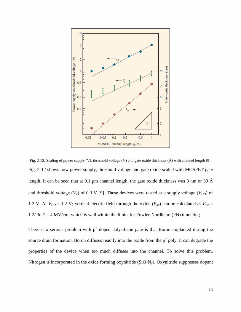
Fig. 2-12: Scaling of power supply (V), threshold voltage (V) and gate oxide thickness (Å) with channel length [9].
Fig. 2-12 shows how power supply, threshold voltage and gate oxide scaled with MOSFET gate
length. It can be seen that at 0.1 µm channel length, the gate oxide thickness was 3 nm or 30 Å
and threshold voltage (VT) of 0.3 V [9]. These devices were tested at a supply voltage (VDD) of
1.2 V. At VDD = 1.2 V; vertical electric field through the oxide (Eox) can be calculated as Eox =
1.2/ 3e-7 = 4 MV/cm; which is well within the limits for Fowler-Nordheim (FN) tunneling.
There is a serious problem with p+ doped polysilicon gate is that Boron implanted during the
source drain formation, Boron diffuses readily into the oxide from the p+ poly. It can degrade the
properties of the device when too much diffuses into the channel. To solve this problem,
Nitrogen is incorporated in the oxide forming oxynitride (SiOxNy). Oxynitride suppresses dopant

17
diffusion from polysilicon gate to the channel and from channel to gate oxide and prevents
threshold voltage shift due to Boron penetration.
Nitrogen incorporation in the oxide also reduces the effect of hot-electron based degradation of
the dielectric. Side benefits are and increased dielectric constant and hence improved gate
capacitance.
2.4.3 POLY GATE FORMATION
To attain 100 nm effective channel length (Leff), literature values show that the actual poly length
should be ~0.15 µm. The minimum feature size of a projection system is defined as CD =
k1λ/NA; where k1 is a constant depending on the type of lens in the projection system, λ is the
wavelength of illumination source and NA is the numerical aperture. For a given wavelength,
lithography comes to physical barrier to reduce feature size further. RIT SMFL is equipped with
an ASML make PAS5500 i-line (365 nm) stepper which has a minimum resolution of 0.35 µm.
This means that 0.35 µm size is the smallest features that the stepper can print in a single
exposure step.
To attain smaller feature sizes, Resolution Enhancement Techniques (RETs) are incorporated.
RETs include Optical Proximity Correction (OPC), Phase Shift Masks (PSM), Off Axis
Illumination (OAI), Source Mask Optimization (SMO), Double Exposure Lithography (DEL)
and Double Patterning Lithography (DPL).

18
Fig. 2-13: RETs at (a) 250 nm (b) 180 nm and (c) 90 nm and below [12].
When resolving very small feature size, loss of sharp features is observed like corner rounding
which leads to differences in the designed features and printed features. Serifs are added to the
corners of such features during mask design for overdose compensation. This is called “OPC”.
The semiconductor industry incorporated the use of OPC masks at 180 nm technology node.
This is represented in the center of Fig. 2-13 above.
“PSM” is a technique incorporated in photomasks that take advantage of interference generated
by phase difference to improve image resolution in photolithography. The industry used OPC +
PSM at 90 nm and below technology nodes [12]. This is represented on the right of Fig. 2-13
above.
Incorporation of these techniques involves computational lithography which is a major research
area by itself. It adds complexity to the mask design process and is not feasible for the current
work.
DEL and DPL lithography are techniques to obtain smaller feature sizes than those printed on the
photo mask. Both techniques have pros and cons depending on their application.

19
Fig. 2-14: Double Exposure Lithography (DEL) Process [10].
The process flow of DEL is depicted in the Fig. 2-14 above. DEL involves two exposure passes
without the wafer being removed from the exposure tool chuck between the subsequent passes.
Fig. 2-15: Double Patterning Lithography (DPL) Process [10].
The process flow during DPL is shown in the Fig. 2-15 above. As seen, this process involves
chemical development of photoresist between two exposure passes as well as an additional etch
step. This is commonly known as Litho-Etch-Litho-Etch (LELE) technique and is widely used in
the industry [10].
For the current CMOS process, DEL is advantageous as it gives better overlay control as the
wafers are not removed from the exposure chuck between subsequent exposure passes. Hence
processing time is low and high throughput is obtained. Less lithography steps also implies lower
cost of production.

20
Fig. 2-16: Pictorial representation of Double Exposure Lithography (left) top-down view, (right) cross section view, (top) after first exposure, (bottom) after second exposure.
The procedure shown in Fig. 2-14 is slightly different from that shown in Fig. 2-16. Fig. 2-14 is
about forming lines and spaces, while Fig. 2-16 is about reducing the length of a polysilcon line
by exposing once, shifting stage and expose again. Left side of Fig. 2-16 shows top-down view
and the right side shows cross-section view of the polysilicon gate during the double exposure
process. The mask defined poly length is 1 µm. There are three different variations in the width
of the polysilicon gate – 4/ 8/ 16 µm. After the first exposure, the pattern with 1 µm feature as
shown on top part of Fig. 2-16 will be transferred to the photoresist. The bleached photoresist
and the unexposed photoresist pattern can be seen in the cross-section view. The desired
polysilicon length is 0.15 µm. After the first exposure the stage is shifted in the Y-direction by
the desired amount (0.80 µm, refer to section 5.1.1 to learn more) and the wafer is exposed again.

21
The bottom portion of Fig. 2-16 shows the views of pattern on the photoresist after both the
exposures.
Once the pattern is transferred to the photoresist using double exposure lithography, the
developed resist acts as a hard-mask for the polysilicon etch process. When etching such small
features, it is crucial to maintain aspect ratio while etching. Aspect Ratio (AR) is defined as the
quotient of the depth (thickness) to width of the feature. In this case AR = 5/3.
Fig. 2-17: (a) Perfectly Anisotropic Etch (b) Isotropic poly etch.
Anisotropy in the etch profile is highly desired as shown in Fig. 2-17 (a) above. So the poly
features are etched using Reactive Ion Etch (RIE) technique. Isotropic etch profile is shown in
Fig. 2-17 (b). If the polysilicon etch is isotropic, the trapezoid shaped polysilicon wouldn’t be
completely thick enough to mask the channel from the source-drain implants. In this case Leff is
compromised. Etch should be uniform across the wafer surface. It should also have high
selectivity with the underlying thin gate oxide; else it would rapidly etch into the silicon where
the source drain regions are to be formed.

22
Chapter 3
Process Development
Three wafers are obtained to form a lot. The lot is numbered F140214. The standard factory lot
numbering format is FYYMMDD, where YY is the last two digits of the year, MM is month and
DD is the date on which the lot was started. Initial F stands for “Factory”. Research lots start
with the initial “R”, and scrapped lots begin with “S”. The lot number is exposed and patterned
on the top flat of the wafer during the first photo step.
3.1 Step-1: Pad Oxide Growth
500 Å pad oxide is thermally grown in the Bruce Furnace TUBE 04. Recipe #250 is used to
obtain the desired silicon oxide of 500 Å thickness. Thermal oxide growth in O2 ambient is much
slower than in H2O, so combination of higher temperatures and/or longer times are required to
obtain the desired oxide thickness.
Silicon Nitride is deposited in the next step. The nitride is highly stressed under tensile stress.
This results in a large compressive stress on the underlying silicon substrate if the pad oxide was
not present thus preventing defect generation. So it is called the “pad” oxide which acts as a
stress relief layer between the silicon nitride and silicon. Thermally grown SiO2 layers are under
compressive stress and Si3N4 layers are under tensile stress. Both of them partially compensate
for each other reducing stress on the substrate.

23
Fig. 3-1: Pad Oxide Growth.
Details of recipe #250 are shown in table 3-1. Oxide on silicon measurement program (81-point)
is used on the SpectraMap spectrophotometer to measure the oxide thickness and uniformity of
the measured data can be recorded in the form of 3D plot.
Table 3-1: Furnace recipe details.
Recipe Step Time (min) Temp (°C) Push In 12 800 Stabilize 15 800 Ramp up 30 1000 Soak 56 1000 N2 Purge 05 1000 Ramp Down 60 800 Pull Out 15 800
3.2 Step 2: LPCVD Silicon Nitride
Silicon nitride (1500 Å) is then deposited by Low Pressure Chemical Vapor Deposition
(LPCVD) in the lower tube of the ASM LPCVD furnace. Recipe Factory Nitride 810 is used.
Fig. 3-2 shows the cross section of the CMOS after the silicon nitride deposition step.
P type substrate (Resistivity 20 Ω-cm)
500 Å Pad oxide

24
Fig. 3-2: CVD Nitride Deposition.
The details of factory Nitride 810 recipe are recorded in the table below. The deposition occurs
in presence of reactants like ammonia NH3 and Silane SiH4 introduced in a furnace at 810 °C
temperature, forming silicon nitride Si3N4 through the following chemical reaction.
3𝑆𝑖3𝑁4 + 4𝑁𝐻3 → 𝑆𝑖3𝑁4 + 12𝐻2
The resulting silicon nitride thickness as well as uniformity is measured on the Prometrix SM300
spectrophotometer using the Nitride on oxide recipe. The underlying oxide thickness needs to be
entered.
The log sheet on the ASM LPCVD tool needs to be referred to obtain the latest deposition rates,
and the deposition time can be altered based on the desired thickness.
Table 3-2: LPCVD Nitride recipe parameters.
Pressure 300 mT Temperature 810 °C NH3 flow 150 sccm SiH2Cl2 flow 60 sccm Deposition Time 25 minutes
1500 Å Nitride
P type substrate
500 Å Pad oxide

25
3.3 Step 3: Photo 1: Active (Recessed Oxide)
The next step is isolating active areas from field areas. A layer of photoresist is used for
masking. Photoresist OiR 620-10 is spin coated on the wafer at room temperature. HMDS
priming is performed prior to spin-coat to ensure adhesion with the underlying layer. The final
resist thickness is a function of the viscosity of the resist and the spin speed. Recipe
“COAT.RCP” is used on the SSI track and wafers are baked at 110 °C to drive off the solvents
from the layer.
The wafers are next exposed on the ASML PAS 5500 i-line (365 nm) 5x reduction stepper using
the ADV STI maskset and fac_adv_cmos as the stepper job-name. A “stepper” exposes a small
area on the wafer during each exposure and then steps to the adjacent field to expose.
Fig. 3-3: Active (Recessed Oxide).
Photoresist materials are composed of complex hydrocarbon compounds. Only a certain part of
the photoresist material forms the photosensitive part, which is sensitive to ultra violet (UV)
500 Å Pad oxide1500 Å Nitride 1 µm Photoresist
P type substrate

26
light. This photosensitive material when exposed to UV light absorbs photons and changes its
chemical structure. This exposed part of the photoresist is then dissolved in developing solution.
“DEVELOP.RCP” recipe is used on the SSI track and the resulting structure looks like that
shown in Fig 3-3. Note that the axis are not to scale in the cross-sections depicted in this section.
The coat and develop recipes on the SSI track are as described in the Fig 3-4 below.
Fig. 3-4: Coat and Develop recipe parameters for the SSI track.
The thickness of photoresist obtained using the coat recipe is 1 µm. This photoresist is thick
enough to mask the nitride underneath during plasma etch.
3.4 Step 4: Etch Nitride
After the pattern is defined in the photoresist, silicon nitride is etched by dry etching in fluorine
plasma chemistry, and the resist acts a masking layer. This is accomplished in the LAM 490
using SF6 gas. The following reaction takes place.
HMDS Vapor Prime140 °C, 60 sec.
OiR 620-10 resist3250 RPM, 30 sec 90 °C, 60 sec
140 °C, 60 sec
DI WetCD-26 Developer
50 sec Puddle30 sec Rinse
30 sec, 3750 RPM SRD
110 °C, 60 sec
Dehydrate bake/ HMDS Priming
Develop Hard BakePost Exposure Bake
Spin Coat Soft bake
Resist thickness: 1 µm

27
𝑆𝑖3𝑁4 + 12𝐹 → 3𝑆𝑖𝐹4 + 12𝑁2
Fig. 3-5: Nitride plasma etching recipe parameters.
Optical endpoint detection technique is used on the LAM 490 to check for the selectivity with
the underlying pad oxide. The cross section after etching is as shown in Fig. 3-5 above. Over
etch into pad oxide is carried out to ensure nitride is not present field areas. The recipe
parameters are as shown in Table 3-3 below.
Table 3-3: Nitride plasma etch recipe parameters.
Recipe Name FNIT1500.RCP Gap 1.65 SF6 flow 200 sccm Pressure 260 mTorr Step 1 RF=0; T=1min Step 2 RF=125; T=2:30min Step 3 RF=125; Overetch=40%
500 Å Pad oxide1500 Å Nitride 1 µm Photoresist
250 Å Pad oxide
P type substrate

28
3.5 Step 5: Photoresist Strip
After plasma etching of the nitride, the photoresist is etched in oxygen plasma on the Gasonics
Aura 1000 asher. This doesn’t affect the underlying nitride. The recipe FF is used which runs for
180 seconds. The cross section after this step is as shown in Fig. 3-6 below.
Fig. 3-6: Photoresist Strip.
Details of the recipe are shown in the table below. The wafers can be inspected visually or under
the microscope to ensure that the photoresist is completely ashed.
3.6 Step 6: RCA Clean
The wafers are then cleaned to get rid of residual photoresist particles. This step ensures that the
wafers are clean from particulate contamination before they go into the furnace for the
subsequent oxidation step.
The process used for cleaning the wafers is called RCA clean. RCA stands for Radio Corporation
of America that developed the process. This process helps remove organic and metallic particles
from the surface of the wafer.
500 Å Pad oxide1500 Å Nitride
250 Å Pad oxide
P type substrate
Active Area
Field Area

29
Two separate baths are utilized to carry out the clean. SC-1 bath contains a mixture of
Ammonium hydroxide (NH4OH) and Hydrogen Peroxide (H2O2) which help remove organic
particles from the wafer surface. The presence of H2O2 leads to native oxide growth on bare
silicon, which is etched in a 50:1 H2O:HF bath for 30 seconds. The SC-2 bath contains
hydrochloric acid (HCl) and hydrogen peroxide (H2O2) which helps remove metallic impurities.
This is followed by a spin-rinse-dry (SRD) to dry the wafers.
The process flow of RCA clean procedure is shown in the Fig. 3-7 below.
Fig. 3-7: General RCA clean procedure.
H2O – 5000 mlNH4OH – 300 mlH2O2 – 300 ml75 °C, 10 min
DI water rinse5 min
50:1 HF:H2O30 sec
DI water rinse5 min
H2O – 5000 mlHCl – 300 ml
H2O2 – 300 ml75 °C, 10 min
DI water rinse5 min
SPIN-RINSE-DRY (SRD)
APM
HPM

30
3.7 Step 7: Wet Oxide: First Recessed Oxide growth
Recessed oxide isolation technique will be used to isolate active areas. 3500 Å wet oxide is
grown in the field area as shown in the figure. During this process, 1610 Å of silicon is
consumed. The resulting oxide is represented in the cross-section shown in Fig. 3-8 below.
Fig. 3-8: Wet oxide: First recessed oxide growth.
Recipe #336 on the Bruce furnace TUBE 01 is used which yields 3500 Å oxide. The details of
recipe are as shown in Table 3-4 below.
Table 3-4: Bruce furnace recipe parameters for first recessed oxide growth.
Recipe Step Time (min) Temp (°C) Push In 12 800 Stabilize 15 800 Ramp up 30 1100 Soak 360 1100 N2 Purge 05 1100 Ramp Down 60 800 Pull Out 15 800
500 Å Pad oxide1500 Å Nitride
3500 Å LOCOS Oxide
P type substrate
Active Area
Field Area
(0.46)Xox= 1610 Å
(0.54)Xox= 1890 Å

31
3.8 Step 8: Oxide Etch
The oxide grown in the previous step is then etched off in 10:1 Buffered HF BOE solution. Etch
rate is found to be 586 Å/min. A BOE dip for 6 minutes 30 seconds ensures that all the oxide is
etched off. This is followed by rinse in DI water and spin-rinse-dry (SRD). Step height in silicon
is found to be 1610 Å as illustrated in the cross section shown in Fig. 3-9 below.
Fig. 3-9: Oxide etch.
3.9 Step 9: Wet Oxide: Second Recessed Oxide
A second wet oxide (3500 Å) is grown in the trench formed in the previous step. This is carried
out in the Bruce furnace TUBE 01 using the same recipe #336. Silicon (1610 Å) is further
consumed during this step and 3500 Å of field oxide is obtained which is co-planar with the
active areas. The cross section of the resulting structure is as shown in Fig, 3-10 below.
500 Å Pad oxide1500 Å Nitride
P type substrate
(0.46)Xox= 1610 Å

32
Fig. 3-10: Wet oxide: second recessed oxide.
3.10 Step 10: Nitride Etch in Hot Phosphoric acid
Nitride that is left over in the active areas is etched in hot phosphoric acid at 165 °C. Etch rate of
nitride is 80 Å/ min and nitride is etched for 45 min to ensure complete etch. Bath should be
constantly stirred and agitation should be provided to the bath to ensure uniform temperature
throughout the bath, else the etch rate is non-uniform.
Fig. 3-11: Nitride etch in hot phosphoric acid.
500 Å Pad oxide1500 Å Nitride
3500 Å Recessed Oxide
P type substrate
(0.46)Xox= 1610 Å
(0.54)Xox= 1890 Å
500 Å Pad oxide
3500 Å Recessed Oxide
P type substrate

33
Good selectivity is observed over the underlying pad oxide. The CMOS cross-section after
nitride etching is as shown in Fig 3-11.
3.11 Step 11: Photo 2 - N-Well
Next step is photo for N-well implant. A layer of photoresist is used for masking the P-well from
this implant. Photoresist OiR 620-10 is spin coated on the wafer using recipe “COATMTL.RCP”
on the SSI track and wafers are baked at 90 °C.
The wafers are next exposed on the ASML PAS 5500 i-line (365 nm) 5x reduction stepper using
the ADV NWELL maskset, fac_adv_cmos as the stepper job-name and NWELL as the layer ID.
The exposed resist is then developed using “DEVMTL.RCP” recipe on the SSI track and the
resulting structure looks like that shown in Fig 3-12.
Fig. 3-12: N-well photo.
500 Å Pad oxide
3500 Å Recessed Oxide
P type substrate
1.3 µm Photoresist

34
The resulting photoresist using COATMTL recipe is 1.3 µm thick and enough to mask the P-
well beneath the photoresist from the N-well implants.
The COATMTL and DEVMTL recipes on the SSI track are shown in Fig. 3-13 below.
Fig. 3-13: Coatmtl and devmtl recipes on the SSI track.
Wafers are then inspected on the microscope to check for CD, resolution and X and Y alignment
errors.
3.12 Step 12: N-well Implant
The N-well implant is carried out through the 500 Å pad oxide that masks the active areas.
Phosphorous (P31) is implanted using the Varian 350D ion-implanter at 170 keV and dose of
5e13 cm-2. Fig 3-14. shows the cross section of the CMOS during the N-well implant. The
regions where the P-well is to be formed is covered by 1.3 µm thick resist which is enough to
mask the underlying layer from the Phosphorous implant.
H2O – 5000 mlNH4OH – 300 ml
H2O2 – 300 ml75 °C, 10 min
OiR 620-10 resist3250 RPM, 30 sec 90 °C, 60 sec
DI water rinse5 min
H2O – 5000 mlHCl – 300 mlH2O2 – 300 ml75 °C, 10 min
110 °C, 60 sec
Dehydrate bake/ HMDS Priming
Develop Hard BakePost Exposure Bake
Spin Coat Soft bake
Resist thickness: 1 µm

35
Fig. 3-14: N-well implant.
If the doping is too light under the field oxide, surface inversion can occur in these regions and
can short back to back MOS devices. By ensuring that well implants penetrate beneath the field
oxide, the parasitic inversion problem is prevented.
3.13 Step 13: Photoresist Strip
The photoresist is ashed in the Gasonics asher using “FF” recipe. The wafers are inspected
visually or on the microscope to make sure resist has completely ashed. The cross-section after
this step is as shown in Fig. 3-15 below.
500 Å Pad oxide
3500 Å Recessed Oxide
P31, 5e13 cm-2 @170 keV
P type substrate
1.3 µm Photoresist

36
Fig. 3-15: Photoresist Strip.
3.14 Step 14: Photo 3 – P-well
Next step is photo for P-well implant. A layer of photoresist is used for masking the N-well from
this implant. Photoresist OiR 620-10 is spin coated on the wafer using recipe “COATMTL.RCP”
on the SSI track and wafers are baked at 90 °C.
The wafers are next exposed on the ASML PAS 5500 i-line (365 nm) 5x reduction stepper using
the ADV NWELL maskset, fac_adv_cmos as the stepper job-name and PWELL as the layer ID.
The exposed resist is then developed using “DEVMTL.RCP” recipe on the SSI track and the
resulting structure looks like that shown in Fig 3-16.
500 Å Pad oxide
P type substrate
3500 ÅRecessed Oxide
1e14 cm-2, 170 keV, P31
P type substrate
500 Å Pad oxide
3500 Å Recessed Oxide

37
Fig. 3-16: P-well photo.
The resulting photoresist using COATMTL recipe is 1.3 µm thick and enough to mask the N-
well beneath the photoresist from the P-well implants.
Wafers are then inspected on the microscope to check for CD, resolution and X and Y alignment
errors.
3.15 Step 15: P-well Implant
The P-well implant is carried out through the 500 Å pad oxide that masks the active areas. Boron
(B11) is implanted using the Varian 350D ion-implanter at 170 keV and dose of 7e13 cm-2. Fig
3-17. shows the cross section of the CMOS during the P-well implant. The regions where the N-
well is to be formed is covered by 1.3 µm thick resist which is enough to mask the underlying
layer from the Boron implant.
500 Å Pad oxide
3500 Å Recessed Oxide
P31, 5e13 cm-2 @170 keV
P type substrate
1.3 µm Photoresist

38
Fig. 3-17: P-well implant.
As discussed during the N-well implant, the P-well implant should also penetrate beneath the
field oxide to increase the doping in the region and prevent parasitic inversion problem.
3.16 Step 16: Photoresist Strip
The photoresist is ashed in the Gasonics asher using “FF” recipe. The wafers are inspected
visually or on the microscope to make sure resist has completely ashed.
B11, 7e13 cm-2 @100 keV
P type substrate
1.3 µm Photoresist
3500 Å Recessed Oxide
P31, 5e13 cm-2 @170 keV
39
Fig. 3-18: Photoresist strip.
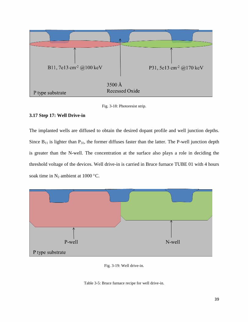
3.17 Step 17: Well Drive-in
The implanted wells are diffused to obtain the desired dopant profile and well junction depths.
Since B11 is lighter than P31, the former diffuses faster than the latter. The P-well junction depth
is greater than the N-well. The concentration at the surface also plays a role in deciding the
threshold voltage of the devices. Well drive-in is carried in Bruce furnace TUBE 01 with 4 hours
soak time in N2 ambient at 1000 °C.
Fig. 3-19: Well drive-in.
Table 3-5: Bruce furnace recipe for well drive-in.
40
Recipe Step Time (min) Temp (°C) Push In 12 800 Stabilize 15 800 Ramp up 30 1100 Soak 240 1100 N2 Purge 05 1100 Ramp Down 60 800 Pull Out 15 800
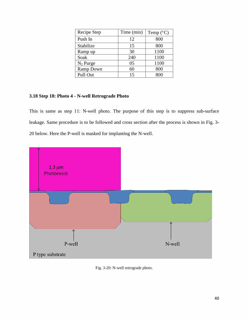
3.18 Step 18: Photo 4 - N-well Retrograde Photo
This is same as step 11: N-well photo. The purpose of this step is to suppress sub-surface
leakage. Same procedure is to be followed and cross section after the process is shown in Fig. 3-
20 below. Here the P-well is masked for implanting the N-well.
Fig. 3-20: N-well retrograde photo.

41
3.19 Step 19: N-well Retrograde Implant
Phosphorous P31 is implanted to the N-well at 9e13 cm-2 dose at 70 keV. The peak of the implant
profile is placed such that it prevents sub-surface punchthrough.
Fig. 3-21: N-well retrograde implant.
3.20 Step 20: Photoresist Strip
The photoresist is ashed in the Gasonics asher using “FF” recipe. The wafers are inspected
visually or on the microscope to make sure resist has completely ashed. The resulting cross-
section is shown in Fig. 3-22.

42
Fig. 3-22: Photoresist Strip.
3.21 Step 21: Photo 5 - P-well Retrograde Photo
Photo step is repeated as carried out for P-well in Step 14. The wafers are patterned with
photoresist so as to mask the N-well regions from the P-well retrograde implant in the
subsequent step. Cross section of CMOS after this step is shown in Fig. 3-23 below.
Fig. 3-23: P-well retrograde photo.

43
3.22 Step 22: P-well Retrograde Implant
B11 is implanted on the wafers on the Varian 350D implanter with a dose of 1e14 cm-2 at 45 keV.
This implant prevents sub-surface punchthrough.
Fig. 3-24: P-well retrograde implant.
3.23 Step 23: Photoresist Strip
The photoresist is ashed in the Gasonics asher using “FF” recipe. The wafers are inspected
visually or on the microscope to make sure resist has completely ashed.
Fig. 3-25: Photoresist Strip.

44
3.24 Step 24: Pad Oxide Etch
The 500 Å pad oxide above the active areas needs to be removed before the gate oxide growth. 1
minute etch in 10:1 BOE which has a etch rate of 560 Å/min does the job. This is followed by a
DI rinse in H2O for 5 minutes and SRD.
Fig. 3-26: Pad Oxide Etch.
3.25 Step 25: RCA Clean
RCA Clean is performed prior to putting the wafers in the furnace for gate oxide growth. The
same procedure as used before is used for the RCA clean. It is important to get rid of organic and
metallic impurities from the wafer surface prior to the gate-oxide growth, to ensure desired
threshold voltage.
3.26 Step 26: Native Oxide Etch
A 1 minute dip in 50:1 HF ensures there is no native oxide on the active areas. When dealing
with very thin gate oxides, this step is crucial.

45
3.27 Step 27: Dry Oxide- Gate Oxide Growth
The thin gate oxide acts as s dielectric insulating the polysilicon gates from the channel region.
The gate capacitance depends on the gate dielectric thickness and hence it plays a role in how
better control the gate has over the channel region. 30 Å gate oxide is to be grown with N2O
incorporation to prevent Boron penetration through the gate oxide and increasing the effective
dielectric constant.
The gate oxide is grown in Bruce Furnace TUBE 04. The tube is first warmed up to 800 °C and
then Recipe #463 SMFL TransLC Clean recipe is run (~1 hour) to get rid of Sodium
contamination in the tube which can form interface trapped charges in the gate oxide. After this
run is completed, the wafers are loaded in the tube and Recipe #213 for 30 Å gate oxide is run.
The details of this recipe are: R/U 20 min from 800 to 900 °C, 10 min in dry O2 at 900 °C, 10
min soak in N2O at 900 °C, R/D 40 min.
Fig. 3-27: Dry oxide – gate oxide growth.

46
Table 3-6: Bruce furnace recipe for gate oxide growth.
Recipe Step Time (min) Temp (°C) Push In 12 650 Stabilize 30 650 Ramp up 30 900 Soak N2O 10 900 Soak O2 10 900 Ramp Down 30 650 Pull Out 15 25
The resulting gate oxide is too thin to be measured on a spectrophotometer or Variable Angle
Spectroscopic Ellipsometer (VASE). This was a critical step during processing and the reason is
explained later in section 5.2.
3.28 Step 28: LPCVD Polysilicon
Polysilicon is then deposited by low pressure chemical vapor deposition (LPCVD) process in the
lower tube of the ASM LPCVD tool. Recipe FACPOLY610 is used to deposit poly. The
thickness of polysilicon should be enough to mask the channel region from source/drain
implants. The deposition time for 2500 Å Polysilicon is 37 minutes.
Fig. 3-28: LPCVD Polysilicon deposition.

47
A dummy wafer with oxide needs to be incorporated during the run and polysilicon thickness
can be measured on the Prometrix SM300 SpectraMap.
3.29 Step 29: Photo 6 – Poly Gate – Double Exposure.
The double exposure process to be used has already been explained in detail in chapter 2 section
2.4.3 and shall not be repeated here again. The devices on the wafer to be double exposed must
be aligned with the direction of shift, which is Y-axis in this case. Both the exposures are carried
with 190 mJ/cm2 exposure dose.
Fig. 3-29: Poly photo.
3.30 Step 30: Poly Gate RIE
The patterned polysilicon is now etched on the Drytek Quad reactive ion etcher. When etching
such small features, high anisotropy in the etch profile is desired so the exact pattern on the

48
photoresist is transferred to the polysilicon. The CMOS cross section after the desired polysilicon
etch is as shown in the Fig 3-20. Recipe FACPOLY is used for 2:45 minutes to etch poly.
Fig. 3-30: Poly gate RIE.
The resulting polysilicon gate with such small dimensional features can only be measured on
LEO SEM. Details of the etching recipe are shown in table 3-7 below.
Table 3-7: Poly etch recipe details.
Recipe Name FACPOLY Chamber 2 Power 160 Watts Pressure 40 mTorr SF6 gas flow 30 sccm CHF3 gas flow 30 sccm O2 gas flow 5 sccm
3.31 Step 31: Photoresist Strip

49
The photoresist is ashed in the Gasonics asher using “FF” recipe. The wafers are inspected
visually or on the microscope to make sure resist has completely ashed.
Fig. 3-31: Photoresist Strip.
3.32 Step 32: RCA Clean
RCA clean is performed prior to the polysilicon re-oxidation to get rid of organic impurities from
the photoresist.
3.33 Step 33: Poly Re-oxidation
Once the polysilicon gates are etched, there is damage induced to the sides of the polysilicon
which needs to be repaired. The poly re-oxidation step serves the purpose of repairing the edges
of the gate which could lead to unwanted capacitance between gate and channel. Poly re-ox also
acts as a screen oxide during the source drain implants reducing channeling into the silicon as
well as polysilicon gates. Nitride sidewall spacers will be formed after the LDD implants. The

50
poly re-oxidation also acts as a pad-oxide or stress relief layer between the nitride-poly and
nitride-silicon interfaces. 250 Å thermal oxide is grown during the poly re-oxidation.
Fig. 3-33: Polysilicon re-oxidation.
Table 3-8: Bruce Furnace recipe details.
Recipe Step Time (min) Temp (°C) Push In 12 800 Stabilize 15 800 Ramp up 10 900 Soak 93 900 N2 Purge 05 900 Ramp Down 20 800 Pull Out 15 25
3.34 Step 34: Photo 6 - NLDD Photo
Next step is photo for NLDD implant. A layer of photoresist is used for masking the PMOS from
this implant. Photoresist OiR 620-10 is spin coated on the wafer using recipe “COAT.RCP” on
the SSI track and wafers are baked at 90 °C.

51
The wafers are next exposed on the ASML PAS 5500 i-line (365 nm) 5x reduction stepper using
the ADV NLDD maskset, fac_adv_cmos as the stepper job-name and NLDD as the layer ID.
The exposed resist is then developed using “DEVELOP.RCP” recipe on the SSI track and the
resulting structure looks like that shown in Fig 3-34.
The resulting photoresist using COAT recipe is 1 µm thick and enough to mask the PMOS
beneath the photoresist from the NLDD implants.
Wafers are then inspected on the microscope to check for CD, resolution and X and Y alignment
errors.
Fig 3-34.: NLDD Photo.
3.35 Step 35: NLDD implant

52
The N-LDD implant is carried out through a 250 Å poly re-ox. These are the low energy
implants and yield very shallow junctions. Arsenic atom is heavier than Phosphorous and hence
lower scattering is observed in Arsenic implants. Lower effect of Transient Enhanced Diffusion
(TED) is also observed when Arsenic implants are carried out compared to Phosphorous. But
Arsenic being poisonous, we don’t have Arsenic capability in the Varian 350D implanter at RIT.
Hence we implant Phosphorous (P31) instead. Wafers need to be packed and sent out for Arsenic
implants in the future to make smaller devices work. The Arsenic implant need to be carried out
with a dose of 5e15 cm-2 at 20 keV.
Fig. 3-35: NLDD implant.
3.36 Step 36: Photoresist Strip

53
The photoresist is ashed in the Gasonics asher using “FF” recipe. The wafers are inspected
visually or on the microscope to make sure resist has completely ashed. The cross section after
this step is shown in Fig. 3-36.
Fig. 3-36: Photoresist strip.
3.37 Step 37: Photo 8 – PLDD Photo
Next step is photo for PLDD implant. A layer of photoresist is used for masking the NMOS from
this implant. Photoresist OiR 620-10 is spin coated on the wafer using recipe “COAT.RCP” on
the SSI track and wafers are baked at 90 °C.
The wafers are next exposed on the ASML PAS 5500 i-line (365 nm) 5x reduction stepper using
the JG PLDD maskset, fac_adv_cmos as the stepper job-name and PLDD as the layer ID.
The exposed resist is then developed using “DEVELOP.RCP” recipe on the SSI track and the
resulting structure looks like that shown in Fig 3-37. The resulting photoresist using COAT
recipe is 1 µm thick and enough to mask the NMOS beneath the photoresist from the PLDD
implants. Wafers are then inspected on the microscope to check for CD, resolution and X and Y
alignment errors.

54
Fig. 3-37: PLDD photo.
3.38 Step 38: PLDD Implant
Fig. 3-38: PLDD implant.

55
Similar to the N-LDD implants, the P-LDD implants are carried out through the 250 Å poly re-
ox BF2 species of Boron. Wafers are implanted with a dose of 9e14 cm-2 with 20 keV energy.
3.39 Step 39: Photoresist Strip
The photoresist is ashed in the Gasonics asher using “FF” recipe. The wafers are inspected
visually or on the microscope to make sure resist has completely ashed.
Fig. 3-39: Photoresist Strip.
3.40 Step 40: RCA Clean
RCA clean is performed prior to Nitride deposition to make sure there are no leftover organic
impurities from the photoresist. This helps maintain uniformity in the nitride film to be
deposited.
3.41 Step 41: LPCVD Nitride
2500 Å nitride is then deposited to form sidewall spacers. This is carried out in the lower tube of
the ASM LPCVD tool. Factory Nitride 810 recipe is used to obtain the desired thickness of 2500

56
Å. The log sheet besides the tool must be observed to obtain the deposition rates from recent
runs. Cross-section of the CMOS after this step is shown in Fig. 3-40 below.
Fig. 3-40: LPCVD Nitride deposition.
Table 3-9: Recipe details for nitride sidewall spacer deposition.
Pressure 300 mT Temperature 810 °C NH3 flow 150 sccm SiH2Cl2 flow 60 sccm Deposition Time 55 minutes
3.42 Step 42: Etch Nitride
Nitride is then etched using RIE in the Drytek Quad to obtain sidewall spacers around the
polysilicon. The 250 Å oxide grown during the poly re-ox beneath the nitride in active areas acts
as an etch stop layer to prevent etching of the silicon beneath where shallow source drain are to
be formed. The length of the sidewall spacer is defined by the thickness of the CVD Nitride. As
the RIE is anisotropic, the height of the spacer should be same as the length of the spacer. The
length of the side wall spacer should be enough to check for lateral diffusion of the source drain

57
implants. This would reduce the overall length of the LDD and increase hot electron effects at
the drain end. Cross-section of the CMOS after this step is shown in Fig. 3-41 below.
FACADVSP recipe is used on the Drytek Quad with etch time 02:30 minutes.
Fig. 3-41: RIE Nitride.
Table 3-10: RIE nitride.
Recipe Name FACSPCR Chamber 2 Power 250 Watts Pressure 40 mTorr SF6 gas flow 30 sccm
3.43 Step 43: Photo 9 – Photo N+ DS
Next step is photo for N+ DS implant. A layer of photoresist is used for masking the PMOS from
this implant. Photoresist OiR 620-10 is spin coated on the wafer using recipe “COAT.RCP” on
the SSI track and wafers are baked at 90 °C.

58
The wafers are next exposed on the ASML PAS 5500 i-line (365 nm) 5x reduction stepper using
the ADV N+ DS maskset, fac_adv_cmos as the stepper job-name and N+ DS as the layer ID.
The exposed resist is then developed using “DEVELOP.RCP” recipe on the SSI track and the
resulting structure looks like that shown in Fig 3-42.
The resulting photoresist using COAT recipe is 1 µm thick and enough to mask the PMOS
beneath the photoresist from the N+ DS implants.
Wafers are then inspected on the microscope to check for CD, resolution and X and Y alignment
errors.
Fig. 3-42: N+ DS Photo.

59
3.44 Step 44: Implant N+ DS
The N+ DS implants are carried out through the oxide remaining over the channel region after the
nitride sidewall spacer etch. Similar to the LDD implants the S-D implants are self-aligned to the
poly gate. The NMOS has N+ poly gate that control the charge in the channel. Ultra shallow
junction formation requires Arsenic dopants instead of Phosphorous as discussed earlier. The
implants should be shallow so that the lateral diffusion during the anneal step doesn’t consume
the LDD implants or consume the channel region. Arsenic needs to be implanted with a dose of
1e15 cm-2 with 25 keV energy. As Arsenic is not available at RIT, P31 was implanted.
Fig. 3-43: Implant N+ DS.
3.45 Step 45: Photoresist Strip
The photoresist is ashed in the Gasonics asher using “FF” recipe. The wafers are inspected
visually or on the microscope to make sure resist has completely ashed.

60
Fig. 3-44: Photoresist Strip.
3.46 Step 46: Photo 10 – P+ DS
Next step is photo for P+ DS implant. A layer of photoresist is used for masking the NMOS from
this implant. Photoresist OiR 620-10 is spin coated on the wafer using recipe “COAT.RCP” on
the SSI track and wafers are baked at 90 °C.
The wafers are next exposed on the ASML PAS 5500 i-line (365 nm) 5x reduction stepper using
the JG P+ DS maskset, fac_adv_cmos as the stepper job-name and P+ DS as the layer ID.
The exposed resist is then developed using “DEVELOP.RCP” recipe on the SSI track and the
resulting structure looks like that shown in Fig 3-45.
The resulting photoresist using COAT recipe is 1 µm thick and enough to mask the NMOS
beneath the photoresist from the P+ DS implants.
Wafers are then inspected on the microscope to check for CD, resolution and X and Y alignment
errors.

61
Fig. 3-45: P+ DS photo.
3.47 Step 47: Implant P+ DS
The P+ DS regions are implanted through the 250 Å oxide left over after the nitride sidewall
spacer etch. The implants are self-aligned to the poly gate and form P+ poly gate for the PMOS
transistors. Ultra shallow junctions need to be formed so that the LDD regions are not consumed
by the source-drain after anneal. BF2 ions being heavier compared to the B11 would check for
scattering during the implant so that shallow junctions are obtained. Implants are carried out on
the Varian 350 D implanted with a dose of 5e15 cm-2 at energy of 27 keV and keeping into
consideration the effects of TED. Cross-section of the CMOS after this step is shown in Fig. 3-46
below.

62
Fig. 3-46: Implant P+ DS.
3.48 Step 48: Photoresist Strip
The photoresist is ashed in the Gasonics asher using “FF” recipe. The wafers are inspected
visually or on the microscope to make sure resist has completely ashed.
Fig. 3-47: Photoresist Strip.

63
3.49 Step 49: RCA Clean
RCA clean is performed prior to anneal to make sure there are no organic residues from the
photoresist or metallic impurities on the surface that can get driven-in to the bulk.
3.50 Step 50: SD Anneal (RTP)
The dopants implanted into the source drain regions need to be electrically activated. The
implanted ions assume interstitial locations in the Si crystal lattice structure. When annealed,
they replace Silicon atoms in the lattice and provide free electrons and holes for conduction. This
called dopant activation.
The most general anneal method is to soak the wafers in the furnace in nitrogen ambient for a
long period. The effects of TED are exaggerated and the resulting junctions are not shallow as
desired. The heavier doped source drain implants tend to consume the LDD implants and even
penetrate in the channel region which is undesirable. Spike annealing is a better alternative to
this method. The wafers are annealed using Rapid Thermal Processor (RTP).
For this purpose we use the AG610 RTP tool. A new recipe is created which can R/U to 1050 °C
in 3 seconds; Soak in Nitrogen ambient at 1050 °C for 5 seconds; R/D to 25 °C in 6 seconds.
Two dummy runs are to be carried out to heat up the walls of the RTP chamber before doing the
actual run.
Cross-section of the CMOS after this step is shown in Fig. 3-48 below.

64
Fig. 3-48: SD anneal (RTP).
3.51 Step 51: Oxide Etch
This step involves preparing the surface of the wafer for Titanium deposition for Self Aligned
Silicide) SALICIDE formation. Cross-section of the CMOS after this step is shown in Fig. 3-49
below.
Fig. 3-49: Oxide etch.

65
3.52 Step 52: Titanium Deposition
Titanium is uniformly sputter deposited on the surface of the wafer. This Titanium is used to
selectively react with silicon and polysilicon and form Titanium Silicide (TISi2) in the
subsequent steps. Silicide formed in this manner is called Self Aligned siLICIDE(SALICIDE)
which has very low sheet resistance. The target thickness is 300 Å.
The sputter deposition is carried out on the CVC601 tool in the RIT SMFL using a 4” target. The
system is allowed to get to a base pressure < 5e-6 Torr by pumping down the chamber. Pre-
sputter using 4” target for 5 minutes at 350 W.
Cross-section of the CMOS after this step is shown in Fig. 3-50 below.
Table 3-11: Titanium sputter details.
Power 350 W Pressure < 5e-6 Torr Argon Pressure 5 mTorr Argon flow 17 sccm Sputter time 240 sec
Fig. 3-50: Titanium deposition.

66
3.53 Step 53: RTP 1 (TiSi)
Low temperature Rapid Thermal Anneal step is carried out in N2 ambient. Titanium selectively
reacts in areas where it has silicon and polysilicon beneath to form metal silicide and remains
unreacted in areas where there is oxide beneath. Metastable C49 phase high resistivity Titanium
Silicide is formed due to this reaction [11]. The low temperature of this step prevents lateral
diffusion of reacted Titanium, which could short the contacts. This can be seen in Fig. 3-51
below and unreacted Titanium remains in rest of the areas. Also low temperature RTP prevents
the shallow source drain regions from diffusion further.
Table 3-12: RTP 1 TiSi recipe details.
Recipe FACTiSi1 Ramp up 25 -650 °C in 5 sec Steady State 650 °C for 10 sec Argon flow 650 – 25 °C in 5 sec
Fig. 3-51: RTP1 – TiSi.

67
3.54 Step 54: Unreacted Ti Etch
Unreacted Titanium is then selectively etched in a solution of 1:2 H2SO4:H2O2 in a hot plate at
150 °C for 2 minutes. Titanium Silicide won’t etch but the unreacted Titanium would etch in the
chemistry. Fig. 3-52 shows the cross-section view after the removal of unreacted Titanium.
Fig. 3-52: Unreacted Titanium etch.
3.55 Step 55: RTP 2 (TiSi2)
The second RTA is carried out at a relatively higher temperature, in N2 ambient. This converts
the C49 phase Titanium Silicide to a C54 phase Titanium di-silicide which is more stable and has
lower resistivity [11]. Cross section of the CMOS after this step is shown in Fig. 3-53 below.
Details of the recipe on the RTA tool are shown in the Table 3-13 below.
Table 3-13: RTP 2 TiSi2 recipe details.
Recipe FACTiSi1 Ramp up 25 -700 °C in 5 sec Steady State 750 °C for 10 sec Argon flow 750 – 25 °C in 10 sec

68
Fig. 3-53: RTP 2 (TiSi2).
3.56 Step 56: PECVD TEOS
Before the first layer metal can be deposited, Tetraethyl orthosilicate (TEOS) is deposited on the
wafer which would prevent the metal lines from shorting the polysilicon lines beneath. This is
called the Inter Level Dielectric (ILD) or the 0th level dielectric in this case. 4000 Å thick TEOS
would be sufficient enough to cover the thickness of the polysilicon gate and also provide good
step coverage over the highly irregular topology beneath. The cross section of CMOS after the
TEOS deposition is as shown in the Fig. 3-54 below.
Fig. 3-54: CVD TEOS.

69
Table 3-14 shows the details of the recipe on the AME P5000.
Table 3-14: Details of PECVD TEOS recipe on P5000.
Recipe A6-FAC 0.4M TEOS Thickness desired 4000 Å Deposition time 61 sec
3.57 Step 57: Photo 11 – Contact Cut
Next step is photo for etching contact cuts. A layer of photoresist is coated and contact cut holes
are opened up as desired on the TEOS beneath it. Photoresist OiR 620-10 is spin coated on the
wafer using recipe “COAT.RCP” on the SSI track and wafers are baked at 90 °C.
The wafers are next exposed on the ASML PAS 5500 i-line (365 nm) 5x reduction stepper using
the JG CC maskset, fac_adv_cmos as the stepper job-name and CC as the layer ID.
The exposed resist is then developed using “DEVCC.RCP” recipe on the SSI track and the
resulting structure looks like that shown in Fig 3-55. The DEVCC is modified version of
DEVELOP recipe which has a longer develop time in the CD-26 developer as it needs to clear
the photoresist in the small holes.
The resulting photoresist using COAT recipe is 1 µm thick.
Wafers are then inspected on the microscope to check for CD, resolution and X and Y alignment
errors.

70
Fig. 3-55: Contact cut photo.
3.58 Step 58: Etch CC
Contact cuts are etched on the Drytek Quad RIE tool. Cuts need to etched to the bottom as the
contacts must have low-resistivity. Etching is carried out in CHF3, CF4 and Ar gas. Carbon-
Hydrogen polymer build up takes place at on the sidewalls of the contact cuts. The heavy Argon
ion helps increase the anisotropy during the etch process. O2 gas is also introduced during
etching which helps remove polymer build-up in the sidewalls of the contacts. There is a trade-
off in incorporating O2 gas in the chamber as it also etches photoresist that is masking the TEOS.
High selectivity during the etch process is desired [13]. A cross section of the CMOS after the
contact cut etch is shown in Fig. 3-56. Details of the FACCUT recipe on the Drytek Quad are
shown in Table 3-15.

71
Fig. 3-56: Contact cut etch.
Table 3-15: Contact cut etch recipe details.
Recipe Name FACCUT Chamber 3 Power 200 Watts Pressure 100 mTorr CHF3 gas flow 50 sccm CF4 gas flow 10 sccm Ar 100 sccm O2 5 sccm
3.59 Step 59: Photoresist Strip
The photoresist is ashed in the Gasonics asher using “FF” recipe. The wafers are inspected
visually or on the microscope to make sure resist has completely ashed.

72
Fig. 3-57: Photoresist Strip.
3.60 Step 60: RCA Clean
RCA clean is performed prior to metal deposition to ensure there are no left over organic or
metallic impurities on the surface. This ensures a uniform deposition of the metal.
Fig. 3-58: RCA clean.

73
3.61 Step 61: Metal 1 – Aluminum deposition
4000 Å of Aluminum with 1% Silicon is deposited to prevent junction spiking at the source,
drain and gate contacts. Al-Si is blanket deposited on the entire wafer which will form the metal
1. CVC 601 sputter tool is used to deposit Al-Si. The CMOS cross-section after Aluminum
deposition is shown in Fig. 3-59 below.
Fig. 3-59: Metal 1 – Aluminum deposition.
The sputter deposition is carried out on the CVC601 tool in the RIT SMFL using a 8” target. The
system is allowed to get to a base pressure < 5e-6 Torr by pumping down the chamber. Pre-
sputter using 8” target for 5 minutes at 2000 W. Details of the Aluminum sputter are as shown in
Table 3-16.
Table 3-16: Aluminum sputter details.
Power 2000 W Pressure < 5e-6 Torr Argon Pressure 3 mTorr Sputter time 500 sec

74
3.62 Step 62: Photo 12 – Metal 1
Next step is photo for the first metal layer. A layer of photoresist is coated and patterned to
obtain the desired pattern on the metal 1. Photoresist OiR 620-10 is spin coated on the wafer
using recipe “COATMTL.RCP” on the SSI track and wafers are baked at 90 °C.
The wafers are next exposed on the ASML PAS 5500 i-line (365 nm) 5x reduction stepper using
the JG M1 maskset, fac_adv_cmos as the stepper job-name and M1 as the layer ID.
The exposed resist is then developed using “DEVMTL.RCP” recipe on the SSI track and the
resulting structure looks like that shown in Fig 3-60. The DEVMTL has a longer develop time in
the CD-26 developer as it needs to clear the photoresist in the small holes.
Fig. 3-60: Metal 1 – Photo.
The resulting photoresist using COAT recipe is 1 µm thick.

75
Wafers are then inspected on the microscope to check for CD, resolution and X and Y alignment
errors.
3.63 Step 63: Aluminum Etch
Aluminum is etched on the LAM 4600 RIE tool in Chlorine plasma. RIE etch provides an
anisotropic etch that allows for printing sub-micron lines. Excessive under-cut can be observed
when etched in wet chemistry. One of the wafers that had partially etched Aluminum was stored
overnight after the Aluminum etch. Aluminum on that wafer was found to have turned black and
corroded. It couldn’t be etched anymore in Chlorine plasma chemistry. The corroded layer was
removed in wet etch Aluminum chemistry. It was later learned that wafers need to be
immediately rinsed in DI water after Aluminum etch in Chlorine plasma chemistry to prevent
corrosion.
Fig. 3-61: Aluminum etch.

76
The following recipe as shown in Table 3-17 was used on the LAM 4600 for anisotropic
Aluminum etching. Cross-section of the CMOS after this step is shown in Fig. 3-61 above.
Table 3-17: LAM 4600 anisotropic Aluminum etch recipe details.
Step 1 2 3 4 5 Pressure 100 100 100 100 0 RF Top (W) 0 0 0 0 0 RF Bottom 0 250 125 125 0 Gap (cm) 3 3 3 3 5.3 O2 111 0 0 0 0 0 N2 222 20 20 20 25 25 BCl 333 50 50 25 25 0 Cl2 444 10 10 30 23 0 Ar 555 0 0 0 0 0 CFORM 666 8 8 8 8 8 Complete Stabl Time Time Oetch Time Time (s) 15 8 150 10% 15 3.64 Step 64: Photoresist Strip
The photoresist is damaged by Chloride ions and needs to be stripped using solvent strip. It is
also ashed Gasonics asher using “FF” recipe to ensure complete removal. The wafers are
inspected visually or on the microscope to make sure resist has completely ashed.
Fig. 3-62: Photoresist strip.

77
3.65 Step 65: Sinter
Sintering is the final step of the CMOS fabrication process which is carried out to ensure that
appropriate contact takes place at the metal 1 and TiSi2 junctions at the source, drain, gate and
well terminals. Sintering is carried out at 450 °C for 15 minutes in a mixture of H2/N2 called
forming gas. Hydrogen in the forming gas reacts with dangling bonds at the Si-SiO2 interface
and helps reduce oxide trapped charges, which can hamper the work function and threshold
voltage of the devices.
The Bruce furnace recipe used for sintering is shown in the Table 3-18 below.
Table 3-18: Bruce furnace recipe details for sinter.
Recipe Step Time (min) Temp (°C) Warm up 60 450 Push In 30 450 Stabilize 15 450 Soak 15 450 N2 Purge 5 450 Pull Out 15 450

78
Chapter 4
Process Integration
4.1 MODELING AND SIMULATION
ATHENA (SUPREM) and ATLAS (SUPREM) based simulations have been carried out as a
separate work by Chandan K A. Appropriate models have been used in ATHENA to ensure the
simulation results are close to actual fabrication results. ATLAS based electrical characteristics
have been extracted to ensure optimum ON-state and OFF-state characteristics of both NMOS
and PMOS transistors. The fabrication process is fine-tuned based on these simulations.
4.2 IC LAYOUT
The John Galt Test Chip at RIT was used for the process. The IC design of the test chip has 7
design layers as depicted in the Table 4-1 below.
Table 4-1: Design, lithography and mask layer levels for ADV-CMOS 150 process.
No. Design Layer No. Lithography Level No. Mask ID 1 active 1 STI 1 STI 2 n-well 2 n-well 2 n-well 3 poly 3 p-well 3 p-well
4 n+ s/d 4 n-well retrograde - n-well (repeat) 5 p+ s/d 5 p-well-retrograde - p-well (repeat) 6 Contact Cut 6 Poly 4 poly 7 Metal 1 7 p-LDD 5 p-LDD
8 n-LDD 6 n-LDD 9 n+-S/D 7 n+DS 10 p+S/D 8 p+DS 11 Contact Cut 9 Contact Cut 12 Metal 1 10 Metal 1

79
The ADV-CMOS 150 process has 12 lithography steps carried out on the ASML PAS 5500 i-
line stepper using 9 different photo masks made using the MEBESIII electron beam writer. The
same masks are used for retrograde implants as the well implants. Also the masks are repeated
for NLDD and N+ SD implants.
The test chip has 18 PMOS and 18 NMOS devices with combinations of polysilicon lengths of 1,
2, 4, 8, 16, 32 µm and widths of 4, 8, 16 µm. ¼ µm NMOS and PMOS devices are the smallest.
NMOS and PMOS devices as seen on the IC layout diagram are shown in Fig. 4-1 below.
Fig. 4-1: NMOS and PMOS on John Galt Test Chip [14].
The test chip also has submicron NMOS and PMOS devices with L/W = 0.25/1, 0.5/2, 0.75/3, ¼.
These are as shown in Fig. 4-2 below. However the devices with smaller widths are not expected
to work because of narrow width effects.
Fig. 4-2: Sub-micron NMOS and PMOS on John Galt Test Chip [14].

80
4.3 MANUFACTURING EXECUTION SYSTEM APPLICATION (MESA)
MESA is an integrated relational database system for discrete part manufacturing where data is
stored in the form of tables. It is a computerized record keeping system where-in a number of
operations can be carried out like:
(1) Adding new tables to the database.
(2) Inserting new data into existing tables.
(3) Retrieving data from existing tables.
(4) Updating data in existing tables.
(5) Deleting data from existing tables.
(6) Removing existing tables from the database.
(7) Quarrying database tables for specific information.
Fig. 4-3: MESA start-up screenshot.
4.3.1 MESA PROCESS DEFINITION
MESA Process definition is shown in the Fig. 4-4 below. It can be classified in the form of 5
layers. The first layer consists of process class which differentiates whether the process is
MEMS, Bipolar, MOS, etc. The second layer is the name of the desired process. Suppose the

81
Process class is MOS, the second layer can be either SUB-CMOS 150 or ADV-CMOS 150. The
third layer consists of the process steps viz. step-1, step-2, step-3... step n; for n step process. The
fourth layer consists of specifications within a particular step. Specifications can be classified as
documents, instruction group names, operation classes, parameter group names etc. Examples of
each of those are described below.
Fig. 4-4: MESA Process Definition [15].
4.4 MESA MAINTENANCE
For a new process to be updated on MESA, new instruction groups, operations, parameter
groups, specification ID’s need to be created. Instructions need to be prepared for each
instruction set and documents need to be updated for the entire process to be completed on
MESA.

82
4.4.1 INSTRUCTION GROUP MAINTENANCE
New instruction sets have been prepared in MESA. Each instruction set corresponds to the
process step. 65 steps of the ADV-CMOS 150 process correspond to 65 instruction sets.
Operation sets are assigned to instructions. Operation names are used as codes to the process
step. Operations have been classified on basis its type – RCA clean, CVD, etch, implant,
metallization, oxide growth, photolithography, RTP, sinter etc. They are further classified into
sub-groups as CVD can be LPCVD nitride, LPCVD Polysilicon or PECVD TEOS; etch can be
wet etch oxide, dry etch oxide, photoresist strip, RIE polysilicon etch, wet etch Titanium, plasma
etch Aluminum, wet etch nitride, RIE TEOS etch, plasma etch nitride or RIE nitride etch;
Metallization can be sputtering of Aluminum or Titanium; thermal oxide as wet or dry etc. The
list of operation sets and their corresponding acronym in MESA is shown in Table 4-2 below.
Table 4-2: Operation sets for ADV-CMOS 150 process on MESA.
Operation name
Operation Description Operation name
Operation Description
CL01 RCA clean ET39 RIE Nitride CV01 LPCVD Poly IM01 Ion implant wafers CV02 LPCVD Nitride ME01 Sputter deposit Aluminum CV03 PECVD TEOS ME03 Sputter deposit Titanium ET06 Wet etch oxide OX04 Wet oxide: 3500 Å recessed oxide ET07 Resist strip OX05 Dry oxide: Pad Oxide ET08 RIE Polysilicon OX06 Dry oxide ET11 Wet etch Titanium OX08 Source-drain anneal ET15 Aluminum etch PH03 Photolithography ASML stepper ET19 Wet etch nitride RT01 RTP1 – TiSi ET26 Etch TEOS - contact cut/ Via RT02 RTP2 – TiSi2 ET29 Plasma etch Nitride SI01 Sinter
The entire process on MESA has been classified as front end steps and back end process steps as
shown in the Fig. 4-5 below. Front end refers to the fabrication of transistors directly on silicon.

83
Front end engineering usually starts with isolating the field areas form active areas, implanting
and drive-in wells, retrograde well implants to prevent sub-surface punchthrough, gate dielectric
growth, patterning the gate polysilicon, poly re-ox and S/D extension implants, sidewall spacer
formation and S/D implants, dopant activation and silicidation for low sheet resistance of poly
and contact formation.
Fig. 4-5: Front and Back end process steps.
Once various semiconductor devices have been formed on the Silicon surface, they must be
interconnected to form desired semiconductor circuits. This is carried out as a series of wafer
processing steps collectively referred to as backend process steps. Back end processing involves
creating metal interconnecting wires that are isolated by dielectric layers. This is different from
back-end of chip fabrication which refers to packaging and testing steps.
The back end process steps for the ADV-CMOS 150 process starts with deposition of the zeroth
level dielectric to separate the first metal from the polysilicon lines. Contact cuts are etched in
the zeroth level dielectric to form metal contacts to the devices. This is followed by patterning

84
and etching the metal. Similarly, first level dielectric is then deposited, patterned and etched.
This is followed by a similar procedure for the second layer metal.
Specification ID’s are then prepared for each operation and linked to the corresponding operation
as seen in Fig. 4-6 below. The figure shows the same for steps 1-10 of the ADV-CMOS 150
process. Such operation sets and specification ID’s have been created for all 65 process steps.
Fig. 4-6: Screenshot of the first 10 instruction sets on MESA.
Each operation has a set of instructions linked with it which guides the operator through the
process. The instructions need to be supplemented with the tool manual when the operator
performs an operation. Specific recipe details and information corresponding to the specific
operation are mentioned in the instruction list. Fig. 4-7 below shows a sample instruction set for
the N-well retrograde photolithography step. The operation is to be performed on the SSI track
and ASML stepper. Specific operation related information like the recipes for coat and develop
on the SSI track and their details; the reticle ID, stepper job name etc. information is included in
the instruction list. Specific metrology based information and data to be recorded are also

85
included in the instructions. For the above mentioned example of photolithography step, overlay
and resolution data need to be recorded after performing the operation.
Fig. 4-7: Screenshot example of a photolithography step instructions in MESA.
4.4.2 PARAMETER GROUP MAINTENANCE
After each process step the operator is supposed to enter metrology data in MESA. Parameter
groups are created in MESA corresponding to each instruction set. Parameter groups consist of
fields; each field has a Parameter ID and data type linked to that field.
An example of parameter group maintenance is shown in Fig. 4-8 below. Parameter group of a
nitride deposition step is shown. Name of the operator, source/center/load temperatures,
deposition time, normal target and actual measured nitride thickness are the fields that he
operator need to fill-up. Corresponding parameter ID’s are shown in the table titled “field”. Data
type whether character or numeric is also shown under the column name “type”.
In the similar manner, parameter groups have been created for all 65 process steps of the ADV-
CMOS 150 process keeping into consideration the important parameters that need to be recorded
after each run.

86
Fig. 4-8: Screenshot example of a nitride deposition step parameter group.
4.4.3 DOCUMENT GROUP MASTER MAINTENANCE
Documents attached along with instruction sets help the operator to gain better idea of the
current process step. Keeping this into consideration, cross section of the CMOS of each process
step has been attached to the instruction set. Visual representation of the existing state of the
CMOS reduces human errors by the operator at the time of processing. This ensures a superior
quality product, lower scraping of lots, lower cost of production and higher yield.
Fig. 4-9: Screenshot example of documents attached to a photolithography step in MESA.

87
Fig. 4-9 above shows the instruction set of p-well photo step. As seen on the first instruction “see
cross-section” indicates the operator to look for the attached document. Fig. 3-29 is seen if the
operator opens the attachment. Similarly, Fig. 4-10 opens up if the operator opens “stepper info”
attachment on instruction step 2. This document contains information about coat and develop
recipes, reticle ID’s, and exposure dose of all 12 photolithography steps in the process.
Fig. 4-10: ASML stepper job information, reticle ID information, coat and develop recipes for SSI track.

88
4.5 QUERY PROCESSING IN MESA
As discussed above, data and values that the operator enters in MESA is stored in the form of
tables. Query processing is used to extract data stored in the MESA database. This can be used
for analysis and process improvement projects.
It can also be used to extract Statistical Process Control (SPC) charts which provide reference for
the operator, which can be useful to improve factory performance, improve yield, reduce defects
and hence reduce cost of production

89
Chapter 5
Fabrication and Results
5.1 FABRICATION RESULTS
The first lot was started in September 2013 which was processed till step 53: RTP1 (TiSi) for
SALICIDE formation. After the first RTP step, the wafers were processed in 1:2 H2SO4:H2O2 for
2 minutes to etch unreacted Titanium. But it was observed that unreacted Titanium didn’t etch
even after processing. Troubleshooting and Failure Analysis was carried out on the lot and lot
history was verified to identify the cause. There could be three probable reasons for the
occurrence:
(1) The sputter target on the CVC evaporator was a metal other than Titanium.
(2) Something was wrong with the RTP process.
(3) Etch chemistry was not appropriate.
After appropriate inspection and verifying log books, the first and third options were ruled out.
Dummy runs were carried out by depositing Titanium and replicating the same process and the
same results were obtained. After careful inspection of the material on the wafer, it was found
that it was an insulator. But Titanium being a metal conducts electric current.
On careful inspection of the RTP tool it was figured out that the Nitrogen valve at the back of the
chamber was broken and the wafers were heated in room ambient (Oxygen) and Titanium Oxide
was formed on the top of the wafer which is difficult to etch. Tool technician was alerted about
the problem and the lot was scrapped.

90
The second lot was started on February 14, 2014 and completed on May 23, 2014. Results
obtained from this lot will be discussed here.
5.1.1 POLYSILICON GATE
Mask defined length of polysilicon gate is 1 µm which is reduced to 0.15 µm by double exposure
on the ASML stepper and RIE of polysilicon in Drytek Quad. Double exposure is carried out
with a shift of 0.8 µm in the Y-direction. The photoresist thickness coated by the standard coat
recipe on the SSI track is 1 µm thick. Reducing the thickness of the resist is essential to maintain
aspect ratio while etching. For a 1 µm thick resist and having width 0.2 µm, the Aspect Ratio =
thickness/width = 5:1. With such high aspect ratio, exposed photoresist with the poly mask is
seen to fall off as shown in Fig. 5-1 below. Transistors will not work if this pattern is transferred
to the underlying polysilicon.
Fig. 5-1: Fallen-off photoresist with high aspect ratio.
The SSI spin chuck can spin to a maximum spin speed of 4250 rpm. At this spin speed the resist
thickness has been reduced to 0.85 µm.
Three wafers are exposed using the Poly gate mask and double exposing the poly with (a) no
shift, (b) 0.5 µm shift, and (c) 0.8 µm shift. This pattern is transferred to the polysilicon by RIE.

91
Fig: 5-2: 1 µm gate double exposed with (a) no shift, (b) 0.5 µm shift, and (c) 0.8 µm shift and RIE poly.
Top-down images if the resulting structures have been observed under a microscope with 100x
magnification and the length of polysilicon lines have been measured using image analysis are
shown in Fig. 5-2.. The polysilicon lengths were found to be 0.9 µm, 0.4 µm, and 0.15 µm for no
shift, 0.5 µm shift, and 0.8 µm shift respectively on a 1 mask defined poly feature. Reduction in
the poly length is found more than the actual shift. This is because of substrate reflectivity during
double exposure and undercuts during the RIE poly etch. Sharp features are lost as diffraction
attenuates at high frequencies.
In Fig. 5-3 below the SEM image shows the polysilcon gate after RIE. It can be seen that the
etch profile is anisotropic and the sidewalls are vertical as desired. The polysilicon gate length is
150 nm as desired.

92
Fig: 5-3: SEM image when poly gate on 1 µm is double exposed with 0.8 µm shift and RIE is performed.
As shown in the Fig. 5-4 below, the actual gate length reduces to 127 nm after growing 250 Å
poly re-ox as polysilicon is consumed during the process. Literature values suggest that at 0.13
µm technology node, the Effective Channel Length (Leff) was 70 nm.
Fig: 5-4 Dimensions of poly gate after poly re-oxidation.

93
5.1.2 SIDEWALL SPACER
As a result of the anisotropic RIE of nitride, sidewall spacers are formed around the polysilicon
gate. If the etch is perfectly anisotropic the length of the sidewall spacer is defined by the
deposited nitride thickness.
Fig. 5-5: SEM Image of Nitride sidewall spacer after anisotropic etch.
As shown in Fig. 5-5 above, for polysilicon with 384 nm height, the length of sidewall spacer is
256 nm.

94
5.2 ELECTRICAL RESULTS
Electrical testing was performed on the NMOS and PMOS devices of the fabricated lot.
Characterization of on state performance of NMOS and PMOS was carried out. Gate voltage is
swept from 0 V to 1.2 V while supplying a constant 0.1 V at the drain. It is observed that the
current dissipates through the gate. On altering the test setup, it is found that current of the order
of mA flows through the gate.
Fig. 5-6: Drain current (ID) versus gate voltage (VG) for NMOS devices.
As shown in Fig. 5-6 above and 5-7 below, that there is a gate to drain leakage. The silicon
dioxide (30 Å) is too thin and the dopants from both P+ doped polysilicon gate for PMOS and N+
doped polysilicon gate for NMOS penetrated in the channel forming a resistive path connecting
drain to the gate..

95
``
Fig. 5-7: Drain current (ID) versus gate voltage (VG) for NMOS devices.
Sheet resistances of N-Well, P-Well, N+ SD, P+ SD, N-poly (TiSi2), P-poly (TiSi2) and
Aluminum metal have been extracted.
Table 5-1: Measured values of sheet resistances after various processes.
Name Measured Sheet Resistance (Ω/sq.) N-WELL 13.89 P-Well 10.98 N
+ SD 200
P+ SD 38
N-poly (TiSi2) 2
P-poly (TiSi2) 9.25
Metal (Aluminum) 0.52
The have been compared to the simulation results in work titled, “Simulation and Fabrication of
100 nm (Leff) CMOS Devices” by Chandan KA.

96
Chapter 6
Conclusion
6.1 CONCLUSIONS
A CMOS process for fabricating 100 nm CMOS devices has been developed. The 100 nm
NMOS and PMOS transistors are the smallest ever that have been fabricated at RIT. The process
is designed with Lpoly = 0.15 µm on 150 mm (6”) Silicon wafers.
Individual process have been developed which include recessed oxide isolation, polysilicon gate
formation involving double exposure of polysilicon gate, nitride sidewall spacer formation,
SALICIDE formation, precise contact cuts formation and metallization. All these individual
processes have been developed and integrated into a 65 step CMOS process flow. Recipes have
been developed for all process steps on variety of tools in the SMFL. The entire process has been
updated on MESA as the ADV-CMOS 150 process which include instruction sets, specification
ID’s, parameter groups, and document groups making it feasible for the same process to
replicated in the future.
Lots are fabricated and imperfections in the process are identified and fixed. Electrical sheet
resistance results are compared to simulation results.
It has been proved that tools in the SMFL have the capability to support advanced CMOS
processes in the deep submicrometer regime.
97
The CMOS process can be made to work by incorporating thicker gate oxide, but it would
increase threshold voltage.
6.2 FUTURE WORK
• High-k dielectrics have to be integrated with the RIT advanced CMOS process for
improved performance.
• Capacitors can be fabricated and C-V analysis can be performed to extract more
information on the characteristics of the dielectric.
• Photoresist thinning and incorporation of Bottom Anti-Reflective Coating (BARC)
during the poly gate lithography will help print smaller features which can be transferred
to the polysilicon underneath.
• Use of Optical Proximity Correction (OPC) in photomasks will help retain image fidelity
during double exposure of small features.
• Integrating of Shallow Trench Isolation (STI) in the advanced CMOS process when
Chemical Mechanical Planarization (CMP) tool is available.

98
References
[1] S. Kurinec, et. al. “25 Years of Microelectronic Engineering Education”, IEEE, 2006.
[2] Frank Schwierz, “Trends in Digital Electronics”, Nature Nanotechnology, 2010.
[3] J. D. Plummer, et. al. “Silicon VLSI Technology Fundamentals, Practice and Modeling”,
ISBN 978-81-317-2604-4, 2009.
[4] Yannis Tsividis, et. al. “Operation and Modeling of the MOS Transistor”, Third Edition,
2011.
[5] A. Loke, et. al. “Introduction to Deep Submicron CMOS Device Technology & its Impact on
Circuit Design”, IEEE Solid-State Circuits Society, 2004.
[6] A. Loke, et. al. “IC Technology at New Nodes Made Easy”, IEEE Solid-State Circuits
Society, 2013.
[7] B. Van Zeghbroeck, “Chapter: 7 MOS Field-Effect-Transistors”,
(http://ecee.colorado.edu/~bart/book/book/chapter7/ch7_7.htm), 2011.
[8] Else Kooi, “The Invention of LOCOS”, The Institute of Electrical and Electronic Engineers,
Inc. New York, New York, ISBN 0-7803-0302-4, 1991.
[9] Y. Taur, “CMOS Design near the limit of scaling”, IBM J. Res. & Dev., Vol. 46, No. 2/3,
2002.
[10] Saul Lee, et. al. “An Analysis of Double Exposure Lithography Options”, Proc. Of SPIE
Vol. 6924, 69242A, 2008.

99
[11] M. Aquilino, “Development of a Deep-Submicron CMOS Process for Fabrication of high
Performance 0.25 mm Transistors”, Microelectronic Engineering, RIT, 2006.
[12] Tsu-Jae King Liu, “Bulk CMOS Scaling to the end of Roadmap”, Symposium on VLSI
Circuits Short Course, 2012.
[13] S. Wolf, R.N. Tauber, “Silicon Processing for the VLSI Era, Vol-1 Process Technology”,
ISBN 0-961672-3-7, 1986.
[14] Dr. Fuller, Ellen Sedlack, “CMOS Testing of First John Galt Test Chips”,
(http://people.rit.edu/lffeee/CMOSTestingJohnGalt1.pdf), May 2014.
[15] Dr. Fuller, “MESA Process Definition”, (http://people.rit.edu/lffeee/PROCESS.pdf), May,
2014.