maske/d, anisotropic thermal etching and regrowth for in situ...
TRANSCRIPT
, Maske/d, anisotropic thermal etching and regrowth for in situ patterning of compound semiconductors
A. C. Warren, J. M. Woodall, E. R. Fossum,B) G. D. Pettit, P. D. Kirchner, and D. T. Mcinturff IBM Thomas J. Watson Research Center, Yorktown Heights, New York 10598
(Received 31 July 1987; accepted for publication 29 September 1987)
To produce well-defined device structures having ultrasmall areas in compound semiconductors, it is necessary that lateral variations in doping and composition be realizable having interfacial quality comparable to that presently achieved vertically with techniques such as molecular beam epitaxy (MBE). This letter describes a novel scheme involving the controlled, patterned sublimation of GaAs, termed submicron lithography by molecular evaporation (SUBLIME), which is performed in situ within a MBE growth chamber. The strong orientation dependence of the removal rate from (100) substrates is discussed and final morphology is shown to be critically dependent on both substrate temperature and incident As flux. Several materials have been used successfully as patterned masks, and Alo.3 Gao.7As has been demonstrated to be a versatile SUBLIME "etch stop." High-resolution micrographs of the resulting submicron structures are shown and initial results from studies of dopant redistribution and in situ regrowth after patterning are presented. Finally, some implications for future device fabrication are discussed.
In order to produce well-defined device structures in compound semiconductors with critical dimensions below I j-lm, one must be able to vary material properties such as doping and alloy composition controllably. In addition, the interface between different regions must be of nearly perfect quality in terms of crystalline order and impurities. These requirements are now met routinely for planar (2D) structures by several epitaxial techniques including molecular beam epitaxy (MBE) and liquid phase epitaxy (LPE). These techniques all have two features in common which are necessary for high-quality interfaces: first, they are relatively low-energy processes so that crystalline material near the interface is not disrupted by the growth process, and second, they are in situ techniques where the interface is never exposed to a "hostile" environment between the formation of successive layers.
The formation of corresponding one- and zero-dimensional (ID and aD) structures would ideally involve 3D .epitaxial growth, which is not expected to be technologically feasible in the near future. Focused ion beam (FIB) technology may make an impact here through growth-coincident doping, but throughput and resolution difficulties (particularly at low energies) are presently very discouraging. An obvious alternative is to grow a planar structure using conventional techniques, pattern said structure laterally via some etching technique, and epitaxially regrow subsequent layers on the now nonplanar substrate. This has been attempted with limited success on relatively large structures by performing a chemical etch as the second step and cleaning/polishing before regrowth by MBE 1
•2 or LPE. 3 While
the resulting epitaxy produces relatively good-quality material, the interface is not of sufficient quality for submicron structures with "active" regions in close proximity to that interface because of the necessary intermediate air exposure. And while reactive ion etching (RIE) is somewhat compati
.) Pennanent address: Columbia University, Dept. of Electrical Eng., New York, NY 10027.
ble with in situ patterning before regrowth, it is necessarily a high-energy process which results in considerable damage to the crystal near the interface. This letter describes the SUBLIME (submicron lithography by molecular evaporation) technique whereby patterning is performed in situ in an MBE growth chamber through a thermal process similar to MBE itself. The resulting structures reveal a strong etching anisotropy, good geometrical quality on a submicron scale, and excellent regrowth morphology by MBE.
The concept of removing GaAs thermally is not a new one-the volatility of both constituents and the interrelationship of partial pressures have been known for many years and were studied extensively by Cho and Arthur.4
More recently, reflection high-energy electron diffraction (RHEED) has been used to study the layer-by-Iayer growth and desorption5
•6 of GaAs in MBE systems, and the ob
served temperature and flux dependences now appear to be well understood in terms of mass-action kinetics.7 The quasi in situ process of thermally removing a thin GaAs layer over Alo.6 GaoA As after chemical etching and before regrowth has even been employed to produce 3-j-lm-wide double-heterostructure (DH) lasers.8 The work described here is a significant advancement, showing for the first time the submicron-scale structure that results from the anisotropic, thermal etching of masked (100) GaAs surfaces. The anisotropy is due to the activated nature of the process, and the removal rates and in situ environment are ideal for exploitation in submicron device fabrication.
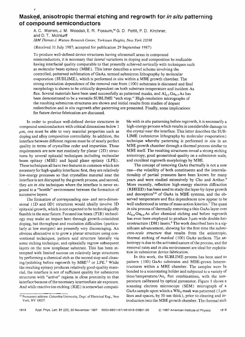
In this work, the SUBLIME process has been used to pattern (100) GaAs substrates and MBE-grown heterostructures within a MBE chamber. The samples were In bonded to a nonrotating holder and subjected to a variety of time/temperature/AS2 flux combinations, with the temperature calibrated by optical pyrometer. Figure 1 shows a scanning electron microscope (SEM) micrograph of a GaAs sample upon which a WSi2 mask was patterned ( 1j-lrn lines and spaces, by 50 nm thick), prior to cleaning and introduction into the MBE growth chamber. The thermal etch
1818 Appl. Phys. Lett. 51 (22),30 November 1987 0003-6951/87/481818-03$01.00 © 1987 American Institute of Physics 1818
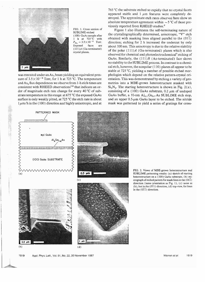
FIG. I. Cross section of SUBLIME-etched ( 1(0) GaAs sample after I h at 725'C with PA ., = 3.5X 10⁻⁶ Torr. Exposed faces are (III)A (Ga-terminated) crystal planes.
was executed under an AS2 beam yielding an equivalent pressure of 3.5 X 10⁻⁶ Torr, for 1 hat 725°C. The temperature and AS2 flux dependences we observe from 1-h etch times are consistent with RHEED observations5
.6 that indicate an or
der of magnitude etch rate change for every 40°C of substrate temperature in this range: at 675°C the exposed GaAs surface is only weakly pitted, at 725 ·C the etch rate is about 1j.Lmlh in the (100) direction and highly anisotropic, and at
epi GoAs
(d)
(c)
(100) GaAs SUBSTRATE
Appl. Phys. Lett., Vol. 51, No. 22, 30 November 1987
AlxGol_xAs
"""""""""".,.,.,.,.,.,.,..."""""""",:,"""{;;"';,:,"""";".,',.,.:,;"";,;",,:,"'~;";,;,:",,,:,.,
PATTERNED MASK
~L
(a)
(b)
1819
765 ·C the substrate etched so rapidly that no crystal facets appeared stable and 1 /-lm features were completely destroyed. The approximate etch rates observed here show an absolute temperature agreement within - 5 °C of those previously reported from RHEED studies. 6
Figure I also illustrates the self-terminating nature of the crystallographically determined, anisotropic, "V" etch obtained with masking lines aligned parallel to the (all) direction; etching for 2 h increased the undercut by only about 100 nm. This anisotropy is due to the relative stability of the polar (Ill)A (Ga-terminated) planes which is also observed for chemical and photoelectrochemical9 et~hing of GaAs. Similarly, the (111)B (As-terminated) face shows no stability to the SUBLIME process. In contrast to a chemical etch, however, the nonpolar (110) planes all appear to be stable at 725 ·C, yielding a number of possible etched morphologies which depend on the relative pattern-crystal orientation. This was demonstrated by etching a variety of geometries into a MBE-grown heterostructure masked with Si3N4 . The starting heterostructure is shown in Fig. 2(a), consisting of a (100) GaAs substrate, 0.2 /-lm of undoped GaAs buffer, a lO-nm Alo.3 Gao.? As SUBLIME etch stop, and an upper 0.5-j.Lm GaAs layer to be etched. The nitride mask was patterned to yield a series of gratings for cross-
FIG. 2. Views of MBE-grown heterostructure and SUBLIME patterning results: (a) sketch of starting heterostructure on a (100) GaAs substrate, (b) micrograph ofetched pattern for mask lines in the (011) direction (same orientation as Fig. 1), (c) same as (b), but in the (011) direction, (d) top view, for lines in the (oTI) direction.
Warren et 81. 1819

section studies and a variety of arbitrary shapes for top view of the resulting morphology. The Alo.) Gao.7 As etch stop was found to be fairly stable at 700 ·C as long as the AS2 flux was kept above -7X 10- 6 Torr, and results for (OIl) oriented nitride lines are shown in Fig. 2(b). The stability of the vertical (011) planes is il1ustrated by etching between nitride lines paral1el to the (01 I) direction as shown in Fig. 2(c), while etching lines oriented at 45· [(01) direction] exposed the various angled (110) faces seen from the top in Fig. 2 (d). The slight right-left anisotropies observed in the cross-section micrographs have been correlated with the incident beam direction and the etch-rate dependence upon AS2 flux, and should be eliminated with the use of a rotating substrate holder.
The Alo.) Gao.7 As etch-stop instability in the absence of sufficient AS2 flux, along with an AS2 beam shadowing produced by the combination of vertical sidewalls and slight undercutting shown in Fig. 2(b), has been used to produce some remarkable trench structures such as that shown in Fig. 3. This micrograph illustrates again the strong anisotropy of the SUBLIME process, and also demonstrates that thin Ala.) Gao 7As layers may either be used as an etch stop or etched completely through using SUBLIME, while higher Al composition layers provide less versatility. The cleanest results appear to be achieved by adjusting the AS2 flux to maximize the etch rate (up to about 1 /-lm/h) while still maintaining whatever Alx Gal _ x As stability is necessary.
In addition to studying the possible geometric structures that 'can be achieved, we have begun to look at the morphology of in situ MBE regrowth over SUBLIME-patterned substrates and at the redistribution of dopant atoms produced by the SUBLIME patterning technique. Typical, in situ regrowth morphology is illustrated in the SEM micrograph of Fig. 4, where the "substrate" was the V-groove structure shown in Fig. 1. One micron ofundoped GaAs was regrown with 10 nm Ala.3 Gao.7As markers inserted every 100 nm. The markers were then etched in buffered HF to delineate the regrowth contours. Initial results indicate that regrowth within such grooves yields roughly planar epitaxy (for a substrate temperature of 670 ·C), while the GaAs deposited on the SUBLIME mask is large-grain polycrystalline material. Initial photoelectrochemical C- V profiling through a planar SUBLIME/regrowth interface, where the
FIG. 3. Cross-section micrograph of trench structure produced by etching lines as in Fig. 2(c), but with AS2 flux incident from upper left. Beam shadowing results in localized etching through the lO-nm AIo. 3 Gao 7As etch stop adjacent to the patterned feature, and resulting trench formation.
FIG. 4. Cross section showing results of in situ regrowth over SUBLIME-patterned, Vgroove structure shown in Fig. I. Regrowth was of 1pm of GaAs with 10 nm AIo.3 Gao 7As contour markers every 100 nm. Material deposited on the WSi2 mask is large-grain polycrystalline GaAs.
initial and regrown layers were Si doped, confirms that nonvolatile dopants such as Si are not removed during SUBLIME; instead they pile up at the moving interface to produce an effective "delta doping." 10 It is expected that this can be avoided, if desired, by using volatile dopants such as Mg. Further details concerning dopant redistribution and regrowth over patterned heterostructures such as those shown in Fig. 2 will be presented elsewhere. It should be noted, however, that the dopant redistribution is detected through the carriers produced, and that the observed accumulation (rather than depletion) indicates not only that the "piled-up" dopants are largely activated, but also that the interface is not "pinned" by a large density of interface states. The unpinned state of this interface is an important result if the SUBLIME process is to be used for device fabrication.
From initial results shown here, several general observations may be made. First, it is clear that the SUBLIME process fulfills the basic requirements for the formation of highquality lateral interfaces necessary for good ultrasmall devices: it is both an in situ and low-energy patterning technique. It is also obvious that this process should be extendable to other volatile compound semiconductors such as Inx Gal _ x As. And while it has not yet been determined what the ultimate interface quality can be using SUBLIME, results pres'ented here suggest that virtually all GaAs-based devices could benefit from application of this technique.
'w. T. Tsang and A. Y. Cho, App!. Phys. Lett. 30, 293 (1977). 2J. S. Smith, P. L. Derry, S. Margalit, and A. Yariv, App!. Phys. Lett. 47, 712 (1985).
3D. Boetz, W. T. Tsang, and S. Wang, App!. Phys. Lett. 28, 234 (1976). 4A. Y. Cho and J. R. Arthur, Prog. Solid State Chern. 10,157 (1975). ST. Kojima, N. J. Kawai, T. Nakagawa, K. Ohta, T. Sakamoto, and M. Kawashima, App!. Phys. Lett. 47, 286 (1985).
6J. M. van Hove and P. 1. Cohen, App!. Phys. Lett. 47, 726 (1985). 7R. Heckingbottom, J. Vac. Sci. Techno!. B 3,572 (1985). 8H. Tanaka, M. Mushiage, Y. Ishida, and H. Fukada, Jpn. J. App!. Phys. 24, L89 (1985).
9M. M. Carrabba, N. M. Nguyen, and R. D. Rauh, J. Electrochem. Soc. Solid State Sci. Techno!. 134, 1855 (1987).
1Oe. E. e. Wood, G. M. Metze, J. D. Berry, and L. F. Eastman, J. App!. Phys. 51, 383 (1980).
1820 AppJ. Phys. Lett., Vol. 51, No. 22, 30 November 1987 Warren et al. 1820