master thesismaster thesis 2012 interface-state density of three dimensional silicon channels...
TRANSCRIPT

Master thesis 2012
Interface-state density of
three dimensional silicon channels measured by charge pumping method
Supervisor:
Professor Nobuyuki Sugii and Hiroshi Iwai
Department of Electronics and Applied Physics
Interdisciplinary Graduate School of Science and Engineering
Tokyo Institute of Technology
Student ID : 10M36356
Kazuhiro Nakajima
Abstract
Recently, multi-gate and nanowire field-effect-transistors (FETs) with
three-dimensional (3D) channels have drawing much interest because they have
excellent short-channel-effect immunity due to better electrostatic control of the
channel potential by gate electrodes. Therefore, the metal-oxide-semiconductor (MOS)
transistor with 3D channels has been considered as one of the promising candidates to
overcome the scaling issues in planar FETs.
Generally, the 3D channels formed by plasma etching and/or oxidation process are
consisted of various crystallographic orientations: facets or rounding shapes. One of
the concerns with these structures is the interface-state density (Dit), which is strongly
dependent on the surface orientations. Therefore, a direct measurement of
cross-sectional-shape dependent Dit and its distribution in energy band gap (Eg) is
required.
In this study, the interface-state density of 3D Si body with rectangular cross section
was measured by charge-pumping method with gated PIN diodes formed on a
silicon-on-insulator (SOI) wafer.
The PIN diodes were fabricated on line structures (fins) ranging from 70 to 110 nm
in width and a (100)-oriented planar SOI layer of 70 nm thick as a control.
14-nm-thick gate-oxide film was formed by dry oxidation at 1000oC for 10 min. P
and BF2 ions were implanted to form N+ and P+ regions, respectively, each adjacent to
the gate electrode. A tungsten (W) film was deposited by rf magnetron sputtering,
followed by the formation of the gate electrode by wet etching. Then, samples were
subjected to the activation annealing in nitrogen gas ambient at 800oC for 5 min.

Finally, the sample was annealed in forming gas (F.G.) (N2 : H2 = 97 : 3) ambient at 300
to 600oC for 30 min.
The interface-state density of the planar SOI structure was almost independent on
the channel length and width.
F.G. annealing temperature dependence was investigated for the 3D Si structures.
With increasing the F.G. annealing temperature from 300 to 420oC, the interface-state
density decreased gradually, especially at near the midgap. Further, with increasing the
forming gas annealing temperature from 420 to 540oC, the interface-state density, on
the contrary, increased gradually. The fin structures had higher Dit value than the planar
SOI in the entire energy range in the gap. Moreover, the increase in Dit with decreasing
the width of fin structures was found. From the fin-width dependency, Dit values of 1.3
x 1010 and 2.6 x 1011 cm-2 eV-1 for top and side surfaces were extracted, respectively.
It can be modeled that Dit can be estimated by the averaged Dit values of top and
sidewall surface areas, in proportion to the channel width.

CONTENTS
Chapter 1
Introduction 1.1 Background of this study 1.2 Scaling theory 1.3 CMOS Scaling limits 1.4 Multi gate FET 1.4.1 Planar double gate FET
1.4.2 Fin FET 1.4.3 Tri gate FET 1.4.4 Si nanowire FET
1.5 Issue in Three dimensional Si MOSFET 1.5.1 Interface state density
1.6 Purpose of this study References
Chapter 2
Fabrication and Characterization Method 2.1 Experimental procedure 2.2 Experimental details and principles 2.2.1 Fabrication of Fin-structures substrates 2.2.2 Substrate cleaning
2.2.3 Photolithography 2.2.4 Dry etching by RIE 2.2.5 Thermal oxidation 2.2.6 Ion implantation 2.2.7 RF magnetron sputtering
2.2.8 Wet etching with H2O2, HCl and BHF 2.2.9 Thermal evaporation of metal electrodes 2.2.10 Activation annealing and F.G. annealing
2.3 Characterization 2.3.1 Scanning Electron Microscope (SEM) 2.3.2 Charge pumping method
2.3.3 MOSFET Subthreshold Current Method References
Chapter 3
Interface-state density of 3D structure
3.1 Results and Discussion for planar SOI structures
3.1.1 Charge-pumping current 3.1.2 Energy distribution of Dit
3.2 Results and Discussion for 3D structures 3.2.1 Charge-pumping current 3.2.2 F.G. Annealing temperature dependence of Dit 3.2.3 Wfin dependence of Dit 3.3 Summary of this section References
Chapter 4
Geometric separation of Dit from top, side and
corner surfaces 4.1 Geometric separation of Dit from top and side surfaces
4.1.1 Model of Dit by the top and sides for geometric separation 4.1.2 Separation of Dit from top and side surfaces 4.2 Geometric separation of Dit from top, side and corners surfaces
4.2.1 Model of Dit by the top, sides and corners for geometric separation 4.2.2 Separation of Dit from top, side and corners 4.3 Summary of this section References

Chapter 5
Conclusion of This Study 5.1 Conclusion
Acknowledgments

1
Chapter1 Introduction 1.1 Background of this study
1.2 Scaling theory
1.3 CMOS scaling limits
1.3.1 Short Channel Effects
1.4 Multi gate FET
1.4.1 Planar double gate FET
1.4.2 Fin FET
1.4.3 Tri gate FET
1.4.4 Si nanowire FET
1.5 Issues in Three dimensional Si MOSFET
1.5.1 Interface-state density
1.6 Purpose of this study
References

2
1.1 Background of This Study In a modern highly-networked information society, complementary metal oxide
semiconductor (CMOS) ultra large scale integration (ULSI) is used for every product
as well as electronic equipment. The semiconductor industry is one of the key
industries to support society. The comfortable society realization is unthinkable
without the use of ULSI today.
The ULSI is constructed mostly of a number of metal-oxide-semiconductor
field-effect transistors (MOSFETs). The progress of ULSI circuits such as
improvement of the processing speed of information, recording large-capacity
information, reduction of electrical power consumption and cost reduction have been
made by the device scaling of MOSFETs [1.1]. After aggressive downsizing the
MOSFETs, the size of planar FET has reached down to 30 nm and it becomes difficult
to further decrease the size.
Recently, multi-gate and nanowire FETs with three-dimensional (3D) channels
have drawing much interest because they have excellent short-channel-effect immunity
due to better electrostatic control of the channel potential by gate electrodes. Therefore,
by employing MOSFET with 3D channels, ULSI circuits can be further improved
[1.2-3].

3
1.2 Scaling theory ULSI circuits have been developed by continuous miniaturization based on the
scaling theory. In 1974, Dennard et al. proposed the constant-field scaling theory [1.4].
Table 1.1 shows parameters in the constant-field scaling.
Table 1.1 MOSFET scaling rules.
1Power density (P)
1/k2Power dissipation per circuit
1/kCircuit delay time (t)
1/k2Device area
1/kGate capacitance (Cox)
1/kCurrent (I)
1/kVoltage (V)
1/kDoping concentration (Na)
1/kGate oxide thickness (tox)
1/kChannel width (W)
1/kChannel length (L)
Scaling FactorParameters
1Power density (P)
1/k2Power dissipation per circuit
1/kCircuit delay time (t)
1/k2Device area
1/kGate capacitance (Cox)
1/kCurrent (I)
1/kVoltage (V)
1/kDoping concentration (Na)
1/kGate oxide thickness (tox)
1/kChannel width (W)
1/kChannel length (L)
Scaling FactorParameters

4
1.3 CMOS scaling limits Planar transistors have been the core of integrated circuits for several decades,
during which the size of the individual transistors has steadily decreased. MOSFET
performance can be basically improved by downsizing. After aggressive downsizing
the FETs, the feature size of state-of-the-art FETs has reached less than 30 nm. As the
size decreases, planar transistors increasingly suffer from the undesirable short-channel
effects (SCEs), especially increase in the "off-state" leakage current, which increases
the idle power of the LSI chip [1.5].
1.3.1 Short-Channel Effects
A MOSFET device is considered to be in the “short-channel” regime that the
so-called short-channel effect significantly degrades the transistor performance when
the channel length is the same order of magnitude as the depletion-layer widths of the
source and drain junction. As the channel length (L) is reduced to increase both the
operation speed and the number of components per chip, the depletion width should be
decreased in the conventional bulk MOSFETs. However, this has become very
difficult in the recent generations [1.6].
1.4 Multi gate FET In a multi-gate device, the channel is surrounded by several gates on multiple
surfaces, allowing more effective suppression of "off-state" leakage current. The
multi-gate devices also allow enhanced current per area in the "on-state”. These
advantages translate into lower leakage power consumption and enhanced device

5
performance. Nonplanar devices are also more compact than the conventional planar
transistors, enabling higher transistor density which translates to smaller chip size.
Moreover, a wide variety of multiple gate architectures have been proposed and
demonstrated: planar double-gate, Fin FET, Tri-gate and Gate-All-Around (GAA), Si
nanowire FET etc. Figure 1.1 shows schematic illustrations of the multi-gate Si FETs.
Si Sub.BOX
Wfin
Gate
Drain
Source
Lg
Hfin
Gate
S Channel n+ D
Gate
n+
Lg
Wg
Planar double-gate FET Fin FET Si nanowire FET
Source
GateDrain Si nanowire
Si Sub.BOX
Lg
Figure 1.1 Multi gate device structures.
1.4.1 Planar double-gate FET
Planar double-gate transistors employ conventional planar (layer by layer)
manufacturing processes to create double-gate devices, avoiding more stringent
fabrication process requirements associated with non-planar transistor structures. In the
planar double-gate transistors, the silicon body (channel) is sandwiched between two
independently fabricated gate/gate oxide stacks. The primary challenge in fabricating
such structures is achieving satisfactory self-alignment between the upper and lower
gates [1.7].

6
n+
Gate
Gate
n+ Channel DS
Lg
Figure 1.2 Cross-sectional schematic illustration of planar double-gate FET.
1.4.2 Fin FET
Even though current conduction is in the surface of the wafer, it is not strictly a
planar device. Rather, it is referred to as a quasi-planar device, because its geometry in
the vertical direction (that is the fin height) also affects the device performance.
Amongst the double gate FET types, the FinFET is the easiest one to fabricate [1.8-10].
The original form of the FinFET is the “DELTA” structure [11] The Fin FET consists
of a vertical Si fin controlled by self-aligned double-gate.
Si Sub.BOX
ChannelGate
Hard Mask
Wfin
Hfin
Figure 1.3 Cross-sectional schematic illustration of Fin FET
1.4.3 Tri-gate FET
The Tri-Gate design is essentially a variant of the 'Fin FET' 3D structure[*].
In the three-dimensional tri-gate transistor, there's multiple gate surfaces in contact
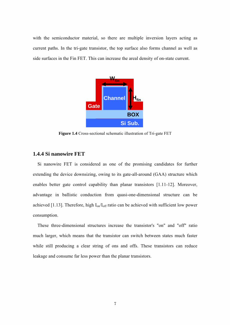
7
with the semiconductor material, so there are multiple inversion layers acting as
current paths. In the tri-gate transistor, the top surface also forms channel as well as
side surfaces in the Fin FET. This can increase the areal density of on-state current.
Si Sub.BOX
ChannelGate
Wfin
Hfin
Figure 1.4 Cross-sectional schematic illustration of Tri-gate FET
1.4.4 Si nanowire FET
Si nanowire FET is considered as one of the promising candidates for further
extending the device downsizing, owing to its gate-all-around (GAA) structure which
enables better gate control capability than planar transistors [1.11-12]. Moreover,
advantage in ballistic conduction from quasi-one-dimensional structure can be
achieved [1.13]. Therefore, high Ion/Ioff ratio can be achieved with sufficient low power
consumption.
These three-dimensional structures increase the transistor's "on" and "off" ratio
much larger, which means that the transistor can switch between states much faster
while still producing a clear string of ons and offs. These transistors can reduce
leakage and consume far less power than the planar transistors.

8
Si Sub.BOX
Gate
Si nanowire
Channel
Insulator
Gate
Figure 1.5 Cross-sectional schematic illustration of Si nanowire FET
1.5 Issues in Three dimensional Si MOSFET
Generally, the 3D channels are fabricated by plasma etching and subsequent
oxidation processes. Therefore, the surface of the 3D channel may consist of various
crystallographic orientations: facets or rounding shapes.
As shown in Figure 1.6, the top surface is (100) and the sidewall is (110). One of the
concerns is the increase in interface-state density (Dit) caused by increasing the portion
of high-index planes, that is considered to have higher Dit, with decreasing the size.
The interface-state density is strongly dependent on surface orientations [1.2-3].
Figures 1.6 Schematics of interface-state density of 3D channel.
Wfin
BOXSub.
Hfin
(100)(110) Gate

9
1.5.1 Interface-state density
The silicon atom possesses four valence electrons and therefore requires four bonds
to fully saturate (fill?) the valence shell. In the crystalline structure each silicon atom
establishes bonds to its four neighboring atoms, leaving no dangling bond behind. At
the surface of the silicon crystal atoms are missing counterparts to bond and dangling
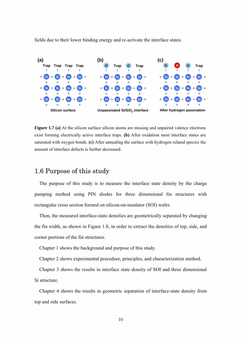
bonds that become trap centers are formed as shown in Figure 1.7 (a). The density of
these interface states, Dit, in this regime is approximately Dit ≈ 1014 cm-2 eV-1. After
oxidation most of suraface bonds are connected with oxygen atoms (Figure 1.7(b)).
The density then reduces to approximately Dit ≈ 1012 cm-2 eV-1 [1.14].
This number is already a small as the interface-state density of semiconductor
suraface thanks to the good combination of silicon and silicon dioxide. But in an MOS
transistor with a gate length of 100 nm and a gate width of 1µm this density still
translates to 1000 dangling bonds in the active area. With such a high number of
interface defects a transistor would still not operate properly. Therefore, it is mandatory
to increase the quality of the Si/SiO2 interface in MOS device technology as much as
possible. Each electrically active interface-state leads to a degradation of important
transistor parameters such as the threshold voltage, the on-current, or the surface
carrier mobility. To further improve the interface quality, the number of dangling bonds
should be further reduced by annealing the interface in forming gas with hydrogen
molecules, as shown in Figure 1.7 (c). The dangling silicon bonds are passivated by
forming Si-H bonds. With this treatment the amount of electrically active interface
states can be reduced to around Dit ≈ 1010 cm-2 eV-1.
This is an acceptable number and a first-class Si/SiO2 interface can be formed.
Ironically, exactly these Si-H bonds are the cause for negative bias temperature
instability (NBTI). The bonds can break at elevated temperatures and high electric
10
fields due to their lower binding energy and re-activate the interface states.
Si= Si= =Si= Si =
= = = =
Si= Si= =Si= Si =
= = = =
Si= Si= =Si= Si =
= = = =
Trap Trap Trap Trap
Silicon surface
Si= Si= =Si= Si == = = =
Si= Si= =Si= Si =
= = = =
Si= Si= =Si= Si =
= = = =
Trap
After hydrogen passivation
O OH
Si= Si= =Si= Si =
= = = =
Si= Si= =Si= Si =
= = = =Si= Si= =Si= Si =
= = = =
Trap Trap
Unpassivated Si/SiO2 interface
O O(a) (b) (c)
Figure 1.7 (a) At the silicon surface silicon atoms are missing and unpaired valence electrons exist forming electrically active interface traps. (b) After oxidation most interface states are saturated with oxygen bonds. (c) After annealing the surface with hydrogen related species the amount of interface defects is further decreased.
1.6 Purpose of this study
The purpose of this study is to measure the interface state density by the charge
pumping method using PIN diodes for three dimensional fin structures with
rectangular cross section formed on silicon-on-insulator (SOI) wafer.
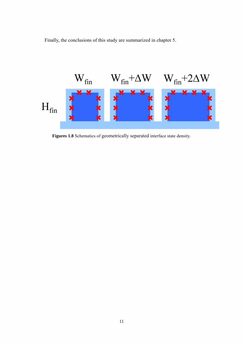
Then, the measured interface-state densities are geometrically separated by changing
the fin width, as shown in Figure 1.8, in order to extract the densities of top, side, and
corner portions of the fin structures.
Chapter 1 shows the background and purpose of this study.
Chapter 2 shows experimental procedure, principles, and characterization method.
Chapter 3 shows the results in interface state density of SOI and three dimensional
Si structure.
Chapter 4 shows the results in geometric separation of interface-state density from
top and side surfaces.
11
Finally, the conclusions of this study are summarized in chapter 5.
Hfin
Wfin Wfin+∆W Wfin+2∆W
Figures 1.8 Schematics of geometrically separated interface state density.
12
References [1.1] H. Iwai. CMOS technology –year 2010 and beyond., IEEE J. Solid-State Circuits.
34, (1999), pp. 357.
[1.2] F.-L.Yang, D-H.Lee, H-Y.Chen, C-Y.Chang, S-D.Liu, C-C.Huang, T-X.Chung,
H-W.Chen, C-C.Huang, Y-H.Liu, C-C.Wu, C-C.Chen, S-C.Chen, Y-T.Chen, Y-H.Chen,
C-l.Chen, B-W.Chan, P-F.Hsu, J-H.Shieh, H-J.Tao, Y-C.YEO, Y.Li, l-W.Lee, P.Chen,
M-S.Liang,C.Hu, 5nm-Gate Nanowire FinFET, Symp. VLSI on Tech., (2004), pp.
196-197.
[1.3] L.Mathew, M.Sadd, S.Kalpat, M.Zavala, T.Stephens, R.Mora, S.Bagchi, C.Parker,
J.Vasek, D.Sing, R.Shimer, L.Prabhu, G.O.Workman, G.Ablen, Z.Shi, J.Saenz, B.Min,
D.Burnett, B-Y.Nguyen, J.Mogab, M.M.Chowdhury, W.Zhang, J.G.Fossum, Inverted T
channel FET (ITFET) – Fabrication and Characteristics of Vertical-Horizontal, Thin
Body , Multi-Gate , Multi-Orientation Devices, ITFET SRAM Bit-cell operation. A
Novel Technology for 45nm and Beyond CMOS. Tech. Dig. of IEDM, (2005), pp.
713-716.
[1.4] R. H. Dennard, F. H. Gaensslen, H. N. Yu, V. L. Rideout, E. Bassous, and A. R.
Le Blanc. Design of ion-implanted MOSFETs with very small physical dimensions.,
IEEE. J. Solid-State Circuits, 9, (1974), pp. 256.
[1.5] Subramanian.V., Multiple gate field-effect transistors for future CMOS
technologies, IETE Technical Review, 27, (2010), pp.446–454.
[1.6] F.D’Agostino, D.Quercia. Short-Channel Effects in MOSFETs, (2000)
[1.7] Wong.H-S, Chan.K, Taur.Y, Self-Aligned (Top and Bottom) Double-Gate
MOSFET with a 25 nm Thick Silicon Channel, IEDM, (1997), pp.427

13
[1.8] D.Hisamoto, T.Kaga, E.Takeda, Impact of the vertical SOI 'Delta' Structure on
Planar Device Technology, IEEE Trans. Electron Devices. 38, (1991), pp. 1419-1424.
[1.9] X.Huang, W-C.Lee, C.Kuo, D.Hisamoto, L.Chang, J.Kedzierski, E.Anderson, H.
Takeuchi, Y-K.Choi, K.Asano, V.Subramanian, T-J.King, J.Bokor, C.Hu, Sub 50-nm
FinFET: PMOS, International Electron Devices Meeting Technical Digest, (1999), pp.
67.
[1.10] X.Huang, W-C.Lee, C.Kuo, D.Hisamoto, L.Chang, J.Kedzierski, E.Anderson, H.
Takeuchi, Y-K.Choi, K.Asano, V.Subramanian, T-J.King, J.Bokor, C.Hu, Sub-50 nm
P-channel FinFET, IEEE Trans. Electron. 48, (2001), pp. 880
[1.11] S.D.Suk, S-Y.Lee, S-M.Kim, E-J.Yoon, M-S.Kim, M.Li, C.W.Oh, K.H.Yeo, S.
H. Kim, D-S.Shin, K-H.Lee, H.S.Park, J.N.Han,C.J.Park, J-B.Park, D-W.Kim, D.Park,
B-I.Ryu., High Performance 5nm radius Twin Silicon Nanowire MOSFET
(TSNWFET): Fabrication on Bulk Si Wafer, Characteristics, and Reliability, Tech. Dig.
of IEDM, (2005), pp.717- 720
[1.12] K.H.Cho, S.D.Suk, Y.Y.Yeoh, M.Li, K.H.Yeo, D-W.Kim, S.W.Hwang, D.Park,
B-I. Ryu, Gate-All-Around (GAA) Twin Silicon Nanowire MOSFET (TSNWFET)
with 15 nm Length Gate and 4 nm Radius Nanowires, Tech. Dig. of IEDM, (2006), pp.
1- 4.
[1.13] N.Singh, A.Agarwal, L.K.Bera, T.Y.Liow, R.Yang, S.C.Rustagi, C.H.Tung,
R.Kumar, G.Q.Lo, N.Balasubramanian, D.-L.Kwong, High-Performance fully depleted
Silicon Nanowire Gate-All-Around CMOS devices, IEEE Electron Device Letters, 27,
(2006), pp.383–386.
[1.14] A.H.Edwards, Interaction of H and H2 with the Silicon Dangling Orbital at the
<111> Si/SiO2 Interface, Phys.Rev.B, 44, (1991), pp. 1832-1838.

14
Chapter2 Fabrication and Characterization Method 2.1 Experimental procedure
2.2 Experimental details and principles
2.2.1 Fabrication of Fin-structures
2.2.2 Substrate cleaning
2.2.3 Photolithography
2.2.4 Dry etching by RIE
2.2.5 Thermal oxidation
2.2.6 Ion implantation
2.2.7 RF magnetron-sputtering
2.2.8 Wet etching with H2O2, HCl and BHF
2.2.9 Thermal evaporation
2.2.10 Activation annealing and F.G. annealing
2.3 Measurement methods
2.3.1 Scanning Electron Microscope (SEM)
2.3.2 Charge pumping method
References
15
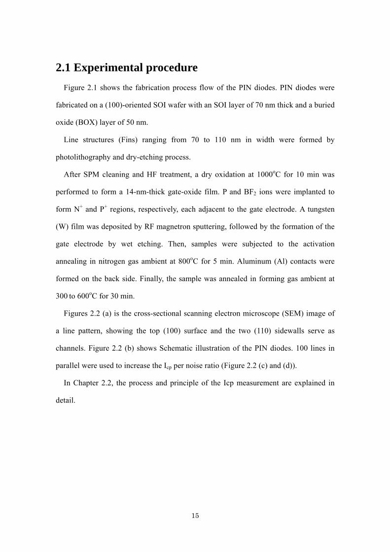
2.1 Experimental procedure Figure 2.1 shows the fabrication process flow of the PIN diodes. PIN diodes were
fabricated on a (100)-oriented SOI wafer with an SOI layer of 70 nm thick and a buried
oxide (BOX) layer of 50 nm.
Line structures (Fins) ranging from 70 to 110 nm in width were formed by
photolithography and dry-etching process.
After SPM cleaning and HF treatment, a dry oxidation at 1000oC for 10 min was
performed to form a 14-nm-thick gate-oxide film. P and BF2 ions were implanted to
form N+ and P+ regions, respectively, each adjacent to the gate electrode. A tungsten
(W) film was deposited by RF magnetron sputtering, followed by the formation of the
gate electrode by wet etching. Then, samples were subjected to the activation
annealing in nitrogen gas ambient at 800oC for 5 min. Aluminum (Al) contacts were
formed on the back side. Finally, the sample was annealed in forming gas ambient at
300 to 600oC for 30 min.
Figures 2.2 (a) is the cross-sectional scanning electron microscope (SEM) image of
a line pattern, showing the top (100) surface and the two (110) sidewalls serve as
channels. Figure 2.2 (b) shows Schematic illustration of the PIN diodes. 100 lines in
parallel were used to increase the Icp per noise ratio (Figure 2.2 (c) and (d)).
In Chapter 2.2, the process and principle of the Icp measurement are explained in
detail.
16
Fin Patterning by photolithography and dry-etchingStarting wafer:p type 140ohm-cmSOI wafer (100)-orientedSOI layer (70nm) / BOX layer (50nm)
Substrate cleaning (SPM+HF)
Gate oxide film formation by a dry oxidation at 1000 oC for 10min.
P ion implantation (Phosphorus , 30keV, 3×1014 cm-2)
BF2 ion implantation (Boron , 30keV, 3×1014 cm-2)
W film deposition by RF sputtering
Activation annealing in N2 gas ambient at 800 oC for 5 min.
Al back side contact deposition by thermal evaporation
Annealing in F.G. ambient at 300 to 600 oC by 20 oC steps for 30 min.
PIN gated diode
Si Sub.BOX
SiO2
Si Sub.BOXN+
Resist pattern
Si Sub.BOX
P+N+
Si Sub.BOX
WP+N+
Al
Si Sub.BOX
WP+N+
Si Sub.BOX
Figure 2.1 Fabrication process flow of PIN diodes.
Sub.BOX
W Gate SiO2
Sub.
N+ P+
BOX Leff
100 lines
BOX
N+ P+
WWfin= 70-110 nm
BOXSub.
Hfin=70(nm)(100)(110)
Si
BOX 50nm
Hfin70nm
Wfin80nm
W
100nm
(a) (b)
(c) (d)
Figure 2.2 (a) SEM image of a Fin structure. (b) Schematic illustration of the PIN diodes. (c)(d)
Fin structures with a number of 100 are used to ease the measurement of Icp.

17
2.2 Experimental details and principle
2.2.1 Fabrication of Fin-structures substrate
Narrow Si Line structures (Fins) ranging from 70 to 110 nm in width were fabricated
on a (100)-oriented SOI wafer with an SOI layer of 70 nm thick and a BOX layer of 50
nm thick by photolithography and dry-etching process (Figure 2.3). The direction of
the Fin structures was aligned to <110>.
Photolithography and
dry-etching process Si Sub.BOXSOI
30nm70nm
Si Sub.BOX
Wfin= 70-110nm
Figure 2.3 Schematic illustration of Si Fin structures
2.2.2 Substrate cleaning
At first, the experiments using high quality thin films require ultra clean surface of
Si fin structures without particle contamination, metal contamination, organic
contamination, ionic contamination, native oxide and atomic scale roughness.
One of the most important chemicals used in Si substrate cleaning is DI (de-ionized)
water. DI water is highly purified and filtered to remove all traces of ionic, particulate,
and bacterial contamination. The theoretical resistivity of pure water is 18.25 MΩ・cm
at 25oC. Ultra-pure water (UPW) system used in this study provided UPW of more
than 18.2 MΩ・cm at resistivity, fewer than 1 colony of bacteria per milliliter and fewer
than 1 particle per milliliter.
In this study, the Si substrate was cleaned on a basis of RCA cleaning process,
which was proposed by W. Kern et al. But some steps were omitted. The first step,

18
which use a solution of sulfuric acid (H2SO4) and hydrogen peroxide (H2O2) (H2SO4 :
H2O2 = 4 : 1), was performed to remove any organic material and metallic impurities.
After dipping in the the solution to clean the substrate, the wafer was dipped in DI
water to rinse away the chemicals. The process dipping the wafer in DI water after
dipping the wafer in chemicals with each cycle is important. Then, the native or
chemical oxide was removed by 1% diluted hydrofluoric acid (HF) (Figure 2.4).
Finally, the cleaned substrate was loaded to the oxidation chamber to deposit
immediately after it was dried by air gun.
Si Sub.BOX
Si Sub.BOX
Metal ion ParticleChemical Oxide
Si Sub.BOX
SPM HF
Figure 2.4 Schematic illustration of Substrate cleaning process.
2.2.3 Photolithography
Photolithography (or "optical lithography") is a process used in microfabrication to
selectively remove parts of a thin film or the bulk of a substrate. It uses light to transfer
a geometric pattern from a photomask to a light-sensitive chemical "photoresist", or
simply "resist," on the substrate. A series of chemical treatments then either engraves
the exposure pattern into, or enables deposition of a new material in the desired pattern
upon, the material underneath the photoresist (Figure 2.5). It is used because it can
create extremely small patterns (down to a few tens of nanometers in size), it affords
exact control over the shape and size of the objects it creates.
In case of this study, photolithography was used for the method to etch only parts of
unwanted fin pattern, gate metal and contacts, and barrier of ion implantation process.
The process flow and a photo of the photolithography apparatus used throughout
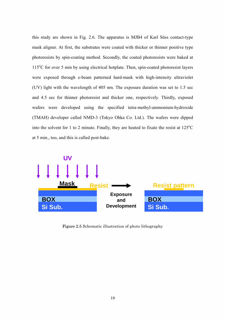
19
this study are shown in Fig. 2.6. The apparatus is MJB4 of Karl Süss contact-type
mask aligner. At first, the substrates were coated with thicker or thinner positive type
photoresists by spin-coating method. Secondly, the coated photoresists were baked at
115oC for over 5 min by using electrical hotplate. Then, spin-coated photoresist layers
were exposed through e-beam patterned hard-mask with high-intensity ultraviolet
(UV) light with the wavelength of 405 nm. The exposure duration was set to 1.5 sec
and 4.5 sec for thinner photoresist and thicker one, respectively. Thirdly, exposed
wafers were developed using the specified tetra-methyl-ammonium-hydroxide
(TMAH) developer called NMD-3 (Tokyo Ohka Co. Ltd.). The wafers were dipped
into the solvent for 1 to 2 minute. Finally, they are heated to fixate the resist at 125oC
at 5 min., too, and this is called post-bake.
Si Sub.BOX
ResistMask
UV
Si Sub.BOX
Resist patternExposure
and Development
Figure 2.5 Schematic illustration of photo lithography

20
1
23
4
5
Photoresist spin-coating
Pre-baking at 115oC for over 5 min.
Post-baking at 125oC for 5 min.
Exposure
Development
Figure 2.6 The process flow and the photo of photolithography apparatus.
2.2.4 Dry etching by RIE
After first photolithography, Reactive Ion Etching (RIE) was performed to eliminate
only parts of required Fin patterns. For etching of Si Fin, sulfur hexafluoride (SF6) is
used to etch in this study.
RIE is one of the methods to an etching technology [2.1]. It uses chemically
reactive plasma to remove material deposited on wafers. The plasma is generated
under low pressure (vacuum) by an electromagnetic field. High-energy ions from the
plasma attack the wafer surface and react with it.
2.2.5 Thermal oxidation process
The SiO2-covered Si fin structures were fabricated by thermal oxidation of the Si
substrate with preformed fin-structures on it. Thermal oxidation is accomplished by
using an oxidation furnace (or diffusion furnace, since oxidation is basically a
diffusion process involving oxidant species), which provides the heat needed to
elevate the oxidizing ambient temperature. A furnace typically consists of: 1) a

21
cabinet; 2) a heating system; 3) a temperature measurement and control system; 4)
fused quartz tubes where the wafers undergo oxidation; 5) a system which transfers
process gases into and out of the tubes; and 6) a loading station used for loading (or
unloading) wafers into (or from) the tubes.
The heating system usually consists of several heating elements that control the
temperature of the furnace tubes. The wafers are placed in quartz glassware known as
boats, which are supported by fused silica paddles inside the process tube. A boat
can support many wafers. The oxidizing agent (oxygen or steam) then enters the
process tube through its source end, subsequently diffusing to the wafers surface
where the oxidation occurs. In this study, the dry oxidation furnace shown in Fig. 2.5
was used.
Depending on oxidant species used (O2 or H2O), the thermal oxidation of SiO2 may
either be in the form of dry oxidation (wherein the oxidant is O2) or wet oxidation
(wherein the oxidant is H2O). The reactions for dry and wet oxidation are governed
by the following equations:
1) for dry oxidation: Si (solid) + O2 (gas) → SiO2 (solid); and
2) for wet oxidation: Si (solid) + 2H2O (gas) → SiO2 (solid) + 2H2 (gas).
Figure 2.6 shows the dry thermal oxidation rate using bulk p-Si substrate and SOI
substrate which has 51-nm-thick SOI, 137.8-nm-thick BOX layer. The figure indicates
that SiO2 thickness increases and residual SOI thickness decreases as increasing
oxidation time [2.2-3].
In this study, the thermal oxidation was performed by dry process at 1000oC for 10
min, which results in formations of Si channel covered by about 14-nm-thick SiO2.

22
Figure 2.5 Oxidation furnaces.
0
20
40
60
80
100
120
0 20 40 60 80 100 120 140 160 1800 20 40 60 80 100 120 140 160 1800
20
40
60
80
100
120
Oxidation Time (min)
Oxi
de a
nd S
OI T
hick
ness
(nm
)
Residual SOI Thickness
Oxide Thickness of SOI Substrate
Oxide Thickness of Bulk P-Si Substrate
Figure 2.6 Rate of dry oxidation.
23
2.2.6 Ion implantation
After a dry oxidation process, P and BF2 ions were implanted to form N+ and
P+ regions, respectively, each adjacent to the gate electrode.
Ion implantation equipment typically consists of an ion source, where ions of
the desired element are produced, an accelerator, where the ions are
electrostatically accelerated to a high energy, and a target chamber, where the ions
impinge on a target, which is the material to be implanted. Thus ion implantation
is a special case of particle radiation. Each ion is typically formed from a single
atom or molecule by removing single or multiple electrons, and thus the actual
amount of material implanted in the target is identical to the integrated value over
time of the ion current. This amount is called the dose. The currents supplied by
implanters are typically small (microamperes), and thus the dose which can be
implanted in a reasonable amount of time is small. Therefore, ion implantation
finds application in cases where the amount of chemical change required is small.
Dopant ions such as boron (B), phosphorus (P) or arsenic (As) are generally
created from a gas source, so that the purity of the source can be very high. Boron
trifluoride (BF3), phosphine (PH3) and arsine (AsH3) gases are generally used for
the B, P and As of the dopant atoms. These gases are very hazardous. When
implanted in a semiconductor, each dopant atom can create a charge in the
semiconductor after annealing. A hole can be created by a p-type dopant, and an
electron by an n-type dopant. The implanted ion is inert unless it is bonded with a
crystal lattice. Therefore, annealing process is necessary to fix damages in the
crystal lattice by heating after ion implantation.
Ion implantation was developed as a method of producing the PN junction of
photovoltaic devices in the late 1970s and early 1980s [2.4], along with the use of

24
pulsed-electron beam for rapid annealing [2.5], although it has not to date been
used for commercial production.
・
・
・
・
・
・
・・
・・
・
・
・
・
・
・・
・・
・
・
・
AIon source
Current integrator
Udesell
Uaesell
・
・
・
・
・
・
・・
・・
・
・
・
・
・
Substrate
Separation Magnet
Figure 2.7 Schematic illustration of Ion implanter
2.2.7 RF magnetron-sputtering
After twice ion implantation processes, a tungsten (W) film was deposited by
radio frequency (rf) magnetron sputtering.
The sputtering is one of the vacuum processes depositing thin films. A high
electric field across a low-pressure gas (usually argon at about 10 mTorr) is applied to
create a “plasma,” which consists of electrons and gas ions in a high-energy state. Then
the energized plasma ions strike the “target,” composed of the desired coating material,
and cause atoms of the target to be ejected with enough energy to travel to the substrate
surface.
In this study, W film with thickness of 50 nm was deposited on SiO2-coverd Si by
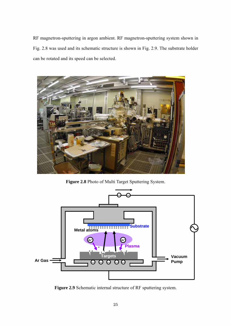
25
RF magnetron-sputtering in argon ambient. RF magnetron-sputtering system shown in
Fig. 2.8 was used and its schematic structure is shown in Fig. 2.9. The substrate holder
can be rotated and its speed can be selected.
Figure 2.8 Photo of Multi Target Sputtering System.
Plasma
Substrate
Targets
Metal atoms
Ar GasVacuum Pump- - - - -
- -
Ar+ Ar+
Figure 2.9 Schematic internal structure of RF sputtering system.
26
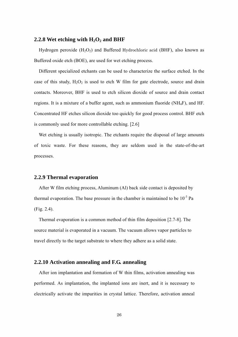
2.2.8 Wet etching with H2O2 and BHF
Hydrogen peroxide (H2O2) and Buffered Hydrochloric acid (BHF), also known as
Buffered oxide etch (BOE), are used for wet etching process.
Different specialized etchants can be used to characterize the surface etched. In the
case of this study, H2O2 is used to etch W film for gate electrode, source and drain
contacts. Moreover, BHF is used to etch silicon dioxide of source and drain contact
regions. It is a mixture of a buffer agent, such as ammonium fluoride (NH4F), and HF.
Concentrated HF etches silicon dioxide too quickly for good process control. BHF etch
is commonly used for more controllable etching. [2.6]
Wet etching is usually isotropic. The etchants require the disposal of large amounts
of toxic waste. For these reasons, they are seldom used in the state-of-the-art
processes.
2.2.9 Thermal evaporation
After W film etching process, Aluminum (Al) back side contact is deposited by
thermal evaporation. The base pressure in the chamber is maintained to be 10-3 Pa
(Fig. 2.4).
Thermal evaporation is a common method of thin film deposition [2.7-8]. The
source material is evaporated in a vacuum. The vacuum allows vapor particles to
travel directly to the target substrate to where they adhere as a solid state.
2.2.10 Activation annealing and F.G. annealing
After ion implantation and formation of W thin films, activation annealing was
performed. As implantation, the implanted ions are inert, and it is necessary to
electrically activate the impurities in crystal lattice. Therefore, activation anneal
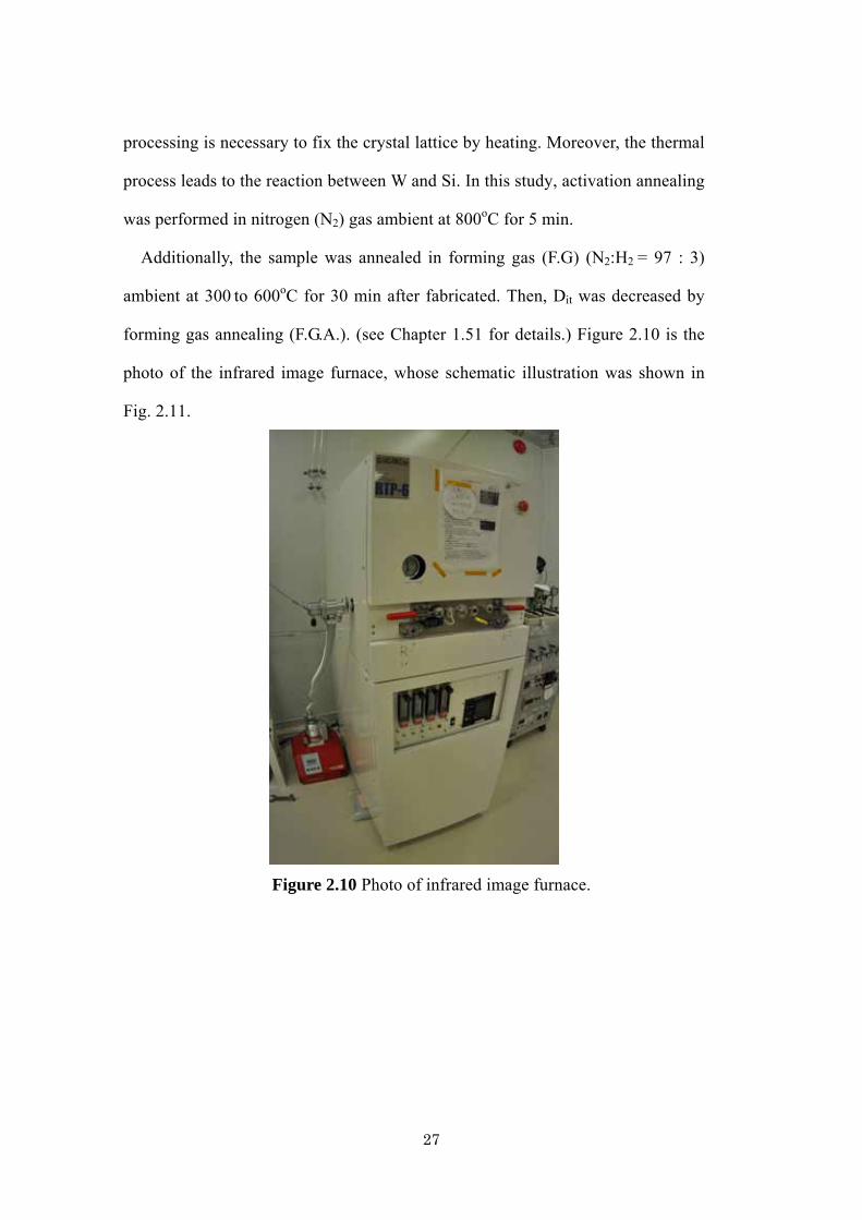
27
processing is necessary to fix the crystal lattice by heating. Moreover, the thermal
process leads to the reaction between W and Si. In this study, activation annealing
was performed in nitrogen (N2) gas ambient at 800oC for 5 min.
Additionally, the sample was annealed in forming gas (F.G) (N2:H2 = 97 : 3)
ambient at 300 to 600oC for 30 min after fabricated. Then, Dit was decreased by
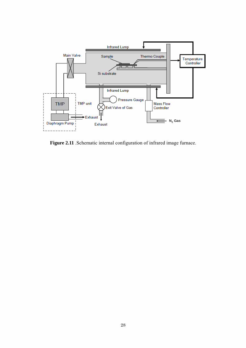
forming gas annealing (F.G.A.). (see Chapter 1.51 for details.) Figure 2.10 is the
photo of the infrared image furnace, whose schematic illustration was shown in
Fig. 2.11.
Figure 2.10 Photo of infrared image furnace.
28
N2 GasN2 Gas
Figure 2.11 .Schematic internal configuration of infrared image furnace.

29
2.3 Characterization Methods
2.3.1 Scanning Electron Microscope (SEM)
The formed 3D fin structures were microscopically observed in order to measure the
size of the Si channel area by scanning electron microscope (SEM). The observation
was mainly performed by overhead viewing.
Figure.2.12 shows Scanning Electron Microscope (SEM) system S-4800 (HITACHI
High-Technologies Corporation) and its schematic internal configuration is shown in
Fig. 2.13. The “Virtual Source” at the top represents the electron gun, producing a
beam of monochromatic electrons. The beam is condensed by the first condenser lens.
This lens is used to both form the beam and limit the amount of current in the beam. It
works in conjunction with the condenser aperture to cut off the high-angle electrons
into a thin, tight, coherent beam. A user selectable objective aperture further eliminates
high-angle electrons from the beam. A set of coils then scan or sweep the beam in a
grid fashion and make the beam dwell on points for a period of time determined by the
scan speed. The final lens, the objective, focuses the scanning beam onto the part of the
specimen desired. When the beam strikes the sample, interactions occur inside the
sample and are detected with various instruments interactions. Before the beam moves
to its next dwell point these instruments count the number of interactions and display a
pixel on a display whose intensity is determined by this number. This process is
repeated until the grid scan is finished and then repeated, the entire pattern can be
scanned 30 times per second.

30
Figure 2.12 Photograph of SEM equipment.
Virtual Source
First Condenser Lens
Condenser Aperture
Objective Aperture
Second Condenser Lens
Scan Coils
Objective Lens
Sample Figure 2.13 Schematic view of internal configuration of SEM equipment.

31
2.3.2 Characterization of Interfaces The excellent quality of the Si/SiO2 interface is one of the main reasons for the
success of the modern ULSI MOS technology. Therefore, it is very important to
characterize the quality of this interface as precisely as possible.
Table 2.1 shows classification of interface characterization techniques.
In this study, the charge pumping method was employed to measure the dependence
of Dit on size and shape of 3D structures.
As the fin structures were fabricated on an SOI wafer, the method of direct
measuring interface-state density is only the charge pumping method. Therefore,
charge pumping method was performed.
Table 2.1 Classification of interface characterization techniques
Charge pumping method
DC-IV
Current DLTSMOSFET subthresholdcurrent method
Transistor
DLTSHigh-Frequency method (Terman method)
Conductance method Low-Frequency method (Quasi static method)
Capacitance
Direct techniqueIndirect technique
Charge pumping method
DC-IV
Current DLTSMOSFET subthresholdcurrent method
Transistor
DLTSHigh-Frequency method (Terman method)
Conductance method Low-Frequency method (Quasi static method)
Capacitance
Direct techniqueIndirect technique

32
2.3.2.1 Charge Pumping Method
The charge pumping method has shown to be a very reliable and also precise method
allowing the in-depth analysis of the interface, directly in the MOSFET device.
Additionally it only requires basic equipment and is relatively easy to set up.
The effect has been first reported by Brugler and Jespers in 1969 [2.10]. They
reported a net dc substrate current when applying periodic pulses to the gate of a MOS
transistor, while keeping source and drain grounded. The current was found to be
proportional to the gate area and the frequency of the applied gate pulses. It was
flowing in the opposite direction of the leakage current of the source and drain to
substrate diodes. They showed that the current originates from recombination of
minority and majority carriers at traps at the Si/SiO2 interface. Therefore, the method
can be used for measuring the interface trap density in MOSFETs for the evaluation of
MOSFET degradation. The major breakthrough for the charge pumping method was
the thorough investigation and correct explanation of the method, applied directly to
MOSFET structures by Groeseneken et al. in 1984 [2.11].
2.3.2.1.1 Experimental set-up of Charge Pumping (CP) technique
The basic experimental setup for the charge pumping method can be seen in
Figure 2.14 for an n-channel planar MOSFET. The source and drain to substrate diodes
are reverse biased. The gate is pulsed between accumulation and inversion conditions
while the charge pumping current is measured at the substrate. This current flows in
the opposite direction of the source and drain to substrate diode leakage currents.

33
(a) (b)
N+ N+
e-
p-Sub.
Icp
e-
A
W Gate
Pulse generator
A
B
Vgamp
Vbasetr tf
Vtop
Vfb
Vth
tem,h tem,e
T
Figure 2.14 (a) Schematic illustration of charge pumping measurement. (b) Applied trapezoidal pulse.
Base level sweep during a charge pumping measurement. As the base and also the
top level of the gate pulse pass the flat-band and threshold voltage levels of the
transistor, five different regimes can be distinguished (Figure 2.16).
Figure 2.17 shows the band diagrams for changing the interface from accumulation
to inversion under the action of periodic gate pulses. In the accumulation phase
majority carriers, holes in case of an n-channel MOSFET, flood the channel area and
some of them become trapped in interface traps. When the gate pulse drives the
transistor into inversion, the majority carriers leave the interface and move back to the
substrate. Some trapped carriers with energies close to the valence band can be
de-trapped through thermal emission before the channel becomes flooded by electrons
and also move back to the substrate. The rest of the trapped holes recombines with
channel electrons and leads to a net current change. The same process occurs when the
transistor is driven from inversion back to accumulation, with opposite carrier types.
The base level of the gate voltage pulse is swept to drive the MOSFET from
accumulation to inversion. When the amplitude of the pulse is larger than the
difference of threshold voltage and flat-band voltage, Vgamp > Vth - Vfb, then five
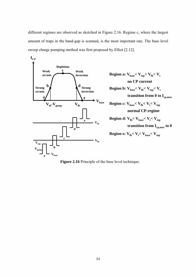
34
different regimes are observed as sketched in Figure 2.16. Regime c, where the largest
amount of traps in the band-gap is scanned, is the most important one. The base level
sweep charge pumping method was first proposed by Elliot [2.12].
Vth-Vgamp VfbVbase
ICP
Region a: Vbase< Vtop< Vfb< Vt
no CP current
Region b: Vbase< Vfb< Vtop< Vt
transition from 0 to Icp,max
Region c: Vbase< Vfb< Vt< Vtop
normal CP-regime
Region d: Vfb< Vbase< Vt< Vtop
transition from Icp,max to 0
Region e: Vfb< Vt< Vbase< Vtop
Strong accum.
a
b
c
d
e
Week accum.
Depletion Week inversion
Strong inversion
Vfb
Vth
Vbase
Vtop
Vgamp
e
d
c
b
a Figure 2.16 Principle of the base level technique.

35
A Accumulation e- from source and drain
B Inversione- in traps to substrate
Figure 2.17 Band diagrams applied periodic gate pulses.
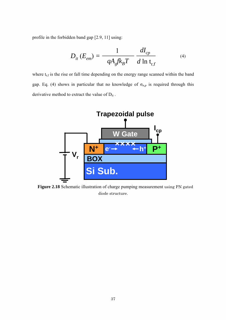
In this study, charge pumping method was used to measure the dependence of Dit on
size and shape of 3D structures, which are fabricated on a SOI wafer, with gated PIN
diodes [2.13-14]. As the fin structures were fabricated on an SOI wafer, the substrate
current cannot be measured. Therefore, PIN gated-diode was made as shown in Figure
2.18. This PIN gated-diode allows direct measurement of CP current thanks to the p+
region which acts as a ‘substrate’ contact.
Charge pumping current (Icp) measurements were performed by changing the rise (tr)
and fall time (tf) parameters of the trapezoidal pulse waves applied to the gate
electrode, so that the energy distribution of Dit in the energy band gap (Eg) can be
extracted [2.11]. This pulse fills the interface traps with electrons and holes, thereby
causing a recombination current to flow in the P+ and N+ regions of the gated diode. By

36
varying the base level Vbase from accumulation to inversion, the measured charge
pumping current ICP has a typical “hat” shape. The maximum of the two-level CP
current can be expressed as:
Icp = qfAg∫ Dit(E)dE = qfAgDitΔEem
Eem,e
Eem,h
where Ag is the gate area, f the frequency of the pulse signal, q the electron charge, and
Dit(E) the density of interface traps. The integration boundaries are the hole and the
electron emission levels Eem,h and Eem,e, which depends on temperature (T), the rise or
fall time (tr, tf), and the capture cross-section of electrons or holes (σn,p). Those energy
levels are given by
Eem,h = Ei + kBT ln vthniσp( |Vfb - Vt|Vgamp
tr )Eem,e = Ei- kBT ln vthniσp( |Vfb - Vt|
Vgamptf )
where Ei is the intrinsic Fermi level, Vfb the flat-band voltage, Vt the threshold voltage,
kB the Boltzmann constant, Vth the thermal velocity of carriers, ni the intrinsic carrier
density. Equation (1) shows a linear relation between Icp and frequency f.
The mean value Dit integrated over the band gap (between Eem,h and Eem,e) can be
measured by sweeping the frequency of the pulsed signal using:
Dit =qAgΔEem
1df
dIcp
The emission levels can be modulated by varying either tr, tf, or T. In particular,
varying tr while keeping tf constant, or reversely, allows to extract the Dit energy
(1)
(2)
(3)
37
profile in the forbidden band gap [2.9, 11] using:
Dit (Eem) =qAgfkBT
1d ln tr,f
dIcp
where tr,f is the rise or fall time depending on the energy range scanned within the band
gap. Eq. (4) shows in particular that no knowledge of σn,p is required through this
derivative method to extract the value of Dit .
Si Sub.
n
IcpW Gate
BOXN+ P+
Trapezoidal pulse
e- h+Vr
Figure 2.18 Schematic illustration of charge pumping measurement using PN gated
diode structure.
(4)
38
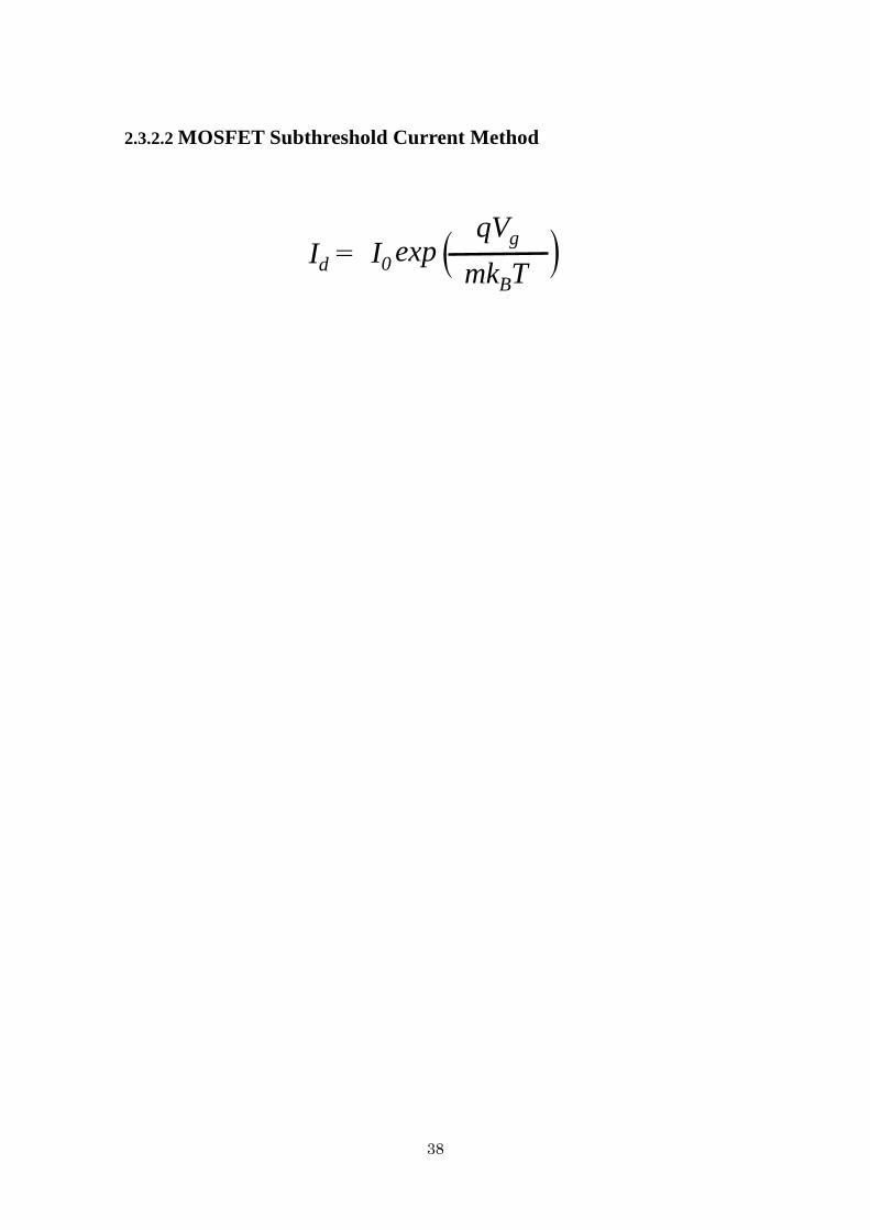
2.3.2.2 MOSFET Subthreshold Current Method
Id = I0 (expqVg
mkBT
(

39
References [2.1] K. Nishioka Hannosei, ion etching wo mochiita Si to SiO2 no etching
http://www-eng.kek.jp/meeting09/proceedings/pdf/h21gp404.pdf.
[2.2] H. Arai, Master Thesis, Tokyo Institute of Technology, Tokyo, 2010.
[2.3] N. Shigemori, Master Thesis, Tokyo Institute of Technology, Tokyo, 2011.
[2.4] A.J.Armini, S.N.Bunker, M.B.Spitzer, Non-mass-analyzed Ion Implantation
Equipment for high Volume Solar Cell Production, 16th IEEE Photovoltaic Specialists
Conference, (1982), pp. 895-899.
[2.5] G. Landis, A.J.Armini, A. C.Greenwald, R. A.Kiesling, Apparatus and
Technique for Pulsed Electron Beam Annealing for Solar Cell Production, 15th IEEE
Photovoltaic Specialists Conf., (1981), p.p. 976-980.
[2.6] Wolf.S, R.N.Tauber, Silicon Processing for the VLSI Era, Process Technology., 1,
(1986), pp. 532–533.
[2.7] R. C.Jaeger,. Film Deposition. Introduction to Microelectronic Fabrication.,
(2002)
[2.8] S.M. Sze, Semiconductor Devices: Physics and Technology
[2.9] G.V.Bosch, G.V.Groeseneken, IEEE Trans.Electron Devices, 38, (1991), pp.
1820-1831.
[2.10] J. S. Brugler and P. G. A. Jespers, Charge Pumping in MOS Devices, IEEE
Trans.Electron Devices, 16, (1969), pp. 297-302
[2.11] G. Groeseneken, H. Maes, N. Beltran, R. F. De Keersmaecker, A Reliable
Approach to Charge-Pumping Measurements in MOS Transistors, IEEE
Trans.Electron Devices, 31, (1984), pp. 42-53.
[2.12] A. B. M. Elliot, The Use of Charge Pumping Currents to Measure Surface State
40
Densities in MOS Transistors, Solid-State Electron., 19, (1976), p.p. 241-247.
[2.13] T. Elewa, H. Haddara, S. Cristoloveanu, M. Bruel, CHARGE PUMPING IN
SILICON ON INSULATOR STRUCTURES USING GATED P-I-N DIODES, J. Phys.
Colloq., 49, (1988), p.p. 137-140.
[2.14] K.Tachi, M. Casse, D. Jang, C. Dupré, A. Hubert, N. Vulliet, V. Maffini-Alvaro,
C. Vizioz, C. Carabasse, V. Delaye, J. M. Hartmann, G. Ghibaudo, H. Iwai, S.
Cristoloveanu, O. Faynot , T. Ernst, Relationship between mobility and high-k
interface properties in advanced Si and SiGe nanowires, Tech. Dig. of IEDM, (2009),
p.p. 313-316.
41
Chapter3 Interface-state density of 3D structure 3.1 Result and Discussion in planar SOI structure
3.1.1 Charge pumping current
3.1.2 Energy distribution of Dit
3.2 Result and Discussion in 3D structures
3.2.1 Charge pumping current
3.2.2 F.G. Annealing temperature dependence of Dit
3.2.3 Dit dependence on Wfin
3.3 Summary of this section
References
42
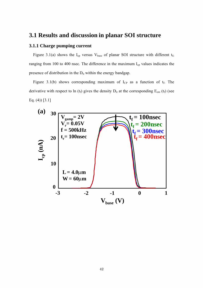
3.1 Results and discussion in planar SOI structure
3.1.1 Charge pumping current
Figure 3.1(a) shows the Icp versus Vbase of planar SOI structure with different tf,
ranging from 100 to 400 nsec. The difference in the maximum Icp values indicates the
presence of distribution in the Dit within the energy bandgap.
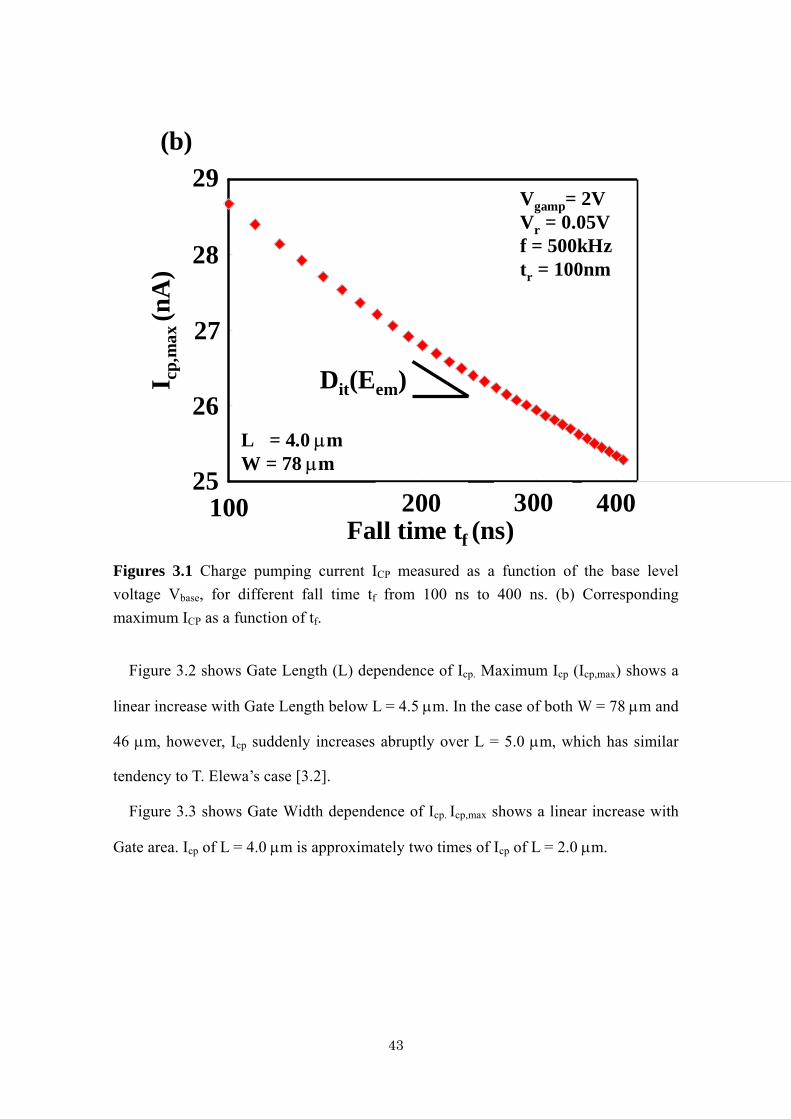
Figure 3.1(b) shows corresponding maximum of ICP as a function of tf. The
derivative with respect to ln (tf) gives the density Dit at the corresponding Eem (tf) (see
Eq. (4)) [3.1]
Vgamp= 2VVr= 0.05Vf = 500kHztr= 100nsec
Vbase (V)
I cp
(nA
)
0
10
20
30
-3 -2 -1 1
tf = 100nsectf = 200nsectf = 300nsectf = 400nsec
L = 4.0µmW = 60µm
(a)
0
43
Fall time tf (ns)400300200
26
27
28
29I c
p,m
ax(n
A)
100
Dit(Eem)
(b)
25
Vgamp= 2V Vr = 0.05V f = 500kHz tr = 100nm
L = 4.0 µmW = 78 µm
Figures 3.1 Charge pumping current ICP measured as a function of the base level voltage Vbase, for different fall time tf from 100 ns to 400 ns. (b) Corresponding maximum ICP as a function of tf.
Figure 3.2 shows Gate Length (L) dependence of Icp. Maximum Icp (Icp,max) shows a
linear increase with Gate Length below L = 4.5 µm. In the case of both W = 78 µm and
46 µm, however, Icp suddenly increases abruptly over L = 5.0 µm, which has similar
tendency to T. Elewa’s case [3.2].
Figure 3.3 shows Gate Width dependence of Icp. Icp,max shows a linear increase with
Gate area. Icp of L = 4.0 µm is approximately two times of Icp of L = 2.0 µm.

44
0 2 4 60
Length (µm)8 10 12
200
250I c
p,m
ax(n
A)
W = 78 µm
W = 46 µm
Vgamp= 2V Vr = 0.05V f = 500kHz tr = tf = 100ns
100
150
50
Figures 3.2 Gate Length dependence of Icp
0 1 3Width (µm)
L = 4.0 µm
L = 2.0 µm
Vgamp= 2V Vr = 0.05V f = 500kHz tr = tf = 100ns
0
25
30
I cp,
max
(nA
)
15
20
10
5
2 4 5 76 98
Figures 3.3 Gate Width dependence of Icp

45
Figures 3.4 shows frequency dependence of recombined charge per pulse period
(Qss). Incidentally, Icp is given by equation (5) [3.3].
= f Qss= f Ag q2 DitΔψs= f Ag q Nss
Icp
where ∆ψ is total sweep of the interface potential. Nss is interface state density (cm-2).
Therefore, Qss is expressed as equation (6).
Qss = Icp
f
On the Qss vs f curve, the pulse frequency f0 (frequency when the charge become zero)
is the X-intercept of the regression line. Frequency f0 is used to calculate the capture
cross sections as shown in equation (7) [3.4].
= σnσpσ
1vthni
= |Vfb - Vt|Vgamp
α(α-1)f0
And the slope of the regression line is used to calculate the mean interface-state
density Dit as shown in equation (8)
d Qssd log fSlope = log e
2qkBT Dit Ag=
Extracted σ values of 8.7 x 10⁻¹⁷ and 9.1 x 10⁻¹⁷ cm2 for W = 46 and 78 µm,
respectively, using f0 as shown Figure 3.4. Moreover, Extracted Dit values of 1.46 x
1010 and 1.91 x 1010 cm-2eV-1 for W = 46 and 78 µm, respectively, using eq.(8).
(5)
(6)
(7)
(8)

46
1 101 102 1030
1
2Q
ss(C
)
Frequency (kHz)
46 x 4.0 µm
78 x 4.0 µm
Vgamp= 2V Vr= 0.05V
(X 10-14)
f0
Figures 3.4 Frequency dependence of Qss.
47
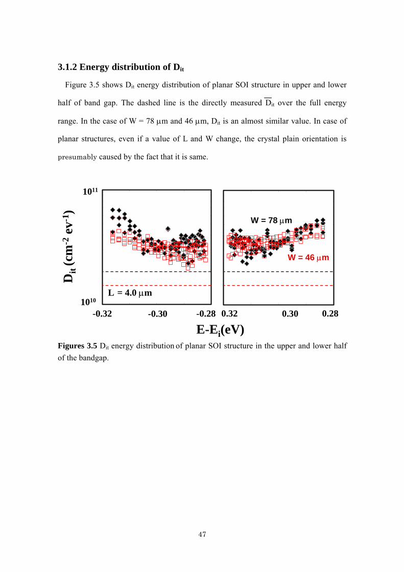
3.1.2 Energy distribution of Dit
Figure 3.5 shows Dit energy distribution of planar SOI structure in upper and lower
half of band gap. The dashed line is the directly measured Dit over the full energy
range. In the case of W = 78 µm and 46 µm, Dit is an almost similar value. In case of
planar structures, even if a value of L and W change, the crystal plain orientation is
presumably caused by the fact that it is same.
1.00E+10
1.00E+11
0.28 0.29 0.30 0.31 0.32
1.00E+10
1.00E+11
-0.32 -0.31 -0.30 -0.29 -0.28
1010
1011
Dit
(cm
-2ev
-1)
-0.32 -0.30 -0.28 0.32 0.30 0.28
E-Ei(eV)
L = 4.0 µm
W = 78 µm
W = 46 µm
Figures 3.5 Dit energy distribution of planar SOI structure in the upper and lower half of the bandgap.
48
3.2 Charge pumping current in 3D structures
3.2.2 F.G. Annealing temperature dependence of Dit
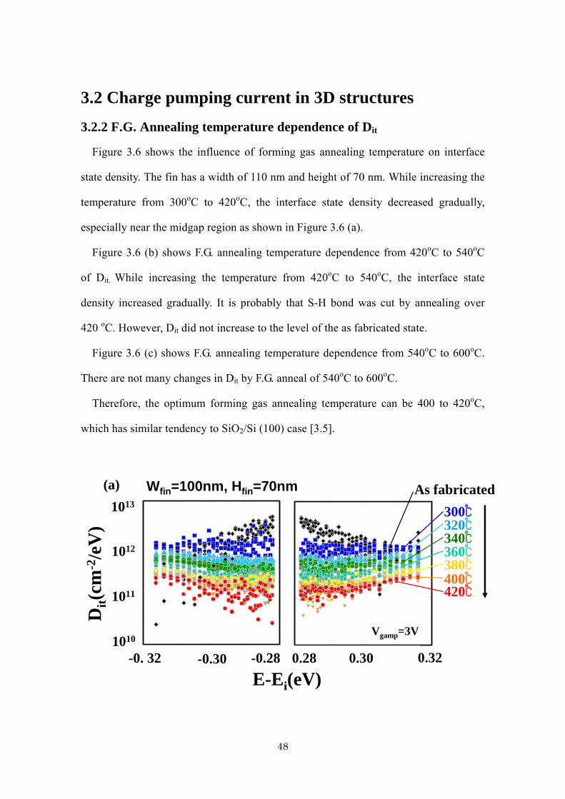
Figure 3.6 shows the influence of forming gas annealing temperature on interface
state density. The fin has a width of 110 nm and height of 70 nm. While increasing the
temperature from 300oC to 420oC, the interface state density decreased gradually,
especially near the midgap region as shown in Figure 3.6 (a).
Figure 3.6 (b) shows F.G. annealing temperature dependence from 420oC to 540oC
of Dit. While increasing the temperature from 420oC to 540oC, the interface state
density increased gradually. It is probably that S-H bond was cut by annealing over
420 oC. However, Dit did not increase to the level of the as fabricated state.
Figure 3.6 (c) shows F.G. annealing temperature dependence from 540oC to 600oC.
There are not many changes in Dit by F.G. anneal of 540oC to 600oC.
Therefore, the optimum forming gas annealing temperature can be 400 to 420oC,
which has similar tendency to SiO2/Si (100) case [3.5].
1.00E+10
1.00E+11
1.00E+12
1.00E+13
0.28 0.29 0.30 0.31 0.32
1.00E+10
1.00E+11
1.00E+12
1.00E+13
-0.32 -0.31 -0.30 -0.29 -0.28
E-Ei(eV)
1012
1011
1010
0.320.28 0.30-0.28-0.30-0. 32
As fabricated
420
300320340360380400
1013
Vgamp=3V
Dit(
cm-2
/eV
)
Wfin=100nm, Hfin=70nm(a)

49
E-Ei(eV)
1012
1011
1010
0.320.28 0.30-0.28-0.30-0. 32
1013
Vgamp=3V
Dit(
cm-2
/eV
)Wfin=100nm, Hfin=70nm
420440
480460
500520540
(b)
1.00E+11
1.00E+12
1.00E+13
0.28 0.29 0.30 0.31 0.32
1.00E+11
1.00E+12
1.00E+13
-0.32 -0.31 -0.30 -0.29 -0.28
E-Ei(eV)
1013
1012
1011
0.320.28 0.30-0.28-0.30-0. 32
Vgamp=3V
Dit(
cm-2
/eV
)
Wfin=100nm, Hfin=70nm
540560580600
(c)

50
1.00E+11
1.00E+12
1.00E+13
280 300 320 340 360 380 400 420 440 460 480 500 520 540 560 580 600
1011
1013
Dit
(cm
-2eV
-1)
1012
As fabricated
500400300 600F.G. anneal temparture(oC)
(d)E-Ei=0.29 eV
Figure 3.6 F.G. Annealing temperature dependence of Dit (a) from 300oC to 420oC (b) from 420oC to 540oC (c) from 420oC to 540oC (d)
Figure 3.7 shows the influence of F.G. annealing at 420 oC and F.G annealing at
420oC after F.G annealing at 600oC on Dit. Increased Dit value of the sample which
was annealed at 600oC was again recovered by annealing at 420oC.

51
1.00E+10
1.00E+11
1.00E+12
0.28 0.29 0.30 0.31 0.32
1.00E+10
1.00E+11
1.00E+12
-0.32 -0.31 -0.30 -0.29 -0.28
E-Ei(eV)
1012
1011
1010
0.320.28 0.30-0.28-0.30-0. 32
Vgamp=3V
Dit(
cm-2
/eV
)Wfin=100nm, Hfin=70nm
600oC→420oC
420
Figure 3.7 Influence of the recovery annealing on Dit

52
3.2.2 Dit dependence on Wfin
Figure 3.8 shows the energy distribution of interface state density distribution on
different fin width ranging from 90 to 105 nm. The figure on the left hand side shows
the lower half side of the bandgap and the one on the right hand side shows the upper
half of the bandgap. An increase in the interface state, especially near the midgap
region, has been observed with narrower fin structures. Compared to the interface state
distribution of Si (100) planar, fin structures have higher interface state density in all
the energy range.
1.00E+10
1.00E+11
1.00E+12
0.28 0.29 0.30 0.31 0.32
1.00E+10
1.00E+11
1.00E+12
-0.32 -0.31 -0.3 -0.29 -0.28
E-Ei(eV)
1012
1011
1010
Dit(
cm-2
/eV
)
0.320.28 0.30-0.28-0.30-0. 32
Vgamp=3V
F.G. anneal temparture:420oC
Wfin=105nm
Wfin=95nmWfin=100nm
Wfin=90nm
Hfin=70nm
Planar SOI
Figure 3.8 Dit dependence on Wfin
53
3.2 Summary of this section In this study, interface-state density of planar SOI and three dimensional Si
structures is measured by the charge pumping method using gated PIN diodes formed
on an SOI wafer.
In the case of planar SOI structures, even if a value of gate length or/and width
change, interface-state density is an almost similar value to what?.
In the case of three dimensional Si structures, while increasing the forming gas
annealing temperature from 300oC to 420oC, the interface-state density decreased
gradually, especially near the midgap region. On the other hand, while increasing the
forming gas annealing temperature from 420 oC to 540 oC, the interface-state density
increased gradually. Therefore, the optimum F.G. annealing temperature is considered
to be 400 to 420 oC, which are nearly the same as Si (100) planar case.
Moreover, the increase in interface-state density with decreasing the width of fin
structures was found. This result is further discussed in Chapter 4.
54
Reference
[3.1] M. Cassé, X. Garros, O. Weber, F. Andrieu, G. Reimbold, F. Boulanger, A study
of N-induced traps due to a nitrided gate in high-k/metal gate nMOSFETs and their
impact on electron mobility, Solid-State Electronics, 65-66, (2010), p.p. 139 - 145
[3.2] T. Elewa, H. Haddara, S. Cristoloveanu, M. Bruel, CHARGE PUMPING IN
SILICON ON INSULATOR STRUCTURES USING GATED P-I-N DIODES, J. Phys.
Colloq., 49, (1988), p.p. 137 - 140.
[3.3] E. Nicollian, J Brews, MOS physics and technology., Wiley & Sons, (1982)
[3.4] G. Groeseneken, H. Maes, N. Beltran, R. F. De Keersmaecker, A Reliable
Approach to Charge-Pumping Measurements in MOS Transistors, IEEE
Trans.Electron Devices, 31, (1984), p.p. 42 - 53.
[3.5] P. L. Castro, B. E. Deal, Low-Temperature Reduction of Fast Surface States
Associated with Thermally Oxidized Silicon, J. Electrochem. Soc, (1971), p.p. 280 -
286
55
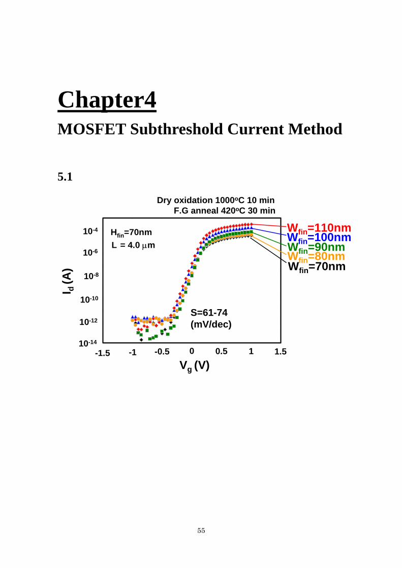
Chapter4 MOSFET Subthreshold Current Method 5.1
1.00E-14
1.00E-13
1.00E-12
1.00E-11
1.00E-10
1.00E-09
1.00E-08
1.00E-07
1.00E-06
1.00E-05
1.00E-04
1.00E-03
-1.5 -1 -0.5 0 0.5 1 1.5
-1 0 10.5Vg (V)
1.5-1.5
I d (A
)
F.G anneal 420oC 30 min
S=61-74 (mV/dec)
-0.5
Wfin=110nmHfin=70nm
10-10
10-12
10-14
10-4
10-6
10-8
Dry oxidation 1000oC 10 min
L = 4.0 µmWfin=100nmWfin=90nmWfin=80nmWfin=70nm
56
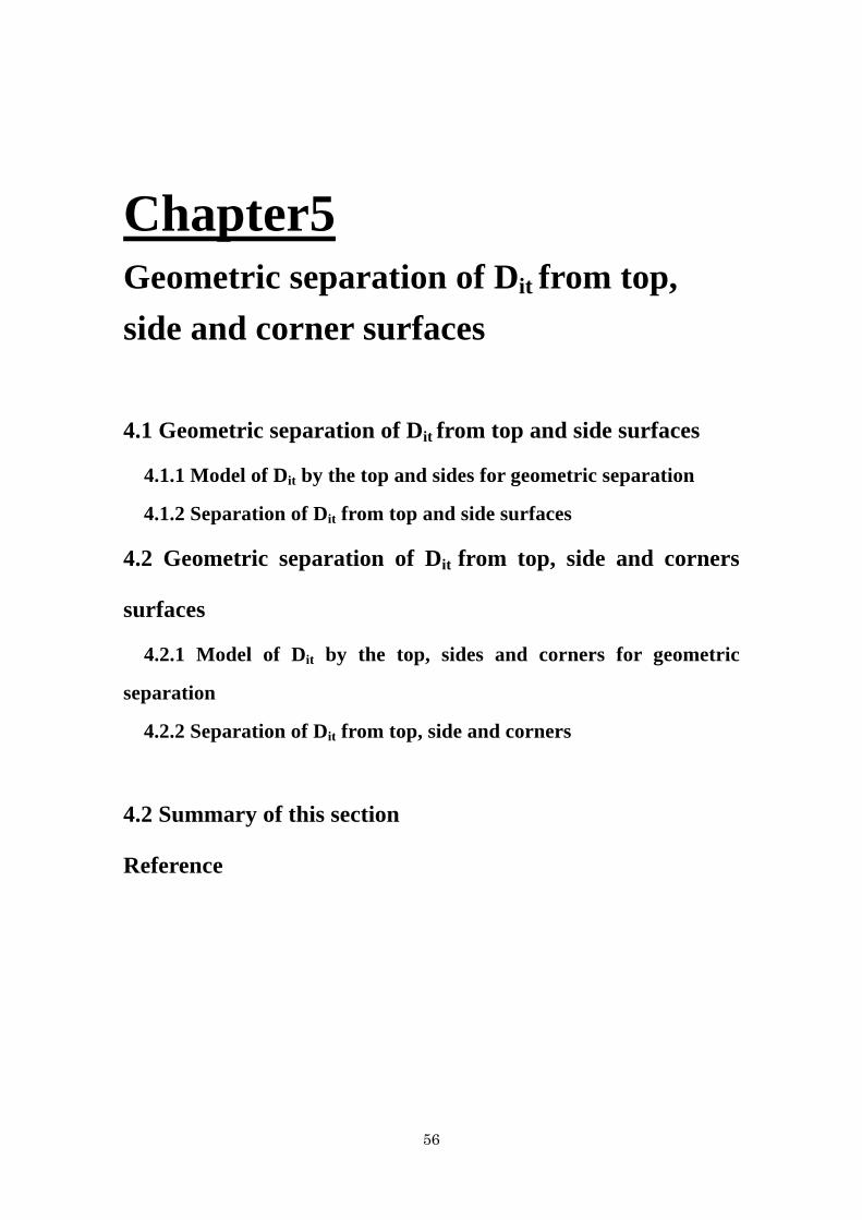
Chapter5 Geometric separation of Dit from top, side and corner surfaces 4.1 Geometric separation of Dit from top and side surfaces
4.1.1 Model of Dit by the top and sides for geometric separation
4.1.2 Separation of Dit from top and side surfaces
4.2 Geometric separation of Dit from top, side and corners
surfaces
4.2.1 Model of Dit by the top, sides and corners for geometric
separation
4.2.2 Separation of Dit from top, side and corners
4.2 Summary of this section
Reference

57
4.1 Geometric separation of Dit from top and side
surfaces
4.1.1 Model of Dit by the top and sides for geometric separation
Next, the interface states separation of top (Dit,top) and side surfaces (Dit,side) was
tio of the surfaces (That is, the channel areas were calculated as Wfin + Hfin × 2.) [4.1-3].
As a result, total Dit can be expressed as:
known
Dit =Wfin x Dit,top + 2Hfin x Dit,side
Wfin+ 2Hfin
where Wfin and Hfin were known value. Moreover, it is note that Dit,side include Dit of
corners.
BOXSub.
Top surface (100)Dit,top
Side surface (110)Dit,side
Figure 4.1 Assuming of Dit at top and the side surface

58
4.1.2 Separation of Dit from top and side surfaces Figure 4.2 shows the best fit of the interface state. One can see the increase in Dit
with narrower Wfin, presumably due to the increase in the proportion of the (110)
oriented sidewall area. Here, the value at the y axis is the interface state density of the
side surface. Assuming constant values of Dit for the top surface and sidewall as shown
in figure 4.3, the mean Dit values can be estimated. Note that the component of
sidewall includes the Dit located at the corner of the fin structure.
Extracted values of 1.29 × 10¹⁰ and 2.61 × 1011 cm-2 ev-1 for surface and sidewall,
respectively, showed the best match with the experimentally obtained data. Therefore,
one can expect a large Dit by extrapolation when the sidewall channel becomes
dominant.
Dit(
eV-1
cm-2
)
1.00E+11
1.00E+12
0 50 100 1501011
0 50 150 200Wfin(nm)
Hfin=70nm
1012
Dit of side surface
E-Ei=0.29 eV
Figure 4.2 Minimum Dit values on Wfin. Assuming two Dit values for top and side surfaces, the Dit trend can be well explained.

59
BOXSub.
Top surface (100)Dit~ 1.3 x 1011 cm-2/eV
Side surface (110)Dit ~ 2.6 x 1012 cm-2/eV
Figure 4.3 Extracted Dit of the top and side surface (with corner)
4.2.1 Model of Dit by the top, sides and corners for geometric
separation
Dit =(Wfin – 2∆) x Dit,top + 2Hfin x Dit,side + 2∆ x Dit,corner
Wfin+ 2Hfin known
Planar SOI Dit = 3.2 x1010cm-2/eV
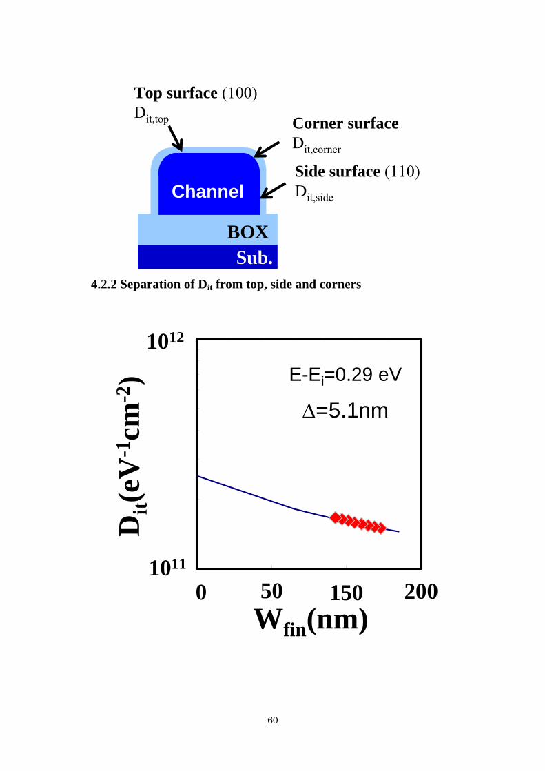
60
BOX
Channel
Sub.
Top surface (100)Dit,top
Side surface (110)Dit,side
Corner surfaceDit,corner
4.2.2 Separation of Dit from top, side and corners
1.00E+11
1.00E+12
0 50 100 1501011
0 50 150 200Wfin(nm)
1012
Dit(
eV-1
cm-2
) E-Ei=0.29 eV
∆=5.1nm
61
BOX
Channel
Sub.
Top surface (100)Dit,top~ 3.2 x 1010cm-2/eV
Side surface (110)Dit,side ~ 2.3 x 1011cm-2/eV
Corner surfaceDit,corner ~ 3.0 x 1011cm-2/eV
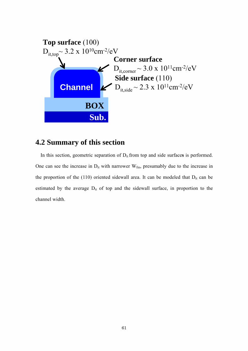
4.2 Summary of this section In this section, geometric separation of Dit from top and side surfaces is performed.
One can see the increase in Dit with narrower Wfin, presumably due to the increase in
the proportion of the (110) oriented sidewall area. It can be modeled that Dit can be
estimated by the average Dit of top and the sidewall surface, in proportion to the
channel width.
62
Reference
[4.1] M. Saitoh, Y. Nakabayashi, H. Itokawa, M. Murano, I. Mizushima, K. Uchida, T.
Numata, Short-Channel Performance and Mobility Analysis of <110>- and
<100>-Oriented Tri-Gate Nanowire MOSFETs with Raised Source/Drain Extensions,
VLSI Tech. Dig. (2010), pp.169 - 170.
[4.2] G. Groeseneken, F. Crupi, A. Shickova, S. Thijs, D. Linten, B. Kaczer, N. Collaert,
M. Jurczak, RELIABILITY ISSUES IN MUGFET NANODEVICES, Proceedings of
Int. Reliab. Phys. Symp., (2008), p.p. 52 - 60.
[4.3] G. Kapila, B. Kaczer, A. Nackaerts, N. Collaert, G. V. Groeseneken, Direct
Measurement of Top and Sidewall Interface Trap Density in SOI FinFETs, IEEE
Electron Dev. Lett., 28, (2007), p.p. 232 - 234

63

64
Chapter5 Conclusion of This Study 5.1 Conclusion
Recently, multi-gate or nanowire FET has been focused as it gives excellent short
channel effect immunity by better gate control of the channel potential. Thus, MOS
devices with three dimensional channels have been considered as one of the promising
candidates to overcome the scaling issues in planar FETs.
Generally, three dimensional channels consist of several or more crystallographic
orientation formed by plasma etching or oxidation process. Therefore, one of the
concerns with these structures is the presence of interfacial state density, which is
strongly dependent on the surface orientations.
In this study, the dependence of interface-state density on three dimensional Si body
with rectangular cross section was measured by charge pumping method with gated
PIN diodes formed on an SOI wafer.
The optimum F.G. annealing temperature is considered as 400 to 420 oC, which are
nearly same as Si (100) planar case. Fin structure has higher Dit value than SOI planar
case in any energy. The increase in Dit with decreasing the width of fin structures was
found. From Fin width dependency, Dit of 1.3 x 1010 cm-2/eV for top surface and 2.6 x
1011 cm-2/eV were extracted.
It can be modeled that Dit can be estimated by the average Dit of top and the sidewall
surface, in proportion to the channel width.

65
Acknowledgments
I would like to express my deepest gratitude to my supervisor at Tokyo Institute of
Technology, Professor Sugii Nobuyuki and Professor Hiroshi Iwai who provided
carefully considered feedback and valuable comments. They gave me a lot of chances
to attend international and domestic conferences. These opportunities become great
experiences for me.
I would like to thank Associate Professor Kuniyuki Kakushima for helpful
suggestions and discussions including design of mask pattern, fabrication processes,
and many encouragements for our study in Iwai laboratory.
I would like to thank Professor Takeo Hattori, Professor Kenji Natori, Professor
Kazuo Tsutsui, Professor Akira Nishiyama, Professor Yoshinori Kataoka and
Associate Professor Parhat Ahmet for useful advices and great help whenever I met
difficult and subtle problem.
I would like to thank research colleagues of Professor Iwai’s Laboratory members
for the kind friendship and active discussions. I’m so happy to get in Iwai laboratory
and meet the members. Especially, Daisuke Kitayama, Masahiro Koyama, Ryuji Hosoi,
Tasuku Kaneda and Takuya Suzuki, are the members who get in this laboratory in the
same year and have good friendships. I would like to thank their great support and
kindness.
I also express sincere gratitude to secretaries of Iwai laboratory, Ms. Akiko
Matsumoto and Ms. Masako Nishizawa.
Finally, I would like to thank my parents, my brother and my sisters for their great
and endless support and encouragement in all my life.

66
This study was partially supported by Nanoelectronics Project by New Energy and
Industrial Technology Development Organization (NEDO), Japan.
February, 2011
Kazuhiro Nakajima