materials, device designs, and integration approaches …
TRANSCRIPT
MATERIALS, DEVICE DESIGNS, AND INTEGRATION APPROACHES FOR TRANSIENT,
BIO-RESORBABLE SILICON ELECTRONIC SYSTEMS
BY
SUK WON HWANG
DISSERTATION
Submitted in partial fulfillment of the requirements
for the degree of Doctor of Philosophy in Materials Science and Engineering
in the Graduate College of the
University of Illinois at Urbana-Champaign, 2013
Urbana, Illinois
Doctoral Committee:
Professor John A. Rogers, Chair
Professor Paul V. Braun
Associate Professor Jianjun Cheng
Associate Professor Xiuling Li

ii
ABSTRACT
A remarkable feature of a silicon-based electronics is its capability to operate functionally
and physically invariant for many practical purposes. Here, we introduce a technology that offers
the opposite behavior: it gradually vanishes over time, in a well-controlled, programmed manner.
Devices that are ‘transient’ in this sense have potential applications that cannot be addressed with
conventional electronic devices, such as implantable biomedical devices that remain for
medically useful time periods, but then completely dissolve/resorb into the body. We report a set
of materials, manufacturing schemes, device components and theoretical design tools for a
silicon-based complementary metal oxide semiconductor (CMOS) technology and power
scavenging system with oscillators as a building block of wireless communication, which has this
type of ‘transient’ behavior, together with various integrated sensors. A transient silicon device
capable of delivering thermal therapy in an implantable mode and its demonstration in animal
models illustrate a system-level example of this technology.
Another discovery for this type of transient electronics is materials and fabrication
procedures that the key device processing steps occur on silicon wafer substrates, in schemes
compatible with established methods used in conventional microelectronics. The approach relies
on an unusual type of silicon on insulator wafer, and yields devices that use ultrathin sheets of
monocrystalline silicon for the semiconductor, thin films of magnesium for the electrodes and
interconnects, silicon dioxide and magnesium oxide for the dielectrics and silk for the substrates.
A range of component examples, with detailed measurements of their electrical characteristics
and dissolution properties, illustrate the capabilities. In vivo toxicity tests demonstrate
biocompatibility in sub-dermal implants. The results have significance for broad classes of
water-soluble, ‘transient’ electronic devices.

iii
ACKNOWLEDGEMENT
I would like to thank my advisor, Prof. John A. Rogers, for allowing me the opportunity to
work in his group, and for encouragement and motivation during Ph. D program. I am grateful to
Prof. Paul V. Braun, Prof. Xiuling Li and Prof. Jianjun Cheng as committee members for
invaluable comments and guidance for the direction of my research. I am also thankful to our
collaborators, Prof. Fiorenzo G. Omenetto at Tufts University and Prof. Yonggang Huang at
Northwestern Universtiy for their efforts to achieve experimental accomplishments.
I am also grateful to friends as a graudate student here at University of Illinois, Rak-Hwan,
Dae-Hyeong, Kyou-Hyun, Yun-Soung, Stanley, Jun-Kyul, Elliott and Ryan for their helps and
kindness, and basket guys, Jiyong, Jongro and Yuan for enjoying hoops and stress relax together.
I would especially like to thank my parents, sister and brother-in-law for unconditional
support and love all the time, and thankful to God for giving me health, wisdom and beautiful life.

iv
To My Family, for the opportunity of education with their support and love
v
TABLE OF CONTENTS
CHAPTER 1 ................................................................................................................................................... 1
A PHYSICALLY TRANSIENT FORM OF SILICON ELECTRONICS ..................................................... 1
1.1 Introduction .............................................................................................................................................. 1
1.2 Experiments .............................................................................................................................................. 1
1.3 Results and discussion .............................................................................................................................. 4
1.4 Conclusion ................................................................................................................................................ 9
1.5 Methods .................................................................................................................................................... 9
1.6 Reference .................................................................................................................................................19
1.7 Figures .....................................................................................................................................................21
CHAPTER 2 ..................................................................................................................................................47
BIOCOMPATIBILITY AND BIODEGRADABILITY OF A SINGLE CRYSTALLINE SILICON
NANOMEMBRANES (SiNMs) ...................................................................................................................47
2.1 Introduction .............................................................................................................................................47
2.2 Experiments .............................................................................................................................................48
2.3 Results and discussion .............................................................................................................................49
2.4 Conclusion ...............................................................................................................................................53
2.5 References ...............................................................................................................................................54
2.6 Figures .....................................................................................................................................................55
CHAPTER 3 ..................................................................................................................................................67
MATERIALS FOR BIORESORBABLE RADIO FREQUENCY ELECTRONICS ...................................67
3.1 Introduction .............................................................................................................................................67
3.2 Experiments .............................................................................................................................................68
3.3 Results and discussion .............................................................................................................................69
3.4 Conclusion ...............................................................................................................................................74
3.5 References ...............................................................................................................................................74
3.6 Figures ....................................................................................................................................................76
CHAPTER 4 ..................................................................................................................................................89
MATERIALS AND PROCESSES FOR TRANSIENT AND BIORESORBABLE HIGH PERFORMANCE
ELECTRONICS ............................................................................................................................................89
4.1 Introduction .............................................................................................................................................89
4.2 Experiments .............................................................................................................................................91
4.3 Results and discussion .............................................................................................................................93
4.4 Conclusion ...............................................................................................................................................98
4.5 References ...............................................................................................................................................98
4.6 Figures ..................................................................................................................................................101
CHAPTER 5 ................................................................................................................................................114
TRANSIENT, BIOCOMPATIBLE ELECTRONICS BASED ON ZNO ...................................................114
5.1 Introduction ...........................................................................................................................................114

vi
5.2 Experiments ...........................................................................................................................................115
5.3 Results and discussion ...........................................................................................................................116
5.4 Conclusion .............................................................................................................................................119
5.5 References .............................................................................................................................................119
5.6 Figures ..................................................................................................................................................122
CHAPTER 6 ................................................................................................................................................126
DEVICE DESIGN AND MANUFACTURING APPROACH FOR TRANSIENT ELECTRONIC
SYSTEM INTEGRATED ONTO BIODEGRADABLE AND BIOCOMPATIBLE POLYMER
SUBSTRATE ..............................................................................................................................................126
6.1 Introduction ...........................................................................................................................................126
6.2 Experiments ...........................................................................................................................................127
6.3 Results and discussion ...........................................................................................................................127
6.4 Conclusion .............................................................................................................................................130
6.5 References .............................................................................................................................................130
6.6 Figures ...................................................................................................................................................132
CHAPTER 7 ................................................................................................................................................137
SUMMARY AND PERSPECTIVE ............................................................................................................137

1
CHAPTER 1
A PHYSICALLY TRANSIENT FORM OF SILICON ELECTRONICS
1.1 Introduction
An overarching goal in the development of nearly any new class of electronics is to achieve high
performance operation in physical forms that undergo negligible change with time. Active and passive
materials, device and circuit layouts, and packaging strategies are each formulated individually and then
configured collectively to accomplish this outcome. We present concepts and strategies for electronics
that involve similar attention to engineering designs, but with the goal of achieving systems that physically
disappear at prescribed times and with controlled rates. Applications that could exploit this transient
behavior include implantable medical diagnostic and therapeutic devices that resorb in the body to avoid
adverse long-term effects, fieldable environmental sensors that dissolve to eliminate the need for collection
and recovery, and portable consumer devices that decompose to minimize costs and health risks associated
with recycling and management of hazardous waste streams. For these three examples, the desired
timescales for transience range from days/weeks, to months, to years, respectively. The approaches
reported here can address these and other application concepts with circuit components whose operational
characteristics match those of non-transient counterparts formed in the usual way on silicon wafer
substrates. When combined with transient sensors, actuators, power supplies and wireless control systems,
this technology provides levels of function that significantly exceed those available with recently reported
forms of organic electronics in which certain constituent materials are water soluble [1-3], or simple non-
transient transistors formed on bio-resorbable substrates [4].
1.2 Experiments
Doped single crystalline silicon nanomembranes (thickness ~300 nm, p-type) were
fabricat1ed from silicon-on-insulator (SOI, SOITEC, France) wafers to serve as active materials
1 From [Science 337, 1640-1644 (2012)]. Reprinted with permission from AAAS

2
for the semiconductor devices. High temperature diffusion of phosphorous (~950 C) and boron
(~1,000 C) defined highly doped regions for source and drain electrodes in transistors and for n
and p type areas of diodes, photodetectors and solar cells. The lateral dimensions of the doped Si
NMs were defined by reactive ion etching (RIE) with sulfur hexafluoride (SF6) gas. To release
the silicon from the SOI, the buried oxide was removed by wet etching with hydrofluoric acid
(HF, 49% Electronic grade, ScienceLab, USA). Individual Si NMs formed by this process were
transfer printed to a spin cast film of silk on a silicon wafer (as a temporary ‘carrier’ substrate).
Gate and interlayer dielectrics (MgO, or SiO2), as well as electrodes and interconnects (Mg) were
deposited by electron-beam evaporation through high resolution stencil masks. For the latter,
MgO layers served as adhesion promoters, except for the Mg/Si contacts needed for the
transistors, where Mg was either deposited directly or, for improved yields and adhesion strength,
with an 5 nm layer of Ti.
The sensitivity of silk to solvents and processes typically used in photolithography
motivated the use of high resolution shadow masking techniques for patterning metals and
dielectrics. The required stencil masks were made from uniform polyimide (PI) films (12.5 µm,
Kapton, Dupont, USA), with openings etched in desired geometries. The fabrication process
began with attachment of such a film onto a glass slide coated with 10:1 poly(dimethylsiloxane)
(monomer:catalyst, by weight) (PDMS, Sylgard 184, Dow Corning, USA). A metal layer (Cr/Au,
10/150 nm) was deposited by electron beam evaporation, patterned using photolithography and
etched with wet etchant. The metal served as a hard mask during dry etching through the PI films
with oxygen (O2) gas. After etching, the metal mask was removed by wet etching, and the
patterned PI films were carefully peeled away to form high resolution stencil masks.
Instead of a single Si NM, arrays of narrow Si nanoribbons (NRs) can be used, as a way
to accelerate transience through a process of disintegration that can enhance diffusive mass
transport. The fabrication in this case began with doped arrays of Si NRs defined using

3
procedures described in previous sections. Here, however, the buried oxide was only partially
removed from beneath the Si NRs, although completely removed in the intervening regions. Next,
patterning a layer of photoresist (AZ 5214) formed structures (i.e. anchor bars; 10 µm × 50 µm,
1.5µm thick) that tethered the Si NRs to their lithographically defined locations during a second
etching step to complete the removal of the buried oxide. Next, the arrays of Si NRs were
transfer printed onto a separate silicon substrate coated with a layer of silk. Evaporation of MgO
(150 nm) on selected areas through a polyimide shadow mask defined gate dielectrics and
adhesion promoting layers. Finally, source, drain, and gate electrodes (Ti/Mg, 5/200 nm) were
defined by a similar procedure, to complete the devices.
A series of dissolution tests of Si NMs were performed to study the detailed kinetics of
the process. The test structures for this purpose consisted of arrays of NMs in 3 3 µm square
geometries, formed on SOI wafers by photolithography and RIE. We investigated thicknesses of
35 nm, 70 nm, and 100 nm. The samples were placed into 50 mL of 1.0 M phosphate buffered
saline (PBS, pH 7.4, Sigma-Aldrich, USA) at either room temperature or temperatures close to
those of the human body (37 °C). The samples were removed from the PBS solution every two
days to measure the height of the Si NMs by atomic force microscopy (AFM, Asylum Research
MFP-3D, USA). The PBS solution was replaced every other day.
In order to prepare substrates and encapsulants, B. mori silkworm cocoons were cut and
boiled in a 0.02 M Na2CO3 solution to extract the glue-like sericin proteins. The remaining silk
fibroin was rinsed in Milli-Q water and dissolved in a LiBr solution at 60 °C for 4 h and then
dialyzed with distilled water using dialysis cassettes for a couple of days to remove LiBr. After
centrifugation and filtration to remove insoluble remnants, the silk solution was diluted to 5 to 7
wt % with ion-free distilled water and cast onto silicon substrates or glass slide to form ∼20 μm
thick films and kept drying out in air to form silk films.
Transient system can be used for implantable biomedical devices, such as thermal
therapy using wireless power transmission. The demonstration device consists of Si NM resistors,

4
with Mg inductive coils and interconnection lines, formed on a silk substrate, with a separate silk
package. Transfer printing of doped Si NMs was followed by deposition and patterning of a first
metal layer (Ti/Mg, 5/250 nm), an interlayer dielectric (MgO, 400 nm) and a second metal layer
(Ti/Mg, 10/800 nm). The device was then packaged with silk, as described previously. The
coupling frequency for wireless power transmission was ~70 MHz.
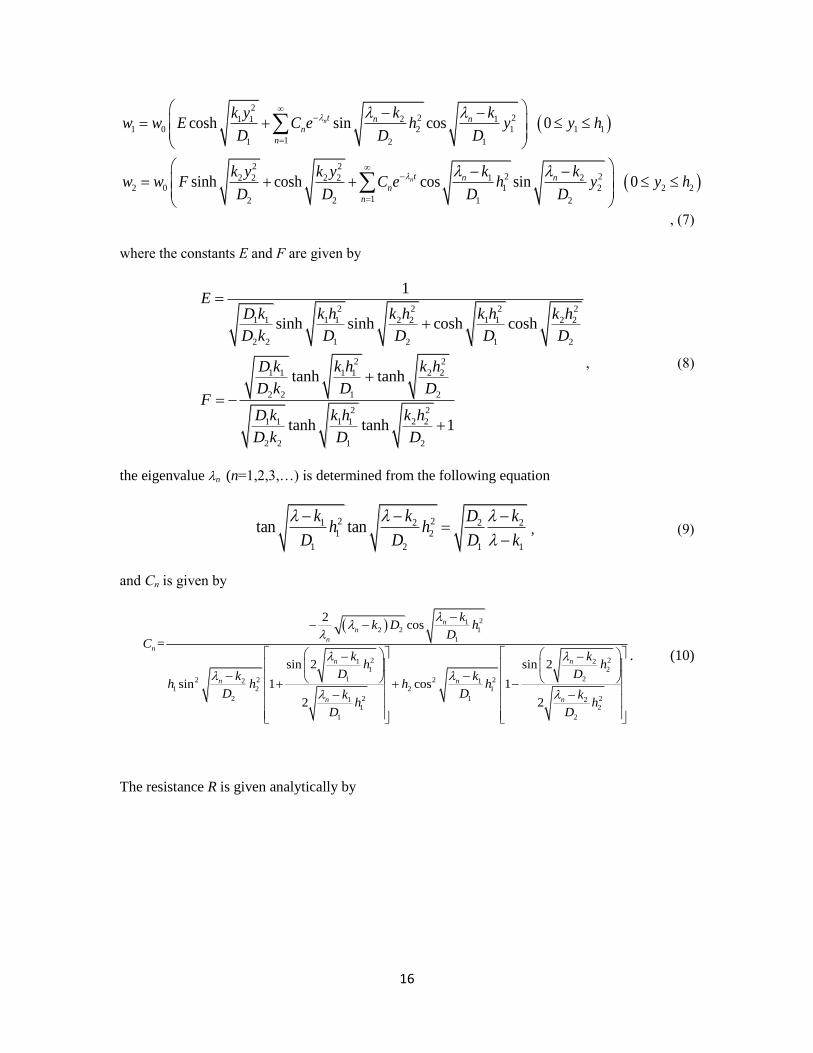
1.3 Results and discussion
Figure 1-1a, b and 2 provide images and schematic diagrams of a demonstration platform.
All of the components, ranging from the inductors, capacitors, resistors, diodes, transistors,
interconnects and crossovers, to the substrate and encapsulation layers, disintegrate and dissolve
when immersed in deionized (DI) water (Figure 1-1c). This example uses magnesium (Mg) for
the conductors, magnesium oxide (MgO) (silicon dioxide, SiO2, is also possible) for the
dielectrics, monocrystalline silicon (Si) nanomembranes (NMs) for the semiconductors, and silk
(which is water soluble and enzymatically degradable) [4, 5], for the substrate and packaging
material. The fabrication of systems such as this one involves a combination of transfer printing
(Si NMs) [6], physical vapor deposition through fine-line stencil masks (Mg, MgO, SiO2) and
solution casting (silk). More details on sample preparation can be found in [6]. As adhesion
promoters for Mg, we use MgO in certain cases and ultrathin layers of titanium in others. Device
yields without the titanium are 70~80 % with evaporated Mg, and >90 % with sputtered Mg.
The chemical reactions responsible for dissolution of each material appear in Figure 1-1d.
The Si NMs and layers of SiO2 are particularly important, due to their essential roles in high
performance transistors, diodes, photodetectors, solar cells, temperature sensors, strain gauges
and other semiconductor devices. The NM geometry is critical because it enables high
performance devices and planar architectures, minimizes the amount of material that must be
consumed during the transient step, and provides mechanics and processing options that are
favourable for heterogeneous integration onto substrates such as silk [4], as well as elastomers
5
that can provide modulus-matched interfaces to the body [7]. A typical transistor described here
requires less than ~1 µg of Si, which can be dissolved in as little as 30 L of bio-fluid [8].
Figure 1-3a presents atomic force micrographs of a Si NM (3 3 µm) with thickness of
70 nm, collected at different stages of dissolution in phosphate buffer solution (PBS; pH of 7.4) at
37 C, to simulate transience by bio-resorption (See Figure 1-4 and Figure 1-5a for additional
data.). The dissolution involves hydrolysis to form Si(OH)4 [9], according to: Si+4H2O <−>
Si(OH)4+2H2, where SiO2 can sometimes be involved as an intermediate [10]. The simplest
model of the kinetics, which depends strongly on pH, considers a constant reaction rate at the
water/Si NM interface [11]. The results capture experimental observations at both body
temperature (37 °C) (Figure 1-3c) and room temperature (25 °C) (Figure 1-5a) for a dissolution
rate of 4.5 nm/day and 2 nm/day, respectively, consistent with Arrhenius scaling [12].
Mechanisms involving diffusion into the materials can be important for Mg and MgO
deposited by electron beam evaporation and SiO2 formed by chemical vapour deposition, or as an
intermediate in the hydrolysis of silicon. In such cases, the kinetics can be described analytically
using models of reactive diffusion (Figure 1-3b) [6]. The results quantitatively account for relaed
behaviors in other materials for transient electronics, including those in Figure 1-1 [6]. Figure 1-
3d presents a meander trace of Mg (150 nm) on a thin film of MgO (10 nm; adhesion promoter),
in which the measured changes in resistance correlate well to those expected based on computed
changes in thickness (Figure 1-3e, Figure 1-6a and b) [6]. (Other examples appear in Figure 1-7)
This result connects a key electrical property to models of reactive diffusion, thereby suggesting
the capacity to use such analytics in conjunction with established circuit simulators as a
comprehensive design approach.
The timescales for NM-based electronic components can be extended, in controlled
amounts, by adding transient encapsulating layers and packaging materials; they can be reduced
by decreasing the critical dimensions or by physically structuring the materials in a way that
6
accelerates dissolution by disintegration (Figure 1-8). Figure 1-3e and 1-6 show results of
measured transience in a serpentine resistor of Mg, encapsulated with different thicknesses of
MgO, and with combinations of MgO and overcoats of silk. Corresponding modeling results are
also shown in [6]. Silk is attractive for this purpose because its solubility in water can be
programmed, over several orders of magnitude, through control of crystallinity [5, 13]. Other
biodegradable polymers can also be used, as shown in Figure 1-9.
Studies of transience at the device level are also important. Figure 1-3f shows examples
of metal oxide semiconductor field effect transistors (MOSFETs) formed using Si NMs, SiO2
gate dielectrics and Mg electrodes, with encapsulating layers of MgO and crystallized silk. The
devices show two-stage kinetics in their functional transience. Immersion in DI water for up to
~90 hours causes negligible change in key device characteristics. Functional degradation then
occurs in a relatively narrow time interval following this period of stable operation. The
encapsulation layers define the first timescale; the Mg electrodes define the second. The results
demonstrate that the transience time can be engineered in a way that is decoupled from system or
device level function.
These materials, fabrication techniques and modelling tools can yield components for
almost any type of transient electronic system, in CMOS designs. Figure 1-10 presents several
examples, including additional details on MOSFETs similar to those in Figure 1-3f, where both n-
and p-channel operation is possible. The resulting electrical properties for an n-channel device
include saturation and linear regime mobilities of 560 cm2/Vs and 660 cm
2/Vs, respectively,
on/off ratios of > 105, subthreshold slopes of 160 mV/dec (at Vd = 0.1 V) and width-normalized
current outputs of 0.34 mA/mm (at Vg = 5 V). These characteristics, as well as those of similar p-
channel devices, compare favorably to the performance of counterparts formed on silicon-on-
insulator (SOI) wafers [14]. (For the range of channel lengths investigated, contact resistances do
not limit performance. See Figure 1-11.) In all cases, the transience times of various elements in
an integrated system can be controlled by use of varied thicknesses and/or stack compositions, or

7
even via combination with non-transient materials. This last possibility is shown in a logic gate
(inverter) in the right hand frames of Figure 1-10c and d, where a non-transient metal (Au) serves
as source, drain and gate electrodes for two transistors joined by transient Mg interconnects.
Many other classes of semiconductor devices and passive components are possible with
examples in Figure 1-10, 1-12 and 1-13. The resistors and diodes can serve as temperature
sensors; the latter can also be used in photodetectors and solar cells, as shown in Figure 1-10 and
1-20. The Si NM diode and Mg resistive temperature sensors show sensitivities of -2.23 mV/°C
(change in voltage for a given current output) and 0.23%/°C (percentage change in resistance),
both of which are consistent with the behavior of conventional, non-transient devices [15].
Ultrathin silicon solar cells (~3 µm thick) provide fill factors of 66 % and overall power
conversion efficiencies of ~3 %, even without light trapping structures, backside reflectors or
anti-reflection coatings. Doped Si NMs can serve as strain gauges (Figure 1-10e, left), with
gauge factors of nearly ~40 (Figure 1-10f, left, and Figure 1-13b), comparable to those of state-
of-the art devices [16]. As an example of interconnected components, we built a transient digital
imaging system, consisting of collections of Si NM photodiodes with blocking diodes for passive
matrix addressing (Figure 1-10e, right), capable of capturing pictures when operated in a scanned
mode (Figure 1-10f, right, and Figure 13d). (See more details on device dimensions in Figure 1-
14.) The yield here is > 90%. (i.e. 58 out of 64 pixels were fully functional. See Figure 1-15.)
One possibility for power supply involves silicon solar cells such as those shown in Figure 1-13a.
Another uses inductors and capacitors like those in Figure 1-1a, 1-10a and 1-12 as wireless
antennas for near-field mutual inductance coupling to separately powered, external primary coils.
This option is interesting for implantable devices [4], made possible by the bio-compatibility of
the constituent materials (Figure 1-1), as established in unrelated contexts [6].
To demonstrate opportunities, we conducted a series of in vivo and in vitro experiments.
Various representative transient devices (e.g. Figure 1-1 and others) were fabricated, sealed in
silk packages, sterilized with ethylene oxide, and then implanted in the sub-dermal region of
8
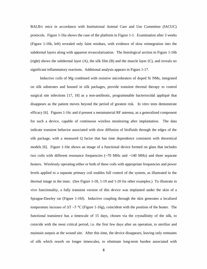
BALB/c mice in accordance with Institutional Animal Care and Use Committee (IACUC)
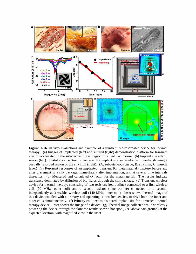
protocols. Figure 1-16a shows the case of the platform in Figure 1-1. Examination after 3 weeks
(Figure 1-16b, left) revealed only faint residues, with evidence of slow reintegration into the
subdermal layers along with apparent revascularization. The histological section in Figure 1-16b
(right) shows the subdermal layer (A), the silk film (B) and the muscle layer (C), and reveals no
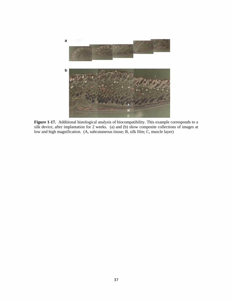
significant inflammatory reactions. Additional analysis appears in Figure 1-17.
Inductive coils of Mg combined with resistive microheaters of doped Si NMs, integrated
on silk substrates and housed in silk packages, provide transient thermal therapy to control
surgical site infections [17, 18] as a non-antibiotic, programmable bacteriocidal appliqué that
disappears as the patient moves beyond the period of greatest risk. In vitro tests demonstrate
efficacy [6]. Figures 1-16c and d present a metamaterial RF antenna, as a generalized component
for such a device, capable of continuous wireless monitoring after implantation. The data
indicate transient behavior associated with slow diffusion of biofluids through the edges of the
silk package, with a measured Q factor that has time dependence consistent with theoretical
models [6]. Figure 1-16e shows an image of a functional device formed on glass that includes
two coils with different resonance frequencies (~70 MHz and ~140 MHz) and three separate
heaters. Wirelessly operating either or both of these coils with appropriate frequencies and power
levels applied to a separate primary coil enables full control of the system, as illustrated in the
thermal image in the inset. (See Figure 1-18, 1-19 and 1-20 for other examples.) To illustrate in
vivo functionality, a fully transient version of this device was implanted under the skin of a
Sprague-Dawley rat (Figure 1-16f). Inductive coupling through the skin generates a localized
temperature increase of ΔT ~5 °C (Figure 1-16g), coincident with the position of the heater. The
functional transience has a timescale of 15 days, chosen via the crystallinity of the silk, to
coincide with the most critical period, i.e. the first few days after an operation, to sterilize and
maintain asepsis at the wound site. After this time, the device disappears, leaving only remnants
of silk which resorb on longer timescales, to eliminate long-term burden associated with

9
additional exogenous implant material.
1.4 Conclusion
Concepts reported here establish a baseline of materials, modeling approaches,
manufacturing schemes and device designs for transient electronic systems, sensors, actuators and
power supply. The Si NMs are critically important elements because their use enables
sophisticated semiconductor components with both active and passive functionality. For the
dielectrics and conductors, additional possibilities range from collagen to poly(lactic-co-glycolic
acid) and from iron to zinc, respectively. Alternative modes of transience include absorption,
corrosion, sublimation and de-polymerization. The rates for these processes could, conceivably,
be adjustable in real-time and/or sensitive to the properties of the surrounding environment,
determined by chemical or biological events, or changes in temperature, pressure, or light.
Combining such possibilities in transience with ideas in soft, ‘tissue-like’ electronics will further
expand opportunities for applications in biomedical devices [7].
1.5 Methods
Two ~100 μm silk fibroin films, cut into areas of ~5 cm × 5 cm, were cross-linked via
lamination at 120 °C for 60 s, to achieve maximum β-sheet crystallinity and complete adhesion of
the silk layers. The films were stacked, and then one edge was sealed by re-lamination with 10
μL of ~6 % silk fibroin solution as an adhesion layer. The silk substrate for the functional device
was left uncrosslinked, and placed in between the two cross-linked films. Finally, the other three
sides were sealed by the same method, fully encapsulating the sample in between the two films.
Excess film was trimmed from the edges to minimize the size of the encapsulated sample for
implantation.
For in vivo evaluation, female BALB/c mice (6 - 8 weeks old) and female albino
Sprague-Dawley rats were anesthetized with an intraperitoneal injection of a ketamine/xylazine
10
mix. The depth of anesthesia was monitored by palpebral and withdrawal reflexes to confirm that
the animal had reached “stage 3” of anesthesia. The back was shaved and cleaned at the incision
site with 70 % ethanol, followed by a betadine surgical scrub. Once stage 3 was confirmed, a
small longitudinal incision was made through the skin and the sterile implants (ethylene oxide
sterilized) were inserted. The incision was closed with a Dexon 5-0 suture. The animal was
monitored until ambulatory and given a dose of analgesia (Buprenorphine subcutaneously) as
soon as surgery was completed.
It is very critical to adjust the entire lifetime of transient device using very efficient
encapsulation methods, here several different encapsulation layers were used to control the
dissolution rate. Test structures used to study this process involved traces of Mg (300 nm),
patterned by a lift-off process followed by e-beam evaporation, on glass slides. Parts of the traces
were coated with various encapsulating materials: MgO (400nm or 800nm), silk, PLGA
(poly(lactic-co-glycolic acid) 85:15, Mw 50,000-70,000, Sigma-Aldrich, USA) or collagen film
(Devro, USA). For silk encapsulation, several cycles of coating and treatment were repeated:
dipping the samples into a silk solution, drying at 65 °C, treating with methanol to increase beta
sheet content and then drying. Multiple coating and subsequent methanol treatments were to
increase the total thickness of the silk films. PLGA was coated by placing a PDMS enclosure
around the area to be coated and then filling the internal volume with a PLGA solution. The
solution was allowed to evaporate, leaving only PLGA as an encapsulating layer. Collagen films
were attached to glass edges using a concentrated solution of PLGA, which was then allowed to
dry, leaving a solid but flexible, adhesive layer between the collagen and glass. The results are
shown in Figure 1-9.
In addition to the dissolution rate of transient materials, we studied the behavior at the
device level and demonstrated strategies to control the transience. In particular, we first
constructed several different transient devices, including n-channel MOSFETs, silicon diodes,
logic gates (NAND) and Mg resistors. The fabrication, except for the Mg resistors, started with

11
high temperature doping processes for the Si NMs (300 nm thick), as described in previous
sections. Transfer printed Si NMs of this type served as the semiconductor layers. Layers of SiO2
(100 nm thick) deposited by PECVD served as the gate dielectrics for the individual MOSFETs
and those that were used in the NAND gates. Similar layers, but with 400 nm thickness, provided
interlayer dielectrics. The electrodes consisted of Mg (300 or 400 nm thick) deposited by
electron beam evaporation. The device layouts appear in Figure 1-21.
Encapsulation layers of MgO (400 nm thick) and crystallized silk (approximately 70 µm
thick) provided transient barriers to DI water. In all cases, system configurations allowed
continuous probing of electrical properties through remotely located electrode pads that
connected to the devices, submerged in DI water at room temperature contained in a removable
well made of PDMS, as in Figure 1-22. The results, summarized in Figure 1-23, show kinetics
with two distinct timescales: the first, and longest, corresponds to transience in the encapsulation
layers; the second is due to the dissolution of active layers in the devices, where disappearance of
Mg occurs first. These behaviors illustrate transience at the device level. The outcomes also
demonstrate the ability to define transience times with materials (i.e. encapsulation layers) that do
not play active roles in device operation. In this manner, transience time can be engineered in a
manner that is independent of electrical function.
To study transience in vivo, we built a metamaterial antenna with overall dimensions
~1.35 cm × 1.35 cm (made of 400 nm Mg and coated with 600 nm MgO as the protection layer),
to achieve a designed resonant frequency of ~1.8 GHz, on an untreated/water-dissolvable silk
film (~50 μm thick) encapsulated in silk package (~2 × 2 cm and ~100 μm thick) sealed along the
edges via hot embossing using a few silk drops as an adhesive, as described previously. Upon
implantation under the skin of a female albino Sprague-Dawley rat, this construction prevents
direct contact between the device and the surrounding tissues. Transience in this case is defined
mainly by diffusion of bio-fluids through edges of the silk pocket. The antenna was examined by
measuring the resonant responses with a network analyzer (HP 8753D) before and after the
12
encapsulation process and prior to implantation. In vivo responses were recorded on day 0 (right
after the implantation), day 4, day 8 and day 15 (when the resonance of antenna was barely
detectable), as shown in Figure 1-16c. The device was retrieved thereafter, showing resorption
into the tissue matrix with signs of faint and disconnected Mg traces.
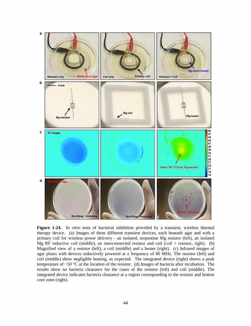
Devices with designs similar to those described previously were placed beneath a ~3 mm
thick agar plate loaded with Escherichia coli bacteria (ATCC 25922, American Type Culture
Collection, Manassas VA). The bacteria was reconstituted and expanded according to the
provided instructions, and the liquid cultures were grown for 18-24 hours to an optical density
(OD600) of 0.8 (corresponding to a viable count of ~107 CFU/mL). Three different device
structures were separately examined. The first two were controls, and consisted of Mg resistors
and Mg RF inductive coils, both in isolation. The third was the fully functional device (i.e. Mg
resistor connected to a Mg RF inductive coil). In all three cases, wireless power was applied at
80 MHz by an external RF supply with a separately located primary coil (1 turn, diameter = 5 cm,
12 AWG), at an input of ~33 dBm (i.e. 2 watts). The temperature profile of the bacterial-loaded
agar plate was monitored in real time using a thermal camera (FLIR SC645, FLIR Inc.). The
images showed negligible heating in the cases of the control samples, and heating to ~50 °C in
the center of the plate (corresponding to the heater position) for the functional device. After ~30
minutes of heating, the agar plates were placed in a 37 °C incubator overnight to allow lawn
growth. Visual inspection showed local absence of bacteria in the region heated by the device,
and no noticeable change for the controls. The results are shown in Figure 1-24.
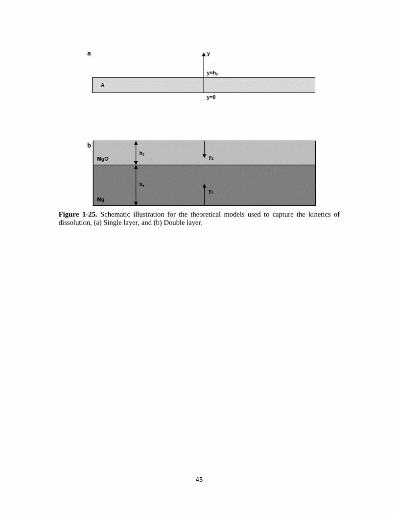
The dissolution kinetics can be described using analytical models of reactive diffusion
(Figure 1-3b) in which the rate limiting step is defined by diffusion of water and hydroxide ions
into the material and simultaneous reaction throughout the thickness direction y, according to
2
2
w wD kw
y t
[19-21], where D and k are the diffusivity for water and the reaction constant
between the porous material (A) and PBS, respectively, and w is the concentration of water. In

13
this model, for times, t, before complete physical disappearance, the thickness of the porous
material (h) decreases in an approximately linear fashion with t, according to
2
0 0tanhh h kDt kh D , (1)
where h0 is initial thickness, 2 0 A AA H OM M w n , M(H2O) and M(A) are the
molar masses of water and porous material A, respectively, w0 is the initial water concentration,
nA is the number of water molecules reacting with A, and A is the mass density of A. The
critical time for the thickness to reach zero is approximately given by
1
2
0 0tanhct kh D h kD
. For a line of Mg, for example, the resistance is given by
R0×(h/h0)-1
, and R0 is the initial resistance. This relationship provides the basis for comparison
results to experiment, which appear in Figure 1-3.
a. Single layer (magnesium or silicon oxide) dissolution
The boundary conditions (Figure 1-25a) for the reactive diffusion Equation (1) are
constant water concentration 0
0y hw w
at water/porous material (A) interface and zero water
flux 0
0y
w y
at the bottom surface of A. The initial condition is zero water concentration
000 0
tw y h
. The solution was obtained by the method of separation of variables as
22
20
20
2
1
2
0 2221 0200
11cosh
12, 2 cos
21cosh
2
nkhDt
nDh
n
kyn
yDw y t w e nhkhkh
nDD
.
(2)
Its product with the reaction constant k gives the mass of water in A (per unit volume), which in
turn gives the mass of dissolute A (per unit volume) to be A 2A H OkwM n M since nA

14
water molecules react with one A atom. Its integration over both the thickness direction y and
time t gives the net A during dissolution as
2220
20
2
0 0
2
0 0
2 10
220 0
22 2 221A 2 0 0 20
, ,
tanhA 1
1 2H O 1
2
Si
khDtn
Dh
nSi
kh wh Dtf
h h D
khw M kh Dt eD
n M D h kh khn
D D
. (3)
For k and D in the present study, the summation on the left hand side of the above equation is
negligible, which leads to Eq. (1).
Equation (1) applies for Mg since two water molecules react with one Mg atom,
2220
20
2 10
220 0
22 2 2210 2 0 0 20
tanhMg 1
1 22 H O 1
2
khDtn
Dh
nMg
khw M khh Dt eD
h M D h kh khn
D D
, (4)
where 3
Mg =1.738 g cm is the mass density of Mg. For Mg initial thickness h0=300 nm and
initial resistance (per unit length) R0=1.06 Ω/mm, the resistance (per unit length) R=R0(h/h0)-1
in
Figure 1-3e agrees well with the experiments for the reaction constant k=1.2×10⁻³
s-1
and
diffusivity D=6.0×10⁻¹²
cm2/s. Here k for Mg is much larger than that for Si because the water-
Mg reaction is much faster (hours to dissolute Mg versus weeks to dissolute Si). The critical time
tc for the complete dissolution of Mg is 38.4 min, which agrees well with 40 min for open circuit
in experiments.
Similarly, the reaction constant and diffusivity for SiO2 are obtained from the
experiments for PECVD SiO2 shown in Figure 1-5 as k=1.5×10⁻⁶
s-1
, D=1.0×10⁻¹⁶
cm2/s at room
temperature (Figure 1-5b) and k=3.0×10⁻⁶
s-1
and D=2.0×10⁻¹⁶
cm2/s at body temperature (Figure
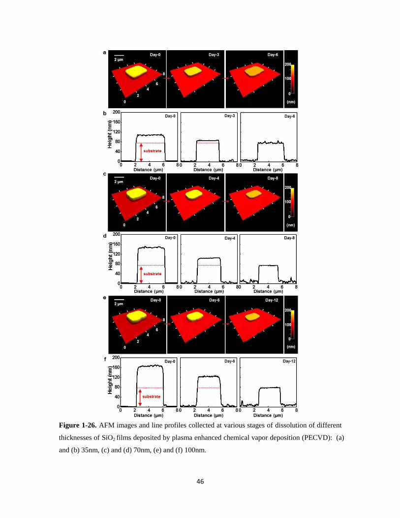
1-5c) [9, 10, 22]. The related AFM study is shown in Figure 1-26.
15
b. Double layer (MgO/Mg) dissolution
The local coordinate systems for the Mg and MgO layers, denoted by subscripts 1 and 2,
respectively, are shown in Figure 1-25b. For Mg, the reactive diffusion equation with zero water
flux condition at the bottom surface and initial condition are
1
2
1 11 1 1 1 12
1
1
1 0
1 1 10
0
0
0 0
y
t
w wD k w y h
y t
w
y
w y h
. (5)
For MgO, the governing equation with constant water concentration at water/MgO
interface and initial condition are
2
2
2 22 2 2 2 22
2
2 0 0
2 2 20
0
0 0
y
t
w wD k w y h
y t
w w
w y h
.
(6)
The continuity of the concentration and flux of water molecules across the MgO/Mg
interface requires 1 1 2 2
1 2y h y hw w
and
1 1 2 2
1 21 2
1 2y h y h
w wD D
y y
.
The solution of Eqs. (5) and (6) is obtained by the method of separation of variables as
16
22 22 11 1
1 0 2 1 1 1
11 2 1
2 22 21 22 2 2 2
2 0 1 2 2 2
12 2 1 2
cosh sin cos 0
sinh cosh cos sin 0
n
n
t n nn
n
t n nn
n
k kk yw w E C e h y y h
D D D
k kk y k yw w F C e h y y h
D D D D
, (7)
where the constants E and F are given by
2 2 2 2
1 1 1 1 2 2 1 1 2 2
2 2 1 2 1 2
2 2
1 1 1 1 2 2
2 2 1 2
2 2
1 1 1 1 2 2
2 2 1 2
1
sinh sinh cosh cosh
tanh tanh
tanh tanh 1
ED k k h k h k h k h
D k D D D D
D k k h k h
D k D DF
D k k h k h
D k D D
, (8)
the eigenvalue n (n=1,2,3,…) is determined from the following equation
2 21 2 2 2
1 2
1 2 1 1
tan tank k D k
h hD D D k
, (9)
and Cn is given by
212 2 1
1
2 21 21 2
1 22 2 2 22 11 2 2 1
2 22 11 21 2
1 2
2cos
=
sin 2 sin 2
sin 1 cos 1
2 2
nn
n
n
n n
n n
n n
kk D h
DC
k kh h
D Dk kh h h h
D Dk kh h
D D
. (10)
The resistance R is given analytically by
17
0
2211 1
1
21 0 1 1 222
1 22 211 11
11
sinh sinMg
1 1 sin2 H O
n
n
tn n
nMg n n
RR
kk hh
k w M D DC kEt e h
M Dkk hh
DD
.
(11)
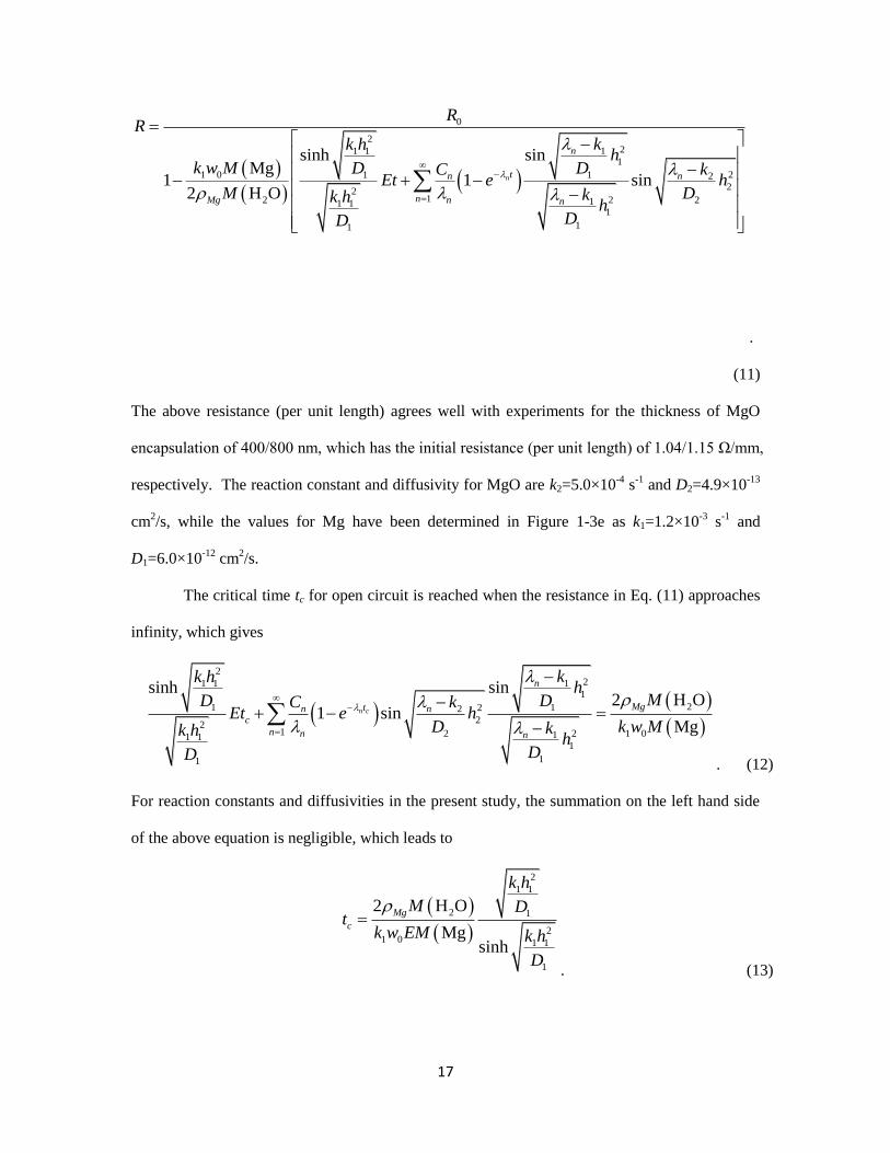
The above resistance (per unit length) agrees well with experiments for the thickness of MgO
encapsulation of 400/800 nm, which has the initial resistance (per unit length) of 1.04/1.15 Ω/mm,
respectively. The reaction constant and diffusivity for MgO are k2=5.0×10⁻⁴
s-1
and D2=4.9×10⁻¹³
cm2/s, while the values for Mg have been determined in Figure 1-3e as k1=1.2×10
-3 s
-1 and
D1=6.0×10⁻¹²
cm2/s.
The critical time tc for open circuit is reached when the resistance in Eq. (11) approaches
infinity, which gives
2211 1
1
21 1222
21 22 1 011 1
1
11
sinh sin2 H O
1 sinMg
n c
n
Mgtn nc
n n n
kk hh
MD DC kEt e h
D k w Mkk hh
DD
. (12)
For reaction constants and diffusivities in the present study, the summation on the left hand side
of the above equation is negligible, which leads to
2
1 1
2 1
21 0 1 1
1
2 H O
Mgsinh
Mg
c
k h
M Dt
k w EM k h
D
. (13)
18
It gives the critical time of 3.5 and 13 hours for the thickness of MgO encapsulation of 400 and
800 nm, respectively, which agrees reasonably well with experiments in Figure 1-3e.
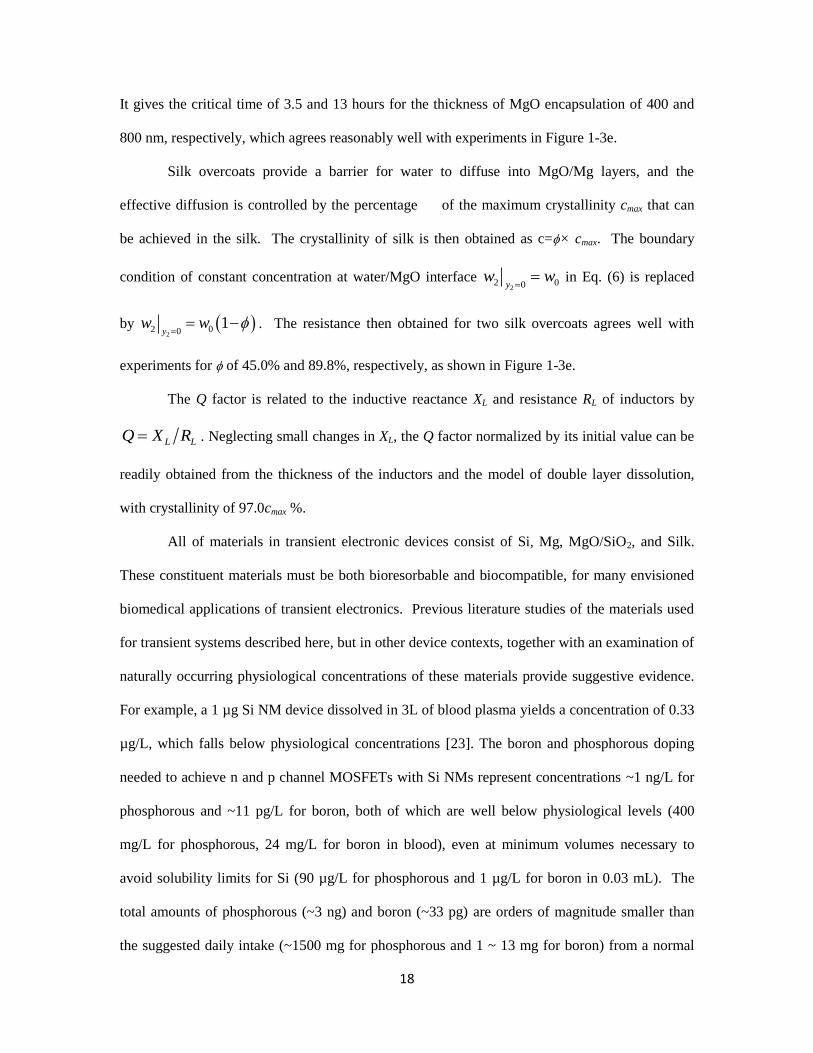
Silk overcoats provide a barrier for water to diffuse into MgO/Mg layers, and the
effective diffusion is controlled by the percentage of the maximum crystallinity cmax that can
be achieved in the silk. The crystallinity of silk is then obtained as c=× cmax. The boundary
condition of constant concentration at water/MgO interface 2
2 0 0yw w
in Eq. (6) is replaced
by 2
2 0 01
yw w
. The resistance then obtained for two silk overcoats agrees well with
experiments for of 45.0% and 89.8%, respectively, as shown in Figure 1-3e.
The Q factor is related to the inductive reactance XL and resistance RL of inductors by
L LQ X R . Neglecting small changes in XL, the Q factor normalized by its initial value can be
readily obtained from the thickness of the inductors and the model of double layer dissolution,
with crystallinity of 97.0cmax %.
All of materials in transient electronic devices consist of Si, Mg, MgO/SiO2, and Silk.
These constituent materials must be both bioresorbable and biocompatible, for many envisioned
biomedical applications of transient electronics. Previous literature studies of the materials used
for transient systems described here, but in other device contexts, together with an examination of
naturally occurring physiological concentrations of these materials provide suggestive evidence.
For example, a 1 µg Si NM device dissolved in 3L of blood plasma yields a concentration of 0.33
µg/L, which falls below physiological concentrations [23]. The boron and phosphorous doping
needed to achieve n and p channel MOSFETs with Si NMs represent concentrations ~1 ng/L for
phosphorous and ~11 pg/L for boron, both of which are well below physiological levels (400
mg/L for phosphorous, 24 mg/L for boron in blood), even at minimum volumes necessary to
avoid solubility limits for Si (90 µg/L for phosphorous and 1 µg/L for boron in 0.03 mL). The
total amounts of phosphorous (~3 ng) and boron (~33 pg) are orders of magnitude smaller than
the suggested daily intake (~1500 mg for phosphorous and 1 ~ 13 mg for boron) from a normal

19
diet [24-27]. Moreover, porous silicon and silica nanoparticles are well established as viable
candidates for bioresorbable drug delivery applications [28, 29]. Mg and Mg alloys have been
demonstrated in biodegradable stents. In particular, Mg is already used as structural material in
certain types of intravascular stents [30]. MgO has been used as coatings for these and related
structures [31], as well as for iron-based nanoparticle contrast agents for magnetic resonance
imaging [32]. Silk is approved for clinical use in resorbable surgical sutures and soft tissue
scaffolds [5]. The amounts of material utilized or envisioned for transient electronic constructs
are orders of magnitudes lower than those experimentally proven to have acceptable
biocompatibility and, in certain cases, established roles in clinical use.
1.6 Reference
[1] C. J. Bettinger, Z. Bao, Adv. Mater. 22, 651 (2010).
[2] M. Irimia-Vladu et al., Adv. Funct. Mater. 20, 4069 (2010).
[3] C. Legnani et al., Thin Solid Films 517, 1016 (2008).
[4] D.-H. Kim et al., Nat. Mater. 9, 511 (2010).
[5] Y. Wang et al., Biomaterials 29, 3415 (2008).
[6] Information on materials and methods is available on Science Online.
[7] D.-H. Kim et al., Science 333, 838 (2011).
[8] R. K. Iler, J. of Colloid Interface Sci. 43, 399 (1973).
[9] J. D. Rimstidt, H. L. Barnes, Geochim. Cosmochim. Ac. 44, 1683 (1980).
[10] M. Morita, T. Ohmi, E. Hasegawa, M. Kawakami, M. Ohwada, J. Appl. Phys. 68, 1272
(1990).
[11] H. Seidel, L. Csepregi, A. Heuberger, H. Baumgartel, J. Electrochem. Soc. 137, 3612 (1990).
[12] R. D. Levine, Molecular Reaction Dynamics (Cambridge University Press, Cambridge,
2005).
[13] X. Hu et al., Biomacromolecules 12, 1686 (2011).
20
[14] H.-J. Chung et al., Adv. Funct. Mater. 21, 3029 (2011).
[15] S. Santra, P. K. Guha, S. Z. Ali, I. Haneef, F. Udrea, IEEE Sens. J. 10, 997 (2010).
[16] S. M. Won et al., IEEE T. Electron Dev. 58, 4074 (2011).
[17] National Nosocomial Infections Surveillance (NNIS) report, data summary from October
1986-April 1996, issued May 1996. A report from the National Nosocomial Infections
Surveillance (NNIS) System, Am. J. Infect. Control 24, 380 (1996).
[18] D. J. Anderson et al., PLoS One 4, 1 (2009).
[19] P. V. Danckwerts, Tran. Faraday Soc. 46, 300 (1950).
[20] P. Hawtin, R. Murdoch, Chem. Eng. Sci. 19, 819 (1964).
[21] M. N. Ozisik, H. J. Nordwall, Nucl. Sci. Eng. 44, 310 (1971).
[22] M. Tomozawa, K. M. Davis, Mater. Sci. Eng. A 272, 114 (1999).
[23] W. Becker et al., The EFSA Journal 60, 1 (2004).
[24] M. R. Naghii, M. Mofid, A. R. Asgari, M. Hedayati, M.-S. Daneshpour, J. Trace. Elem. Med.
Bio. 25, 54 (2011).
[25] J. Capala et al., J. Neuro-Oncol. 62, 135 (2003).
[26] G. A. Block, T. E. Hulbert-Shearon, N. W. Levin, F. K. Port, Am. J. Kidney Dis. 31, 607
(1998).
[27] V. R. Young et al., Dietary Reference Intakes for Calcium, Phosphorus, Magnesium,
Vitamin D, and Fluoride (National Academy Press, Washington, DC, 1997).
[28] J.-H. Park et al., Nat. Mater. 8, 331 (2009).
[29] B. G. Trewyn, J. A. Nieweg, Y. Zhao, V. S. -Y. Lin, Chem. Eng. J. 137, 23 (2008).
[30] F. Witte, Acta Biomater. 6, 1680 (2010).
[31] S. Shen, P. S. Chow, F. Chen, R. B. H. Tan, Chem. Pharm. Bull. 55, 985 (2007).
[32] C. Martinez-Boubeta et al., Nanomedicine: NBM 6, 362 (2010).
21
1.7 Figures
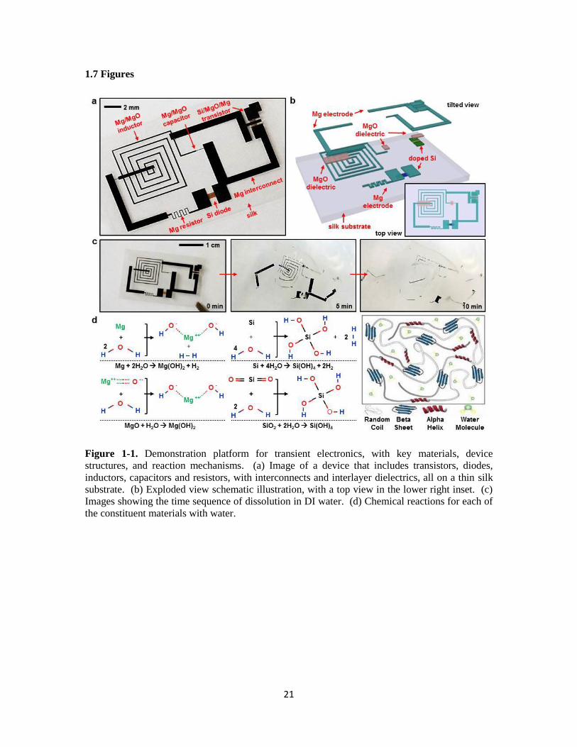
Figure 1-1. Demonstration platform for transient electronics, with key materials, device
structures, and reaction mechanisms. (a) Image of a device that includes transistors, diodes,
inductors, capacitors and resistors, with interconnects and interlayer dielectrics, all on a thin silk
substrate. (b) Exploded view schematic illustration, with a top view in the lower right inset. (c)
Images showing the time sequence of dissolution in DI water. (d) Chemical reactions for each of
the constituent materials with water.
22
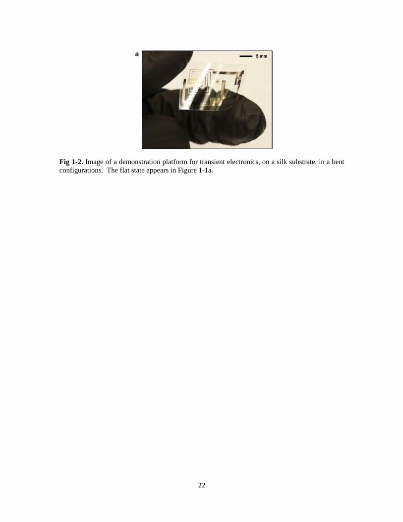
Fig 1-2. Image of a demonstration platform for transient electronics, on a silk substrate, in a bent
configurations. The flat state appears in Figure 1-1a.

23
Figure 1-3. Experimental studies of transient electronic materials, devices and corresponding
theoretical analysis. (a) Atomic force microscope (AFM) topographical images of a Si NM
(initial dimensions: 3 µm 3 µm 70 nm), at various stages of hydrolysis in phosphate buffered
saline (PBS). (b) Diagram of the processes of reactive diffusion used in models of transience. (c)
Experimental (symbols) and theoretical (lines) results for time dependent dissolution of Si NMs
(35 nm:black; 70 nm: blue; 100 nm: red) in PBS at 37 °C. (d) Optical microscope images of the
dissolution of a serpentine trace of Mg (150 nm thick) on top of a layer of MgO (10 nm thick) in
DI water at room temperature. (e) Experimental (symbols) and theoretical (lines) results of
dissolution kinetics of similar traces of Mg (300 nm thick) with different encapsulation layers:
MgO (400 nm, red; 800 nm, blue) and silk (condition i, cyan; condition ii, purple). (f)
Measurements of transience in operational characteristics of n-channel transistors encapsulated by
MgO and crystallized silk (picture in the inset on the left) and then immersed in DI water. The
results show the drain current (Id) at a drain voltage Vd = 0.1 V as a function of gate voltage (Vg)
at various times (left), and at Vg = 5 V as a function of time (right).
24
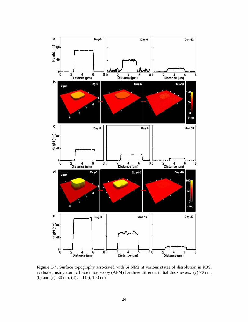
Figure 1-4. Surface topography associated with Si NMs at various states of dissolution in PBS,
evaluated using atomic force microscopy (AFM) for three different initial thicknesses. (a) 70 nm,
(b) and (c), 30 nm, (d) and (e), 100 nm.

25
Figure 1-5. Measured (symbols) and calculated (lines) time dependent change in the thicknesses
of thin layers of transient electronic materials in PBS. (a) Si NM at room temperature, in which
the calculations correspond to simple surface reaction, (b) PECVD SiO2 at room temperature, (c)
PECVD SiO2 at 37 °C.
26
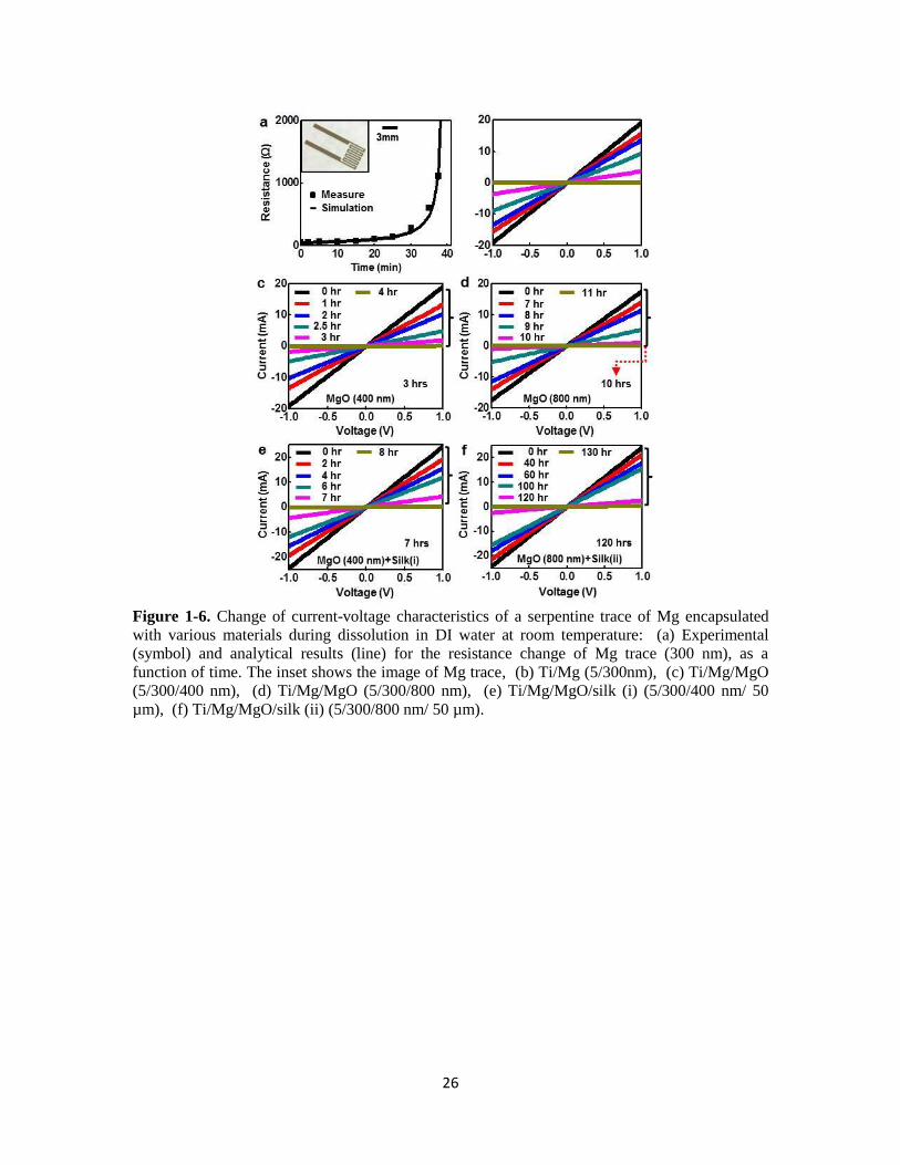
Figure 1-6. Change of current-voltage characteristics of a serpentine trace of Mg encapsulated
with various materials during dissolution in DI water at room temperature: (a) Experimental
(symbol) and analytical results (line) for the resistance change of Mg trace (300 nm), as a
function of time. The inset shows the image of Mg trace, (b) Ti/Mg (5/300nm), (c) Ti/Mg/MgO
(5/300/400 nm), (d) Ti/Mg/MgO (5/300/800 nm), (e) Ti/Mg/MgO/silk (i) (5/300/400 nm/ 50
µm), (f) Ti/Mg/MgO/silk (ii) (5/300/800 nm/ 50 µm).

27
Figure 1-7. Time dependent dissolution of transient electronic materials in DI water at room
temperature. (a) MgO (150 nm) and (b) Mg (300 nm), with a 5 nm layer of Ti as an adhesion
promoter.
28
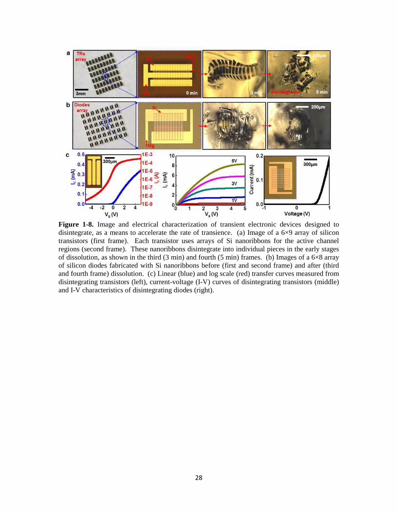
Figure 1-8. Image and electrical characterization of transient electronic devices designed to
disintegrate, as a means to accelerate the rate of transience. (a) Image of a 6×9 array of silicon
transistors (first frame). Each transistor uses arrays of Si nanoribbons for the active channel
regions (second frame). These nanoribbons disintegrate into individual pieces in the early stages
of dissolution, as shown in the third (3 min) and fourth (5 min) frames. (b) Images of a 6×8 array
of silicon diodes fabricated with Si nanoribbons before (first and second frame) and after (third
and fourth frame) dissolution. (c) Linear (blue) and log scale (red) transfer curves measured from
disintegrating transistors (left), current-voltage (I-V) curves of disintegrating transistors (middle)
and I-V characteristics of disintegrating diodes (right).
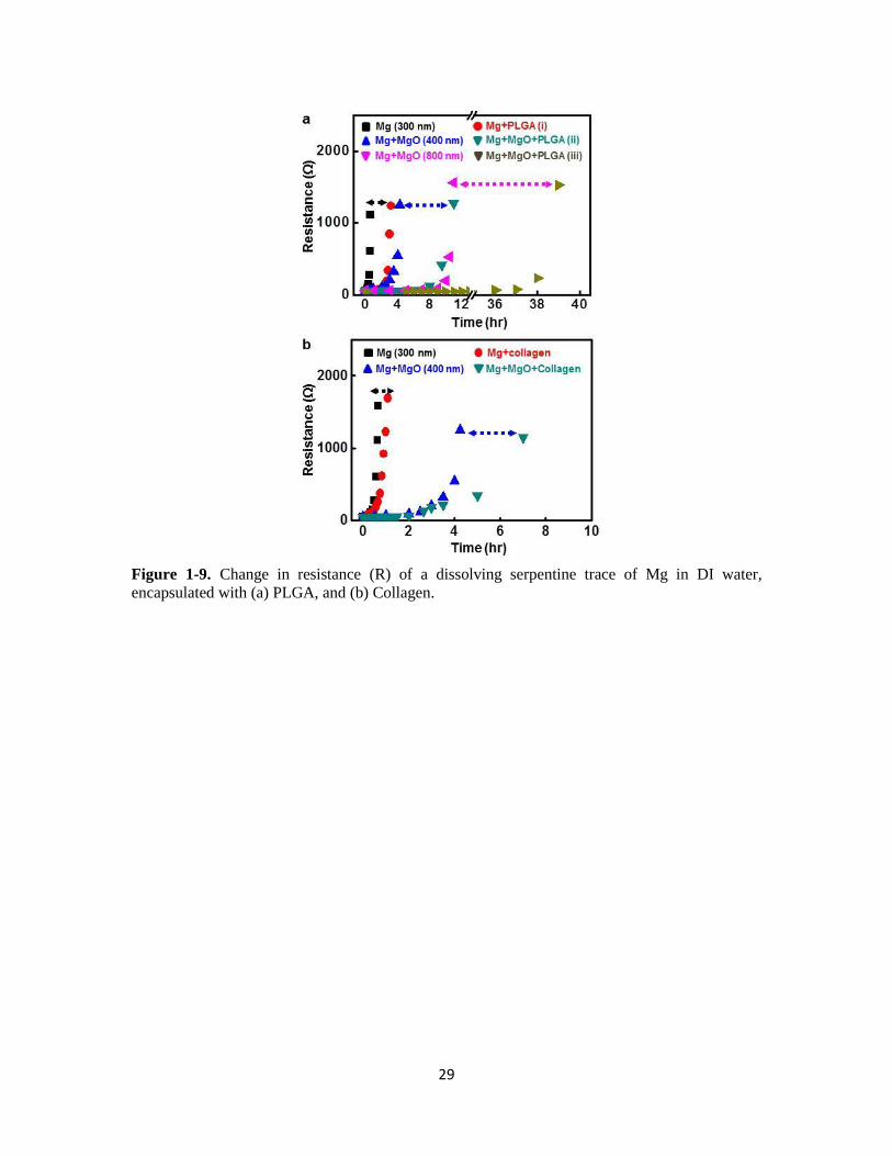
29
Figure 1-9. Change in resistance (R) of a dissolving serpentine trace of Mg in DI water,
encapsulated with (a) PLGA, and (b) Collagen.
30
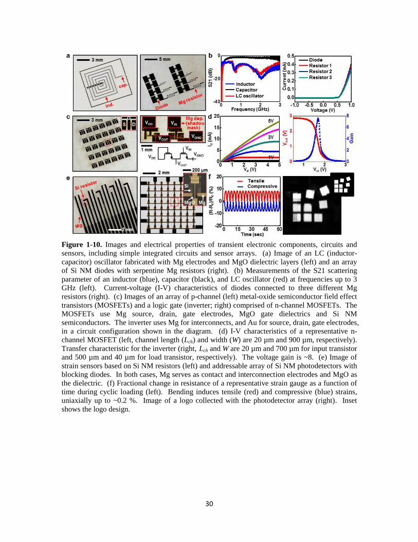
Figure 1-10. Images and electrical properties of transient electronic components, circuits and
sensors, including simple integrated circuits and sensor arrays. (a) Image of an LC (inductor-
capacitor) oscillator fabricated with Mg electrodes and MgO dielectric layers (left) and an array
of Si NM diodes with serpentine Mg resistors (right). (b) Measurements of the S21 scattering
parameter of an inductor (blue), capacitor (black), and LC oscillator (red) at frequencies up to 3
GHz (left). Current-voltage (I-V) characteristics of diodes connected to three different Mg
resistors (right). (c) Images of an array of p-channel (left) metal-oxide semiconductor field effect
transistors (MOSFETs) and a logic gate (inverter; right) comprised of n-channel MOSFETs. The
MOSFETs use Mg source, drain, gate electrodes, MgO gate dielectrics and Si NM
semiconductors. The inverter uses Mg for interconnects, and Au for source, drain, gate electrodes,
in a circuit configuration shown in the diagram. (d) I-V characteristics of a representative n-
channel MOSFET (left, channel length (Lch) and width (W) are 20 µm and 900 µm, respectively).
Transfer characteristic for the inverter (right, Lch and W are 20 µm and 700 µm for input transistor
and 500 µm and 40 µm for load transistor, respectively). The voltage gain is ~8. (e) Image of
strain sensors based on Si NM resistors (left) and addressable array of Si NM photodetectors with
blocking diodes. In both cases, Mg serves as contact and interconnection electrodes and MgO as
the dielectric. (f) Fractional change in resistance of a representative strain gauge as a function of
time during cyclic loading (left). Bending induces tensile (red) and compressive (blue) strains,
uniaxially up to ~0.2 %. Image of a logo collected with the photodetector array (right). Inset
shows the logo design.

31
Figure 1-11. (a) Comparison of electrical responses of n-channel MOSFETs that use Mg and Au
source/drain electrodes, evaluated by their width-normalized (W) resistance as a function of
channel length (Lch) at gate voltages of 4V, 5V, and 6V. (b) Measured, length (L) normalized
resistances (R) of Mg and Au traces for multiple line widths, each for two different thicknesses,
150 nm, and 300 nm, respectively. (c) Transfer curves (left), and I-V characteristics (right) from
n-channel MOSFETs that use Mg and Au source/drain electrodes.
32
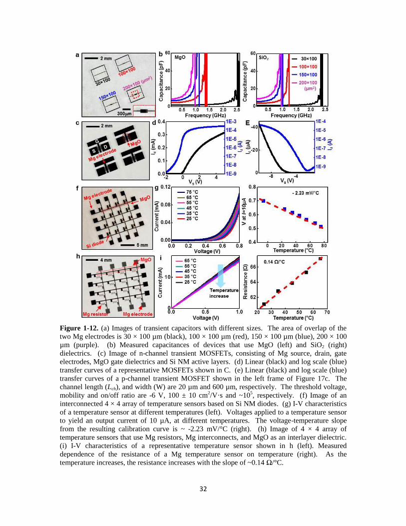
Figure 1-12. (a) Images of transient capacitors with different sizes. The area of overlap of the
two Mg electrodes is 30 × 100 µm (black), 100 × 100 µm (red), 150 × 100 µm (blue), 200 × 100
µm (purple). (b) Measured capacitances of devices that use MgO (left) and SiO2 (right)
dielectrics. (c) Image of n-channel transient MOSFETs, consisting of Mg source, drain, gate
electrodes, MgO gate dielectrics and Si NM active layers. (d) Linear (black) and log scale (blue)
transfer curves of a representative MOSFETs shown in C. (e) Linear (black) and log scale (blue)
transfer curves of a p-channel transient MOSFET shown in the left frame of Figure 17c. The
channel length (Lch), and width (W) are 20 µm and 600 µm, respectively. The threshold voltage,
mobility and on/off ratio are -6 V, 100 ± 10 cm2/V·s and ~10
5, respectively. (f) Image of an
interconnected 4 × 4 array of temperature sensors based on Si NM diodes. (g) I-V characteristics
of a temperature sensor at different temperatures (left). Voltages applied to a temperature sensor
to yield an output current of 10 µA, at different temperatures. The voltage-temperature slope
from the resulting calibration curve is ~ -2.23 mV/°C (right). (h) Image of 4 × 4 array of
temperature sensors that use Mg resistors, Mg interconnects, and MgO as an interlayer dielectric.
(i) I-V characteristics of a representative temperature sensor shown in h (left). Measured
dependence of the resistance of a Mg temperature sensor on temperature (right). As the
temperature increases, the resistance increases with the slope of ~0.14 Ω/°C.

33
Figure 1-13. (a) Image of solar cells that use ~3 µm thick bars of Si and Mg interconnects (left).
Current density and power measured from a representative device as a function of voltage (right)
when illuminated using light from a solar simulator. (b) Experimental (symbol) and analytical
(line) results of the fractional change in resistance of a silicon resistor as a function of applied
tensile (red), and compressive strain (blue). (c) I-V characteristics of a representative pixel
shown in the right frame of Figure 17e. The curves labeled dark (red) and bright (blue)
correspond to measurements preformed with a light source in the on and off states, respectively.
(d) Various images obtained using a passive matrix, 8 × 8 array of transient photodetectors,
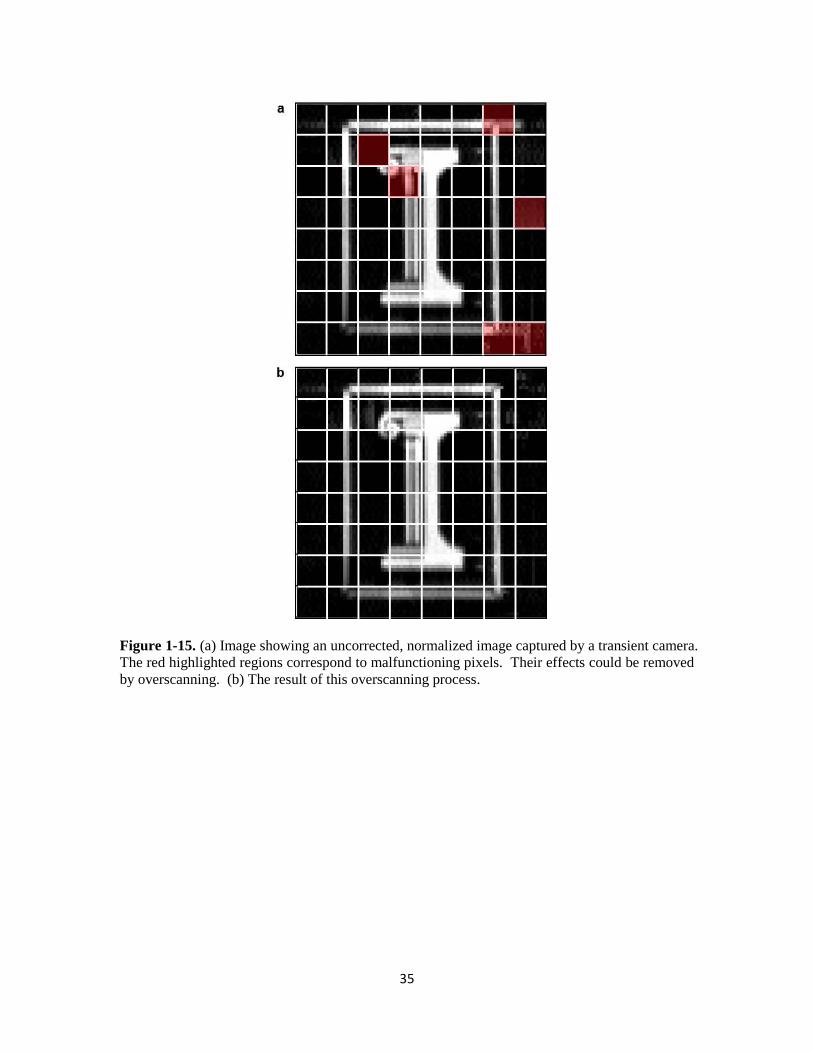
operated in a mode in which the object is scanned and a collection of recorded images is
combined to improve the effective resolution. Each inset shows the original object pattern. A
simple optics set-up containing an object, a diffusive light source, a plano-convex lens, and a
separate data acquisition program were used. The distance between the lens and source image
was 98 millimeters. In certain cases, an overscanning procedure was used to remove the effects of
malfunctioning pixels.
34
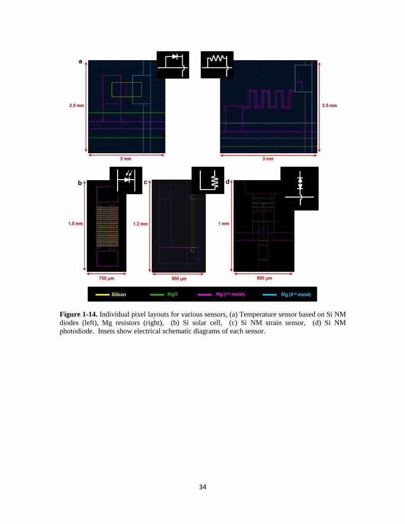
Figure 1-14. Individual pixel layouts for various sensors, (a) Temperature sensor based on Si NM
diodes (left), Mg resistors (right), (b) Si solar cell, (c) Si NM strain sensor, (d) Si NM
photodiode. Insets show electrical schematic diagrams of each sensor.
35
Figure 1-15. (a) Image showing an uncorrected, normalized image captured by a transient camera.
The red highlighted regions correspond to malfunctioning pixels. Their effects could be removed
by overscanning. (b) The result of this overscanning process.
36
Figure 1-16. In vivo evaluations and example of a transient bio-resorbable device for thermal
therapy. (a) Images of implanted (left) and sutured (right) demonstration platform for transient
electronics located in the sub-dermal dorsal region of a BALB-c mouse. (b) Implant site after 3
weeks (left). Histological section of tissue at the implant site, excised after 3 weeks showing a
partially resorbed region of the silk film (right). (A, subcutaneous tissue; B, silk film; C, muscle
layer) (c) Resonant responses of an implanted, transient RF metamaterial structure before and
after placement in a silk package, immediately after implantation, and at several time intervals
thereafter. (d) Measured and calculated Q factor for the metamaterial. The results indicate
transience dominated by diffusion of bio-fluids through the silk package. (e) Transient wireless
device for thermal therapy, consisting of two resistors (red outline) connected to a first wireless
coil (70 MHz; outer coil) and a second resistor (blue outline) connected to a second,
independently addressable, wireless coil (140 MHz; inner coil). Inset shows thermal image of
this device coupled with a primary coil operating at two frequencies, to drive both the inner and
outer coils simultaneously. (f) Primary coil next to a sutured implant site for a transient thermal
therapy device. Inset shows the image of a device. (g) Thermal image collected while wirelessly
powering the device through the skin; the results show a hot spot (5 °C above background) at the
expected location, with magnified view in the inset.
37
Figure 1-17. Additional histological analysis of biocompatibility. This example corresponds to a
silk device, after implantation for 2 weeks. (a) and (b) show composite collections of images at
low and high magnification. (A, subcutaneous tissue; B, silk film; C, muscle layer)

38
Figure 1-18. (a) Image of wireless power coil integrated with two Si NM resistors in parallel. (b)
I-V characteristics of the Si NM resistors. (c) Infrared (IR) image of heating coils powered
wirelessly through inductive coupling, with two Si NM resistors.

39
Figure 1-19. Infrared image of a heater driven inductively at a frequency of 68 MHz using
different input powers: 0 % (top-left), 18 % (bottom-left), 20 % (top-right), and 25 % (bottom-
right).

40
Figure 1-20. (a) Demonstration of a Mg resistor integrated with an inductive coil: 1-resistor (left)
and 2-resistor (right). (b) Measured I-V characteristics of a Mg resistor. (c) IR images of coils
with different number of Mg resistors: 1 resistor (left) and 2 resistors (right).

41
Figure 1-21. Layouts of transient devices used for device-level studies. (a) n-channel Si NM
MOSFETs, (b) Individual n-channel MOSFET, corresponding to the dashed white box in A, (c)
Individual Si NM diodes, corresponding to the dashed white box in D, (d) Si diodes, (e) NAND
gates, (f) Individual NAND gate, corresponding to the dashed white box in E, (g) Individual Mg
resistor, corresponding to the dashed white box in H, (h) Mg resistors.

42
Figure 1-22. Structures for device-level studies of transience. (a) Schematic illustration, showing
the PDMS well and the remote probing pads. (b) Top-view picture of an array of devices under
test.

43
Figure 1-23. Studies of transience and tunability of transience at the device level. (a) Calculated
characteristics, such as mobility, on/off current ratio (Ion/Ioff) and threshold voltage (Vth) (left), and
log scale (right) transfer curves measured from a transient n-channel MOSFET, corresponding to
the device shown in Figure 1-7f, as a function of time after immersion in DI water. The data
show dual kinetics in transience: negligible change in properties for the first ~4 days, followed by
rapid decay. The thicknesses of the MgO and silk encapsulation layers determine the first
timescale; the thickness of the Mg electrodes defines the second. (b) Time dependent changes in
current (left) and current-voltage characteristics of silicon diodes (right). The overall transient
behaviors are similar to those of the MOSFET. The inset shows an image of an array of devices.
(c) Output voltage characteristics of a logic gate (NAND) measured under similar conditions, and
with input voltages of 0 V. The inset shows an image of an array of devices. (d) Measurements
of length-normalized resistance and fractional changes of resistance in Mg traces as functions of
time. The inset shows an array of resistors.
44
Figure 1-24. In vitro tests of bacterial inhibition provided by a transient, wireless thermal
therapy device. (a) Images of three different transient devices, each beneath agar and with a
primary coil for wireless power delivery - an isolated, serpentine Mg resistor (left), an isolated
Mg RF inductive coil (middle), an interconnected resistor and coil (coil + resistor, right). (b)
Magnified view of a resistor (left), a coil (middle) and a heater (right). (c) Infrared images of
agar plates with devices inductively powered at a frequency of 80 MHz. The resistor (left) and
coil (middle) show negligible heating, as expected. The integrated device (right) shows a peak
temperature of ~50 °C at the location of the resistor. (d) Images of bacteria after incubation. The
results show no bacteria clearance for the cases of the resistor (left) and coil (middle). The
integrated device indicates bacteria clearance at a region corresponding to the resistor and hottest
core zone (right).
45
Figure 1-25. Schematic illustration for the theoretical models used to capture the kinetics of
dissolution, (a) Single layer, and (b) Double layer.
46
Figure 1-26. AFM images and line profiles collected at various stages of dissolution of different
thicknesses of SiO2 films deposited by plasma enhanced chemical vapor deposition (PECVD): (a)
and (b) 35nm, (c) and (d) 70nm, (e) and (f) 100nm.
47
CHAPTER 2
BIOCOMPATIBILITY AND BIODEGRADABILITY OF A SINGLE CRYSTALLINE
SILICON NANOMEMBRANES (SiNMs)
2.1 Introduction
Understanding of the chemical reactions responsible for dissolution of transient materials,
including active materials (ex. Silicon), dielectrics (ex. Silicon dioxide, SiO2), and metals for
electrodes and interconnects (ex. Mg, Fe, W and Mg alloy), is very important in transient
electronic system. The Si NMs and layers of SiO2 are particularly important, due to their
essential roles in high performance transistors, diodes, photodetectors, solar cells, temperature
sensors, strain gauges and other semiconductor devices. Both Si and SiO2 react with water via
hydrolysis to form silicic acid (Si(OH)4) [1, 2]. The NM geometry is important because it enables
high performance devices and planar architectures, minimizes the amount of material that must be
consumed during the transient process, and provides mechanics and processing options that are
favorable for heterogeneous integration onto substrates such as silk and other degradable polymer.
The second characteristic allows access to high rates of transience while avoiding solubility limits
and potentially adverse biological responses, for applications where bio-compatibility is
important. The dissolution of silicon involves hydrolysis to form Si(OH)4, according to: Si +
4H2O ↔ Si(OH)4 + 2H2, where the silicic acid leaves the silicon surface by diffusion, and SiO2
can be involved as an intermediate. The simplest model of the kinetics considers a constant
reaction rate at the water/Si NM interface. In addition, study of Si dissolution in a wide range of
solutions, such as different pH levels of body-fluid, blood serum, tap water and sea water.
Dissolution rate of silicon increases when pH value in solution increases as expected, and it is
considered that different concentration in same pH value does not have a large impact on the
kinetics of dissolution. Overall trend presents that Si dissolution is primarily dependent on pH
value of solutions. Mechanism of crystalline silicon dissolution only involves surface reactions,

48
but diffusion can be important for porous materials such as Mg, MgO deposited by electron beam
evaporation and SiO2 formed by chemical vapor deposition. In such cases, the kinetics can be
described analytically using models of reactive diffusion in which the rate limiting step is defined
by diffusion of water and hydroxide ions into the material and simultaneous reaction throughout
the thickness direction [2].
2.2 Experiments
Figure 2-1 shows a schematic illustration of the laser diffraction phase microscopy (DPM)
system operating in transmission mode. A 532 nm frequency-doubled Nd:YAG laser is used as
the source that is coupled into a single mode fiber (SMF) and collimated to insure full spatial
coherence. The beam is aligned to the input port of the microscope, and the collimated beam
passes through the collector lens and is focused at the condenser diaphragm, which is left open.
The condenser lens forms a collimated beam in the sample plane, and both the scattered and
unscattered fields are captured by the objective lens and focused on the back focal plane. A beam
splitter then redirects the light through a tube lens creating a collimated beam containing the
image at the output image plane of the microscope. A camera is typically placed in order to get
intensity images, but phase images are required in DPM system, so that some type of interference
must be performed. A diffraction grating was located at the output image plane of the
microscope such that multiple copies of the image are generated at different angles. Some of the
orders are collected by the first lens (L1) which is placed a distance f1 from the grating, which
produces the Fourier transform of the image at a distance f1 behind the lens. Here, the 1st order
beam is filtered down through a 10 μm diameter pinhole, after passing through the second lens
(L2) this field approaches a plane wave. The beam serves as our reference for the interferometer.
A large semi-circle allows the full 0th order to pass through the filter without creating any
windowing effects. Using the 0th order as the image prevents unnecessary aberrations since it
passes through the center of the lenses along the optical axis. A blazed grating was employed
49
where the +1 order is brightest. In this way, the intensities of the two orders are closely matched,
insuring optimal fringe visibility. A second 2f system with a different focal length is used to
perform spatial Fourier transform reproducing the image at the CCD plane. The two beams from
the Fourier plane interfere to produce an interferogram in the camera plane. The interferogram is
a spatially modulated signal which allows us to extract the phase information via a Hilbert
transform [3] and reconstruct the surface profile [4, 5].
2.3 Results and discussion
Figure 2-2 illustrates a set of images showing dissolution behavior of monocrystalline
silicon nanomembranes (Si NMs, UIUC logo, 70 nm thick) at various times (day 0, top left; day
10, middle left; day 15, bottom left; day 20, bottom right), while immersed in phosphate buffered
saline (PBS, pH 7.4) solution at room temperature, observed by the laser diffraction phase
microscopy (DPM) system operating in transmission mode. A 532 nm frequency-doubled
Nd:YAG laser is used as the source [3-5]. More details on the laser system appear in Figure 2-1
and the experimental section. To fabricate test structures, a Si NM (thickness ~300 nm, p-type)
from silicon-on-insulator (SOI, SOITEC, France) was prepared, and repetitive oxidation at
1100 °C followed by wet chemical etching in hydrofluoric acid (HF, 49 % Electronic grade,
ScienceLab, USA) thinned the top silicon layer to ~70 nm. Removal of the box oxide by wet
etching with HF released the top silicon from the SOI, and transfer printed onto a spin cast film of
SU-8 2 (MicroChem, USA) on a glass substrate. ‘UIUC’ logos were defined by reactive ion
etching (RIE; Plasmatherm, USA) with sulfur hexafluoride (SF6) gas, as illustrated in the top
right frame of Figure 2-2. Cross-sectional profiles (middle right) indicate the change of Si
thickness during hydrolysis at the time sequence, and measured heights are 70.8 nm (day 0,
black), 35.2 nm (day 10, red), 16.9 nm (day 15, blue) and 0.0 nm (day 20, dark cyan).
Figure 2-3 presents a comprehensive study of dissolution kinetics for single crystalline Si
NMs in various solutions with different pH levels and temperatures. To study pH and

50
temperature dependence on silicon dissolution in PBS solutions (Sigma-Aldrich, USA), Si NMs
with the initial structure (3 µm 3 µm 70 nm) were placed into PBS solution of 50 mL with
various pH level either at room temperature (25 °C) or body temperature (37 °C), following the
same approaches as reported previously [1]. The dissolution of silicon in PBS could either form
neutral ortho-silicic acid Si(OH)4 through an oxidation step to SiO2 or a direct equilibrium
Si+4H2O ↔ Si(OH)4+2H2, where the neutral ortho-silicic acid leaves the silicon surface by
diffusion. This kinetics can be simply captured by a linear model, considering a constant
dissolution rate at PBS/Si NM interface. Following a similar empirical equation of previous
report [6], the dissolution rate (R) of silicon in PBS can also be related to the temperature T and
molar concentrations of water [H2O] and hydroxide ions [OH-] by
4 0.55
0 2[H O] [OH ]A
B
E
k TR k e
, (1)
where k0=7045 nm/day (mol/liter)-4.55
is pre-exponential factor, EA=0.404 eV is activation energy
for a <100> surface silicon and kB is Boltzmann constant. Since there are only small amounts of
buffer components dissolved in water at different pH values in PBS, for practical purposes of
calculation, 1 L of a buffer solution is equivalent to 1 L of water and the water concentration is
given as [H2O] = 55.56 mol/l at different pH values. The dissolution rates calculated from Eq. (1)
agree relatively well with experimental measurements in a range of pH 6 to pH 14 at both room
and body temperatures, as shown in Figure 2-3a and Figure 2-4. The scaling parameter of 0.55
for concentration of hydroxide ions is different from the one in previous study [6], because PBS,
instead of KOH, was used for dissolution study. The difference in solutions was observed in
experiments, where an isotropic etching of silicon was observed, therefore this gives rise to the
different values of pre-exponential factor (k0) as well as activation energy EA. The left frame of
Figure 2-3b provides the effect of ion concentration on dissolution rate at the same pH level.
Different molar concentrations of PBS (pH 7.4) were used, such as 0.05 M, 0.1 M and 1M. The
dissolution rate increases as the molar concentration increases, but this effect on the dissolution
51
rate is relatively small, compared to the pH influence. Similar study on the effect of ion
concentration was performed, showing that ion concentration plays a role in the kinetics of Si
dissolution [7, 8].
A few types of solutions that are relevant to biomedical/environmental applications were
also examined, as shown in Figure 2-3b (right) and Figure 2-5a. The Si dissolution rate in bovine
serum (pH 8.7, Sigma-Aldrich, USA) is 1.6 nm/hour at room temperature and 4.2 nm/hour at
body temperatures, respectively. These numbers are in the range of values between pH 8 and pH
10, these rates, however, might be higher than expected due to a role of substances in bovine
serum. On the other hand, the dissolution rate of silicon in tap water (pH 7.8) and sea water (pH
8.7) at room temperature are 0.89 nm/day and 4.1 nm/day, respectively. Although pH level of sea
water is similar to bovine serum, the dissolution rate in sea water is much slower, because the Si
surface was passivated by abundant minerals in sea water. Likewise, pH level of tap water is
nearly 8, however we observed slower reaction rate as in the case of sea water, therefore we
assume various minerals to interrupt the surface reaction between Si and solution. Additional
experiments on optical effect of the Si dissolution rate were conducted in PBS solution (pH 7.4)
at room temperature via daylight and ultraviolet (UV) exposure [9], as shown in Figure 2-5.
The Si dissolution exhibits a strong reduction of its dissolution rate at high dopant
concentrations, including phosphorous and/or boron. Figure 2-3d shows the theoretical (T, lines)
and experimental (E, symbols) results of the dissolution kinetics on doped silicon with three
different concentrations (1017
cm-3
, black; 1019
cm-3
, red; 1020
cm-3
, blue) of phosphorous and
boron while submerged in PBS (pH 7.4, 0.1 M) at physiological temperature (37 °C). The results
indicate that the dissolution rate of Si NMs becomes remarkably slower when dopant
concentration exceeds a certain level, such as 1020
cm-3
, as similar behavior reported in previous
study [11]. This feature has been widely employed in the fabrication of silicon microstructures in
a highly controllable manner. A typical behavior of the dissolution rate as a function of dopant
concentration is shown in Figure 2-6, with analysis of dopants concentration by secondary ion

52
mass spectrometry (SIMS). Here, the dissolution rate remains constant Ri up to a concentration,
termed as the critical dopant concentration C0. Above this critical concentration, a sharp decrease
occurs, which is inversely proportional to the fourth power of the dopant concentration.
4
01
iRR
CC
, (2)
where C is the dopant concentration. Taking C0=1020
cm-3
for both phosphate and boron, and
Ri=3.08 nm/day and Ri= 2.95 nm/day for phosphate and boron, respectively, and Eq. (2) agrees
well with measurements in the experiments as shown in Figure 2-6a. The larger reduction of the
dissolution rate of phosphorous doped silicon than of boron doped silicon is attributed to decrease
of electrons in conduction band at higher boron concentration. [11].
Figure 2-7 provides a representative set of atomic force microscope (AFM) topographical
images and scanning profiles of Si NMs (initial dimension, 3 µm × 3 µm × 70 nm) at different
stages during immersion in bovine serum at 37 °C (a, images; b, profiles) and sea water at room
temperature (c, images; b, profiles). Here, time period of dissolution is primarily dependent on
the thicknesses of the test structure due to relatively large scale of lateral dimensions. In both
cases, silicon completely dissolves in each solution after 2 days and 18 days in a uniform fashion,
without such undesired forms as delamination, cracking and/or flaking.
Studies on dissolution mechanism of Si NMs are very important, but biocompatibility of
transient electronic materials is a critical issue on application of biomedical implantable devices
and/or environmental sensors. Figure 2-8 provides in vivo evaluations for biocompatibility and
bioresorbability of transient electronic materials, including Si, Mg and MgO on silk substrate.
Figure 2-8a presents image of transient elements transfer printed (Si) or deposited (Mg and MgO)
onto silk substrate with different shapes of pattern for in vivo experiments. The fabricated
samples were placed onto mice with following surgical procedures, incision (left), implant
(middle) and suture (right) as shown in Figure 2-8b. To ensure complete resorption of all
elements implanted, we examined the excised section with a steromicroscope, as provided in

53
images of dorsal view of mouse after 5 weeks of implantation of HDPE on the left and Si NMs on
silk on the right, and its stereomicroscope image in the inset presenting complete dissolution of
implanted components, as presented in Figure 2-8c. Additional images appear in Figure 2-9 and
2-10. The implanted materials were retrieved and the surrounding tissue was extracted to
evaluate the inflammatory response. Figure 2-8d shows histological section of HE stained tissue,
excised after 5 weeks, revealed no severe signs, indicating that the implanted components
induced no significant harmful effect to the animal. (See Figure 2-11 for additional images on
other components) Figure 2-8e presents histological scores of polymorphonuclear (left) and
lymphocyte (right) for four different transient materials, such as silk, Si on Silk, Mg on Silk and
MgO on silk. (blue, HDPE; red, samples), and other histological scores for plasma cells and
fibrosis shown in Figure 2-12. Statistical study of lymph node cell number, with various
elements, sham-operated (control), silk, Si on Silk, Mg on Silk and MgO on silk is described in
Figure 2-8f.
2.4 Conclusion
In summary, the kinetics of Si dissolution, its analytical model and in vivo toxicity tests
of transient electronic materials described here can provide baseline information of device design
and life span for transient electronics. Comprehensive dissolution experiments in diverse
solutions, with different temperature and pH levels, and the analytical models agree with the
experimental results that allow their predictive use in assessing the behavior of integrated devices
comprised of transient components. Extensive results on in vivo evaluations demonstrate that
these materials are biocompatible and bioresorbable that are essential to applications of
implantable medical devices and other envisioned areas of use.
54
2.5 References
[1] S. -W. Hwang, H. Tao, D. -H. Kim, H. Cheng, J. -K. Song, E. Rill, M. A. Brenckle, B.
Panilaitis, S. M. Won, Y. -S. Kim, Y. M. Song, K. J. Yu, A. Ameen, R. Li, Y. Su, M. Yang, D. L.
Kaplan, M. R. Zakin, M. J. Slepian, Y. Huang, F. G. Omenetto, J. A. Rogers, Science, 2012, 337,
1640.
[2] Li, R., H. Cheng, Y. Su, S. -W. Hwang, L. Yin, H. Tao, M. A. Brenckle, D.-H. Kim, F. G.
Omenetto, J. A. Rogers, and Y. Huang. Adv. Funct. Mater. 2013, DOI: 10.1002/adfm.201203088
[3] G. Popescu, T. Ikeda, R. Dasari, M. S. Feld, Optics Letters 31, 775 (2006)
[4] C. Edwards, A. Arbabi, G. Popescu, and L. L. Goddard, Light Sci. Appl. 1, 30 (2012)
[5] H. V. Pham, C. Edwards, L. L. Goddard, and G. Popescu, Appl. Opt. 52, A97-A101 (2012)
[6] H. Seidel, L. Csepregi, A. Heuberger, H. Baumgartel, J. Electrochem. Soc. 137, 3612 (1990)
[7] P. M. Dove, Geochim. Cosmochim. Acta, Vol. 63, No. 22, pp. 3715–3727, 1999
[8] P. M. dove, D. A. Crerar, Geochim. Cosmochim. Acta, Vol. 54, pp. 955-969, 1990
[9] J. van de Van, H .J. P. Nabben, J. Electrochem. Soc. 138, 3401 (1991)
[10] S. Baek et al., Applied Surface Science 260 (2012) 17– 22
[11] H. Seidel, L. Csepregi, A. Heuberger, H. Baumgartel, J. Electrochem. Soc. 137, 3626 (1990)

55
2.6 Figures
Figure 2-1 Experimental DPM setup operating in transmission.

56
Figure 2-2 Study of dissolution behaviors of a Si NM (UIUC logo, 70 nm thick) performed by
using a laser system operating in transmission mode during immersion in PBS solution (pH 7.4)
at room temperature, at 0 (top left), 10 (middle left), 15 (bottom left) and 20 days (bottom right),
respectively, with scanning profiles at each stage of measurement. A schematic illustration of
sample showing transfer printed Si NMs on glass substrate using a glue layer (top right).
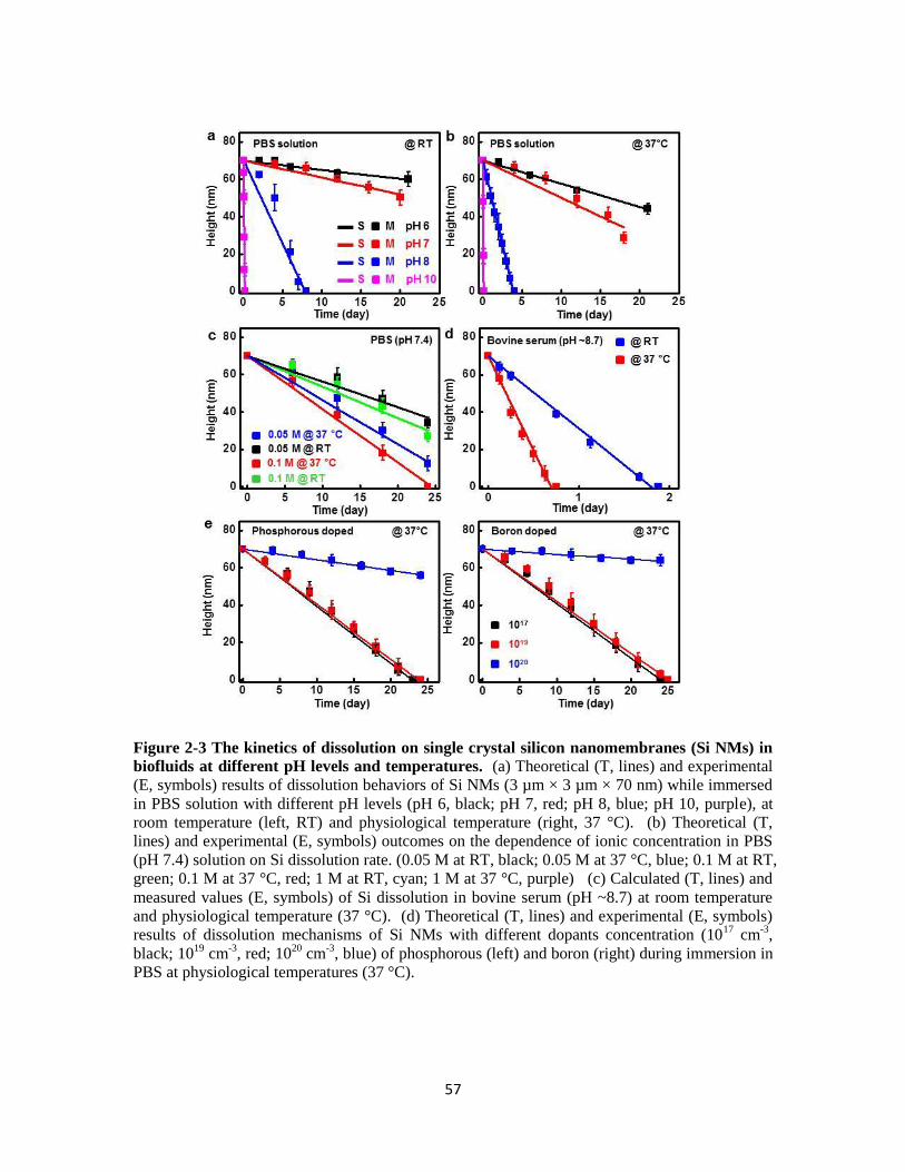
57
Figure 2-3 The kinetics of dissolution on single crystal silicon nanomembranes (Si NMs) in
biofluids at different pH levels and temperatures. (a) Theoretical (T, lines) and experimental
(E, symbols) results of dissolution behaviors of Si NMs (3 µm × 3 µm × 70 nm) while immersed
in PBS solution with different pH levels (pH 6, black; pH 7, red; pH 8, blue; pH 10, purple), at
room temperature (left, RT) and physiological temperature (right, 37 °C). (b) Theoretical (T,
lines) and experimental (E, symbols) outcomes on the dependence of ionic concentration in PBS
(pH 7.4) solution on Si dissolution rate. (0.05 M at RT, black; 0.05 M at 37 °C, blue; 0.1 M at RT,
green; 0.1 M at 37 °C, red; 1 M at RT, cyan; 1 M at 37 °C, purple) (c) Calculated (T, lines) and
measured values (E, symbols) of Si dissolution in bovine serum (pH ~8.7) at room temperature
and physiological temperature (37 °C). (d) Theoretical (T, lines) and experimental (E, symbols)
results of dissolution mechanisms of Si NMs with different dopants concentration (1017
cm-3
,
black; 1019
cm-3
, red; 1020
cm-3
, blue) of phosphorous (left) and boron (right) during immersion in
PBS at physiological temperatures (37 °C).

58
Figure 2-4 a, Theoretical model (lines) and experimental data (dots) of silicon dissolution
behaviors in PBS solution with different pH levels (pH 12 to 14), at different temperatures, RT
(left), 37 °C (right). pH 12 (black), pH 13 (red) and pH 14 (blue). on the effect of dopants
concentration, phosphorous (left) and boron (right). b, Theoretical and measured dissolution rate
of silicon as a function of pH level.

59
Figure 2-5 Theoretical model (lines) and experimental data (dots) of silicon dissolution rate in
various solutions, a, sea water (blue) and tap water (red) at RT, b, PBS solution (pH 7.4, 0.1 M, at
RT), with exposure to UV (blue) and daylight (red).

60
Figure 2-6 a, Theoretical model (lines) and experimental data (dots) on the effect of dopants
concentration, phosphorous (left) and boron (right). b, Dopant concentrations measured by
secondary ion mass spectrometry (SIMS), phosphorous (left) and boron (right).

61
Figure 2-7 Atomic force micrograph (AFM) topological images and scanning profiles of Si NMs
(initial dimension: 3 µm × 3 µm × 70 nm) at the time sequence during hydrolysis in (a), (b)
bovine serum (pH 8.7) at 37 °C and (c), (d) sea water at room temperature.
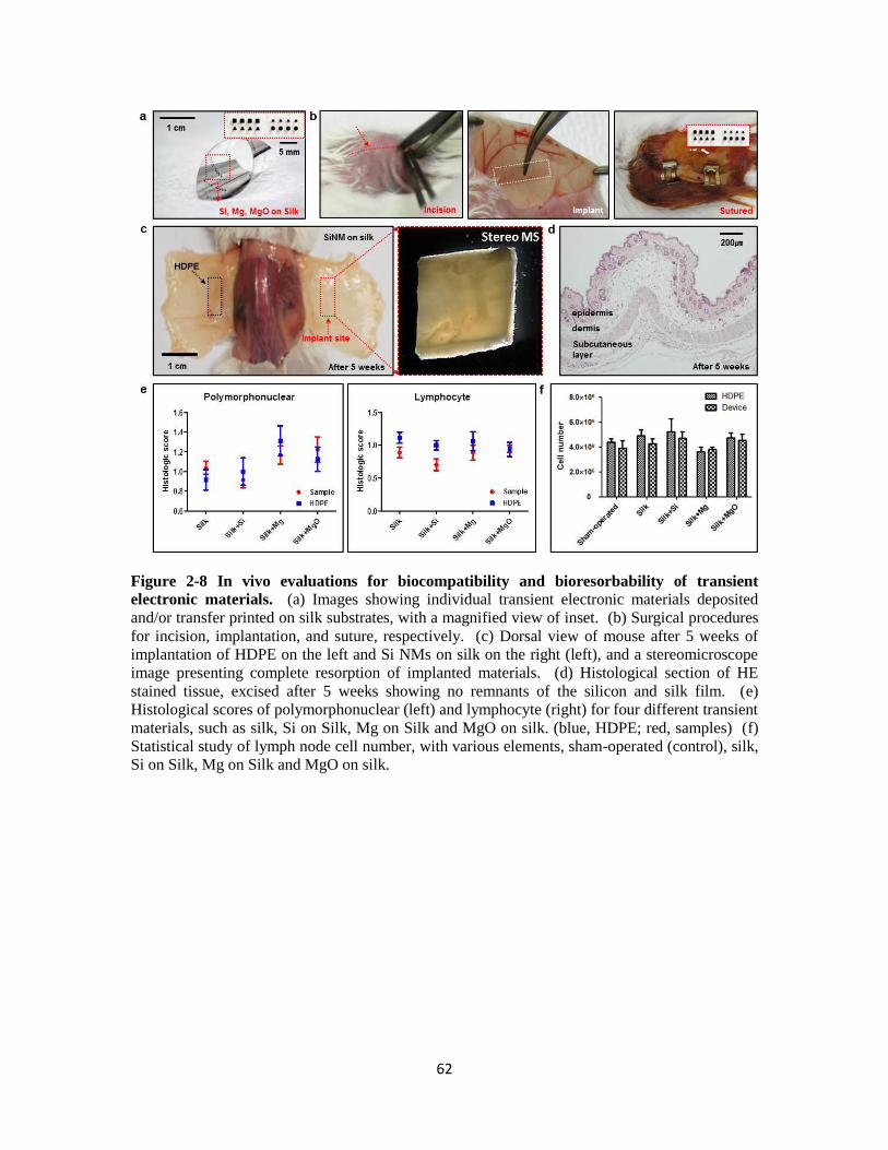
62
Figure 2-8 In vivo evaluations for biocompatibility and bioresorbability of transient
electronic materials. (a) Images showing individual transient electronic materials deposited
and/or transfer printed on silk substrates, with a magnified view of inset. (b) Surgical procedures
for incision, implantation, and suture, respectively. (c) Dorsal view of mouse after 5 weeks of
implantation of HDPE on the left and Si NMs on silk on the right (left), and a stereomicroscope
image presenting complete resorption of implanted materials. (d) Histological section of HE
stained tissue, excised after 5 weeks showing no remnants of the silicon and silk film. (e)
Histological scores of polymorphonuclear (left) and lymphocyte (right) for four different transient
materials, such as silk, Si on Silk, Mg on Silk and MgO on silk. (blue, HDPE; red, samples) (f)
Statistical study of lymph node cell number, with various elements, sham-operated (control), silk,
Si on Silk, Mg on Silk and MgO on silk.

63
Figure 2-9 a, Images of implantation procedure for in vivo evaluations. b, Implant site after 5
weeks.
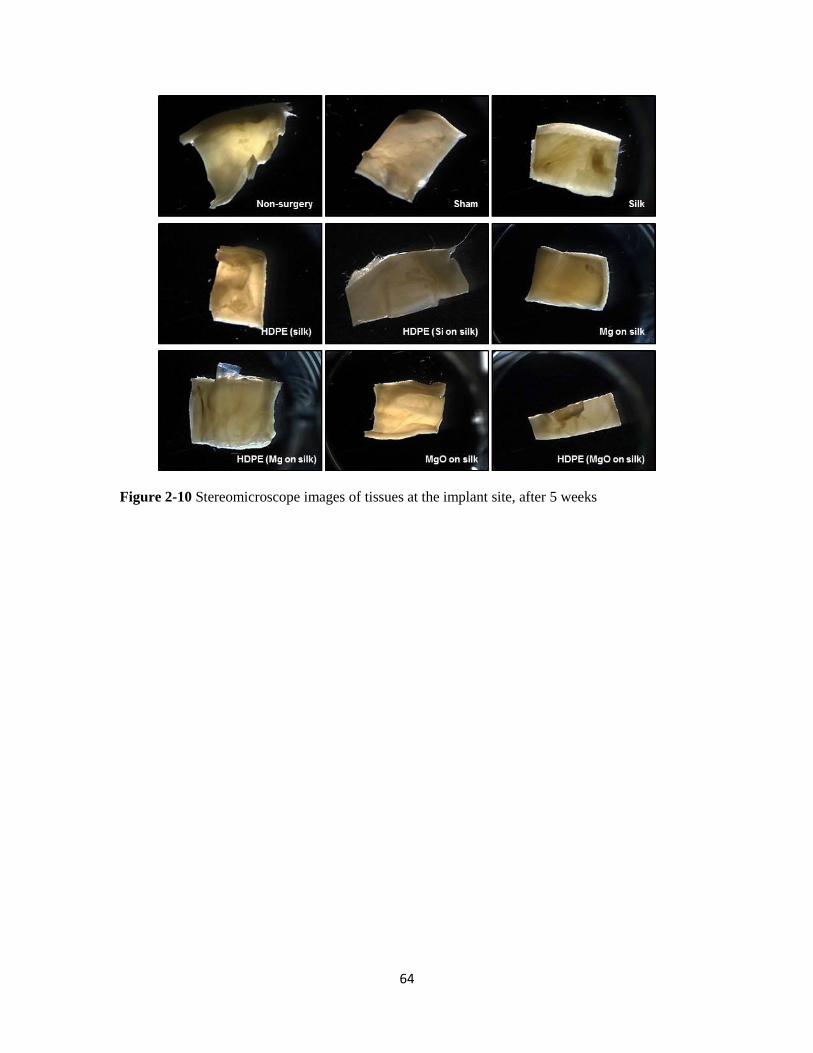
64
Figure 2-10 Stereomicroscope images of tissues at the implant site, after 5 weeks

65
Figure 2-11 Optical micrographs of HE-staining slices at the implant sites after 5 weeks.

66
Figure 2-12 Histological scores of individual materials after 5-week subcutaneous implantation.
(a) plasma cells (b) fibrosis
67
CHAPTER 3
2MATERIALS FOR BIORESORBABLE RADIO FREQUENCY ELECTRONICS
3.1 Introduction
Devices constructed using bioresorbable materials have many roles in clinical medicine,
ranging from drug delivery vehicles [1, 2] to stents [3, 4] and sutures [5, 6]. In such cases, the
function is defined primarily by the mechanics and/or the structure of the component, with
operation that is often passive. The ability to achieve similar bioresorbable characteristics in
active semiconductor devices and sensors could significantly expand the possible modes of use.
Past approaches include partially resorbable systems based on miniaturized silicon transistors
bonded to biomaterial substrates and, in separate work, on organic active materials (e.g.
semiconductors) [7-11]. Recent studies demonstrate a completely water soluble class of silicon-
based technology [12], to enable devices and systems that build on foundational knowledge and
engineering capabilities derived from the traditional integrated circuit industry. Components of
this type can be implanted into the human body where they gradually dissolve into biofluids after
their useful functional life, thereby eliminating unnecessary device load without the need for
surgical extraction. For many applications, radio frequency (RF) operation is a key feature, both
for data transmission and for power supply. The results presented here represent progress in this
direction. We report antennas, rectifying diodes, transistors, capacitors, inductors, resistors, ring
oscillators and RF energy harvesting sub-systems, all of which involve water soluble and
biocompatible constituent materials, i.e. silicon nanomembranes (Si NMs; semiconductors),
magnesium (Mg; conductors), silicon dioxide or magnesium oxide (SiO2 or MgO; interlayer
dielectrics), and silk (substrates).
2 Reprinted, by permission [Adv. Mater. 25, 3526-3531] Copyright © 2013 WILEY-VCH Verlag GmbH &
Co. KGaA, Weinheim

68
3.2 Experiments
The fabrication of passive components, such as capacitors and inductors begins as
follows. Mg electrodes (~200 nm) for bottom contacts (capacitors) and crossovers (inductors)
were formed by electron beam evaporation on a silk substrate. Deposition of MgO (~900 nm)
defined interlayer dielectrics. Another layer of Mg served as top electrodes for capacitors (~1
µm), and planar spiral coils for inductors (~3 µm). In all cases, high resolution stencil masks
made of polyimide (PI) films (Kapton, 12.5 µm, Dupont, USA) were used to pattern the Mg and
MgO.
Transient silicon CMOS ringoscillaotr starts three different doping procedures performed
on an n-type SOI wafer (SOITEC, France). Boron doping at 550 °C using spin-on dopant (SOD,
Filmtronics, USA) defined lightly doped regions for the p-wells (p-). Heavily doped p-type
regions for source and drain electrodes were formed at 1050 °C for p-type transistors.
Phosphorous doping at 950 °C defined highly doped areas for source and drain contacts for n-
type transistors. These doped silicon nanomembranes (Si NMs) were isolated by reactive ion
etching (RIE; Plasmatherm) with sulfur hexafluoride (SF6) gas. To release the Si NMs from the
SOI, the buried oxide was partially removed by wet etching with hydrofluoric acid (HF, 49%
electronic grade, ScienceLab, USA). Next, patterning a layer of photoresist (AZ 5214) formed
structures that anchored the Si NMs to the underlying wafer during a second etching step to
complete the removal of the buried oxide. Individual Si NMs formed by this procedure were
transfer printed onto a temporary “carrier” substrate coated with a layer of silk. Gate dielectrics
(MgO, ~80 nm), as well as electrodes and interconnects (Mg, ~300 nm) were deposited by
electron-beam evaporation through fine-line stencil masks.
In order to fabricate RF scavenging system, high temperature diffusion doping of boron
at ~1050 °C and phosphorous at ~950 °C using spin-on dopant established desired patterns of
doping in the top silicon layer of a silicon-on-insulator (SOI, SOITEC, France) substrate.

69
Thermally grown oxide (~1100 °C) served as the doping mask. Removal of the buried oxide
layer (~1 µm) with HF, released doped Si NMs (thickness ~300 nm, p-type), for transfer printing
onto a carrier wafer coated with poly (methylmethacrylate) (PMMA, ~100 nm; sacrificial) and
polyimide (PI, ~1.2 µm; cured at 250 °C for 1 hour in a glove box). Active device regions were
isolated by RIE with SF6 gas. The first layer of electrodes/interconnects was defined by lift-off
using LOR 20B (Microchem, USA) and AZ 5214 photoresists, with Mg (150 nm) deposited by
electron beam evaporation. A 900 nm thick layer of SiO2 was deposited by plasma-enhanced
chemical-vapor deposition (PECVD). Openings to the contacts were formed by buffered oxide
etching (BOE, 6:1, Transene company, USA) of the SiO2. Photolithography (AZ nLOF 2070,
Microchem, USA) and liftoff with a thick film of Mg (~3 µm) defined the second layer of
electrodes/interconnects. Next, an oxygen RIE (March) step created an open mesh pattern in the
PI to allow removal of the PMMA by immersion in acetone. Entire devices released in this
manner were then transfer printed onto a film of silk.
RF passive component was measured for scattering (S-) parameters using an Agilent
E8364A performance network analyzer. An external DC power supply was applied to the diodes
using a bias-tee during testing. The measurement setup was calibrated to the probe tips using a
standard Short-Open-Load-Thru (SOLT) on-wafer probing kit for a frequency range of 45 MHz -
20 GHz. Aglilent Advanced Design System (ADS) was used to extract device model parameters
from the respective equvilent circuits. The antennas were connected to SubMiniature - A (SMA)
connectors with silver epoxy. Their impedance characteristics were measured using an Agilent
5062A network analyzer with 1-port Open-Short-Load calibration.
3.3 Results and discussion
One of the most critical, but simplest, elements in RF systems for wireless reception /
transmission is in the antenna. Transient antennas can be formed by evaporation of Mg (500 nm)
through stencil masks made of polyimide (PI) films (Kapton, 12.5 µm, Dupont, USA) on thin

70
films of silk. Two designs form the focus of studies reported here: simple linear dipoles
consisting of two quarter wavelength arms and wideband quasi log-periodic dipoles, designed to
operate at ~2.4 GHz and ~950 MHz, respectively. Figure 3-1a presents images of a transient Mg
antenna at a sequence of times during immersion in deionized (DI) water at room temperature.
The Mg and silk completely disappear after ~2 hours by hydrolysis and simple dissolution,
respectively. An alternative route to similar antennas, but with thicknesses that can be much
larger than the skin depth at relevant RF frequencies, exploits Mg foils (thickness from 5 µm to
50 µm, purity of 99.9 %, Goodfellow, UK) cut into appropriate shapes. A layer of solvent-
perfused silk serves as an adhesive to bond such antennas to silk substrates (Figure 3-2a). The
measured S-parameters in Figure 3-1b show that both antennas are well matched to their designed
operating frequencies. Images of the devices with coaxial connectors appear in Figure 3-3.
Figure 3-2b shows a 950 MHz antenna integrated with a commercial RF power scavenging
system on a printed circuit board to demonstrate functionality. Additional details can be found in
Figure 3-2c.
Various transient components with passive RF function, such as capacitors, inductors,
and resistors, are also essential. Figure 3-1, c to g, provides images and electrical properties of
several such components. As an example, a simple transient resistor consisting of a serpentine
trace of Mg (Figure 3-1c) formed by evaporation onto silk through a stencil mask, indicates a
resistance of 100 ohm, suitable for use in RF current-limiters and voltage dividers, as examples.
Capacitors and inductors can be formed on silk in which MgO (900 nm thick, formed by electron
beam evaporation) serves as the dielectric, and Mg forms the electrodes and conducting traces.
(Details appear in the experimental section.) The capacitors explored here exploit simple, parallel
plate geometries with various lateral dimensions (Figure 3-1d; 150 µm × 150 um (black), 250 µm
× 250 µm (red), 400 µm × 400 µm (blue) and 550 µm × 550 µm (green)). Measured capacitances
and Q factors of each capacitor appear in Figure 3-1e, along with simulation results. The
operating frequencies extend up to ~6 GHz. Simple inductors (Figure 3-1f) can be built using
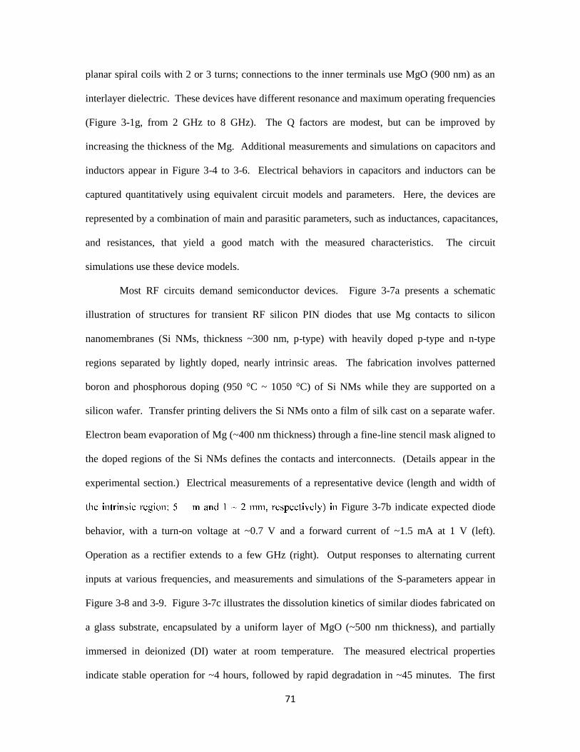
71
planar spiral coils with 2 or 3 turns; connections to the inner terminals use MgO (900 nm) as an
interlayer dielectric. These devices have different resonance and maximum operating frequencies
(Figure 3-1g, from 2 GHz to 8 GHz). The Q factors are modest, but can be improved by
increasing the thickness of the Mg. Additional measurements and simulations on capacitors and
inductors appear in Figure 3-4 to 3-6. Electrical behaviors in capacitors and inductors can be
captured quantitatively using equivalent circuit models and parameters. Here, the devices are
represented by a combination of main and parasitic parameters, such as inductances, capacitances,
and resistances, that yield a good match with the measured characteristics. The circuit
simulations use these device models.
Most RF circuits demand semiconductor devices. Figure 3-7a presents a schematic
illustration of structures for transient RF silicon PIN diodes that use Mg contacts to silicon
nanomembranes (Si NMs, thickness ~300 nm, p-type) with heavily doped p-type and n-type
regions separated by lightly doped, nearly intrinsic areas. The fabrication involves patterned
boron and phosphorous doping (950 °C ~ 1050 °C) of Si NMs while they are supported on a
silicon wafer. Transfer printing delivers the Si NMs onto a film of silk cast on a separate wafer.
Electron beam evaporation of Mg (~400 nm thickness) through a fine-line stencil mask aligned to
the doped regions of the Si NMs defines the contacts and interconnects. (Details appear in the
experimental section.) Electrical measurements of a representative device (length and width of
Figure 3-7b indicate expected diode
behavior, with a turn-on voltage at ~0.7 V and a forward current of ~1.5 mA at 1 V (left).
Operation as a rectifier extends to a few GHz (right). Output responses to alternating current
inputs at various frequencies, and measurements and simulations of the S-parameters appear in
Figure 3-8 and 3-9. Figure 3-7c illustrates the dissolution kinetics of similar diodes fabricated on
a glass substrate, encapsulated by a uniform layer of MgO (~500 nm thickness), and partially
immersed in deionized (DI) water at room temperature. The measured electrical properties
indicate stable operation for ~4 hours, followed by rapid degradation in ~45 minutes. The first

72
stage of this kinetics depends on dissolution of the MgO encapsulant and/or permeation through it;
the second depends mainly on hydrolysis of the Mg electrodes. The thickness of the MgO can be
selected to define the first time scale, in a way that does not affect device performance. Other
encapsulating materials can be considered for times that extend beyond those practically
accessible with MgO [12].
RF transistors enable active functionality. To demonstrate possibilities in transient RF,
we constructed three-stage complementary metal-oxide-semiconductor (CMOS) ring oscillators
using transient n-channel and p-channel metal-oxide-semiconductor field-effect transistors
(MOSFETs) based on Si NMs, with Mg (~250 nm) for source, drain, gate contacts and
interconnects, and MgO (~80 nm) for the gate dielectrics. Figure 3-10a provides an illustration
and a schematic circuit diagram. To enable both n- and p-channel MOSFETs in a single Si NM,
high temperature diffusion procedures create lightly doped p-wells (p-), and highly doped source
and drain contacts for each MOSFET (n+, p
+). Source and drain electrodes formed next to the p-
wells define p-channel MOSFETs. Heavily doped regions for source and drain regions inside the
p-wells enable contacts for n-channel MOSFETs. (See details in experimental section.) Figure 3-
10b and c represent transfer curves and full current-voltage characteristics measured from p-
channel and n-channel devices, respectively. Optical microscope images appear in the insets. In
both types of MOSFETs, the on/off current ratios (Ion/Ioff) are ~105. The mobilities are ~70
cm2/V·s and ~350 cm
2/V·s, for the p- and n-channel cases, respectively. Measurements on a
typical CMOS inverter appear in Figure 3-10d; the gain and threshold voltage (Vth) are ~60 and -
1 V, respectively. The negative threshold voltage of the inverters results mainly from the high
negative threshold voltage (~5 V) of the p-channel MOSFETs. Figure 3-10e shows time-domain
output voltage characteristics of a ring oscillator. The operating frequency can be adjusted, up to
~4.1 MHz, with applied bias, 10 V (black), 15 V (red), 20 V (blue). Theoretically, this frequency
is inversely proportional to the number of stages (N) and linearly proportional to the applied
voltage (Vdd). In the absence of other factors, the relative slope is expected to be approximately 1.

73
Deviations from this behavior suggest some non-idealities, likely due to propagation delays and
parasitic capacitances [13, 14].
The various transient RF electronic devices described previously can be integrated
together for higher levels of functionality. A transient wireless RF power scavenger circuit
provides a good example (Figure 3-11). The circuit contains an RF antenna, an inductor, six
capacitors, a resistor and eight diodes, as shown in Figure 3-11a and b. A circuit diagram appears
in Figure 3-11c. In this case, a thin layer of polyimide provides mechanical support to facilitate
transfer of the entire, interconnected system (except for the antenna) to silk at improved yields.
Connecting the input of the system to an RF function generator and the output to a commercial
LED indicates effective rectification, over a frequency range from 10 kHz to 950 MHz (Figure 3-
11d). Additional data appear in Figure 3-9e. By connecting the circuit to a Mg antenna designed
for operation at 950 MHz, the system can wirelessly harvest energy from an RF transmitter, to
turn on a LED at a distance of ~2 meters, as shown in Figure 3-11e. The power received by the
antenna is approximately 17.3 dBm (54 mW) and the LED consumes a power of 8.5 mW. The
resulting power conversion efficiency (PCE) is determined to be -8 dB (15.7%). This value is
somewhat smaller than those of commercial bridge rectifiers, which range from 26.5% to 37%,
due to their use of optimized fabrication processes and materials [15-17]. Systems based on half-
wave rectification circuits can also power LEDs, but with reduced efficiencies compared to the
case of the full-wave rectifier (Figure 3-12). Circuits designed to enable integration with Si
CMOS ring oscillators powered by scavenging circuits appear in Figure 3-13. In all examples,
the electronic materials are water-soluble/biodegradable. Figure 3-11f shows a set of images
collected at different times during dissolution. The entire power scavenger initially disintegrates
in DI water at room temperature due to dissolution of the silk substrate; subsequently, the
remaining materials reactively dissolve at their respective rates. A thick layer of Mg (~3 µm)
requires some days to dissolve. At these neutral pH levels, the Si and SiO2 dissolve at rates that
are much slower than those at physiological conditions [12].
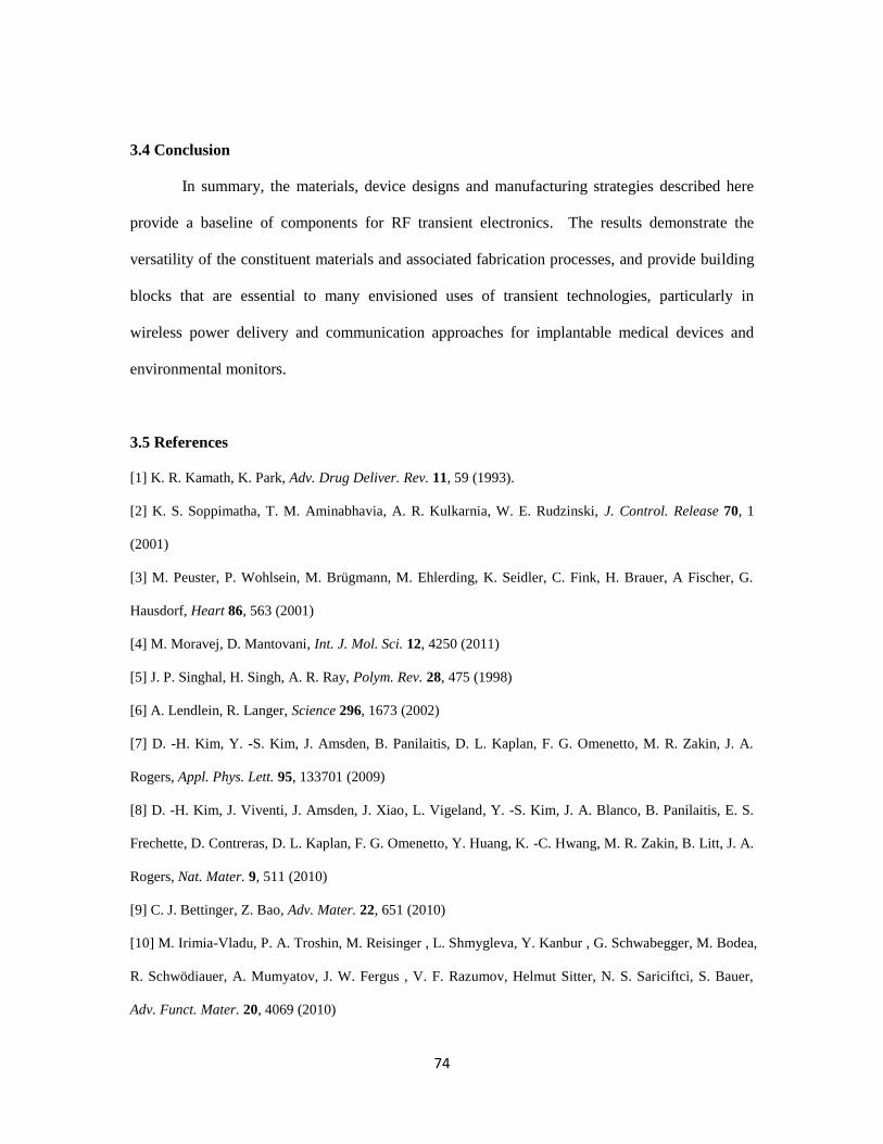
74
3.4 Conclusion
In summary, the materials, device designs and manufacturing strategies described here
provide a baseline of components for RF transient electronics. The results demonstrate the
versatility of the constituent materials and associated fabrication processes, and provide building
blocks that are essential to many envisioned uses of transient technologies, particularly in
wireless power delivery and communication approaches for implantable medical devices and
environmental monitors.
3.5 References
[1] K. R. Kamath, K. Park, Adv. Drug Deliver. Rev. 11, 59 (1993).
[2] K. S. Soppimatha, T. M. Aminabhavia, A. R. Kulkarnia, W. E. Rudzinski, J. Control. Release 70, 1
(2001)
[3] M. Peuster, P. Wohlsein, M. Brügmann, M. Ehlerding, K. Seidler, C. Fink, H. Brauer, A Fischer, G.
Hausdorf, Heart 86, 563 (2001)
[4] M. Moravej, D. Mantovani, Int. J. Mol. Sci. 12, 4250 (2011)
[5] J. P. Singhal, H. Singh, A. R. Ray, Polym. Rev. 28, 475 (1998)
[6] A. Lendlein, R. Langer, Science 296, 1673 (2002)
[7] D. -H. Kim, Y. -S. Kim, J. Amsden, B. Panilaitis, D. L. Kaplan, F. G. Omenetto, M. R. Zakin, J. A.
Rogers, Appl. Phys. Lett. 95, 133701 (2009)
[8] D. -H. Kim, J. Viventi, J. Amsden, J. Xiao, L. Vigeland, Y. -S. Kim, J. A. Blanco, B. Panilaitis, E. S.
Frechette, D. Contreras, D. L. Kaplan, F. G. Omenetto, Y. Huang, K. -C. Hwang, M. R. Zakin, B. Litt, J. A.
Rogers, Nat. Mater. 9, 511 (2010)
[9] C. J. Bettinger, Z. Bao, Adv. Mater. 22, 651 (2010)
[10] M. Irimia-Vladu, P. A. Troshin, M. Reisinger , L. Shmygleva, Y. Kanbur , G. Schwabegger, M. Bodea,
R. Schwödiauer, A. Mumyatov, J. W. Fergus , V. F. Razumov, Helmut Sitter, N. S. Sariciftci, S. Bauer,
Adv. Funct. Mater. 20, 4069 (2010)

75
[11] C. Legnani, C. Vilani, V. L. Calil, H. S. Barud, W. G. Quirino, C. A. Achete, S. J. L. Ribeiro, M.
Cremona, Thin Solid Films 517, 1016 (2008)
[12] S. -W. Hwang, H. Tao, D. -H. Kim, H. Cheng, J. -K. Song, E. Rill, M. A. Brenckle, B. Panilaitis, S. M.
Won, Y. -S. Kim, Y. M. Song, K. J. Yu, A. Ameen, R. Li, Y. Su, M. Yang, D. L. Kaplan, M. R. Zakin, M.
J. Slepian, Y. Huang, F. G. Omenetto, J. A. Rogers, Science 337, 1640 (2012)
[13] M. K. Mandal, B. C. Sarkar, Indian J. Pure Ap. Phy. 48, 136 (2010)
[14] V. Michal, Radioelektronika 2012 22nd International Conference 1 (2012)
[15] J. Yi, W.-H. Ki, C.-Y. Tsui, IEEE T. Circuits Syst. 54, 153 (2007)
[16] P. T. Theilmann, C. D. Presti, D. Kelly, P. M. Asbeck, Proc. IEEE Radio Frequency Integrated
Circuits Symp. 105 (2010)
[17] P. T. Theilmann, C. D. Presti, D. J. Kelly, P. M. Asbeck, IEEE T. Circuits Syst. 59, 2111 (2012)
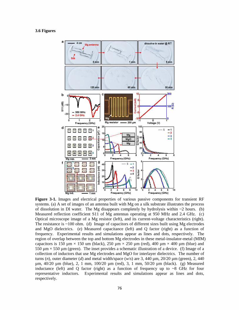
76
3.6 Figures
Figure 3-1. Images and electrical properties of various passive components for transient RF
systems. (a) A set of images of an antenna built with Mg on a silk substrate illustrates the process
of dissolution in DI water. The Mg disappears completely by hydrolysis within ~2 hours. (b)
Measured reflection coefficient S11 of Mg antennas operating at 950 MHz and 2.4 GHz. (c)
Optical microscope image of a Mg resistor (left), and its current-voltage characteristics (right).
The resistance is ~100 ohm. (d) Image of capacitors of different sizes built using Mg electrodes
and MgO dielectrics. (e) Measured capacitance (left) and Q factor (right) as a function of
frequency. Experimental results and simulations appear as lines and dots, respectively. The
region of overlap between the top and bottom Mg electrodes in these metal-insulator-metal (MIM)
capacitors is 150 µm × 150 um (black), 250 µm × 250 µm (red), 400 µm × 400 µm (blue) and
550 µm × 550 µm (green). The inset provides a schematic illustration of a device. (f) Image of a
collection of inductors that use Mg electrodes and MgO for interlayer dielectrics. The number of
turns (n), outer diameter (d) and metal width/space (w/s) are 3, 440 µm, 20/20 µm (green), 2, 440
µm, 40/20 µm (blue), 2, 1 mm, 100/20 µm (red), 3, 1 mm, 50/20 µm (black). (g) Measured
inductance (left) and Q factor (right) as a function of frequency up to ~8 GHz for four
representative inductors. Experimental results and simulations appear as lines and dots,
respectively.
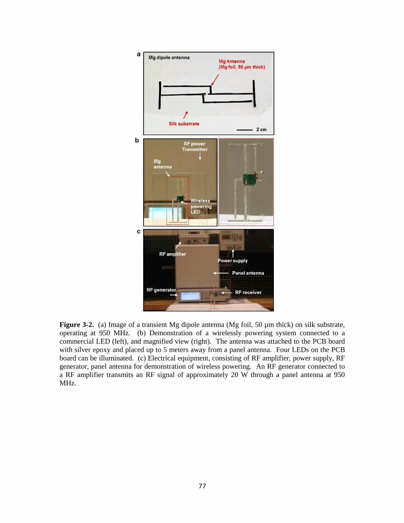
77
Figure 3-2. (a) Image of a transient Mg dipole antenna (Mg foil, 50 µm thick) on silk substrate,
operating at 950 MHz. (b) Demonstration of a wirelessly powering system connected to a
commercial LED (left), and magnified view (right). The antenna was attached to the PCB board
with silver epoxy and placed up to 5 meters away from a panel antenna. Four LEDs on the PCB
board can be illuminated. (c) Electrical equipment, consisting of RF amplifier, power supply, RF
generator, panel antenna for demonstration of wireless powering. An RF generator connected to
a RF amplifier transmits an RF signal of approximately 20 W through a panel antenna at 950
MHz.

78
Figure 3-3. Images and measured properties of transient CMOS inverters and ring oscillators. (a)
Image of CMOS three-stage ring oscillators (left), and circuit diagram (right). (b) SQRT (red)
and log scale (blue) transfer curves of a typical transient p-channel MOSFET. The channel length
(L) and width (W) are 5 µm and 300 µm, respectively. The mobility and on/off ratio are ~70
cm2/V·s and ~10
5, respectively. The inset shows a microscope image of a representative device.
(c) I-V characteristics of a typical n-channel MOSFET. The channel length (L) and width (W)
are 15 µm and 100 µm, respectively. The mobility and on/off ratio are 400 cm2/V·s and ~10
5,
respectively. All MOSFETs use Mg for source, drain and gate electrodes, and MgO for the gate
dielectric. (d) Output voltage characteristics of a representative CMOS inverter with Vdd = 10 V.
The voltage gain is ~60. An optical microscope image appears in the inset. (e) Measured time
domain responses of a ring oscillator at different frequencies.
79
Figure 3-4. Transient RF power scavenging circuits, and integration with a transient antenna. (a)
Image of transient full-wave rectifying circuit that includes an array of diodes and capacitors, an
inductor, a resistor and antenna pads, all fabricated with transient electronic materials: Si NMs
(semiconductors), Mg (electrodes), SiO2 (interlayer dielectrics), and silk (substrates). (b)
Schematic exploded view illustration. (c) Circuit diagram. (d) Operational demonstration of a
full wave rectifying circuit with a commercial LED. (e) Image of a full wave rectifying system
powered wirelessly with an RF transmitter and a Mg receiving antenna (left), and magnified view
(right). The working distance here is ~2 meters. (f) Images of a rectifying circuit immersed in
deionized water after 1 min, 2 min, 5 min and 1 hour, respectively.

80
Figure 3-5. Measured (lines) and simulated (dots) results for capacitors plotted on a Smith chart
from 45 MHz to 10 GHz. Each number indicates a different size of capacitor, as shown in Figure
3-1d. Red and blue lines describe S12/S21 and S11/S22, respectively.

81
Figure 3-6. Measured (lines) and simulated (dots) results for inductors plotted on a Smith chart
from 45 MHz to 15 GHz. The individual chart shows different inductors as described in Figure
3-1f. Red and blue lines indicate S12/S21 and S11/S22, respectively.

82
Figure 3-7. Electrical measurements of transient diodes, and dissolution kinetics of a
representative diode and antenna. (a) Schematic illustration of Si NM PIN diodes (rectifiers)
fabricated with Mg electrodes on a silk substrate. The near intrinsic “i” region has dimensions of
~5 µm × 1 ~ 2 mm. (b) Current-voltage characteristics of a representative diode (left), including
an image in the inset, and measured values (lines) and simulations (dots) of the S21 scattering
parameter at frequencies up to 10 GHz with different DC biases (right). (c) Measurements of
dissolution kinetics of a diode encapsulated with MgO (~500 nm). The results show stable
current output for ~4 hours, followed by rapid degraded over the following ~45 min. due to
dissolution of the Mg electrodes.

83
Figure 3-8. (a) Measurements (lines) and simulations (dots) of S11 and S22 parameters of Si
diodes at frequencies up to 10 GHz with different DC biases. (b) Measured (lines) and simulated
results (dots) for a Si diode with various DC biases plotted on a Smith chart from 45 MHz to 10
GHz.
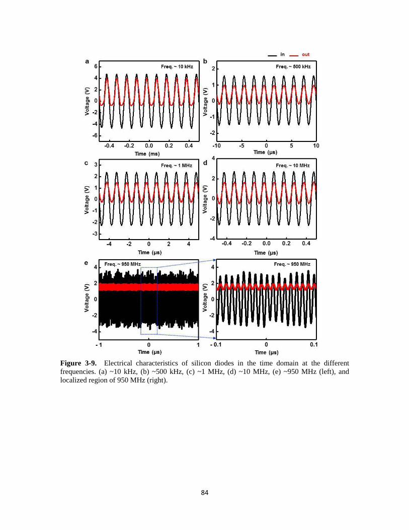
84
Figure 3-9. Electrical characteristics of silicon diodes in the time domain at the different
frequencies. (a) ~10 kHz, (b) ~500 kHz, (c) ~1 MHz, (d) ~10 MHz, (e) ~950 MHz (left), and
localized region of 950 MHz (right).

85
Figure 3-10. Images of transient Mg antennas operating at different frequencies. (a) ~950 MHz
wideband dipole, (b) ~2.4 GHz linear dipole.

86
Figure 3-11. Experimental results (lines) and simulations (dots) of the S-parameters of
capacitors and inductors. (a) S11 and S22, (b) S12 and S21 values for capacitors of different
sizes as a function of frequency up to 10 GHz. (c) S11 and S22, (d) S12 and S21 values for
inductors with various designs as a function of frequency up to 15 GHz.

87
Figure 3-12. (a) Image of a transient half-wave rectifier that includes Si diodes, inductors,
capacitors, a resistor and antenna pads. (b) System demonstration with a commercial LED. (c)
Schematic circuit diagram. (d) Demonstration of wireless powering using a half-wave rectifying
system with a Mg antenna at a distance of ~1 meter (left), and magnified view (right).
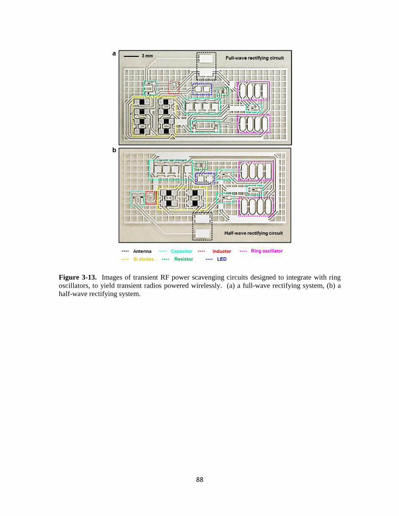
88
Figure 3-13. Images of transient RF power scavenging circuits designed to integrate with ring
oscillators, to yield transient radios powered wirelessly. (a) a full-wave rectifying system, (b) a
half-wave rectifying system.
89
CHAPTER 4
3MATERIALS AND PROCESSES FOR TRANSIENT AND BIORESORBABLE HIGH
PERFORMANCE ELECTRONICS
4.1 Introduction
Implantable biomedical components serve critically important roles in modern clinical
medicine. Such devices can be classified into two types: those that exist for long periods of time,
typically designed to be permanent; and those that disappear, or resorb, in the body after they
provide some useful function. The former includes both simple, passive devices such as artificial
joints and pins [1], as well as sophisticated electronic components such as deep brain electrical
stimulators [2], cardiac pacemakers [3] and programmable drug delivery systems [4]. The latter,
by contrast, is currently available only in the form of passive elements such as resorbable sutures
[5, 6] or matrices for drug release [7, 8], degradable intravascular stents [9, 10] and resorbable
plate-screw systems [11]. An unaddressed technology opportunity, then, exists in biodegradable
devices that are capable of active electronic processing, sensing, communication and/or actuation
within or on the surface of the body. Envisioned uses range from non-antibiotic appliques
designed to reduce the incidence of surgical site infections, to electrical stimulators that can
accelerate bone growth, to systems that can release drugs at programmed intervals. In each case,
the devices operate only over some finite period of time, typically defined by a healing process;
afterward, they resorb to eliminate unnecessary device load in a way that avoids surgical
intervention.
Initial, early technical work toward this type of technology yielded two examples of
partially resorbable devices, in the sense that certain, but not all, of the component materials
3 Reprinted, by permission [DOI: 10.1002/adfm.201300127] Copyright © 2013 WILEY-VCH Verlag
GmbH & Co. KGaA, Weinheim

90
resorb. One involves ultrathin electrodes and/or transistors built on films of silk fibroin,
engineered to facilitate conformal contact with biological tissues, as demonstrated in
electrocorticography [12], and to disperse thin, miniaturized electronic components in ways that
minimize adverse body responses, as demonstrated in sub-dermal implants [13]. The other uses
organic or bio-organic semiconductors with polymer dielectrics/substrates to yield systems in
which all components except for the electrodes and interconnects dissolve in bio-fluids, in a
potentially biocompatible manner [14, 15]. Although the modest properties of known organic
electronic materials limit the performance that can be achieved, this approach has some potential
for devices that require only simple functions. A recent report describes materials and schemes
that bypass constraints associated with these two previous directions [16]. The result is a fully
resorbable, high performance class of electronics, where ultrathin sheets of semiconductor-grade
monocrystalline silicon (i.e. silicon nanomembranes, or Si-NMs) serve as the active materials,
inorganic dielectrics (e.g. MgO, SiO2) and conventional metals (e.g. Mg) provide the other
electronic functions, and silk forms the substrate and encapsulation layers. Enabled devices
encompass nearly all of the key building blocks for integrated circuits, ranging from metal-oxide
semiconductor field-effect transistors (MOSFETs) to pn junction diodes, resistors, inductors,
capacitors. Additional demonstrated components include solar cells, photodetectors, strain and
temperature gauges, inductive power delivery systems and others. Although initially conceived
for bioresorbable devices and demonstrated in programmable non-antibiotic bacteriocidal
appliqués, this same technology can be more generally considered as a physically transient form
of electronics, capable of disappearing via controlled physical or chemical change with well-
defined rates. Non-biological applications include environmental sensors that avoid the need for
recovery and collection after use, and consumer devices that minimize costly and hazardous
disposal procedures.
A disadvantage of the original embodiment of this class of transient electronics is that many of
the fabrication steps were performed on a transient substrate (e.g. silk), thereby constraining

91
significantly the processing temperatures, choices of solvents and other aspects of the processing.
These limitations prevent the use of manufacturing techniques that are found in high volume, low
cost production of commercial silicon integrated circuits. The work described here establishes a
silicon wafer-based strategy to fully formed transient circuit components and circuits, in
configurations that allow their subsequent, and separate, integration with transient substrates and
packaging materials. The results are important because they have the potential to enable realistic
manufacturing strategies for transient electronics, in which only modest modifications to
microelectronic fabrication facilities are needed. The concepts rely on the combined use of a
specialized type of silicon on insulator (SOI) wafer and the techniques of transfer printing. The
resulting devices involve constituent materials that all have some solubility in water: silicon,
silicon dioxide, magnesium oxide, magnesium and silk. The following describes the concepts
and demonstrates their use in fabrication of various electronic components and simple logic gates,
with studies of their transient behaviors both through in vitro investigations of the kinetics and in
vivo evaluations of biocompatibility and resorption.
4.2 Experiments
The fabrication began with custom silicon-on-insulator (SOI, Silicon Quest Inc., USA)
wafers with a top silicon (100) layer (~2 µm thick, p-type 10-20 Ω·cm), a buried layer of silicon
dioxide (~1 µm thick) and a Si (111) supporting substrate. Repetitive cycles of dry oxidation at
1100 °C followed by wet chemical etching in hydrofluoric acid reduced the thickness of the top
silicon layer to ~100 nm. Patterned doping with phosphorous at ~950 °C using a spin-on dopant
(SOD, Filmtronics, USA) defined regions for source and drain contacts. Isolated areas of silicon
were defined by patterned reactive ion etching (RIE; Plasmatherm, USA) with sulfur hexafluoride
(SF6) gas for ~1 min. A thin layer of SiO2 (100 nm) deposited by plasma-enhanced chemical
vapor deposition (PECVD) served as the gate dielectric. Patterned wet-etching of this layer with
buffered oxide etchant (BOE, 6:1, Transcene company, USA) opened windows for source and

92
drain contacts. Photolithography and liftoff formed Mg electrodes (~200 nm) for source, drain
and gate contacts. An additional layer of PECVD SiO2 (100 nm) served as an encapsulant, with
openings to the contacts formed by BOE. A 400 nm thick, unpatterned layer of Si3N4 deposited
by PECVD passivated the entire area of the devices. A bilayer of Cr/Au (10/150 nm) deposited
by electron beam evaporation provided a hard mask for deep trench etching by RIE down to the
underlying Si (111) wafer through the buried oxide. These processed substrates were then
submerged in tetramethyl ammonium hydroxide (TMAH, 25 wt. % in H2O, Sigma-Aldrich, USA)
for ~30 min. at 100 °C for anisotropic undercut etching of the wafer. Removal of the metal hard
mask followed this etching. Next, the devices were transfer printed to a spin cast film of silk, and
the passivation layer of Si3N4 was removed by RIE. In the case of logic gates, such as NAND
and NOR gates, interconnection traces of Mg were deposited through fine-line stencil masks
(Kapton, 12.5 µm, Dupont, USA).
To observe dissolution of the constituent materials (Si, SiO2 and Mg), a collection of
undercut etched inverters on SOI were immersed in phosphate buffered saline (PBS, pH 7.4,
Sigma-aldrich, USA) solution at 37 °C. Optical microscope images revealed the various stages of
dissolution over the course of 4 weeks. Most of the Mg electrodes (~200nm) react with water to
form Mg(OH)2 within 12 hours; any residual remaining Mg dissappeared completely in 36 hours.
The exposed regions of Mg dissolved first, followed by undercut dissolution of those regions of
Mg that lie beneath PECVD SiO2. Simultaneously, the SiO2 (~100nm, interlayer dielectrics) also
began to dissolve to form Si(OH)4. Due to the elimination of the underlying Mg, much of this
SiO2 disintegrated into tiny pieces (not visible directly), thereby accelerating the elimination of
this layer. The SiO2 (~100 nm) that forms the gate dielectric disappeared in two weeks. Partial
dissolution of the Si occurred at the same time. Dissapearance of all materials except for the
buried oxide (SiO2, 1 µm) was complete within 4 weeks. Previous studies indicate that oxides
grown at high temperatures have slow dissolution rates due to their morphology/density [22].
93
Monitoring of electrical properties during dissolution was performed using transistors and
inverters encapsulated by a uniform layer of MgO (800 nm). These devices were completely
immersed in DI water, but configured with external probing pads to enable continuous
mesurement. Experimental results illustrate two-stage dissolution kinetics: stable device
operation, without changes in electrical characteristics, followed by comparatively fast
degradation in key performance parameters. The duration of the first stage depends on the rate of
dissolution of the encapsulation materials and/or penetration of water through them. The second
stage is determined, primarily, by relatively fast dissolution of the Mg electrodes.
4.3 Results and discussion
The overall scheme involves complete fabrication of circuits and/or circuit components in
transient materials on a silicon wafer, followed by their controlled release and subsequent
integration onto a transient substrate via transfer printing. Figure 4-1 presents exploded-view
schematic illustrations and optical micrographs of a representative system composed of a large-
scale array of transient n-channel monocrystalline silicon metal-oxide field-effect transistors
(MOSFETs), undercut etched from a SOI (111) wafer on which they were formed (Figure 4-1a)
and after their transfer to a thin sheet of silk as a substrate (Figure 4-1b). The SOI wafer consists
of ultrathin top layer of Si (p-type, ~100 nm) with (100) orientation for the active regions of the
devices, a buried oxide layer (~ 1 µm) and supporting wafer with (111) orientation. The
orientation of the wafer plays a critical role in the release of devices from its surface, as described
in the following. Fabrication begins with high temperature, patterned doping (phosphorous at
~950 °C) of the top Si to define the channel regions and contacts for the MOSFETs. Patterned
etching of the silicon creates isolated regions for each of the devices. A coating of SiO2 (~100
nm) deposited by plasma-enhanced chemical-vapor deposition (PECVD) at 250 °C forms the gate
dielectric. Etching in buffered oxide etchant (BOE, 6:1, Transene company, USA) create
windows for source and drain contacts. Depositing Mg (~200 nm) by electron beam evaporation

94
yields source, drain and gate electrodes aligned to the contacts and channel areas (Figure 4-2a).
Sequential PECVD steps define encapsulation layers of SiO2 (~100 nm thick; patterned to expose
the source, drain, and gate contacts) and Si3N4 (~400 nm thick; uniform across the entire area).
Deep etching through a hard mask of Cr/Au (10/200 nm) establish trenches between the devices,
down to a depth of ~1.5 µm into the (111) silicon supporting wafer (Figure 4-2b). Anisotropic
wet etching of the underlying (111) silicon with tetramethyl ammonium hydroxide (TMAH, 25
wt. % in H2O, Sigma-Aldrich, USA; 30 min at 100 °C) leaves free-standing MOSFETs tethered
to the wafer at their ends by bridging films of the buried oxide (Figure 4-2c). Cross-sectional
images in Figure 4-2d illustrate that the undercut proceeds in the (110) direction, along the
surface of the wafer, to allow efficient release. Details appear in Figure 4-3. Free-standing
MOSFETs created in this manner have total thicknesses of < 2 µm, including the buried oxide
layer (~1 µm). Because the SOI substrates and processing conditions are compatible with state-
of-the-art commercial microelectronics fabrication facilities, dramatic reductions in the
thicknesses and lateral dimensions are possible.
Figure 4-1b illustrates an array of such MOSFETs after release from the SOI substrate
and integration onto a film of silk, using the techniques of transfer printing [17]. A reactive ion
etching (RIE; SF6) step removes the Si3N4 after transfer. The buried SiO2 and top coating of
PECVD SiO2 physically isolate the devices from their surroundings, thereby enabling
performance that is nearly independent of substrate or subsequent encapsulating material. This
versatility is important, particularly in an area such as transient electronics where choices of
constituent materials can be highly unusual compared to those with proven utility in conventional
electronics. Figure 4-1c demonstrates that these types of MOSFETs can be fabricated and
transferred over large areas, with high yields.
Figure 4-4 provides a set of images collected during dissolution of a system like that
illustrated in Figure 4-1c, at various times after immersion in deionized (DI) water at room
temperature. Here, the silk rapidly dissolves within two minutes, thereby leading to

95
disintegration of the array into individual devices. (The rate of dissolution of silk can be
controlled over a wide range.) [18, 19] Each component then gradually disappears in a manner
defined by the dissolution rates of the various constituent materials [16]. Hydrolysis consumes the
Mg in several hours (Mg + 2H2O → Mg(OH)2 + H2). Dissolution of PECVD SiO2 and Si in PBS
solution (pH 7.4) at room temperature occurs on a timescale of weeks (SiO2 + 2H2O → Si(OH)4;
Si + 4H2O → Si(OH)4 + 2H2); the thermal oxide takes considerably longer. In all of the materials,
the rates for complete disappearance depend strongly on temperature, pH, layer thicknesses and
morphology.
The overall fabrication process accommodates not only individual MOSFETs, but also
logic gates and small-scale integrated circuits. Figure 4-5a shows an array of inverters, with a
magnified optical micrograph and a circuit diagram. Each inverter consists of a load and an input
transistor with channel lengths and widths of ~20 µm and ~10 µm, and ~10 µm and ~40 µm,
respectively. The fabrication procedures (Figure 4-5b) are similar to those described previously,
including device isolation (top left), metallization (Mg evaporation, top middle), trench etching
(bottom left), anisotropic undercut release (bottom right). A scanning electron microscope (SEM)
image and a top view optical micrograph appear in the bottom middle and top right frames,
respectively. Figure 4-6 summarizes additional details. Electrical measurements on typical n-
channel MOSFETs (channel length and width, Lch = ~10 µm, W = ~40 µm) indicate on/off ratios
of > ~105, saturation and linear regime mobilities of ~530 cm
2/V·s and ~650 cm
2/V·s,
respectively (Figure 4-5c). Current-voltage characteristics evaluated at different gate biases are
shown in Figure 4-5d. Voltage transfer characteristics (VTC) of the inverters (Figure 4-5e) are
consistent with expected behaviors, and gains of up to ~4 at supply voltages of ~5 V when the
input voltage is swept from -2 V to 4 V (Measured values (lines) and simulations (dots)).
Behaviors in the transistors and circuits were verified by SPICE (Simulation Program with
Integrated Circuit Emphasis) simulation. Here, the devices were modeled using a combination of
parameters, such as channel width and length, gate oxide capacitance, carrier mobility, and
96
channel length modulation, that yielded a good match with the measurements. The circuits were
simulated based on the resulting device models. The observed electrical properties are
comparable to those of devices reported previously, fabricated in a similar manner with
conventional, non-transient materials [20]. Circuit components with increased sophistication are
possible either through extended processing on the wafer, or through the use of interconnect
structures formed after transfer printing. See Figure 4-7 for fabrication details. Examples of
NAND and NOR gates appear in Figure 4-5f and h, respectively. Figure 4-5g and i show output
voltage characteristics of NAND and NOR circuits. VA and VB are the input voltages. In case of
the NAND gate, the output voltage assumes the “0” state when both input transistors are turned
on. Output voltages for the “0” state and “1” state are ~0.07 V and ~2.67 V, respectively. For the
NOR gate, output voltages reach the “1” state when both input voltages are low. Output voltages
for the “0” state and the “1”state are ~0.06 V and ~2.7 V, respectively.
Inverters left in a released state on the SOI wafer allow for close examination of the
dissolution processes. The image and schematic illustration in Figure 4-8 provide detailed
information on the device structure and material components: Mg (~200 nm) for the electrodes,
Si (~100 nm) for the active layer, and SiO2 (~100 nm) for the gate and interlayer dielectrics.
Upon immersion in phosphate buffered saline (PBS, pH 7.4, Sigma-Aldrich, USA) solution at
physiological temperature (37 °C), the various components of the device begin to dissolve,
beginning with Mg, which undergoes reactive dissolution (i.e. hydrolysis) to Mg(OH)2 during the
first 10 hours. Although PECVD SiO2 (~100 nm, interlayer dielectrics) encapsulates most of the
Mg electrodes, after the exposed Mg at the contacts (source, drain, and gate) dissolves, the
solution is able to undercut the Mg that lies beneath the SiO2. This etching induces cracks in the
SiO2 that start from the edges and propagate to the center regions. This type of disintegration
accelerates the overall rate of disappearance of the PECVD SiO2. After these top two layers
mostly disappear, the SiO2 gate dielectric (~100 nm) begins to dissolve, reaching completion in
two weeks or so. Over the next several weeks, the Si dissolves to form Si(OH)4, with completion

97
of this process in under 4 weeks. We note that, consistent with previous reports of conventional
acqueous etching approaches for silicon [21], the detailed rates can depend strongly on dopant
type and concentration, on temperature, and on composition of the bath. The results shown here
are for silicon derived directly from the SOI substrates, without additional doping. After
disappearance of silicon, only the thermally grown buried oxide (~1 µm) remains, with
dissolution rates that are many times slower than any of the other materials. A similar time
sequence of images of interconnected arrays of logic gates on silk substrate appears in Figure 4-9.
Control over the kinetics of this transience behavior, and in particular of the effects on
electrical properties, is an important aspect of any practical design. The most straightforward
strategies involve patterned or uniform encapsulation layers, with thicknesses and compositions
selected to define desired timescales for penetration of solution into the active regions. Figure 4-
10 shows, as an example, changes in electrical characteristics of MOSFETs and inverters
encapsulated by MgO (~800 nm) as a function of time of immersion in DI water at room
temperature. The measured transfer curves (at a drain voltage Vd = 0.1 V) and drain currents (Vd
= 0.1 V, and at a gate voltage Vg = 5 V) in Figure 4-10a indicate that the device properties are
stable (i.e. time invariant) for the first ~8 hours before they degrade quickly over the next ~45
min. Calculated mobility is shown in Figure 4-11. A typical inverter, with key characteristics
summarized in Figure 4-10b, shows similar behavior: stable properties for the first ~7 hours
followed by rapid degradation within ~50 min. Both cases exhibit two different stages in the
transient behavior: i) stable operation for a time defined by removal of the transient
encapsulation layer; ii) functional degradation with a timescale set by dissolution of the transient
active materials. Tuning and programming of transience behavior using this strategy and more
complex variants of it provide many options in design [16].
Animal studies to examine biocompatibility were conducted by implanting an representative
device in a Balb/c mouse in accordance with institutional IACUC-approved protocols as shown in
Figure 4-12. In this example, the implant consisted of an array of resorbable transistors

98
fabricated on a ~5 mm × 5 mm silk film, sterilized by ethylene oxide and then inserted
subcutaneously through an incision on the back of the mouse (Figure 4-12a, left). Here, the silk
was treated in a manner that leads to slow dissolution, thereby facilitating examination of the
charcteristics of device resorption. The end of the functional life of the system is defined by
disappearance of the encapsulation layer and/or substrate. After two weeks, the implanted sample
(Figure 4-12a, right) was found to be nicely integrated into the surrounding tissues with no signs
of magnesium or silicon. The device was retrieved and the surrounding tissue was extracted to
determine the inflammatory response. Histological examination of the tissue surrounding the
implant site revealed the absence of any severe inflammatory response, indicating that the
implanted devices induced no significant adverse effects to the animal (Figure 4-12b).
4.4 Conclusion
The concepts, materials and fabrication techniques reported here provide a wafer-based
approach to transient electronics, in which a set of foundry-compatible processing steps creates
arrays of transistors, logic gates and potentially other components made of transient materials on
a host wafer. The resulting device configurations are well suited for transfer printing onto
transient substrates. Various examples illustrate the feasibility of this approach, and the levels of
performance that can be achieved. These ideas have the potential to accelerate the translation of
biodegradable electronic implants and other classes of devices enabled by transient circuits,
sensors and/or actuators, into realistic, practical technologies. Different applications demand
different functional lifetimes. The wide range of relevant timescales creates many opportunities
for future work on materials, devices and packaging designs.
4.5 References
[1] C. T. Laurencin, A. M. A. Ambrosio, M. D. Borden, J. A. Cooper Jr., Annu. Rev. Biomed. Eng.
19 (1999)
99
[2] M. L. Kringelbach, N. Jenkinson, S. L. F. Owen, T. Z. Aziz, Nat. Rev. Neurosci. 623 (2007)
[3] M. H. Schoenfeld, Circulation 115, 638 (2007)
[4] R. Farra, N. F. Sheppard, L. McCabe, R. M. Neer, J. M. Anderson, J. T. Santini Jr., M. J.
Cima, R. Langer, Sci. Transl. Med. 4, 1 (2012)
[5] J. P. Singhal, H. Singh, A. R. Ray, Polym. Rev. 28, 475 (1998)
[6] A. Lendlein, R. Langer, Science 296, 1673 (2002)
[7] K. R. Kamath, K. Park, Adv. Drug Deliver. Rev. 11, 59 (1993)
[8] K. S. Soppimatha, T. M. Aminabhavia, A. R. Kulkarnia, W. E. Rudzinski, J. Control. Release
70, 1 (2001)
[9] M. Peuster, P. Wohlsein, M. Brügmann, M. Ehlerding, K. Seidler, C. Fink, H. Brauer, A
Fischer, G. Hausdorf, Heart 86, 563 (2001)
[10] M. Moravej, D. Mantovani, Int. J. Mol. Sci. 12, 4250 (2011)
[11] T. Cavusoglu, R. Yavuzer, Y. Basterzi, S. tuncer, O. Latifoglu, Ulus. Travma Acil Cerrahi
Derg. 11, 43 (2005)
[12] D. -H. Kim, J. Viventi, J. Amsden, J. Xiao, L. Vigeland, Y. -S. Kim, J. A. Blanco, B.
Panilaitis, E. S. Frechette, D. Contreras, D. L. Kaplan, F. G. Omenetto, Y. Huang, K. -C. Hwang,
M. R. Zakin, B. Litt, J. A. Rogers, Nat. Mater. 9, 511 (2010)
[13] D. -H. Kim, Y. -S. Kim, J. Amsden, B. Panilaitis, D. L. Kaplan, F. G. Omenetto, M. R.
Zakin, J. A. Rogers, Appl. Phys. Lett. 95, 133701 (2009)
[14] C. J. Bettinger, Z. Bao, Adv. Mater. 22, 651 (2010)
[15] M. Irimia-Vladu, P. A. Troshin, M. Reisinger , L. Shmygleva, Y. Kanbur , G. Schwabegger,
M. Bodea, R. Schwödiauer, A. Mumyatov, J. W. Fergus , V. F. Razumov, Helmut Sitter, N. S.
Sariciftci, S. Bauer, Adv. Funct. Mater. 20, 4069 (2010)
[16] S. -W. Hwang, H. Tao, D. -H. Kim, H. Cheng, J. -K. Song, E. Rill, M. A. Brenckle, B.
Panilaitis, S. M. Won, Y. -S. Kim, Y. M. Song, K. J. Yu, A. Ameen, R. Li, Y. Su, M. Yang, D. L.
100
Kaplan, M. R. Zakin, M. J. Slepian, Y. Huang, F. G. Omenetto, J. A. Rogers, Science 337, 1640
(2012)
[17] A. Carlson, A. M. Bowen, Y. Huang , R. G. Nuzzo, J. A. Rogers, Adv. Mater. 24, 5284
(2012)
[18] R. L. Horan, K. Antle, A. L. Collette, Y. Wang, J. Huang, J. E. Moreau, V. Volloch, D. L.
Kaplan, G. H. Altman, Biomaterials 26, 3385 (2005)
[19] T. Arai, G. Freddi, R. Innocenti, M. Tsukada, J. Appl. Polym. 91, 2383 (2004)
[20] H. Chung, T. Kim, H. Kim, S. A. Wells, S. Jo, N. Ahmaed, Y. Jung, S. Won, C. A. Bower, J.
A. Rogers, Adv. Funct. Mater. 21, 3029 (2011)
[21] H. Seidel, L. Csepregi, A. Heuberger, H. Baumgartel, J. Electrochem. Soc. 137, 3626 (1990)
[22] K. R. Williams, K. Gupta, M. Wasilik, J. Microelectromech. S. 12, 761 (2003)
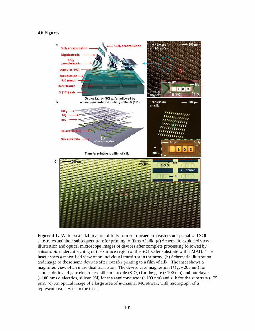
101
4.6 Figures
Figure 4-1. Wafer-scale fabrication of fully formed transient transistors on specialized SOI
substrates and their subsequent transfer printing to films of silk. (a) Schematic exploded view
illustration and optical microscope images of devices after complete processing followed by
anisotropic undercut etching of the surface region of the SOI wafer substrate with TMAH. The
inset shows a magnified view of an individual transistor in the array. (b) Schematic illustration
and image of these same devices after transfer printing to a film of silk. The inset shows a
magnified view of an individual transistor. The device uses magnesium (Mg; ~200 nm) for
source, drain and gate electrodes, silicon dioxide (SiO2) for the gate (~100 nm) and interlayer
(~100 nm) dielectrics, silicon (Si) for the semiconductor (~100 nm) and silk for the substrate (~25
µm). (c) An optical image of a large area of n-channel MOSFETs, with micrograph of a
representative device in the inset.

102
Figure 4-2. Scanning electron microscope (SEM) images showing fabrication processes of n-
channel metal-oxide semiconductor field-effect transistors (MOSFETs), (a) metallization, (b) RIE
trench etch and (c) Tetramethylammonium hydroxide (TMAH) solution etch. (d) Cross-section
view of device using scanning electron microscopy (SEM) after anisotropic TMAH etch (left)
and its magnified view (right). The thickness of entire layers is less than 2 µm.

103
Figure 4-3. Detailed fabrication process of fully biodegradable transistor array. Device isolation,
metallization, RIE trench etch, and anisotropic TMAH undercut etch (from left to right). (a)
Optical microscope images of fabrication process of n-channel transistor array. (b) Images of
scanning electron microscopy (SEM) showing n-MOSFETs fabrication process at angled view. (c)
A set of images describing fabrication of device array at tilted view. (d) Cross-sectional images of
each fabrication step of a n-channel MOSFET.
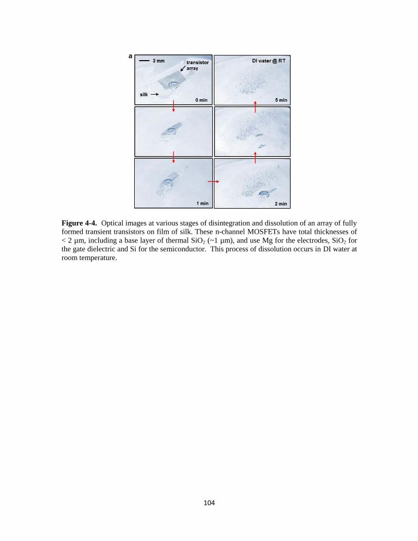
104
Figure 4-4. Optical images at various stages of disintegration and dissolution of an array of fully
formed transient transistors on film of silk. These n-channel MOSFETs have total thicknesses of
< 2 µm, including a base layer of thermal SiO2 (~1 µm), and use Mg for the electrodes, SiO2 for
the gate dielectric and Si for the semiconductor. This process of dissolution occurs in DI water at
room temperature.

105
Figure 4-5. Fabrication of arrays of transient inverters and logic gates and their electrical
properties. (a) Image of an array of inverters, optical microscope image of a representative device
(lower left) and circuit diagram (lower right). (b) SEM and optical microscope images of key
steps in the fabrication sequence. Device isolation (upper left), metallization (upper middle), RIE
trench etch (lower left), anisotropic undercut etch with TMAH (upper right, lower right), and
magnified image (lower middle). (c) Linear (red) and log scale (blue) transfer curves of an n-
channel MOSFET (channel length (Lch) and width (W) are 10 µm and 40 µm, respectively). The
mobility and on/off ratio are 650 cm2/V·s, and > 10
5, respectively. (Experimental results (lines)
and simulations (dots)) (d) I-V characteristics of an n-channel MOSFET. (e) Output voltage
characteristics and voltage gain of an inverter (Lch and W are 20 µm and 10 µm for load transistor
and 10 µm and 40 µm for input transistor, respectively). The peak gain is ~4. (f) Demonstration
of a pair of n-channel MOSFETs in a logic gate (NAND) formed by interconnection with Mg.
When one or both of the input transistors (at VA or VB) are in their off state, the associated
resistance of the input exceeds that of the load transistor, thereby leading to an output voltage in
the “1” state. When the input transistors are turned on, the output voltage reaches the “0” state.
Images after RIE trench etch (left) and after transfer and interconnection on a silk substrate (right).
Circuit diagrams appear in the top regions of the images on the left. (g) Output voltage
characteristics of logic gates (NAND) at VDD = 3 V. VA and VB represent input voltages. (h)
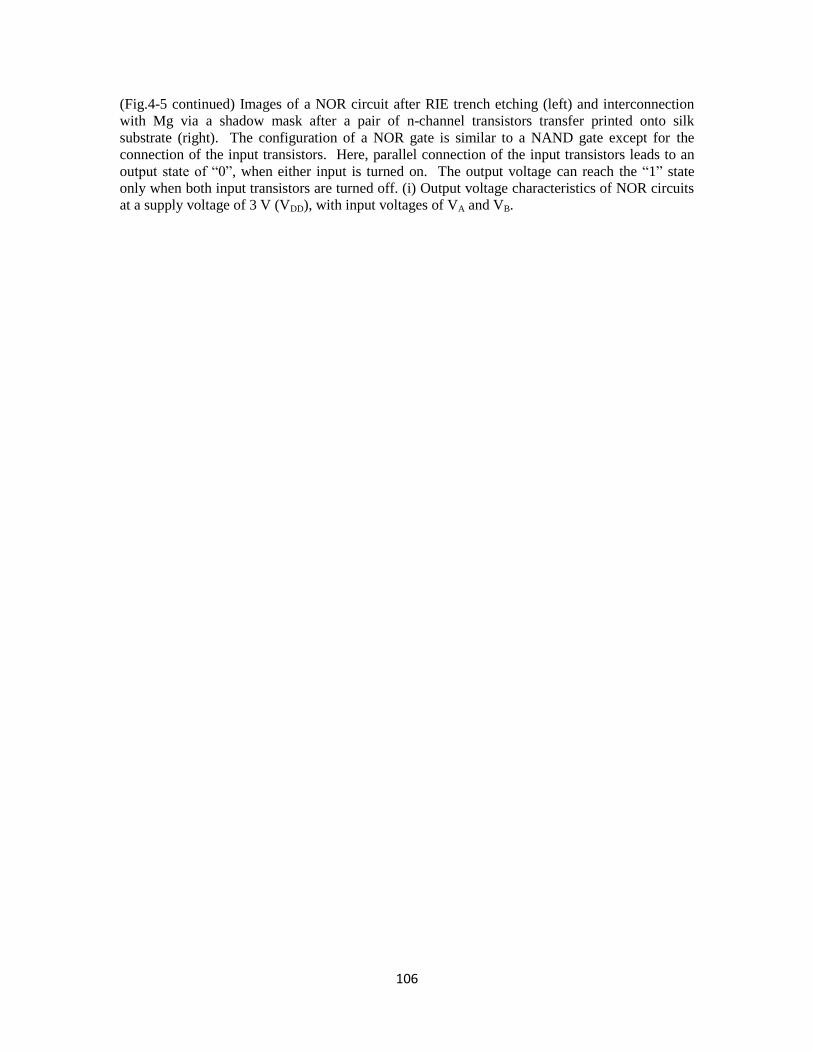
106
(Fig.4-5 continued) Images of a NOR circuit after RIE trench etching (left) and interconnection
with Mg via a shadow mask after a pair of n-channel transistors transfer printed onto silk
substrate (right). The configuration of a NOR gate is similar to a NAND gate except for the
connection of the input transistors. Here, parallel connection of the input transistors leads to an
output state of “0”, when either input is turned on. The output voltage can reach the “1” state
only when both input transistors are turned off. (i) Output voltage characteristics of NOR circuits
at a supply voltage of 3 V (VDD), with input voltages of VA and VB.
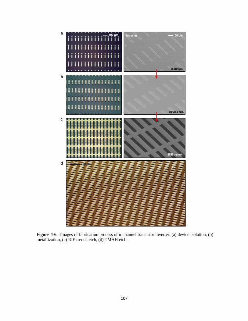
107
Figure 4-6. Images of fabrication process of n-channel transistor inverter. (a) device isolation, (b)
metallization, (c) RIE trench etch, (d) TMAH etch.

108
Figure 4-7. Optical microscope images showing fabrication process of logic gates, device
isolation, metallization, RIE trench etch and anisotropic TMAH solution etch (from top to
bottom). (a) NAND, (b) NOR.

109
Figure 4-8. Schematic illustrations and time sequence of optical micrographs during dissolution
of a transient inverter undercut etched but tethered at its ends to a Si wafer substrate. Series of
microscope images showing dissolution of an inverter device at various times of immersion in a
phosphate buffered saline (PBS) solution at physiological temperature (37 °C) and pH (~7.4).
The frames on the middle and lower left provide schematic exploded view illustrations. The
constituent materials include Si (100) with a thickness of ~100 nm for the semiconductor, Mg
(~200 nm) for the electrodes, and SiO2 (~100nm) for the gate and interlayer dielectric.
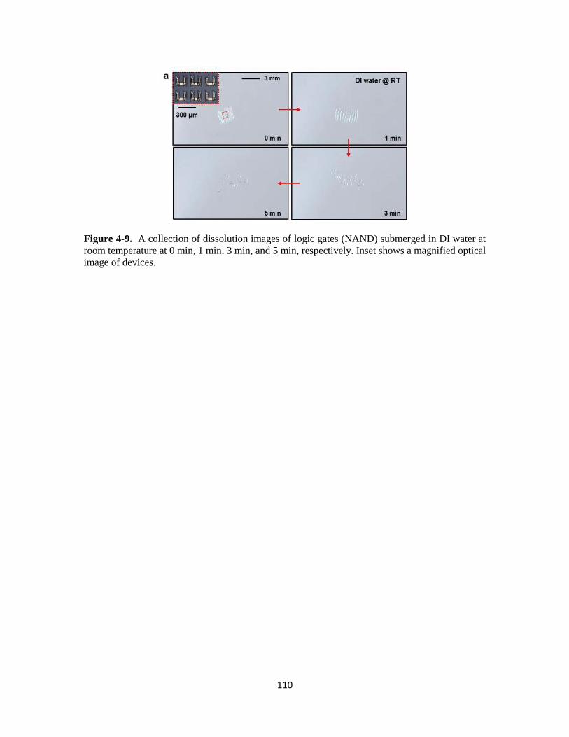
110
Figure 4-9. A collection of dissolution images of logic gates (NAND) submerged in DI water at
room temperature at 0 min, 1 min, 3 min, and 5 min, respectively. Inset shows a magnified optical
image of devices.
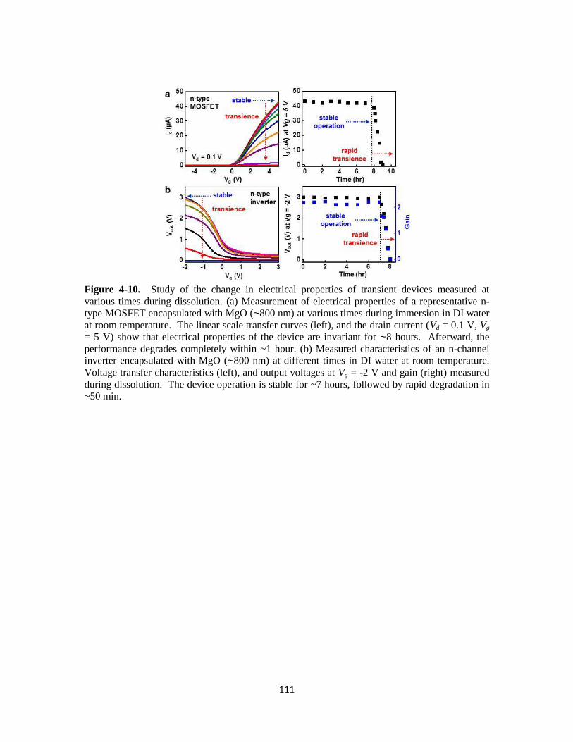
111
Figure 4-10. Study of the change in electrical properties of transient devices measured at
various times during dissolution. (a) Measurement of electrical properties of a representative n-
type MOSFET encapsulated with MgO (~800 nm) at various times during immersion in DI water
at room temperature. The linear scale transfer curves (left), and the drain current (Vd = 0.1 V, Vg
= 5 V) show that electrical properties of the device are invariant for ~8 hours. Afterward, the
performance degrades completely within ~1 hour. (b) Measured characteristics of an n-channel
inverter encapsulated with MgO (~800 nm) at different times in DI water at room temperature.
Voltage transfer characteristics (left), and output voltages at Vg = -2 V and gain (right) measured
during dissolution. The device operation is stable for ~7 hours, followed by rapid degradation in
~50 min.

112
Figure 4-11. The change of calculated mobility in n-type transistors encapsulated with MgO
(~800 nm) while submerged in DI water at room temperature.
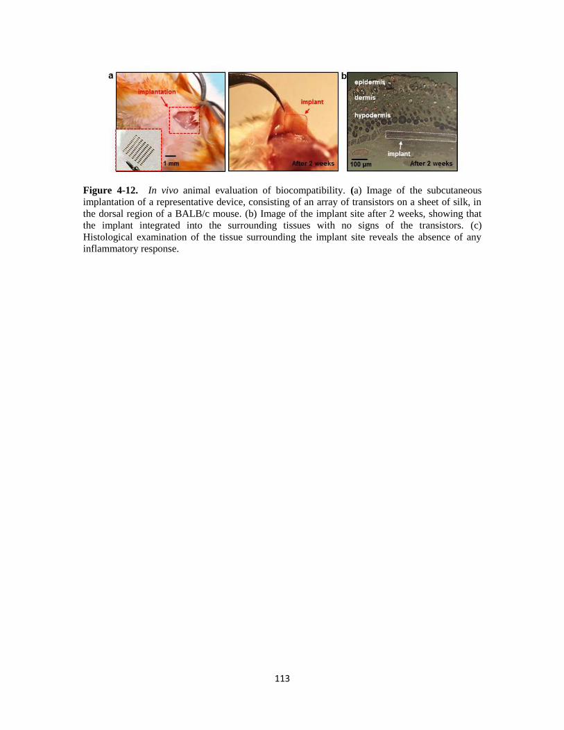
113
Figure 4-12. In vivo animal evaluation of biocompatibility. (a) Image of the subcutaneous
implantation of a representative device, consisting of an array of transistors on a sheet of silk, in
the dorsal region of a BALB/c mouse. (b) Image of the implant site after 2 weeks, showing that
the implant integrated into the surrounding tissues with no signs of the transistors. (c)
Histological examination of the tissue surrounding the implant site reveals the absence of any
inflammatory response.

114
CHAPTER 5
4TRANSIENT, BIOCOMPATIBLE ELECTRONICS BASED ON ZNO
5.1 Introduction
Semiconducting oxides are of growing interest as replacements for silicon in thin film
transistors for active matrix display backplanes; they are also of potential use in transparent,
flexible electronics and energy harvesters. Zinc oxide (ZnO), in particular, has favorable
combination properties, including excellent transparency in the visible wavelength range [1], high
electron mobility [2], and strong piezoelectric responses [3]. As a result, ZnO, in forms ranging
from films to wires and rods, has been explored in sensing [4-6], catalysis [7,8], optical emission
[9,10], piezoelectric transduction [11], and actuation [12]. Previous work also suggests that ZnO
is biocompatible [13-15], and therefore suitable for devices that integrate on or in the human body.
Here we introduce classes of ZnO based electronic devices that have, as their key attribute, the
ability to dissolve completely in water or biofluids. In this way, ZnO provides an alternative to
silicon [16] or organic semiconductors [17-20] for physically transient forms of electronics and
sensors, with expanded capabilities in energy harvesting, light emission and others. In addition to
ZnO, the other constituent materials of the devices presented here include magnesium (Mg) for
electrodes and interconnects, silicon dioxide (SiO2) or magnesium oxide (MgO) for the dielectrics,
and films of silk fibroin film for the substrate and package. Each material used here is also
biocompatible, as discussed in previous reports [21-26]. We report specific designs and
fabrication schemes for ZnO thin film transistors and mechanical energy harvesters (also for use
as strain gauges). Detailed studies reveal the kinetics of dissolution and the ability to use
4 Reprinted, by permission [DOI: 10.1002/smll.201300146] Copyright © 2013 WILEY-VCH Verlag
GmbH & Co. KGaA, Weinheim

115
materials and design choices to control this kinetics. Combined experimental/theoretical work
illustrates the key operational features of the devices.
5.2 Experiments
All electronic materials for ZnO TFTS were directly deposited onto silk through high
resolution stencil masks made of polyimide (PI) films (Kapton, 12.5 µm, Dupont, USA). These
materials consist of ZnO (semiconductor), Mg (conductors), MgO (insulators), silk (substrate). A
layer of Mg (150 nm) deposited by electron beam evaporation (Temescal) defined the source and
drain electrodes for the TFTs. ZnO (200 nm) deposited by RF magnetron sputtering (AJA)
through a PI mask served as the semiconductor. A high-purity of ZnO target was used (99.99%),
with base pressures of 2×10⁻⁶
torr, and working pressures of 15 mTorr, maintained with a Ar
(99.99 %) : O2 = 2 : 1 (sccm) gas mixture. The sputtering was performed at room temperature
(RT) with an RF power of 250 W, immediately after cleaning the target with Ar plasma for 5 min.
The deposition rate was ~150 nm/hour. Electron beam evaporation of MgO (100 nm), also
through PI masks, defined the gate dielectrics. The gate consisted of Mg (300 nm), deposited and
patterned using schemes similar to those for the source and drain.
Dissolution tests were performed to study degradation behaviors of devices and kinetics
of materials removal. To observe dissolution of ZnO, a meander trace of ZnO (200 nm) on a
glass substrate was submerged in DI water at room temperature. Optically significant changes
were observed after 9 hours, and complete disappearance occurred within 15 hours. In a similar
way, a ZnO transistor, consisting of Mg, MgO and ZnO, on glass was used to illustrate the
various stages of dissolution at the device level. Most components disappeared within 8 hours;
complete dissolution occurred within 15 hours. In addition, measurements of changes in
electrical properties defined timescales of device function. A transistor with a design similar to
that described above was prepared and then encapsulated with a layer of MgO (500 nm).
116
Measured and calculated characteristics revealed two-stage kinetics. The first was determined by
the encapsulation layer; the second, primarily by the Mg electrodes.
5.3 Results and discussion
Figure 5-1a and b provide a schematic diagram and an image of water-soluble ZnO thin
film transistors (TFTs) and mechanical energy harvesters (MEHs) / strain gauges. Sheets of silk
fibroin provide substrates and, in certain cases, encapsulating layers. Magnesium, patterned by
electron beam evaporation through fine-line stencil masks made of polyimide (PI) films (Kapton,
12.5 µm, Dupont, USA), serves as the electrodes and interconnects (thicknesses between 200 and
500 nm). A first layer of Mg defines the source/drain electrodes for the TFTs (and, therefore the
channel length, Lch) and the bottom electrodes of the MEHs. Sputter deposition of thin films of
ZnO (thicknesses between 350 and 500 nm) through PI masks forms semiconducting and
piezoelectric components of the devices. The widths of the ZnO films define the channel widths
(W) of the transistors. Layers of MgO (thicknesses between 100 and 150 nm) deposited by
electron beam evaporation through PI masks form the gate dielectric layers for the TFTs. An
additional patterned deposition of Mg (~400 nm) yields top electrodes for MEHs, and source,
drain and gate contacts for the TFTs. A top encapsulating layer of silk can be applied by spin
casting. All constituent materials, i.e. Mg (electrodes, contacts and interconnects), MgO (gate
and interlayer dielectrics), ZnO (active material for the TFTs and energy harvesters / strain
gauges) and silk (substrate and encapsulant), dissolve in water. The products of this dissolution
include Mg(OH)2, Si(OH)4 and Zn(OH)2. Previous studies suggest that these products, and the
device materials themselves, are biocompatible and environmentally benign [14,27,28]. Figure 5-
1c includes a set of images collected in a time sequence during dissolution in deionized water (DI)
at room temperature. The silk substrate (~25 µm), in the formulation used for this example,
quickly disappears by simple dissolution. This process causes the device structures to physically
117
disintegrate. Afterward, each remaining material disappears due to hydrolysis at different rates,
as described in the following sections and previous reports [29-33]. The time frames for
dissolution can be programmed not only by encapsulation and packaging methods, but also by
choices of dimensions, thicknesses and configurations in the materials for the device structures.
Dissolution of the constituent materials, other than the silk, involves hydrolysis to
produce metal hydroxides. In the case of ZnO, the product is zinc hydroxide (Zn(OH)2), as a
result of the reaction ZnO + H2O ↔ Zn(OH)2. Figure 5-2a shows a collection of images of a
meander trace of ZnO (200 nm) at various times during hydrolysis. The trace completely
disappears after 15 hours, in DI water at room temperature. The mechanisms of dissolution of
ZnO can be analytically described by reactive diffusion models, in which water diffusion into the
materials is the rate limiting process. Previous reports describe in detail the dissolution behaviors
of ZnO and the dependence on pH, temperature, dimensions and surface structures [27,34-37].
Additional experiments on dissolution, monitored by measurements of thickness as a function of
time of immersion in several different types of solutions, such as PBS, serum, and comparison of
the results with theoretical models appear in Figure 5-3a. The rate of dissolution ZnO increases
with decreasing pH, consistent with previous literature reports [27]. In acidic solution, the
dissolution of ZnO is also attributed to the reaction, ZnO + 2H+ → Zn2 + H2. A set of optical
micrographs shows a fully formed ZnO TFT undergoing dissolution under similar conditions, as
presented in Figure 5-2b. All electronic materials, i.e. Mg, MgO and ZnO, completely dissolve in
15 hours after immersion in DI water at room temperature, in a controlled manner, without
cracking, flaking or delamination. For the device dimensions studied here, the thicknesses of the
layers determine, in large part, the timescales for dissolution.
Figure 5-2c summarizes the temporal variation in the electrical properties of a ZnO TFT,
as it dissolves. (See Figure 5-3b for an image and diagram of the device.) In this case, a plate of
glass serves as the substrate, and a layer of MgO (500 nm), deposited by electron beam
evaporation, encapsulates the entire system everywhere except at the contacts for source, drain,

118
and gate electrodes which themsleves are not immersed. Measured transfer curves, drain currents
(Id) and peak transconductances show stable operation for ~3 hours, followed by rapid
degradation over the next ~45 min. (Additional electrical properties appear in Figure 5-3c.) The
encapsulant and the device materials (mainly the Mg in this case) define the first and second
timescales, respectively. The results of Figure 5-2c are only representative. The encapsulant
material and thickness can be selected to achieve stable periods of device operation that match
requirements for specific applications. For example, silk can be combined with MgO
encapsulation in a way that adjusts its crystallinity to enable the lifetime of devices to extend
from minutes to years, as demonstrated in previous results [16]. Complete electrical and
mechanical measurements on transient ZnO TFTs and MEHs appear in Figure 5-4. All electrical
measurements and bending studies were performed in a dry environment. Here, the TFTs use Mg
(150 nm, source, drain and gate electrodes), ZnO (200 nm, active layer), MgO (100 nm, gate
dielectric). Figure 5-4b illustrates additional details in optical micrographs of a typical TFT,
collected after defining the channel configuration (top) and completing the fabrication (bottom).
Analysis of current-voltage (I-V) characteristics, and linear and log scale transfer curves (Figure
5-4c and d) of a typical device (channel length (Lch) and width (W) are 20 µm and 500 µm,
respectively) yield a mobility of ~0.95 cm2/V·s, an on/off ratio of > 10
3, a sub-threshold swing of
~1 V/dec (at Vd = 0.1 V) and a threshold voltage of ~1 V. (See details on contact resistance of
Mg in Figure 5-3d). These properties are similar to those of non-transient counterparts reported
previously [38-41]. Previous literature studies suggest that deposition procedures and subsequent
processing conditions for ZnO strongly affect the electrical properties [38,42-45]. Our work
involves the constraint that the deposition and processing conditions must be compatible with silk.
Careful parametric studies reveal conditions for sputter deposition that yield transistor
characteristics (i.e. mobilities, on/off ratios, etc) in transient devices on silk that fall into a well
established range set by more conventional sets of materials and substrates [40,46].
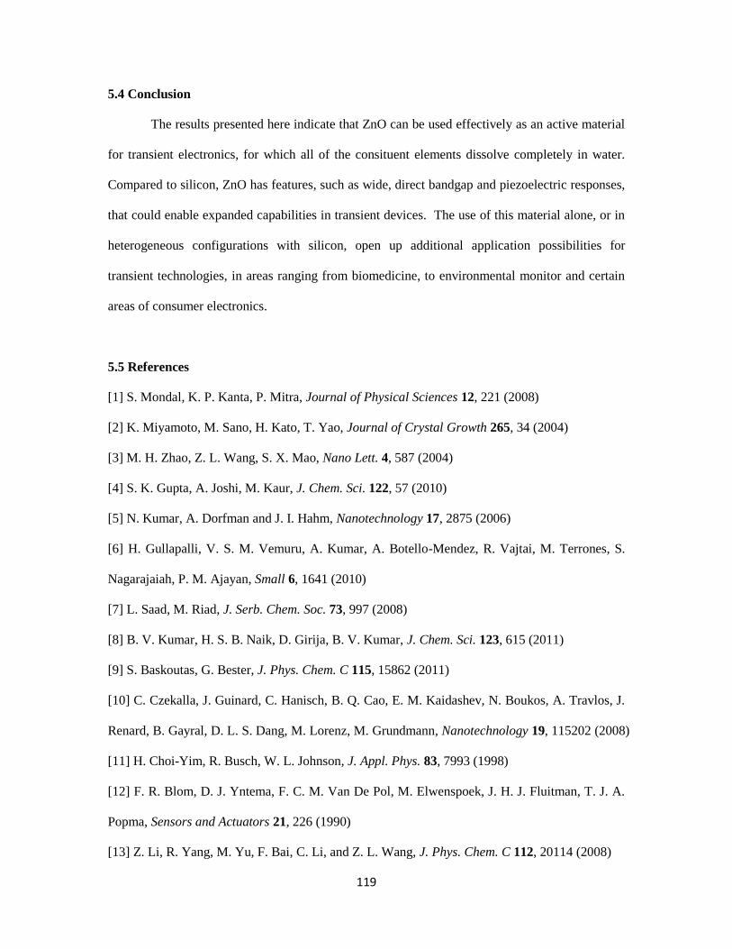
119
5.4 Conclusion
The results presented here indicate that ZnO can be used effectively as an active material
for transient electronics, for which all of the consituent elements dissolve completely in water.
Compared to silicon, ZnO has features, such as wide, direct bandgap and piezoelectric responses,
that could enable expanded capabilities in transient devices. The use of this material alone, or in
heterogeneous configurations with silicon, open up additional application possibilities for
transient technologies, in areas ranging from biomedicine, to environmental monitor and certain
areas of consumer electronics.
5.5 References
[1] S. Mondal, K. P. Kanta, P. Mitra, Journal of Physical Sciences 12, 221 (2008)
[2] K. Miyamoto, M. Sano, H. Kato, T. Yao, Journal of Crystal Growth 265, 34 (2004)
[3] M. H. Zhao, Z. L. Wang, S. X. Mao, Nano Lett. 4, 587 (2004)
[4] S. K. Gupta, A. Joshi, M. Kaur, J. Chem. Sci. 122, 57 (2010)
[5] N. Kumar, A. Dorfman and J. I. Hahm, Nanotechnology 17, 2875 (2006)
[6] H. Gullapalli, V. S. M. Vemuru, A. Kumar, A. Botello-Mendez, R. Vajtai, M. Terrones, S.
Nagarajaiah, P. M. Ajayan, Small 6, 1641 (2010)
[7] L. Saad, M. Riad, J. Serb. Chem. Soc. 73, 997 (2008)
[8] B. V. Kumar, H. S. B. Naik, D. Girija, B. V. Kumar, J. Chem. Sci. 123, 615 (2011)
[9] S. Baskoutas, G. Bester, J. Phys. Chem. C 115, 15862 (2011)
[10] C. Czekalla, J. Guinard, C. Hanisch, B. Q. Cao, E. M. Kaidashev, N. Boukos, A. Travlos, J.
Renard, B. Gayral, D. L. S. Dang, M. Lorenz, M. Grundmann, Nanotechnology 19, 115202 (2008)
[11] H. Choi-Yim, R. Busch, W. L. Johnson, J. Appl. Phys. 83, 7993 (1998)
[12] F. R. Blom, D. J. Yntema, F. C. M. Van De Pol, M. Elwenspoek, J. H. J. Fluitman, T. J. A.
Popma, Sensors and Actuators 21, 226 (1990)
[13] Z. Li, R. Yang, M. Yu, F. Bai, C. Li, and Z. L. Wang, J. Phys. Chem. C 112, 20114 (2008)

120
[14] Y. F. Zheng, R. Z. Li, Y. D. Wang, International Journal of Modern Physics B 23, 1566
(2009)
[15] S. Dutta, S. Basak, P. K. Samanta, International Journal of NanoScience and
Nanotechnology 3, 27 (2012)
[16] S. W. Hwang, H. Tao, D. H. Kim, H. Cheng, J. K. Song, E. Rill, M. A. Brenckle, B.
Panilaitis, S. M. Won, Y. S. Kim, Y. M. Song, K. J. Yu, A. Ameen, R. Li, Y. Su, M. Yang, D. L.
Kaplan, M. R. Zakin, M. J. Slepian, Y. Huang, F. G. Omenetto, J. A. Rogers, Science 337, 1640
(2012)
[17] C. Legnani, C. Vilani, V. L. Calil, H. S. Barud, W. G. Quirino, C.A. Achete, S. J. L. Ribeiro,
M. Cremona, Thin Solid Films 517, 1016 (2008)
[18] M. Irimia-Vladu, P. A. Troshi, M. Reisinger, L. Shmygleva, Y. Kanbur, G. Schwabegger, M.
Bodea, R. Schwödiauer, A. Mumyatov, J. W. Fergus, V. F. Razumov, H. Sitter, N. S. Sariciftci, S.
Bauer, Adv. Funct. Mater. 20, 4069 (2010)
[19] C. J. Bettinger, Z. Bao, Polym Int. 59, 563 (2010)
[20] C. J. Bettinger, Z. Bao, Adv. Mater. 22, 651 (2010)
[21] B. Panilaitis, G. H. Altman, J. Chen, H. J. Jin, V. Karageorgiou, D. L. Kaplan, Biomaterials
24, 3079 (2003)
[22] M. Moravej, D. Mantovani, Int. J. Mol. Sci. 12, 4250 (2011)
[23] S. P. Hudson, R. F. Padera, R. Langer, D. S. Kohane, Biomaterials 29, 4045 (2008)
[24] B. G. Trewyn, J. A. Nieweg, Y. Zhao, V. S. Y. Lin, Chemical Engineering Journal 137, 23
(2008)
[25] S. Shen ,P. S. Chow ,F. Chen ,R. B. Tan, Chem. Pharm. Bull. 55, 985 (2007)
[26] C. Martinez-Boubeta, L. Balcells, R. Cristòfol, C. Sanfeliu, E. Rodríguez, R. Weissleder, S.
Lope-Piedrafita, K. Simeonidis, M. Angelakeris, F. Sandiumenge, A. Calleja, L. Casas, C.
Monty, B. Martínez, Nanomedicine : nanotechnology, biology, and medicine 6, 362 (2010)
[27] J. Zhou, N. Xu, Z. L. Wang, Adv. Mater. 18, 2432 (2006)

121
[28] I. Shimizu, D. MacFarlane, Dermatologic Surgery 38, 965 (2012)
[29] M. H. Grosjean, L. Roué, Journal of Alloys and Compounds 416, 296 (2006)
[30] D. J. Wales, J. P. K. Doye, J. Chem. Phys. 119, 12409 (2003)
[31] K.Wegnera, H. C. Lya, R. J.Weissa, S. E. Pratsinisa, A. Steinfelda, International Journal of
Hydrogen Energy 31, 55 (2006)
[32] R.B. Reed, D. A. Ladner, C.P. Higgings, P. Westerhoff, J. F. Ranville, Environ. Toxicol.
Chem. 31, 93 (2012)
[33] G.Song, A. Atrens, Advanced Engineering Materials 5, 837 (2003)
[34] M. Valtiner, S. Borodin, G.Grundmeier, Langmuir 24, 5350 (2008)
[35] C. David, J. Galceran, C. Rey-Castro, J. Puy, E. Companys, J. Salvador, J. Monne, R.
Wallace, A. Vakourov, J. Phys. Chem. 116, 11758 (2012)
[36] H. Gerischer, N. Sorg, Electrochimica Acta 37, 827 (1992)
[37] A. Mudunkotuwa, T. Rupasinghe, C. Wu, V. Grassian, Langmuir 28, 396 (2012)
[38] H. Jeon, K. Noh, D. Kim, M. Jeon, Journal of the Korean Physical Society 51, 1999 (2007)
[39] X. Zhang, J. Zhang, W. Zhang, X. Hou, J Mater Sci: Mater Electron 21, 671 (2010)
[40] R. Hoffman, B. Norris, J. Wagera, Appl. Phys. Lett. 82, 733 (2003)
[41] P. F. Carcia, R. S. McLean, M. H. Reilly, Appl. Phys. Lett. 88, 123509 (2006)
[42] C. Chang, V. H. Tran, J. Wang, Y. K. Fuh, L. Lin, Nano Lett. 10, 726 (2010)
[43] G. B. Stringfellow, Organometallic Vapor-Phase Epitaxy: Theory and Practice, Academic,
San Diego p. 4 (1998)
[44] S. Masuda, K. Kitamura, Y. Okumura, S. Miyatake, H. Tabata, T. Kawai, J. Appl. Phys. 93,
1624 (2003)
[45] J. M. Camacho, R. Castro-Rodríguez, A. Iribarren, E. Chan y Díaz, A. Duarte-Moller, P.
Sánchez Santiago, International Journal of the Physical Sciences 6, 6660 (2011)
[46] C. J. Park, Y. W. Kim, Y. J. Cho, S. M. Bobade, D. K. Choi, S. B. Lee, Journal of the
Korean Physical Society 55, 1925 (2009)

122
5.6 Figures
Figure 5-1. Materials and designs for transient thin film transistors (TFTs) and mechanical
energy harvesters (MEHs) / strain gauges based on ZnO, Mg, MgO and silk. (a) Schematic
illustration of transient ZnO TFTs and MEHs / strain gauges that consist entirely of water soluble
materials: ZnO (semiconductor / piezoelectric), Mg (conductor), MgO (insulator), silk (substrate).
(b) Photograph of a collection of ZnO TFTs and MEHs on a silk substrate. All electronic
materials were deposited through high resolution shadow masks made of polyimide (PI) film
(Kapton, 12.5µm, Dupont, USA). (c) A set of images of an array of ZnO TFTs and MEHs on silk,
at various times after immersion in deionized water at room temperature.

123
Figure 5-2. Dissolution kinetics of water soluble electronic materials, and devices. (a) A series
of optical microscope images collected at various times during dissolution of a meander trace of
ZnO (200 nm) immersed in deionized water at room temperature. (b) Images of a representative
ZnO TFT at various times during dissolution. All components fully dissolve. (c) Experimental
results of degradation in electrical properties of a ZnO TFT encapsulated with MgO (500 nm) at
various times after immersion in water. The linear scale transfer curves (left) and the drain
current (Id) at drain and gate voltages of Vd = 0.1 V and Vg = 5 V, respectively, and the peak
transconductance (left) show that the operation of the device is stable for ~3 hours, after which
the properties quickly degrade in ~45 min.

124
Figure 5-3. (a) Experimental (E) and theoretical (T) changes in the thickness of a thin film of
ZnO as a function of time, during dissolution in different solutions: phosphate buffer solution
(PBS, pH 4, blue), DI water (pH 7.5, black), bovine serum (pH 8.7, red). (b) Image of the ZnO
TFT used to study dissolution kinetics at the device level, with a circuit diagram. (c) Calculated
mobility (red) and on/off ratio (blue), corresponding to transfer curves in the right frame of Figure
5-2c. (d) Width-normalized on-state resistance at various channel lengths and gate biases.
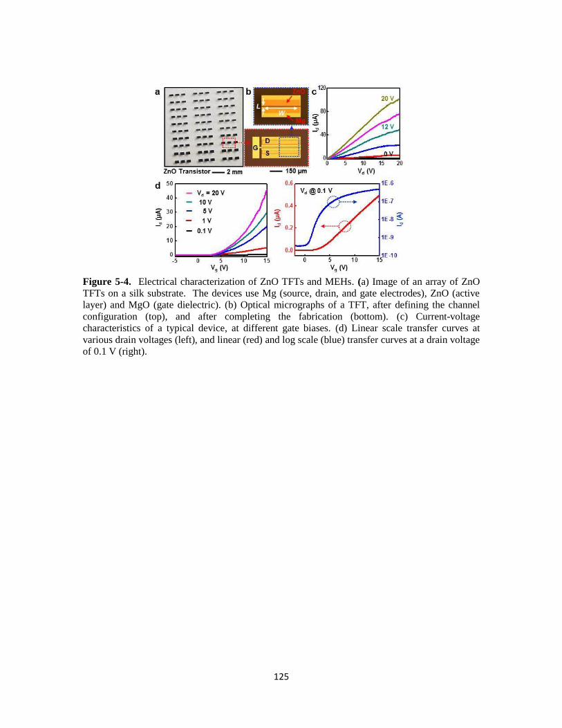
125
Figure 5-4. Electrical characterization of ZnO TFTs and MEHs. (a) Image of an array of ZnO
TFTs on a silk substrate. The devices use Mg (source, drain, and gate electrodes), ZnO (active
layer) and MgO (gate dielectric). (b) Optical micrographs of a TFT, after defining the channel
configuration (top), and after completing the fabrication (bottom). (c) Current-voltage
characteristics of a typical device, at different gate biases. (d) Linear scale transfer curves at
various drain voltages (left), and linear (red) and log scale (blue) transfer curves at a drain voltage
of 0.1 V (right).
126
CHAPTER 6
DEVICE DESIGN AND MANUFACTURING APPROACH FOR TRANSIENT
ELECTRONIC SYSTEM INTEGRATED ONTO BIODEGRADABLE AND
BIOCOMPATIBLE POLYMER SUBSTRATE
6.1 Introduction
Biodegradable polymers are of growing interest as their implantable biomedical
applications, such as bioresorbable surgical devices, a drug delivery carrier and scaffolds for
tissue engineering [1-8]. The poly lactic-co-glycolic acid (PLGA), a copolymer of poly lactic
acid (PLA) and poly glycolic acid (PGA), is the most popular among the various biodegradable
polymers since its properties can be tuned by adjusting molecular weight and ratio of lactide to
glycolide. In water, PLGA is experienced degradation by hydrolysis of its ester linkages, and
lactide rich PLGA is more hydrophobic and absorb less water, therefore degradation rate is
slower. Past approach for constructing electronic systems on PLGA substrates was explored by
organic active materials. This partially resorbable system, however, needs a temperature control
system during deposition of metals for electrodes and semiconductors due to lower glass
transition temperature (Tg) of PLGA. Using shadow masks for deposition process can limit
device shapes and/or sizes, and solution casting procedures are required to perform a dehydration
process at the end. Here we propose the fabrication schemes that enable to transfer the whole
device circuits printing onto PLGA substrate, which can probably remove all limitations existing
in organic electronic devices with restorable biomaterials in previous studies [9-10]. The result is
very important to a route to high performance silicon complementary metal-oxide-
semiconductor (CMOS) systems that enable to integrate on diverse biodegradable polymers,
which cannot be addressed in previous approaches due to intrinsic properties of resorbable
biomaterials.
127
6.2 Experiments
Three different doping procedures were performed on an n-type SOI wafer (SOITEC,
France) for fabrication of transient silicon cmos inverters. Boron doping at 550 °C using spin-on
dopant (SOD, Filmtronics, USA) defined lightly doped regions for the p-wells (p-). Heavily
doped p-type regions for source and drain electrodes were formed at 1050 °C for p-type
transistors. Phosphorous doping at 950 °C defined highly doped areas for source and drain
contacts for n-type transistors. Removal of the box oxide by wet etching with HF released the top
device silicon from the SOI, and transfer printed onto a spin cast film of PMMA/D-PI on silicon
carrier substrate. Doped silicon nanomembrane (Si NM) was isolated by reactive ion etching
(RIE; Plasmatherm) with sulfur hexafluoride (SF6) gas. A very thin layer of PE-CVD SiO2 (~50
nm) was used as gate dielectric, followed by etching contact pads by buffered oxide etchant for
source and drain electrodes. A 300 nm of Mg electrodes for the source, drain, gate contacts, and
interconnects were deposited by ebeam evaporator, followed by another thin layer of D-PI. In
order to undercut the underlying sacrificial layer of PMMA to release an ultrathin circuit from the
temporal carrier substrate, mesh structure was defined to remove certain regions of polymer
layers (D-PI, PMMA) and SiO2 layer. Immersion in acetone washes away the PMMA layer, and
the freestanding device can be retracted by PDMS. Next, the bottom layer of D-PI was removed
by oxygen (O2) gas (March RIE), and the circuit was transfer printed onto biodegradable
polymers. Finally, the top layer of D-PI was removed by RIE.
6.3 Results and discussion
Figure 6-1a describes the key procedures for manufacturing strategy of transient
electronic devices that can be integrated onto bioresorbable polymer materials, which can be
applied to nearly any kind of substrate, including poly lactic-co-glycolic acid (PLGA),
polycaprolactone (PCL), polylactic acid (PLA), cellulose and rice paper. The procedure begins

128
with spin casting a sacrificial layer of poly (methylmethacrylate) (PMMA) followed by an
ultrathin substrate layer of diluted polyimide (D-PI) (~200 nm) on a temporal silicon (Si) wafer.
Doped silicon nanomembranes (SiNMs) for complementary metal–oxide–semiconductor (CMOS)
array separately formed from n-type SOI wafer were transfer printed on top of D-PI surface.
Active device region of SiNMs was defined by reactive ion etching (RIE). Depositing and
patterning plasma-enhanced chemical vapor deposition (PECVD) SiO2 (~50 nm) for gate
dielectric, and Mg (200 nm) for source, drain, gate contacts, and interconnects form transient Si-
CMOS circuits. Another layer of D-PI cast on top of the circuit. In order to undercut the
underlying sacrificial layer of PMMA to release an ultrathin circuit from the temporal carrier
substrate, mesh structure was defined to remove certain regions of polymer layers (D-PI, PMMA)
and SiO2 layer. Immersion in acetone washes away the PMMA layer, and the freestanding device
can be retracted by PDMS. Next, the bottom layer of D-PI was removed by oxygen (O2) gas
(March RIE), and the circuit was transfer printed onto biodegradable polymers. Finally, the top
layer of D-PI was removed by RIE, using same method as above. The left frame of Figure 2b
presents image of Si CMOS array on a PLGA cast paper using manufacturing method suggested,
and its magnified image in the right frame, with microscope image in the inset. Measurements on
a representative CMOS inverter appear in Figure 1c; the gain and threshold voltage (Vth) are ~50
and -1 V with Vdd = 10 V, respectively. The electrical performance of Si CMOS device
fabricated by this approach does not indicate any degradations or lower performance (Figure 3c),
which is comparable with those of previously reported devices [11].
Figure 6-2 illustrates the chemical structure of bioresorbable polymers. These materials
have been used for sutures, drug delivery vehicles, and scaffolds for tissue engineering, since they
are degraded in body via hydrolysis or enzymatically to produce biocompatible, non-toxic/safe
by-products, which are metabolized in the end [12-13]. Among various processing methods, we
used a very thin, spin cast film of polymers onto temporary carrier substrates that enable us to
adjust the thickness of substrates, which can tune/program the life span of electronic devices.

129
Biopolymers can be utilized as a freestanding form of thin sheet, but also they have
capability to be integrated on various forms of substrates, ranging from a sheet of paper to gloves,
and rice paper, due to their excellent mechanical property and intrinsic tackiness. Figure 6-3a
presents a photograph of CMOS inverter array on a thin film of PLGA substrate (10 ~ 15µm
thick), wrapped on a glass rod, including a magnified image in the inset. In addition to spin-
casting procedure to create polymer substrate, melt-process at elevated temperature is also
available for resorbable polymers. Figure 6-3b and 6-3c show images of transfer printed CMOS
inverter circuit on PCL (~1 mm thick) and PLA (~2 mm thick) substrate, respectively. Since both
polymers can provide sufficient tackiness beyond melting points, its property can overcome
adhesion strength between PDMS and the top D-PI layer, i.e. to release the system from PDMS
during transfer printing process. We note that the bonding force between PDMS and the device
surface became stronger after experiencing the oxygen RIE process. There might be opportunity
for theses biodegradable electronics to apply edible devices. Figure 6-3d illustrates bioresorbable
CMOS circuit can be integrated onto rice paper, after applying certain amount of water to the
surface of rice paper that becomes sticky enough to transfer print onto that surface. Additional
images appear in Figure 6-4. Undergoing these procedures does not limit device performances.
Figure 6-3e represents the measured electrical characteristics of a typical CMOS inverter (left)
and individual p- (middle) and n-channel (right) metal-oxide-semiconductor field-effect
transistors (MOSFETs). The gain and threshold voltage (Vth) are ~50 and -1 V, respectively.
The negative threshold voltage of the inverters arises probably from the high negative threshold
voltage (~5 V) of the p-type MOSFETs. The mobilities are ~70 cm2/V·s and ~400 cm
2/V·s, for
the p- and n-channel devices, respectively. The on/off current ratios (Ion/Ioff) are ~105 for both
cases of transistors.
In some cases, the potential applications of transient/bioresorbable electronics can be
extended to security system, green/environmentally friendly electronics and disposal process of
waste beyond biomedical implantable devices. Figure 6-5 illustrates representative case of use in
130
various fields for transient electronic system, including self-destructing device as appeared in
Figure 6-5a. Information that has been achieved by monitoring/navigating enemy base can be
delivered via wireless transfer, however, when this type of medium is unexpectedly disclosed to
hostile forces, the transient system can be destroyed by purpose or itself, which aims to secure
information collected. Modern electronic products that we typically rely on are not particularly
good to the environment, and millions of devices made of materials posing any types of threat to
surroundings are increasingly consumed and disposed day by day. There might be some
possibilities for us to avoid harmful/toxic materials utilized in certain type of electronic devices,
i.e. use of transient materials for the purpose of manufacturing eco-safe devices, with comparable
electrical performance over the conventional electronic devices, as illustrated in Figure 6-5b and
6-5c. Another possibility is lying on managing huge amount of incoming waste stream. Figure
6-5d describes a concept of biodegradable/compostable electronic devices that completely
disappear/vanish over time after useful time periods in function, which enable to cut down cost
and hazard for disposal process avoid recovery and collection after use.
6.4 Conclusion
The concepts introduced here provide materials, manufacturing strategy and design
layouts for transient electronic circuits that can be integrated onto bioresorbable polymer
substrates. The combined use of transient devices, comprised of inorganic materials, with
biopolymers demonstrates the versatility of potentially desired applications for transient
electronic system. In particular, manufacturing scheme allows us to construct transient circuits on
nearly any type of structures and substrates.
6.5 References
[1] X. S. Wu, N. Wang, J. Biomater. Sci. Polymer Edn, 2001, 12, 21–34
[2] J. M. Anderson, M. S. Shive, Advanced Drug Delivery Reviews, 28 (1997) 5–24
131
[3] T. Ponnusamy, L. B. Lawson, L. C. Freytag, D. A. Blake, R. S. Ayyala, V. T. John, Biomatter
2:2, 77–86; April/May/June 2012;
[4] H. K. Makadia, S. J. Siegel, Polymers 2011, 3, 1377-1397
[5] K. Leja, G. Lewandowicz, Polish J. of Environ. Stud. 2010, . 19, No. 2 (2010), 255-266
[6] D. Garlotta, Journal of Polymers and the Environment, Vol. 9, No. 2, April 2001 (q 2002)
[7] M. I. Sabir, X. Xu, L. Li, J Mater Sci (2009) 44:5713–5724
[8] B. D. Ulery, L. S. Nair, C. T. Laurencin, J. Polym. Sci. B Polym. Phys. 2011 June 15; 49(12):
832–864
[9] C. X. F. Lam, M. M. Savalani, S. –H. Teoh, D. W. Hutmacher, Biomed. Mater. 3 (2008)
034108 (15pp)
[9] C. J. Bettinger, Z. Bao, Adv. Mater. 2010, 22, 651.
[10] M. Irimia-Vladu, P. A. Troshin, M. Reisinger , L. Shmygleva, Y. Kanbur , G. Schwabegger,
M. Bodea, R. Schwödiauer, A. Mumyatov, J. W. Fergus , V. F. Razumov, Helmut Sitter, N. S.
Sariciftci, S. Bauer, Adv. Funct. Mater. 2010, 20, 4069.
[11] S.-W. Hwang et al., Adv. Mater. DOI: 10.1002/adma.201300920
[12] M. A. Woodruff, D. W. Hutmacher, Prog Polym Sci (2010),
doi:10.1016/j.progpolymsci.2010.04.002
[13] D. W. Hutmacher, J. Biomater. Sci. Polym. Ed. 12, 107 (2001).
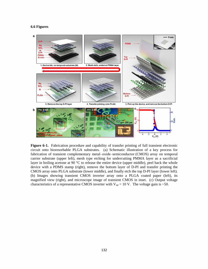
132
6.6 Figures
Figure 6-1. Fabrication procedure and capability of transfer printing of full transient electronic
circuit onto bioresorbable PLGA substrates. (a) Schematic illustration of a key process for
fabrication of transient complementary metal–oxide–semiconductor (CMOS) array on temporal
carrier substrate (upper left), mesh type etching for undercutting PMMA layer as a sacrificial
layer in boiling acetone at 90 °C to release the entire device (upper middle), peel back the whole
device with a PDMS stamp (right), remove the bottom layer of D-PI and transfer printing the
CMOS array onto PLGA substrate (lower middle), and finally etch the top D-PI layer (lower left).
(b) Images showing transient CMOS inverter array onto a PLGA coated paper (left), its
magnified view (right), and microscope image of transient CMOS in inset. (c) Output voltage
characteristics of a representative CMOS inverter with Vdd = 10 V. The voltage gain is ~50.
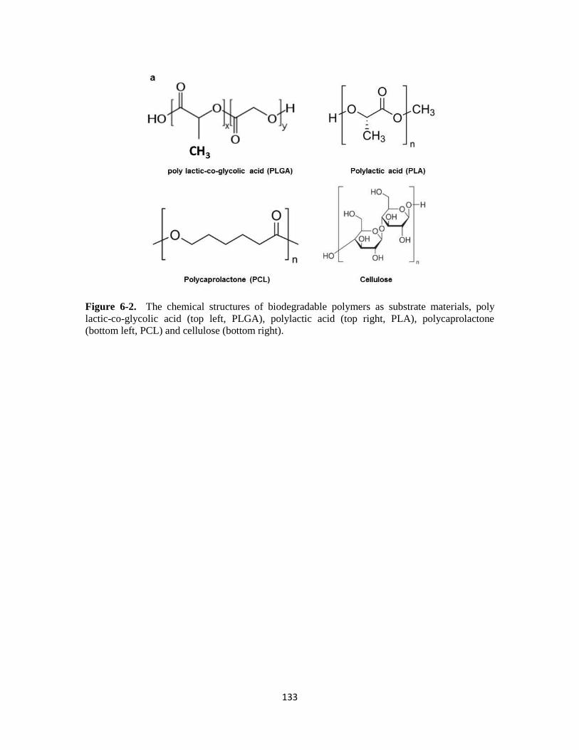
133
Figure 6-2. The chemical structures of biodegradable polymers as substrate materials, poly
lactic-co-glycolic acid (top left, PLGA), polylactic acid (top right, PLA), polycaprolactone
(bottom left, PCL) and cellulose (bottom right).

134
Figure 6-3. Transient electronic system on various biodegradable polymers, and rice paper. (a)
A photograph of CMOS inverter array on thin PLGA substrate wrapped on a cylindrical shape of
glass rod, with a magnified image in the inset. (b) Bending image of a transient device transfer
printed on resorbable PCL substrate. (c) Transient CMOS inverter array on PLA substrate. (d)
Image illustrating transient circuit transfer printed onto rice paper, after applying a little amount
of water to rice paper to obtain sufficient adhesion property. (e) Output voltage property of a
representative CMOS inverter at Vdd = 10 V, and the gain is ~80 (left). Linear (red) and log scale
(blue) transfer curves of a typical transient p-channel MOSFET. The channel length (L) and
width (W) are 5 µm and 300 µm, respectively. The mobility and on/off ratio are ~70 cm2/V·s and
~105, respectively (middle). I-V characteristics of a typical n-channel MOSFET. The channel
length (L) and width (W) are 15 µm and 100 µm, respectively. The mobility and on/off ratio are
400 cm2/V·s and ~10
5, respectively.
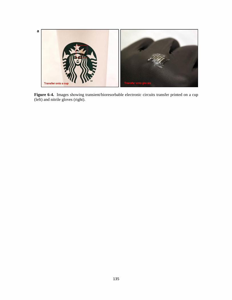
135
Figure 6-4. Images showing transient/bioresorbable electronic circuits transfer printed on a cup
(left) and nitrile gloves (right).
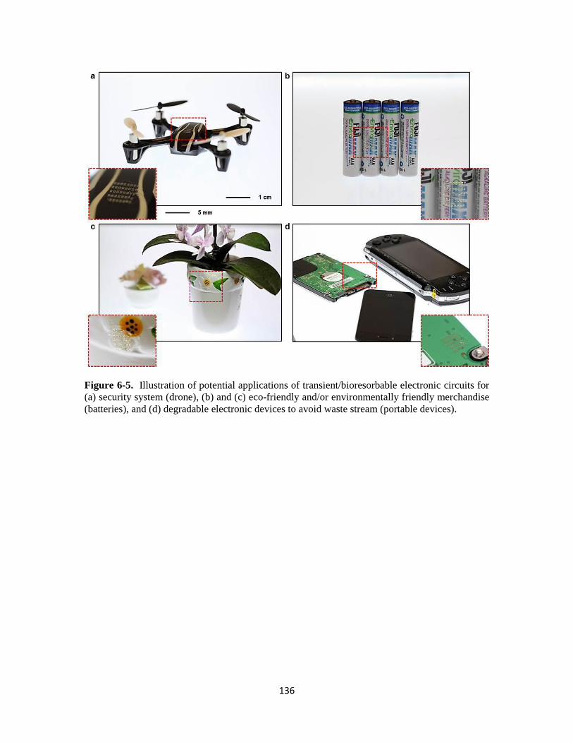
136
Figure 6-5. Illustration of potential applications of transient/bioresorbable electronic circuits for
(a) security system (drone), (b) and (c) eco-friendly and/or environmentally friendly merchandise
(batteries), and (d) degradable electronic devices to avoid waste stream (portable devices).

137
CHAPTER 7
SUMMARY AND PERSPECTIVE
Recent accomplishment establishes a new class of silicon-based electronics that can, in a
controlled manner, completely vanish over time when exposed to water or biofluids. Devices that
are ‘transient’ create application possibilities that cannot be addressed with conventional
electronics, such as active implants that exist for medically useful timeframes, but then
completely dissolve and disappear via resorption by the body. We demonstrated a comprehensive
set of materials, components, theoretical design tools and manufacturing approaches for a
complementary metal oxide semiconductor (CMOS) electronics, with integrated sensors,
actuators, power supply systems and wireless control strategies. A transient silicon electronic
device capable of delivering thermal therapy in an implantable device to address challenges in
surgical site infections caused by antibiotic-resistant bacteria and its demonstration in animal
models illustrate a system-level example of this technology. Another accomplishment is device
design and fabrication approaches to RF power scavenging and oscillator circuits that are
physically transient, in the sense that they dissolve at controlled rates when exposed to water in
the environment or the body. These physically transient circuits consist of rectifying diodes,
transistors, antennas, capacitors, inductors, and resistors, and are composed entirely of
biocompatible and environmentally friendly constituent materials.
The devices designed in the regime described above involve process steps are formed are
formed in a non-automated manner, with critical dimensions and other key characteristics that are
far below of state-of-the-art industrial business in silicon microelectronics. We recently
established manufacturing strategy that has the ability to form transient integrated circuits using
modest modifications of existing foundry fabrication processes and materials. In particular, high
quality components and systems with excellent electrical performace can be constructed using

138
tungsten as a transient metallization, for the vias as well as for the interconnects. A
manufacturable method for exploiting such transient CMOS on transient substrates does not,
however, exist yet. In addition, strategies for fabricating high performance sensors using related
methods must be developed. With this type of methods, we seek to address these gaps in
capabilities by achieving manufacturable approaches to sensors, and associated power and
transmission circuits, relevant for battlefield monitoring, and their integration into functional
wireless systems, which enable us to use for implantable biomedical applications.
The proposed direction for trasnsient electronics includes (1) combined use of novel SOI
substrates for transient CMOS and advanced techniques for transfer printing can yield a
generalized manufacturing approach, (2) designs can be developed for RF harvesting and
transmission systems, and (3) strategies are available for integrating all of these approaches into
system-level of transient wireless systems for environmental monitoring as well as implantable
biomedical devices.