matsushita electric industrial co., ltd, …...matsushita electric industrial co., ltd, nov. 14,...
TRANSCRIPT

3/3/10 2:57 AMUntitled Document
Page 1 of 51file:///Users/sethchase/Desktop/Markman/htmlfiles/2007.11.14_SAMSUNG_ELECTRONICS_CO_LTD_v._MATSUSHITA_ELECTRIC_INDUSTRIAL_CO.html
United States District Court,E.D. Texas, Tyler Division.
SAMSUNG ELECTRONICS CO., LTD,Plaintiff.v.MATSUSHITA ELECTRIC INDUSTRIAL CO., LTD,Defendant.
No. 6:06CV 154
Nov. 14, 2007.
Michael Edwin Jones, Diane DeVasto, Earl Glenn Thames, Jr., Potter Minton PC, Tyler, TX, Chong S.Park, Edward C. Donovan, F. Christopher Mizzo, Gregory F. Corbett, Laura M. Denton, Sean C.Abouchedid, Sosun Bae, Kirkland & Ellis LLP, Washington, DC, Gregory S. Arovas, Todd M. Friedman,Kirkland & Ellis, New York, NY, John Robert Robertson, Michael P. Bregenzer, Nyika O. Strickland,William E. Devitt, Kirkland & Ellis LLP, Chicago, IL, for Plaintiff.
J. Thad Heartfield, Michael Dru Montgomery, The Heartfield Law Firm, Beaumont, TX, Bijal V. Vakil,James E. Glore, Shamita D. Etienne-Cummings, McDermott, Will & Emery, Palo Alto, CA, David M.Tennant, Jack Q. Lever, Jr., Qian Huang, McDermott, Will & Emery, Washington, DC, Jennifer L.Yokoyama, McDermott, Will & Emergy, Irvine, CA, Minn Chung, Morrison & Foerster LLP, SanFrancisco, CA, Robert A. Weiner, Taina Rodriguez, McDermott, Will & Emery, New York, NY, forDefendant.
MEMORANDUM OPINION
LEONARD DAVIS, District Judge.
This Claim Construction Opinion construes terms in Samsung's asserted patents: U.S. Patent Nos. 5,091,339("the '339 patent") and 5,173,442 ("the '442 patent") (collectively, "the Carey patents") and RE 36,490 ("the '490 patent"). This Opinion also construes terms in Matshusita Electronic Industrial's ("MEI") assertedpatents: U.S. Reissue Patent Nos. 35,921 ("the '921 patent") and 35,680 ("the '680 patent") and U.S. PatentNos. 5,189,588 ("the '588 patent") and 6,677,195 ("the '195 patent").
BACKGROUND
The Samsung patents relate generally to semiconductors. the '442 patent is a continuation of a continuation-in-part of the '339 patent. The Carey patents describe a process for forming electrical wiring in multilayerinterconnect structures such as modern integrated circuits. In this process-known generally as a "dualdamascene"-channels and vias are formed and then filled with metal to form the wiring. Samsung's '490patent describes a power and signal line bussing method for memory devices located on semiconductor

3/3/10 2:57 AMUntitled Document
Page 2 of 51file:///Users/sethchase/Desktop/Markman/htmlfiles/2007.11.14_SAMSUNG_ELECTRONICS_CO_LTD_v._MATSUSHITA_ELECTRIC_INDUSTRIAL_CO.html
chips. The described power, ground, and signal wiring arrangement is designed to protect the electricalcircuitry from interference and decrease overall chip size.
The MEI's '921 and '680 patents relate generally to synchronous random access memory ("SDRAM"). Bothpatents describe using a clock signal to increase overall operational speed. The '921 patent claims aSDRAM, and the '680 patent claims a system incorporating the SDRAM claimed in the '921 patent.
MEI's '588 and '195 patents relate generally to semiconductor chip design. The '588 patent relates to anelectro-static discharge protection device and claims a surge protection apparatus utilizing multipletransistors to discharge or drain excess static. MEI's '195 patent claims a semiconductor integrated circuitdevice and method of producing such a circuit. The '195 patent discloses a semiconductor fuse structure thatallows defective areas of a chip to be disabled by disconnecting selected fuses, thereby increasing chipmanufacture production yields.
APPLICABLE LAW
"It is a 'bedrock principle' of patent law that 'the claims of a patent define the invention to which thepatentee is entitled the right to exclude.' " Phillips v. AWH Corp., 415 F.3d 1303, 1312 (Fed.Cir.2005) (enbanc) (quoting Innova/Pure Water Inc. v. Safari Water Filtration Sys., Inc., 381 F.3d 1111, 1115(Fed.Cir.2004)). In claim construction, courts examine the patent's intrinsic evidence to define the patentedinvention's scope. See id.; C.R. Bard, Inc. v. U.S. Surgical Corp., 388 F.3d 858, 861 (Fed.Cir.2004); BellAtl. Network Servs., Inc. v. Covad Commc'ns Group, Inc., 262 F.3d 1258, 1267 (Fed.Cir.2001). Thisintrinsic evidence includes the claims themselves, the specification, and the prosecution history. See Phillips,415 F.3d at 1314; C.R. Bard, Inc., 388 F.3d at 861. Courts give claim terms their ordinary and accustomedmeaning as understood by one of ordinary skill in the art at the time of the invention in the context of theentire patent. Phillips, 415 F.3d at 1312-13; Alloc, Inc. v. Int'l Trade Comm'n, 342 F.3d 1361, 1368(Fed.Cir.2003).
The claims themselves provide substantial guidance in determining the meaning of particular claim terms.Phillips, 415 F.3d at 1314. First, a term's context in the asserted claim can be very instructive. Id. Otherasserted or unasserted claims can also aid in determining the claim's meaning because claim terms aretypically used consistently throughout the patent. Id. Differences among the claim terms can also assist inunderstanding a term's meaning. Id. For example, when a dependent claim adds a limitation to anindependent claim, it is presumed that the independent claim does not include the limitation. Id. at 1314-15.
"[C]laims 'must be read in view of the specification, of which they are a part.' " Id. (quoting Markman v.Westview Instruments, Inc., 52 F.3d 967, 979 (Fed.Cir.1995) (en banc)). "[T]he specification 'is alwayshighly relevant to the claim construction analysis. Usually, it is dispositive; it is the single best guide to themeaning of a disputed term.' " Id. (quoting Vitronics Corp. v. Conceptronic, Inc., 90 F.3d 1576, 1582(Fed.Cir.1996)); Teleflex, Inc. v. Ficosa N. Am. Corp., 299 F.3d 1313, 1325 (Fed.Cir.2002). This is truebecause a patentee may define his own terms, give a claim term a different meaning than the term wouldotherwise possess, or disclaim or disavow the claim scope. Phillips, 415 F.3d at 1316. In these situations,the patentee's lexicography governs. Id. Also, the specification may resolve ambiguous claim terms "wherethe ordinary and accustomed meaning of the words used in the claims lack sufficient clarity to permit thescope of the claim to be ascertained from the words alone." Teleflex, Inc., 299 F.3d at 1325. But, "'[a]lthough the specification may aid the court in interpreting the meaning of disputed claim language,particular embodiments and examples appearing in the specification will not generally be read into the

3/3/10 2:57 AMUntitled Document
Page 3 of 51file:///Users/sethchase/Desktop/Markman/htmlfiles/2007.11.14_SAMSUNG_ELECTRONICS_CO_LTD_v._MATSUSHITA_ELECTRIC_INDUSTRIAL_CO.html
claims.' " Comark Commc'ns, Inc. v. Harris Corp., 156 F.3d 1182, 1187 (Fed.Cir.1998) (quoting Constant v.Advanced Micro-Devices, Inc., 848 F.2d 1560, 1571 (Fed.Cir.1988)); see also Phillips, 415 F.3d at 1323.The prosecution history is another tool to supply the proper context for claim construction because a patentapplicant may also define a term in prosecuting the patent. Home Diagnostics, Inc., v. Lifescan, Inc., 381F.3d 1352, 1356 (Fed.Cir.2004) ("As in the case of the specification, a patent applicant may define a term inprosecuting a patent.").
Although extrinsic evidence can be useful, it is " 'less significant than the intrinsic record in determining thelegally operative meaning of claim language.' " Phillips, 415 F.3d at 1317 (quoting C.R. Bard, Inc., 388 F.3dat 862). Technical dictionaries and treatises may help a court understand the underlying technology and themanner in which one skilled in the art might use claim terms, but technical dictionaries and treatises mayprovide definitions that are too broad or may not be indicative of how the term is used in the patent. Id. at1318. Similarly, expert testimony may aid a court in understanding the underlying technology anddetermining the particular meaning of a term in the pertinent field, but an expert's conclusory, unsupportedassertions as to a term's definition is entirely unhelpful to a court. Id. Generally, extrinsic evidence is "lessreliable than the patent and its prosecution history in determining how to read claim terms." Id.
The patents in suit also contain means-plus-function limitations that require construction. Where a claimlimitation is expressed in "means plus function" language and does not recite definite structure in support ofits function, the limitation is subject to 35 U.S.C. s. 112, para. 6. Braun Med., Inc. v. Abbott Labs., 124 F.3d1419, 1424 (Fed.Cir.1997). In relevant part, 35 U.S.C. s. 112, para. 6 mandates that "such a claim limitation'be construed to cover the corresponding structure ... described in the specification and equivalents thereof.' "Id. (citing 35 U.S.C. s. 112, para. 6). Accordingly, when faced with means-plus-function limitations, courts"must turn to the written description of the patent to find the structure that corresponds to the means recitedin the [limitations]." Id.
Construing a means-plus-function limitation involves multiple inquiries. "The first step in construing [ameans-plus-function] limitation is a determination of the function of the means-plus-function limitation."Medtronic, Inc. v. Advanced Cardiovascular Sys., Inc., 248 F.3d 1303, 1311 (Fed.Cir.2001). Once a courthas determined the limitation's function, "the next step is to determine the corresponding structure disclosedin the specification and equivalents thereof." Id. A "structure disclosed in the specification is 'corresponding'structure only if the specification or prosecution history clearly links or associates that structure to thefunction recited in the claim." Id. Moreover, the focus of the "corresponding structure" inquiry is not merelywhether a structure is capable of performing the recited function, but rather whether the correspondingstructure is "clearly linked or associated with the [recited] function." Id.
THE '339 and '442 PATENTS FN1
FN1. Appendix A contains the patent claims containing the disputed terms.
Insulating layer
The Court agrees with Samsung and construes the term "insulating layer" in claim 11 of the '339 patent andclaim 3 of the '442 patent as "a layer made of one or more materials that are poor conductors of electricity."MEI argues that the construction should be "a layer of one material that is a poor conductor of electricity."MEI's construction is overly narrow-the patent clearly encompasses an insulating layer composed of morethan one material or sublayer. See '339 Patent Figs. 7d-7f (disclosing an insulating layer composed of two

3/3/10 2:57 AMUntitled Document
Page 4 of 51file:///Users/sethchase/Desktop/Markman/htmlfiles/2007.11.14_SAMSUNG_ELECTRONICS_CO_LTD_v._MATSUSHITA_ELECTRIC_INDUSTRIAL_CO.html
sublayers); col. 3:39-41 (disclosing an insulating layer made of two materials).
Base
The Court agrees with Samsung and construes the term "base" in claim 11 of the '339 patent as "a structureon which a multilayer electrical interconnect is fabricated." MEI's proposed construction-"a bottom layer ofelectrically conductive material"-adds limitations requiring that the base be "electrically conductive" and a"bottom" layer. The specification discloses that the base may be "an organic or inorganic insulator, aconductor, an integrated circuit, or a preceding layer ...." '339 Pat. col. 3:24-28 (emphasis added). MEI'snarrow construction is controverted by the specification.
Via
The Court agrees with Samsung and construes the term "via" in claim 11 of the '339 patent and claim 3 ofthe '442 patent as "a hole that vertically extends through an insulating layer." MEI's proposed construction-"a hole that vertically extends through an insulating layer to an underlying electrical conductor"-adds thelimitation that via must be connected to a conductor. Neither the claims-at-issue nor the specificationsupport this additional limitation. Via is given its ordinary meaning-it is simply a vertical hole in aninsulating layer. The claims-at-issue describe how a via is formed in an insulating layer. See '339 Pat. col.12:33-64; '442 Pat. col. 11:50-65. Vias are not described in terms of what materials-electrically conductiveor otherwise-are deposited in them.
Etch
The Court agrees with Samsung and construes the term "etch" in claim 11 of the '339 patent and claim 3 ofthe '442 patent as "a process or processes for removing one or more materials using chemical and/orphysical means." MEI's proposed construction-"a chemical or plasma used to remove material from theclaimed insulating layer and the claimed first soft mask or second soft mask in one step"-adds thelimitations that an etch must be done in one step, includes only a chemical or plasma mechanism, and isused to remove material from an insulating layer. MEI's proposed construction is overly narrow. Thespecification discloses that an "etch" step may be done with various chemical and physical processes, maycombine more than one process as part of a single etch "step," and may be used to remove soft masks andinsulating materials. See '339 Pat. col. 4:36-50 (disclosing chemical and physical etch methods); col. 4:30-32; col. 8:9-21 (disclosing multiple etch processes used as part of a single etch step).
Soft mask
The Court construes the term "soft mask" in claim 11 of the '339 patent and claim 3 of the '442 patent as "amask is an erodable layer of material used to cover selected areas of a surface during etch. A soft maskerodes more rapidly than a hard mask, which erodes slowly or not at all." The patents-at-issue use "softmask" as a relative term to "hard" mask, which is described as a mask which "erodes slowly or not at all."See '339 Patent col. 3:54-55. These terms lack lack an ordinary and accustomed meaning in the relevant art,and no other definition of "soft mask" or "hard mask" is provided in the patent.
Samsung's proposed construction-"an erodible layer of material used to cover selected areas of a surfaceduring etch"-improperly reads "soft" out of the term. MEI's construction-"a rapidly erodible layer ofmaterial used to cover selected areas of surface during the claimed step of applying a first etch or applying asecond etch"-reflects the relative erosion of hard and soft masks, but adds a limitation of "rapid" erosion
3/3/10 2:57 AMUntitled Document
Page 5 of 51file:///Users/sethchase/Desktop/Markman/htmlfiles/2007.11.14_SAMSUNG_ELECTRONICS_CO_LTD_v._MATSUSHITA_ELECTRIC_INDUSTRIAL_CO.html
that is not supported by the claims or specification and would itself likely require construction. Furthermore,MEI's proposed limitation that a mask be used in an etch is an improper and redundant inclusion of otherlimitations from the claims.
An opening to expose the channel and via
The Court construes the phrase "an opening to expose the channel and via" in claim 11 of the '339 patentand claim 3 of the '442 patent as "an opening in the second soft mask where the channel and via are to beformed." Samsung argues that no construction is necessary because "via" and "channel" are describedelsewhere in the patent and the remainder of the phrase is clear. However, the claims describe how thesecond soft mask covers the insulating layer and exposes the areas where the channel and via will be afterthe second etch is applied. This construction clarifies that the phrase refers to the area that is eroded by thesecond etch to form the channel and via.
MEI's construction-"an open portion of the second soft mask that is aligned with the region to form thechannel and via such that substantially no portion of the second soft mask is in that region"-requires a highdegree of precision that is not specified in the patent. Furthermore, this construction would likely requirefurther construction to define what "substantially no portion" means.
THE '490 PATENT
Memory cell array
The Court adopts the construction of "memory cell array" that the parties agreed to at the claim constructionhearing: "a coordinated group or matrix of memory cells." Although MEI argued that the construction of theterms should specify that "bit lines" are included, MEI essentially conceded at the hearing that memory cellsare understood to have bit lines and that a jury would understand this fact from testimony. See Claim Const.Hr'g Tr. at 62. It is therefore unnecessary to include "bit lines" in the construction.
Single memory cell array
Since the parties agreed to the meaning of "memory cell array," "single memory cell array" in claims 1 and3 of the '490 patent does not require further construction. Samsung's proposed construction merelysubstitutes "individual" for "single." MEI's arguments for this term are addressed above in the constructionof "memory cell array."
Power lines
The Court agrees with Samsung and construes "power lines" in claims 1 and 3 of the '490 patent as"conducting paths that provide electric power." The parties agree that both power lines are conducting paths.See Claim Const. Hr'g Tr. at 62. MEI's proposed construction-"conducting paths, each independentlyproviding electric power"-requires that each and every power line be independently coupled to each circuit.MEI's construction improperly imports limits from the preferred embodiment; while noise reduction isoptimized by independent power lines, the patent does not require such independence for each power line.
Ground lines
The Court agrees with Samsung and construes "ground lines" in claims 1 and 3 of the '490 patent as

3/3/10 2:57 AMUntitled Document
Page 6 of 51file:///Users/sethchase/Desktop/Markman/htmlfiles/2007.11.14_SAMSUNG_ELECTRONICS_CO_LTD_v._MATSUSHITA_ELECTRIC_INDUSTRIAL_CO.html
"conducting paths that provide a connection to the ground." The parties agree that both ground lines areconducting paths. See Claim Const. Hr'g Tr. at 62. As discussed above for "power lines," MEI's constructionof "ground lines"-"conducting paths, each independently providing a connection to ground"-improperlyimports limitations from the preferred embodiment.
THE '921 and '680 PATENTS
External clock signal
The Court construes "external clock signal" as "a single timing signal from outside of a device." MEI arguesthat the term should be construed as "a clock signal from outside of a device." Samsung argues that theconstruction should be "a single external timing signal provided to a single input pin." MEI acknowledgedin its brief that a clock signal provides timing information. MEI Claim Const. Br. at 7 (Docket No. 112).Samsung's argument that the external clock signal is limited to a single input pin is presumably based onlyon an amendment to claim 1. See Response to Examiner at 113-14 (Exh. 5, Docket No. 120). This statementis not sufficient to establish a waiver of claim scope.
Samsung also argues that the term is limited to a single clock signal. The Court agrees. The specification ofthe patents-at-issue consistently emphasize and disclose the use of a single clock signal on the random port.See '921 Patent col. 2:17-19 (distinguishing the invention on the basis that it uses a single clock signal); col.2:25-29 ("Under the teachings of the present invention, a single clock pulse drives an internal state machineto provide the control pulses thereby minimizing the number of signal paths to and from the chip ....")(emphasis added); col. 3:31-34 (stating that a single clock pulse is used); col. 7:36-40; col. 8:13-15; col.9:57-58; col. 14:14-18; col. 15:38-40. Furthermore, the patentees responded to the examiner's rejection bydistinguishing their claimed invention from the Target Specification because the Target Specification did notoperate on a single random port clock input: "the Target Specification does not operate in response to asingle clock as claimed in claim 1.... The Target Spec [sic] ... requires more than one clock to perform thisfunction." Response to Examiner at 115 (Exh. 5, Docket No. 120). A construction limiting clock signal to asingle timing signal is consistent with the express purpose of the invention, the specification, and theprosecution history.
Clock signal
For the reasons discussed above in the construction of "external clock signal," the Court construes "clocksignal" as "a single timing signal."
Dynamic random state machine
The Court adopts the construction of "dynamic random state machine" that the parties agreed to at the claimconstruction hearing: "a dynamic sequential-logic system whose outputs depend on previous and presentinputs on the random port, as opposed to processes that are functions of present inputs alone." FN2 Hr'g Tr.at 73.
FN2. According to the transcript, the Court misstated the parties' agreed upon construction as "a dynamicsequential-logic system whose outputs depend on previous and present inputs on the random board asopposed to processes that are functions of present inputs alone." Hr'g Tr. at 73. From the context of thepatent, the hearing, the briefing, and the parties' Joint Third Supplemental Claim Construction Chart (DocketNo. 141), it is clear the construction stated above is the parties' agreed construction.

3/3/10 2:57 AMUntitled Document
Page 7 of 51file:///Users/sethchase/Desktop/Markman/htmlfiles/2007.11.14_SAMSUNG_ELECTRONICS_CO_LTD_v._MATSUSHITA_ELECTRIC_INDUSTRIAL_CO.html
Random state machine
The Court adopts the construction of "random state machine" that the parties agreed to at the claimconstruction hearing: "a sequential-logic system whose outputs depend on previous and present inputs onthe random port, as opposed to processes that are functions of present inputs alone." FN3 Hr'g Tr. at 73-74.
FN3. According to the transcript, the Court misstated the parties' agreed upon construction as "a sequential-logic system whose outputs depend on previous and present inputs on the random board as opposed toprocesses that are functions of present inputs alone." Hr'g Tr. at 73-74. From the context of the patent, thehearing, the briefing, and the parties' Joint Third Supplemental Claim Construction Chart (Docket No. 141),it is clear the construction stated above is the parties' agreed construction.
Access information
The Court agrees with MEI and construes "access information" as "information that specifies a memoryaccess." To access memory, the memory address of the information and the operation to be performed atthat location are needed. See '921 Patent col. 11:30-40, Figs. 12 & 13. Samsung's proposed construction-"drawing rules (DR), start/stop bits, and H/V bit"-improperly imports limitations from a preferredembodiment. See Turbocare Div. v. Gen. Elec. Co., 264 F.3d 1111, 1123 (Fed.Cir.2001) (citing LaitramCorp. v. Cambridge Wire Cloth Co., 863 F.2d 855, 865 (Fed.Cir.1988) ("References to a preferredembodiment, such as those often present in a specification, are not claim limitations.")).
Access information defining a specification of said operation mode
The Court agrees with MEI and construes the phrase as "information defining a specification for anoperation mode." As discussed above, Samsung's proposed construction-"drawing rules (DR), start/stop bits,and H/V bits provide further details of the operation mode, as defined in Table II"-improperly importslimitations from a preferred embodiment.
Access information defining a specification of said operation mode in combination with said externalcontrol input defining said operation mode
The Court construes the phrase as "information defining a specification for an operation mode, which,together with external control input, defines the specifics of the operation mode." Samsung's proposedconstruction-"drawing rules (DR), start/stop bits, and H/V bits provide further details of the operation mode,as defined in Table II"-improperly imports limitations from a preferred embodiment.
Output means
The parties agree this term is subject to 35 U.S.C. s. 112, para. 6 and agree to the corresponding function ineach disputed claim.FN4 The corresponding structure for claim 66 of the ' 921 patent and claim 47 of the '680 patent is "dynamic latch 1304, serial data port 1306, and output control 1338." MEI argues that thecorresponding structure is "output control 1338," and Samsung argues it is "dynamic latch 1304 and serialdata port 1306." MEI's identified structure is on the random port side of the chip, and Samsung's identifiedstructure is on the serial side of the chip. The parties have agreed that the corresponding structure for "output

3/3/10 2:57 AMUntitled Document
Page 8 of 51file:///Users/sethchase/Desktop/Markman/htmlfiles/2007.11.14_SAMSUNG_ELECTRONICS_CO_LTD_v._MATSUSHITA_ELECTRIC_INDUSTRIAL_CO.html
means" is "output control 1338" for every claim except claim 66 of the ' 921 patent and claim 47 of the ' 680patent. The output means sequentially outputs data in these two claims but not the other claims that includean "output means." Samsung argues that the "sequentially" limitation requires the data to be output over thesequential port because the serial port is specifically designed to output serial data and the specification usesthe term "sequentially" in reference to the serial port side. ' 921 Patent col. 9:25-10:34; Hr'g Tr. at 101-02.
FN4. The parties agree that the function for each disputed means-plus-function term is what each claimspecifies. Because the agreed functions often vary between the claims-at-issue for the same means-plus-function term, this opinion addresses only structure. The parties' agreed functions are identified for eachclaim in Appendix B.
MEI argues that output control 1338 is the corresponding structure because that is consistent with the agreedcorresponding structure of "output means" in other claims. However, the claims-at-issue are different fromthose to which the parties agreed that output control 1338 is the corresponding structure. First, there is theadditional "sequentially" limitation between the language of the claims-at-issue and the agree-to claims.Second-and importantly-claims 5 and 8 of the '921 patent are clearly restricted to "random port," and outputcontrol 1338 is thus the obvious structural choice. None of the other claims using the agreed-upon structureof output means are so restricted. Thus it could be readily argued that these other claims are broad enough toinclude the serial port. However, other limitations in those claims preclude a serial port structure for outputmeans. Third, in claims 11, 17, 29 and 59 of the ' 921 patent the "access means comprises output means ... inresponse to a third edge of said external clock signal." Both parties agree that output control 1338 is a partof the structure for access means, and thus it is must be at least a part of the structure for the output meansin these claims. Fourth, the "in response to a third edge ..." language (also found in claims 31 and 35)distinguishes these claims from the two at issue. Finally, MEI did not demonstrate that the limitations of theclaims-at-issue are essentially the same as the limitations in the claims where the parties agreed that outputmeans corresponds to output control 1338. In short, the corresponding structure of "output means" variesbetween claims.
Samsung conceded at the claim construction hearing that the random port side could sequentially outputdata. The claims-at-issue are directed to a random access memory, and nothing in the specification or claimsprevents the output means from using the random port side. See '680 Patent col. 24:16-24; '921 Patent col.28:48-68. MEI did not dispute that the serial port side structure could also perform the recited function.Accordingly, the corresponding structure is both "output control 1338" on the random port side and"dynamic latch 1304 and serial data port 1306" on the serial port side.
Access means
The parties agree this term is subject to 35 U.S.C. s. 112, para. 6. The Court agrees with Samsung that thecorresponding structure is "output control 1338, write mask 1336, and drawing rule 1354." MEI argues thatdrawing rule 1354 should not be included. The only structure identified in the '921 and '680 patentspecification includes the drawing rule. See '921 Patent Fig. 13; ' 680 Patent Fig. 13. The only way for'NEW' data to access the memory block is through the drawing rule 1354. MEI argues that one of ordinaryskill would understand that data could go through the write mask in an unmodified form and therefore it isunnecessary to disclose that structure. However, the write mask is not clearly linked to the recited functionand is therefore not corresponding structure. See Medtronic, Inc., 248 F.3d at 1311 (stating thatcorresponding structure must be "clearly linked or associated with the [recited] function").

3/3/10 2:57 AMUntitled Document
Page 9 of 51file:///Users/sethchase/Desktop/Markman/htmlfiles/2007.11.14_SAMSUNG_ELECTRONICS_CO_LTD_v._MATSUSHITA_ELECTRIC_INDUSTRIAL_CO.html
Writing means/write means/means for writing
The parties agree this term is subject to 35 U.S.C. s. 112, para. 6. The Court agrees with Samsung that thecorresponding structure is "write mask 1336 and drawing rule 1354." MEI argues that "drawing rule 1354"should not be included. As discussed above for "access means," the only corresponding structure identifiedthat clearly links reading/writing to memory includes the drawing rule 1354. Accordingly, drawing rule 1354is corresponding structure.
Access information input means
The parties agree this term is subject to 35 U.S.C. s. 112, para. 6. At the claim construction hearing,Samsung did not object to MEI's identified structure. The Court has no objection to MEI's proposal.Accordingly, the corresponding structure is "address register 1320 and data register 1340."
Decoding means
The parties agree this term is subject to 35 U.S.C. s. 112, para. 6. The Court agrees with MEI that thecorresponding structure is "state machine 1366." Samsung argues that the corresponding structure is"decoding circuitry in random state machine 1366, Table V and Table VI." However, the specificationexpressly states that the approach set forth in the tables is a preferred embodiment and "that otherconfigurations of control signals and states can be defined under the teachings of the present invention."'921 Patent. col. 15:52-56. The patent identifies the corresponding structure as "state machine 1366."Importing limitations from a preferred embodiment of a state machine is improper.
Address providing means
The parties agree this term is subject to 35 U.S.C. s. 112, para. 6. The Court agrees with MEI that thecorresponding structure is "a processor (CPU), a bus 170, and an interface circuit 160." Samsung argues thatthe corresponding structure is "graphics hardware 110." Samsung argues that the graphics hardware 110 isthe only structure identified that provides the address. See '680 Patent Fig. 1. However, the intrinsic recordshows that it is the CPU, not shown in Figure 1, that generates the address information. See '680 patent col.4:53-65.
Graphics hardware 110 is part of a preferred embodiment directed at video applications-it is not a necessarystructure. The graphics hardware passes on information generated by the CPU and sent over bus 170 andinterface circuit 160. In non-video applications, the graphics hardware 110 is not present and is not neededto pass along the address information. Including graphics hardware 110 would effectively limit the patent toa preferred embodiment and scale back the patent to its original state, before the PTO granted a reissuebroadening the patent's scope.
Data providing means
The parties agree this term is subject to 35 U.S.C. s. 112, para. 6. The Court agrees with MEI that thecorresponding structure is "a processor (CPU), a bus 170, and an interface circuit 160." Samsung argues thatthe corresponding structure is "graphics hardware 110." As discussed above for "address providing means,"graphics hardware 110 is part of a preferred embodiment and is not required corresponding structure.

3/3/10 2:57 AMUntitled Document
Page 10 of 51file:///Users/sethchase/Desktop/Markman/htmlfiles/2007.11.14_SAM…NG_ELECTRONICS_CO_LTD_v._MATSUSHITA_ELECTRIC_INDUSTRIAL_CO.html
Control input providing means
The parties agree this term is subject to 35 U.S.C. s. 112, para. 6. The Court agrees with MEI that thecorresponding structure is "a processor (CPU), a bus 170, and an interface circuit 160." Samsung argues thatthe corresponding structure is "circuitry of random port control 120." As for "data providing means" and"address providing means," the CPU provides the information, using the bus 170 and an interface circuit160. Samsung's proposed structure imports limitations from a specific embodiment in the patent directed atvideo applications.
Access information providing means
The parties agree this term is subject to 35 U.S.C. s. 112, para. 6. The Court agrees with MEI that thecorresponding structure is "a processor (CPU), a bus 170, and an interface circuit 160." As with "addressproviding means" discussed above, Samsung's proposed corresponding structure-"circuitry of graphicshardware 110 and Figures 14 and 15"-attempts to read in limitations from a preferred embodiment directedat video applications.
THE '588 PATENT
Protective MOS transistor
The Court agrees with MEI and construes the term as "a MOS transistor that provides a discharge path forcurrent to flow from the first power supply terminal to the second power supply terminal when activated bya voltage on the drain that exceeds a predetermined level." Samsung argues that the term should beconstrued as "a MOS transistor that shunts the surge/ESD event by the breakdown of the MOS transistordue to the punch-through effect."
Both parties agree that the protective MOS transistor provides a discharge path or shunts current. Samsung'sproposed construction limits the claim to "punch-thru effect" MOS breakdowns. Samsung argues that thepatentees disclaimed breakdown of the MOS by avalanche effect in statements made during patentprosecution. See '588 Pros. Hist., June 3, 1992 Amendment at 9 (Docket No. 120, Exh. 9). The applicants'discussion of punch-through effect in the prosecution history is not a clear disclaimer of claim scope fornumerous reasons. First, the patent specification shows a MOS transistor configured to operate in anavalanche mode. See '588 Patent Fig. 5. Second, the applicants' statements that the MOS transistor couldoperate in "punch-through" mode were not critical to distinguishing the claimed invention over the prior art,and the applicants never limited the MOS transistor to operating in the punch-through mode. See Pros. Hist.,June 3, 1992 Amendment at 9-10 (distinguishing Armstrong prior art reference as capable of operating inavalanche mode only, whereas applicants' invention was capable of operating in punch-through mode).
Peripheral region of the semiconductor chip
The Court agrees withe MEI and construes the term as the "region outside the area of the semiconductorchip in which the internal circuit is formed." Samsung's proposed construction-"the outermost region of thesemiconductor chip"-merely substitutes "outermost" for "peripheral." The claim language recites "a surgeprotection apparatus for protecting an internal circuit." ' 588 Patent col. 9:3-8 (emphasis added). The surgeprotection apparatus is formed outside of the internal circuit. "Peripheral" in this context connotes an areaoutside of the internal circuit. Furthermore, there is no basis to require this surge protection apparatus bebuilt on the "outermost" area of a chip.

3/3/10 2:57 AMUntitled Document
Page 11 of 51file:///Users/sethchase/Desktop/Markman/htmlfiles/2007.11.14_SAM…NG_ELECTRONICS_CO_LTD_v._MATSUSHITA_ELECTRIC_INDUSTRIAL_CO.html
Plural protective transistors
The Court modifies MEI's proposal and construes the term as "multiple transistors which provide adischarge path for current to flow between the first power supply wire and the second power supply wirewhen activated." MEI's argument that "plural" in this claim has a special meaning-i.e., "three or more"-isunsupported. Also, "plural" is used in a means-plus-function term in claim 2. MEI agreed to a constructionof that term that does not include a special "three or more" construction of "plural." See Third AmendedJoint Supp. Claim Const. Chart at 55 (Docket No. 141); Fin Control Sys. Pty, Ltd. v. OAM, Inc., 265 F.3d1311, 1318 (Fed.Cir.2001) ("[T]he same terms appearing in different portions of the claims should be giventhe same meaning unless it is clear from the specification and prosecution history that the terms havedifferent meanings at different portions of the claims.").
Protective transistor
The Court agrees with MEI and construes the term as "a transistor which provides a discharge path forcurrent to flow between the first power supply wire and the second power supply wire when activated." FN5This term simply refers to a single one of the "plural protective transistors" of claim 2. See '588 col. 9:3-14;col. 10:10-13.
FN5. In the parties' Joint Claim Construction Charts, MEI's proposed construction is listed as "a transistorwhich provides a discharge path for current to follow between the first power supply wire and the secondpower supply wire when activated." However, MEI's brief and its construction of "plural protectivetransistors" use the word "flow" rather than "follow." Accordingly, the Court construes the term as statedabove using the word "flow."
Internal circuit
The Court modifies MEI's proposed construction and construes the term as "the internal circuit which isprotected by the surge protection apparatus." Samsung's proposed construction-"a circuit that is protected bythe surge protection apparatus and is internal to the semiconductor integrated circuit"-imports limitationsfrom claim 2 that do not appear in claim 1. There is no basis for importing a "semiconductor integratedcircuit" limitation into the term. See '588 Patent Figs. 1, 2, 3, 5, 6, 10-12 (illustrating circuit diagrams thatare not limited to semiconductor integrated circuits).
THE '195 PATENT
Plug electrode
The Court combines the parties' proposals and construes the term as "a metal conductor formed in a contacthole, which connects two layers." Samsung's proposed construction-"a conductor formed in a contact hole"-is consistent with the specification, the claims, and the agreed-upon construction of "contact hole"-"avertical hole that allows electrical contact." See '195 Patent col. 5:63-67. However, the Court agrees withMEI that the specification discloses only a metal plug. See '195 Patent col. 14:49; col. 15:6; col. 19:29-34,49; col. 20:6, 9, 23; and all figures referenced therein. MEI's proposed construction-"a metal which connectstwo metal layers"-is too narrow because it improperly includes what the electrode is connected to. MEI'sdefinition is also too broad because it encompasses all metal regardless of conductivity.

3/3/10 2:57 AMUntitled Document
Page 12 of 51file:///Users/sethchase/Desktop/Markman/htmlfiles/2007.11.14_SAM…NG_ELECTRONICS_CO_LTD_v._MATSUSHITA_ELECTRIC_INDUSTRIAL_CO.html
Formed on said layer insulating film
This phrase does not require construction. Samsung's proposed construction-"formed on a thin layer ofmaterial that is a poor conductor of electricity"-adds additional limitations that are not supported by theclaims and may themselves require construction (i.e., "thin," and "poor conductor"). MEI argues that thephrase should be construed as "arranged on the uppermost surface of the layer insulating film." However,MEI does not explain how "arranged on the uppermost layer" is more helpful to a jury than "formed on."Accordingly, the Court does not construe the term.
Formed in a plural number
The Court agrees with MEI and construes the term as "two or more plug electrodes are formed." Samsungargues that the phrase cannot be understood or construed. The claim language is awkward: "wherein saidplug electrode is formed in a plural manner and said plug electrodes are connected respectively to both sides...." '195 Patent col. 22:47-48. The grammatical error in the claim-at-issue does not cast its meaning intodoubt so as to render it indefinite. The inventor's intent here is clear-plural means more than one. Theintrinsic evidence shows multiple plug electrodes connected to a fuse portion. See '195 Patent Figs. 9g, 11e.Samsung fails to demonstrate that a person of ordinary skill in the art would not understand the claim aswritten.
Plug electrodes are connected respectively to both sides which are positioned across a part of said fuseportion where cutting off is to be performed
The Court agrees with MEI and construes the term as "at least one plug electrode connected to the fuseportion on each side of the region where the fuse may be cut." Samsung argues that the phrase cannot beunderstood or construed because this phrase appears in a claim 2, which depends from claim 1, and claim 1is ambiguous because a plug electrode cannot be "formed in a plural number." Samsung's argument that"connected respectively to both sides" cannot be understood fails in light of the intrinsic evidence, whichdescribes plug electrodes connected across either side of a fuse portion. See '195 Patent Figs. 9g, 11e; col.19:15-35.
CONCLUSION
For the foregoing reasons, the Court interprets the claim language in this case in the manner set forth above.For ease of reference, the Court's claim interpretations are set forth in a table as Appendix B. The claimswith the disputed terms are set forth in Appendix A.
So ORDERED.
APPENDIX A
U.S. Patent No. 5,091,339
11. A method for fabricating a multilayer electrical interconnect, comprising the following steps in thesequence set forth:
(a) providing an insulating layer on a base;

3/3/10 2:57 AMUntitled Document
Page 13 of 51file:///Users/sethchase/Desktop/Markman/htmlfiles/2007.11.14_SAM…NG_ELECTRONICS_CO_LTD_v._MATSUSHITA_ELECTRIC_INDUSTRIAL_CO.html
(b) forming a channel in the top surface and partially through the thickness of the insulating layer;
(c) forming a via in the top surface and completely through the thickness of the insulating layer adjacent thechannel;
wherein forming the channel and via in steps (b) and (c) comprises:
covering the insulating layer with a first soft mask having an opening to expose the via but covering thechannel, wherein the first soft mask is erodible by a first etch;
applying a first etch to remove material from the insulating layer where the via is exposed and to eitherpartially or completely erode the first soft mask;
covering the insulating layer with a second soft mask having an opening to expose the channel and via,wherein the second soft mask is erodible by a second etch; and
applying a second etch to remove material from the insulating layer where the channel is exposed andmaterial from the insulating layer remaining where the via is exposed until the second soft mask is eitherpartially or completely eroded and the channel and via are etched, thereby forming the channel and via;
(d) depositing an electrical conductor into the channel and via; and
(e) planarizing the interconnect top surface so that the electrically conductive layer remains only in thechannel and via and is otherwise removed from the top surface of the insulating layer, and the interconnecttop surface is substantially smooth, thereby forming an electrically conducting channel interconnect to anelectrically conducting via.
U.S. Patent No. 5,173,442
3. A method of forming a channel and a via in an insulating layer, said channel being a horizontallydisposed in the top surface of and partially through the thickness of the insulating layer and said via beingadjacent to the channel and vertically disposed and completely through the thickness of the insulating layer,said method comprising the steps of:
covering the insulating layer with a first soft mask having an opening to expose the via but covering thechannel wherein the first soft mask is erodible by a first etch;
applying the first etch to at least partially remove the insulating layer where the vis is exposed;
covering the insulating layer with a second soft mask having an opening to expose the channel and the viawherein the second soft mask is erodible by a second etch; and
applying the second etch to remove the insulating layer where the channel is exposed and to remove any ofthe insulating layer remaining where the via is exposed so that the channel and the via are formed.
U.S. Patent RE 36,490

3/3/10 2:57 AMUntitled Document
Page 14 of 51file:///Users/sethchase/Desktop/Markman/htmlfiles/2007.11.14_SAM…NG_ELECTRONICS_CO_LTD_v._MATSUSHITA_ELECTRIC_INDUSTRIAL_CO.html
1. A memory device formed on a semiconductor substrate having peripheral circuitry positioned adjacent asingle memory cell array, said memory device comprising:
a plurality of power lines formed above said single memory cell array for supplying power to saidperipheral circuitry, each power line being substantially parallel to and spaced apart from every other powerline; and
a plurality of ground lines formed above said single memory cell array for supplying ground potential tosaid peripheral circuitry, each ground line being substantially parallel to and spaced apart from every otherground line.
3. A method of forming power and signal lines on a memory device, said memory device being formed on asemiconductor substrate and having a single memory cell array and peripheral circuitry adjacent saidmemory cell array, comprising the steps of:
forming a plurality of substantially parallel power lines above said single memory cell array for supplyingpower to said peripheral circuitry;
forming a plurality of substantially parallel ground lines above said single memory cell array for supplyingground potential to said peripheral circuitry; and
forming a plurality of signal lines above said single memory cell array for supplying signals to saidperipheral circuitry.
U.S. Patent RE 35,921
5. An improved random port for a dynamic random access memory which includes a plurality of memorycells for storing information, said random port and said dynamic random access memory being on a singleintegrated circuit chip, said random port being connectable to an address bus, a data bus, and a control busincluding an external clock signal, said improved random port comprising:
address means connected to said address bus for holding a first address of information stored in saiddynamic random access memory in response to a first edge of said external clock signal, and for holding asecond address of said information stored in said dynamic random access memory in response to a secondedge of said external clock signal, said first edge of said external clock signal being different from saidsecond edge said external clock signal;
output means connected to said dynamic random access memory for delivering said stored information atsaid first and second addresses from said memory to said data bus; and
control means connected to said control bus for receiving said external clock signal from said control busand being further connected to said address means, said output means and said dynamic random accessmemory, said control means being responsive to the receipt of said external clock signal for controlling theoperation of said address means, said output means, and said dynamic random access memory.
6. The improved random port of claim 5, wherein said control means is a dynamic random state machineresponsive to a control input provided on said control bus for producing predetermined sequences of

3/3/10 2:57 AMUntitled Document
Page 15 of 51file:///Users/sethchase/Desktop/Markman/htmlfiles/2007.11.14_SAM…NG_ELECTRONICS_CO_LTD_v._MATSUSHITA_ELECTRIC_INDUSTRIAL_CO.html
internal control pulses in synchronization with said external clock signal.
7. The improved random port of claim 5, further comprising:
data input means connected to said data bus for receiving data and for holding said data in response to anedge of said external clock signal; and
writing means for writing said held data to said memory.
8. A synchronous dynamic random access memory, comprising:
a memory block residing on an integrated circuit chip and including a plurality of memory cells for storinginformation; and
a random port residing on said integrated circuit chip and connectable to an address bus, a data bus, and acontrol bus including an external clock signal, said random port including:
address means connected to said address bus for holding a first address of information stored in saiddynamic random access memory in response to a first edge of said external clock signal and for holding asecond address of said information stored in said dynamic random access memory in response to a secondedge of said external clock signal, said first edge of said external clock sign b different from said secondedge of said external clock signal;
output means connected to said dynamic random access memory for delivering said stored information atsaid first and second addresses from said memory block to said data bus; and
control means connected to said control bus for receiving said external clock signal from said control busand being further connected to said address means, said output means and said dynamic random accessmemory, said control means being responsive to the receipt of said external clock signal for controlling theoperation of said address means, said output means, and said memory block.
9. The memory of claim 8, wherein said control means is a dynamic random state machine responsive to acontrol input provided on said control bus for producing predetermined sequences of internal control pulsesin synchronization with said external clock signal.
10. A synchronous dynamic random access memory integrated circuit comprising:
a memory block including a plurality of memory cells for storing information;
an input for receiving an external clock signal;
address input means for receiving a first address and a second address defining a location of informationstored in said memory block, said address input means providing said first address as an output in responseto a first edge of said external clock signal, said address input means providing said second address as anoutput in response to a second edge of said external clock signal, said first edge of said external clocksignal being different from said second edge of said external clock signal; and

3/3/10 2:57 AMUntitled Document
Page 16 of 51file:///Users/sethchase/Desktop/Markman/htmlfiles/2007.11.14_SAM…NG_ELECTRONICS_CO_LTD_v._MATSUSHITA_ELECTRIC_INDUSTRIAL_CO.html
access means for accessing a location in said memory block corresponding to said first address and saidsecond address provided by said address input means.
11. The memory of claim 10, wherein said access means comprises output means for outputting informationstored at said location of said memory block in response to a third edge of said external clock signal.
12. The memory of claim 10, further comprising:
mask information input means for receiving mask information, said mask information input means providingsaid mask information as an output in response to a third edge of said external clock signal, and
wherein said access means comprises:
write mask means for generating a write prohibition signal for prohibiting writing information to at leastone bit location in said memory block based on said mask information; and
write means for writing said information to said memory block in accordance with said write prohibitionsignal within a region in said memory block corresponding to said first address and said second addressprovided by said address input means.
16. The memory of claim 12, wherein said write means writes said information to said memory block inresponse to a fourth edge of said external clock signal.
17. The memory of claim 11, further comprising:
control means for supplying a first enable signal and a second enable signal to said address input means inresponse to an external control input on an edge of said external clock signal, and for supplying an outputenable signal to said output means in response to said external control input on an edge of said externalclock signal, each of said first enable signal, said second enable signal and said output enable signal beingsynchronous with an edge of said external clock signal,
wherein said address input means provides said first address in response to said first enable signal, saidaddress input means provides said second address in response to said second enable signal, and said outputmeans outputs said information in response to said output enable signal.
18. The memory of claim 10, wherein said access means comprising:
data input means for receiving data, said data input means providing said data as an output in response toan edge of said external clock signal; and
write means for writing said data to said memory block at a location addressed by said first address andsaid second address in response to an edge of said external clock signal.
19. The memory of claim 18, further comprising:
control means for supplying a data enable signal to said data input means in response to an external controlinput on an edge of said external clock signal, and for supplying a write enable signal to said write means in

3/3/10 2:57 AMUntitled Document
Page 17 of 51file:///Users/sethchase/Desktop/Markman/htmlfiles/2007.11.14_SAM…NG_ELECTRONICS_CO_LTD_v._MATSUSHITA_ELECTRIC_INDUSTRIAL_CO.html
response to said external control input on an edge of said external clock signal, each of said data enablesignal and said write enable signal being synchronous with an edge of said external clock signal,
wherein said data input means provides said data in response to said data enable signal, and said writemeans writes said data in response to said write enable signal.
20. The memory of claim 10, wherein said external clock signal has a frequency of about 16.7 MHz.
23. A synchronous dynamic random access memory integrated circuit comprising:
a memory block including a plurality of memory cells for storing information;
can input for receiving an external clock signal;
address input means for receiving a first address and a second address defining a location of informationstored in said memory block, said address input means providing said first address as an output in responseto a first enable signal, and said address input means providing said second address as an output inresponse to a second enable signal;
access means for accessing a location in said memory block corresponding to said first address and saidsecond address provided by said address input means;
control means for supplying said first enable signal and said second enable signal to said address inputmeans in response to an external control input on an edge of said external clock signal, and for supplyingsaid output enable signal to said output means in response to said external control input on an edge of saidexternal clock signal, each of said first enable signal, said second enable signal and said output enablesignal being synchronous with an edge of said external clock signal.
24. The memory of claim 23, wherein said access means comprises:
data input means for receiving data, said data input means providing said data as an output in response to adata enable signal,
write means for writing said data to said memory block at a location addressed by said first address andsaid second address in response to a write enable signal,
wherein said control means supplies said data enable signal to said data input means in response to saidexternal control input on an edge of said external clock signal, and supplies said write enable signal to saidwrite means in response to said external control input on an edge of said external clock signal, each of saiddata enable signal and said write enable signal being synchronous with an edge of said external clocksignal.
26. The memory of claim 24, wherein
said control means comprises:
means for determining a next state in response to a current state and said external control input on an edge

3/3/10 2:57 AMUntitled Document
Page 18 of 51file:///Users/sethchase/Desktop/Markman/htmlfiles/2007.11.14_SAM…NG_ELECTRONICS_CO_LTD_v._MATSUSHITA_ELECTRIC_INDUSTRIAL_CO.html
of said external clock signal; and
means for producing said first enable signal, said second enable signal, said output enable signal, said dataenable signal and said write enable signal as a function of said next state.
28. The memory of claim 23, wherein said external clock signal has a frequency of about 16.7 MHz.
31. In a synchronous memory integrated circuit including a memory block having a plurality of memorycells for storing information; address input means for receiving a first address and a second addressdefining a location of information stored in said memory block: output means for outputting informationfrom said memory block; and an input for receiving an external clock signal,
a method for reading information from said memory block, comprising the steps of:
a) providing said first address as an output of said address input means in response to a first edge of saidexternal clock signal;
b) providing said second address as an output of said address input means in response to a second edge ofsaid external clock signal, said first edge of said external clock signal being different from said second edgeof said external clock signal; and
c) outputting information stored at a location of said memory block addressed by said first address and saidsecond address on a third edge of said external clock signal.
33. In a synchronous memory integrated circuit including a memory block having a plurality of memorycells for storing information; address input means for receiving a first address and a second addressdefining a location of information stored in said memory block; data input means for receiving data; writemeans for writing said data into said memory block; and an input for receiving an external clock signal,
a method for writing data into said memory block, comprising the steps of:
a) providing said first address as an output of said address input means in response to a first edge of saidexternal clock signal;
b) providing said second address as an output of said address input means in response to a second edge ofsaid external clock signal, said first edge of said external clock signal being different from said second edgeof said external clock signal;
c) providing said data as an output of said data input means in response to an edge of said external clocksignal; and
d) writing said data into said memory block at a location addressed by said first address and said secondaddress on an edge of said external clock signal.
35. In a synchronous memory integrated circuit including a memory block having a plurality of memorycells for storing information; address input means for receiving a first address and a second addressdefining a location of information stored in said memory block; output means for outputting information

3/3/10 2:57 AMUntitled Document
Page 19 of 51file:///Users/sethchase/Desktop/Markman/htmlfiles/2007.11.14_SAM…NG_ELECTRONICS_CO_LTD_v._MATSUSHITA_ELECTRIC_INDUSTRIAL_CO.html
from said memory block; data input means for receiving data: write means for writing said data into saidmemory block; and an input for receiving an external clock signal,
a method for reading and writing information from said memory block, comprising the steps of:
a) providing said first address as an output of said address input means to response to a first edge of saidexternal clock signal;
b) providing said second address as an output of said address input means in response to a second edge ofsaid external clock signal, said first edge of said external clock signal being different from said second edgeof said external clock signal;
c) outputting information stored at a location of said memory block addressed by said first address and saidsecond address on a third edge of said external clock signal;
d) providing said data as an output of said data input means in response to an edge of said external clocksignal; and
e) writing said data into said memory block at said location addressed by said first address and said secondaddress on an edge of said external clock signal.
36. A synchronous dynamic random access memory integrated circuit, comprising:
an input for receiving an external clock signal;
a memory block;
an address buffer in which an address from a first address and a second address bus are loaded in responseto a first load enable signal and a second load enable signal, respectively, said first address and said secondaddress representing an addressable memory location in said memory block;
means for reading information stored at said addressable memory location;
means for outputting said information read from said memory to a data bus in response to an output enablesignal; and
a digital control circuit for controlling said address buffer and said means for outputting, said controlcircuit comprising logic clocked by said external clock signal during a read operation to generate said firstand second load enable signals in response to an edge of respective clock cycles in said external clocksignal, and to generate said output enable signal in response to a subsequent edge of a clock cycle in saidexternal clock signal.
38. The memory of claim 36, further comprising:
a data buffer in which data from a data bus is loaded in response to a data load enable signal;
means for writing said data loaded in said data buffer to said addressable memory location represented by

3/3/10 2:57 AMUntitled Document
Page 20 of 51file:///Users/sethchase/Desktop/Markman/htmlfiles/2007.11.14_SAM…NG_ELECTRONICS_CO_LTD_v._MATSUSHITA_ELECTRIC_INDUSTRIAL_CO.html
said address loaded in said address buffer; and
wherein said control circuit logic during a write operation generates said first and second load enablesignals in response to an edge of respective clock cycles in said external clock signal, and generates saiddata load enable signal in response to an edge of a clock cycle in said external clock signal.
40. A synchronous dynamic random access memory integrated circuit connected to a first bus for specifyinga location in said memory block and for inputting/outputting data, and a second bus for inputting anexternal control input defining an operation mode, comprising:
a memory block including a plurality of memory cells for storing information;
an input for receiving an external clock signal;
address input means for receiving a first address and a second address through said first bus, said addressinput means providing said first address as an output in response to a first edge of said external clocksignal, said address input means providing said second address as an output in response to a second edge ofsaid external clock signal, said first edge of said external clock signal being different from said second edgeof said external clock signal;
access information input means for receiving access information through said first bus, said accessinformation defining a specification of said operation mcomdeb ination with said external control inputdefining said operation mode, said access information input means providing said access information as anoutput in response to a third edge of said external clock signal;
access means for accessing a location in said memory block corresponding to said first address and saidsecond address provided by said address input means in accordance with said operation mode and;
control means for receiving said external control input defining said operation mode through said secondbus, and for controlling operations of said address input means, said access information input means andsaid access means in response to said external control input on an edge of said external clock signal.
41. The memory of claim 40, wherein said access means comprises:
write means for writing information to said memory block at a location corresponding to said first and saidsecond address in response to a fourth edge of said external clock signal.
42. The memory of claim 41,
wherein said control means supplies a first enable signal and a second enable signal to said address inputmeans in response to an external control input on an edge of said external clock signal, supplies an accessinformation enable signal to said access information input means in response to said external control inputon an edge of said external clock signal, and supplies a write enable signal to said write means in responseto said external control input on an edge of said external clock signal, each of said first enable signal, saidsecond enable signal, said access information enable signal and said write enable signal being synchronouswith an edge of said external clock signal, and
3/3/10 2:57 AMUntitled Document
Page 21 of 51file:///Users/sethchase/Desktop/Markman/htmlfiles/2007.11.14_SAM…NG_ELECTRONICS_CO_LTD_v._MATSUSHITA_ELECTRIC_INDUSTRIAL_CO.html
wherein said address input means provides said first address in response to said first enable signal, saidaddress input means provides said second address in response to said second enable signal, said accessinformation input means provides said access information in response to said access information enablesignal, and said write means writes said information in response to said write enable signal.
48. The memory of claim 47,
wherein said control means supplies a first enable signal and a second enable signal to said address inputmeans in response to said external control input on an edge of said external clock signal, and supplies anoutput enable signal to said output means in response to said external control input on an edge of saidexternal clock signal, each of said first enable signal, said second enable signal and said output enablesignal being synchronous with an edge of said external clock signal, and
wherein said address input means provides said first address in response to said first enable signal, saidaddress input means provides said second address in response to said second enable signal, and said outputmeans outputs said information in response to said output enable signal.
50. The memory of claim 49,
wherein said control means supplies a data enable signal to said data input means in response to saidexternal control input on an edge of said external clock signal, and supplies a write enable signal to saidwrite means in response to said external control input on an edge of said external clock signal, each of saiddata enable signal and said write enable signal being synchronous with an edge of said external clocksignal,
wherein said data input means provides said data in response to said data enable signal, and said writemeans writes said data in response to said write enable signal.
53. A synchronous semiconductor memory integrated circuit comprising:
a memory block including a plurality of memory cells for storing information;
an input for receiving an external clock signal;
address input means for receiving a first address and a second address, said address input means providingsaid first address as an output in response to an edge of said external clock signal, said address input meansproviding said second address as an output in response to an edge of said external clock signal;
access means for accessing a location in said memory block corresponding to said first address and saidsecond address provided by said address input means and;
control means for outputting an internal control signal defining a timing of an internal operation of saidsynchronous semiconductor memory in response to an external control input on an edge of said externalclock signal;
wherein said control means generates new state information in accordance with an external control inputand state information output in response to a first edge of said external clock signal, and outputs a new

3/3/10 2:57 AMUntitled Document
Page 22 of 51file:///Users/sethchase/Desktop/Markman/htmlfiles/2007.11.14_SAM…NG_ELECTRONICS_CO_LTD_v._MATSUSHITA_ELECTRIC_INDUSTRIAL_CO.html
internal control signal based on said new state information in response to a second edge of said externalclock signal, said first edge of said external clock signal being different from said second edge of saidexternal clock signal.
54. The memory of claim 53, wherein said external control input is on said second edge of said externalclock signal.
55. The memory of claim 54, wherein said control means generates further new state information inaccordance with an external control input on a third edge of said external clock signal and said new stateinformation, and outputs a further new internal control signal based on said further new state informationin response to said third edge of said external, clock signal, said second edge of said external clock signalbeing different from said third edge of said external clock signal.
59. The memory of claim 53, wherein said access means comprises:
output means for outputting information stored at said location of said memory block in response to a thirdedge of said external clock signal.
61. The memory of claim 53, wherein said access means comprises:
data input means for receiving data, said data input means providing said data as an output in response to athird edge of said external clock signal; and
write means for writing said data to said memory block at a location corresponding to said first and saidsecond address in response to a fourth edge of said external clock signal.
65. The memory of claim 53, wherein said state information may be any one of a first state informationindicating an initial state and a plurality of second state information indicating respective states other thansaid initial state, and with respect to at least one of the plurality of second state information when said stateinformation output in response to said first edge of said external clock signal is said at least one secondstate information, said new state information may be any one of a predefined plurality of second stateinformation from among said plurality of second state information, each of said predefined plurality ofsecond state information indicating respective states other than said initial state.
66. A synchronous dynamic random access memory integrated circuit a plurality of memory blocksincluding a plurality of memory cells for storing information;
an input for receiving an external clock input;
address input means for receiving a first address and a second address, said address input means providingsaid first address as an output in response to a first edge of said external clock input, said address inputmeans providing said second address as an output in response to a second edge of said external clock input,said first edge of said external clock input being different from said second edge of said external clockinput; and
output means for sequentially outputting a plurality of data which belong to separately addressablelocations in said memory blocks at substantially a same interval, said plurality of data including data stored

3/3/10 2:57 AMUntitled Document
Page 23 of 51file:///Users/sethchase/Desktop/Markman/htmlfiles/2007.11.14_SAM…NG_ELECTRONICS_CO_LTD_v._MATSUSHITA_ELECTRIC_INDUSTRIAL_CO.html
at a location in said memory blocks corresponding to said first address and said second address provided bysaid address input means.
68. A synchronous dynamic random access memory integrated circuit comprising:
a memory block including a plurality of memory cells for storing information;
an input for receiving an external clock signal;
address input means for receiving a first address and a second address, said address input means providingsaid first address as an output in response to a first enable signal, said address input means providing saidsecond address as an output in response to a second enable signal;
access means for accessing a location in said memory block corresponding to said first address and saidsecond address provided by said address input means in response to a third enable signal; and
control means for receiving a first external control input indicating one of a read mode and a write modeand a second external control input which is different from said first external control input, for generatingsaid third enable signal based on said first external control input and generating at least one of said firstenable signal and said second enable signal based on said second external control input, and for supplyingsaid third enable signal to said access means in response to an edge of said external clock signal andsupplying at least one of said first enable signal and said second enable signal to said address input meansin response to an edge of said external clock signal.
69. A synchronous dynamic random access memory integrated circuit which operates by use of edges of anexternal clock signal, said memory comprising:
a memory block including a plurality of memory cells for storing information;
an input for receiving an external clock signal;
address input means for receiving a first address and a second address, said address input means providingsaid first address as an output in response to a first edge of said external clock signal, said address inputmeans providing said second address as an output in response to a second edge of said external clocksignal, said first edge of said external clock signal being different from said second edge of said externalclock signal;
access means for accessing a location in said memory block corresponding to said first address and saidsecond address provided by said address input means;
control means for receiving an external control input indicating whether or not a precharge operation isperformed, and for changing whether said precharge operation is performed based on a difference of levelof said external control input at two successive edges of said edges of said external clock signal.
71. A synchronous semiconductor memory integrated circuit comprising:
a memory block including a plurality of memory cells for storing information;

3/3/10 2:57 AMUntitled Document
Page 24 of 51file:///Users/sethchase/Desktop/Markman/htmlfiles/2007.11.14_SAM…NG_ELECTRONICS_CO_LTD_v._MATSUSHITA_ELECTRIC_INDUSTRIAL_CO.html
an input for receiving an external clock signal;
address input means for receiving a first address and a second address, said address input means providingsaid first address as an output in response to an edge of said external clock signal, said address input meansproviding said second address as an output in response to an edge of said external clock signal;
access means for accessing a location in said memory block corresponding to said first address and saidsecond address provided by said address input means; and
control means for outputting an internal control signal defining a timing of an internal operation of saidsynchronous semiconductor memory in response to an external control input on an edge of said externalclock signal;
wherein said control means comprises a random state machine.
72. The memory of claim 71, wherein said random state machine determines a new state based on saidexternal control input and a current state, and outputs said internal control signal based on said new statein response to an edge of said external clock signal.
73. The memory of claim 72, wherein said random state machine comprises:
decoding means for decoding said new state so as to output said internal control signal.
75. A synchronous dynamic random access memory integrated circuit comprising:
a memory block including a plurality of memory cells for storing information;
an input for receiving an external clock signal;
an address input means for receiving a first address and a second address, said address input meansproviding said first address as an output in response to a first edge of said external clock signal, saidaddress input means providing said second address as an output in response to a second edge of saidexternal clock signal, said first edge of said external clock signal being different from said second edge ofsaid external clock signal;
access means for accessing a location in said memory block corresponding to said first address and saidsecond address provided by said address input means; and
control means for receiving a predetermined set of control signals provided from outside of saidsynchronous dynamic random access memory, for making a transition from a state to a next state inaccordance with said predetermined set of control signals on respective edges of said external clock signal,and for outputting an internal control signal defining a timing of an internal operation of said synchronousdynamic random access memory based on the said next state;
wherein said predetermined set of control signals include a first control signal and a second control signal,said internal operation represents a write operation when said first control signal is in a first logic level and

3/3/10 2:57 AMUntitled Document
Page 25 of 51file:///Users/sethchase/Desktop/Markman/htmlfiles/2007.11.14_SAM…NG_ELECTRONICS_CO_LTD_v._MATSUSHITA_ELECTRIC_INDUSTRIAL_CO.html
said second control signal is in a second logic level, and said internal operation represents a read operationwhen said first control signal is in a third logic level which is different from the first logic level and saidsecond control signal in said second logic level.
U.S. Patent RE 35,680
35. A system comprising a memory, a circuit for accessing said memory, and a bus connecting said circuit tosaid memory,
said circuit comprising means for providing a first address and a second address on said bus, said firstaddress being valid on said bus on a first edge of a clock signal and said second address being valid on saidbus on a second edge of said clock signal, said first edge of said clock signal being different from saidsecond edge of said clock signal; and
said memory being a synchronous dynamic random access memory integrated circuit comprising:
a memory block including a plurality of memory cells for storing information;
an input for receiving said clock signal;
address input means for receiving and holding said first address from said bus in response to said first edgeof said clock signal, and for receiving and holding said second address from said bus in response to saidsecond edge of said clock signal; and
access means for accessing a location in said memory block corresponding to said first address and saidsecond address held by said address input means.
36. The system of claim 35, wherein said access means comprises:
output means for outputting, to said bus, information stored at said location of said memory block inresponse to a third edge of said clock signal.
37. The system of claim 36,
said circuit for accessing further comprising:
means for providing on said bus a control input, said control input being valid on an edge of said clocksignal,
said memory further comprising:
control means for supplying a first enable signal and a second enable signal to said address input means inresponse to said control input on an edge of said clock signal, and for supplying an output enable signal tosaid output means in response to said control input on an edge of said clock signal, each of said first enablesignal, said second enable signal and said output enable signal being synchronous with an edge of saidclock signal, and

3/3/10 2:57 AMUntitled Document
Page 26 of 51file:///Users/sethchase/Desktop/Markman/htmlfiles/2007.11.14_SAM…NG_ELECTRONICS_CO_LTD_v._MATSUSHITA_ELECTRIC_INDUSTRIAL_CO.html
wherein said address input means holds said first address based on said first enable signal, said addressinput means holds said second address based on said second enable signal, and said output means outputssaid information based on said output enable signal.
38. The system of claim 35,
said circuit for accessing further comprising:
means for providing data on said bus which is valid on a third edge of said clock signal,
wherein said access means comprises:
data input means for receiving said data from said bus, said data input means holding said data in responseto said third edge of said clock signal; and
write means for writing said data to said memory block at said location corresponding to said first addressand said second address in response to a fourth edge of said clock signal.
39. The system of claim 38,
said circuit for accessing further comprising:
means for providing on said bus a control input, said control input being valid on an edge of said clocksignal;
said memory further comprising:
control means for supplying a data enable signal to said data input means in response to said control inputon an edge of said clock signal, and for supplying a write enable signal to said write means in response tosaid control input on an edge of said clock signal, each of said data enable signal and said write enablesignal being synchronous with an edge of said clock signal, and
wherein said data input means provides said data to said write means in response to said data enablesignal.
42. The system of claim 35, wherein:
said bus comprises a first bus on which said first address and said second address are provided and whichalso conveys data between said circuit and said memory, and a second bus connecting said circuit to saidmemory for conveying a control input defining an operation mode;
said circuit further comprises means for providing said control input on said second bus, and means forproviding access information defining a specification of said operation mode on said first bus, said accessinformation being valid on said first bus on a third edge of said clock signal, and said control input beingvalid on said second bus on an edge of said clock signal; and
said memory further comprises:

3/3/10 2:57 AMUntitled Document
Page 27 of 51file:///Users/sethchase/Desktop/Markman/htmlfiles/2007.11.14_SAM…NG_ELECTRONICS_CO_LTD_v._MATSUSHITA_ELECTRIC_INDUSTRIAL_CO.html
access information input means for receiving said access information through said first bus, said accessinformation input means providing said access information as an output in response to said third edge ofsaid clock signal; and
control means for receiving said control input through said second bus, and for controlling operations ofsaid address input means, said access information input means and said access means in response to saidcontrol input on an edge of said clock signal.
45. The system of claim 35, wherein:
said circuit further comprises means for providing a control input on said bus, said control input being validon said bus on an edge of said clock signal;
and said memory further comprising control means for outputting an internal control signal defining atiming of an internal operation of said synchronous dynamic random access memory based on a controlinput on an edge of said clock signal;
wherein said control means generates new state information in accordance with a control input and stateinformation output in response to a third edge of said clock signal, and outputs a new internal controlsignal based on said new state information in response to a fourth edge of said clock signal, said third edgeof said clock signal being different from said fourth edge of said clock signal.
47. The system of claim 35, wherein:
said memory block comprises a plurality of individual memory blocks and said access means furthercomprises output means for sequentially outputting a plurality of data which belong to separatelyaddressable locations in said individual memory blocks at substantially a same interval, said plurality ofdata including data stored at a location in said memory block corresponding to said first address and saidsecond address.
48. The system of claim 35, wherein:
said circuit further comprises means for providing a control input on said bus, said control input being validon said bus on an edge of said clock signal; and
said memory comprises a random state machine.
49. The system of claim 48, wherein:
said random state machine determines a new state based on said control input and a current state, andoutputs an internal control signal based on said new state in response to an edge of said clock signal, saidinternal control signal defining a timing of an internal operation of said memory.
50. The system of claim 49, wherein:
said random state machine comprises decoding means for decoding said new state so as to output said

3/3/10 2:57 AMUntitled Document
Page 28 of 51file:///Users/sethchase/Desktop/Markman/htmlfiles/2007.11.14_SAM…NG_ELECTRONICS_CO_LTD_v._MATSUSHITA_ELECTRIC_INDUSTRIAL_CO.html
internal control signal.
51. The system of claim 35, said memory further comprising:
control means for receiving a predetermined set of control signals provided from outside of said memory,for transition ing from one state to at least one next state in accordance with said predetermined set ofcontrol signals on respective edges of said clock signal, and for outputting internal control signals definingtimings of internal operations of said memory based on the at least one next state;
wherein said predetermined set of control signals include a first control signal and a second control signal,said internal operations represent a write operation when said first control signal is active and said secondcontrol signal is active, and said internal operations represent a read operation when said first controlsignal is inactive and said second control signal is active.
U.S. Patent No. 5,189,588
1. A surge protection apparatus for protecting an internal circuit composed of MOS semiconductor elementscomprising:
a signal terminal, a first power supply terminal and second power supply terminal connected to the internalcircuit;
a first diode having an anode which is connected to said signal terminal and having a cathode which isconnected to said first power supply terminal;
a second diode having a cathode which is connected to said signal terminal and having an anode which isconnected to said second power supply terminal; and
a protective MOS transistor having a drain electrode which is connected to said first power supply terminal,and having a source electrode which is connected to said second power supply terminal and having a gateelectrode which is connected to said source electrode.
2. A surge protection apparatus for protecting an internal circuit formed in a semiconductor chip comprising:
plural signal input/output pads and power supply pads formed in a peripheral region of the semiconductorchip;
first and second power supply wires connected to said power supply pads and disposed mutually adjacent toeach other on the semiconductor chip;
a means for respectively connecting said plural signal input/output pads and said first and second powersupply wires to the internal circuit;
plural first and second diodes, each of said first and second diodes respectively connected between saidsignal input/output pads and said first and second power supply wires; and
plural protective transistors connected between said first and second power supply wires and disposed

3/3/10 2:57 AMUntitled Document
Page 29 of 51file:///Users/sethchase/Desktop/Markman/htmlfiles/2007.11.14_SAM…NG_ELECTRONICS_CO_LTD_v._MATSUSHITA_ELECTRIC_INDUSTRIAL_CO.html
sporadically at plural positions along a longitudinal direction of said first and second power supply wires.
3. A surge protection apparatus as recited in claim 2, wherein said protective transistor is formed in thesemiconductor substrate beneath said first or second power supply wire.
U.S. Patent No. 6,677,195
1. A semiconductor integrated circuit device having a plurality of wiring layers, said device comprising:
a layer insulating film formed over a semiconductor substrate,
a plug electrode which is formed in a contact hole that is disposed in said layer insulating film; and
a fuse portion which is configured by a metal wiring layer that is formed on said layer insulating film, saidplug electrode being connected to a bottom portion of said fuse portion.
2. A semiconductor integrated circuit device according to claim 1, wherein said plug electrode is formed in aplural number and said plug electrodes are connected respectively to both sides which are positioned acrossa part of said fuse portion where cutting off is to be performed.
5. A semiconductor integrated circuit device according to claim 1, wherein said metal wiring layer containsan aluminum metal or an aluminum alloy which serves at least as a main conducting metal layer.
6. A semiconductor integrated circuit device according to claim 5, wherein in said fuse portion, a barriermetal layer is formed in at least a part of a layer below said main conducting metal layer.
7. A semiconductor integrated circuit device according to claim 5, wherein said plug electrode is made oftungsten, and a barrier metal layer is formed below said plug electrode.
8. A semiconductor integrated circuit device according to claim 2, wherein said metal wiring layer containsan aluminum metal or an aluminum alloy which serves at least as a main conducting metal layer.
9. A semiconductor integrated circuit device according to claim 2, wherein in said fuse portion, a barriermetal layer is formed in at least a part of a layer below said main conducting metal layer.
10. A semiconductor integrated circuit device according to claim 8, wherein said plug electrode are made oftungsten, and barrier metal layers are formed respectively below said plug electrode.
17. A semiconductor integrated circuit device according to claim 1, wherein an inorganic insulatingprotective film is formed on said metal wiring layer and said layer insulating film.
18. A semiconductor integrated circuit device according to claim 17, wherein said inorganic insulatingprotective film on said fuse portion has a thickness which is not smaller than 0.1 m and not larger than 0.8m.
19. A semiconductor integrated circuit device according to claim 2, wherein an inorganic insulatingprotective film is formed on said metal wiring layer and said layer insulating film.

3/3/10 2:57 AMUntitled Document
Page 30 of 51file:///Users/sethchase/Desktop/Markman/htmlfiles/2007.11.14_SAM…NG_ELECTRONICS_CO_LTD_v._MATSUSHITA_ELECTRIC_INDUSTRIAL_CO.html
20. A semiconductor integrated circuit device according to claim 19, wherein said inorganic insulatingprotective film on said fuse portion has a thickness which not smaller than 0.1 m and than 0.8 m.
21. A semiconductor integrated circuit device according to claim 1, wherein a wiring width of said part ofsaid fuse portion where cutting off is to be performed is not smaller than 0.1 m and not larger than 1.0 m.
APPENDIX B
Samsung's U.S. Patent No. 5,091,339 & U.S. Patent No. 5,173,442 AGREED CONSTRUCTIONSClaim(s) Term Agreed Construction'339-Claim11
depositing A process for adding material to asemiconductor device.
'339-Claim11
channel A horizontal groove or trench thatextends partially through the thicknessof an insulating layer.
'442-Claim 3'339-Claim11
covering the insulating layer with a second soft mask This term requires no expressconstruction because it can beunderstood from its plain and ordinarymeaning.
'442-Claim 3'339-Claim11
remove material from the insulating layer This term requires no expressconstruction because it can beunderstood from its plain and ordinarymeaning.
'442-Claim 3
applying a second etch ... so that the channel and the viaare formed
This term requires no expressconstruction because it can beunderstood from its plain and ordinarymeaning.
'339-Claim11
applying a second etch ... until the second soft mask iseither partially or completely eroded and the channeland via are etched, thereby forming the channel and via
This term requires no expressconstruction because it can beunderstood from its plain and ordinarymeaning.
Samsung's U.S. Patent No. 5,091,339 & U.S. Patent No. 5,173,442 DISPUTED CONSTRUCTIONSClaim(s) Term Court's Construction'339-Claim11
insulating layer A layer made of one or more materials that are poor conductors of electricity.
'442-
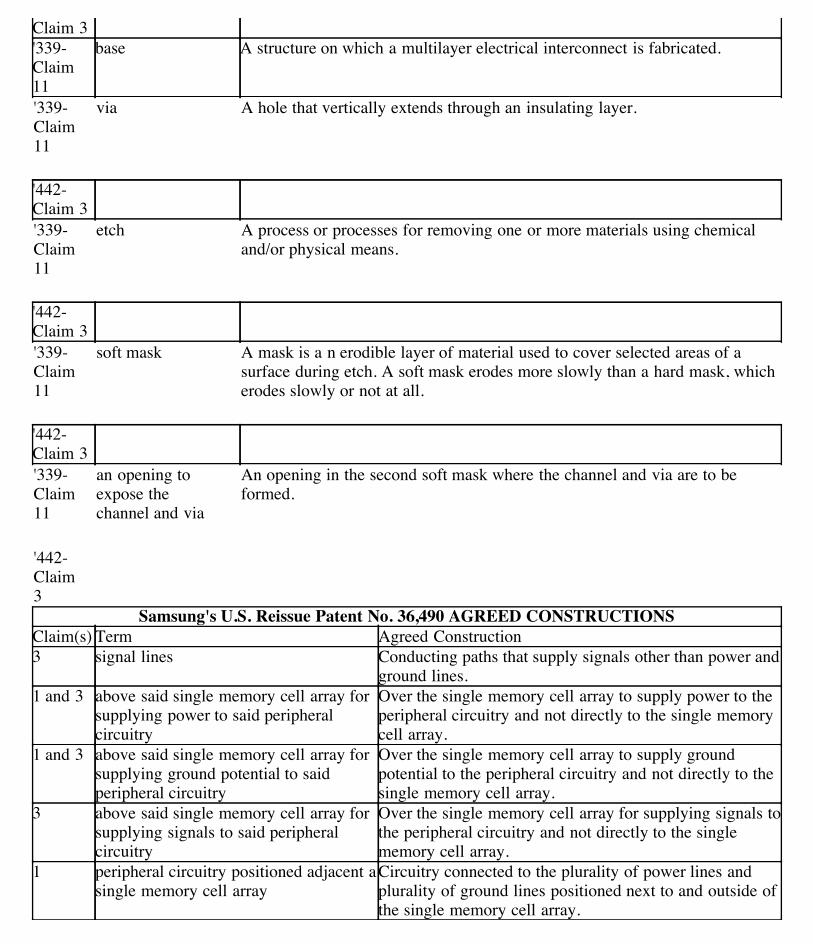
3/3/10 2:57 AMUntitled Document
Page 31 of 51file:///Users/sethchase/Desktop/Markman/htmlfiles/2007.11.14_SAM…NG_ELECTRONICS_CO_LTD_v._MATSUSHITA_ELECTRIC_INDUSTRIAL_CO.html
Claim 3'339-Claim11
base A structure on which a multilayer electrical interconnect is fabricated.
'339-Claim11
via A hole that vertically extends through an insulating layer.
'442-Claim 3'339-Claim11
etch A process or processes for removing one or more materials using chemicaland/or physical means.
'442-Claim 3'339-Claim11
soft mask A mask is a n erodible layer of material used to cover selected areas of asurface during etch. A soft mask erodes more slowly than a hard mask, whicherodes slowly or not at all.
'442-Claim 3'339-Claim11
an opening toexpose thechannel and via
An opening in the second soft mask where the channel and via are to beformed.
'442-Claim3
Samsung's U.S. Reissue Patent No. 36,490 AGREED CONSTRUCTIONSClaim(s) Term Agreed Construction3 signal lines Conducting paths that supply signals other than power and
ground lines.1 and 3 above said single memory cell array for
supplying power to said peripheralcircuitry
Over the single memory cell array to supply power to theperipheral circuitry and not directly to the single memorycell array.
1 and 3 above said single memory cell array forsupplying ground potential to saidperipheral circuitry
Over the single memory cell array to supply groundpotential to the peripheral circuitry and not directly to thesingle memory cell array.
3 above said single memory cell array forsupplying signals to said peripheralcircuitry
Over the single memory cell array for supplying signals tothe peripheral circuitry and not directly to the singlememory cell array.
1 peripheral circuitry positioned adjacent asingle memory cell array
Circuitry connected to the plurality of power lines andplurality of ground lines positioned next to and outside ofthe single memory cell array.

3/3/10 2:57 AMUntitled Document
Page 32 of 51file:///Users/sethchase/Desktop/Markman/htmlfiles/2007.11.14_SAM…NG_ELECTRONICS_CO_LTD_v._MATSUSHITA_ELECTRIC_INDUSTRIAL_CO.html
3 peripheral circuitry adjacent a saidmemory cell array
Circuitry connected to the plurality of power lines andplurality of ground lines next to and outside of saidmemory cell array.
1 each power line being substantiallyparallel to and spaced apart from everyother power line
This term requires no express construction because it canbe understood from its plain and ordinary meaning.
1 each ground line being substantiallyparallel to and spaced apart from everyother ground line
This term requires no express construction because it canbe understood from its plain and ordinary meaning.
3 substantially parallel power lines This term requires no express construction because it canbe understood from its plain and ordinary meaning.
3 substantially parallel ground lines This term requires no express construction because it canbe understood from its plain and ordinary meaning.
Samsung's U.S. Reissue Patent No. 36,490 DISPUTEDCONSTRUCTIONSClaim(s) Term Court's Construction3 memory cell
arrayA coordinated group or matrix ofmemory cells.[Agreed to at the hearing.]
1 and 3 single memory cellarray
No construction necessary.
1 and 3 power lines Conducting paths that provide electricpower.
1 and3
ground lines Conducting paths that provide aconnection to the ground.
MEI's U.S. Reissue Patent No. 35,921 & U.S. Reissue Patent No. 35,680 AGREEDCONSTRUCTIONS
Claim(s) Term Agreed Construction'921-Claim40
first bus A first set of signal lines over which information is transmitted to or from adevice.
'680-Claim 42'921-Claim40
second bus A second set of signal lines over which information is transmitted to or from adevice.
'680-Claim 42'921-Claim40
operationmode
A manner in which a device operates.
'680-

3/3/10 2:57 AMUntitled Document
Page 33 of 51file:///Users/sethchase/Desktop/Markman/htmlfiles/2007.11.14_SAM…NG_ELECTRONICS_CO_LTD_v._MATSUSHITA_ELECTRIC_INDUSTRIAL_CO.html
Claim 42'921-Claim 36
digital controlcircuit
This term requires no express construction because it can be understood from itsplain and ordinary meaning.
'921-Claims6 and9
dynamicrandom statemachine
A dynamic sequential-logic system whose outputs depend on previous and presentinputs on the random port, as opposed to processes that are functions of presentinputs alone.
'921-Claims71-73
random statemachine
A sequential-logic system whose outputs depend on previous and present inputson the random port, as opposed to processes that are functions of present inputsalone.
'680-Claims48-50'921-Claim5
addressmeans
Function: For holding a first address of information stored in said dynamicrandom access memory in response to a first edge of said external clock signal,and for holding a second address of said information stored in said dynamicrandom access memory in response to a second edge of said external clock signal.
Governed by35 U.S.C. s.112 para. 6.
Corresponding structure: address register (1320) and equivalents thereof.
'921-Claim8
addressmeans
Function: for holding a first address of information stored in said dynamic randomaccess memory in response to a first edge of said external clock signal and forholding a second address of said information stored in said dynamic randomaccess memory in response to a second edge of said external clock signal, saidfirst edge of said external clock sign b[sic] different from said second edge of saidexternal clock signal.
Governed by35 U.S.C. s.112 para. 6.
Corresponding structure: address register (1320) and equivalents thereof.
'921-Claim10
addressinput means
Function: for receiving a first address and a second address defining a location ofinformation stored in said memory block, said address input means providing saidfirst address as an output in response to a first edge of said external clock signal,said address input means providing said second address as an output in response toa second edge of said external clock signal, said first edge of said external clocksignal being different from said second edge of said external clock signal.
Governed by35 U.S.C. s.112 para. 6.
Corresponding structure: address register (1320) and equivalents thereof.
'921-Claim17
addressinput means
Function: provides said first address in response to said first enable signal, saidaddress input means provides said second address in response to said secondenable signal.

3/3/10 2:57 AMUntitled Document
Page 34 of 51file:///Users/sethchase/Desktop/Markman/htmlfiles/2007.11.14_SAM…NG_ELECTRONICS_CO_LTD_v._MATSUSHITA_ELECTRIC_INDUSTRIAL_CO.html
Governed by35 U.S.C. s.112 para. 6.
Corresponding structure: address register (1320) and equivalents thereof.
'921-Claim23
addressinput means
Function: for receiving a first address and a second address defining a location ofinformation stored in said memory block, said address input means providing saidfirst address as an output in response to a first enable signal, and said addressinput means providing said second address as an output in response to a secondenable signal.
Governed by35 U.S.C. s.112 para. 6.
Corresponding structure: address register (1320) and equivalents thereof.
'921-Claim31
addressinput means
Function: for receiving a first address and a second address defining a location ofinformation stored in said memory block.
Governed by35 U.S.C. s.112 para. 6.
Corresponding structure: address register (1320) and equivalents thereof.
'921-Claim33
addressinput means
Function: for receiving a first address and a second address defining a location ofinformation stored in said memory block.
Governed by35 U.S.C. s.112 para. 6.
Corresponding structure: address register (1320) and equivalents thereof.
'921-Claim35
addressinput means
Function: for receiving a first address and a second address defining a location ofinformation stored in said memory block.
Governed by35 U.S.C. s.112 para. 6.
Corresponding structure: address register (1320) and equivalents thereof.
'921-Claim40
addressinput means
Function: for receiving a first address and a second address through said first bus,said address input means providing said first address as an output in response to afirst edge of said external clock signal, said address input means providing saidsecond address as an output in response to a second edge of said external clocksignal, said first edge of said external clock signal being different from saidsecond edge of said external clock signal.
Governed by35 U.S.C. s.112 para. 6.
Corresponding structure: address register (1320) and equivalents thereof.
'921- address Function: provides said first address in response to said first enable signal, said

3/3/10 2:57 AMUntitled Document
Page 35 of 51file:///Users/sethchase/Desktop/Markman/htmlfiles/2007.11.14_SAM…NG_ELECTRONICS_CO_LTD_v._MATSUSHITA_ELECTRIC_INDUSTRIAL_CO.html
Claim42
input means address input means provides said second address in response to said secondenable signal.
Governed by35 U.S.C. s.112 para. 6.
Corresponding structure: address register (1320) and equivalents thereof.
'921-Claim53
addressinput means
Function: for receiving a first address and a second address, said address inputmeans providing said first address as an output in response to an edge of saidexternal clock signal, said address input means providing said second address asan output in response to an edge of said external clock signal.
Governed by35 U.S.C. s.112 para. 6.
Corresponding structure: address register (1320) and equivalents thereof.
'921-Claim66
addressinput means
Function: for receiving a first address and a second address, said address inputmeans providing said first address as an output in response to a first edge of saidexternal clock input, said address input means providing said second address as anoutput in response to a second edge of said external clock input, said first edge ofsaid external clock input being different from said second edge of said externalclock input.
Governed by35 U.S.C. s.112 para. 6.
Corresponding structure: address register (1320) and equivalents thereof.
'921-Claim68
addressinput means
Function: for receiving a first address and a second address, said address inputmeans providing said first address as an output in response to a first enable signal,said address input means providing said second address as an output in response toa second enable signal.
Governed by35 U.S.C. s.112 para. 6.
Corresponding structure: address register (1320) and equivalents thereof.
'921-Claim71
addressinput means
Function: for receiving a first address and a second address, said address inputmeans providing said first address as an output in response to an edge of saidexternal clock signal, said address input means providing said second address asan output in response to an edge of said external clock signal.
Governed by35 U.S.C. s.112 para. 6.
Corresponding structure: address register (1320) and equivalents thereof.
'921-Claim75
addressinput means
Function: for receiving a first address and a second address, said address inputmeans providing said first address as an output in response to a first edge of saidexternal clock signal, said address input means providing said second address asan output in response to a second edge of said external clock signal, said firstedge of said external clock signal being different from said second edge of said

3/3/10 2:57 AMUntitled Document
Page 36 of 51file:///Users/sethchase/Desktop/Markman/htmlfiles/2007.11.14_SAM…NG_ELECTRONICS_CO_LTD_v._MATSUSHITA_ELECTRIC_INDUSTRIAL_CO.html
external clock signal.
Governed by35 U.S.C. s.112 para. 6.
Corresponding structure: address register (1320) and equivalents thereof.
'680-Claim35
addressinput means
Function: for receiving and holding said first address from said bus in response tosaid first edge of said clock signal and for receiving and holding said secondaddress from said bus in response to said second edge of said clock signal.
Governed by35 U.S.C. s.112 para. 6.
Corresponding structure: address register (1320) and equivalents thereof.
'680-Claim37
addressinput means
Function: holds said first address based on said first enable signal, said addressinput means holds said second address based on said second enable signal.
Governed by35 U.S.C. s.112 para. 6.
Corresponding structure: address register (1320) and equivalents thereof.
'921-Claim5
outputmeans
Function: for delivering said stored information at said first and second addressesfrom said memory to said data bus.
Governed by35 U.S.C. s.112 para. 6.
Corresponding Structure: output control (1338) and equivalents thereof.
'921-Claim8
outputmeans
Function: For delivering said stored information at said first and second addressesfrom said memory block to said data bus.
Governed by35 U.S.C. s.112 para. 6.
Corresponding Structure: output control (1338) and equivalents thereof.
'921-Claim11
outputmeans
Function: for outputting information stored at said location of said memory blockin response to a third edge of said external clock signal.
Governed by35 U.S.C. s.112 para. 6.
Corresponding Structure: output control (1338) and equivalents thereof.
'921-Claim17
outputmeans
Function: outputs said information in response to said output enable signal.
Governed by Corresponding Structure: output control (1338) and equivalents thereof.

3/3/10 2:57 AMUntitled Document
Page 37 of 51file:///Users/sethchase/Desktop/Markman/htmlfiles/2007.11.14_SAM…NG_ELECTRONICS_CO_LTD_v._MATSUSHITA_ELECTRIC_INDUSTRIAL_CO.html
35 U.S.C. s.112 para. 6.
'921-Claim29
outputmeans
Function: for outputting information stored at said location of said memory blockin response to an output enable signal.
Governed by35 U.S.C. s.112 para. 6.
Corresponding Structure: output control (1338) and equivalents thereof.
'921-Claim31
outputmeans
Function: for outputting information from said memory block.
Governed by35 U.S.C. s.112 para. 6.
Corresponding Structure: output control (1338) and equivalents thereof.
'921-Claim35
outputmeans
Function: for outputting information from said memory block.
Governed by35 U.S.C. s.112 para. 6.
Corresponding Structure: output control (1338) and equivalents thereof.
'921-Claim36
outputmeans
Function: for outputting said information read from said memory to a data bus inresponse to an output enable signal.
Governed by35 U.S.C. s.112 para. 6.
Corresponding Structure: output control (1338) and equivalents thereof.
'921-Claim59
outputmeans
Function: for outputting information stored at said location of said memory blockin response to a third edge of said external clock signal.
Governed by35 U.S.C. s.112 para. 6.
Corresponding Structure: output control (1338) and equivalents thereof.
'680-Claim36
outputmeans
Function: for outputting to said bus, information stored at said location of saidmemory block in response to a third edge of said clock signal.
Governed by35 U.S.C. s.112 para. 6.
Corresponding Structure: output control (1338) and equivalents thereof.
'921- write mask Function: for generating a write prohibition signal for prohibiting writing

3/3/10 2:57 AMUntitled Document
Page 38 of 51file:///Users/sethchase/Desktop/Markman/htmlfiles/2007.11.14_SAM…NG_ELECTRONICS_CO_LTD_v._MATSUSHITA_ELECTRIC_INDUSTRIAL_CO.html
Claim12
means information to at least one bit location in said memory block based on said maskinformation.
Governed by35 U.S.C. s.112 para. 6.
Corresponding structure: write mask (1336) and equivalents thereof.
'921-Claim7
data inputmeans
Function: for receiving data and for holding said data in response to an edge ofsaid external clock signal.
Governed by35 U.S.C. s.112 para. 6.
Corresponding structure: data register (1340) and equivalents thereof.
'921-Claim18
data inputmeans
Function: for receiving data, said data input means providing said data as anoutput in response to an edge of said external clock signal.
Governed by35 U.S.C. s.112 para. 6.
Corresponding structure: data register (1340) and equivalents thereof.
'921-Claim19
data inputmeans
Function: provides said data in response to said data enable signal.
Governed by35 U.S.C. s.112 para. 6.
Corresponding structure: data register (1340) and equivalents thereof.
'921-Claim24
data inputmeans
Function: for receiving data, said data input means providing said data as anoutput in response to a data enable signal.
Governed by35 U.S.C. s.112 para. 6.
Corresponding structure: data register (1340) and equivalents thereof.
'921-Claim33
data inputmeans
Function: for receiving data.
Governed by35 U.S.C. s.112 para. 6.
Corresponding structure: data register (1340) and equivalents thereof.
'921-Claim35
data inputmeans
Function: for receiving data.

3/3/10 2:57 AMUntitled Document
Page 39 of 51file:///Users/sethchase/Desktop/Markman/htmlfiles/2007.11.14_SAM…NG_ELECTRONICS_CO_LTD_v._MATSUSHITA_ELECTRIC_INDUSTRIAL_CO.html
Governed by35 U.S.C. s.112 para. 6.
Corresponding structure: data register (1340) and equivalents thereof.
'921-Claim61
data inputmeans
Function: for receiving data, said data input means providing said data as anoutput in response to a third edge of said external clock signal.
Governed by35 U.S.C. s.112 para. 6.
Corresponding structure: data register (1340) and equivalents thereof.
'921-Claim36
[outputting]means
Function: for outputting said information read from said memory to a data bus inresponse to an output enable signal.
Governed by35 U.S.C. s.112 para. 6.
Corresponding structure: output control (1338) and equivalents thereof.
'921-Claim12
maskinformationinput means
Function: for receiving mask information, said mask information input meansproviding said mask information as an output in response to a third edge of saidexternal clock signal.
Governed by35 U.S.C. s.112 para. 6.
Corresponding Structure: data register 1340.
'921-Claim36
[reading]means
Function: for reading information stored at said addressable memory location
Governed by35 U.S.C. s.112 para. 6.
Corresponding Structure: block decode 1330.
'921-Claim5
controlmeans
Function: for receiving said external clock signal from said control bus and beingfurther connected to said address means, said output means and said dynamicrandom access memory, said control means being responsive to the receipt of saidexternal clock signal for controlling the operation of said address means, saidoutput means, and said dynamic random access memory.
Governed by35 U.S.C. s.112 para. 6.
Corresponding Structure: Random state machine (1366)
'921-Claim8
controlmeans
Function: for holding a first address of information stored in said dynamic randomaccess memory in response to a first edge of said external clock signal and forholding a second address of said information stored in said dynamic randomaccess memory in response to a second edge of said external clock signal, saidfirst edge of said external clock sign b[sic] different from said second edge of said

3/3/10 2:57 AMUntitled Document
Page 40 of 51file:///Users/sethchase/Desktop/Markman/htmlfiles/2007.11.14_SAM…NG_ELECTRONICS_CO_LTD_v._MATSUSHITA_ELECTRIC_INDUSTRIAL_CO.html
external clock signal.
Governed by35 U.S.C. s.112 para. 6.
Corresponding Structure: Random state machine (1366)
'921-Claim17
controlmeans
Function: for supplying a first enable signal and a second enable signal to saidaddress input means in response to an external control input on an edge of saidexternal clock signal, and for supplying an output enable signal to said outputmeans in response to said external control input on an edge of said external clocksignal, each of said first enable signal, said second enable signal and said outputenable signal being synchronous with an edge of said external clock signal.
Governed by35 U.S.C. s.112 para. 6.
Corresponding Structure: Random state machine (1366)
'921-Claim19
controlmeans
Function: for supplying a data enable signal to said data input means in responseto an external control input on an edge of said external clock signal, and forsupplying awrite enable signal to said write means in response to said externalcontrol input on an edge of said external clock signal, each of said data enablesignal and said write enablesignal being synchronous with an edge of said externalclock signal.
Governed by35 U.S.C. s.112 para. 6.
Corresponding Structure: Random state machine (1366)
'921-Claim23
controlmeans
Function: for supplying said first enable signal and said second enable signal tosaid address input means in response to an external control input on an edge ofsaidexternal clock signal, and for supplying said output enable signal to saidoutput means in response to said external control input on an edge of said externalclock signal, each of said first enable signal, said second enable signal and saidoutput enable signal being synchronous with an edge of said external clock signal.
Governed by35 U.S.C. s.112 para. 6.
Corresponding Structure: Random state machine (1366)
'921-Claim24
controlmeans
Function: supplies said data enable signal to said data input means in response tosaid external control input on an edge of said external clock signal, and suppliessaid write enable signal to said write means in response to said external controlinput on an edge of said external clock signal, each of said data enable signal andsaid write enable signal being synchronous with an edge of said external clocksignal.
Governed by35 U.S.C. s.112 para. 6.
Corresponding Structure: Random state machine (1366)
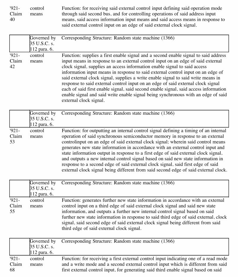
3/3/10 2:57 AMUntitled Document
Page 41 of 51file:///Users/sethchase/Desktop/Markman/htmlfiles/2007.11.14_SAM…NG_ELECTRONICS_CO_LTD_v._MATSUSHITA_ELECTRIC_INDUSTRIAL_CO.html
'921-Claim40
controlmeans
Function: for receiving said external control input defining said operation modethrough said second bus, and for controlling operations of said address inputmeans, said access information input means and said access means in response tosaid external control input on an edge of said external clock signal.
Governed by35 U.S.C. s.112 para. 6.
Corresponding Structure: Random state machine (1366)
'921-Claim42
controlmeans
Function: supplies a first enable signal and a second enable signal to said addressinput means in response to an external control input on an edge of said externalclock signal, supplies an access information enable signal to said accessinformation input means in response to said external control input on an edge ofsaid external clock signal, supplies a write enable signal to said write means inresponse to said external control input on an edge of said external clock signaleach of said first enable signal, said second enable signal, said access informationenable signal and said write enable signal being synchronous with an edge of saidexternal clock signal.
Governed by35 U.S.C. s.112 para. 6.
Corresponding Structure: Random state machine (1366)
'921-Claim53
controlmeans
Function: for outputting an internal control signal defining a timing of an internaloperation of said synchronous semiconductor memory in response to an externalcontrolinput on an edge of said external clock signal; wherein said control meansgenerates new state information in accordance with an external control input andstate information output in response to a first edge of said external clock signal,and outputs a new internal control signal based on said new state information inresponse to a second edge of said external clock signal, said first edge of saidexternal clock signal being different from said second edge of said external clock.
Governed by35 U.S.C. s.112 para. 6.
Corresponding Structure: Random state machine (1366)
'921-Claim55
controlmeans
Function: generates further new state information in accordance with an externalcontrol input on a third edge of said external clock signal and said new stateinformation, and outputs a further new internal control signal based on saidfurther new state information in response to said third edge of said external, clocksignal, said second edge of said external clock signal being different from saidthird edge of said external clock signal.
Governed by35 U.S.C. s.112 para. 6.
Corresponding Structure: Random state machine (1366)
'921-Claim68
controlmeans
Function: for receiving a first external control input indicating one of a read modeand a write mode and a second external control input which is different from saidfirst external control input, for generating said third enable signal based on said

3/3/10 2:57 AMUntitled Document
Page 42 of 51file:///Users/sethchase/Desktop/Markman/htmlfiles/2007.11.14_SAM…NG_ELECTRONICS_CO_LTD_v._MATSUSHITA_ELECTRIC_INDUSTRIAL_CO.html
first external control input and generating at least one of said first enable signaland said second enable signal based on said second external control input, and forsupplying said third enable signal to said access means in response to an edge ofsaid external clock signal and supplying at least one of said first enable signal andsaid second enable signal to said address input means in response to an edge ofsaid external clock signal.
Governed by35 U.S.C. s.112 para. 6.
Corresponding Structure: Random state machine (1366)
'921-Claim71
controlmeans
Function: for outputting an internal control signal defining a timing of an internaloperation of said synchronous semiconductor memory in response to an externalcontrol input on an edge of said external clock signal; wherein said control meanscomprises a random state machine.
Governed by35 U.S.C. s.112 para. 6.
Corresponding Structure: Random state machine (1366)
'921-Claim75
controlmeans
Function: for receiving a predetermined set of control signals provided fromoutside of said synchronous dynamic random access memory, for making atransition from a state to a next state in accordance with said predetermined set ofcontrol signals on respective edges of said external clock signal, and foroutputting an internal control signal defining a timing of an internal operation ofsaid synchronous dynamic random access memory based on the said next state.
Governed by35 U.S.C. s.112 para. 6.
Corresponding Structure: Random state machine (1366)
'680-Claim37
controlmeans
Function: for supplying a first enable signal and a second enable signal to saidaddress input means in response to said control input on an edge of said clocksignal, and for supplying an output enable signal to said output means in responseto said control input on an edge of said clock signal, each of said first enablesignal, said second enable signal and said output enable signal being synchronouswith an edge of said clock signal.
Governed by35 U.S.C. s.112 para. 6.
Corresponding Structure: Random state machine (1366)
'680-Claim39
controlmeans
Function: for supplying a data enable signal to said data input means in responseto said control input on an edge of said clock signal, and for supplying a writeenable signal to said write means in response to said control input on an edge ofsaid clock signal, each of said data enable signal and said write enable signalbeing synchronous with an edge of said clock signal.
Governed by Corresponding Structure: Random state machine (1366)

3/3/10 2:57 AMUntitled Document
Page 43 of 51file:///Users/sethchase/Desktop/Markman/htmlfiles/2007.11.14_SAM…NG_ELECTRONICS_CO_LTD_v._MATSUSHITA_ELECTRIC_INDUSTRIAL_CO.html
35 U.S.C. s.112 para. 6.
'680-Claim42
controlmeans
Function: for receiving said control input through said second bus, and forcontrolling operations of said address input means, said access information inputmeans and said access means in response to said control input on an edge of saidclock signal.
Governed by35 U.S.C. s.112 para. 6.
Corresponding Structure: Random state machine (1366)
'680-Claim45
controlmeans
Function: for outputting an internal control signal defining a timing of an internaloperation of said synchronous dynamic random access memory based on a controlinput on an edge of said clock signal; wherein said control means generates newstate information in accordance with a control input and state information outputin response to a third edge of said clock signal, and outputs a new internal controlsignal based on said new state information in response to a fourth edge of saidclock signal, said third edge of said clock signal being different from said fourthedge of said clock signal.
Governed by35 U.S.C. s.112 para. 6.
Corresponding Structure: Random state machine (1366)
'680-Claim51
controlmeans
Function: for receiving a predetermined set of control signals provided fromoutside of said memory, for transitioning from one state to at least one next statein accordance with said predetermined set of control signals on respective edgesof said clock signal, and for outputting internal control signals defining timings ofinternal operations of said memory based on the at least one next state.
Governed by35 U.S.C. s.112 para. 6.
Corresponding Structure: Random state machine (1366)
'921-Claim26
[next statedetermining]means
Function: for determining a next state in response to a current state and saidexternal control input on an edge of said external clock signal.
Governed by35 U.S.C. s.112 para. 6.
Corresponding Structure: random state machine 1366.
'921-Claim27
[next statedetermining]means
Function: for determining a next state in response to a current state and saidexternal control input on an edge of said external clock signal.
Governed by35 U.S.C. s.112 para. 6.
Corresponding Structure: random state machine 1366.

3/3/10 2:57 AMUntitled Document
Page 44 of 51file:///Users/sethchase/Desktop/Markman/htmlfiles/2007.11.14_SAM…NG_ELECTRONICS_CO_LTD_v._MATSUSHITA_ELECTRIC_INDUSTRIAL_CO.html
'921-Claim26
[producing]means
Function: for producing said first enable signal, said second enable signal, saidoutput enable signal, said data enable signal and said write enable signal as afunction of said next state.
Governed by35 U.S.C. s.112 para. 6.
Corresponding Structure: state machine 1366.
'921-Claim27
[producing]means
Function: for producing said first enable signal, said second enable signal and saidoutput enable signal as a function of said next state.
Governedby 35U.S.C. s.112 para. 6.
Corresponding Structure: state machine 1366.
MEI's U.S. Reissue Patent No. 35,921 & U.S. Reissue Patent No. 35,680 DISPUTEDCONSTRUCTIONS
Claim(s) Term Court's Construction'921-Claims 5-12,16-20, 23, 24, 26,28, 31, 33, 35, 36,38, 40-42, 48-50,53-55, 59, 61, 65,68, 69, 71, 72 and75
external clock signal A single timing signal from outside of a device.
'680-Claims 35-39,42, 45, 48, 49, and51
clock signal A single timing signal.
'921-Claims 40and 42
access information Information that specifies a memory access.
'680-Claim 42'921-Claim 40 access information
defining a specification ofsaid operation mode.
Information defining a specification for an operationmode.
'680-Claim 42'921-Claim 40 access information defining a
specification of said operationmode in combination withsaid external control inputdefining said operationspecifics of the operationmode.
Information defining a specification for an operationmode, which, together with external control input,defines the mode.
'921-Claim 66 output means Function: sequentially outputting a plurality of datawhich belong to separately addressable locations in saidmemory blocks at substantially a same interval, saidplurality of data including data stored at a location insaid memory blocks corresponding to said first address

3/3/10 2:57 AMUntitled Document
Page 45 of 51file:///Users/sethchase/Desktop/Markman/htmlfiles/2007.11.14_SAM…NG_ELECTRONICS_CO_LTD_v._MATSUSHITA_ELECTRIC_INDUSTRIAL_CO.html
and said second address provided by said address inputmeans. [Agreed]
Governed by 35 U.S.C. s. 112para. 6.
Corresponding Structure: Dynamic latch 1304, serial dataport 1306, and output control 1338.
'680-Claim 47 output means Function: sequentially outputting a plurality of datawhich belong to separately addressable locations in saidindividual memory blocks at substantially a sameinterval, said plurality of data including data stored at alocation in said memory block corresponding to said firstaddress and said second address. [Agreed.]
Governed by 35 U.S.C. s. 112para. 6.
Corresponding Structure: Dynamic latch 1304, serial dataport 1306, and output control 1338.
'921-Claim 10 access means Function: for accessing a location in said memory blockcorresponding to said first address and said secondaddress provided by said address input means. [Agreed.]
Governed by 35 U.S.C. s. 112para. 6.
Corresponding Structure: output control 1338, write mask1336, and drawing rule 1354.
'921-Claim 23 access means Function: for accessing a location in said memory blockcorresponding to said first address and said secondaddress provided by said address input means. [Agreed.]
Governed by 35 U.S.C. s. 112para. 6.
Corresponding Structure: output control 1338, write mask1336, and drawing rule 1354.
'921-Claim 40 access means Function: for accessing a location in said memory blockcorresponding to said first address and said secondaddress provided by said address input means inaccordance with said operation mode. [Agreed.]
Governed by 35 U.S.C. s. 112para. 6.
Corresponding Structure: output control 1338, write mask1336, and drawing rule 1354.
'921-Claim 53 access means Function: for accessing a location in said memory blockcorresponding to said first address and said secondaddress provided by said address input means. [Agreed.]
Governed by 35 U.S.C. s. 112para. 6.
Corresponding Structure: output control 1338, write mask1336, and drawing rule 1354.
'921-Claim 68 access means Function: for accessing a location in said memory blockcorresponding to said first address and said secondaddress provided by said address input means in responseto a third enable signal. [Agreed.]
Governed by 35 U.S.C. s. 112 Corresponding Structure: output control 1338, write mask

3/3/10 2:57 AMUntitled Document
Page 46 of 51file:///Users/sethchase/Desktop/Markman/htmlfiles/2007.11.14_SAM…NG_ELECTRONICS_CO_LTD_v._MATSUSHITA_ELECTRIC_INDUSTRIAL_CO.html
para. 6. 1336, and drawing rule 1354.'921-Claim 71 access means Function: for accessing a location in said memory block
corresponding to said first address and said secondaddress provided by said address input means. [Agreed.]
Governed by 35 U.S.C. s. 112para. 6.
Corresponding Structure: output control 1338, write mask1336, and drawing rule 1354.
'921-Claim 75 access means Function: for accessing a location in said memory blockcorresponding to said first address and said secondaddress provided by said address input means. [Agreed.]
Governed by 35 U.S.C. s. 112para. 6.
Corresponding Structure: output control 1338, write mask1336, and drawing rule 1354.
'680-Claim 35 access means Function: for accessing a location in said memory blockcorresponding to said first address and said secondaddress held by said address input means. [Agreed.]
Governed by 35 U.S.C. s. 112para. 6.
Corresponding Structure: output control 1338, write mask1336, and drawing rule 1354.
'921-Claim 7 writing means/writemeans/means for writing
Function: for writing said held data to said memory.[Agreed.]
Governed by 35 U.S.C. s. 112para. 6.
Corresponding Structure: write mask 1336 and drawingrule 1354.
'921-Claim 12 writing means/writemeans/means for writing
Function: for writing said information to said memoryblock in accordance with said write prohibition signalwithin a region in said memory block corresponding tosaid first address and said second address provided bysaid address input means. [Agreed.]
Governed by 35 U.S.C. s. 112para. 6.
Corresponding Structure: write mask 1336 and drawingrule 1354.
'921-Claim 16 writing means/writemeans/means for writing
Function: writes said information to said memory blockin response to a fourth edge of said external clock signal.[Agreed.]
Governed by 35 U.S.C. s. 112para. 6.
Corresponding Structure: write mask 1336 and drawingrule 1354.
'921-Claim 18 writing means/writemeans/means for writing
Function: for writing said data to said memory block at alocation addressed by said first address and said secondaddress in response to an edge of said external clocksignal. [Agreed.]
Governed by 35 U.S.C. s. 112 Corresponding Structure: write mask 1336 and drawing

3/3/10 2:57 AMUntitled Document
Page 47 of 51file:///Users/sethchase/Desktop/Markman/htmlfiles/2007.11.14_SAM…NG_ELECTRONICS_CO_LTD_v._MATSUSHITA_ELECTRIC_INDUSTRIAL_CO.html
para. 6. rule 1354.'921-Claim 24 writing means/write
means/means for writingFunction: for writing said data to said memory block at alocation addressed by said first address and said secondaddress in response to a write enable signal. [Agreed.]
Governed by 35 U.S.C. s. 112para. 6.
Corresponding Structure: write mask 1336 and drawingrule 1354.
'921-Claim 33 writing means/writemeans/means for writing
Function: for writing said data into said memory block.[Agreed.]
Governed by 35 U.S.C. s. 112para. 6.
Corresponding Structure: write mask 1336 and drawingrule 1354.
'921-Claim 35 writing means/writemeans/means for writing
Function: for writing said data into said memory block.[Agreed.]
Governed by 35 U.S.C. s. 112para. 6.
Corresponding Structure: write mask 1336 and drawingrule 1354.
'921-Claim 38 writing means/writemeans/means for writing
Function: for writing said data loaded in said data bufferto said addressable memory location represented by saidaddress loaded in said address buffer. [Agreed.]
Governed by 35 U.S.C. s. 112para. 6.
Corresponding Structure: write mask 1336 and drawingrule 1354.
'921-Claim 41 writing means/writemeans/means for writing
Function: for writing information to said memory blockat a location corresponding to said first and said secondaddress in response to a fourth edge of said externalclock signal. [Agreed.]
Governed by 35 U.S.C. s. 112para. 6.
Corresponding Structure: write mask 1336 and drawingrule 1354.
'921-Claim 42 writing means/writemeans/means for writing
Function: writes said information in response to saidwrite enable signal. [Agreed.]
Governed by 35 U.S.C. s. 112para. 6.
Corresponding Structure: write mask 1336 and drawingrule 1354.
'921-Claim 61 writing means/writemeans/means for writing
Function: for writing said data to said memory block at alocation corresponding to said first and said secondaddress in response to a fourth edge of said externalclock signal. [Agreed.]
Governed by 35 U.S.C. s. 112para. 6.
Corresponding Structure: write mask 1336 and drawingrule 1354.
'680-Claim 38 writing means/writemeans/means for writing
Function: for writing said data to said memory block atsaid location corresponding to said first address and said

3/3/10 2:57 AMUntitled Document
Page 48 of 51file:///Users/sethchase/Desktop/Markman/htmlfiles/2007.11.14_SAM…NG_ELECTRONICS_CO_LTD_v._MATSUSHITA_ELECTRIC_INDUSTRIAL_CO.html
second address in response to a fourth edge of said clocksignal. [Agreed.]
Governed by 35 U.S.C. s. 112para. 6.
Corresponding Structure: write mask 1336 and drawingrule 1354.
'921-Claim 40 access information inputmeans
Function: for receiving access information through saidfirst bus. [Agreed.]
Governed by 35 U.S.C. s. 112para. 6.
Corresponding Structure: address register 1320 and dataregister 1340.
'921-Claim 42 access information inputmeans
Function: provides said access information in response tosaid access information enable signal. [Agreed.]
Governed by 35 U.S.C. s. 112para. 6.
Corresponding Structure: address register 1320 and dataregister 1340.
'680-Claim 42 access information inputmeans
Function: for receiving said access information throughsaid first bus and providing said access information as anoutput in response to said third edge of said clock signal.[Agreed.]
Governed by 35 U.S.C. s. 112para. 6.
Corresponding Structure: address register 1320 and dataregister 1340.
'921-Claim 73 decoding means Function: for decoding said new state so as to output saidinternal control signal. [Agreed.]
Governed by 35 U.S.C. s. 112para. 6.
Corresponding Structure: state machine 1366.
'680-Claim 50 decoding means Function: for decoding said new state so as to output saidinternal control signal. [Agreed.]
Governed by 35 U.S.C. s. 112para. 6.
Corresponding Structure: state machine 1366.
'680-Claim 35 address providing means Function: for providing a first address and a secondaddress on said bus, said first address being valid on saidbus on a first edge of a clock signal and said secondaddress being valid on said bus on a second edge of saidclock signal, said first edge of said clock signal beingdifferent from said second edge of said clock signal.[Agreed.]
Governed by 35 U.S.C. s. 112para. 6.
Corresponding Structure: a processor (CPU), a bus 170,and an interface circuit 160.
'680-Claim 38 data providing means Function: for providing data on said bus which is validon a third edge of said clock signal. [Agreed.]

3/3/10 2:57 AMUntitled Document
Page 49 of 51file:///Users/sethchase/Desktop/Markman/htmlfiles/2007.11.14_SAM…NG_ELECTRONICS_CO_LTD_v._MATSUSHITA_ELECTRIC_INDUSTRIAL_CO.html
Governed by 35 U.S.C. s. 112para. 6.
Corresponding Structure: a processor (CPU), a bus 170,and an interface circuit 160.
'680-Claim 37 control input providingmeans
Function: for providing on said bus a control input, saidcontrol input being valid on an edge of said clock signal.[Agreed.]
Governed by 35 U.S.C. s. 112para. 6.
Corresponding Structure: a processor (CPU), a bus 170,and an interface circuit 160.
'680-Claim 39 control input providingmeans
Function: for providing on said bus a control input, saidcontrol input being valid on an edge of said clock signal.[Agreed.]
Governed by 35 U.S.C. s. 112para. 6.
Corresponding Structure: a processor (CPU), a bus 170,and an interface circuit 160.
'680-Claim 42 control input providingmeans
Function: for providing said control input on said secondbus ... and said control input being valid on said secondbus on an edge of said clock signal. [Agreed.]
Governed by 35 U.S.C. s. 112para. 6.
Corresponding Structure: a processor (CPU), a bus 170,and an interface circuit 160.
'680-Claim 45 control input providingmeans
Function: for providing a control input on said bus, saidcontrol input being valid on said bus on an edge of saidclock signal. [Agreed.]
Governed by 35 U.S.C. s. 112para. 6.
Corresponding Structure: a processor (CPU), a bus 170,and an interface circuit 160.
'680-Claim 48 control input providingmeans
Function: for providing a control input on said bus, saidcontrol input being valid on said bus on an edge of saidclock signal. [Agreed.]
Governed by 35 U.S.C. s. 112para. 6.
Corresponding Structure: a processor (CPU), a bus 170,and an interface circuit 160.
'680-Claim 42 access informationproviding means
Function: for providing access information defining aspecification of said operation mode on said first bus,said access information being valid on said first bus on athird edge of said clock signal. [Agreed.]
Governed by 35 U.S.C. s.112 para. 6.
Corresponding Structure: a processor (CPU), a bus 170,and an interface circuit 160.
MEI's U.S. Patent No. 5,189,588 AGREED CONSTRUCTIONSClaim(s) Term Agreed Construction2 longitudinal direction Along the length.1 and 2 diode A device that allows current to flow from the

3/3/10 2:57 AMUntitled Document
Page 50 of 51file:///Users/sethchase/Desktop/Markman/htmlfiles/2007.11.14_SAM…NG_ELECTRONICS_CO_LTD_v._MATSUSHITA_ELECTRIC_INDUSTRIAL_CO.html
anode to the cathode and inhibits current flow inthe opposite direction.
2 disposed sporadically This term requires no express constructionbecause it can be understood from its plain andordinary meaning.
2 a means for respectively connecting said pluralsignal input/output pads and said first andsecond power supply wires to the internalcircuit
Function: for respectively connecting said pluralsignal input/output pads and said first andsecond power supply wires to the internal circuit.
Governed by 35 U.S.C. s. 112 para. 6. Corresponding structure: wires as illustrated infigures 1, 2, 3, 5, 6, 7, 8, 9, 10, 11, 12 andequivalents thereof.
MEI's U.S. Patent No. 5,189,588 DISPUTED CONSTRUCTIONSClaim(s) Term Court's Construction1 protective MOS
transistorA MOS transistor that provides a discharge path for current to flow from thefirst power supply terminal to the second power supply terminal when activatedby a voltage on the drain that exceeds a predetermined level.
2 peripheral regionof thesemiconductorchip
Region outside the area of the semiconductor chip in which the internal circuitis formed.
2 plural protectivetransistors
Multiple transistors which provide a discharge path for current to flow betweenthe first power supply wire and the second power supply wire when activated.
3 protectivetransistor
A transistor which provides a discharge path for current to flow between thefirst power supply wire and the second power supply wire when activated.
1 and2
internal circuit The internal circuit which is protected by the surge protection apparatus.
MEI's U.S. Patent No. 6,677,195 AGREED CONSTRUCTIONSClaim(s) Term Agreed Construction1 connected to In direct contact with.5, 6, 8, 9 main conducting metal layer A metal layer which conducts a substantial portion of the
current.1 contact hole A vertical hole that allows electrical contact.1 fuse portion which is configured
by a metal wiring layerA portion of the metal wiring layer that can be disconnectedto cause an open circuit.
1, 2, 5-10, 17-21
metal wiring layer This term requires no express construction because it can beunderstood from its plain and ordinary meaning.
MEI's U.S. Patent No. 6,677,195 DISPUTED CONSTRUCTIONSClaim(s) Term Court's Construction1, 2, 7and 10
plug electrode A metal conductor formed in a contacthole, which connects two layers.
1, 2, 5-10, 17-21
formed on said layer insulating film No construction necessary.

3/3/10 2:57 AMUntitled Document
Page 51 of 51file:///Users/sethchase/Desktop/Markman/htmlfiles/2007.11.14_SAM…NG_ELECTRONICS_CO_LTD_v._MATSUSHITA_ELECTRIC_INDUSTRIAL_CO.html
2 formed in a plural number Two or more plug electrodes are formed.2 plug electrodes are connected respectively to both
sides which are positioned across a part of said fuseportion where cutting off is to be performed
At least one plug electrode connected tothe fuse portion on each side of the regionwhere the fuse may be cut.
Produced by Sans Paper, LLC.