max391 spee-sitchin cloc generator ith poer ail · general description the max7391 replaces ceramic...
TRANSCRIPT
General DescriptionThe MAX7391 replaces ceramic resonators, crystals, and supervisory functions for microcontrollers in 3.3V and 5V applications.The MAX7391 provides a clock source, reset, and power-fail functions. The programmable power-fail function pro-vides early warning of power failure and is configurable to detect either an external voltage or the VCC supply to the device.The clock output can be switched between normal and half-speed operation. This functionality allows the micro-controller to operate at reduced power and may be used to extend the time available to perform housekeeping tasks, such as writing data to flash during a power fail-ure. Connecting the power-fail output to the SPEED input reduces clock speed automatically during power-fail events.The MAX7391 clock output is factory programmed to a frequency in the 1MHz to 16MHz range. Four standard frequencies are available. Other frequencies are available upon request. The maximum operating supply current is 5.5mA (typ) with a clock frequency of 12MHz. Unlike typical crystal and ceramic resonator oscillator circuits, the MAX7391 is resistant to EMI and vibration, and operates reliably at high temperatures. The highout-put drive current and absence of high-impedance nodes make the oscillator invulnerable to dirty or humid operat-ing conditions.The MAX7391 is available in an 8-pin μMAX® package. The MAX7391 standard operating temperature range is from -40°C to +125°C.
Applications ● White Goods ● Appliances and Controls ● Handheld Products ● Portable Equipment ● Microcontroller Systems
Benefits and Features ● Robust Microcontroller Clock and Supervisory
Functions in a Single Package ● Integrated Reset and Power-Fail Functions ● Speed Select ● +2.7V to +5.5V Operation ● Factory-Trimmed Oscillator ● Reset Valid Down to 1.1V Supply Voltage ● ±10mA Clock-Output Drive Current ● ±4% Total Accuracy for -40°C to +125°C ● ±2.75% Total Accurac for 0°C to +85°C ● 5.5mA Operating Current (12MHz Version) ● -40°C to +125°C Temperature Range ● Surface-Mount Package ● 1MHz to 16MHz Factory Preset Frequency Range
μMAX is a registered trademark of Maxim Integrated Products, Inc.
Typical Application Circuit, Functional Diagram, and Selector Guide appear at end of data sheet.
19-3981; Rev 1; 4/14
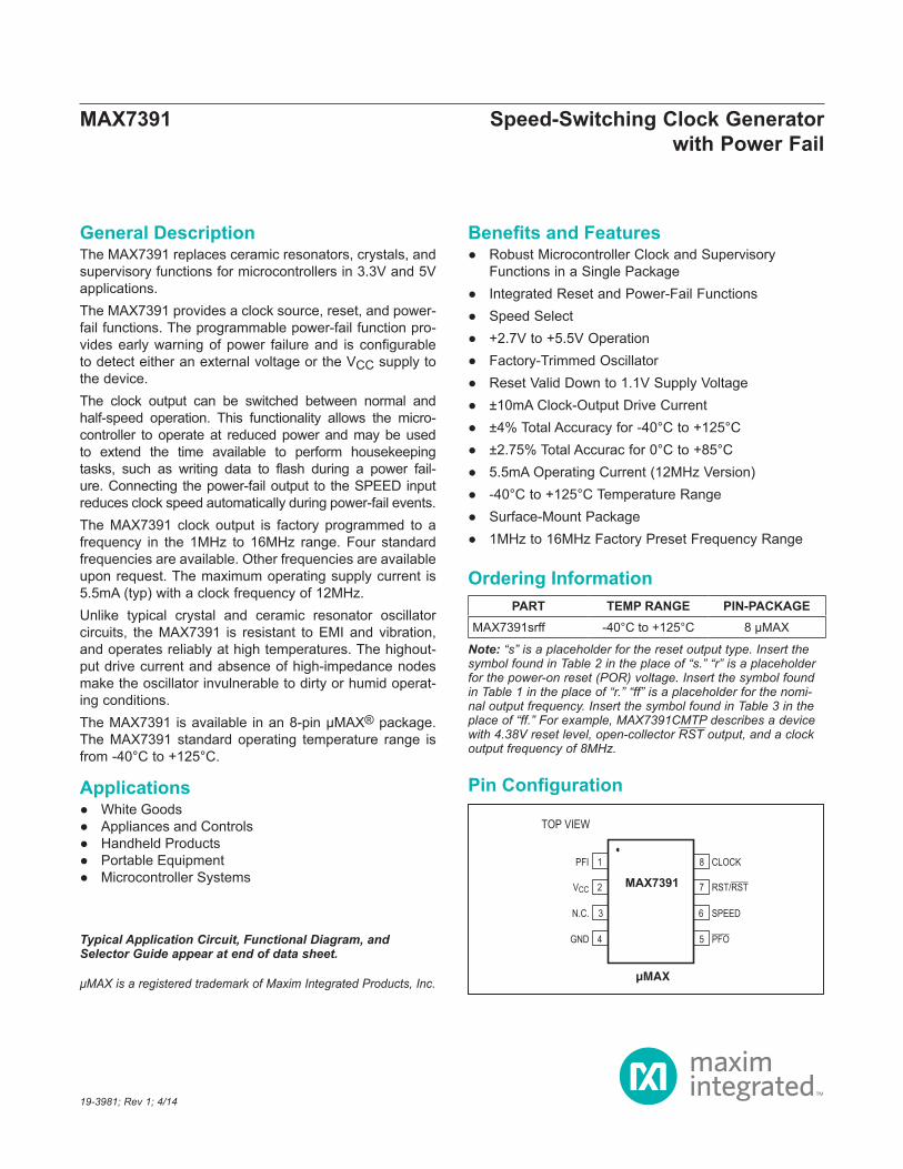
Note: “s” is a placeholder for the reset output type. Insert the symbol found in Table 2 in the place of “s.” “r” is a placeholder for the power-on reset (POR) voltage. Insert the symbol found in Table 1 in the place of “r.” “ff” is a placeholder for the nomi-nal output frequency. Insert the symbol found in Table 3 in the place of “ff.” For example, MAX7391CMTP describes a device with 4.38V reset level, open-collector RST output, and a clock output frequency of 8MHz.
PART TEMP RANGE PIN-PACKAGEMAX7391srff -40°C to +125°C 8 µMAX
SPEED
PFOGND
1
2
8
7
CLOCK
RST/RSTVCC
N.C.
PFI
TOP VIEW
µMAX
3
4
6
5
MAX7391
MAX7391 Speed-Switching Clock Generatorwith Power Fail
Pin Configuration
Ordering Information
VCC to GND...........................................................-0.3V to +6.0VAll Other Pins to GND ................................-0.3V to (VCC + 0.3V)CLOCK, RST/RST, PFO Output Current ..........................±50mAContinuous Power Dissipation
8-Pin μMAX (derate 4.5mW/°C over TA = +70°C).......362mW
Operating Temperature Range .........................-40°C to +125°CJunction Temperature......................................................+150°CStorage Temperature Range .............................-65°C to +150°CLead Temperature (soldering, 10s) .................................+300°C
(Typical Application Circuit, VCC = +2.7V to +5.5V, TA = -40°C to +125°C, 1MHz to 16MHz output frequency range, typical values at VCC = +5.0V, TA = +25°C, unless otherwise noted.) (Note 1)
PARAMETER SYMBOL CONDITIONS MIN TYP MAX UNITSPOWER REQUIREMENTSOperating Supply Voltage VCC 2.7 5.5 V
Valid RST/RST Supply Voltage VCCRMinimum supply voltage for valid RST/RST output, TA = 0°C to +85°C 1.1 V
Operating Supply Current ICCfCLOCK = 12MHz 5.5
mAfCLOCK = 8MHz 4.5
LOGIC INPUT: SPEEDInput Leakage Current ILEAK Input is high 0.5 µA
Logic-Input High Voltage VIH0.7 x VCC
V
Logic-Input Low Voltage VIL0.3 x VCC
V
PUSH-PULL LOGIC OUTPUTS: RST/RST
Output High VOH ISOURCE = 1mA VCC - 1.5 V
Output Low VOL ISINK = 3mA 0.05 0.4 V
OPEN-DRAIN LOGIC OUTPUTS: RST, PFOOutput Low VOLO ISINK = 3mA 0.05 0.4 V
OUTPUT: CLOCK
CLOCK Output High Voltage VOHC ISOURCE = 5mA VCC - 0.3 V
CLOCK Output Low Voltage VOLC ISINK = 5mA 0.3 V
CLOCK Accuracy fCLOCK Table 3, VCC = +5.0V -4 +4 %
MAX7391 Speed-Switching Clock Generatorwith Power Fail
www.maximintegrated.com Maxim Integrated │ 2
Absolute Maximum Ratings
Stresses beyond those listed under “Absolute Maximum Ratings” may cause permanent damage to the device. These are stress ratings only, and functional operation of the device at these or any other conditions beyond those indicated in the operational sections of the specifications is not implied. Exposure to absolute maximum rating conditions for extended periods may affect device reliability.
Electrical Characteristics
(Typical Application Circuit, VCC = +2.7V to +5.5V, TA = -40°C to +125°C, 1MHz to 16MHz output frequency range, typical values at VCC = +5.0V, TA = +25°C, unless otherwise noted.) (Note 1)
Note 1: All parameters are tested at TA = +25°C. Specifications over temperature are guaranteed by design.Note 2: Guaranteed by design. Not production tested.
PARAMETER SYMBOL CONDITIONS MIN TYP MAX UNITSClock Frequency Temperature Coefficient VCC = +5.0V (Note 2) 140 400 ppm/°C
Clock Frequency Supply Voltage Coefficient TA = +25°C (Note 2) 0.67 1 %/V
CLOCK Duty Cycle (Note 2) 45 50 55 %
CLOCK Output Jitter Observation for 20s using a 500MHz oscilloscope 310 ps
RMS
Output Rise Time tRCLOAD = 10pF, 10% to 90% of full scale (Note 2) 2.5 7.0 ns
Output Fall Time tFCLOAD = 10pF, 90% to 10% of full scale (Note 2) 2.5 7.5 ns
INTERNAL POWER-ON RESET
Reset VoltageVTH+ VCC rising, Table 1
TA = +25°C VTH- 1.5%
VTH+ 1.5%
VTA = -40°C to +125°C VTH- 2.5%
VTH+ 2.5%
VTH- VCC falling 0.98 x VTH+
Reset Timeout Period tRST Figure 1 86 135 250 µs
POWER FAIL
Power-Fail Select Threshold VSEL PFI input 0.65 x VCC
0.85 x VCC
V
VCC Monitoring Threshold(Internal Threshold) VITH VCC rising 4.06 4.38 4.60 V
Internal Threshold Hysteresis VIHYST VCC falling 1.0 2 4.0 %VITH
PFI Monitoring Threshold(External Threshold) VETH PFI rising 0.9 1.1 1.4 V
External Threshold Hysteresis VEHYST PFI falling 1.0 3.5 8.0 %VETH
MAX7391 Speed-Switching Clock Generatorwith Power Fail
www.maximintegrated.com Maxim Integrated │ 3
Electrical Characteristics (continued)
(Typical Application Circuit, VCC = +5V, fCLOCK = 16MHz, TA = +25°C, unless otherwise noted.)
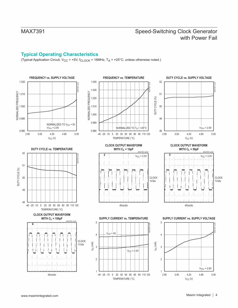
FREQUENCY vs. TEMPERATURE
MAX
7391
toc0
2
TEMPERATURE (°C)
NORM
ALIZ
ED F
REQU
ENCY
1109580655035205-10-25
0.990
1.000
1.010
1.020
1.030
1.040
0.980-40 125
NORMALIZED TO TA = +25°C
DUTY CYCLE vs. SUPPLY VOLTAGE
MAX
7391
toc0
3
VCC (V)
DUTY
CYC
LE (%
)
4.854.203.55
49
50
51
52
482.90 5.50
VTH+ = 2.9V
DUTY CYCLE vs. TEMPERATURE
MAX
7391
toc0
4
DUTY
CYC
LE (%
)
49
50
51
52
48
TEMPERATURE (°C)1109580655035205-10-25-40 125
CLOCK OUTPUT WAVEFORMWITH CL = 10pF
MAX7391 toc05
40ns/div
CLOCK1V/div
VCC = 3.3V
CLOCK OUTPUT WAVEFORMWITH CL = 50pF
MAX7391 toc06
40ns/div
CLOCK1V/div
VCC = 3.3V
CLOCK OUTPUT WAVEFORMWITH CL = 100pF
MAX7391 toc07
40ns/div
CLOCK1V/div
FREQUENCY vs. SUPPLY VOLTAGEM
AX73
91 to
c01
VCC (V)
NORM
ALIZ
ED F
REQU
ENCY
4.854.203.55
0.990
1.000
1.010
1.020
0.9802.90 5.50
NORMALIZED TO VCC = 5VVTH+ = 2.9V
SUPPLY CURRENT vs. TEMPERATURE
MAX
7391
toc0
8
I CC
(mA)
2
3
4
5
1
TEMPERATURE (°C)1109580655035205-10-25-40 125
VCC = 5V
VCC = 3.3V
SUPPLY CURRENT vs. SUPPLY VOLTAGEM
AX73
91 to
c09
VCC (V)
I CC
(mA)
4.854.203.55
2
3
4
5
12.90 5.50
VTH+ = 2.9V
MAX7391 Speed-Switching Clock Generatorwith Power Fail
Maxim Integrated │ 4www.maximintegrated.com
Typical Operating Characteristics
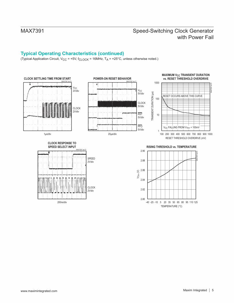
(Typical Application Circuit, VCC = +5V, fCLOCK = 16MHz, TA = +25°C, unless otherwise noted.)
CLOCK SETTLING TIME FROM STARTMAX7391 toc10
1µs/div
CLOCK2V/div
VCC2V/div
POWER-ON RESET BEHAVIORMAX7391 toc11
20µs/div
CLOCK5V/div
VCC5V/div
RST5V/div
PFO5V/div
MAXIMUM VCC TRANSIENT DURATIONvs. RESET THRESHOLD OVERDRIVE
MAX
7391
toc1
2
RESET THRESHOLD OVERDRIVE (mV)
TRAN
SIEN
T DU
RATI
ON (µ
s)
900800700600500400300200
10
100
1000
1100 1000
RESET OCCURS ABOVE THIS CURVE
VCC FALLING FROM VTH+ + 100mV
CLOCK RESPONSE TOSPEED SELECT INPUT
MAX7391 toc13
200ns/div
SPEED2V/div
CLOCK2V/div
RISING THRESHOLD vs. TEMPERATURE
MAX
7391
toc1
4
TEMPERATURE (°C)
V TH+
(V)
1109580655035205-10-25
2.82
2.84
2.86
2.88
2.90
2.80-40 125
MAX7391 Speed-Switching Clock Generatorwith Power Fail
Maxim Integrated │ 5www.maximintegrated.com
Typical Operating Characteristics (continued)
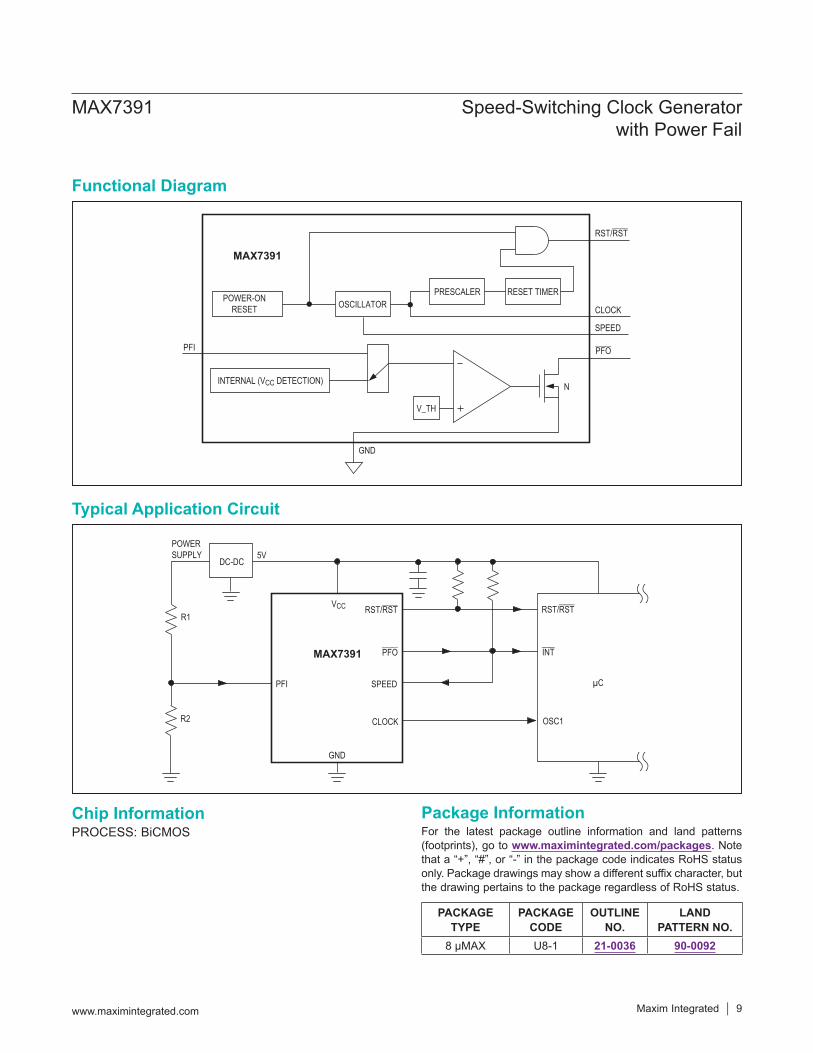
Detailed DescriptionThe MAX7391 replaces ceramic resonators, crystals, and supervisory functions for microcontrollers in 3.3V and 5V applications.The MAX7391 provides a clock source, reset, and power-fail functions. The power-fail output provides early warning of power failure. The power-fail threshold is con-figurable to detect either an external voltage or the VCC supply voltage to the device.The clock output can be switched between normal and half-speed operation. This functionality allows the microcontroller to operate at reduced power and may be used to extend the time available to perform housekeep-ing tasks, such as writing data to flash, during a power failure. Connecting the power-fail output (PFO) to the SPEED input reduces clock speed automatically during power-fail events.The integrated reset provides the power-supply monitor-ing functions necessary to ensure correct microcontroller operation. The reset circuit has built-in power-supply transient immunity and provides both power-on reset and power-fail or brownout reset functionality. Two standard factory-trimmed reset levels are available.A power-fail function is provided for power-supply voltage monitoring and can provide advance notice of an impend-ing power failure. The power-fail input monitors external power-supply voltages through an external resistive divider. Connect PFI to VCC to monitor VCC.
Clock Output (CLOCK)The push-pull clock output (CLOCK) drives a groundcon-nected 1kΩ load or a positive supply connected 500Ω load to within 300mV of either supply rail. CLOCK remains stable over the full operating voltage range and does not generate short output cycles during either power-on or power-off. A typical startup characteristic is shown in the Typical Operating Characteristics section.The clock output frequency is reduced by a factor of two by taking SPEED low. This functionality allows the micro-controller to operate at reduced power and may be used to extend the time available to perform housekeeping tasks, such as writing data to flash during power failure.
ResetThe reset function drives the microcontroller reset input to prevent operation in the cases of the initial power-on set-ting, low power-supply voltages, and the failed watchdog operations. Three reset output versions are available: push-pull RST, push-pull RST, and open-drain RST. The reset timeout period (tRST) is nominally 135s.
Power-On Reset (POR)The internal power-on reset (POR) circuit detects the power-supply voltage (VCC) level at startup. The POR circuit starts the oscillator when VCC exceeds the reset rising threshold level (VTH+). The reset output remains asserted from the time VCC crosses the VTH+ and continues to be asserted for the reset timeout period (tRST). Upon completion of the reset timeout, the reset output is released. See Figure 1.
PIN NAME FUNCTION
1 PFI Power-Fail Input. PFI monitors the condition of either an external supplied voltage or VCC. See the Power Fail section for more details.
2 VCCPower Input. Connect VCC to the power supply. Bypass VCC to GND with a 0.1µF capacitor. Install the bypass capacitor as close to the device as possible.
3 N.C. No Connection
4 GND Ground
5 PFO Power-Fail Output. Open-drain output asserts when the voltage being monitored drops below the power-fail threshold voltage.
6 SPEED Clock-Speed Select Input. Connect SPEED high for the factory-trimmed clock output frequency. Connect SPEED low to reduce the clock output frequency by half.
7 RST/RST
Reset Output. Reset output is available in one of three configurations: push-pull RST, push-pull RST,or open-drain RST. The reset output occurs if any combination of the following conditions occurs: reset output is asserted during power-up, and whenever VCC is below the reset threshold level; for devices with WDI, reset output asserts when WDI does not receive a rising or falling edge within the watchdog timeout period.
8 CLOCK Clock Output
MAX7391 Speed-Switching Clock Generatorwith Power Fail
www.maximintegrated.com Maxim Integrated │ 6
Pin Description
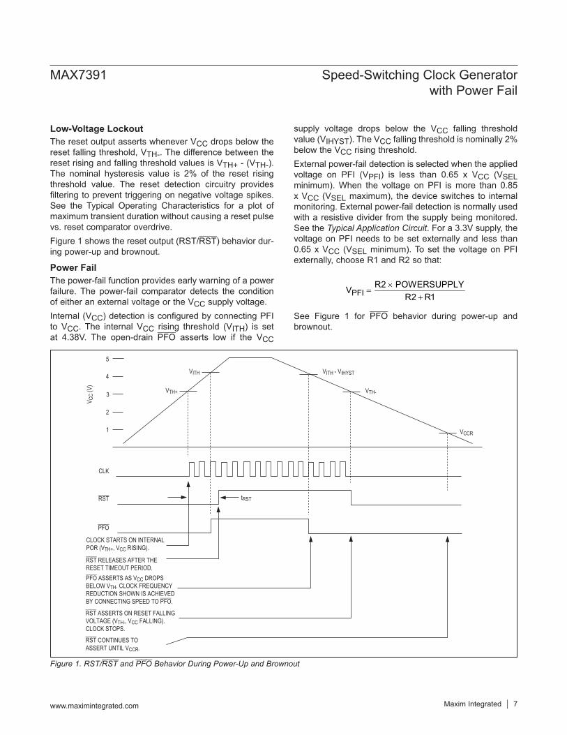
Low-Voltage LockoutThe reset output asserts whenever VCC drops below the reset falling threshold, VTH-. The difference between the reset rising and falling threshold values is VTH+ - (VTH-). The nominal hysteresis value is 2% of the reset rising threshold value. The reset detection circuitry provides filtering to prevent triggering on negative voltage spikes. See the Typical Operating Characteristics for a plot of maximum transient duration without causing a reset pulse vs. reset comparator overdrive.Figure 1 shows the reset output (RST/RST) behavior dur-ing power-up and brownout.
Power FailThe power-fail function provides early warning of a power failure. The power-fail comparator detects the condition of either an external voltage or the VCC supply voltage.Internal (VCC) detection is configured by connecting PFI to VCC. The internal VCC rising threshold (VITH) is set at 4.38V. The open-drain PFO asserts low if the VCC
supply voltage drops below the VCC falling threshold value (VIHYST). The VCC falling threshold is nominally 2% below the VCC rising threshold.External power-fail detection is selected when the applied voltage on PFI (VPFI) is less than 0.65 x VCC (VSEL minimum). When the voltage on PFI is more than 0.85 x VCC (VSEL maximum), the device switches to internal monitoring. External power-fail detection is normally used with a resistive divider from the supply being monitored. See the Typical Application Circuit. For a 3.3V supply, the voltage on PFI needs to be set externally and less than 0.65 x VCC (VSEL minimum). To set the voltage on PFI externally, choose R1 and R2 so that:
PFIR2 POWERSUPPLYV
R2 R1×
=+
See Figure 1 for PFO behavior during power-up and brownout.
Figure 1. RST/RST and PFO Behavior During Power-Up and Brownout
5
4
3
2
1
CLK
tRST
VTH+
VITH
VTH-
VCCR
VITH - VIHYST
RST
PFO
CLOCK STARTS ON INTERNALPOR (VTH+, VCC RISING).
RST RELEASES AFTER THERESET TIMEOUT PERIOD.
V CC
(V)
PFO ASSERTS AS VCC DROPSBELOW VTH. CLOCK FREQUENCYREDUCTION SHOWN IS ACHIEVEDBY CONNECTING SPEED TO PFO.
RST CONTINUES TOASSERT UNTIL VCCR.
RST ASSERTS ON RESET FALLINGVOLTAGE (VTH-, VCC FALLING). CLOCK STOPS.
MAX7391 Speed-Switching Clock Generatorwith Power Fail
www.maximintegrated.com Maxim Integrated │ 7
Applications InformationInterfacing to a Microcontroller Clock InputThe clock output is a push-pull, CMOS logic output, which directly drives any microprocessor (μP) or microcontroller (μC) clock input. There are no impedancematching issues when using the MAX7391. Operate the MAX7391 and μC (or other clock input device) from the same supply voltage level. Refer to the microcontroller data sheet for clock-input compatibility with external clock signals. Table 3 lists clock output frequency.The MAX7391 requires no biasing components or load capacitance. When using the MAX7391 to retrofit a crys-tal oscillator, remove all biasing components from the oscillator input.
Power-Supply ConsiderationsThe MAX7391 operates with power-supply voltages in the 2.7V to 5.5V range. Good power-supply decoupling is needed to maintain the power-supply rejection per-formance of the MAX7391. Bypass VCC to GND with a 0.1μF surface-mount ceramic capacitor. Mount the bypass capacitor as close to the device as possible. If possible, mount the MAX7391 close to the microcon-troller’s decoupling capacitor so that additional decou-pling is not required.A larger-value bypass capacitor is recommended if the MAX7391 is to operate with a large capacitive load. Use a bypass capacitor value of at least 1000 times that of the output load capacitance.
Output JitterThe MAX7391’s jitter performance is given in the Electrical Characteristics table as a peak-to-peak value obtained by observing the output of the device for 20s with a 500MHz oscilloscope. Jitter measurements are approximately proportional to the period of the output frequency of the device. Thus, a 4MHz part has approximately twice the jitter value of an 8MHz part.The jitter performance of all clock sources degrades in the presence of mechanical and electrical interference. The MAX7391 is immune to vibration, shock, and EMI influences, and thus provides a considerably more robust clock source than crystal- or ceramic-resonatorbased oscillator circuits.
Note: Other versions with different features are available. Refer to the MAX7387/MAX7388 and MAX7389/MAX7390 data sheets.
Note: Standard values are shown in bold. Contact factory for other POR voltages.
Note: Standard values are shown in bold. Contact factory for other POR voltages. Note: Contact factory for other frequencies.
Table 1. POR Voltage
Table 2. Reset Output Type Table 3. Clock Output Frequency
PARTFREQUENCY RANGE
(MHz)
RESET FUNCTION
WATCHDOG INPUT (WDI) / WATCHDOG
OUTPUT (WDO)
POWER-FAIL INPUT (PFI)/POWER-FAIL
OUTPUT (PFO)SPEED PIN-
PACKAGE
MAX7387 1 to 32 Yes Yes/yes Yes/yes — 10 µMAX
MAX7388 1 to 32 Yes Yes/no No/yes — 8 µMAX
MAX7389 1 to 32 Yes Yes/yes — — 8 µMAX
MAX7390 1 to 32 Yes Yes/no — Yes 8 µMAX
MAX7391 1 to 32 Yes — Yes/yes Yes 8 µMAX
POWER-ON RESET VOLTAGE (VTH) r4.38 M3.96 J
3.44 N
3.34 P
3.13 Q
2.89 S2.82 V
2.5 X
OUTPUT TYPE sPush-pull RST A
Push-pull RST B
Open collector RST C
CLOCK FREQUENCY (fCLOCK) (MHz) ff4 RD
8 TP
12 VB
16 WB
MAX7391 Speed-Switching Clock Generatorwith Power Fail
www.maximintegrated.com Maxim Integrated │ 8
Selector Guide
PACKAGE TYPE
PACKAGE CODE
OUTLINE NO.
LAND PATTERN NO.
8 µMAX U8-1 21-0036 90-0092
RST/RSTVCC
GND
PFO
R1
POWERSUPPLY 5V
R2
PFI SPEED
CLOCK
INT
RST/RST
µC
OSC1
DC-DC
MAX7391
RESET TIMER
RST/RST
CLOCK
SPEED
PFI PFO
PRESCALER
INTERNAL (VCC DETECTION)
OSCILLATOR
V_TH
GND
POWER-ONRESET
N
MAX7391
MAX7391 Speed-Switching Clock Generatorwith Power Fail
www.maximintegrated.com Maxim Integrated │ 9
Typical Application Circuit
Functional Diagram
Chip InformationPROCESS: BiCMOS
Package InformationFor the latest package outline information and land patterns (footprints), go to www.maximintegrated.com/packages. Note that a “+”, “#”, or “-” in the package code indicates RoHS status only. Package drawings may show a different suffix character, but the drawing pertains to the package regardless of RoHS status.
REVISIONNUMBER
REVISION DATE DESCRIPTION PAGES
CHANGED
0 1/06 Initial release —
1 4/14 No /V OPNs; removed Automotive reference from Applications section 1
Maxim Integrated cannot assume responsibility for use of any circuitry other than circuitry entirely embodied in a Maxim Integrated product. No circuit patent licenses are implied. Maxim Integrated reserves the right to change the circuitry and specifications without notice at any time. The parametric values (min and max limits) shown in the Electrical Characteristics table are guaranteed. Other parametric values quoted in this data sheet are provided for guidance.
Maxim Integrated and the Maxim Integrated logo are trademarks of Maxim Integrated Products, Inc.
MAX7391 Speed-Switching Clock Generatorwith Power Fail
© 2014 Maxim Integrated Products, Inc. │ 10
Revision History
For pricing, delivery, and ordering information, please contact Maxim Direct at 1-888-629-4642, or visit Maxim Integrated’s website at www.maximintegrated.com.