mc56f8025, 56f8035 / 56f8025 technical data - data...
TRANSCRIPT

56F800016-bit Digital Signal Controllers
freescale.com
56F8035/56F8025 Data SheetTechnical Data
MC56F8025Rev. 6 02/2010

56F8035/56F8025 Data Sheet, Rev. 6
2 Freescale Semiconductor
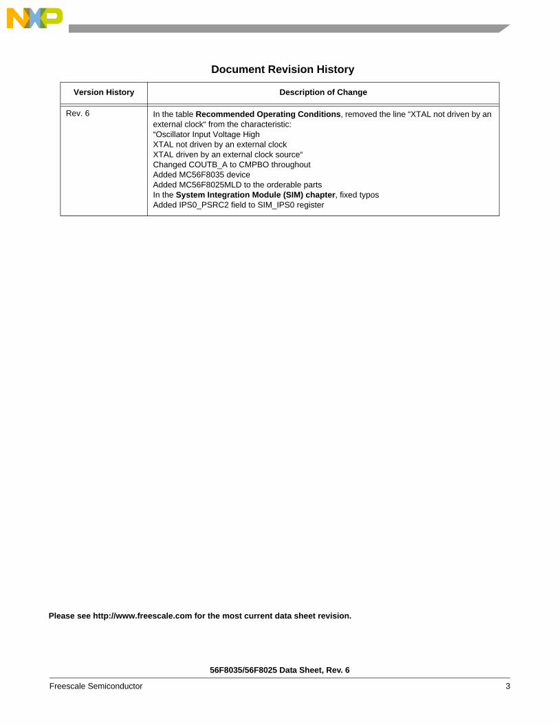
Document Revision History
Version History Description of Change
Rev. 0 Initial public release.
Rev. 1 • In Table 5-3, changed the ITCN_BASE address from $00 F060 (incorrect value) to $00 F0E0 (the correct value).
• In Table 10-4, added an entry for flash data retention with less than 100 program/erase cycles (minimum 20 years).
• In Table 10-6, changed the device clock speed in STOP mode from 8MHz to 4MHz.• In Table 10-12, changed the typical relaxation oscillator output frequency in Standby mode
from 400kHz to 200kHz.• Changed input propagation delay values in Table 10-20 as follows:
Old values: 1 μs typical, 2 μs maximumNew values: 35 ns typical, 45 ns maximum
Rev. 2 • In Table 10-19, changed the maximum ADC internal clock frequency from 8MHz to 5.33MHz.
• Replaced the case outline schematics in Figure 11-2, Figure 11-3, and Figure 11-4.
Rev. 3 Added the following note to the description of the TMS signal in Table 2-3:Note: Always tie the TMS pin to VDD through a 2.2K resistor.
Rev. 4 • Changed the VBA register reset value and updated the footnote in Section 5.6.8.• Changed the STANDBY > STOP IDD values in Table 10-6 as follows:
Typical: was 290μA, is 540μAMaximum: was 390μA, is 650μA
• Changed the POWERDOWN IDD values in Table 10-6 as follows:
Typical: was 190μA, is 440μAMaximum: was 250μA, is 550μA
• Changed footnote 1 in Table 10-12 (was “Output frequency after application of 8MHz trim value, at 125°C.”, is “Output frequency after application of factory trim”).
• Deleted the text “at 125°C” from Figure 10-5.• Changed the maximum input offset voltage in Table 10-20 (was +/- 20 mV, is ±35 mV).
Rev. 5 • In Table 2-3, change VCAP value from 4.7μF to 2.2μF.
• Revised Section 7, Security Features.• Fixed miscellaneous typos.
56F8035/56F8025 Data Sheet, Rev. 6
Freescale Semiconductor 3
Rev. 6 In the table Recommended Operating Conditions, removed the line “XTAL not driven by an external clock“ from the characteristic:“Oscillator Input Voltage HighXTAL not driven by an external clockXTAL driven by an external clock source“Changed COUTB_A to CMPBO throughoutAdded MC56F8035 deviceAdded MC56F8025MLD to the orderable partsIn the System Integration Module (SIM) chapter, fixed typosAdded IPS0_PSRC2 field to SIM_IPS0 register
Document Revision History
Version History Description of Change
Please see http://www.freescale.com for the most current data sheet revision.

56F8035/56F8025 Data Sheet, Rev. 6
4 Freescale Semiconductor
56F8035/56F8025 Block Diagram
ProgrammableIntervalTimer
Program Controllerand Hardware Looping Unit
Data ALU16 x 16 + 36 -> 36-Bit MAC
Three 16-bit Input RegistersFour 36-bit Accumulators
Address Generation Unit
Bit Manipulation
Unit
16-Bit56800E Core
InterruptController
4
Unified Data / Program RAM
2K x 164K x 16
PDB
PDB
XAB1XAB2
XDB2
CDBR
QSPIor PWMor I2C
or TMRAor GPIOB
IPBus Bridge (IPBB)
System BusControl
R/W ControlMemory
PAB
PAB
CDBW
CDBRCDBW
JTAG/EOnCE Port or GPIOD
Digital Reg Analog Reg
Low-VoltageSupervisor
VCAP VDD VSS VDDA VSSA4
RESET or GPIOA
AD04
ClockGenerator*
SystemIntegration
Module
POR O
SC
PWMor TMRA or CMP
or GPIOA
*Includes On-Chip Relaxation Oscillator
COP/Watchdog
AD14
Program Memory16K x 16 Flash32K x 16 Flash
ADCor CMP
or GPIOC
QSCI or PWMor I2C
or TMRA or GPIOB
3
3
I2Cor CMP
or GPIOB
2
2
XTAL, CLKIN, or GPIOD
EXTAL or GPIOD
2
11
DAC
• Up to 32 MIPS at 32MHz core frequency• DSP and MCU functionality in a unified,
C-efficient architecture• 56F8035 offers 64KB (32K x 16) Program Flash• 56F8025 offers 32KB (16K x 16) Program Flash• 56F8035 offers 8KB (4K x 16) Unified Data/Program
RAM• 56F8025 offers 4KB (2K x 16) Unified Data/Program
RAM• One 6-channel PWM module• Two 4-channel 12-bit Analog-to-Digital Converters
(ADCs)• Two Internal 12-bit Digital-to-Analog Converters
(DACs)
• Two Analog Comparators• Three Programmable Interval Timers (PITs)• One Queued Serial Communication Interface (QSCI)
with LIN slave functionality• One Queued Serial Peripheral Interfaces (QSPI)• One 16-bit Quad Timer
• One Inter-Integrated Circuit (I2C) port• Computer Operating Properly (COP)/Watchdog• On-Chip Relaxation Oscillator• Integrated Power-On Reset (POR) and Low-Voltage
Interrupt (LVI) module• JTAG/Enhanced On-Chip Emulation (OnCE™) for
unobtrusive, real-time debugging• Up to 35 GPIO lines
56F8035/56F8025 General Description

56F8035/56F8025 Data Sheet, Rev. 6
Freescale Semiconductor 5
Part 1 Overview. . . . . . . . . . . . . . . . . . . . . . . . 61.1 56F8035/56F8025 Features . . . . . . . . . . . 61.2 56F8035/56F8025 Description . . . . . . . . . 81.3 Award-Winning Development
Environment . . . . . . . . . . . . . . . . . . . 91.4 Architecture Block Diagram . . . . . . . . . . . 91.5 Product Documentation . . . . . . . . . . . . . 171.6 Data Sheet Conventions . . . . . . . . . . . . . 17
Part 2 Signal/Connection Descriptions . . . 182.1 Introduction . . . . . . . . . . . . . . . . . . . . . . . 182.2 56F8035/56F8025 Signal Pins . . . . . . . . 22
Part 3 OCCS . . . . . . . . . . . . . . . . . . . . . . . . . 333.1 Overview. . . . . . . . . . . . . . . . . . . . . . . . . 333.2 Features . . . . . . . . . . . . . . . . . . . . . . . . . 333.3 Operating Modes . . . . . . . . . . . . . . . . . . 333.4 Internal Clock Source . . . . . . . . . . . . . . . 343.5 Crystal Oscillator. . . . . . . . . . . . . . . . . . . 343.6 Ceramic Resonator . . . . . . . . . . . . . . . . . 353.7 External Clock Input - Crystal Oscillator
Option. . . . . . . . . . . . . . . . . . . . . . . 353.8 Alternate External Clock Input . . . . . . . . 36
Part 4 Memory Maps. . . . . . . . . . . . . . . . . . . 364.1 Introduction . . . . . . . . . . . . . . . . . . . . . . . 364.2 Interrupt Vector Table . . . . . . . . . . . . . . . 374.3 Program Map . . . . . . . . . . . . . . . . . . . . . 394.4 Data Map . . . . . . . . . . . . . . . . . . . . . . . . 394.5 EOnCE Memory Map . . . . . . . . . . . . . . . 414.6 Peripheral Memory-Mapped Registers . . 42
Part 5 Interrupt Controller (ITCN) . . . . . . . . 565.1 Introduction . . . . . . . . . . . . . . . . . . . . . . . 565.2 Features . . . . . . . . . . . . . . . . . . . . . . . . . 565.3 Functional Description . . . . . . . . . . . . . . 565.4 Block Diagram. . . . . . . . . . . . . . . . . . . . . 595.5 Operating Modes . . . . . . . . . . . . . . . . . . 595.6 Register Descriptions . . . . . . . . . . . . . . . 595.7 Resets. . . . . . . . . . . . . . . . . . . . . . . . . . . 78
Part 6 System Integration Module (SIM) . . . 796.1 Introduction . . . . . . . . . . . . . . . . . . . . . . . 796.2 Features . . . . . . . . . . . . . . . . . . . . . . . . . 806.3 Register Descriptions . . . . . . . . . . . . . . . 816.4 Clock Generation Overview . . . . . . . . . 1066.5 Power-Saving Modes . . . . . . . . . . . . . . 1086.6 Resets. . . . . . . . . . . . . . . . . . . . . . . . . . 1096.7 Clocks . . . . . . . . . . . . . . . . . . . . . . . . . . 1106.8 Interrupts. . . . . . . . . . . . . . . . . . . . . . . . 112
Part 7 Security Features. . . . . . . . . . . . . . . 1127.1 Operation with Security Enabled. . . . . . 1127.2 Flash Access Lock and Unlock
Mechanisms . . . . . . . . . . . . . . . . . 113
7.3 Product Analysis. . . . . . . . . . . . . . . . . . 114
Part 8 General-Purpose Input/Output (GPIO) . . . . . . . . . . . . . . . . . . . . . . . .114
8.1 Introduction. . . . . . . . . . . . . . . . . . . . . . 1148.2 Configuration . . . . . . . . . . . . . . . . . . . . 1148.3 Reset Values . . . . . . . . . . . . . . . . . . . . 117
Part 9 Joint Test Action Group (JTAG) . . .1229.1 56F8035/56F8025 Information . . . . . . . 122
Part 10Specifications. . . . . . . . . . . . . . . . . .12210.1 General Characteristics . . . . . . . . . . . . 12210.2 DC Electrical Characteristics . . . . . . . . 12610.3 AC Electrical Characteristics . . . . . . . . 12910.4 Flash Memory Characteristics . . . . . . . 13010.5 External Clock Operation Timing . . . . . 13010.6 Phase Locked Loop Timing . . . . . . . . . 13110.7 Relaxation Oscillator Timing. . . . . . . . . 13210.8 Reset, Stop, Wait, Mode Select, and
Interrupt Timing . . . . . . . . . . . . . . 13310.9 Serial Peripheral Interface (SPI)
Timing . . . . . . . . . . . . . . . . . . . . . 13410.10 Quad Timer Timing. . . . . . . . . . . . . . . . 13810.11 Serial Communication Interface (SCI)
Timing . . . . . . . . . . . . . . . . . . . . . 14010.12 Inter-Integrated Circuit Interface (I2C)
Timing . . . . . . . . . . . . . . . . . . . . . 14110.13 JTAG Timing. . . . . . . . . . . . . . . . . . . . . 14310.14 Analog-to-Digital Converter (ADC)
Parameters . . . . . . . . . . . . . . . . . 14410.15 Equivalent Circuit for ADC Inputs . . . . . 14510.16 Comparator (CMP) Parameters . . . . . . 14610.17 Digital-to-Analog Converter (DAC)
Parameters . . . . . . . . . . . . . . . . . 14610.18 Power Consumption . . . . . . . . . . . . . . . 148
Part 11Packaging . . . . . . . . . . . . . . . . . . . . .14911.1 56F8035/56F8025 Package and
Pin-Out Information . . . . . . . . . . . 149
Part 12Design Considerations . . . . . . . . . .15512.1 Thermal Design Considerations . . . . . . 15512.2 Electrical Design Considerations . . . . . 156
Part 13Ordering Information . . . . . . . . . . . .157
Part 14Appendix. . . . . . . . . . . . . . . . . . . . . .158
56F8035/56F8025 Data Sheet Table of Contents

56F8035/56F8025 Data Sheet, Rev. 6
6 Freescale Semiconductor
Part 1 Overview
1.1 56F8035/56F8025 Features
1.1.1 Digital Signal Controller Core• Efficient 16-bit 56800E family Digital Signal Controller (DSC) engine with dual Harvard architecture• As many as 32 Million Instructions Per Second (MIPS) at 32MHz core frequency• Single-cycle 16 × 16-bit parallel Multiplier-Accumulator (MAC)• Four 36-bit accumulators, including extension bits• 32-bit arithmetic and logic multi-bit shifter• Parallel instruction set with unique DSP addressing modes• Hardware DO and REP loops• Three internal address buses• Four internal data buses• Instruction set supports both DSP and controller functions• Controller-style addressing modes and instructions for compact code• Efficient C compiler and local variable support• Software subroutine and interrupt stack with depth limited only by memory• JTAG/Enhanced On-Chip Emulation (OnCE) for unobtrusive, processor speed-independent real-time
debugging
1.1.2 Difference Between DevicesTable 1-1 outlines the key differences between the 56F8033 and 56F8023 devices.
1.1.3 Memory• Dual Harvard architecture permits as many as three simultaneous accesses to program and data memory• Flash security and protection that prevent unauthorized users from gaining access to the internal Flash• On-chip memory
— 64KB of Program Flash (56F80235 device)32KB of Program Flash (56F8025 device)
— 8KB of Unified Data/Program RAM (56F8035 device) 4KB of Unified Data/Program RAM (56F8025 device)
• EEPROM emulation capability using Flash
Table 1-1 Device DifferencesOn-Chip Memory 56F8035 56F8025
Program Flash (PFLASH) 64KB 32KB
Unified RAM (RAM) 8KB 4KB

56F8035/56F8025 Features
56F8035/56F8025 Data Sheet, Rev. 6
Freescale Semiconductor 7
1.1.4 Peripheral Circuits for 56F8035/56F8025• One multi-function six-output Pulse Width Modulator (PWM) module
— Up to 96MHz PWM operating clock— 15 bits of resolution— Center-aligned and edge-aligned PWM signal mode— Four programmable fault inputs with programmable digital filter— Double-buffered PWM registers— Each complementary PWM signal pair allows selection of a PWM supply source from:
– PWM generator– External GPIO– Internal timers– Analog comparator outputs– ADC conversion result which compares with values of ADC high- and low-limit registers to set
PWM output• Two independent 12-bit Analog-to-Digital Converters (ADCs)
— 2 x 4 channel inputs— Supports both simultaneous and sequential conversions— ADC conversions can be synchronized by both PWM and timer modules— Sampling rate up to 2.67MSPS— 16-word result buffer registers
• Two internal 12-bit Digital-to-Analog Converters (DACs)— 2 microsecond settling time when output swing from rail to rail— Automatic waveform generation generates square, triangle and sawtooth waveforms with
programmable period, update rate, and range• One 16-bit multi-purpose Quad Timer module (TMR)
— Up to 96MHz operating clock— Eight independent 16-bit counter/timers with cascading capability— Each timer has capture and compare capability— Up to 12 operating modes
• One Queued Serial Communication Interface (QSCI) with LIN Slave functionality— Full-duplex or single-wire operation— Two receiver wake-up methods:
– Idle line – Address mark
— Four-bytes-deep FIFOs are available on both transmitter and receiver• One Queued Serial Peripheral Interfaces (QSPI)

56F8035/56F8025 Data Sheet, Rev. 6
8 Freescale Semiconductor
— Full-duplex operation— Master and slave modes— Four-words-deep FIFOs available on both transmitter and receiver— Programmable Length Transactions (2 to 16 bits)
• One Inter-Integrated Circuit (I2C) port— Operates up to 400kbps— Supports both master and slave operation— Supports both 10-bit address mode and broadcasting mode
• Three 16-bit Programmable Interval Timers (PITs)• Two analog Comparators (CMPs)
— Selectable input source includes external pins, DACs— Programmable output polarity— Output can drive Timer input, PWM fault input, PWM source, external pin output and trigger ADCs— Output falling and rising edge detection able to generate interrupts
• Computer Operating Properly (COP)/Watchdog timer capable of selecting different clock sources• Up to 35 General-Purpose I/O (GPIO) pins with 5V tolerance• Integrated Power-On Reset (POR) and Low-Voltage Interrupt (LVI) module• Phase Lock Loop (PLL) provides a high-speed clock to the core and peripherals• Clock sources:
— On-chip relaxation oscillator— External clock: Crystal oscillator, ceramic resonator, and external clock source
• JTAG/EOnCE debug programming interface for real-time debugging
1.1.5 Energy Information• Fabricated in high-density CMOS with 5V tolerance• On-chip regulators for digital and analog circuitry to lower cost and reduce noise• Wait and Stop modes available• ADC smart power management• Each peripheral can be individually disabled to save power
1.2 56F8035/56F8025 DescriptionThe 56F8035/56F8025 is a member of the 56800E core-based family of Digital Signal Controllers(DSCs). It combines, on a single chip, the processing power of a DSP and the functionality of amicrocontroller with a flexible set of peripherals to create an extremely cost-effective solution. Becauseof its low cost, configuration flexibility, and compact program code, the 56F8035/56F8025 is well-suitedfor many applications. The 56F8035/56F8025 includes many peripherals that are especially useful forindustrial control, motion control, home appliances, general-purpose inverters, smart sensors, fire and

Award-Winning Development Environment
56F8035/56F8025 Data Sheet, Rev. 6
Freescale Semiconductor 9
security systems, switched-mode power supply, power management, and medical monitoringapplications.
The 56800E core is based on a dual Harvard-style architecture consisting of three execution unitsoperating in parallel, allowing as many as six operations per instruction cycle. The MCU-styleprogramming model and optimized instruction set allow straightforward generation of efficient, compactDSP and control code. The instruction set is also highly efficient for C compilers to enable rapiddevelopment of optimized control applications.
The 56F8035/56F8025 supports program execution from internal memories. Two data operands can beaccessed from the on-chip data RAM per instruction cycle. The 56F8035/56F8025 also offers up to 35General-Purpose Input/Output (GPIO) lines, depending on peripheral configuration.
The 56F8035 Digital Signal Controller includes 64KB of Program Flash and 8KB of UnifiedData/Program RAM. The 56F8025 Digital Signal Controller includes 32KB of Program Flash and 4KB ofUnified Data/Program RAM. Program Flash memory can be independently bulk erased or erased in pages.Program Flash page erase size is 512 Bytes (256 Words).
A full set of programmable peripherals — PWM, ADCs, QSCI, QSPI, I2C, PITs, Quad Timers, DACs,and analog comparators — supports various applications. Each peripheral can be independently shut downto save power. Any pin in these peripherals can also be used as General Purpose Input/Outputs (GPIOs).
1.3 Award-Winning Development EnvironmentProcessor ExpertTM (PE) provides a Rapid Application Design (RAD) tool that combines easy-to-usecomponent-based software application creation with an expert knowledge system.
The CodeWarrior Integrated Development Environment is a sophisticated tool for code navigation,compiling, and debugging. A complete set of evaluation modules (EVMs), demonstration board kit anddevelopment system cards will support concurrent engineering. Together, PE, CodeWarrior and EVMscreate a complete, scalable tools solution for easy, fast, and efficient development.
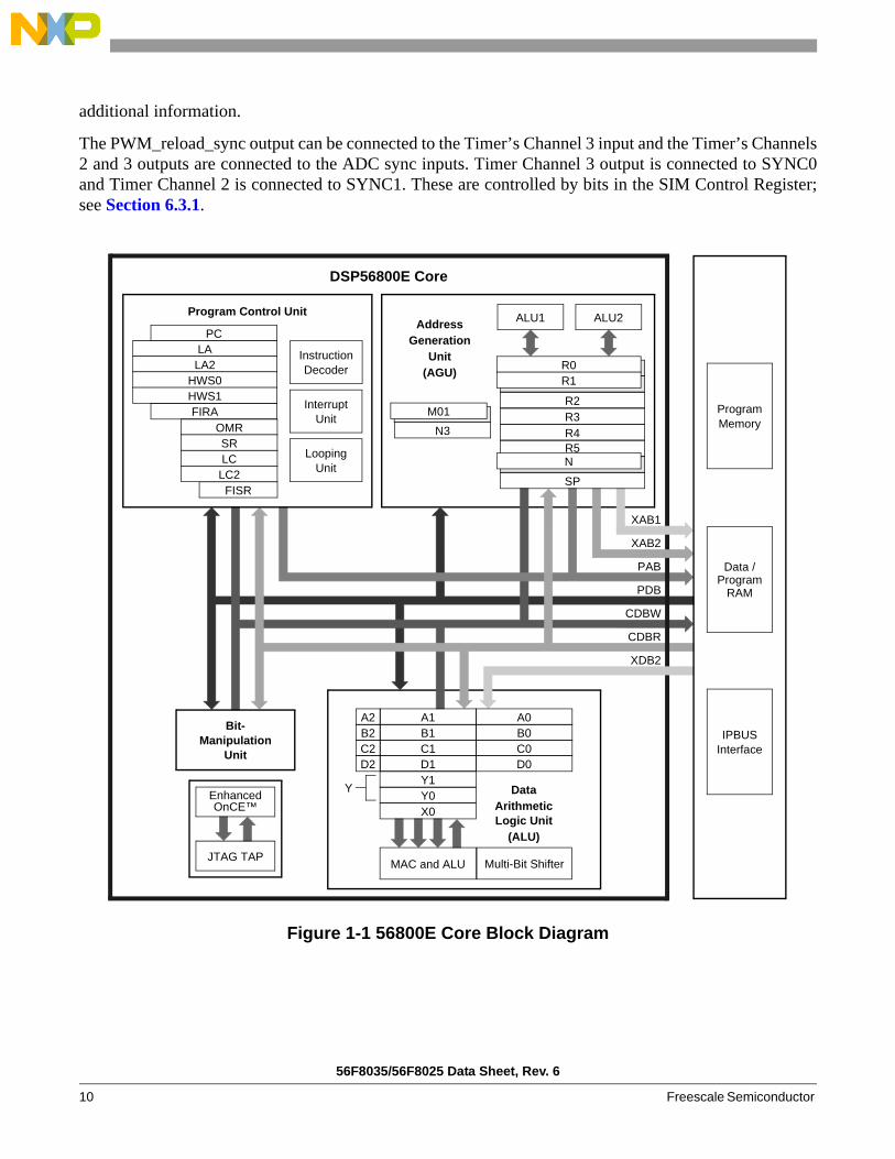
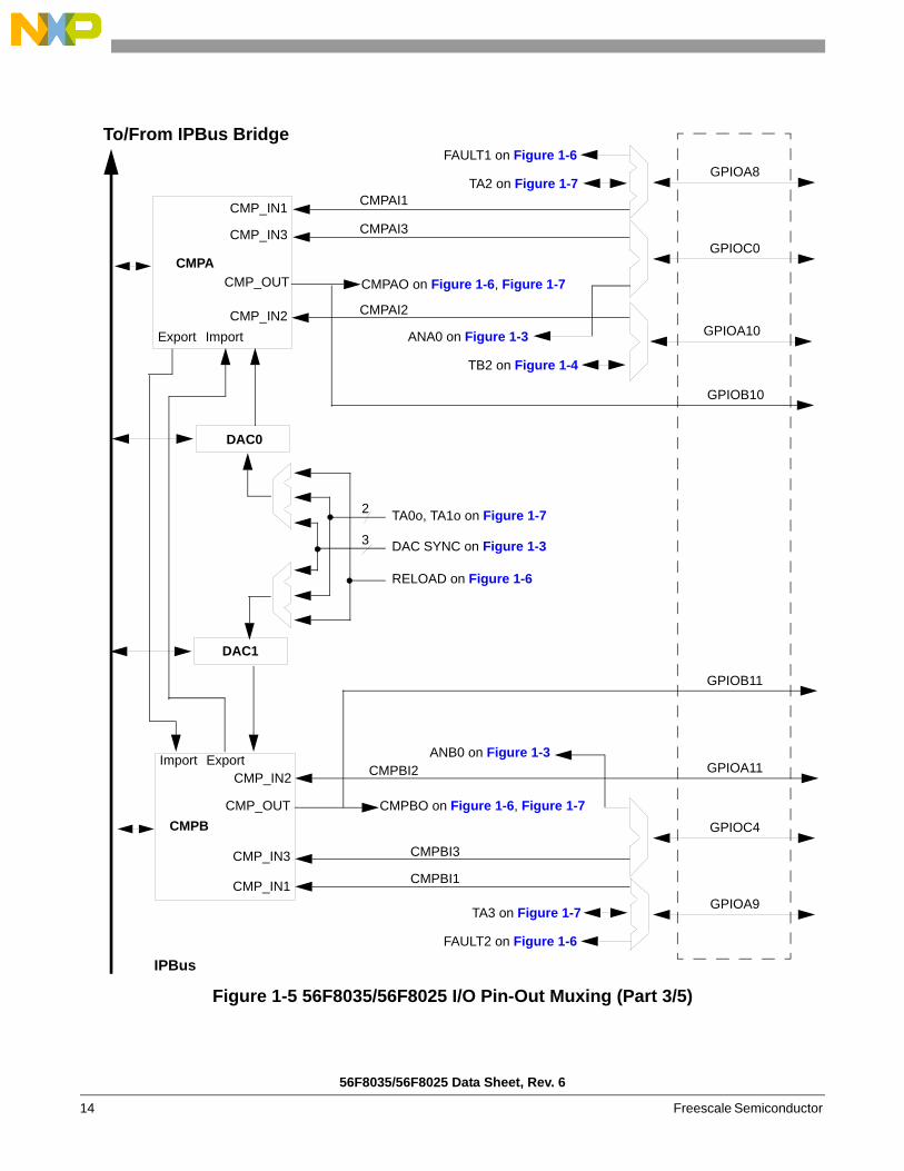
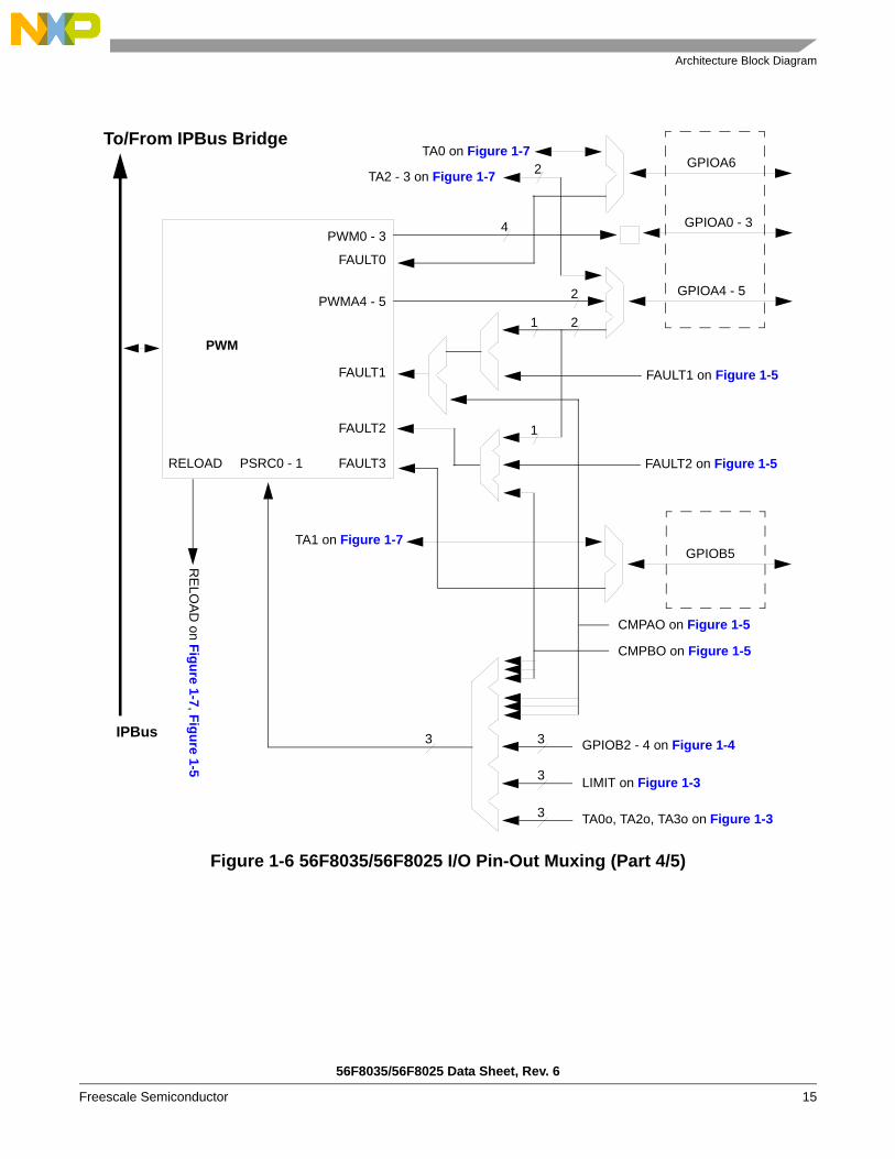
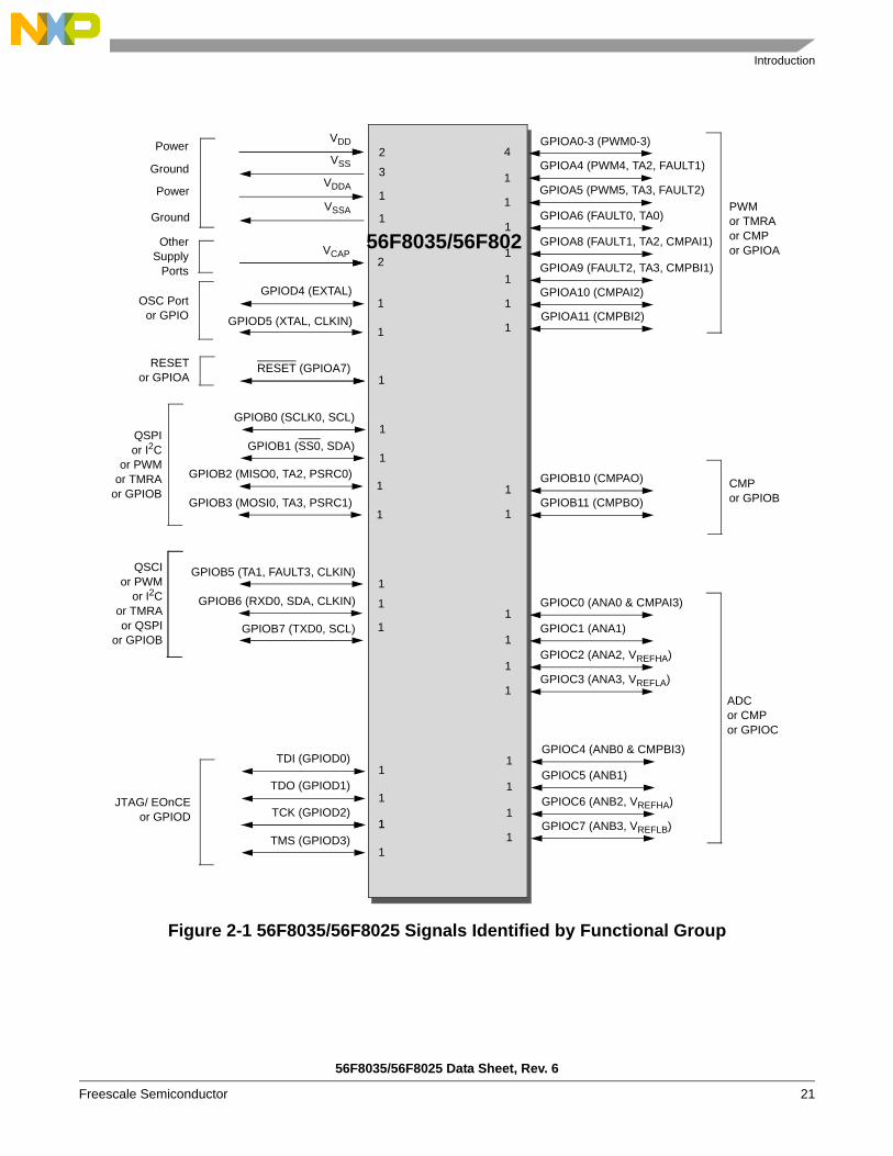
1.4 Architecture Block Diagram The 56F8035/56F8025’s architecture is shown in Figures 1-1, 1-2, 1-3, 1-4, 1-5, 1-6, and 1-7. Figure 1-1illustrates how the 56800E system buses communicate with internal memories and the IPBus Bridge andthe internal connections between each unit of the 56800E core. Figure 1-2 shows the peripherals andcontrol blocks connected to the IPBus Bridge. Figures 1-3, 1-4, 1-5, 1-6, and 1-7 detail how the device’sI/O pins are muxed. The figures do not show the on-board regulator and power and ground signals. Pleasesee Part 2, Signal/Connection Descriptions, for information about which signals are multiplexed withthose of other peripherals.
1.4.1 PWM, TMR and ADC ConnectionsFigure 1-6 shows the over-limit and under-limit connections from the ADC to the PWM and theconnections to the PWM from the TMR and GPIO. These signals can control the PWM outputs in a similarmanner as the PWM generator. See the 56F802x and 56F803x Peripheral Reference Manual for
56F8035/56F8025 Data Sheet, Rev. 6
10 Freescale Semiconductor
additional information.
The PWM_reload_sync output can be connected to the Timer’s Channel 3 input and the Timer’s Channels2 and 3 outputs are connected to the ADC sync inputs. Timer Channel 3 output is connected to SYNC0and Timer Channel 2 is connected to SYNC1. These are controlled by bits in the SIM Control Register;see Section 6.3.1.
Figure 1-1 56800E Core Block Diagram
Data
DSP56800E Core
ArithmeticLogic Unit
(ALU)
XAB2
PAB
PDB
CDBW
CDBR
XDB2
ProgramMemory
Data /
IPBUSInterface
Bit-Manipulation
Unit
N3M01
Address
XAB1
GenerationUnit
(AGU)
PCLA
LA2HWS0HWS1FIRA
OMRSR
FISR
LCLC2
InstructionDecoder
InterruptUnit
LoopingUnit
Program Control Unit ALU1 ALU2
MAC and ALU
A1A2 A0B1B2 B0C1C2 C0D1D2 D0Y1Y0X0
Enhanced
JTAG TAP
R2R3R4R5
SP
R0R1
N
Y
Multi-Bit Shifter
OnCE™
ProgramRAM

Architecture Block Diagram
56F8035/56F8025 Data Sheet, Rev. 6
Freescale Semiconductor 11
Figure 1-2 Peripheral Subsystem
IPBus
GPIO A
Interrupt Controller
To/From IPBus Bridge
GPIO B
GPIO C
OCCS(ROSC / PLL /
OSC)
POR & LVI
SIMGPIO D
Low-Voltage Interrupt
System POR
COP Reset
RESET(Muxed with GPIOA7)
COP
(Continues on Figure 1-3)

56F8035/56F8025 Data Sheet, Rev. 6
12 Freescale Semiconductor
Figure 1-3 56F8035/56F8025 I/O Pin-Out Muxing (Part 1/5)
To/From IPBus Bridge
IPBus
3DAC SYNC on Figure 1-5
INTC
PIT0
PIT1
PIT2
SYNC
SYNC
SYNC
MSTR_CNT_EN
MSTR_CNT_EN
MSTR_CNT_EN
Sync0, Sync1
3
SYNC0, SYNC1 on Figure 1-7
LIMIT on Figure 1-6
Over/Under Limits
ANA1
ANB1
ADC
GPIOC1
GPIOC5
ANA0 ANA0 on Figure 1-5
ANA2 (VREFHA) GPIOC2
ANA3 (VREFLA) GPIOC3
ANB0 ANB0 on Figure 1-5
ANB3 (VREFLB) GPIOC7ANB2 (VREFHB) GPIOC6
2

Architecture Block Diagram
56F8035/56F8025 Data Sheet, Rev. 6
Freescale Semiconductor 13
Figure 1-4 56F8035/56F8025 I/O Pin-Out Muxing (Part 2/5)
To/From IPBus Bridge
IPBus
QSCI0
QSPI0
I2C 2
2RXD0, TXD0
TA2, TA3 on Figure 1-7
MISO0, MOSI0 2
2
SCLK0, SS0
SCL, SDA 2
2
GPIOB6 - 7
GPIOB2 - 3
GPIOB0 - 1
56F8035/56F8025 Data Sheet, Rev. 6
14 Freescale Semiconductor
Figure 1-5 56F8035/56F8025 I/O Pin-Out Muxing (Part 3/5)
To/From IPBus Bridge
IPBus
GPIOA8
DAC0
TA2 on Figure 1-7
FAULT1 on Figure 1-6
GPIOC0
GPIOB11
GPIOA11
GPIOC4
GPIOA9
CMPA
CMP_IN1
CMP_IN3
CMP_IN2Export Import
CMPAI1
CMPAI3
CMPAI2
ANA0 on Figure 1-3
TB2 on Figure 1-4
DAC1
TA3 on Figure 1-7
FAULT2 on Figure 1-6
CMPBI1
CMPBI3
CMPBI2
CMPB
CMP_IN2
CMP_IN3
CMP_IN1
ExportImport
GPIOB10
GPIOA10
2
3
TA0o, TA1o on Figure 1-7
DAC SYNC on Figure 1-3
RELOAD on Figure 1-6
CMP_OUT CMPAO on Figure 1-6, Figure 1-7
ANB0 on Figure 1-3
CMP_OUT CMPBO on Figure 1-6, Figure 1-7
Architecture Block Diagram
56F8035/56F8025 Data Sheet, Rev. 6
Freescale Semiconductor 15
Figure 1-6 56F8035/56F8025 I/O Pin-Out Muxing (Part 4/5)
To/From IPBus Bridge
IPBus
GPIOA6TA0 on Figure 1-7
TA2 - 3 on Figure 1-7
GPIOA0 - 3
PWM
PWM0 - 3
FAULT0
PWMA4 - 5
FAULT1
RELOAD PSRC0 - 1
GPIOA4 - 5
FAULT2
FAULT3
RELO
AD on Figure
1-7, Figure1-5
2
4
2
21
1
FAULT1 on Figure 1-5
FAULT2 on Figure 1-5
GPIOB5TA1 on Figure 1-7
3
3
3
GPIOB2 - 4 on Figure 1-4
LIMIT on Figure 1-3
TA0o, TA2o, TA3o on Figure 1-3
CMPAO on Figure 1-5
CMPBO on Figure 1-5
3

56F8035/56F8025 Data Sheet, Rev. 6
16 Freescale Semiconductor
Figure 1-7 56F8035/56F8025 I/O Pin-Out Muxing (Part 5/5)
To/From IPBus Bridge
IPBus
TMRA
T0oT0i
T1o
T1i
T2o
T2i
T3o
T3i
TA0o on Figure 1-6 (PWM)
TA0 on Figure 1-6 (GPIOA6)
TA1 on Figure 1-6 (GPIOB5)
CMPAO on Figure 1-6 (CMPA)
SYNC1 on Figure 1-3 (ADC)
TA2o on Figure 1-6 (PWM)TA2 on Figure 1-6 (GPIOA4)
TA2 on Figure 1-5 (GPIOA8)
TA2 on Figure 1-4 (GPIOB2)
CMPBO on Figure 1-6 (CMPB)
SYNC0 on Figure 1-3 (ADC)
TA3o on Figure 1-6 (PWM)TA3 on Figure 1-6 (GPIOA5)
TA3 on Figure 1-5 (GPIOA9)
TA3 on Figure 1-4 (GPIOB3)
RELOAD on Figure 1-6 (PWM)

Product Documentation
56F8035/56F8025 Data Sheet, Rev. 6
Freescale Semiconductor 17
1.5 Product DocumentationThe documents listed in Table 1-2 are required for a complete description and proper design with the56F8035/56F8025. Documentation is available from local Freescale distributors, Freescale Semiconductorsales offices, Freescale Literature Distribution Centers, or online at:http://www.freescale.com
Table 1-2 56F8035/56F8025 Chip Documentation
1.6 Data Sheet ConventionsThis data sheet uses the following conventions:
Topic Description Order Number
DSP56800EReference Manual
Detailed description of the 56800E family architecture, 16-bit Digital Signal Controller core processor, and the instruction set
DSP56800ERM
56F802x and 56F803x Peripheral Reference Manual
Detailed description of peripherals of the 56F802x and 56F803x family of devices
MC56F80xxRM
56F802x and 56F803x Serial Bootloader User Guide
Detailed description of the Serial Bootloader in the 56F802x and 56F803x family of devices
56F80xxBLUG
56F8035/56F8025Technical Data Sheet
Electrical and timing specifications, pin descriptions, and package descriptions (this document)
MC56F8035/56F8025
56F8035/56F8025Errata
Details any chip issues that might be present MC56F8035/56F8025E
OVERBAR This is used to indicate a signal that is active when pulled low. For example, the RESET pin is active when low.
“asserted” A high true (active high) signal is high or a low true (active low) signal is low.
“deasserted” A high true (active high) signal is low or a low true (active low) signal is high.
Examples: Signal/Symbol Logic State Signal State Voltage1
1. Values for VIL, VOL, VIH, and VOH are defined by individual product specifications.
PIN True Asserted VIL/VOL
PIN False Deasserted VIH/VOH
PIN True Asserted VIH/VOH
PIN False Deasserted VIL/VOL

56F8035/56F8025 Data Sheet, Rev. 6
18 Freescale Semiconductor
Part 2 Signal/Connection Descriptions
2.1 IntroductionThe input and output signals of the 56F8035/56F8025 are organized into functional groups, as detailed inTable 2-1. Table 2-2 summarizes all device pins. In Table 2-2, each table row describes the signal orsignals present on a pin, sorted by pin number.
Table 2-1 Functional Group Pin Allocations
Functional Group Number of Pins
Power Inputs (VDD, VDDA) 3
Ground (VSS, VSSA) 4
Supply Capacitors 2
Reset1
1. Pins may be shared with other peripherals; see Table 2-2.
1
Pulse Width Modulator (PWM) Ports1 12
Serial Peripheral Interface (SPI) Ports1 4
Timer Module A (TMRA) Ports1 4
Analog-to-Digital Converter (ADC) Ports1 8
Serial Communications Interface 0 (SCI0) Ports1 2
Inter-Integrated Circuit Interface (I2C) Ports1 2
Oscillator Signals1 2
JTAG/Enhanced On-Chip Emulation (EOnCE)1 4

Introduction
56F8035/56F8025 Data Sheet, Rev. 6
Freescale Semiconductor 19
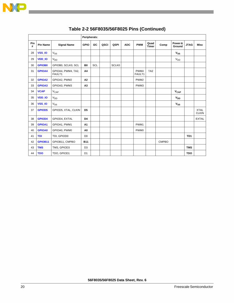
In Table 2-2, peripheral pins in bold identify reset state.
Table 2-2 56F8035/56F8025 PinsPeripherals:
Pin # Pin Name Signal Name GPIO I2C QSCI QSPI ADC PWM Quad
Timer Comp Power & Ground JTAG Misc
1 GPIOB6 GPIOB6, RXD0, SDA, CLKIN
B6 SDA RXD0 CLKIN
2 GPIOB1 GPIOB1, SS0, SDA B1 SDA SS0
3 GPIOB7 GPIOB7, TXD0, SCL B7 SCL TXD0
4 GPIOB5 GPIOB5, TA1, FAULT3, CLKIN
B5 FAULT3 TA1 CLKIN
5 GPIOA9 GPIOA9, FAULT2, TA3, CMPBI1
A9 FAULT2 TA3 CMPBI1
6 GPIOA11 GPIOA11, CMPBI2 A11 CMPBI2
7 GPIOC4 GPIOC4, ANB0, CMPBI3
C4 ANB0 CMPBI3
8 GPIOC5 GPIOC5, ANB1 C5 ANB1
9 GPIOC6 GPIOC6, ANB2, VREFHB
C6 ANB2 VREFHB
10 GPIOC7 GPIOC7, ANB3, VREFLB
C7 ANB3VREFLB
11 VDDA VDDA VDDA
12 VSSA VSSA VSSA
13 GPIOC3 GPIOC3, ANA3, VREFLA
C3 ANA3VREFLA
14 GPIOC2 GPIOC2, ANA2, VREFHA
C2 ANA2VREFHA
15 GPIOC1 GPIOC1, ANA1 C1 ANA1
16 GPIOC0 GPIOC0, ANA0, CMPAI3
C0 ANA0 CMPAI3
17 VSS_IO VSS VSS
18 VCAP VCAP VCAP
19 TCK TCK, GPIOD2 D2 TCK
20 GPIOB10 GPIOB10, CMPAO B10 CMPAO
21 RESET RESET, GPIOA7 A7 RESET
22 GPIOB3 GPIOB3, MOSI0, TA3, PSRC1
B3 MOSI0 PSRC1 TA3
23 GPIOB2 GPIOB2, MISO0, TA2, PSRC0
B2 MISO0 PSRC0 TA2
24 GPIOA6 GPIOA6, FAULT0, TA0
A6 FAULT0 TA0
25 GPIOA10 GPIOA10, CMPAI2 A10 CMPAI2
26 GPIOA8 GPIOA8, FAULT1, TA2, CMPAI1
A8 FAULT1 TA2 CMPAI1
27 GPIOA5 GPIOA5, PWM5, TA3, FAULT2
A5 PWM5FAULT2
TA3
56F8035/56F8025 Data Sheet, Rev. 6
20 Freescale Semiconductor
28 VSS_IO VSS VSS
29 VDD_IO VDD VDD
30 GPIOB0 GPIOB0, SCLK0, SCL B0 SCL SCLK0
31 GPIOA4 GPIOA4, PWM4, TA2, FAULT1
A4 PWM4FAULT1
TA2
32 GPIOA2 GPIOA2, PWM2 A2 PWM2
33 GPIOA3 GPIOA3, PWM3 A3 PWM3
34 VCAP VCAP VCAP
35 VDD_IO VDD VDD
36 VSS_IO VSS VSS
37 GPIOD5 GPIOD5, XTAL, CLKIN D5 XTALCLKIN
38 GPIOD4 GPIOD4, EXTAL D4 EXTAL
39 GPIOA1 GPIOA1, PWM1 A1 PWM1
40 GPIOA0 GPIOA0, PWM0 A0 PWM0
41 TDI TDI, GPIOD0 D0 TD1
42 GPIOB11 GPIOB11, CMPBO B11 CMPBO
43 TMS TMS, GPIOD3 D3 TMS
44 TDO TDO, GPIOD1 D1 TDO
Table 2-2 56F8035/56F8025 Pins (Continued)Peripherals:
Pin # Pin Name Signal Name GPIO I2C QSCI QSPI ADC PWM Quad
Timer Comp Power & Ground JTAG Misc
Introduction
56F8035/56F8025 Data Sheet, Rev. 6
Freescale Semiconductor 21
Figure 2-1 56F8035/56F8025 Signals Identified by Functional Group
VDD
VDDA
VSSA
GPIOD5 (XTAL, CLKIN)
GPIOD4 (EXTAL)
OtherSupply
Ports
OSC Portor GPIO
JTAG/ EOnCEor GPIOD
2
1
3
VCAP2
1
1
TCK (GPIOD2)
TMS (GPIOD3)
GPIOC2 (ANA2, VREFHA)
1
1
1
56F8035/56F802
1
TDI (GPIOD0)
TDO (GPIOD1)
GPIOB5 (TA1, FAULT3, CLKIN)
GPIOB6 (RXD0, SDA, CLKIN)
GPIOB7 (TXD0, SCL)
1
1
1
VSS
Power
Ground
Power
Ground
GPIOC1 (ANA1)1
GPIOC0 (ANA0 & CMPAI3)1
GPIOC3 (ANA3, VREFLA)1
RESETor GPIOA
RESET (GPIOA7)1
GPIOB0 (SCLK0, SCL)
GPIOB1 (SS0, SDA)QSPIor I2C
or PWMor TMRA
or GPIOB
1
1
QSCIor PWM
or I2Cor TMRAor QSPI
or GPIOB
ADCor CMPor GPIOC
GPIOB2 (MISO0, TA2, PSRC0)
GPIOB3 (MOSI0, TA3, PSRC1)1
1
GPIOA9 (FAULT2, TA3, CMPBI1)1
GPIOA0-3 (PWM0-3)
GPIOA4 (PWM4, TA2, FAULT1)
GPIOA5 (PWM5, TA3, FAULT2)
4
1
1
GPIOA8 (FAULT1, TA2, CMPAI1)1
GPIOA6 (FAULT0, TA0)1
GPIOA10 (CMPAI2)1
GPIOA11 (CMPBI2)1
PWMor TMRAor CMPor GPIOA
1
1
1
GPIOB10 (CMPAO)1
GPIOB11 (CMPBO)1
CMPor GPIOB
GPIOC6 (ANB2, VREFHA)1
GPIOC5 (ANB1)1
GPIOC4 (ANB0 & CMPBI3)1
GPIOC7 (ANB3, VREFLB)1

56F8035/56F8025 Data Sheet, Rev. 6
22 Freescale Semiconductor
2.2 56F8035/56F8025 Signal PinsAfter reset, each pin is configured for its primary function (listed first). Any alternate functionality mustbe programmed.
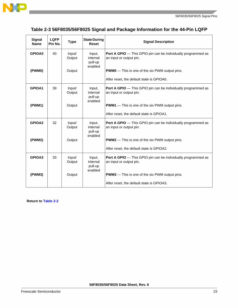
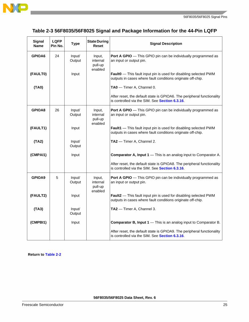
Table 2-3 56F8035/56F8025 Signal and Package Information for the 44-Pin LQFP
Signal Name
LQFP Pin No. Type State During
Reset Signal Description
VDD 29 Supply Supply I/O Power — This pin supplies 3.3V power to the chip I/O interface.
VDD 35
VSS 17 Supply Supply VSS — These pins provide ground for chip logic and I/O drivers.
VSS 28
VSS 36
VDDA 11 Supply Supply ADC Power — This pin supplies 3.3V power to the ADC modules. It must be connected to a clean analog power supply.
VSSA 12 Supply Supply ADC Analog Ground — This pin supplies an analog ground to the ADC modules.
VCAP 18 Supply Supply VCAP — Connect this pin to a 2.2μF or greater bypass capacitor in order to bypass the core voltage regulator, required for proper chip operation. See Section 10.2.1.VCAP 34
RESET
(GPIOA7)
21 Input
Input/Open Drain
Output
Input, internal pull-up
enabled
Reset — This input is a direct hardware reset on the processor. When RESET is asserted low, the chip is initialized and placed in the reset state. A Schmitt trigger input is used for noise immunity. The internal reset signal will be deasserted synchronous with the internal clocks after a fixed number of internal clocks.
Port A GPIO — This GPIO pin can be individually programmed as an input or open drain output pin. Note that RESET functionality is disabled in this mode and the chip can only be reset via POR, COP reset, or software reset.
After reset, the default state is RESET.
Return to Table 2-2
56F8035/56F8025 Signal Pins
56F8035/56F8025 Data Sheet, Rev. 6
Freescale Semiconductor 23
GPIOA0
(PWM0)
40 Input/Output
Output
Input, internal pull-up
enabled
Port A GPIO — This GPIO pin can be individually programmed as an input or output pin.
PWM0 — This is one of the six PWM output pins.
After reset, the default state is GPIOA0.
GPIOA1
(PWM1)
39 Input/Output
Output
Input, internal pull-up
enabled
Port A GPIO — This GPIO pin can be individually programmed as an input or output pin.
PWM1 — This is one of the six PWM output pins.
After reset, the default state is GPIOA1.
GPIOA2
(PWM2)
32 Input/Output
Output
Input, internal pull-up
enabled
Port A GPIO — This GPIO pin can be individually programmed as an input or output pin.
PWM2 — This is one of the six PWM output pins.
After reset, the default state is GPIOA2.
GPIOA3
(PWM3)
33 Input/Output
Output
Input, internal pull-up
enabled
Port A GPIO — This GPIO pin can be individually programmed as an input or output pin.
PWM3 — This is one of the six PWM output pins.
After reset, the default state is GPIOA3.
Return to Table 2-2
Table 2-3 56F8035/56F8025 Signal and Package Information for the 44-Pin LQFP
Signal Name
LQFP Pin No. Type State During
Reset Signal Description

56F8035/56F8025 Data Sheet, Rev. 6
24 Freescale Semiconductor
GPIOA4
(PWM4)
(TA21)
(FAULT12)
31 Input/Output
Output
Input/Output
Input
Input, internal pull-up
enabled
Port A GPIO — This GPIO pin can be individually programmed as an input or output pin.
PWM4 — This is one of the six PWM output pins.
TA2 — Timer A, Channel 2
Fault1 — This fault input pin is used for disabling selected PWM outputs in cases where fault conditions originate off-chip.
After reset, the default state is GPIOA4. The peripheral functionality is controlled via the SIM. See Section 6.3.16.
1The TA2 signal is also brought out on the GPIOA8-9 and GPIOB2-3 pins.2The Fault1 signal is also brought out on the GPIOA8-9 and GPIOB10 pins.
GPIOA5
(PWM5)
(TA33)
(FAULT24)
27 Input/Output
Output
Input/ Output
Input
Input, internal pull-up
enabled
Port A GPIO — This GPIO pin can be individually programmed as an input or output pin.
PWM5 — This is one of the six PWM output pins.
TA3 — Timer A, Channel 3
Fault2 — This fault input pin is used for disabling selected PWM outputs in cases where fault conditions originate off-chip.
After reset, the default state is GPIOA5. The peripheral functionality is controlled via the SIM. See Section 6.3.16.
3The TA3 signal is also brought out on the GPIOA8-9 and GPIOB2-3 pins.4The Fault2 signal is also brought out on the GPIOA8-9 and GPIOB10 pins.
Return to Table 2-2
Table 2-3 56F8035/56F8025 Signal and Package Information for the 44-Pin LQFP
Signal Name
LQFP Pin No. Type State During
Reset Signal Description
56F8035/56F8025 Signal Pins
56F8035/56F8025 Data Sheet, Rev. 6
Freescale Semiconductor 25
GPIOA6
(FAULT0)
(TA0)
24 Input/Output
Input
Input, internal pull-up
enabled
Port A GPIO — This GPIO pin can be individually programmed as an input or output pin.
Fault0 — This fault input pin is used for disabling selected PWM outputs in cases where fault conditions originate off-chip.
TA0 — Timer A, Channel 0.
After reset, the default state is GPIOA6. The peripheral functionality is controlled via the SIM. See Section 6.3.16.
GPIOA8
(FAULT1)
(TA2)
(CMPAI1)
26 Input/Output
Input
Input/Output
Input
Input, internal pull-up
enabled
Port A GPIO — This GPIO pin can be individually programmed as an input or output pin.
Fault1 — This fault input pin is used for disabling selected PWM outputs in cases where fault conditions originate off-chip.
TA2 — Timer A, Channel 2.
Comparator A, Input 1 — This is an analog input to Comparator A.
After reset, the default state is GPIOA8. The peripheral functionality is controlled via the SIM. See Section 6.3.16.
GPIOA9
(FAULT2)
(TA3)
(CMPBI1)
5 Input/Output
Input
Input/Output
Input
Input, internal pull-up
enabled
Port A GPIO — This GPIO pin can be individually programmed as an input or output pin.
Fault2 — This fault input pin is used for disabling selected PWM outputs in cases where fault conditions originate off-chip.
TA2 — Timer A, Channel 3.
Comparator B, Input 1 — This is an analog input to Comparator B.
After reset, the default state is GPIOA9. The peripheral functionality is controlled via the SIM. See Section 6.3.16.
Return to Table 2-2
Table 2-3 56F8035/56F8025 Signal and Package Information for the 44-Pin LQFP
Signal Name
LQFP Pin No. Type State During
Reset Signal Description

56F8035/56F8025 Data Sheet, Rev. 6
26 Freescale Semiconductor
GPIOA10
(CMPAI2)
25 Input/Output
Input
Input, internal pull-up
enabled
Port A GPIO — This GPIO pin can be individually programmed as an input or output pin.
Comparator A, Input 2 — This is an analog input to Comparator A.
After reset, the default state is GPIOA10. The peripheral functionality is controlled via the SIM. See Section 6.3.16.
GPIOA11
(CMPBI2)
6 Input/Output
Input
Input, internal pull-up
enabled
Port A GPIO — This GPIO pin can be individually programmed as an input or output pin.
Comparator B, Input 2 — This is an analog input to Comparator B.
After reset, the default state is GPIOA11. The peripheral functionality is controlled via the SIM. See Section 6.3.16.
GPIOB0
(SCLK0)
(SCL5)
30 Input/Output
Input/Output
Input/Output
Input, internal pull-up
enabled
Port B GPIO — This GPIO pin can be individually programmed as an input or output pin.
QSPI0 Serial Clock — In the master mode, this pin serves as an output, clocking slaved listeners. In slave mode, this pin serves as the data clock input. A Schmitt trigger input is used for noise immunity.
Serial Clock — This pin serves as the I2C serial clock.
After reset, the default state is GPIOB0. The peripheral functionality is controlled via the SIM. See Section 6.3.16.
5The SCL signal is also brought out on the GPIOB7 pin.
GPIOB1
(SS0)
(SDA6)
2 Input/Output
Input/Output
Input
Input, internal pull-up
enabled
Port B GPIO — This GPIO pin can be individually programmed as an input or output pin.
QSPI0 Slave Select — SS is used in slave mode to indicate to the QSPI0 module that the current transfer is to be received.
Serial Data — This pin serves as the I2C serial data line.
After reset, the default state is GPIOB1. The peripheral functionality is controlled via the SIM. See Section 6.3.16.
6The SDA signal is also brought out on the GPIOB6 pin.
Return to Table 2-2
Table 2-3 56F8035/56F8025 Signal and Package Information for the 44-Pin LQFP
Signal Name
LQFP Pin No. Type State During
Reset Signal Description

56F8035/56F8025 Signal Pins
56F8035/56F8025 Data Sheet, Rev. 6
Freescale Semiconductor 27
GPIOB2
(MISO0)
(TA27)
(PSRC0)
23 Input/Output
Input/Output
Input/Output
Input
Input, internal pull-up
enabled
Port B GPIO — This GPIO pin can be individually programmed as an input or output pin.
QSPI0 Master In/Slave Out — This serial data pin is an input to a master device and an output from a slave device. The MISO line of a slave device is placed in the high-impedance state if the slave device is not selected. The slave device places data on the MISO line a half-cycle before the clock edge the master device uses to latch the data.
TA2 — Timer A, Channel 2
PSRC0 — External PWM signal source input for the complementary PWM4/PWM5 pair.
After reset, the default state is GPIOB2. The peripheral functionality is controlled via the SIM. See Section 6.3.16.
7The TA2 signal is also brought out on the GPIOA4 and GPIOA8 pins.
GPIOB3
(MOSI0)
(TA38)
(PSRC1)
22 Input/Output
Input/Output
Input/Output
Input
Input, internal pull-up
enabled
Port B GPIO — This GPIO pin can be individually programmed as an input or output pin.
QSPI0 Master Out/Slave In— This serial data pin is an output from a master device and an input to a slave device. The master device places data on the MOSI line a half-cycle before the clock edge the slave device uses to latch the data.
TA3 — Timer A, Channel 3
PSRC1 — External PWM signal source input for the complementary PWM2/PWM3 pair.
After reset, the default state is GPIOB3. The peripheral functionality is controlled via the SIM. See Section 6.3.16.
8The TA3 signal is also brought out on the GPIOA5 and GPIOA9 pins.
Return to Table 2-2
Table 2-3 56F8035/56F8025 Signal and Package Information for the 44-Pin LQFP
Signal Name
LQFP Pin No. Type State During
Reset Signal Description
56F8035/56F8025 Data Sheet, Rev. 6
28 Freescale Semiconductor
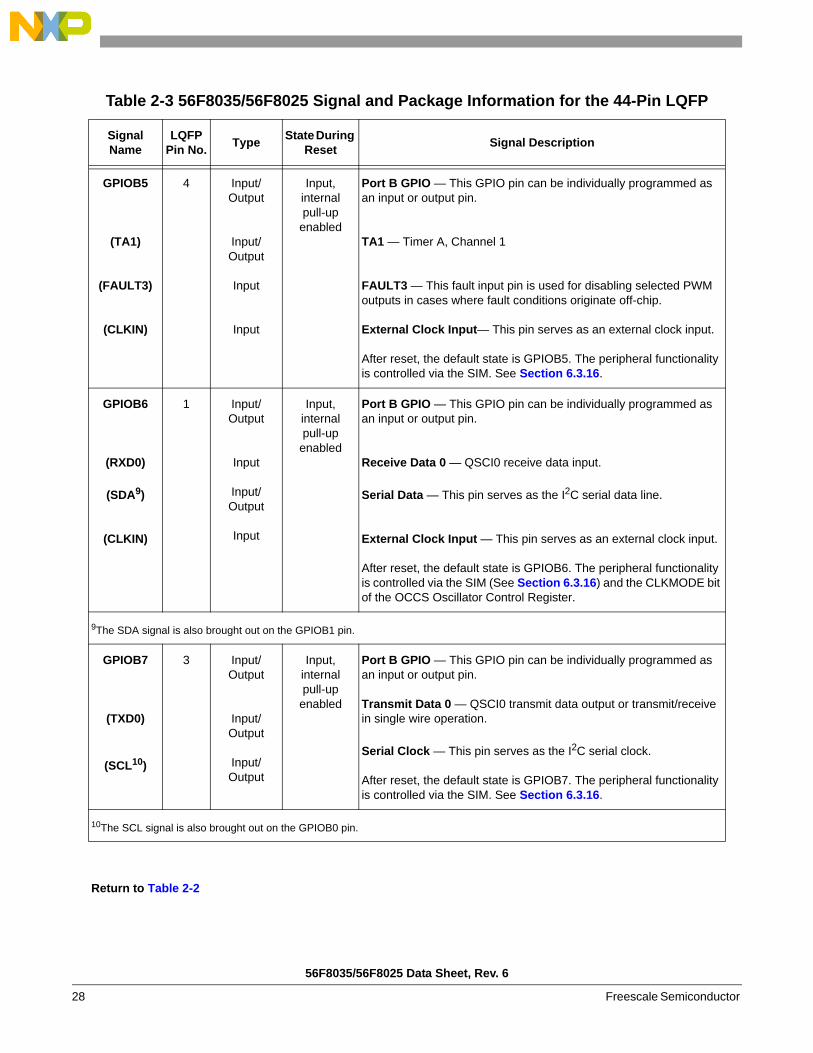
GPIOB5
(TA1)
(FAULT3)
(CLKIN)
4 Input/Output
Input/Output
Input
Input
Input, internal pull-up
enabled
Port B GPIO — This GPIO pin can be individually programmed as an input or output pin.
TA1 — Timer A, Channel 1
FAULT3 — This fault input pin is used for disabling selected PWM outputs in cases where fault conditions originate off-chip.
External Clock Input— This pin serves as an external clock input.
After reset, the default state is GPIOB5. The peripheral functionality is controlled via the SIM. See Section 6.3.16.
GPIOB6
(RXD0)
(SDA9)
(CLKIN)
1 Input/Output
Input
Input/Output
Input
Input, internal pull-up
enabled
Port B GPIO — This GPIO pin can be individually programmed as an input or output pin.
Receive Data 0 — QSCI0 receive data input.
Serial Data — This pin serves as the I2C serial data line.
External Clock Input — This pin serves as an external clock input.
After reset, the default state is GPIOB6. The peripheral functionality is controlled via the SIM (See Section 6.3.16) and the CLKMODE bit of the OCCS Oscillator Control Register.
9The SDA signal is also brought out on the GPIOB1 pin.
GPIOB7
(TXD0)
(SCL10)
3 Input/Output
Input/Output
Input/Output
Input, internal pull-up
enabled
Port B GPIO — This GPIO pin can be individually programmed as an input or output pin.
Transmit Data 0 — QSCI0 transmit data output or transmit/receive in single wire operation.
Serial Clock — This pin serves as the I2C serial clock.
After reset, the default state is GPIOB7. The peripheral functionality is controlled via the SIM. See Section 6.3.16.
10The SCL signal is also brought out on the GPIOB0 pin.
Return to Table 2-2
Table 2-3 56F8035/56F8025 Signal and Package Information for the 44-Pin LQFP
Signal Name
LQFP Pin No. Type State During
Reset Signal Description

56F8035/56F8025 Signal Pins
56F8035/56F8025 Data Sheet, Rev. 6
Freescale Semiconductor 29
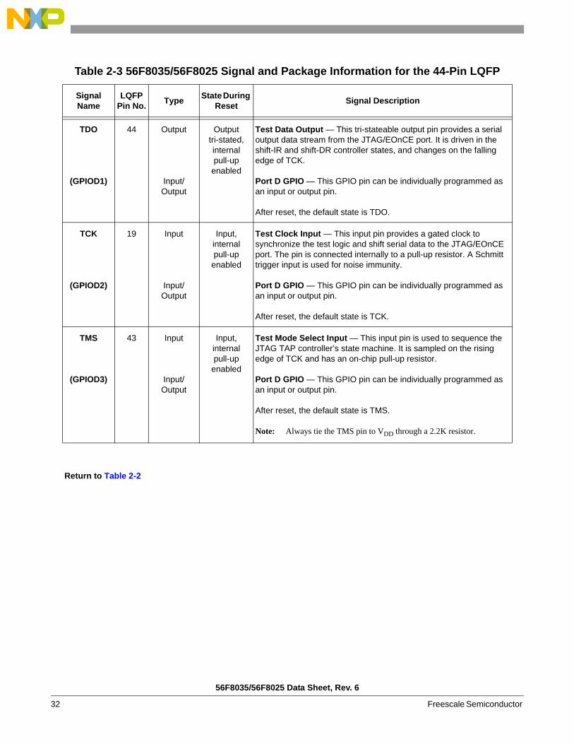
GPIOB10
(CMPAO)
20 Input/Output
Output
Input, internal pull-up
enabled
Port B GPIO — This GPIO pin can be individually programmed as an input or output pin.
Comparator A Output— This is the output of comparator A.
After reset, the default state is GPIOB10. The peripheral functionality is controlled via the SIM. See Section 6.3.16.
GPIOB11
(CMPBO)
42 Input/Output
Output
Input, internal pull-up
enabled
Port B GPIO — This GPIO pin can be individually programmed as an input or output pin.
Comparator B Output— This is the output of comparator B.
After reset, the default state is GPIOB11. The peripheral functionality is controlled via the SIM. See Section 6.3.16.
GPIOC0
(ANA0 & CMPAI3)
16 Input/Output
Analog Input
Input Port C GPIO — This GPIO pin can be individually programmed as an input or output pin.
ANA0 — Analog input to ADC A, Channel 0.
Comparator A, Input 3 — This is an analog input to Comparator A.
When used as an analog input, the signal goes to both the ANA0 and CMPAI3.
After reset, the default state is GPIOC0.
GPIOC1
(ANA1)
15 Input/Output
Analog Input
Input Port C GPIO — This GPIO pin can be individually programmed as an input or output pin.
ANA1 — Analog input to ADC A, Channel 1.
After reset, the default state is GPIOC1.
GPIOC2
(ANA2)
(VREFHA)
14 Input/Output
Analog Input
Analog Input
Input Port C GPIO — This GPIO pin can be individually programmed as an input or output pin.
ANA2 — Analog input to ADC A, Channel 2.
VREFHA — Analog reference voltage high (ADC A).
After reset, the default state is GPIOC2.
Return to Table 2-2
Table 2-3 56F8035/56F8025 Signal and Package Information for the 44-Pin LQFP
Signal Name
LQFP Pin No. Type State During
Reset Signal Description

56F8035/56F8025 Data Sheet, Rev. 6
30 Freescale Semiconductor
GPIOC3
(ANA3)
(VREFLA)
13 Input/Output
Analog Input
Analog Input
Input Port C GPIO — This GPIO pin can be individually programmed as an input or output pin.
ANA3 — Analog input to ADC A, Channel 3.
VREFLA — Analog reference voltage low (ADC A).
After reset, the default state is GPIOC3.
GPIOC4
(ANB0 & CMPBI3)
7 Input/Output
Analog Input
Input Port C GPIO — This GPIO pin can be individually programmed as an input or output pin.
ANB0 — Analog input to ADC B, Channel 0.
Comparator B, Input 3 — This is an analog input to Comparator B.
When used as an analog input, the signal goes to both the ANB0 and CMPBI3.
After reset, the default state is GPIOC4.
GPIOC5
(ANB1)
8 Input/Output
Analog Input
Input Port C GPIO — This GPIO pin can be individually programmed as an input or output pin.
ANB1 — Analog input to ADC B, Channel 1.
After reset, the default state is GPIOC5.
GPIOC6
(ANB2)
(VREFHB)
9 Input/Output
Analog Input
Input
Input Port C GPIO — This GPIO pin can be individually programmed as an input or output pin.
ANB2 — Analog input to ADC B, Channel 2.
VREFHB — Analog reference voltage high (ADC B).
After reset, the default state is GPIOC6.
Return to Table 2-2
Table 2-3 56F8035/56F8025 Signal and Package Information for the 44-Pin LQFP
Signal Name
LQFP Pin No. Type State During
Reset Signal Description

56F8035/56F8025 Signal Pins
56F8035/56F8025 Data Sheet, Rev. 6
Freescale Semiconductor 31
GPIOC7
(ANB3)
(VREFLB)
10 Input/Output
Analog Input
Input
Input Port C GPIO — This GPIO pin can be individually programmed as an input or output pin.
ANB3 — Analog input to ADC B, Channel 3.
VREFLB — Analog reference voltage low (ADC B).
After reset, the default state is GPIOC7.
GPIOD4
(EXTAL)
38 Input/Output
Analog Input
Input Port D GPIO — This GPIO pin can be individually programmed as an input or output pin.
External Crystal Oscillator Input — This input can be connected to an 8MHz external crystal. Tie this pin low if XTAL is being driven by an external clock source.
After reset, the default state is GPIOD4.
GPIOD5
(XTAL)
(CLKIN)
37 Input/Output
Analog Input/Output
Input
Input Port D GPIO — This GPIO pin can be individually programmed as an input or output pin.
External Crystal Oscillator Output — This output connects the internal crystal oscillator output to an external crystal.
External Clock Input — This pin serves as an external clock input.
After reset, the default state is GPIOD5.
TDI
(GPIOD0)
41 Input
Input/Output
Input, internal pull-up
enabled
Test Data Input — This input pin provides a serial input data stream to the JTAG/EOnCE port. It is sampled on the rising edge of TCK and has an on-chip pull-up resistor.
Port D GPIO — This GPIO pin can be individually programmed as an input or output pin.
After reset, the default state is TDI.
Return to Table 2-2
Table 2-3 56F8035/56F8025 Signal and Package Information for the 44-Pin LQFP
Signal Name
LQFP Pin No. Type State During
Reset Signal Description
56F8035/56F8025 Data Sheet, Rev. 6
32 Freescale Semiconductor
TDO
(GPIOD1)
44 Output
Input/Output
Output tri-stated, internal pull-up
enabled
Test Data Output — This tri-stateable output pin provides a serial output data stream from the JTAG/EOnCE port. It is driven in the shift-IR and shift-DR controller states, and changes on the falling edge of TCK.
Port D GPIO — This GPIO pin can be individually programmed as an input or output pin.
After reset, the default state is TDO.
TCK
(GPIOD2)
19 Input
Input/Output
Input, internal pull-up
enabled
Test Clock Input — This input pin provides a gated clock to synchronize the test logic and shift serial data to the JTAG/EOnCE port. The pin is connected internally to a pull-up resistor. A Schmitt trigger input is used for noise immunity.
Port D GPIO — This GPIO pin can be individually programmed as an input or output pin.
After reset, the default state is TCK.
TMS
(GPIOD3)
43 Input
Input/Output
Input, internal pull-up
enabled
Test Mode Select Input — This input pin is used to sequence the JTAG TAP controller’s state machine. It is sampled on the rising edge of TCK and has an on-chip pull-up resistor.
Port D GPIO — This GPIO pin can be individually programmed as an input or output pin.
After reset, the default state is TMS.
Note: Always tie the TMS pin to VDD through a 2.2K resistor.
Return to Table 2-2
Table 2-3 56F8035/56F8025 Signal and Package Information for the 44-Pin LQFP
Signal Name
LQFP Pin No. Type State During
Reset Signal Description

Overview
56F8035/56F8025 Data Sheet, Rev. 6
Freescale Semiconductor 33
Part 3 OCCS
3.1 OverviewThe On-Chip Clock Synthesis (OCCS) module allows designers using an internal relaxation oscillator, anexternal crystal, or an external clock to run 56F8000 family devices at user-selectable frequencies up to32MHz. For details, see the OCCS chapter in the 56F802x and 56F803x Peripheral Reference Manual.
3.2 FeaturesThe OCCS module interfaces to the oscillator and PLL and offers these features:
• Internal relaxation oscillator• Ability to power down the internal relaxation oscillator or crystal oscillator• Ability to put the internal relaxation oscillator into Standby mode• 3-bit postscaler provides control for the PLL output• Ability to power down the PLL• Provides a 2X system clock which operates at twice the system clock to the System Integration Module
(SIM)• Provides a 3X system clock which operates at three times the system clock to PWM and Timer modules• Safety shutdown feature is available if the PLL reference clock is lost• Can be driven from an external clock source
The clock generation module provides the programming interface for the PLL, internal relaxationoscillator, and crystal oscillator.
3.3 Operating ModesIn 56F8000 family devices, an internal oscillator, an external crystal, or an external clock source can beused to provide a reference clock to the SIM.
The 2X system clock source output from the OCCS can be described by one of the following equations:
2X system frequency = oscillator frequency
2X system frequency = (oscillator frequency x 8) / (postscaler)
where:
postscaler = 1, 2, 4, 8, 16, or 32
The SIM is responsible for further dividing these frequencies by two, which will insure a 50% duty cyclein the system clock output.

56F8035/56F8025 Data Sheet, Rev. 6
34 Freescale Semiconductor
The 56F8000 family devices’ on-chip clock synthesis module has the following registers:
• Control Register (OCCS_CTRL)• Divide-by Register (OCCS_DIVBY)• Status Register (OCCS_STAT)• Shutdown Register (OCCS_SHUTDN)• Oscillator Control Register (OCCS_OCTRL)
For more information on these registers, please refer to the 56F802x and 56F803x Peripheral ReferenceManual.
3.4 Internal Clock SourceAn internal relaxation oscillator can supply the reference frequency when an external frequency source orcrystal is not used. It is optimized for accuracy and programmability while providing several power-savingconfigurations which accommodate different operating conditions. The internal relaxation oscillator hasvery little temperature and voltage variability. To optimize power, the architecture supports a standby stateand a power-down state.
During a boot or reset sequence, the relaxation oscillator is enabled by default (the PRECS bit in thePLLCR word is set to 0). Application code can then also switch to the external clock source and powerdown the internal oscillator, if desired. If a changeover between internal and external clock sources isrequired at power-on, the user must ensure that the clock source is not switched until the desired externalclock source is enabled and stable.
To compensate for variances in the device manufacturing process, the accuracy of the relaxation oscillatorcan be incrementally adjusted to within + 0.078% of 8MHz by trimming an internal capacitor. Bits 0-9 ofthe OSCTL (oscillator control) register allow the user to set in an additional offset (trim) to this presetvalue to increase or decrease capacitance. Each unit added or subtracted changes the output frequency byabout 0.078% of 8MHz, allowing incremental adjustment until the desired frequency accuracy is achieved.
The center frequency of the internal oscillator is calibrated at the factory to 8MHz and the TRIM value isstored in the Flash information block and loaded to the FMOPT1 register at reset. When using therelaxation oscillator, the boot code should read the FMOPT1 register and set this value as OSCTL TRIM.For further information, see the 56F802x and 56F803x Peripheral Reference Manual.
3.5 Crystal OscillatorThe internal crystal oscillator circuit is designed to interface with a parallel-resonant crystal resonator in afrequency range of 4-8MHz, specified for the external crystal. Figure 3-1 shows a typical crystal oscillatorcircuit. Follow the crystal supplier’s recommendations when selecting a crystal, since crystal parametersdetermine the component values required to provide maximum stability and reliable start-up. The loadcapacitance values used in the oscillator circuit design should include all stray layout capacitances. Thecrystal and associated components should be mounted as near as possible to the EXTAL and XTAL pinsto minimize output distortion and start-up stabilization time.

Ceramic Resonator
56F8035/56F8025 Data Sheet, Rev. 6
Freescale Semiconductor 35
Figure 3-1 External Crystal Oscillator Circuit
3.6 Ceramic ResonatorThe internal crystal oscillator circuit is also designed to interface with a ceramic resonator in the frequencyrange of 4-8MHz. Figure 3-2 shows the typical 2- and 3-terminal ceramic resonators and their circuits.Follow the resonator supplier’s recommendations when selecting a resonator, since their parametersdetermine the component values required to provide maximum stability and reliable start up. The loadcapacitance values used in the resonator circuit design should include all stray layout capacitances. Theresonator and associated components should be mounted as near as possible to the EXTAL and XTAL pinsto minimize output distortion and start-up stabilization time.
Figure 3-2 External Ceramic Resonator Circuit
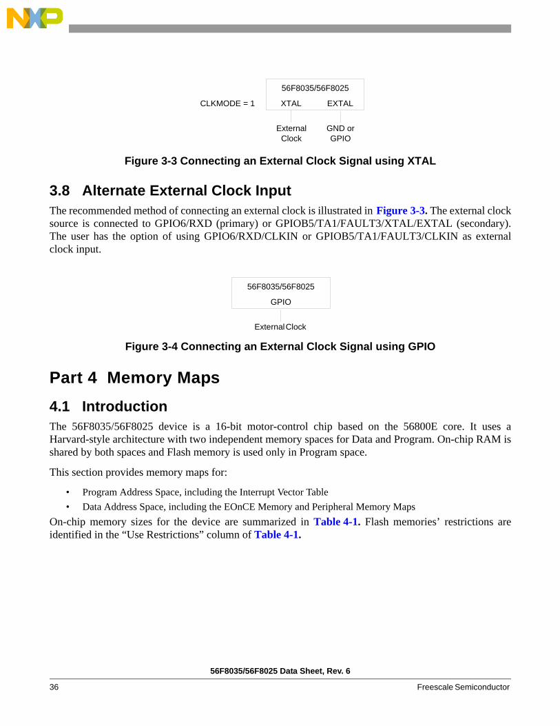
3.7 External Clock Input - Crystal Oscillator OptionThe recommended method of connecting an external clock is illustrated in Figure 3-3. The external clocksource is connected to XTAL and the EXTAL pin is grounded. The external clock input must be generatedusing a relatively low impedance driver.
Sample External Crystal Parameters:Rz = 750 KΩ
Note: If the operating temperature range is limited to below 85oC (105oC junction), then Rz = 10 Meg Ω
EXTAL XTALRz
CL1 CL2
Crystal Frequency = 4 - 8MHz (optimized for 8MHz)
EXTAL XTALRz
EXTAL XTALRz
Sample External Ceramic Resonator Parameters:Rz = 750 KΩ
EXTAL XTALRz
C1CL1 CL2
C2
Resonator Frequency = 4 - 8MHz (optimized for 8MHz)
3 Terminal2 Terminal
56F8035/56F8025 Data Sheet, Rev. 6
36 Freescale Semiconductor
Figure 3-3 Connecting an External Clock Signal using XTAL
3.8 Alternate External Clock InputThe recommended method of connecting an external clock is illustrated in Figure 3-3. The external clocksource is connected to GPIO6/RXD (primary) or GPIOB5/TA1/FAULT3/XTAL/EXTAL (secondary).The user has the option of using GPIO6/RXD/CLKIN or GPIOB5/TA1/FAULT3/CLKIN as externalclock input.
Figure 3-4 Connecting an External Clock Signal using GPIO
Part 4 Memory Maps4.1 IntroductionThe 56F8035/56F8025 device is a 16-bit motor-control chip based on the 56800E core. It uses aHarvard-style architecture with two independent memory spaces for Data and Program. On-chip RAM isshared by both spaces and Flash memory is used only in Program space.
This section provides memory maps for:
• Program Address Space, including the Interrupt Vector Table• Data Address Space, including the EOnCE Memory and Peripheral Memory Maps
On-chip memory sizes for the device are summarized in Table 4-1. Flash memories’ restrictions areidentified in the “Use Restrictions” column of Table 4-1.
56F8035/56F8025
External Clock
XTAL EXTAL
GND or GPIO
CLKMODE = 1
56F8035/56F8025
GPIO
External Clock

Interrupt Vector Table
56F8035/56F8025 Data Sheet, Rev. 6
Freescale Semiconductor 37
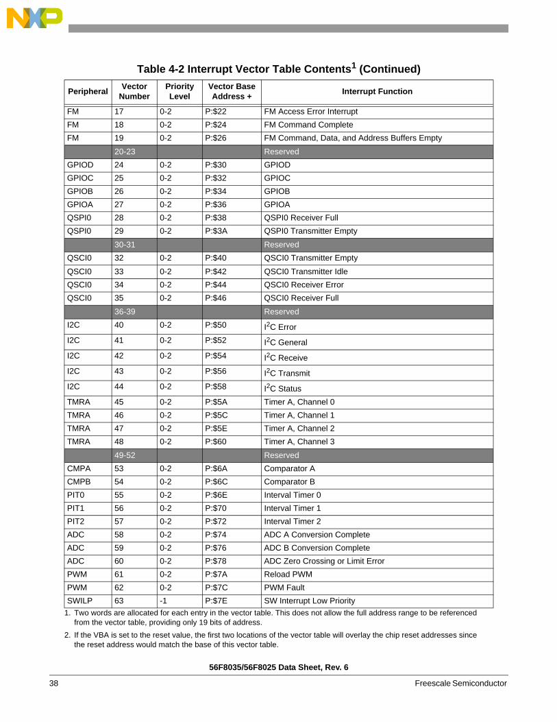
4.2 Interrupt Vector TableTable 4-2 provides the 56F8035/56F8025’s reset and interrupt priority structure, including on-chipperipherals. The table is organized with higher-priority vectors at the top and lower-priority interruptslower in the table. As indicated, the priority of an interrupt can be assigned to different levels, allowingsome control over interrupt priorities. All level 3 interrupts will be serviced before level 2, and so on. Fora selected priority level, the lowest vector number has the highest priority.
The location of the vector table is determined by the Vector Base Address (VBA). Please see Section 5.6.8for the reset value of the VBA.
By default, the chip reset address and COP reset address will correspond to vector 0 and 1 of the interruptvector table. In these instances, the first two locations in the vector table must contain branch or JMPinstructions. All other entries must contain JSR instructions.
Table 4-1 Chip Memory ConfigurationsOn-Chip Memory 56F8035 56F8025 Use Restrictions
Program Flash (PFLASH)32K x 16 or 64KB
16K x 16 or 32KB
Erase/Program via Flash interface unit and word writes to CDBW
Unified RAM (RAM)4K x 16 or 8KB
2K x 16 or 4KB
Usable by both the Program and Data memory spaces
Table 4-2 Interrupt Vector Table Contents1
Peripheral Vector Number
Priority Level
Vector Base Address + Interrupt Function
core P:$00 Reserved for Reset Overlay2 core P:$02 Reserved for COP Reset Overlaycore 2 3 P:$04 Illegal Instruction core 3 3 P:$06 SW Interrupt 3core 4 3 P:$08 HW Stack Overflowcore 5 3 P:$0A Misaligned Long Word Accesscore 6 1-3 P:$0C EOnCE Step Countercore 7 1-3 P:$0E EOnCE Breakpoint Unitcore 8 1-3 P:$10 EOnCE Trace Buffercore 9 1-3 P:$12 EOnCE Transmit Register Emptycore 10 1-3 P:$14 EOnCE Receive Register Fullcore 11 2 P:$16 SW Interrupt 2core 12 1 P:$18 SW Interrupt 1core 13 0 P:$1A SW Interrupt 0
14 Reserved
LVI 15 1-3 P:$1E Low-Voltage Detector (Power Sense)PLL 16 1-3 P:$20 Phase-Locked Loop
56F8035/56F8025 Data Sheet, Rev. 6
38 Freescale Semiconductor
FM 17 0-2 P:$22 FM Access Error InterruptFM 18 0-2 P:$24 FM Command Complete FM 19 0-2 P:$26 FM Command, Data, and Address Buffers Empty
20-23 ReservedGPIOD 24 0-2 P:$30 GPIODGPIOC 25 0-2 P:$32 GPIOCGPIOB 26 0-2 P:$34 GPIOBGPIOA 27 0-2 P:$36 GPIOAQSPI0 28 0-2 P:$38 QSPI0 Receiver FullQSPI0 29 0-2 P:$3A QSPI0 Transmitter Empty
30-31 ReservedQSCI0 32 0-2 P:$40 QSCI0 Transmitter Empty
QSCI0 33 0-2 P:$42 QSCI0 Transmitter IdleQSCI0 34 0-2 P:$44 QSCI0 Receiver ErrorQSCI0 35 0-2 P:$46 QSCI0 Receiver Full
36-39 ReservedI2C 40 0-2 P:$50 I2C ErrorI2C 41 0-2 P:$52 I2C GeneralI2C 42 0-2 P:$54 I2C ReceiveI2C 43 0-2 P:$56 I2C TransmitI2C 44 0-2 P:$58 I2C StatusTMRA 45 0-2 P:$5A Timer A, Channel 0TMRA 46 0-2 P:$5C Timer A, Channel 1TMRA 47 0-2 P:$5E Timer A, Channel 2TMRA 48 0-2 P:$60 Timer A, Channel 3
49-52 ReservedCMPA 53 0-2 P:$6A Comparator ACMPB 54 0-2 P:$6C Comparator BPIT0 55 0-2 P:$6E Interval Timer 0PIT1 56 0-2 P:$70 Interval Timer 1PIT2 57 0-2 P:$72 Interval Timer 2ADC 58 0-2 P:$74 ADC A Conversion CompleteADC 59 0-2 P:$76 ADC B Conversion CompleteADC 60 0-2 P:$78 ADC Zero Crossing or Limit ErrorPWM 61 0-2 P:$7A Reload PWMPWM 62 0-2 P:$7C PWM FaultSWILP 63 -1 P:$7E SW Interrupt Low Priority
1. Two words are allocated for each entry in the vector table. This does not allow the full address range to be referencedfrom the vector table, providing only 19 bits of address.
2. If the VBA is set to the reset value, the first two locations of the vector table will overlay the chip reset addresses sincethe reset address would match the base of this vector table.
Table 4-2 Interrupt Vector Table Contents1 (Continued)
Peripheral Vector Number
Priority Level
Vector Base Address + Interrupt Function

Program Map
56F8035/56F8025 Data Sheet, Rev. 6
Freescale Semiconductor 39
4.3 Program MapThe Program Memory map is shown in Table 4-3 and Table 4-4.
4.4 Data Map
Table 4-3 Program Memory Map1 at Reset for 56F8035
1. All addresses are 16-bit Word addresses.
Begin/End Address Memory Allocation
P: $1F FFFFP: $00 9000
RESERVED
P: $00 8FFFP: $00 8000
On-Chip RAM2
8KB
2. This RAM is shared with Data space starting at address X: $00 0000; see Figure 4-1.
P: $00 7FFFP: $00 0000
Internal Program Flash 64KBCop Reset Address = $00 0002Boot Location = $00 0000
Table 4-4 Program Memory Map1 at Reset for 56F8025
1. All addresses are 16-bit Word addresses.
Begin/End Address Memory Allocation
P: $1F FFFFP: $00 8800
RESERVED
P: $00 87FFP: $00 8000
On-Chip RAM2
4KB
2. This RAM is shared with Data space starting at address X: $00 0000; see Figure 4-2.
P: $00 7FFFP: $00 4000
Internal Program Flash 32KBCop Reset Address = $00 4002Boot Location = $00 4000
P: $00 3FFFP: $00 0000
RESERVED
Table 4-5 Data Memory Map1 for 56F8035Begin/End Address Memory Allocation
X:$FF FFFFX:$FF FF00
EOnCE256 locations allocated
X:$FF FEFFX:$01 0000 RESERVED

56F8035/56F8025 Data Sheet, Rev. 6
40 Freescale Semiconductor
X:$00 FFFFX:$00 F000
On-Chip Peripherals4096 locations allocated
X:$00 EFFFX:$00 8800
RESERVED
X:$00 87FFX:$00 8000
RESERVED
X:$00 7FFFX:$00 1000
RESERVED
X:$00 0FFFX:$00 0000
On-Chip Data RAM8KB2
1. All addresses are 16-bit Word addresses. 2. This RAM is shared with Program space starting at P: $00 8000; see Figure 4-1.
Table 4-6 Data Memory Map1 for 56F8025
1. All addresses are 16-bit Word addresses.
Begin/End Address Memory Allocation
X:$FF FFFFX:$FF FF00
EOnCE256 locations allocated
X:$FF FEFFX:$01 0000 RESERVED
X:$00 FFFFX:$00 F000
On-Chip Peripherals4096 locations allocated
X:$00 EFFFX:$00 8800
RESERVED
X:$00 87FFX:$00 8000
RESERVED
X:$00 7FFFX:$00 0800
RESERVED
X:$00 07FFX:$00 0000
On-Chip Data RAM2
4KB
2. This RAM is shared with Program space starting at P: $00 8000; see Figure 4-2.
Table 4-5 Data Memory Map1 for 56F8035 (Continued)Begin/End Address Memory Allocation
EOnCE Memory Map
56F8035/56F8025 Data Sheet, Rev. 6
Freescale Semiconductor 41
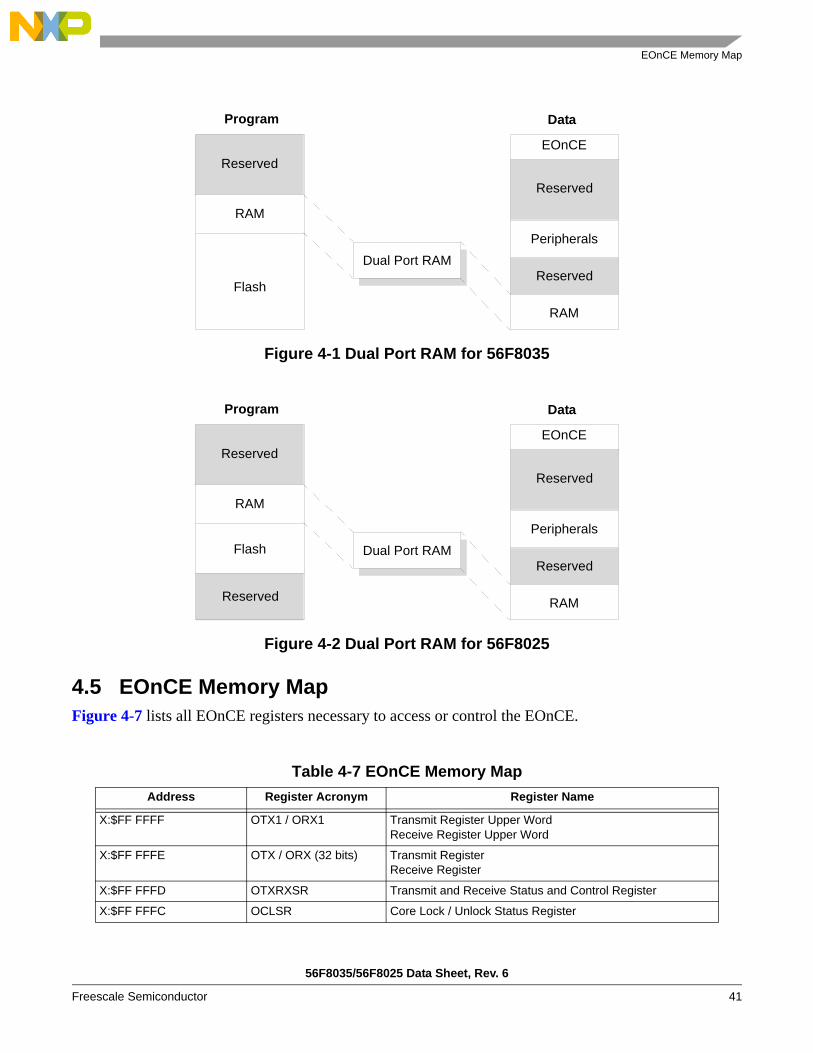
Figure 4-1 Dual Port RAM for 56F8035
Figure 4-2 Dual Port RAM for 56F8025
4.5 EOnCE Memory MapFigure 4-7 lists all EOnCE registers necessary to access or control the EOnCE.
Table 4-7 EOnCE Memory Map Address Register Acronym Register Name
X:$FF FFFF OTX1 / ORX1 Transmit Register Upper WordReceive Register Upper Word
X:$FF FFFE OTX / ORX (32 bits) Transmit RegisterReceive Register
X:$FF FFFD OTXRXSR Transmit and Receive Status and Control Register
X:$FF FFFC OCLSR Core Lock / Unlock Status Register
Reserved
RAM
Flash
Reserved
EOnCE
Peripherals
Reserved
RAM
Dual Port RAM
Program Data
Reserved
RAM
Flash
Reserved
EOnCE
Peripherals
Reserved
RAM
Dual Port RAM
Program Data
Reserved

56F8035/56F8025 Data Sheet, Rev. 6
42 Freescale Semiconductor
4.6 Peripheral Memory-Mapped RegistersOn-chip peripheral registers are part of the data memory map on the 56800E series. These locations maybe accessed with the same addressing modes used for ordinary Data memory, except all peripheralregisters should be read or written using word accesses only.
Table 4-8 summarizes base addresses for the set of peripherals on the 56F8035/56F8025 device.Peripherals are listed in order of the base address.
The following tables list all of the peripheral registers required to control or access the peripherals.
X:$FF FFFB - X:$FF FFA1 Reserved
X:$FF FFA0 OCR Control Register
X:$FF FF9F Instruction Step Counter
X:$FF FF9E OSCNTR (24 bits) Instruction Step Counter
X:$FF FF9D OSR Status Register
X:$FF FF9C OBASE Peripheral Base Address Register
X:$FF FF9B OTBCR Trace Buffer Control Register
X:$FF FF9A OTBPR Trace Buffer Pointer Register
X:$FF FF99 Trace Buffer Register Stages
X:$FF FF98 OTB (21 - 24 bits/stage) Trace Buffer Register Stages
X:$FF FF97 Breakpoint Unit Control Register
X:$FF FF96 OBCR (24 bits) Breakpoint Unit Control Register
X:$FF FF95 Breakpoint Unit Address Register 1
X:$FF FF94 OBAR1 (24 bits) Breakpoint Unit Address Register 1
X:$FF FF93 Breakpoint Unit Address Register 2
X:$FF FF92 OBAR2 (32 bits) Breakpoint Unit Address Register 2
X:$FF FF91 Breakpoint Unit Mask Register 2
X:$FF FF90 OBMSK (32 bits) Breakpoint Unit Mask Register 2
X:$FF FF8F Reserved
X:$FF FF8E OBCNTR EOnCE Breakpoint Unit Counter
X:$FF FF8D Reserved
X:$FF FF8C Reserved
X:$FF FF8B Reserved
X:$FF FF8A OESCR External Signal Control Register
X:$FF FF89 - X:$FF FF00 Reserved
Table 4-8 Data Memory Peripheral Base Address Map SummaryPeripheral Prefix Base Address Table Number
Timer A TMRA X:$00 F000 4-9
Table 4-7 EOnCE Memory Map (Continued)Address Register Acronym Register Name

Peripheral Memory-Mapped Registers
56F8035/56F8025 Data Sheet, Rev. 6
Freescale Semiconductor 43
ADC ADC X:$00 F080 4-10PWM PWM X:$00 F0C0 4-11ITCN ITCN X:$00 F0E0 4-12SIM SIM X:$00 F100 4-13COP COP X:$00 F120 4-14CLK, PLL, OSC OCCS X:$00 F130 4-15Power Supervisor PS X:$00 F140 4-16GPIO Port A GPIOA X:$00 F150 4-17GPIO Port B GPIOB X:$00 F160 4-18GPIO Port C GPIOC X:$00 F170 4-19GPIO Port D GPIOD X:$00 F180 4-20PIT 0 PIT0 X:$00 F190 4-21PIT 1 PIT1 X:$00 F1A0 4-22PIT 2 PIT2 X:$00 F1B0 4-23DAC 0 DAC0 X:$00 F1C0 4-24DAC 1 DAC1 X:$00 F1D0 4-25Comparator A CMPA X:$00 F1E0 4-26Comparator B CMPB X:$00 F1F0 4-27QSCI 0 SCI0 X:$00 F200 4-28QSPI 0 SPI0 X:$00 F220 4-29
I2C I2C X:$00 F280 4-30
FM FM X:$00 F400 4-31
Table 4-9 Quad Timer A Registers Address Map(TMRA_BASE = $00 F000)
Register Acronym Address Offset Register Description
TMRA0_COMP1 $0 Compare Register 1
TMRA0_COMP2 $1 Compare Register 2
TMRA0_CAPT $2 Capture Register
TMRA0_LOAD $3 Load Register
TMRA0_HOLD $4 Hold Register
TMRA0_CNTR $5 Counter Register
TMRA0_CTRL $6 Control Register
TMRA0_SCTRL $7 Status and Control Register
TMRA0_CMPLD1 $8 Comparator Load Register 1
TMRA0_CMPLD2 $9 Comparator Load Register 2
TMRA0_CSCTRL $A Comparator Status and Control Register
TMRA0_FILT $B Input Filter Register
Reserved
Table 4-8 Data Memory Peripheral Base Address Map Summary (Continued)Peripheral Prefix Base Address Table Number

56F8035/56F8025 Data Sheet, Rev. 6
44 Freescale Semiconductor
TMRA0_ENBL $F Timer Channel Enable Register
TMRA1_COMP1 $10 Compare Register 1
TMRA1_COMP2 $11 Compare Register 2
TMRA1_CAPT $12 Capture Register
TMRA1_LOAD $13 Load Register
TMRA1_HOLD $14 Hold Register
TMRA1_CNTR $15 Counter Register
TMRA1_CTRL $16 Control Register
TMRA1_SCTRL $17 Status and Control Register
TMRA1_CMPLD1 $18 Comparator Load Register 1
TMRA1_CMPLD2 $19 Comparator Load Register 2
TMRA1_CSCTRL $1A Comparator Status and Control Register
TMRA1_FILT $1B Input Filter Register
Reserved
TMRA2_COMP1 $20 Compare Register 1
TMRA2_COMP2 $21 Compare Register 2
TMRA2_CAPT $22 Capture Register
TMRA2_LOAD $23 Load Register
TMRA2_HOLD $24 Hold Register
TMRA2_CNTR $25 Counter Register
TMRA2_CTRL $26 Control Register
TMRA2_SCTRL $27 Status and Control Register
TMRA2_CMPLD1 $28 Comparator Load Register 1
TMRA2_CMPLD2 $29 Comparator Load Register 2
TMRA2_CSCTRL $2A Comparator Status and Control Register
TMRA2_FILT $2B Input Filter Register
Reserved
TMRA3_COMP1 $30 Compare Register 1
TMRA3_COMP2 $31 Compare Register 2
TMRA3_CAPT $32 Capture Register
TMRA3_LOAD $33 Load Register
TMRA3_HOLD $34 Hold Register
TMRA3_CNTR $35 Counter Register
TMRA3_CTRL $36 Control Register
TMRA3_SCTRL $37 Status and Control Register
TMRA3_CMPLD1 $38 Comparator Load Register 1
TMRA3_CMPLD2 $39 Comparator Load Register 2
Table 4-9 Quad Timer A Registers Address Map (Continued)(TMRA_BASE = $00 F000)
Register Acronym Address Offset Register Description

Peripheral Memory-Mapped Registers
56F8035/56F8025 Data Sheet, Rev. 6
Freescale Semiconductor 45
TMRA3_CSCTRL $3A Comparator Status and Control Register
TMRA3_FILT $3B Input Filter Register
Reserved
Table 4-10 Analog-to-Digital Converter Registers Address Map(ADC_BASE = $00 F080)
Register Acronym Address Offset Register Description
ADC_CTRL1 $0 Control Register 1
ADC_CTRL2 $1 Control Register 2
ADC_ZXCTRL $2 Zero Crossing Control Register
ADC_CLIST 1 $3 Channel List Register 1
ADC_CLIST 2 $4 Channel List Register 2
ADC_CLIST 3 $5 Channel List Register 3
ADC_CLIST 4 $6 Channel List Register 4
ADC_SDIS $7 Sample Disable Register
ADC_STAT $8 Status Register
ADC_RDY $9 Conversion Ready Register
ADC_LIMSTAT $A Limit Status Register
ADC_ZXSTAT $B Zero Crossing Status Register
ADC_RSLT0 $C Result Register 0
ADC_RSLT1 $D Result Register 1
ADC_RSLT2 $E Result Register 2
ADC_RSLT3 $F Result Register 3
ADC_RSLT4 $10 Result Register 4
ADC_RSLT5 $11 Result Register 5
ADC_RSLT6 $12 Result Register 6
ADC_RSLT7 $13 Result Register 7
ADC_RSLT8 $14 Result Register 8
ADC_RSLT9 $15 Result Register 9
ADC_RSLT10 $16 Result Register 10
ADC_RSLT11 $17 Result Register 11
ADC_RSLT12 $18 Result Register 12
ADC_RSLT13 $19 Result Register 13
ADC_RSLT14 $1A Result Register 14
ADC_RSLT15 $1B Result Register 15
ADC_LOLIM0 $1C Low Limit Register 0
Table 4-9 Quad Timer A Registers Address Map (Continued)(TMRA_BASE = $00 F000)
Register Acronym Address Offset Register Description

56F8035/56F8025 Data Sheet, Rev. 6
46 Freescale Semiconductor
ADC_LOLIM1 $1D Low Limit Register 1
ADC_LOLIM2 $1E Low Limit Register 2
ADC_LOLIM3 $1F Low Limit Register 3
ADC_LOLIM4 $20 Low Limit Register 4
ADC_LOLIM5 $21 Low Limit Register 5
ADC_LOLIM6 $22 Low Limit Register 6
ADC_LOLIM7 $23 Low Limit Register 7
ADC_HILIM0 $24 High Limit Register 0
ADC_HILIM1 $25 High Limit Register 1
ADC_HILIM2 $26 High Limit Register 2
ADC_HILIM3 $27 High Limit Register 3
ADC_HILIM4 $28 High Limit Register 4
ADC_HILIM5 $29 High Limit Register 5
ADC_HILIM6 $2A High Limit Register 6
ADC_HILIM7 $2B High Limit Register 7
ADC_OFFST0 $2C Offset Register 0
ADC_OFFST1 $2D Offset Register 1
ADC_OFFST2 $2E Offset Register 2
ADC_OFFST3 $2F Offset Register 3
ADC_OFFST4 $30 Offset Register 4
ADC_OFFST5 $31 Offset Register 5
ADC_OFFST6 $32 Offset Register 6
ADC_OFFST7 $33 Offset Register 7
ADC_PWR $34 Power Control Register
ADC_CAL $35 Calibration Register
Reserved
Table 4-11 Pulse Width Modulator Registers Address Map(PWM_BASE = $00 F0C0)
Register Acronym Address Offset Register Description
PWM_CTRL $0 Control Register
PWM_FCTRL $1 Fault Control Register
PWM_FLTACK $2 Fault Status Acknowledge Register
PWM_OUT $3 Output Control Register
PWM_CNTR $4 Counter Register
PWM_CMOD $5 Counter Modulo Register
PWM_VAL0 $6 Value Register 0
Table 4-10 Analog-to-Digital Converter Registers Address Map (Continued)(ADC_BASE = $00 F080)
Register Acronym Address Offset Register Description

Peripheral Memory-Mapped Registers
56F8035/56F8025 Data Sheet, Rev. 6
Freescale Semiconductor 47
PWM_VAL1 $7 Value Register 1
PWM_VAL2 $8 Value Register 2
PWM_VAL3 $9 Value Register 3
PWM_VAL4 $A Value Register 4
PWM_VAL5 $B Value Register 5
PWM_DTIM0 $C Dead Time Register 0
PWM_DTIM1 $D Dead Time Register 1
PWM_DMAP1 $E Disable Mapping Register 1
PWM_DMAP2 $F Disable Mapping Register 2
PWM_CNFG $10 Configure Register
PWM_CCTRL $11 Channel Control Register
PWM_PORT $12 Port Register
PWM_ICCTRL $13 Internal Correction Control Register
PWM_SCTRL $14 Source Control Register
PWM_SYNC $15 Synchronization Window Register
PWM_FFILT0 $16 Fault0 Filter Register
PWM_FFILT1 $17 Fault1 Filter Register
PWM_FFILT2 $18 Fault2 Filter Register
PWM_FFILT3 $19 Fault3 Filter Register
Table 4-12 Interrupt Control Registers Address Map(ITCN_BASE = $00 F0E0)
Register Acronym Address Offset Register Description
ITCN_IPR0 $0 Interrupt Priority Register 0
ITCN_IPR1 $1 Interrupt Priority Register 1
ITCN_IPR2 $2 Interrupt Priority Register 2
ITCN_IPR3 $3 Interrupt Priority Register 3
ITCN_IPR4 $4 Interrupt Priority Register 4
ITCN_IPR5 $5 Interrupt Priority Register 5
ITCN_IPR6 $6 Interrupt Priority Register 6
ITCN_VBA $7 Vector Base Address Register
ITCN_FIM0 $8 Fast Interrupt Match 0 Register
ITCN_FIVAL0 $9 Fast Interrupt Vector Address Low 0 Register
ITCN_FIVAH0 $A Fast Interrupt Vector Address High 0 Register
ITCN_FIM1 $B Fast Interrupt Match 1 Register
ITCN_FIVAL1 $C Fast Interrupt Vector Address Low 1 Register
ITCN_FIVAH1 $D Fast Interrupt Vector Address High 1 Register
Table 4-11 Pulse Width Modulator Registers Address Map (Continued)(PWM_BASE = $00 F0C0)
Register Acronym Address Offset Register Description

56F8035/56F8025 Data Sheet, Rev. 6
48 Freescale Semiconductor
ITCN_IRQP0 $E IRQ Pending Register 0
ITCN_IRQP1 $F IRQ Pending Register 1
ITCN_IRQP2 $10 IRQ Pending Register 2
ITCN_IRQP3 $11 IRQ Pending Register 3
Reserved
ITCN_ICTRL $16 Interrupt Control Register
Reserved
Table 4-13 SIM Registers Address Map(SIM_BASE = $00 F100)
Register Acronym Address Offset Register Description
SIM_CTRL $0 Control Register
SIM_RSTAT $1 Reset Status Register
SIM_SWC0 $2 Software Control Register 0
SIM_SWC1 $3 Software Control Register 1
SIM_SWC2 $4 Software Control Register 2
SIM_SWC3 $5 Software Control Register 3
SIM_MSHID $6 Most Significant Half JTAG ID
SIM_LSHID $7 Least Significant Half JTAG ID
SIM_PWR $8 Power Control Register
Reserved
SIM_CLKOUT $A Clock Out Select Register
SIM_PCR $B Peripheral Clock Rate Register
SIM_PCE0 $C Peripheral Clock Enable Register 0
SIM_PCE1 $D Peripheral Clock Enable Register 1
SIM_SD0 $E Peripheral STOP Disable Register 0
SIM_SD1 $F Peripheral STOP Disable Register 1
SIM_IOSAHI $10 I/O Short Address Location High Register
SIM_IOSALO $11 I/O Short Address Location Low Register
SIM_PROT $12 Protection Register
SIM_GPSA0 $13 GPIO Peripheral Select Register 0 for GPIOA
SIM_GPSA1 $14 GPIO Peripheral Select Register 1 for GPIOA
SIM_GPSB0 $15 GPIO Peripheral Select Register 0 for GPIOB
SIM_GPSB1 $16 GPIO Peripheral Select Register 1 for GPIOB
SIM_GPSCD $17 GPIO Peripheral Select Register for GPIOC and GPIOD
SIM_IPS0 $18 Internal Peripheral Source Select Register 0 for PWM
SIM_IPS1 $19 Internal Peripheral Source Select Register 1 for DACs
Table 4-12 Interrupt Control Registers Address Map (Continued)(ITCN_BASE = $00 F0E0)
Register Acronym Address Offset Register Description

Peripheral Memory-Mapped Registers
56F8035/56F8025 Data Sheet, Rev. 6
Freescale Semiconductor 49
SIM_IPS2 $1A Internal Peripheral Source Select Register 2 for TMRA
Reserved
Table 4-14 Computer Operating Properly Registers Address Map(COP_BASE = $00 F120)
Register Acronym Address Offset Register Description
COP_CTRL $0 Control Register
COP_TOUT $1 Time-Out Register
COP_CNTR $2 Counter Register
Table 4-15 Clock Generation Module Registers Address Map(OCCS_BASE = $00 F130)
Register Acronym Address Offset Register Description
OCCS_CTRL $0 Control Register
OCCS_DIVBY $1 Divide-By Register
OCCS_STAT $2 Status Register
Reserved
OCCS_OCTRL $5 Oscillator Control Register
OCCS_CLKCHK $6 Clock Check Register
OCCS_PROT $7 Protection Register
Table 4-16 Power Supervisor Registers Address Map(PS_BASE = $00 F140)
Register Acronym Address Offset Register Description
PS_CTRL $0 Control Register
PS_STAT $1 Status Register
Reserved
Table 4-13 SIM Registers Address Map (Continued)(SIM_BASE = $00 F100)
Register Acronym Address Offset Register Description

56F8035/56F8025 Data Sheet, Rev. 6
50 Freescale Semiconductor
Table 4-17 GPIOA Registers Address Map(GPIOA_BASE = $00 F150)
Register Acronym Address Offset Register Description
GPIOA_PUPEN $0 Pull-up Enable Register
GPIOA_DATA $1 Data Register
GPIOA_DDIR $2 Data Direction Register
GPIOA_PEREN $3 Peripheral Enable Register
GPIOA_IASSRT $4 Interrupt Assert Register
GPIOA_IEN $5 Interrupt Enable Register
GPIOA_IEPOL $6 Interrupt Edge Polarity Register
GPIOA_IPEND $7 Interrupt Pending Register
GPIOA_IEDGE $8 Interrupt Edge-Sensitive Register
GPIOA_PPOUTM $9 Push-Pull Output Mode Control Register
GPIOA_RDATA $A Raw Data Input Register
GPIOA_DRIVE $B Output Drive Strength Control Register
Table 4-18 GPIOB Registers Address Map(GPIOB_BASE = $00 F160)
Register Acronym Address Offset Register Description
GPIOB_PUPEN $0 Pull-up Enable Register
GPIOB_DATA $1 Data Register
GPIOB_DDIR $2 Data Direction Register
GPIOB_PEREN $3 Peripheral Enable Register
GPIOB_IASSRT $4 Interrupt Assert Register
GPIOB_IEN $5 Interrupt Enable Register
GPIOB_IEPOL $6 Interrupt Edge Polarity Register
GPIOB_IPEND $7 Interrupt Pending Register
GPIOB_IEDGE $8 Interrupt Edge-Sensitive Register
GPIOB_PPOUTM $9 Push-Pull Output Mode Control Register
GPIOB_RDATA $A Raw Data Input Register
GPIOB_DRIVE $B Output Drive Strength Control Register
Table 4-19 GPIOC Registers Address Map(GPIOC_BASE = $00 F170)
Register Acronym Address Offset Register Description
GPIOC_PUPEN $0 Pull-up Enable Register

Peripheral Memory-Mapped Registers
56F8035/56F8025 Data Sheet, Rev. 6
Freescale Semiconductor 51
GPIOC_DATA $1 Data Register
GPIOC_DDIR $2 Data Direction Register
GPIOC_PEREN $3 Peripheral Enable Register
GPIOC_IASSRT $4 Interrupt Assert Register
GPIOC_IEN $5 Interrupt Enable Register
GPIOC_IEPOL $6 Interrupt Edge Polarity Register
GPIOC_IPEND $7 Interrupt Pending Register
GPIOC_IEDGE $8 Interrupt Edge-Sensitive Register
GPIOC_PPOUTM $9 Push-Pull Output Mode Control Register
GPIOC_RDATA $A Raw Data Input Register
GPIOC_DRIVE $B Output Drive Strength Control Register
Table 4-19 GPIOC Registers Address Map(GPIOC_BASE = $00 F170)
Register Acronym Address Offset Register Description
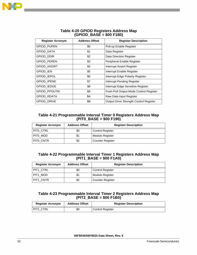
56F8035/56F8025 Data Sheet, Rev. 6
52 Freescale Semiconductor
Table 4-20 GPIOD Registers Address Map(GPIOD_BASE = $00 F180)
Register Acronym Address Offset Register Description
GPIOD_PUPEN $0 Pull-up Enable Register
GPIOD_DATA $1 Data Register
GPIOD_DDIR $2 Data Direction Register
GPIOD_PEREN $3 Peripheral Enable Register
GPIOD_IASSRT $4 Interrupt Assert Register
GPIOD_IEN $5 Interrupt Enable Register
GPIOD_IEPOL $6 Interrupt Edge Polarity Register
GPIOD_IPEND $7 Interrupt Pending Register
GPIOD_IEDGE $8 Interrupt Edge-Sensitive Register
GPIOD_PPOUTM $9 Push-Pull Output Mode Control Register
GPIOD_RDATA $A Raw Data Input Register
GPIOD_DRIVE $B Output Drive Strength Control Register
Table 4-21 Programmable Interval Timer 0 Registers Address Map(PIT0_BASE = $00 F190)
Register Acronym Address Offset Register Description
PIT0_CTRL $0 Control Register
PIT0_MOD $1 Modulo Register
PIT0_CNTR $2 Counter Register
Table 4-22 Programmable Interval Timer 1 Registers Address Map(PIT1_BASE = $00 F1A0)
Register Acronym Address Offset Register Description
PIT1_CTRL $0 Control Register
PIT1_MOD $1 Modulo Register
PIT1_CNTR $2 Counter Register
Table 4-23 Programmable Interval Timer 2 Registers Address Map(PIT2_BASE = $00 F1B0)
Register Acronym Address Offset Register Description
PIT2_CTRL $0 Control Register
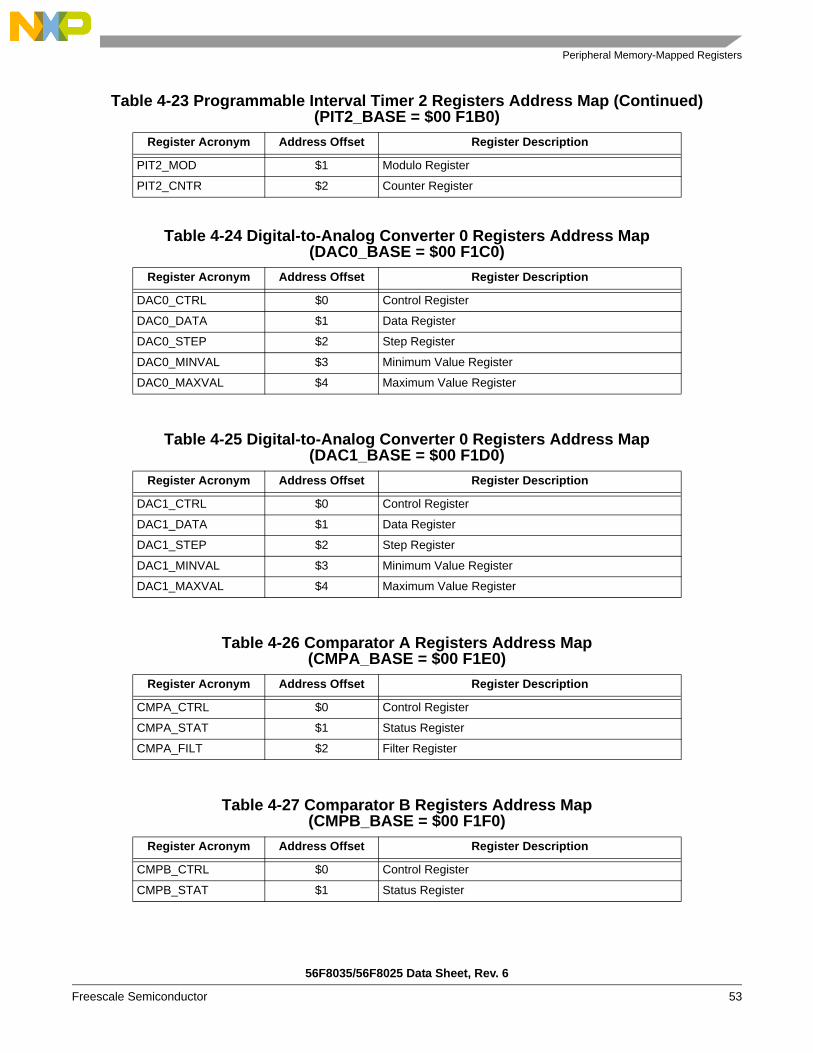
Peripheral Memory-Mapped Registers
56F8035/56F8025 Data Sheet, Rev. 6
Freescale Semiconductor 53
PIT2_MOD $1 Modulo Register
PIT2_CNTR $2 Counter Register
Table 4-24 Digital-to-Analog Converter 0 Registers Address Map(DAC0_BASE = $00 F1C0)
Register Acronym Address Offset Register Description
DAC0_CTRL $0 Control Register
DAC0_DATA $1 Data Register
DAC0_STEP $2 Step Register
DAC0_MINVAL $3 Minimum Value Register
DAC0_MAXVAL $4 Maximum Value Register
Table 4-25 Digital-to-Analog Converter 0 Registers Address Map(DAC1_BASE = $00 F1D0)
Register Acronym Address Offset Register Description
DAC1_CTRL $0 Control Register
DAC1_DATA $1 Data Register
DAC1_STEP $2 Step Register
DAC1_MINVAL $3 Minimum Value Register
DAC1_MAXVAL $4 Maximum Value Register
Table 4-26 Comparator A Registers Address Map(CMPA_BASE = $00 F1E0)
Register Acronym Address Offset Register Description
CMPA_CTRL $0 Control Register
CMPA_STAT $1 Status Register
CMPA_FILT $2 Filter Register
Table 4-27 Comparator B Registers Address Map(CMPB_BASE = $00 F1F0)
Register Acronym Address Offset Register Description
CMPB_CTRL $0 Control Register
CMPB_STAT $1 Status Register
Table 4-23 Programmable Interval Timer 2 Registers Address Map (Continued)(PIT2_BASE = $00 F1B0)
Register Acronym Address Offset Register Description

56F8035/56F8025 Data Sheet, Rev. 6
54 Freescale Semiconductor
CMPB_FILT $2 Filter Register
Table 4-28 Queued Serial Communication Interface 0 Registers Address Map(QSCI0_BASE = $00 F200)
Register Acronym Address Offset Register Description
QSCI0_RATE $0 Baud Rate Register
QSCI0_CTRL1 $1 Control Register 1
QSCI0_CTRL2 $2 Control Register 2
QSCI0_STAT $3 Status Register
QSCI0_DATA $4 Data Register
Table 4-29 Queued Serial Peripheral Interface 0 Registers Address Map(QSPI0_BASE = $00 F220)
Register Acronym Address Offset Register Description
QSPI0_SCTRL $0 Status and Control Register
QSPI0_DSCTRL $1 Data Size and Control Register
QSPI0_DRCV $2 Data Receive Register
QSPI0_DXMIT $3 Data Transmit Register
QSPI0_FIFO $4 FIFO Control Register
QSPI0_DELAY $5 Delay Register
Table 4-30 I2C Registers Address Map(I2C_BASE = $00 F280)
Register Acronym Address Offset Register Description
I2C_CTRL $0 Control Register
I2C_TAR $2 Target Address Register
I2C_SAR $4 Slave Address Register
I2C_DATA $8 RX/TX Data Buffer and Command Register
I2C_SSHCNT $A Standard Speed Clock SCL High Count Register
I2C_SSLCNT $C Standard Speed Clock SCL Low Count Register
I2C_FSHCNT $E Fast Speed Clock SCL High Count Register
I2C_FSLCNT $10 Fast Speed Clock SCL Low Count Register
I2C_ISTAT $16 Interrupt Status Register
I2C_IMASK $18 Interrupt Mask Register
Table 4-27 Comparator B Registers Address Map (Continued)(CMPB_BASE = $00 F1F0)
Register Acronym Address Offset Register Description

Peripheral Memory-Mapped Registers
56F8035/56F8025 Data Sheet, Rev. 6
Freescale Semiconductor 55
I2C_RISTAT $1A Raw Interrupt Status Register
I2C_RXFT $1C Receive FIFO Threshold Register
I2C_TXFT $1E Transmit FIFO Threshold Register
I2C_CLRINT $20 Clear Combined and Individual Interrupts Register
I2C_CLRRXUND $22 Clear RX_UNDER Interrupt Register
I2C_CLRRXOVR $24 Clear RX_OVER Interrupt Register
I2C_CLRTXOVR $26 Clear TX_OVER Interrupt Register
I2C_CLRRDREQ $28 Clear RD_REQ Interrupt Register
I2C_CLRTXABRT $2A Clear TX_ABRT Interrupt Register
I2C_CLRRXDONE $2C Clear RX_DONE Interrupt Register
I2C_CLRACT $2E Clear Activity Interrupt Register
I2C_CLRSTPDET $30 Clear STOP_DET Interrupt Register
I2C_CLRSTDET $32 Clear START_DET Interrupt Register
I2C_CLRGC $34 Clear GEN_CALL Interrupt Register
I2C_ENBL $36 Enable Register
I2C_STAT $38 Status Register
I2C_TXFLR $3A Transmit FIFO Level Register
I2C_RXFLR $3C Receive FIFO Level Register
I2C_TXABRTSRC $40 Transmit Abort Status Register
Table 4-31 Flash Module Registers Address Map(FM_BASE = $00 F400)
Register Acronym Address Offset Register Description
FM_CLKDIV $0 Clock Divider Register
FM_CNFG $1 Configuration Register
$2 Reserved
FM_SECHI $3 Security High Half Register
FM_SECLO $4 Security Low Half Register
$5 - $9 Reserved
FM_PROT $10 Protection Register
$11 - $12 Reserved
FM_USTAT $13 User Status Register
FM_CMD $14 Command Register
$15 - $17 Reserved
FM_DATA $18 Data Buffer Register
$19 - $A Reserved
Table 4-30 I2C Registers Address Map (Continued)(I2C_BASE = $00 F280)
Register Acronym Address Offset Register Description
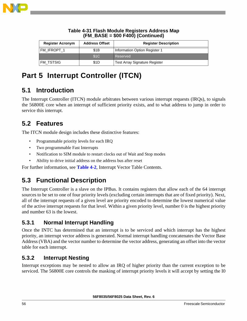
56F8035/56F8025 Data Sheet, Rev. 6
56 Freescale Semiconductor
Part 5 Interrupt Controller (ITCN)
5.1 Introduction The Interrupt Controller (ITCN) module arbitrates between various interrupt requests (IRQs), to signalsthe 56800E core when an interrupt of sufficient priority exists, and to what address to jump in order toservice this interrupt.
5.2 FeaturesThe ITCN module design includes these distinctive features:
• Programmable priority levels for each IRQ• Two programmable Fast Interrupts• Notification to SIM module to restart clocks out of Wait and Stop modes• Ability to drive initial address on the address bus after reset
For further information, see Table 4-2, Interrupt Vector Table Contents.
5.3 Functional DescriptionThe Interrupt Controller is a slave on the IPBus. It contains registers that allow each of the 64 interruptsources to be set to one of four priority levels (excluding certain interrupts that are of fixed priority). Next,all of the interrupt requests of a given level are priority encoded to determine the lowest numerical valueof the active interrupt requests for that level. Within a given priority level, number 0 is the highest priorityand number 63 is the lowest.
5.3.1 Normal Interrupt HandlingOnce the INTC has determined that an interrupt is to be serviced and which interrupt has the highestpriority, an interrupt vector address is generated. Normal interrupt handling concatenates the Vector BaseAddress (VBA) and the vector number to determine the vector address, generating an offset into the vectortable for each interrupt.
5.3.2 Interrupt NestingInterrupt exceptions may be nested to allow an IRQ of higher priority than the current exception to beserviced. The 56800E core controls the masking of interrupt priority levels it will accept by setting the I0
FM_IFROPT_1 $1B Information Option Register 1
$1C Reserved
FM_TSTSIG $1D Test Array Signature Register
Table 4-31 Flash Module Registers Address Map(FM_BASE = $00 F400) (Continued)
Register Acronym Address Offset Register Description

Functional Description
56F8035/56F8025 Data Sheet, Rev. 6
Freescale Semiconductor 57
and I1 bits in its status register.

56F8035/56F8025 Data Sheet, Rev. 6
58 Freescale Semiconductor
The IPIC bits of the ICTRL register reflect the state of the priority level being presented to the 56800Ecore.
5.3.3 Fast Interrupt HandlingFast interrupts are described in the DSP56800E Reference Manual. The interrupt controller recognizesFast Interrupts before the core does.
A Fast Interrupt is defined (to the ITCN) by:
1. Setting the priority of the interrupt as level 2, with the appropriate field in the IPR registers2. Setting the FIMn register to the appropriate vector number
3. Setting the FIVALn and FIVAHn registers with the address of the code for the Fast InterruptWhen an interrupt occurs, its vector number is compared with the FIM0 and FIM1 register values. If amatch occurs, and it is a level 2 interrupt, the ITCN handles it as a Fast Interrupt. The ITCN takes the vectoraddress from the appropriate FIVALn and FIVAHn registers, instead of generating an address that is anoffset from the VBA.
The core then fetches the instruction from the indicated vector address and if it is not a JSR, the core startsits Fast Interrupt handling.
Table 5-1 Interrupt Mask Bit Definition
SR[9] (I1) SR[8] (I0) Exceptions Permitted Exceptions Masked
0 0 Priorities 0, 1, 2, 3 None
0 1 Priorities 1, 2, 3 Priority 0
1 0 Priorities 2, 3 Priorities 0, 1
1 1 Priority 3 Priorities 0, 1, 2
Table 5-2 Interrupt Priority Encoding
IPIC_VALUE[1:0] Current Interrupt Priority Level
Required Nested Exception Priority
00 No interrupt or SWILP Priorities 0, 1, 2, 3
01 Priority 0 Priorities 1, 2, 3
10 Priority 1 Priorities 2, 3
11 Priority 2 or 3 Priority 3

Block Diagram
56F8035/56F8025 Data Sheet, Rev. 6
Freescale Semiconductor 59
5.4 Block Diagram
Figure 5-1 Interrupt Controller Block Diagram
5.5 Operating ModesThe ITCN module design contains two major modes of operation:
• Functional ModeThe ITCN is in this mode by default.
• Wait and Stop Modes During Wait and Stop modes, the system clocks and the 56800E core are turned off. The ITCN will signal a pending IRQ to the System Integration Module (SIM) to restart the clocks and service the IRQ. An IRQ can only wake up the core if the IRQ is enabled prior to entering the Wait or Stop mode.
5.6 Register DescriptionsA register address is the sum of a base address and an address offset. The base address is defined at thesystem level and the address offset is defined at the module level.
PriorityLevel
2 -> 4Decode
INT1
PriorityLevel
2 -> 4Decode
INT64
Level 0
64 -> 6PriorityEncoder
any0
Level 3
64 -> 6Priority
Encoder
any3
INT
VAB
IPICCONTROL
6
6 PIC_EN
IACK
SR[9:8]
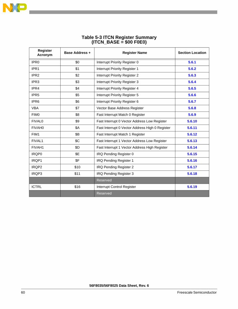
56F8035/56F8025 Data Sheet, Rev. 6
60 Freescale Semiconductor
Table 5-3 ITCN Register Summary(ITCN_BASE = $00 F0E0)
Register Acronym Base Address + Register Name Section Location
IPR0 $0 Interrupt Priority Register 0 5.6.1
IPR1 $1 Interrupt Priority Register 1 5.6.2
IPR2 $2 Interrupt Priority Register 2 5.6.3
IPR3 $3 Interrupt Priority Register 3 5.6.4
IPR4 $4 Interrupt Priority Register 4 5.6.5
IPR5 $5 Interrupt Priority Register 5 5.6.6
IPR6 $6 Interrupt Priority Register 6 5.6.7
VBA $7 Vector Base Address Register 5.6.8
FIM0 $8 Fast Interrupt Match 0 Register 5.6.9
FIVAL0 $9 Fast Interrupt 0 Vector Address Low Register 5.6.10
FIVAH0 $A Fast Interrupt 0 Vector Address High 0 Register 5.6.11
FIM1 $B Fast Interrupt Match 1 Register 5.6.12
FIVAL1 $C Fast Interrupt 1 Vector Address Low Register 5.6.13
FIVAH1 $D Fast Interrupt 1 Vector Address High Register 5.6.14
IRQP0 $E IRQ Pending Register 0 5.6.15
IRQP1 $F IRQ Pending Register 1 5.6.16
IRQP2 $10 IRQ Pending Register 2 5.6.17
IRQP3 $11 IRQ Pending Register 3 5.6.18
Reserved
ICTRL $16 Interrupt Control Register 5.6.19
Reserved

Register Descriptions
56F8035/56F8025 Data Sheet, Rev. 6
Freescale Semiconductor 61
Figure 5-2 ITCN Register Map Summary
Add. Offset
Register Name 15 14 13 12 11 10 9 8 7 6 5 4 3 2 1 0
$0 IPR0R
PLL IPL LVI IPL0 0
RX_REG IPL TX_REG IPL TRBUF IPL BKPT_U IPL STPCNT IPLW
$1 IPR1R
GPIOD IPL0 0 0 0 0 0 0 0
FM_CBE IPL FM_CC IPL FM_ERR IPLW
$2 IPR2R QSCI0_XMIT
IPL0 0 0 0 QSPI0_XMIT
IPL QSPI0_RCV
IPL GPIOA IPL GPIOB IPL GPIOC IPLW
$3 IPR3R
I2C_ERR IPL0 0 0 0 0 0 0 0 QSCI0_RCV
IPLQSCI0_RERR
IPLQSCI0_TIDL
IPLW
$4 IPR4R
TMRA_3 IPL TMRA_2 IPL TMRA_1 IPL TMRA_0 IPL I2C_STAT IPL I2C_TX IPL I2C_RX IPL I2C_GEN IPL
W
$5 IPR5R
PIT1 IPL PIT0 IPL COMPB IPL COMPA IPL TMRB_3 IPL TMRB_2 IPL TMRB_1 IPL TMRB_0 IPLW
$6 IPR60 0 0 0
PWM_F IPL PWM_RL IPL ADC_ZC IPL ADCB_CC IPL ADCA_CC IPL PIT2 IPL
$7 VBAR 0 0
VECTOR_BASE_ADDRESSW
$8 FIM0R 0 0 0 0 0 0 0 0 0 0
FAST INTERRUPT 0W
$9 FIVAL0R
FAST INTERRUPT 0 VECTOR ADDRESS LOWW
$A FIVAH0R 0 0 0 0 0 0 0 0 0 0 0 FAST INTERRUPT 0 VECTOR
ADDRESS HIGHW
$B FIM1R 0 0 0 0 0 0 0 0 0 0
FAST INTERRUPT 1W
$C FIVAL1R
FAST INTERRUPT 1 VECTOR ADDRESS LOWW
$D FIVAH1R 0 0 0 0 0 0 0 0 0 0 0 FAST INTERRUPT 1 VECTOR
ADDRESS HIGHW
$E IRQP0R PENDING[16:2] 1W
$F IRQP1R PENDING[32:17]W
$10 IRQP2R PENDING[48:33]W
$11 IRQP3R PENDING[63:49]W
Reserved
$16 ICTRLR INT IPIC VAB INT_
DIS1 1 1 0 0
W
Reserved
= Reserved

56F8035/56F8025 Data Sheet, Rev. 6
62 Freescale Semiconductor
5.6.1 Interrupt Priority Register 0 (IPR0)
Figure 5-3 Interrupt Priority Register 0 (IPR0)
5.6.1.1 PLL Loss of Reference or Change in Lock Status Interrupt Priority Level (PLL IPL)—Bits 15–14
This field is used to set the interrupt priority levels for the PLL Loss of Reference or Change in Lock StatusIRQ. This IRQ is limited to priorities 1 through 3. It is disabled by default.
• 00 = IRQ disabled (default)• 01 = IRQ is priority level 1• 10 = IRQ is priority level 2• 11 = IRQ is priority level 3
5.6.1.2 Low Voltage Detector Interrupt Priority Level (LVI IPL)—Bits 13–12This field is used to set the interrupt priority levels for the Low Voltage Detector IRQ. This IRQ is limitedto priorities 1 through 3 and is disabled by default.
• 00 = IRQ disabled (default)• 01 = IRQ is priority level 1• 10 = IRQ is priority level 2• 11 = IRQ is priority level 3
5.6.1.3 Reserved—Bits 11–10This bit field is reserved. Each bit must be set to 0.
5.6.1.4 EOnCE Receive Register Full Interrupt Priority Level (RX_REG IPL)— Bits 9–8
This field is used to set the interrupt priority level for the EOnCE Receive Register Full IRQ. This IRQ islimited to priorities 1 through 3. It is disabled by default.
• 00 = IRQ disabled (default)• 01 = IRQ is priority level 1• 10 = IRQ is priority level 2• 11 = IRQ is priority level 3
Base + $0 15 14 13 12 11 10 9 8 7 6 5 4 3 2 1 0Read
PLL IPL LVI IPL0 0
RX_REG IPL TX_REG IPL TRBUF IPL BKPT_U IPL STPCNT IPLWrite
RESET 0 0 0 0 0 0 0 0 0 0 0 0 0 0 0 0

Register Descriptions
56F8035/56F8025 Data Sheet, Rev. 6
Freescale Semiconductor 63
5.6.1.5 EOnCE Transmit Register Empty Interrupt Priority Level (TX_REG IPL)— Bits 7–6
This field is used to set the interrupt priority level for the EOnCE Transmit Register Empty IRQ. This IRQis limited to priorities 1 through 3. It is disabled by default.
• 00 = IRQ disabled (default)• 01 = IRQ is priority level 1• 10 = IRQ is priority level 2• 11 = IRQ is priority level 3
5.6.1.6 EOnCE Trace Buffer Interrupt Priority Level (TRBUF IPL)— Bits 5–4
This field is used to set the interrupt priority level for the EOnCE Trace Buffer IRQ. This IRQ is limitedto priorities 1 through 3. It is disabled by default.
• 00 = IRQ disabled (default)• 01 = IRQ is priority level 1• 10 = IRQ is priority level 2• 11 = IRQ is priority level 3
5.6.1.7 EOnCE Breakpoint Unit Interrupt Priority Level (BKPT_U IPL)— Bits 3–2
This field is used to set the interrupt priority level for the EOnCE Breakpoint Unit IRQ. This IRQ is limitedto priorities 1 through 3. It is disabled by default.
• 00 = IRQ disabled (default)• 01 = IRQ is priority level 1• 10 = IRQ is priority level 2• 11 = IRQ is priority level 3
5.6.1.8 EOnCE Step Counter Interrupt Priority Level (STPCNT IPL)— Bits 1–0
This field is used to set the interrupt priority level for the EOnCE Step Counter IRQ. This IRQ is limitedto priorities 1 through 3. It is disabled by default.
• 00 = IRQ disabled (default)• 01 = IRQ is priority level 1• 10 = IRQ is priority level 2• 11 = IRQ is priority level 3

56F8035/56F8025 Data Sheet, Rev. 6
64 Freescale Semiconductor
5.6.2 Interrupt Priority Register 1 (IPR1)
Figure 5-4 Interrupt Priority Register 1 (IPR1)
5.6.2.1 GPIOD Interrupt Priority Level (GPIOD IPL)—Bits 15–14This field is used to set the interrupt priority level for the GPIOD IRQ. This IRQ is limited to priorities 0through 2. It is disabled by default.
• 00 = IRQ disabled (default)• 01 = IRQ is priority level 0• 10 = IRQ is priority level 1• 11 = IRQ is priority level 2
5.6.2.2 Reserved—Bits 13–6This bit field is reserved. Each bit must be set to 0.
5.6.2.3 FM Command, Data, Address Buffers Empty Interrupt Priority Level (FM_CBE IPL)—Bits 5–4
This field is used to set the interrupt priority level for the FM Command, Data Address Buffers EmptyIRQ. This IRQ is limited to priorities 0 through 2. It is disabled by default.
• 00 = IRQ disabled (default)• 01 = IRQ is priority level 0• 10 = IRQ is priority level 1• 11 = IRQ is priority level 2
5.6.2.4 FM Command Complete Interrupt Priority Level (FM_CC IPL)—Bits 3–2This field is used to set the interrupt priority level for the FM Command Complete IRQ. This IRQ islimited to priorities 0 through 2. It is disabled by default.
• 00 = IRQ disabled (default)• 01 = IRQ is priority level 0• 10 = IRQ is priority level 1• 11 = IRQ is priority level 2
Base + $1 15 14 13 12 11 10 9 8 7 6 5 4 3 2 1 0Read
GPIOD IPL0 0 0 0 0 0 0 0
FM_CBE IPL FM_CC IPL FM_ERR IPLWrite
RESET 0 0 0 0 0 0 0 0 0 0 0 0 0 0 0 0

Register Descriptions
56F8035/56F8025 Data Sheet, Rev. 6
Freescale Semiconductor 65
5.6.2.5 FM Error Interrupt Priority Level (FM_ERR IPL)—Bits 1–0This field is used to set the interrupt priority level for the FM Error IRQ. This IRQ is limited to priorities0 through 2. It is disabled by default.
• 00 = IRQ disabled (default)• 01 = IRQ is priority level 0• 10 = IRQ is priority level 1• 11 = IRQ is priority level 2
5.6.3 Interrupt Priority Register 2 (IPR2)
Figure 5-5 Interrupt Priority Register 2 (IPR2)
5.6.3.1 QSCI 0 Transmitter Empty Interrupt Priority Level (QSCI0_XMIT IPL)—Bits 15–14
This field is used to set the interrupt priority level for the QSCI0 Transmitter Empty IRQ. This IRQ islimited to priorities 0 through 2. It is disabled by default.
• 00 = IRQ disabled (default)• 01 = IRQ is priority level 0• 10 = IRQ is priority level 1• 11 = IRQ is priority level 2
5.6.3.2 Reserved—Bits 13–10This bit field is reserved. Each bit must be set to 0.
5.6.3.3 QSPI 0 Transmitter Empty Interrupt Priority Level (QSPI0_XMIT IPL)—Bits 9–8
This field is used to set the interrupt priority level for the QSPI0 Transmitter Empty IRQ. This IRQ islimited to priorities 0 through 2. It is disabled by default.
• 00 = IRQ disabled (default)• 01 = IRQ is priority level 0• 10 = IRQ is priority level 1• 11 = IRQ is priority level 2
Base + $2 15 14 13 12 11 10 9 8 7 6 5 4 3 2 1 0Read QSCI0_XMIT
IPL0 0 0 0 QSPI0_XMIT
IPL QSPI0_RCV
IPL GPIOA IPL GPIOB IPL GPIOC IPLWrite
RESET 0 0 0 0 0 0 0 0 0 0 0 0 0 0 0 0

56F8035/56F8025 Data Sheet, Rev. 6
66 Freescale Semiconductor
5.6.3.4 QSPI 0 Receiver Full Interrupt Priority Level (QSPI0_RCV IPL)—Bits 7–6This field is used to set the interrupt priority level for the QSPI0 Receiver Full IRQ. This IRQ is limitedto priorities 0 through 2. It is disabled by default.
• 00 = IRQ disabled (default)• 01 = IRQ is priority level 0• 10 = IRQ is priority level 1• 11 = IRQ is priority level 2
5.6.3.5 GPIOA Interrupt Priority Level (GPIOA IPL)—Bits 5–4This field is used to set the interrupt priority level for the GPIOA IRQ. This IRQ is limited to priorities 0through 2. It is disabled by default.
• 00 = IRQ disabled (default)• 01 = IRQ is priority level 0• 10 = IRQ is priority level 1• 11 = IRQ is priority level 2
5.6.3.6 GPIOB Interrupt Priority Level (GPIOB IPL)—Bits 3–2This field is used to set the interrupt priority level for the GPIOB IRQ. This IRQ is limited to priorities 0through 2. It is disabled by default.
• 00 = IRQ disabled (default)• 01 = IRQ is priority level 0• 10 = IRQ is priority level 1• 11 = IRQ is priority level 2
5.6.3.7 GPIOC Interrupt Priority Level (GPIOC IPL)—Bits 1–0This field is used to set the interrupt priority level for the GPIOC IRQ. This IRQ is limited to priorities 0through 2. It is disabled by default.
• 00 = IRQ disabled (default)• 01 = IRQ is priority level 0• 10 = IRQ is priority level 1• 11 = IRQ is priority level 2
5.6.4 Interrupt Priority Register 3 (IPR3)
Figure 5-6 Interrupt Priority Register 3 (IPR3)
Base + $3 15 14 13 12 11 10 9 8 7 6 5 4 3 2 1 0Read
I2C_ERR IPL0 0 0 0 0 0 0 0 QSCI0_RCV
IPLQSCI0_RERR
IPLQSCI0_TIDL
IPLWriteRESET 0 0 0 0 0 0 0 0 0 0 0 0 0 0 0 0

Register Descriptions
56F8035/56F8025 Data Sheet, Rev. 6
Freescale Semiconductor 67
5.6.4.1 I2C Error Interrupt Priority Level (I2C_ERR IPL)—Bits 15–14This field is used to set the interrupt priority level for the I2C Error IRQ. This IRQ is limited to priorities0 through 2. It is disabled by default.
• 00 = IRQ disabled (default)• 01 = IRQ is priority level 0• 10 = IRQ is priority level 1• 11 = IRQ is priority level 2
5.6.4.2 Reserved—Bits 13–6This bit field is reserved. Each bit must be set to 0.
5.6.4.3 QSCI 0 Receiver Full Interrupt Priority Level (QSCI0_RCV IPL)—Bits 5–4This field is used to set the interrupt priority level for the QSCI0 Receiver Full IRQ. This IRQ is limitedto priorities 0 through 2. It is disabled by default.
• 00 = IRQ disabled (default)• 01 = IRQ is priority level 0• 10 = IRQ is priority level 1• 11 = IRQ is priority level 2
5.6.4.4 QSCI 0 Receiver Error Interrupt Priority Level (QSCI0_RERR IPL)—Bits 3–2
This field is used to set the interrupt priority level for the QSCI0 Receiver Error IRQ. This IRQ is limitedto priorities 0 through 2. It is disabled by default.
• 00 = IRQ disabled (default)• 01 = IRQ is priority level 0• 10 = IRQ is priority level 1• 11 = IRQ is priority level 2
5.6.4.5 QSCI 0 Transmitter Idle Interrupt Priority Level (QSCI0_TIDL IPL)—Bits 1–0
This field is used to set the interrupt priority level for the QSCI0 Transmitter Idle IRQ. This IRQ is limitedto priorities 0 through 2. It is disabled by default.
• 00 = IRQ disabled (default)• 01 = IRQ is priority level 0• 10 = IRQ is priority level 1• 11 = IRQ is priority level 2

56F8035/56F8025 Data Sheet, Rev. 6
68 Freescale Semiconductor
5.6.5 Interrupt Priority Register 4 (IPR4)
Figure 5-7 Interrupt Priority Register 4 (IPR4)
5.6.5.1 Timer A, Channel 3 Interrupt Priority Level (TMRA_3 IPL)—Bits 15–14
This field is used to set the interrupt priority level for the Timer A, Channel 3 IRQ. This IRQ is limited topriorities 0 through 2. It is disabled by default.
• 00 = IRQ disabled (default)• 01 = IRQ is priority level 0• 10 = IRQ is priority level 1• 11 = IRQ is priority level 2
5.6.5.2 Timer A, Channel 2 Interrupt Priority Level (TMRA_2 IPL)—Bits 13–12
This field is used to set the interrupt priority level for the Timer A, Channel 2 IRQ. This IRQ is limited topriorities 0 through 2. It is disabled by default.
• 00 = IRQ disabled (default)• 01 = IRQ is priority level 0• 10 = IRQ is priority level 1• 11 = IRQ is priority level 2
5.6.5.3 Timer A, Channel 1 Interrupt Priority Level (TMRA_1 IPL)—Bits 11–10
This field is used to set the interrupt priority level for the Timer A, Channel 1 IRQ. This IRQ is limited topriorities 0 through 2. It is disabled by default.
• 00 = IRQ disabled (default)• 01 = IRQ is priority level 0• 10 = IRQ is priority level 1• 11 = IRQ is priority level 2
Base + $4 15 14 13 12 11 10 9 8 7 6 5 4 3 2 1 0Read
TMRA_3 IPL TMRA_2 IPL TMRA_1 IPL TMRA_0 IPL I2C_STAT IPL I2C_TX IPL I2C_RX IPL I2C_GEN IPLWrite
RESET 0 0 0 0 0 0 0 0 0 0 0 0 0 0 0 0
Register Descriptions
56F8035/56F8025 Data Sheet, Rev. 6
Freescale Semiconductor 69
5.6.5.4 Timer A, Channel 0 Interrupt Priority Level (TMRA_0 IPL)—Bits 9–8
This field is used to set the interrupt priority level for the Timer A, Channel 0 IRQ. This IRQ is limited topriorities 0 through 2. It is disabled by default.
• 00 = IRQ disabled (default)• 01 = IRQ is priority level 0• 10 = IRQ is priority level 1• 11 = IRQ is priority level 2
5.6.5.5 I2C Status Interrupt Priority Level (I2C_STAT IPL)—Bits 7–6This field is used to set the interrupt priority level for the I2C Status IRQ. This IRQ is limited to priorities0 through 2. It is disabled by default.
• 00 = IRQ disabled (default)• 01 = IRQ is priority level 0• 10 = IRQ is priority level 1• 11 = IRQ is priority level 2
5.6.5.6 I2C Transmit Interrupt Priority Level (I2C_TX IPL)—Bits 5–4This field is used to set the interrupt priority level for the I2C Transmit IRQ. This IRQ is limited topriorities 0 through 2. It is disabled by default.
• 00 = IRQ disabled (default)• 01 = IRQ is priority level 0• 10 = IRQ is priority level 1• 11 = IRQ is priority level 2
5.6.5.7 I2C Receive Interrupt Priority Level (I2C_RX IPL)— Bits 3–2This field is used to set the interrupt priority level for the I2C Receiver IRQ. This IRQ is limited topriorities 0 through 2. It is disabled by default.
• 00 = IRQ disabled (default)• 01 = IRQ is priority level 0• 10 = IRQ is priority level 1• 11 = IRQ is priority level 2
5.6.5.8 I2C General Call Interrupt Priority Level (I2C_GEN IPL)—Bits 1–0This field is used to set the interrupt priority level for the I2C General Call IRQ. This IRQ is limited topriorities 0 through 2. It is disabled by default.
• 00 = IRQ disabled (default)• 01 = IRQ is priority level 0
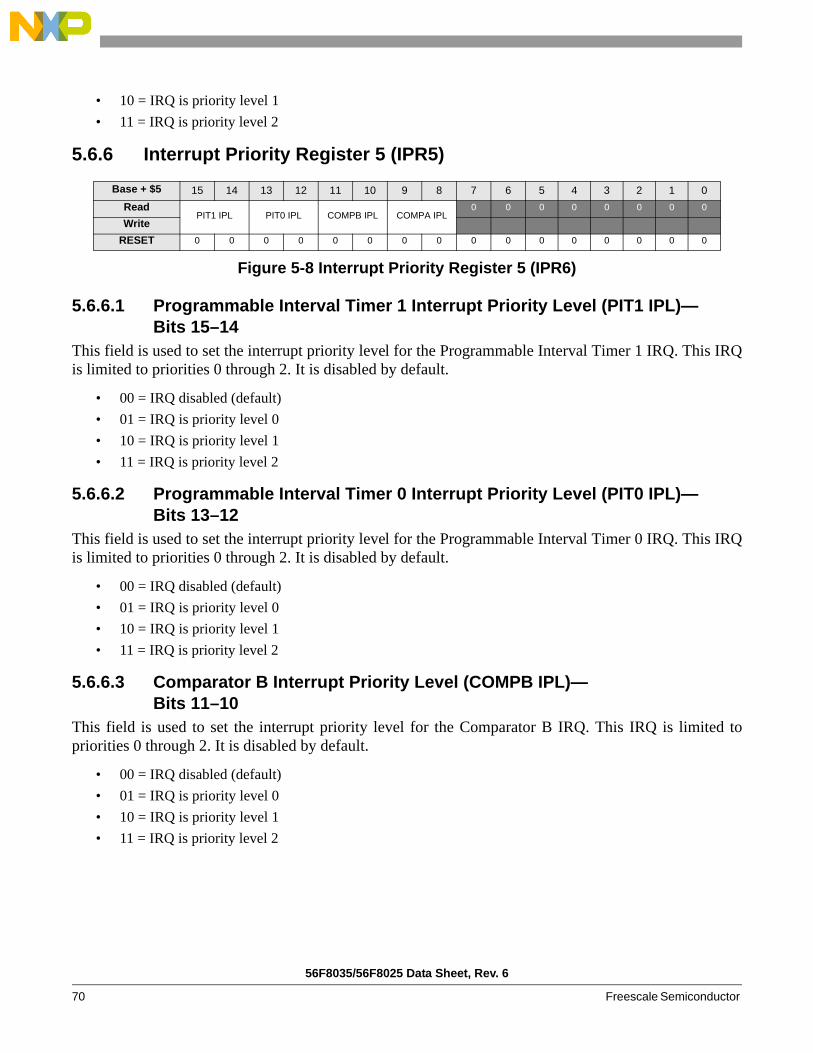
56F8035/56F8025 Data Sheet, Rev. 6
70 Freescale Semiconductor
• 10 = IRQ is priority level 1• 11 = IRQ is priority level 2
5.6.6 Interrupt Priority Register 5 (IPR5)
Figure 5-8 Interrupt Priority Register 5 (IPR6)
5.6.6.1 Programmable Interval Timer 1 Interrupt Priority Level (PIT1 IPL)—Bits 15–14
This field is used to set the interrupt priority level for the Programmable Interval Timer 1 IRQ. This IRQis limited to priorities 0 through 2. It is disabled by default.
• 00 = IRQ disabled (default)• 01 = IRQ is priority level 0• 10 = IRQ is priority level 1• 11 = IRQ is priority level 2
5.6.6.2 Programmable Interval Timer 0 Interrupt Priority Level (PIT0 IPL)—Bits 13–12
This field is used to set the interrupt priority level for the Programmable Interval Timer 0 IRQ. This IRQis limited to priorities 0 through 2. It is disabled by default.
• 00 = IRQ disabled (default)• 01 = IRQ is priority level 0• 10 = IRQ is priority level 1• 11 = IRQ is priority level 2
5.6.6.3 Comparator B Interrupt Priority Level (COMPB IPL)—Bits 11–10
This field is used to set the interrupt priority level for the Comparator B IRQ. This IRQ is limited topriorities 0 through 2. It is disabled by default.
• 00 = IRQ disabled (default)• 01 = IRQ is priority level 0• 10 = IRQ is priority level 1• 11 = IRQ is priority level 2
Base + $5 15 14 13 12 11 10 9 8 7 6 5 4 3 2 1 0Read
PIT1 IPL PIT0 IPL COMPB IPL COMPA IPL0 0 0 0 0 0 0 0
WriteRESET 0 0 0 0 0 0 0 0 0 0 0 0 0 0 0 0
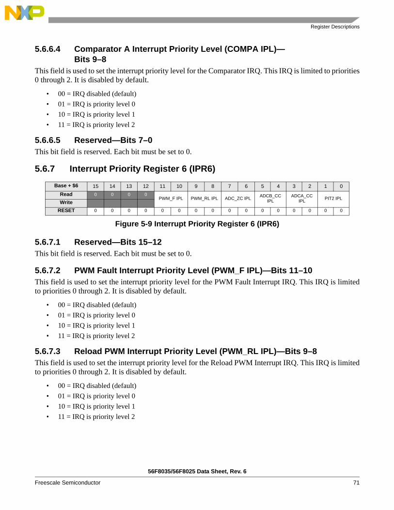
Register Descriptions
56F8035/56F8025 Data Sheet, Rev. 6
Freescale Semiconductor 71
5.6.6.4 Comparator A Interrupt Priority Level (COMPA IPL)—Bits 9–8
This field is used to set the interrupt priority level for the Comparator IRQ. This IRQ is limited to priorities0 through 2. It is disabled by default.
• 00 = IRQ disabled (default)• 01 = IRQ is priority level 0• 10 = IRQ is priority level 1• 11 = IRQ is priority level 2
5.6.6.5 Reserved—Bits 7–0This bit field is reserved. Each bit must be set to 0.
5.6.7 Interrupt Priority Register 6 (IPR6)
Figure 5-9 Interrupt Priority Register 6 (IPR6)
5.6.7.1 Reserved—Bits 15–12 This bit field is reserved. Each bit must be set to 0.
5.6.7.2 PWM Fault Interrupt Priority Level (PWM_F IPL)—Bits 11–10This field is used to set the interrupt priority level for the PWM Fault Interrupt IRQ. This IRQ is limitedto priorities 0 through 2. It is disabled by default.
• 00 = IRQ disabled (default)• 01 = IRQ is priority level 0• 10 = IRQ is priority level 1• 11 = IRQ is priority level 2
5.6.7.3 Reload PWM Interrupt Priority Level (PWM_RL IPL)—Bits 9–8This field is used to set the interrupt priority level for the Reload PWM Interrupt IRQ. This IRQ is limitedto priorities 0 through 2. It is disabled by default.
• 00 = IRQ disabled (default)• 01 = IRQ is priority level 0• 10 = IRQ is priority level 1• 11 = IRQ is priority level 2
Base + $6 15 14 13 12 11 10 9 8 7 6 5 4 3 2 1 0Read 0 0 0 0
PWM_F IPL PWM_RL IPL ADC_ZC IPL ADCB_CC IPL
ADCA_CC IPL PIT2 IPL
WriteRESET 0 0 0 0 0 0 0 0 0 0 0 0 0 0 0 0

56F8035/56F8025 Data Sheet, Rev. 6
72 Freescale Semiconductor
5.6.7.4 ADC Zero Crossing Interrupt Priority Level (ADC_ZC IPL)—Bits 7–6This field is used to set the interrupt priority level for the ADC Zero Crossing IRQ. This IRQ is limited topriorities 0 through 2. It is disabled by default.
• 00 = IRQ disabled (default)• 01 = IRQ is priority level 0• 10 = IRQ is priority level 1• 11 = IRQ is priority level 2
5.6.7.5 ADC B Conversion Complete Interrupt Priority Level (ADCB_CC IPL)—Bits 5–4
This field is used to set the interrupt priority level for the ADC B Conversion Complete IRQ. This IRQ islimited to priorities 0 through 2. It is disabled by default.
• 00 = IRQ disabled (default)• 01 = IRQ is priority level 0• 10 = IRQ is priority level 1• 11 = IRQ is priority level 2
5.6.7.6 ADC A Conversion Complete Interrupt Priority Level (ADCA_CC IPL)—Bits 3–2
This field is used to set the interrupt priority level for the ADC A Conversion Complete IRQ. This IRQ islimited to priorities 0 through 2. It is disabled by default.
• 00 = IRQ disabled (default)• 01 = IRQ is priority level 0• 10 = IRQ is priority level 1• 11 = IRQ is priority level 2
5.6.7.7 Programmable Interval Timer 2 Interrupt Priority Level (PIT2 IPL)—Bits 1–0
This field is used to set the interrupt priority level for the Programmable Interval Timer 2 IRQ. This IRQis limited to priorities 0 through 2. It is disabled by default.
• 00 = IRQ disabled (default)• 01 = IRQ is priority level 0• 10 = IRQ is priority level 1• 11 = IRQ is priority level 2

Register Descriptions
56F8035/56F8025 Data Sheet, Rev. 6
Freescale Semiconductor 73
5.6.8 Vector Base Address Register (VBA)
Figure 5-10 Vector Base Address Register (VBA)
5.6.8.1 Reserved—Bits 15–14 This bit field is reserved. Each bit must be set to 0.
5.6.8.2 Vector Address Bus (VAB) Bits 13–0The value in this register is used as the upper 14 bits of the interrupt vector VAB[20:0]. The lower 7 bitsare determined based on the highest priority interrupt and are then appended onto VBA before presentingthe full VAB to the Core.
5.6.9 Fast Interrupt Match 0 Register (FIM0)
Figure 5-11 Fast Interrupt Match 0 Register (FIM0)
5.6.9.1 Reserved—Bits 15–6 This bit field is reserved. Each bit must be set to 0.
5.6.9.2 Fast Interrupt 0 Vector Number (FAST INTERRUPT 0)—Bits 5–0These values determine which IRQ will be Fast Interrupt 0. Fast Interrupts vector directly to a serviceroutine based on values in the Fast Interrupt Vector Address registers without having to go to a jump tablefirst. IRQs used as Fast Interrupts must be set to priority level 2. Unexpected results will occur if a FastInterrupt vector is set to any other priority. A Fast Interrupt automatically becomes the highest-prioritylevel 2 interrupt regardless of its location in the interrupt table prior to being declared as Fast Interrupt.Fast Interrupt 0 has priority over Fast Interrupt 1. To determine the vector number of each IRQ, refer tothe vector table.
Base + $7 15 14 13 12 11 10 9 8 7 6 5 4 3 2 1 0Read 0 0
VECTOR_BASE_ADDRESSWrite
RESET1
1. The 56F8035 resets to a value of 0 x 0000. This corresponds to reset addresses of 0 x 000000.The 56F8025 resets to a value of 0 x 0080. This corresponds to reset addresses of 0 x 004000.
0 0 0 0 0 0 0 0 1 0 0 0 0 0 0 0
Base + $8 15 14 13 12 11 10 9 8 7 6 5 4 3 2 1 0Read 0 0 0 0 0 0 0 0 0 0
FAST INTERRUPT 0Write
RESET 0 0 0 0 0 0 0 0 0 0 0 0 0 0 0 0

56F8035/56F8025 Data Sheet, Rev. 6
74 Freescale Semiconductor
5.6.10 Fast Interrupt 0 Vector Address Low Register (FIVAL0)
Figure 5-12 Fast Interrupt 0 Vector Address Low Register (FIVAL0)
5.6.10.1 Fast Interrupt 0 Vector Address Low (FIVAL0)—Bits 15–0The lower 16 bits of the vector address used for Fast Interrupt 0. This register is combined with FIVAH0to form the 21-bit vector address for Fast Interrupt 0 defined in the FIM0 register.
5.6.11 Fast Interrupt 0 Vector Address High Register (FIVAH0)
Figure 5-13 Fast Interrupt 0 Vector Address High Register (FIVAH0)
5.6.11.1 Reserved—Bits 15–5This bit field is reserved. Each bit must be set to 0.
5.6.11.2 Fast Interrupt 0 Vector Address High (FIVAH0)—Bits 4–0The upper five bits of the vector address used for Fast Interrupt 0. This register is combined with FIVAL0to form the 21-bit vector address for Fast Interrupt 0 defined in the FIM0 register.
5.6.12 Fast Interrupt 1 Match Register (FIM1)
Figure 5-14 Fast Interrupt 1 Match Register (FIM1)
5.6.12.1 Reserved—Bits 15–6This bit field is reserved. Each bit must be set to 0.
5.6.12.2 Fast Interrupt 1 Vector Number (FAST INTERRUPT 1)—Bits 5–0 These values determine which IRQ will be Fast Interrupt 1. Fast Interrupts vector directly to a serviceroutine based on values in the Fast Interrupt Vector Address registers without having to go to a jump tablefirst. IRQs used as Fast Interrupts must be set to priority level 2. Unexpected results will occur if a Fast
Base + $9 15 14 13 12 11 10 9 8 7 6 5 4 3 2 1 0Read
FAST INTERRUPT 0 VECTOR ADDRESS LOWWrite
RESET 0 0 0 0 0 0 0 0 0 0 0 0 0 0 0 0
Base + $A 15 14 13 12 11 10 9 8 7 6 5 4 3 2 1 0Read 0 0 0 0 0 0 0 0 0 0 0 FAST INTERRUPT 0 VECTOR
ADDRESS HIGHWriteRESET 0 0 0 0 0 0 0 0 0 0 0 0 0 0 0 0
Base + $B 15 14 13 12 11 10 9 8 7 6 5 4 3 2 1 0Read 0 0 0 0 0 0 0 0 0 0
FAST INTERRUPT 1Write
RESET 0 0 0 0 0 0 0 0 0 0 0 0 0 0 0 0

Register Descriptions
56F8035/56F8025 Data Sheet, Rev. 6
Freescale Semiconductor 75
Interrupt vector is set to any other priority. A Fast Interrupt automatically becomes the highest prioritylevel 2 interrupt, regardless of its location in the interrupt table prior to being declared as Fast Interrupt.Fast Interrupt 0 has priority over Fast Interrupt 1. To determine the vector number of each IRQ, refer tothe vector table.
5.6.13 Fast Interrupt 1 Vector Address Low Register (FIVAL1)
Figure 5-15 Fast Interrupt 1 Vector Address Low Register (FIVAL1)
5.6.13.1 Fast Interrupt 1 Vector Address Low (FIVAL1)—Bits 15–0The lower 16 bits of the vector address used for Fast Interrupt 1. This register is combined with FIVAH1to form the 21-bit vector address for Fast Interrupt 1 defined in the FIM1 register.
5.6.14 Fast Interrupt 1 Vector Address High (FIVAH1)
Figure 5-16 Fast Interrupt 1 Vector Address High Register (FIVAH1)
5.6.14.1 Reserved—Bits 15–5This bit field is reserved. Each bit must be set to 0.
5.6.14.2 Fast Interrupt 1 Vector Address High (FIVAH1)—Bits 4–0The upper five bits of the vector address used for Fast Interrupt 1. This register is combined with FIVAL1to form the 21-bit vector address for Fast Interrupt 1 defined in the FIM1 register.
5.6.15 IRQ Pending Register 0 (IRQP0)
Figure 5-17 IRQ Pending Register 0 (IRQP0)
Base + $C 15 14 13 12 11 10 9 8 7 6 5 4 3 2 1 0Read
FAST INTERRUPT 1 VECTOR ADDRESS LOW Write
RESET 0 0 0 0 0 0 0 0 0 0 0 0 0 0 0 0
Base + $D 15 14 13 12 11 10 9 8 7 6 5 4 3 2 1 0Read 0 0 0 0 0 0 0 0 0 0 0 FAST INTERRUPT 1 VECTOR
ADDRESS HIGHWriteRESET 0 0 0 0 0 0 0 0 0 0 0 0 0 0 0 0
Base + $E 15 14 13 12 11 10 9 8 7 6 5 4 3 2 1 0Read PENDING[16:2] 1
WriteRESET 1 1 1 1 1 1 1 1 1 1 1 1 1 1 1 1

56F8035/56F8025 Data Sheet, Rev. 6
76 Freescale Semiconductor
5.6.15.1 IRQ Pending (PENDING)—Bits 16–2These register bit values represent the pending IRQs for interrupt vector numbers 2 through 16. AscendingIRQ numbers correspond to ascending bit locations.
• 0 = IRQ pending for this vector number• 1 = No IRQ pending for this vector number
5.6.15.2 Reserved—Bit 0This bit field is reserved. It must be set to 1.
5.6.16 IRQ Pending Register 1 (IRQP1)
Figure 5-18 IRQ Pending Register 1 (IRQP1)
5.6.16.1 IRQ Pending (PENDING)—Bits 32–17These register bit values represent the pending IRQs for interrupt vector numbers 17 through 32.Ascending IRQ numbers correspond to ascending bit locations.
• 0 = IRQ pending for this vector number• 1 = No IRQ pending for this vector number
5.6.17 IRQ Pending Register 2 (IRQP2)
Figure 5-19 IRQ Pending Register 2 (IRQP2)
5.6.17.1 IRQ Pending (PENDING)—Bits 48–33These register bit values represent the pending IRQs for interrupt vector numbers 33 through 48.Ascending IRQ numbers correspond to ascending bit locations.
• 0 = IRQ pending for this vector number• 1 = No IRQ pending for this vector number
Base + $F 15 14 13 12 11 10 9 8 7 6 5 4 3 2 1 0Read PENDING[32:17]
WriteRESET 1 1 1 1 1 1 1 1 1 1 1 1 1 1 1 1
Base + $10 15 14 13 12 11 10 9 8 7 6 5 4 3 2 1 0Read PENDING[48:33]
WriteRESET 1 1 1 1 1 1 1 1 1 1 1 1 1 1 1 1

Register Descriptions
56F8035/56F8025 Data Sheet, Rev. 6
Freescale Semiconductor 77
5.6.18 IRQ Pending Register 3 (IRQP3)
Figure 5-20 IRQ Pending Register 3 (IRQP3)
5.6.18.1 IRQ Pending (PENDING)—Bits 63–49These register bit values represent the pending IRQs for interrupt vector numbers 49 through 63.Ascending IRQ numbers correspond to ascending bit locations.
• 0 = IRQ pending for this vector number• 1 = No IRQ pending for this vector number
5.6.19 Interrupt Control Register (ICTRL)
Figure 5-21 Interrupt Control Register (ICTRL)
5.6.19.1 Interrupt (INT)—Bit 15This read-only bit reflects the state of the interrupt to the 56800E core.
• 0 = No interrupt is being sent to the 56800E core• 1 = An interrupt is being sent to the 56800E core
5.6.19.2 Interrupt Priority Level (IPIC)—Bits 14–13These read-only bits reflect the state of the new interrupt priority level bits being presented to the 56800Ecore. These bits indicate the priority level needed for a new IRQ to interrupt the current interrupt beingsent to the 56800E core. This field is only updated when the 56800E core jumps to a new interrupt serviceroutine.
Note: Nested interrupts may cause this field to be updated before the original interrupt service routine can read it.
• 00 = Required nested exception priority levels are 0, 1, 2, or 3• 01 = Required nested exception priority levels are 1, 2, or 3• 10 = Required nested exception priority levels are 2 or 3• 11 = Required nested exception priority level is 3
Base + $11 15 14 13 12 11 10 9 8 7 6 5 4 3 2 1 0Read PENDING[63:49]
WriteRESET 1 1 1 1 1 1 1 1 1 1 1 1 1 1 1 1
$Base + $16 15 14 13 12 11 10 9 8 7 6 5 4 3 2 1 0Read INT IPIC VAB INT_
DIS1 1 1 0 0
WriteRESET 0 0 0 0 0 0 0 0 0 0 0 1 1 1 0 0

56F8035/56F8025 Data Sheet, Rev. 6
78 Freescale Semiconductor
5.6.19.3 Vector Number - Vector Address Bus (VAB)—Bits 12–6This read-only field shows bits [7:1] of the Vector Address Bus used at the time the last IRQ was taken.In the case of a Fast Interrupt, it shows the lower address bits of the jump address. This field is only updatedwhen the 56800E core jumps to a new interrupt service routine.
Note: Nested interrupts may cause this field to be updated before the original interrupt service routine can read it.
5.6.19.4 Interrupt Disable (INT_DIS)—Bit 5This bit allows all interrupts to be disabled.
• 0 = Normal operation (default)• 1 = All interrupts disabled
5.6.19.5 Reserved—Bits 4-2This bit field is reserved. Each bit must be set to 1.
5.6.19.6 Reserved—Bits 1–0This bit field is reserved. Each bit must be set to 0.
5.7 Resets
5.7.1 General
Table 5-4 Interrupt Priority Encoding
IPIC_VALUE[1:0] Current Interrupt Priority Level
Required Nested Exception Priority
00 No interrupt or SWILP Priorities 0, 1, 2, 3
01 Priority 0 Priorities 1, 2, 3
10 Priority 1 Priorities 2, 3
11 Priority 2 or 3 Priority 3
Table 5-5 Reset Summary
Reset Priority Source Characteristics
Core Reset RST Core reset from the SIM

Introduction
56F8035/56F8025 Data Sheet, Rev. 6
Freescale Semiconductor 79
5.7.2 Description of Reset Operation
5.7.2.1 Reset Handshake TimingThe ITCN provides the 56800E core with a reset vector address on the VAB pins whenever RESET isasserted from the SIM. The reset vector will be presented until the second rising clock edge after RESETis released. The general timing is shown in Figure 5-22.
Figure 5-22 Reset Interface
5.7.3 ITCN After ResetAfter reset, all of the ITCN registers are in their default states. This means all interrupts are disabled,except the core IRQs with fixed priorities:
• Illegal Instruction• SW Interrupt 3• HW Stack Overflow• Misaligned Long Word Access• SW Interrupt 2• SW Interrupt 1• SW Interrupt 0• SW Interrupt LP
These interrupts are enabled at their fixed priority levels.
Part 6 System Integration Module (SIM)
6.1 IntroductionThe SIM module is a system catchall for the glue logic that ties together the system-on-chip. It controlsdistribution of resets and clocks and provides a number of control features. The System IntegrationModule’s functions are discussed in more detail in the following sections.
RES
CLK
VAB
PAB
RESET_VECTOR_ADR
READ_ADR

56F8035/56F8025 Data Sheet, Rev. 6
80 Freescale Semiconductor
6.2 FeaturesThe SIM has the following features:
• Chip reset sequencing• Core and peripheral clock control and distribution• Stop/Wait mode control• System status control• Registers containing the JTAG ID of the chip• Controls for programmable peripheral and GPIO connections• Peripheral clocks for TMR and PWM with a high-speed (3X) option• Power-saving clock gating for peripherals• Three power modes (Run, Wait, Stop) to control power utilization
— Stop mode shuts down the 56800E core, system clock, and peripheral clock— Wait mode shuts down the 56800E core and unnecessary system clock operation— Run mode supports full device operation
• Controls the enable/disable functions of the 56800E core WAIT and STOP instructions with write protection capability
• Controls the enable/disable functions of Large Regulator Standby mode with write protection capability • Permits selected peripherals to run in Stop mode to generate Stop recovery interrupts• Controls for programmable peripheral and GPIO connections• Software chip reset• I/O short address base location control• Peripheral protection control to provide runaway code protection for safety-critical applications• Controls output of internal clock sources to CLKO pin• Four general-purpose software control registers are reset only at power-on• Peripherals Stop mode clocking control

Register Descriptions
56F8035/56F8025 Data Sheet, Rev. 6
Freescale Semiconductor 81
6.3 Register DescriptionsA write to an address without an associated register is an NOP. A read from an address without anassociated register returns unknown data.
Table 6-1 SIM Registers (SIM_BASE = $00 F100)
Register Acronym Base Address + Register Name Section
Location
CTRL $0 Control Register 6.3.1
RSTAT $1 Reset Status Register 6.3.2
SWC0 $2 Software Control Register 0 6.3.3
SWC1 $3 Software Control Register 1 6.3.3
SWC2 $4 Software Control Register 2 6.3.3
SWC3 $5 Software Control Register 3 6.3.3
MSHID $6 Most Significant Half of JTAG ID 6.3.4
LSHID $7 Least Significant Half of JTAG ID 6.3.5
PWR $8 Power Control Register 6.3.6
Reserved
CLKOUT $A CLKO Select Register 6.3.7
PCR $B Peripheral Clock Rate Register 6.3.8
PCE0 $C Peripheral Clock Enable Register 0 6.3.9
PCE1 $D Peripheral Clock Enable Register 0 6.3.10
SD0 $E Stop Disable Register 0 6.3.11
SD1 $F Stop Disable Register 1 6.3.12
IOSAHI $10 I/O Short Address Location High Register 6.3.13
IOSALO $11 I/O Short Address Location Low Register 6.3.14
PROT $12 Protection Register 6.3.15
GPSA0 $13 GPIO Peripheral Select Register 0 for GPIOA 6.3.16
GPSA1 $14 GPIO Peripheral Select Register 1 for GPIOA 6.3.17
GPSB0 $15 GPIO Peripheral Select Register 0 for GPIOB 6.3.18
GPSB1 $16 GPIO Peripheral Select Register 1 for GPIOB 6.3.19
GPSCD $17 GPIO Peripheral Select Register for GPIOC and GPIOD 6.3.20
IPS0 $18 Internal Peripheral Source Select Register 0 for PWM 6.3.21
IPS1 $19 Internal Peripheral Source Select Register 1 for DACs 6.3.22
IPS2 $1A Internal Peripheral Source Select Register 2 for Quad Timer A 6.3.23
Reserved

56F8035/56F8025 Data Sheet, Rev. 6
82 Freescale Semiconductor
Add. Offset
Address Acronym 15 14 13 12 11 10 9 8 7 6 5 4 3 2 1 0
$0 SIM_CTRL
R 0 0 0 0 0 0 0 0 0 0 ONCE EBL0
SW RST
STOP_DISABLE
WAIT_DISABLEW
$1 SIM_RSTAT
R 0 0 0 0 0 0 0 0 0 SWR COP_TOR
COP_LOR EXTR POR 0 0
W
$2 SIM_SWC0R
Software Control Data 0W
$3 SIM_SWC1R
Software Control Data 1W
$4 SIM_SWC2R
Software Control Data 2W
$5 SIM_SWC3R
Software Control Data 3W
$6 SIM_MSHIDR 0 0 0 0 0 0 0 1 1 1 1 1 0 0 1 0W
$7 SIM_LSHIDR 1 0 0 0 0 0 0 0 0 0 0 1 1 1 0 1W
$8 SIM_PWRR 0 0 0 0 0 0 0 0 0 0 0 0 0 0
LRSTDBYW
Reserved
$A SIM_CLKOUT
R 0 0 0 0 0 0PWM3 PWM2 PWM1 PWM0
1 0 0 0 0 0W
$B SIM_PCRR 0 TMRA_
CRPWM_
CRI2C_CR
0 0 0 0 0 0 0 0 0 0 0 0W
$C SIM_PCE0R
CMPB CMPA DAC1 DAC00
ADC0 0 0
I2C0
QSCI00
QSPI00
PWMW
$D SIM_PCE1R 0
PIT2 PIT1 PIT00 0 0 0 0 0 0 0
TA3 TA2 TA1 TA0W
$E SIM_SD0R CMPB_
SDCMPA_
SDDAC1_
SDDAC0_
SD0 ADC_
SD0 0 0 I2C_
SD0 QSCI0
_SD0 QSPI0
_SD0 PWM_
SDW
$F SIM_SD1R 0 PIT2_
SD PIT1_SD PIT0_SD
0 0 0 0 0 0 0 0 TA3_SD
TA2_SD
TA1_SD
TA0_SDW
$10 SIM_IOSAHIR 0 0 0 0 0 0 0 0 0 0 0 0 0 0
ISAL[23:22]W
$11 SIM_IOSALOR
ISAL[21:6]W
$12 SIM_PROTR 0 0 0 0 0 0 0 0 0 0 0 0
PCEP GIPSPW
$13 SIM_GPSA0R 0 0 0 GPS_
A6 GPS_A5 GPS_A40 0 0 0 0 0 0 0
W
$14 SIM_GPSA1R 0 0 0 0 0 0 0 0 0 GPS_
A110 GPS_
A10 GPS_A9 GPS_A8W
$15 SIM_GPSB0R 0
GPS_B6 GPS_B50 0 0
GPS_B3 GPS_B20 GPS_
B10 GPS_
B0W
$16 SIM_GPSB1R 0 0 0 0 0 0 0 GPS_
B110 GPS_
B100 0 0 0 0 GPS_
B7W
$17 SIM_GPSCDR 0 0 0 GPS_
D50 0 0 0 0 0 0 0 0 0 0 0
W
$18 SIM_IPS0R 0 0 IPS0_
FAULT20 IPS0_
FAULT10 0 0
IPS0_PSRC1 IPS0_PSRC0W
$19 SIM_IPS1R 0 0 0 0 0 0 0 0 0
IPS1_DSYNC10
IPS1_DSYNC0W
$1A SIM_IPS2R 0 0 0 IPS2_
TA30 0 0 IPS2_
TA20 0 0 IPS2_
TA10 0 0 0
W

Register Descriptions
56F8035/56F8025 Data Sheet, Rev. 6
Freescale Semiconductor 83
Figure 6-1 SIM Register Map Summary
6.3.1 SIM Control Register (SIM_CTRL)
Figure 6-2 SIM Control Register (SIM_CTRL)
6.3.1.1 Reserved—Bits 15–6This bit field is reserved. Each bit must be set to 0.
6.3.1.2 OnCE Enable (ONCEEBL)—Bit 5• 0 = OnCE clock to 56800E core enabled when core TAP is enabled• 1 = OnCE clock to 56800E core is always enabled
Note: Using default state “0” is recommended.
6.3.1.3 Software Reset (SWRST)—Bit 4• Writing 1 to this field will cause the device to reset• Read is zero
6.3.1.4 Stop Disable (STOP_DISABLE)—Bits 3–2• 00 = Stop mode will be entered when the 56800E core executes a STOP instruction• 01 = The 56800E STOP instruction will not cause entry into Stop mode• 10 = Stop mode will be entered when the 56800E core executes a STOP instruction and the
STOP_DISABLE field is write-protected until the next reset• 11 = The 56800E STOP instruction will not cause entry into Stop mode and the STOP_DISABLE field is
write-protected until the next reset
6.3.1.5 Wait Disable (WAIT_DISABLE)—Bits 1–0• 00 = Wait mode will be entered when the 56800E core executes a WAIT instruction• 01 = The 56800E WAIT instruction will not cause entry into Wait mode• 10 = Wait mode will be entered when the 56800E core executes a WAIT instruction and the
WAIT_DISABLE field is write-protected until the next reset• 11 = The 56800E WAIT instruction will not cause entry into Wait mode and the WAIT_DISABLE field is
write-protected until the next reset
Reserved
0 = Read as 0 1 = Read as 1 = Reserved
Base + $0 15 14 13 12 11 10 9 8 7 6 5 4 3 2 1 0Read 0 0 0 0 0 0 0 0 0 0 ONCE
EBLSW RST
STOP_DISABLE
WAIT_DISABLEWrite
RESET 0 0 0 0 0 0 0 0 0 0 0 0 0 0 0 0

56F8035/56F8025 Data Sheet, Rev. 6
84 Freescale Semiconductor
6.3.2 SIM Reset Status Register (SIM_RSTAT)This read-only register is updated upon any system reset and indicates the cause of the most recent reset.It indicates whether the COP reset vector or regular reset vector (including Power-On Reset, ExternalReset, Software Reset) in the vector table is used. This register is asynchronously reset during Power-OnReset and subsequently is synchronously updated based on the precedence level of reset inputs. Only themost recent reset source will be indicated if multiple resets occur. If multiple reset sources assertsimultaneously, the highest-precedence source will be indicated. The precedence from highest to lowest isPower-On Reset, External Reset, COP Loss of Reference Reset, COP Time-Out Reset, and SoftwareReset. Power-On Reset is always set during a Power-On Reset; however, Power-On Reset will be clearedand External Reset will be set if the external reset pin is asserted or remains asserted after the Power-OnReset has deasserted.
Figure 6-3 SIM Reset Status Register (SIM_RSTAT)
6.3.2.1 Reserved—Bits 15–7This bit field is reserved. Each bit must be set to 0.
6.3.2.2 Software Reset (SWR)—Bit 6When set, this bit indicates that the previous system reset occurred as a result of a software reset (written 1 to SWRST bit in the SIM_CTRL register).
6.3.2.3 COP Time-Out Reset (COP_TOR)—Bit 5When set, this bit indicates that the previous system reset was caused by the Computer Operating Properly(COP) module signaling a COP time-out reset. If COP_TOR is set as code starts executing, the COP resetvector in the vector table will be used. Otherwise, the normal reset vector is used.
6.3.2.4 COP Loss of Reference Reset (COP_LOR)—Bit 4When set, this bit indicates that the previous system reset was caused by the Computer Operating Properly(COP) module signaling a loss of COP reference clock reset. If COP_LOR is set as code starts executing,the COP reset vector in the vector table will be used. Otherwise, the normal reset vector is used.
6.3.2.5 External Reset (EXTR)—Bit 3When set, this bit indicates that the previous system reset was caused by an external reset.
6.3.2.6 Power-On Reset (POR)—Bit 2This bit is set during a Power-On Reset.
Base + $1 15 14 13 12 11 10 9 8 7 6 5 4 3 2 1 0
Read 0 0 0 0 0 0 0 0 0 SWR COP_ TOR
COP_ LOR EXTR POR 0 0
WriteRESET 0 0 0 0 0 0 0 0 0 0 0 0 0 1 0 0
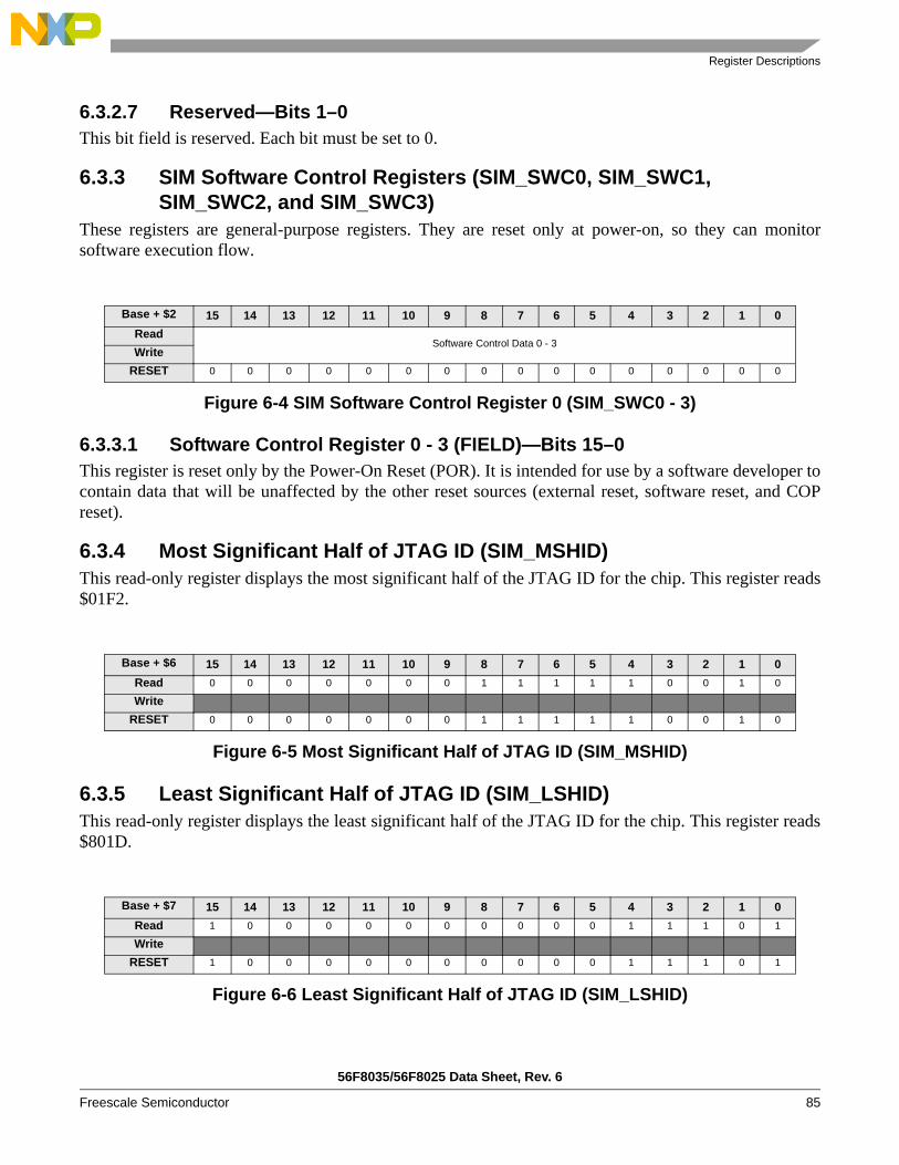
Register Descriptions
56F8035/56F8025 Data Sheet, Rev. 6
Freescale Semiconductor 85
6.3.2.7 Reserved—Bits 1–0This bit field is reserved. Each bit must be set to 0.
6.3.3 SIM Software Control Registers (SIM_SWC0, SIM_SWC1, SIM_SWC2, and SIM_SWC3)
These registers are general-purpose registers. They are reset only at power-on, so they can monitorsoftware execution flow.
Figure 6-4 SIM Software Control Register 0 (SIM_SWC0 - 3)
6.3.3.1 Software Control Register 0 - 3 (FIELD)—Bits 15–0This register is reset only by the Power-On Reset (POR). It is intended for use by a software developer tocontain data that will be unaffected by the other reset sources (external reset, software reset, and COPreset).
6.3.4 Most Significant Half of JTAG ID (SIM_MSHID)This read-only register displays the most significant half of the JTAG ID for the chip. This register reads$01F2.
Figure 6-5 Most Significant Half of JTAG ID (SIM_MSHID)
6.3.5 Least Significant Half of JTAG ID (SIM_LSHID)This read-only register displays the least significant half of the JTAG ID for the chip. This register reads$801D.
Figure 6-6 Least Significant Half of JTAG ID (SIM_LSHID)
Base + $2 15 14 13 12 11 10 9 8 7 6 5 4 3 2 1 0Read
Software Control Data 0 - 3Write
RESET 0 0 0 0 0 0 0 0 0 0 0 0 0 0 0 0
Base + $6 15 14 13 12 11 10 9 8 7 6 5 4 3 2 1 0Read 0 0 0 0 0 0 0 1 1 1 1 1 0 0 1 0
WriteRESET 0 0 0 0 0 0 0 1 1 1 1 1 0 0 1 0
Base + $7 15 14 13 12 11 10 9 8 7 6 5 4 3 2 1 0Read 1 0 0 0 0 0 0 0 0 0 0 1 1 1 0 1
WriteRESET 1 0 0 0 0 0 0 0 0 0 0 1 1 1 0 1

56F8035/56F8025 Data Sheet, Rev. 6
86 Freescale Semiconductor
6.3.6 SIM Power Control Register (SIM_PWR)This register controls the Standby mode of the large on-chip regulator. The large on-chip regulator derivesthe core digital logic power supply from the IO power supply. At a system bus frequency of 200kHz, thelarge regulator may be put in a reduced-power standby mode without interfering with device operation toreduce device power consumption. Refer to the overview of power-down modes and the overview of clockgeneration for more information on the use of large regulator standby.
Figure 6-7 SIM Power Control Register (SIM_PWR)
6.3.6.1 Reserved—Bits 15–2This bit field is reserved. Each bit must be set to 0.
6.3.6.2 Large Regulator Standby Mode (LRSTDBY)—Bits 1–0• 00 = Large regulator is in Normal mode• 01 = Large regulator is in Standby (reduced-power) mode• 10 = Large regulator is in Normal mode and the LRSTDBY field is write-protected until the next reset• 11 = Large regulator is in Standby mode and the LRSTDBY field is write-protected until the next reset
6.3.7 Clock Output Select Register (SIM_CLKOUT)The Clock Output Select register can be used to multiplex out selected clock sources generated inside theclock generation and SIM modules onto the muxed clock output pins. All functionality is for test purposesonly. Glitches may be produced when the clock is enabled or switched. The delay from the clock sourceto the output is unspecified. The observability of the clock output signals at output pads is subject to thefrequency limitations of the associated IO cell.
GPIOA[3:0] can function as GPIO, PWM, or as clock output pins. If GPIOA[3:0] are programmed tooperate as peripheral outputs, then the choice is between PWM and clock outputs. The default state is forthe peripheral function of GPIOA[3:0] to be programmed as PWM (selected by bits [9:6] of the ClockOutput Select register).
See Figure 6-8 for details.
Figure 6-8 CLKO Select Register (SIM_CLKOUT)
Base + $8 15 14 13 12 11 10 9 8 7 6 5 4 3 2 1 0Read 0 0 0 0 0 0 0 0 0 0 0 0 0 0
LRSTDBYWrite
RESET 0 0 0 0 0 0 0 0 0 0 0 0 0 0 0 0
Base + $A 15 14 13 12 11 10 9 8 7 6 5 4 3 2 1 0Read 0 0 0 0 0 0
PWM3 PWM2 PWM1 PWM01 0 0 0 0 0
WriteRESET 0 0 0 0 0 0 0 0 0 0 1 0 0 0 0 0
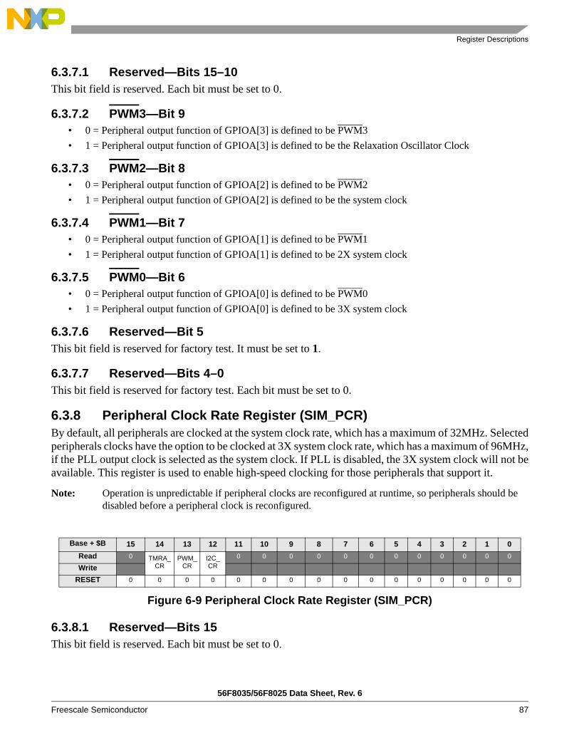
Register Descriptions
56F8035/56F8025 Data Sheet, Rev. 6
Freescale Semiconductor 87
6.3.7.1 Reserved—Bits 15–10This bit field is reserved. Each bit must be set to 0.
6.3.7.2 PWM3—Bit 9• 0 = Peripheral output function of GPIOA[3] is defined to be PWM3• 1 = Peripheral output function of GPIOA[3] is defined to be the Relaxation Oscillator Clock
6.3.7.3 PWM2—Bit 8• 0 = Peripheral output function of GPIOA[2] is defined to be PWM2• 1 = Peripheral output function of GPIOA[2] is defined to be the system clock
6.3.7.4 PWM1—Bit 7• 0 = Peripheral output function of GPIOA[1] is defined to be PWM1• 1 = Peripheral output function of GPIOA[1] is defined to be 2X system clock
6.3.7.5 PWM0—Bit 6• 0 = Peripheral output function of GPIOA[0] is defined to be PWM0• 1 = Peripheral output function of GPIOA[0] is defined to be 3X system clock
6.3.7.6 Reserved—Bit 5This bit field is reserved for factory test. It must be set to 1.
6.3.7.7 Reserved—Bits 4–0This bit field is reserved for factory test. Each bit must be set to 0.
6.3.8 Peripheral Clock Rate Register (SIM_PCR)By default, all peripherals are clocked at the system clock rate, which has a maximum of 32MHz. Selectedperipherals clocks have the option to be clocked at 3X system clock rate, which has a maximum of 96MHz,if the PLL output clock is selected as the system clock. If PLL is disabled, the 3X system clock will not beavailable. This register is used to enable high-speed clocking for those peripherals that support it.
Note: Operation is unpredictable if peripheral clocks are reconfigured at runtime, so peripherals should be disabled before a peripheral clock is reconfigured.
Figure 6-9 Peripheral Clock Rate Register (SIM_PCR)
6.3.8.1 Reserved—Bits 15This bit field is reserved. Each bit must be set to 0.
Base + $B 15 14 13 12 11 10 9 8 7 6 5 4 3 2 1 0Read 0 TMRA_
CRPWM_
CRI2C_CR
0 0 0 0 0 0 0 0 0 0 0 0
WriteRESET 0 0 0 0 0 0 0 0 0 0 0 0 0 0 0 0

56F8035/56F8025 Data Sheet, Rev. 6
88 Freescale Semiconductor
6.3.8.2 Quad Timer A Clock Rate (TMRA_CR)—Bit 14This bit selects the clock speed for the Quad Timer A module.
• 0 = Quad Timer A clock rate equals the system clock rate, to a maximum 32MHz (default)• 1 = Quad Timer A clock rate equals 3X system clock rate, to a maximum 96MHz
6.3.8.3 Pulse Width Modulator Clock Rate (PWM_CR)—Bit 13This bit selects the clock speed for the PWM module.
• 0 = PWM module clock rate equals the system clock rate, to a maximum 32MHz (default)• 1 = PWM module clock rate equals 3X system clock rate, to a maximum 96MHz
6.3.8.4 Inter-Integrated Circuit Run Clock Rate (I2C_CR)—Bit 12This bit selects the clock speed for the I2C run clock.
• 0 = I2C module run clock rate equals the system clock rate, to a maximum 32MHz (default)
• 1 = I2C module run clock rate equals 3X system clock rate, to a maximum 96MHz
6.3.8.5 Reserved—Bits 11–0This bit field is reserved. Each bit must be set to 0.
6.3.9 Peripheral Clock Enable Register 0 (SIM_PCE0)The Peripheral Clock Enable register enables or disables clocks to the peripherals as a power savingsfeature. Significant power savings are achieved by enabling only the peripheral clocks that are in use.When a peripheral’s clock is disabled, that peripheral is in Stop mode. Accesses made to a module that hasits clock disabled will have no effect. The corresponding peripheral should itself be disabled while its clockis shut off. IPBus writes are not possible.
Setting the PCE bit does not guarantee that the peripheral’s clock is running. Enabled peripheral clockswill still become disabled in Stop mode, unless the peripheral’s Stop Disable control in the SDn registeris set to 1.
Figure 6-10 Peripheral Clock Enable Register 0 (SIM_PCE0)
6.3.9.1 Comparator B Clock Enable (CMPB)—Bit 15• 0 = The clock is not provided to the Comparator B module (the Comparator B module is disabled)• 1 = The clock is enabled to the Comparator B module
6.3.9.2 Comparator A Clock Enable (CMPA)—Bit 14• 0 = The clock is not provided to the Comparator A module (the Comparator A module is disabled)• 1 = The clock is enabled to the Comparator A module
Base + $C 15 14 13 12 11 10 9 8 7 6 5 4 3 2 1 0
ReadCMPB CMPA DAC1 DAC0
0ADC
0 0 0I2C
0QSCI0
0QSPI0
0PWM
Write
RESET 0 0 0 0 0 0 0 0 0 0 0 0 0 0 0 0

Register Descriptions
56F8035/56F8025 Data Sheet, Rev. 6
Freescale Semiconductor 89
6.3.9.3 Digital-to-Analog Clock Enable 1 (DAC1)—Bit 13• 0 = The clock is not provided to the DAC1 module (the DAC1 module is disabled)• 1 = The clock is enabled to the DAC1 module
6.3.9.4 Digital-to-Analog Clock Enable 0 (DAC0)—Bit 12• 0 = The clock is not provided to the DAC0 module (the DAC0 module is disabled)• 1 = The clock is enabled to the DAC0 module
6.3.9.5 Reserved—Bit 11This bit field is reserved. It must be set to 0.
6.3.9.6 Analog-to-Digital Converter Clock Enable (ADC)—Bit 10• 0 = The clock is not provided to the ADC module (the ADC module is disabled)• 1 = The clock is enabled to the ADC module
6.3.9.7 Reserved—Bits 9–7This bit field is reserved. Each bit must be set to 0.
6.3.9.8 Inter-Integrated Circuit IPBus Clock Enable (I2C)—Bit 6• 0 = The clock is not provided to the I2C module (the I2C module is disabled)
• 1 = The clock is enabled to the I2C module
6.3.9.9 Reserved—Bit 5This bit field is reserved. It must be set to 0.
6.3.9.10 QSCI 0 Clock Enable (QSCI0)—Bit 4• 0 = The clock is not provided to the QSCI0 module (the QSCI0 module is disabled)• 1 = The clock is enabled to the QSCI0 module
6.3.9.11 Reserved—Bit 3This bit field is reserved. It must be set to 0.
6.3.9.12 QSPI 0 Clock Enable (QSPI0)—Bit 2• 0 = The clock is not provided to the QSPI0 module (the QSPI0 module is disabled)• 1 = The clock is enabled to the QSPI0 module
6.3.9.13 Reserved—Bit 1This bit field is reserved. It must be set to 0.
6.3.9.14 PWM Clock Enable (PWM)—Bit 0• 0 = The clock is not provided to the PWM module (the PWM module is disabled)
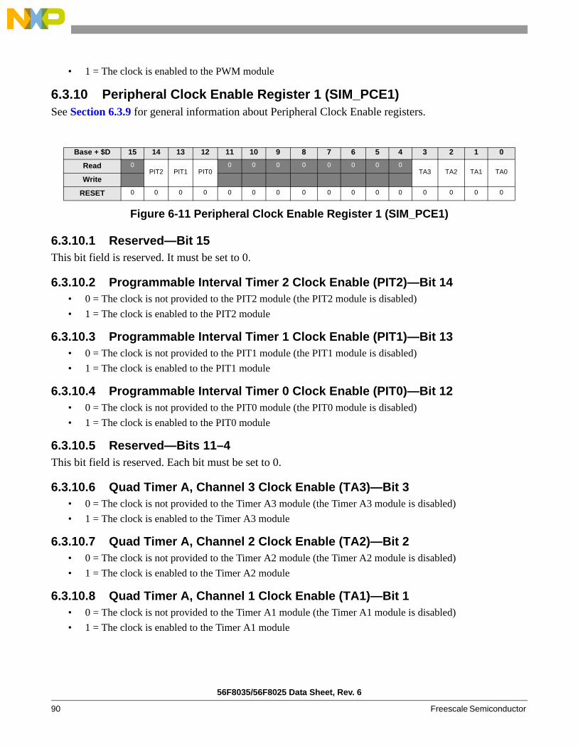
56F8035/56F8025 Data Sheet, Rev. 6
90 Freescale Semiconductor
• 1 = The clock is enabled to the PWM module
6.3.10 Peripheral Clock Enable Register 1 (SIM_PCE1)See Section 6.3.9 for general information about Peripheral Clock Enable registers.
Figure 6-11 Peripheral Clock Enable Register 1 (SIM_PCE1)
6.3.10.1 Reserved—Bit 15This bit field is reserved. It must be set to 0.
6.3.10.2 Programmable Interval Timer 2 Clock Enable (PIT2)—Bit 14• 0 = The clock is not provided to the PIT2 module (the PIT2 module is disabled)• 1 = The clock is enabled to the PIT2 module
6.3.10.3 Programmable Interval Timer 1 Clock Enable (PIT1)—Bit 13• 0 = The clock is not provided to the PIT1 module (the PIT1 module is disabled)• 1 = The clock is enabled to the PIT1 module
6.3.10.4 Programmable Interval Timer 0 Clock Enable (PIT0)—Bit 12• 0 = The clock is not provided to the PIT0 module (the PIT0 module is disabled)• 1 = The clock is enabled to the PIT0 module
6.3.10.5 Reserved—Bits 11–4This bit field is reserved. Each bit must be set to 0.
6.3.10.6 Quad Timer A, Channel 3 Clock Enable (TA3)—Bit 3• 0 = The clock is not provided to the Timer A3 module (the Timer A3 module is disabled)• 1 = The clock is enabled to the Timer A3 module
6.3.10.7 Quad Timer A, Channel 2 Clock Enable (TA2)—Bit 2• 0 = The clock is not provided to the Timer A2 module (the Timer A2 module is disabled)• 1 = The clock is enabled to the Timer A2 module
6.3.10.8 Quad Timer A, Channel 1 Clock Enable (TA1)—Bit 1• 0 = The clock is not provided to the Timer A1 module (the Timer A1 module is disabled)• 1 = The clock is enabled to the Timer A1 module
Base + $D 15 14 13 12 11 10 9 8 7 6 5 4 3 2 1 0
Read 0PIT2 PIT1 PIT0
0 0 0 0 0 0 0 0TA3 TA2 TA1 TA0
Write
RESET 0 0 0 0 0 0 0 0 0 0 0 0 0 0 0 0
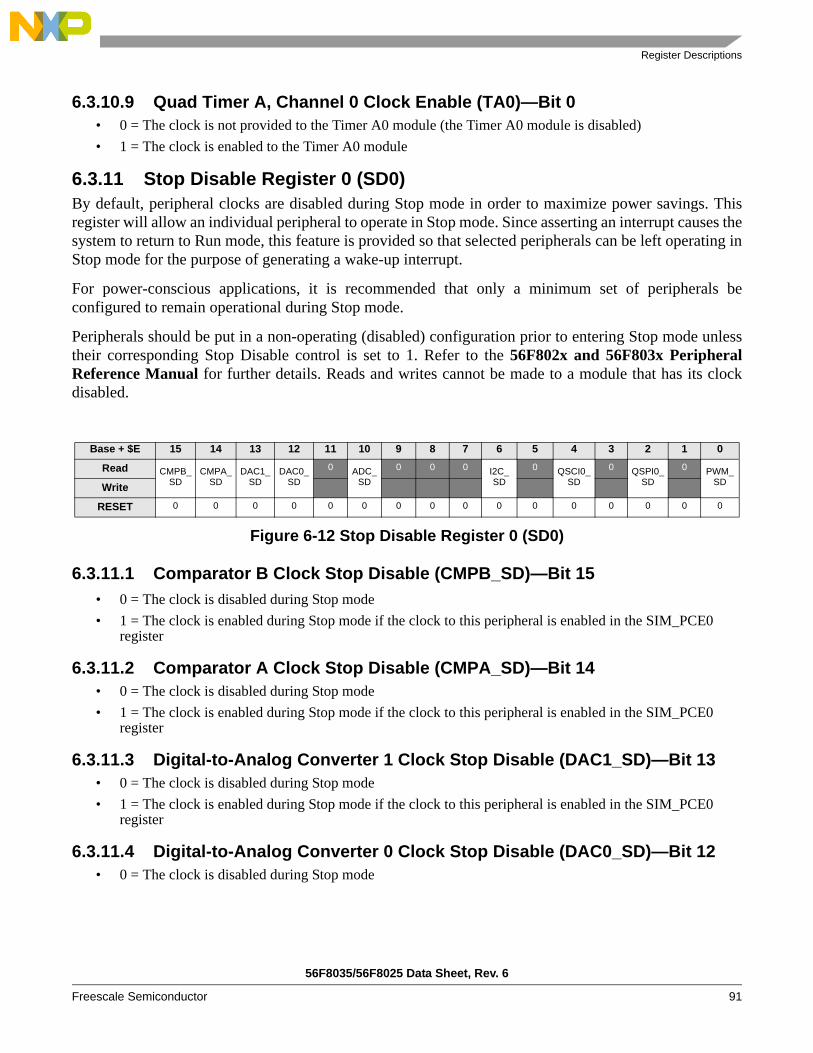
Register Descriptions
56F8035/56F8025 Data Sheet, Rev. 6
Freescale Semiconductor 91
6.3.10.9 Quad Timer A, Channel 0 Clock Enable (TA0)—Bit 0• 0 = The clock is not provided to the Timer A0 module (the Timer A0 module is disabled)• 1 = The clock is enabled to the Timer A0 module
6.3.11 Stop Disable Register 0 (SD0)By default, peripheral clocks are disabled during Stop mode in order to maximize power savings. Thisregister will allow an individual peripheral to operate in Stop mode. Since asserting an interrupt causes thesystem to return to Run mode, this feature is provided so that selected peripherals can be left operating inStop mode for the purpose of generating a wake-up interrupt.
For power-conscious applications, it is recommended that only a minimum set of peripherals beconfigured to remain operational during Stop mode.
Peripherals should be put in a non-operating (disabled) configuration prior to entering Stop mode unlesstheir corresponding Stop Disable control is set to 1. Refer to the 56F802x and 56F803x PeripheralReference Manual for further details. Reads and writes cannot be made to a module that has its clockdisabled.
Figure 6-12 Stop Disable Register 0 (SD0)
6.3.11.1 Comparator B Clock Stop Disable (CMPB_SD)—Bit 15• 0 = The clock is disabled during Stop mode• 1 = The clock is enabled during Stop mode if the clock to this peripheral is enabled in the SIM_PCE0
register
6.3.11.2 Comparator A Clock Stop Disable (CMPA_SD)—Bit 14• 0 = The clock is disabled during Stop mode• 1 = The clock is enabled during Stop mode if the clock to this peripheral is enabled in the SIM_PCE0
register
6.3.11.3 Digital-to-Analog Converter 1 Clock Stop Disable (DAC1_SD)—Bit 13• 0 = The clock is disabled during Stop mode• 1 = The clock is enabled during Stop mode if the clock to this peripheral is enabled in the SIM_PCE0
register
6.3.11.4 Digital-to-Analog Converter 0 Clock Stop Disable (DAC0_SD)—Bit 12• 0 = The clock is disabled during Stop mode
Base + $E 15 14 13 12 11 10 9 8 7 6 5 4 3 2 1 0
Read CMPB_ SD
CMPA_ SD
DAC1_SD
DAC0_SD
0 ADC_SD
0 0 0 I2C_SD
0 QSCI0_SD
0 QSPI0_SD
0 PWM_SDWrite
RESET 0 0 0 0 0 0 0 0 0 0 0 0 0 0 0 0

56F8035/56F8025 Data Sheet, Rev. 6
92 Freescale Semiconductor
• 1 = The clock is enabled during Stop mode if the clock to this peripheral is enabled in the SIM_PCE0 register
6.3.11.5 Reserved—Bit 11This bit field is reserved. It must be set to 0.
6.3.11.6 Analog-to-Digital Converter Clock Stop Disable (ADC_SD)—Bit 10• 0 = The clock is disabled during Stop mode• 1 = The clock is enabled during Stop mode if the clock to this peripheral is enabled in the SIM_PCE0
register
6.3.11.7 Reserved—Bits 9–7This bit field is reserved. Each bit must be set to 0.
6.3.11.8 Inter-Integrated Circuit Clock Stop Disable (I2C_SD)—Bit 6• 0 = The clock is disabled during Stop mode• 1 = The clock is enabled during Stop mode if the clock to this peripheral is enabled in the SIM_PCE0
register
6.3.11.9 Reserved—Bit 5This bit field is reserved. It must be set to 0.
6.3.11.10 QSCI0 Clock Stop Disable (QSCI0_SD)—Bit 4• 0 = The clock is disabled during Stop mode• 1 = The clock is enabled during Stop mode if the clock to this peripheral is enabled in the SIM_PCE0
register
6.3.11.11 Reserved—Bit 3This bit field is reserved. It must be set to 0.
6.3.11.12 QSPI0 Clock Stop Disable (QSPI0_SD)—Bit 2Each bit controls clocks to the indicated peripheral.
• 0 = The clock is disabled during Stop mode• 1 = The clock is enabled during Stop mode if the clock to this peripheral is enabled in the SIM_PCE0
register
6.3.11.13 Reserved—Bit 1This bit field is reserved. It must be set to 0.
6.3.11.14 PWM Clock Stop Disable (PWM_SD)—Bit 0• 0 = The clock is disabled during Stop mode• 1 = The clock is enabled during Stop mode if the clock to this peripheral is enabled in the SIM_PCE0
register
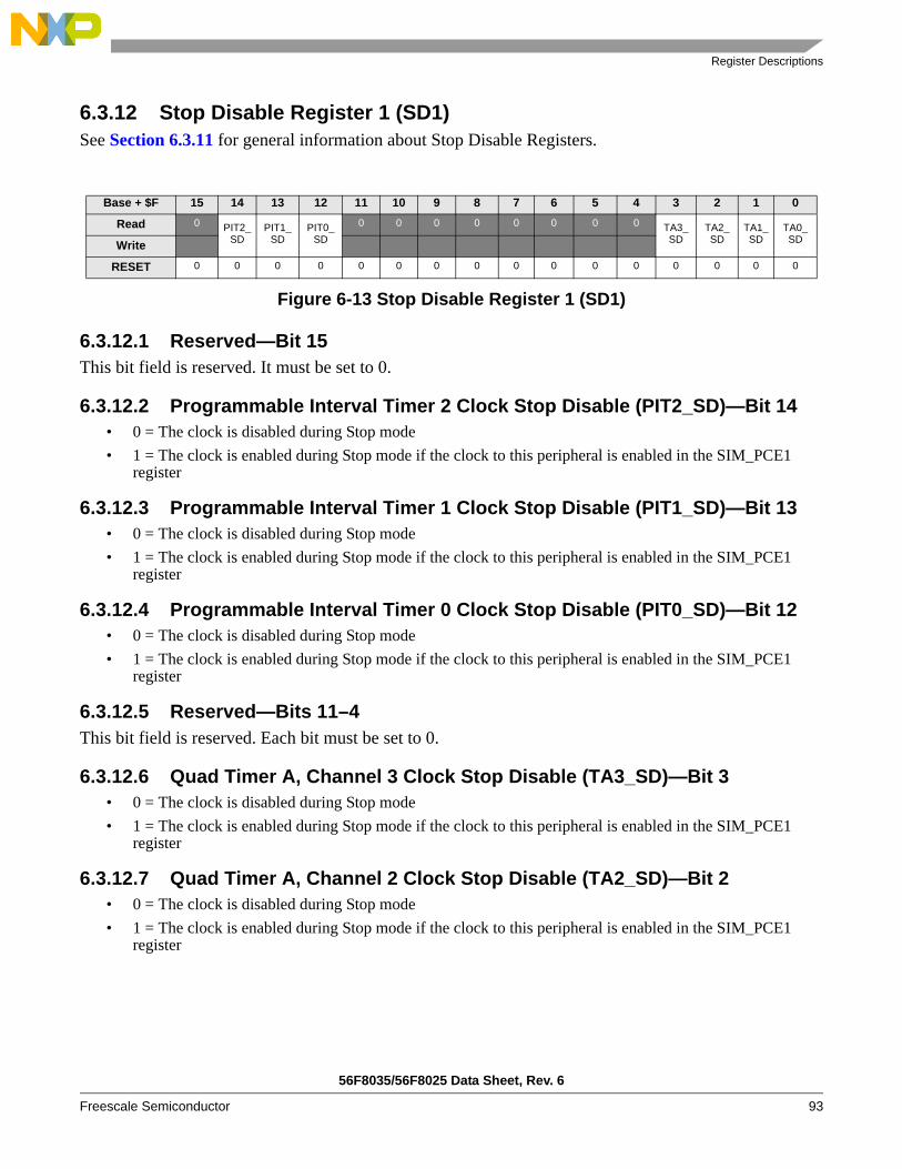
Register Descriptions
56F8035/56F8025 Data Sheet, Rev. 6
Freescale Semiconductor 93
6.3.12 Stop Disable Register 1 (SD1)See Section 6.3.11 for general information about Stop Disable Registers.
Figure 6-13 Stop Disable Register 1 (SD1)
6.3.12.1 Reserved—Bit 15This bit field is reserved. It must be set to 0.
6.3.12.2 Programmable Interval Timer 2 Clock Stop Disable (PIT2_SD)—Bit 14• 0 = The clock is disabled during Stop mode• 1 = The clock is enabled during Stop mode if the clock to this peripheral is enabled in the SIM_PCE1
register
6.3.12.3 Programmable Interval Timer 1 Clock Stop Disable (PIT1_SD)—Bit 13• 0 = The clock is disabled during Stop mode• 1 = The clock is enabled during Stop mode if the clock to this peripheral is enabled in the SIM_PCE1
register
6.3.12.4 Programmable Interval Timer 0 Clock Stop Disable (PIT0_SD)—Bit 12• 0 = The clock is disabled during Stop mode• 1 = The clock is enabled during Stop mode if the clock to this peripheral is enabled in the SIM_PCE1
register
6.3.12.5 Reserved—Bits 11–4This bit field is reserved. Each bit must be set to 0.
6.3.12.6 Quad Timer A, Channel 3 Clock Stop Disable (TA3_SD)—Bit 3• 0 = The clock is disabled during Stop mode• 1 = The clock is enabled during Stop mode if the clock to this peripheral is enabled in the SIM_PCE1
register
6.3.12.7 Quad Timer A, Channel 2 Clock Stop Disable (TA2_SD)—Bit 2• 0 = The clock is disabled during Stop mode• 1 = The clock is enabled during Stop mode if the clock to this peripheral is enabled in the SIM_PCE1
register
Base + $F 15 14 13 12 11 10 9 8 7 6 5 4 3 2 1 0
Read 0 PIT2_ SD
PIT1_SD
PIT0_SD
0 0 0 0 0 0 0 0 TA3_SD
TA2_SD
TA1_SD
TA0_SDWrite
RESET 0 0 0 0 0 0 0 0 0 0 0 0 0 0 0 0

56F8035/56F8025 Data Sheet, Rev. 6
94 Freescale Semiconductor
6.3.12.8 Quad Timer A, Channel 1 Clock Stop Disable (TA1_SD)—Bit 1• 0 = The clock is disabled during Stop mode• 1 = The clock is enabled during Stop mode if the clock to this peripheral is enabled in the SIM_PCE1
register
6.3.12.9 Quad Timer A, Channel 0 Clock Stop Disable (TA0_SD)—Bit 0• 0 = The clock is disabled during Stop mode• 1 = The clock is enabled during Stop mode if the clock to this peripheral is enabled in the SIM_PCE1
register
6.3.13 I/O Short Address Location Register High (SIM_IOSAHI)In I/O short address mode, the instruction specifies only 6 LSBs of the effective address; the upper 18 bitsare “hard coded” to a specific area of memory. This scheme allows efficient access to a 64-location areain peripheral space with single word instruction. Short address location registers specify the upper 18 bitsof I/O address, which are “hard coded”. These registers allow access to peripherals using I/O short addressmode, regardless of the physical location of the peripheral, as shown in Figure 6-14.
Figure 6-14 I/O Short Address Determination
With this register set, software can set the SIM_IOSAHI and SIM_IOSALO registers to point to itsperipheral registers and then use the I/O short addressing mode to access them.
Note: The default value of this register set points to the EOnCE registers.
Note: The pipeline delay between setting this register set and using short I/O addressing with the new value is five instruction cycles.
Instruction Portion“Hard Coded” Address Portion
6 Bits from I/O Short Address Mode Instruction
16 Bits from SIM_IOSALO Register
2 bits from SIM_IOSAHI Register
Full 24-Bit for Short I/O Address
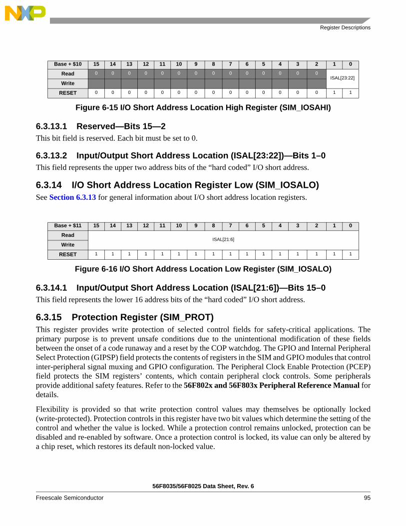
Register Descriptions
56F8035/56F8025 Data Sheet, Rev. 6
Freescale Semiconductor 95
Figure 6-15 I/O Short Address Location High Register (SIM_IOSAHI)
6.3.13.1 Reserved—Bits 15—2This bit field is reserved. Each bit must be set to 0.
6.3.13.2 Input/Output Short Address Location (ISAL[23:22])—Bits 1–0This field represents the upper two address bits of the “hard coded” I/O short address.
6.3.14 I/O Short Address Location Register Low (SIM_IOSALO)See Section 6.3.13 for general information about I/O short address location registers.
Figure 6-16 I/O Short Address Location Low Register (SIM_IOSALO)
6.3.14.1 Input/Output Short Address Location (ISAL[21:6])—Bits 15–0This field represents the lower 16 address bits of the “hard coded” I/O short address.
6.3.15 Protection Register (SIM_PROT)This register provides write protection of selected control fields for safety-critical applications. Theprimary purpose is to prevent unsafe conditions due to the unintentional modification of these fieldsbetween the onset of a code runaway and a reset by the COP watchdog. The GPIO and Internal PeripheralSelect Protection (GIPSP) field protects the contents of registers in the SIM and GPIO modules that controlinter-peripheral signal muxing and GPIO configuration. The Peripheral Clock Enable Protection (PCEP)field protects the SIM registers’ contents, which contain peripheral clock controls. Some peripheralsprovide additional safety features. Refer to the 56F802x and 56F803x Peripheral Reference Manual fordetails.
Flexibility is provided so that write protection control values may themselves be optionally locked(write-protected). Protection controls in this register have two bit values which determine the setting of thecontrol and whether the value is locked. While a protection control remains unlocked, protection can bedisabled and re-enabled by software. Once a protection control is locked, its value can only be altered bya chip reset, which restores its default non-locked value.
Base + $10 15 14 13 12 11 10 9 8 7 6 5 4 3 2 1 0
Read 0 0 0 0 0 0 0 0 0 0 0 0 0 0ISAL[23:22]
Write
RESET 0 0 0 0 0 0 0 0 0 0 0 0 0 0 1 1
Base + $11 15 14 13 12 11 10 9 8 7 6 5 4 3 2 1 0
ReadISAL[21:6]
Write
RESET 1 1 1 1 1 1 1 1 1 1 1 1 1 1 1 1

56F8035/56F8025 Data Sheet, Rev. 6
96 Freescale Semiconductor
Figure 6-17 Protection Register (SIM_PROT)
6.3.15.1 Reserved—Bits 15–4This bit field is reserved. Each bit must be set to 0.
6.3.15.2 Peripheral Clock Enable Protection (PCEP)—Bits 3–2These bits enable write protection of all fields in the PCEn, SDn, and PCR registers in the SIM module.
• 00 = Write protection off (default) • 01 = Write protection on• 10 = Write protection off and locked until chip reset• 11 = Write protection on and locked until chip reset
6.3.15.3 GPIO and Internal Peripheral Select Protection (GIPSP)—Bits 1–0These bits enable write protection of GPSn and IPSn registers in the SIM module and write protect allGPIOx_PEREN, GPIOx_PPOUTM and GPIOx_DRIVE registers in GPIO modules.
• 00 = Write protection off (default) • 01 = Write protection on• 10 = Write protection off and locked until chip reset• 11 = Write protection on and locked until chip reset
Note: The PWM fields in the CLKOUT register are also write protected by GIPSP. They are reserved for in-house test only.
6.3.16 SIM GPIO Peripheral Select Register 0 for GPIOA (SIM_GPSA0)Most I/O pins have an associated GPIO function. In addition to the GPIO function, I/O can be configuredto be one of several peripheral functions. The GPIOx_PEREN register within the GPIO module controlsthe selection between peripheral or GPIO control of the I/O pins. The GPIO function is selected when theGPIOx_PEREN bit for the I/O is 0. When the GPIOx_PEREN bit of the GPIO is 1, the fields in the GPSnregisters select which peripheral function has control of the I/O. Figure 6-18 illustrates the output path toan I/O pin when an I/O has two peripheral functions. Similar muxing is required on peripheral functioninputs to receive input from the properly selected I/O pin.
Base + $12 15 14 13 12 11 10 9 8 7 6 5 4 3 2 1 0Read 0 0 0 0 0 0 0 0 0 0 0 0
PCEP GIPSPWrite
RESET 0 0 0 0 0 0 0 0 0 0 0 0 0 0 0 0

Register Descriptions
56F8035/56F8025 Data Sheet, Rev. 6
Freescale Semiconductor 97
Figure 6-18 Overall Control of Signal Source Using SIM_GPSnn Control
In some cases, the user can choose peripheral function between several I/O, each of which have the optionto be programmed to control a specific peripheral function. If the user wishes to use that function, only oneof these I/O must be configured to control that peripheral function. If more than one I/O is configured tocontrol the peripheral function, the peripheral output signal will fan out to each I/O, but the peripheral inputsignal will be the logical OR and AND of all the I/O signals.
Complete lists of I/O muxings are provided in Table 2-3.
The GPSn setting can be altered during normal operation, but a delay must be inserted between the timewhen one function is disabled and another function is enabled.
Note: After reset, all I/O pins are GPIO, except the JTAG pins and the RESET pin.
Figure 6-19 GPIO Peripheral Select Register 0 for GPIOA (SIM_GPSA0)
6.3.16.1 Reserved—Bits 15–13This bit field is reserved. Each bit must be set to 0.
6.3.16.2 Configure GPIOA6 (GPS_A6)—Bit 12This field selects the alternate function for GPIOA6.
• 0 = FAULT0 - PWM FAULT0 Input (default)• 1 = TA0 - Timer A0
6.3.16.3 Configure GPIOA5 (GPS_A5)—Bits 11–10This field selects the alternate function for GPIOA5.
• 00 = PWM5 - PWM5 (default)
Base + $13 15 14 13 12 11 10 9 8 7 6 5 4 3 2 1 0Read 0 0 0
GPS_A6 GPS_A5 GPS_A40 0 0 0 0 0 0 0
WriteRESET 0 0 0 0 0 0 0 0 0 0 0 0 0 0 0 0
GPIOA6_PERENRegister
GPIOA6
GPIOA6 pin
SIM_GPSA0 Register
PWM FAULT0
Timer A0
0
1
0
1

56F8035/56F8025 Data Sheet, Rev. 6
98 Freescale Semiconductor
• 01 = FAULT2 - PWM FAULT2 Input• 10 = TA3 - Timer A3• 11 = Reserved
6.3.16.4 Configure GPIOA4 (GPS_A4)—Bits 9–8This field selects the alternate function for GPIOA4.
• 00 = PWM4 - PWM4 (default)• 01 = FAULT1 - PWM FAULT1 Input• 10 = TA2 - Timer A2• 11 = Reserved
6.3.16.5 Reserved—Bits 7–0This bit field is reserved. Each bit must be set to 0.
6.3.17 SIM GPIO Peripheral Select Register 1 for GPIOA (SIM_GPSA1)See Section 6.3.16 for general information about GPIO Peripheral Select Registers.
Figure 6-20 GPIO Peripheral Select Register 1 for GPIOA (SIM_GPSA1)
6.3.17.1 Reserved—Bits 15–7This bit field is reserved. Each bit must be set to 0.
6.3.17.2 Configure GPIOA11 (GPS_A11)—Bit 6This field selects the alternate function for GPIOA11.
• 0 = CINB - Comparator B Input 2 (default) • 1 = Reserved
6.3.17.3 Reserved—Bit 5This bit field is reserved. It must be set to 0.
6.3.17.4 Configure GPIOA10 (GPS_A10)—Bit 4This field selects the alternate function for GPIOA10.
• 0 = CINA- Comparator A Input 2 (default) • 1 = Reserved
6.3.17.5 Configure GPIOA9 (GPS_A9)—Bits 3–2This field selects the alternate function for GPIOA9.
Base + $14 15 14 13 12 11 10 9 8 7 6 5 4 3 2 1 0Read 0 0 0 0 0 0 0 0 0 GPS_
A110 GPS_
A10 GPS_A9 GPS_A8Write
RESET 0 0 0 0 0 0 0 0 0 0 0 0 0 0 0 0

Register Descriptions
56F8035/56F8025 Data Sheet, Rev. 6
Freescale Semiconductor 99
• 00 = FAULT2 - PWM FAULT2 Input (default) • 01 = TA3 - Timer A3• 10 = CMPBI1 - Comparator B Input 1• 11 = Reserved
6.3.17.6 Configure GPIOA8 (GPS_A8)—Bits 1–0This field selects the alternate function for GPIOA8.
• 00 = FAULT1 - PWM FAULT1 Input (default) • 01 = TA2 - Timer A2• 10 = CMPAI1 - Comparator A Input 1• 11 = Reserved
6.3.18 SIM GPIO Peripheral Select Register 0 for GPIOB (SIM_GPSB0)See Section 6.3.16 for general information about GPIO Peripheral Select Registers.
Figure 6-21 GPIO Peripheral Select Register 0 for GPIOB (SIM_GPSB0)
6.3.18.1 Reserved—Bit 15This bit field is reserved. It must be set to 0.
6.3.18.2 Configure GPIOB6 (GPS_B6)—Bits 14–13This field selects the alternate function for GPIOB6.
• 00 = RXD0 - QSCI0 Receive Data (default)
• 01 = SDA - I2C Serial Data• 10 = CLKIN - External Clock Input• 11 = Reserved
6.3.18.3 Configure GPIOB5 (GPS_B5)—Bits 12–11This field selects the alternate function for GPIOB5.
• 00 = TA1 - Timer A1 (default) • 01 = FAULT3 - PWM FAULT3 Input• 10 = CLKIN - External Clock Input• 11 = Reserved
6.3.18.4 Reserved—Bits 10–8This bit field is reserved. Each bit must be set to 0.
Base + $15 15 14 13 12 11 10 9 8 7 6 5 4 3 2 1 0Read 0
GPS_B6 GPS_B50 0 0
GPS_B3 GPS_B20 GPS_
B10 GPS_
B0WriteRESET 0 0 0 0 0 0 0 0 0 0 0 0 0 0 0 0

56F8035/56F8025 Data Sheet, Rev. 6
100 Freescale Semiconductor
6.3.18.5 Configure GPIOB3 (GPS_B3)—Bits 7–6This field selects the alternate function for GPIOB3.
• 00 = MOSI0 - QSPI0 Master Out/Slave In (default) • 01 = TA3 - Timer A3• 10 = PSRC1 - PWM2/PWM3 Pair External Source• 11 = Reserved
6.3.18.6 Configure GPIOB2 (GPS_B2)—Bits 5–4This field selects the alternate function for GPIOB2.
• 00 = MISO0 QSPI0 Master In/Slave Out (default) • 01 = TA2 - Timer A2• 10 = PSRC0 - PWM0/PWM1 Pair External Source• 11 = Reserved
6.3.18.7 Reserved—Bit 3This bit field is reserved. It must be set to 0.
6.3.18.8 Configure GPIOB1 (GPS_B1)—Bit 2This field selects the alternate function for GPIOB1.
• 0 = SS0 - QSPI0 Slave Select (default) • 1 = SDA - I2C Serial Data
6.3.18.9 Reserved—Bit 1This bit field is reserved. It must be set to 0.
6.3.18.10 Configure GPIOB0 (GPS_B0)—Bits 0This field selects the alternate function for GPIOB0.
• 0 = SCLK0 - QSPI0 Serial Clock (default)
• 1 = SCL - I2C Serial Clock
6.3.19 SIM GPIO Peripheral Select Register 1 for GPIOB (SIM_GPSB1)See Section 6.3.16 for general information about GPIO Peripheral Select Registers.
Figure 6-22 GPIO Peripheral Select Register 1 for GPIOB (SIM_GPSB1)
Base + $16 15 14 13 12 11 10 9 8 7 6 5 4 3 2 1 0Read 0 0 0 0 0 0 0 GPS_
B110 GPS_
B100 0 0 0 0 GPS_
B7WriteRESET 0 0 0 0 0 0 0 0 0 0 0 0 0 0 0 0
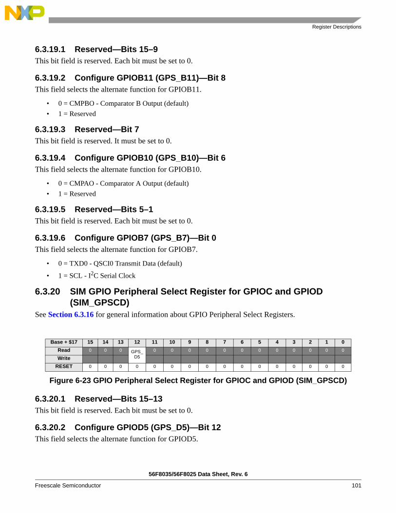
Register Descriptions
56F8035/56F8025 Data Sheet, Rev. 6
Freescale Semiconductor 101
6.3.19.1 Reserved—Bits 15–9This bit field is reserved. Each bit must be set to 0.
6.3.19.2 Configure GPIOB11 (GPS_B11)—Bit 8This field selects the alternate function for GPIOB11.
• 0 = CMPBO - Comparator B Output (default) • 1 = Reserved
6.3.19.3 Reserved—Bit 7This bit field is reserved. It must be set to 0.
6.3.19.4 Configure GPIOB10 (GPS_B10)—Bit 6This field selects the alternate function for GPIOB10.
• 0 = CMPAO - Comparator A Output (default) • 1 = Reserved
6.3.19.5 Reserved—Bits 5–1This bit field is reserved. Each bit must be set to 0.
6.3.19.6 Configure GPIOB7 (GPS_B7)—Bit 0This field selects the alternate function for GPIOB7.
• 0 = TXD0 - QSCI0 Transmit Data (default)
• 1 = SCL - I2C Serial Clock
6.3.20 SIM GPIO Peripheral Select Register for GPIOC and GPIOD (SIM_GPSCD)
See Section 6.3.16 for general information about GPIO Peripheral Select Registers.
Figure 6-23 GPIO Peripheral Select Register for GPIOC and GPIOD (SIM_GPSCD)
6.3.20.1 Reserved—Bits 15–13This bit field is reserved. Each bit must be set to 0.
6.3.20.2 Configure GPIOD5 (GPS_D5)—Bit 12This field selects the alternate function for GPIOD5.
Base + $17 15 14 13 12 11 10 9 8 7 6 5 4 3 2 1 0Read 0 0 0 GPS_
D50 0 0 0 0 0 0 0 0 0 0 0
WriteRESET 0 0 0 0 0 0 0 0 0 0 0 0 0 0 0 0
56F8035/56F8025 Data Sheet, Rev. 6
102 Freescale Semiconductor
• 0 = XTAL - External Crystal Oscillator Output (default) • 1 = CLKIN - External Clock Input
6.3.20.3 Reserved—Bits 11–0This bit field is reserved. Each bit must be set to 0.
6.3.21 Internal Peripheral Source Select Register 0 for Pulse Width Modulator (SIM_IPS0)
The internal integration of peripherals provides input signal source selection for peripherals where an inputsignal to a peripheral can be fed from one of several sources. These registers are organized by peripheraltype and provide a selection list for every peripheral input signal that has more than one alternative sourceto indicate which source is selected.
If one of the alternative sources is GPIO, the setting in these registers must be made consistently with thesettings in the GPSn and GPIOx_PEREN registers. Specifically, when an IPSn field is configured to selectan I/O pin as the source, then GPSn register settings must configure only one I/O pin to feed this peripheralinput function. Also, the GPIOx_PEREN bit for that I/O pin must be set to 1 to enable peripheral controlof the I/O.
Figure 6-24 Overall Control of Signal Source using SIM_IPSn Control
IPSn settings should not be altered while an affected peripheral is in an enabled (operational)configuration. See the 56F802x and 56F803x Peripheral Reference Manual for details.
GPIOA5_PERENRegister
GPIOA5
GPIOA5 pin
SIM_IPS0 Register
PWM FAULT2
Comparator A Output (Internal)
0
1
0
101
00
10
PWM5
Timer A3
SIM_GPSA0 Register

Register Descriptions
56F8035/56F8025 Data Sheet, Rev. 6
Freescale Semiconductor 103
Figure 6-25 Internal Peripheral Source Select Register for PWM (SIM_IPS0)
6.3.21.1 Reserved—Bits 15–14This bit field is reserved. Each bit must be set to 0.
6.3.21.2 Select Peripheral Input Source for FAULT2 (IPS0_FAULT2)—Bit 13This field selects the alternate input source signal to feed PWM input FAULT2.
• 0 = I/O Pin (External) - Use PWM FAULT2 Input Pin (default) • 1 = CMPBO (Internal) - Use Comparator B Output
6.3.21.3 Reserved—Bit 12This bit field is reserved. It must be set to 0.
6.3.21.4 Select Input Source for FAULT1 (IPS0_FAULT1)—Bit 11This field selects the alternate input source signal to feed PWM input FAULT1.
• 0 = I/O pin (External) - Use PWM FAULT2 Input Pin (default) • 1 = CMPAO (Internal) - Use Comparator A Output
6.3.21.5 Reserved—Bits 10–9This bit field is reserved. Each bit must be set to 0.
6.3.21.6 Select Peripheral Input Source for PWM4/PWM5 Pair Source (IPS0_PSRC2)—Bits 8–6
This field selects the alternate input source signal to feed PWM input PSRC2 as the PWM4/PWM5 pairsource.
• 000 = Reserved (default)• 001 = TA3 (Internal) - Use Timer A3 output as PWM source• 010 = ADC SAMPLE2 (Internal) - Use ADC SAMPLE2 result as PWM source
— If the ADC conversion result in SAMPLE2 is greater than the value programmed into the High Limit register HLMT2, then PWM4 is set to 0 and PWM5 is set to 1
— If the ADC conversion result in SAMPLE2 is less than the value programmed into the Low Limit register LLMT2, then PWM4 is set to 1 and PWM5 is set to 0
• 011 = CMPAO (Internal) - Use Comparator A output as PWM source• 100 = CMPBO (Internal) - Use Comparator B output as PWM source
Base + $18 15 14 13 12 11 10 9 8 7 6 5 4 3 2 1 0Read 0 0 IPS0_
FAULT20 IPS0_
FAULT10 0
IPS0_PSRC2 IPS0_PSRC1 IPS0_PSRC0Write
RESET 0 0 0 0 0 0 0 0 0 0 0 0 0 0 0 0

56F8035/56F8025 Data Sheet, Rev. 6
104 Freescale Semiconductor
• 11x = Reserved• 1x1 = Reserved
6.3.21.7 Select Peripheral Input Source for PWM2/PWM3 Pair Source (IPS0_PSRC1)—Bits 5–3
This field selects the alternate input source signal to feed PWM input PSRC1 as the PWM2/PWM3 pairsource.
• 000 = I/O pin (External) - Use a PSRC1 input pin as PWM source (default) • 001 = TA2 (Internal) - Use Timer A2 output as PWM source• 010 = ADC SAMPLE1 (Internal) - Use ADC SAMPLE1 result as PWM source
— If the ADC conversion result in SAMPLE1 is greater than the value programmed into the High Limit register HLMT1, then PWM2 is set to 0 and PWM3 is set to 1
— If the ADC conversion result in SAMPLE1 is less than the value programmed into the Low Limit register LLMT1, then PWM2 is set to 1 and PWM3 is set to 0
• 011 = CMPAO (Internal) - Use Comparator A output as PWM source• 100 = CMPBO (Internal) - Use Comparator B output as PWM source • 11x = Reserved• 1x1 = Reserved
6.3.21.8 Select Peripheral Input Source for PWM0/PWM1 Pair Source (IPS0_PSRC0)—Bits 2–0
This field selects the alternate input source signal to feed PWM input PSRC0 as the PWM0/PWM1 pairsource.
• 000 = I/O pin (External) - Use a PSRC0 input pin as PWM source (default) • 001 = TA0 (Internal) - Use Timer A0 output as PWM source• 010 = ADC SAMPLE0 (Internal) - Use ADC SAMPLE0 result as PWM source
— If the ADC conversion result in SAMPLE0 is greater than the value programmed into the High Limit register HLMT0, then PWM0 is set to 0 and PWM1 is set to 1
— If the ADC conversion result in SAMPLE0 is less than the value programmed into the Low Limit register LLMT0, then PWM0 is set to 1 and PWM1 is set to 0
• 011 = CMPAO (Internal) - Use Comparator A output as PWM source• 100 = CMPBO (Internal) - Use Comparator B output as PWM source • 11x = Reserved• 1x1 = Reserved
6.3.22 Internal Peripheral Source Select Register 1 for Digital-to-Analog Converters (SIM_IPS1)
See Section 6.3.21 for general information about Internal Peripheral Source Select registers.

Register Descriptions
56F8035/56F8025 Data Sheet, Rev. 6
Freescale Semiconductor 105
Figure 6-26 Internal Peripheral Source Select Register for DACs (SIM_IPS1)
6.3.22.1 Reserved—Bits 15–7This bit field is reserved. Each bit must be set to 0.
6.3.22.2 Select Input Source for SYNC Input to DAC 1 (IPS1_DSYNC1)—Bits 6–4This field selects the alternate input source signal to feed DAC1 SYNC input.
• 000 = PIT0 (Internal) - Use Programmable Interval Timer 0 Output as DAC SYNC input (default) • 001 = PIT1 (Internal) - Use Programmable Interval Timer 1 Output as DAC SYNC input• 010 = PIT2 (Internal) - Use Programmable Interval Timer 2 Output as DAC SYNC input• 011 = PWM SYNC (Internal) - Use PWM reload synchronization signal as DAC SYNC input• 100 = TA0 (Internal) - Use Timer A0 output as DAC SYNC input• 101 = TA1 (Internal) - Use Timer A1 output as DAC SYNC input• 11x = Reserved
6.3.22.3 Reserved—Bit 3This bit field is reserved. It must be set to 0.
6.3.22.4 Select Peripheral Input Source for SYNC Input to DAC 0 (IPS1_DSYNC0)—Bits 2–0
This field selects the alternate input source signal to feed DAC0 SYNC input.
• 000 = PIT0 (Internal) - Use Programmable Interval Timer 0 Output as DAC SYNC input (default) • 001 = PIT1 (Internal) - Use Programmable Interval Timer 1 Output as DAC SYNC input• 010 = PIT2 (Internal) - Use Programmable Interval Timer 2 Output as DAC SYNC input• 011 = PWM SYNC (Internal) - Use PWM reload synchronization signal as DAC SYNC input• 100 = TA0 (Internal) - Use Timer A0 output as DAC SYNC input• 101 = TA1 (Internal) - Use Timer A1 output as DAC SYNC input• 11x = Reserved
6.3.23 Internal Peripheral Source Select Register 2 for Quad Timer A (SIM_IPS2)
See Section 6.3.21 for general information about Internal Peripheral Source Select registers.
Base + $19 15 14 13 12 11 10 9 8 7 6 5 4 3 2 1 0Read 0 0 0 0 0 0 0 0 0
IPS1_DSYNC10
IPS1_DSYNC0Write
RESET 0 0 0 0 0 0 0 0 0 0 0 0 0 0 0 0

56F8035/56F8025 Data Sheet, Rev. 6
106 Freescale Semiconductor
Figure 6-27 Internal Peripheral Source Select Register for TMRA (SIM_IPS2)
6.3.23.1 Reserved—Bits 15–13This bit field is reserved. Each bit must be set to 0.
6.3.23.2 Select Input Source for TA3 (IPS2_TA3)—Bit 12This field selects the alternate input source signal to feed Quad Timer A, input 3.
• 0 = I/O pin (External) - Use Timer A3 input/output pin • 1 = PWM SYNC (Internal) - Use PWM reload synchronization signal
6.3.23.3 Reserved—Bits 11–9This bit field is reserved. Each bit must be set to 0.
6.3.23.4 Select Input Source for TA2 (IPS2_TA2)—Bit 8This field selects the alternate input source signal to feed Quad Timer A, input 2.
• 0 = I/O pin (External) - Use Timer A2 input/output pin • 1 = CMPBO (Internal) - Use Comparator B output
6.3.23.5 Reserved—Bits 7–5This bit field is reserved. Each bit must be set to 0.
6.3.23.6 Select Input Source for TA1 (IPS2_TA1)—Bit 4This field selects the alternate input source signal to feed Quad Timer A, input 1.
• 0 = I/O pin (External) - Use Timer A1 input/output pin • 1 = CMPAO (Internal) - Use Comparator A output
6.3.23.7 Reserved—Bits 3–0This bit field is reserved. Each bit must be set to 0.
For Timer A to detect the PWM SYNC signal, the clock rate of both the PWM module and Timer Amodule must be identical, at either the system clock rate or 3X system clock rate.
6.4 Clock Generation OverviewThe SIM uses the master clock (2X system clock) at a maximum of 64MHz from the OCCS module toproduce a system clock at a maximum of 32MHz for the peripheral, core, and memory. It divides the
Base + $1A 15 14 13 12 11 10 9 8 7 6 5 4 3 2 1 0Read 0 0 0 IPS2_
TA30 0 0 IPS2_
TA20 0 0 IPS2_
TA10 0 0 0
WriteRESET 0 0 0 0 0 0 0 0 0 0 0 0 0 0 0 0

Clock Generation Overview
56F8035/56F8025 Data Sheet, Rev. 6
Freescale Semiconductor 107
master clock by two and gates it with appropriate power mode and clock gating controls. A 3X systemhigh-speed peripheral clock input from OCCS operates at three times the system clock at a maximum of96MHz and can be an optional clock for PWM, Timer A, Timer B, and I2C modules. These clocks aregenerated by gating the 3X system high-speed peripheral clock with appropriate power mode and clockgating controls.
The OCCS configuration controls the operating frequency of the SIM’s master clocks. In the OCCS, eitheran external clock (CLKIN), a crystal oscillator, or the relaxation oscillator can be selected as the masterclock source (MSTR_OSC). An external clock can be operated at any frequency up to 64MHz. The crystaloscillator can be operated only at a maximum of 8MHz. The relaxation oscillator can be operated at fullspeed (8MHz), standby speed (200kHz using ROSB), or powered down (using ROPD). An 8MHzMSTR_OSC can be multiplied to 196MHz using the PLL and postscaled to provide a variety of high-speedclock rates. Either the postscaled PLL output or MSTR_OSC signal can be selected to produce the masterclocks to the SIM. When the PLL is selected, both the 3X system clock and the 2X system clock areenabled. If the PLL is not selected, the 3X system clock is disabled and the master clock is MSTR_OSC.
In combination with the OCCS module, the SIM provides power modes (see Section 6.5), clock enables,and clock rate controls to provide flexible control of clocking and power utilization. The clock ratecontrols enable the high-speed clocking option for the two quad timers (TMRA and TMRB) and PWM,but requires the PLL to be on and selected. Refer to the 56F802x and 56F803x Peripheral ReferenceManual for further details. The peripheral clock enable controls can be used to disable an individualperipheral clock when it is not used.

56F8035/56F8025 Data Sheet, Rev. 6
108 Freescale Semiconductor
6.5 Power-Saving ModesThe 56F8035/56F8025 operates in one of five Power-Saving modes, as shown in Table 6-2.
The power-saving modes provide additional power management options by disabling the clock,reconfiguring the voltage regulator clock generation to manage power utilization, as shown in Table 6-2.Run, Wait, and Stop modes provide methods of enabling/disabling the peripheral and/or core clocking asa group. Stop disable controls for an individual peripheral are provided in the SDn registers to override the
Table 6-2 Clock Operation in Power-Saving ModesMode Core Clocks Peripheral Clocks Description
Run Core and memory clocks enabled
Peripheral clocks enabled
Device is fully functional
Wait Core and memory clocks disabled
Peripheral clocks enabled
Core executes WAIT instruction to enter this mode. Typically used for power-conscious applications.Possible recoveries from Wait mode to Run mode are:1. Any interrupt2. Executing a Debug mode entry command during the 56800E core JTAG interface3. Any reset (POR, external, software, COP)
Stop Master clock generation in the OCCS remains operational, but the SIM disables the generation of system and peripheral clocks.
Core executes STOP instruction to enter this mode. Possible recoveries from Stop mode to Run mode are:1. Interrupt from any peripheral configured in the CTRL register to operate in Stop mode (TA0-3, QSCI0, PIT0-1, CAN, CMPA-B)2. Low-voltage interrupt3. Executing a Debug mode entry command using the 56800E core JTAG interface4. Any reset (POR, external, software, COP)
Standby The OCCS generates the master clock at a reduced frequency (400kHz). The PLL is disabled and the high-speed peripheral option is not available. System and peripheral clocks operate at 200kHz.
The user configures the OCCS and SIM to select the relaxation oscillator clock source (PRECS), shut down the PLL (PLLPD), put the relaxation oscillator in Standby mode (ROSB), and put the large regulator in Standby (LRSTDBY). The device is fully operational, but operating at a minimum frequency and power configuration. Recovery requires reversing the sequence used to enter this mode (allowing for PLL lock time).
Power-Down Master clock generation in the OCCS is completely shut down. All system and peripheral clocks are disabled.
The user configures the OCCS and SIM to enter Standby mode as shown in the previous description, followed by powering down the oscillator (ROPD). The only possible recoveries from this mode are:1. External Reset2. Power-On Reset

Resets
56F8035/56F8025 Data Sheet, Rev. 6
Freescale Semiconductor 109
default behavior of Stop mode. By asserting a peripheral’s Stop disable bit, the peripheral clock continuesto operate in Stop mode. This is useful to generate interrupts which will recover the device from Stop modeto Run mode. Standby mode provides normal operation but at very low speed and power utilization. It ispossible to invoke Stop or Wait mode while in Standby mode for even greater levels of power reduction.A 400kHz external clock can optionally be used in Standby mode to produce the required Standby 200kHzsystem clock rate. Power-down mode, which selects the ROSC clock source but shuts it off, fully disablesthe device and minimizes its power utilization but is only recoverable via reset.
When the PLL is not selected and the system bus is operating at 200kHz or less, the large regulator can beput into its Standby mode (LRSTDBY) to reduce the power utilization of that regulator.
All peripherals, except the COP/watchdog timer, run at the system clock frequency or optional 3X systemclock for PWM, Timers, and I2C. The COP timer runs at OSC_CLK / 1024. The maximum frequency ofoperation is 32MHz.
6.6 Resets The SIM supports five sources of reset, as shown in Figure 6-28. The two asynchronous sources are theexternal reset pin and the Power-On Reset (POR). The three synchronous sources are the software reset(SW reset), which is generated within the SIM itself by writing the SIM_CTRL register in Section 6.3.1,the COP time-out reset (COP_TOR), and the COP loss-of-reference reset (COP_LOR). The resetgeneration module has three reset detectors, which resolve into four primary resets. These are outlined inTable 6-3. The JTAG circuitry is reset by the Power-On Reset.
Figure 6-28 provides a graphic illustration of the details in Table 6-3. Note that the POR_Delay blocksuse the OSC_CLK as their time base, since other system clocks are inactive during this phase of reset.
Table 6-3 Primary System Resets
Reset Sources
Reset Signal POR External Software COP Comments
EXTENDED_POR X Stretched version of POR released 64 OSC_CLK cycles after POR deasserts
CLKGEN_RST X X X X Released 32 OSC_CLK cycles after all reset sources, including EXTENDED_POR, have released
PERIP_RST X X X X Releases 32 SYS_CLK cycles after the CLKGEN_RST is released
CORE_RST X X X X Releases 32 SYS_CLK cycles after PERIP_RST is released

56F8035/56F8025 Data Sheet, Rev. 6
110 Freescale Semiconductor
Figure 6-28 Sources of RESET Functional Diagram (Test modes not included)
POR resets are extended 64 OSC_CLK clocks to stabilize the power supply and clock source. All resetsare subsequently extended for an additional 32 OSC_CLK clocks and 64 system clocks as the variousinternal reset controls are released. Given the normal relaxation oscillator rate of 8MHz, the duration of aPOR reset from when power comes on to when code is running is 28µS. An external reset generationcircuit may also be used. A description of how these resets are used to initialize the clocking system andsystem modules is included in Section 6.7.
6.7 ClocksThe memory, peripheral and core clocks all operate at the same frequency (32MHz maximum), with theexception of the peripheral clocks for quad timers TMRA and TMRB and the PWM, which have the optionto operate at 3X system clock. The SIM is responsible for clock distributions.
While the SIM generates the ADC peripheral clock in the same way it generates all other peripheral clocks,the ADC standby and conversion clocks are generated by a direct interface between the ADC and theOCCS module.
EXTENDED_PORJTAG
MemorySubsystem
Peripherals
56800E
CORE_RST
Delay 32sys clocks
OCCSCLKGEN_RST
PERIP_RST
Delay 32sys clocks
pulse shaper
pulse shaper
SW Reset
pulse shaper
Delay 32OSC_CLK
Clock
pulse shaper
POR
Power-On Reset
(active low)
External RESET IN(active low)
RESET
Delay 64OSC_CLK
Clock
Delay blocks assert immediately and deassert only after the programmed number of clock cycles.
COMBINED_RST
COP_LOR(active low)
COP_TOR(active low)

Clocks
56F8035/56F8025 Data Sheet, Rev. 6
Freescale Semiconductor 111
The deassertion sequence of internal resets coordinates the device start up, including the clocking systemstart up. The sequence is described in the following steps:
1. As power is applied, the Relaxation Oscillator starts to operate. When a valid operating voltage is reached, the POR reset will release.
2. The release of POR reset permits operation of the POR reset extender. The POR extender generates an extended POR reset, which is released 64 OSC_CLK cycles after POR reset. This provides an additional time period for the clock source and power to stabilize.
3. A Combined reset consists of the OR of the extended POR reset, the external reset, the COP reset and Software reset. The entire device, except for the POR extender, is held reset as long as Combined reset is asserted. The release of Combined reset permits operation of the CTRL register, the Synchronous reset generator, and the CLKGEN reset extender.
4. The Synchronous reset generator generates a reset to the Software and COP reset logic. The COP and Software reset logic is released three OSC_CLK cycles after Combined reset deasserts. This provides a reasonable minimum duration to the reset for these specialized functions.
5. The CLKGEN reset extender generates the CLKGEN reset used by the clock generation logic. The CLKGEN reset is released 32 OSC_CLK cycles after Combined reset deasserts. This provides a window in which the SIM stabilizes the master clock inputs to the clock generator.
6. The release of CLKGEN reset permits operation of the clock generation logic and the Peripheral reset extender. The Peripheral reset extender generates the Peripheral reset, which is released 32 SYS_CLK cycles after CLKGEN reset. This provides a window in which peripheral and core logic remain clocked, but in reset, so that synchronous resets can be resolved.
7. The release of Peripheral reset permits operation of the peripheral logic and the Core reset extender. The Core reset extender generates the Core reset, which is released 32 SYS_CLK cycles after the Peripheral reset. This provides a window in which critical peripheral start-up functions, such as Flash Security in the Flash memory, can be implemented.
8. The release of Core reset permits execution of code by the 56800E core and marks the end of the system start-up sequence.
Figure 6-29 illustrates clock relationships to one another and to the various resets as the device comes outof reset. RST is assumed to be the logical AND of all active-low system resets (for example, POR, externalreset, COP and Software reset). In the 56F8035/56F8025, this signal will be stretched by the SIM for aperiod of time (up to 96 OSC_CLK clock cycles, depending upon the status of the POR) to create the clockgeneration reset signal (CLKGEN_RST). The SIM should deassert CLKGEN_RST synchronously withthe negative edge of OSC_CLK in order to avoid skew problems. CLKGEN_RST is delayed 32 SYS_CLKcycles to create the peripheral reset signal (PERIP_RST). PERIP_RST is then delayed by 32 SYS_CLKcycles to create CORE_RST. Both PERIP_RST and CORE_RST should be released on the negative edgeof SYS_CLK_D as shown. This phased releasing of system resets is necessary to give some peripherals(for example, the Flash interface unit) set-up time prior to the 56800E core becoming active.

56F8035/56F8025 Data Sheet, Rev. 6
112 Freescale Semiconductor
Figure 6-29 Timing Relationships of Reset Signal to Clocks
6.8 InterruptsThe SIM generates no interrupts.
Part 7 Security FeaturesThe 56F8025 offers security features intended to prevent unauthorized users from reading the contents ofthe flash memory (FM) array. The 56F8025’s flash security consists of several hardware interlocks thatprevent unauthorized users from gaining access to the flash array.
After flash security is set, an authorized user is still able to access on-chip memory if a user-definedsoftware subroutine, which reads and transfers the contents of internal memory via serial communicationperipherals, is included in the application software.
7.1 Operation with Security EnabledAfter the user has programmed flash with the application code, the 56F8025 can be secured byprogramming the security word $0002 into program memory location $00 7FF7. This non-volatile wordwill keep the device secured through reset and through power-down of the device. Refer to the flashmemory chapter in the 56F802x and 56F803x Peripheral Reference Manual for the details. When flash
RST
MSTR_OSC
CKGEN_RST
2X SYS_CLK
SYS_CLK
SYS_CLK_D
SYS_CLK_DIV2
PERIP_RST
CORE_RST
Switch on falling OSC_CLK96 MSTR_OSC cycles
Switch on falling SYS_CLK
32 SYS_CLK cycles delay
32 SYS_CLK cycles delay
Maximum Delay = 64 OSC_CLK cycles for POR reset extension and 32 OSC_CLK cycles for Combined reset extension
Switch on falling SYS_CLK

Flash Access Lock and Unlock Mechanisms
56F8035/56F8025 Data Sheet, Rev. 6
Freescale Semiconductor 113
security mode is enabled, the 56F8025 will disable the core EOnCE debug capabilities. Normal programexecution is otherwise unaffected.
7.2 Flash Access Lock and Unlock MechanismsThere are several methods that effectively lock or unlock the on-chip flash.
7.2.1 Disabling EOnCE AccessOn-chip flash can be read by issuing commands across the EOnCE port, which is the debug interface forthe 56800E CPU. The TCK, TMS, TDO, and TDI pins comprise a JTAG interface onto which the EOnCEport functionality is mapped. When the device boots, the chip-level JTAG TAP (Test Access Port) is activeand provides the chip’s boundary scan capability and access to the ID register, but proper implementationof flash security will block any attempt to access the internal flash memory via the EOnCE port whensecurity is enabled.
7.2.2 Flash Lockout Recovery Using JTAGIf the device is secured, one lockout recovery mechanism is the complete erasure of the internal flashcontents, including the configuration field, thus disabling security (the protection register is cleared). Thisdoes not compromise security, as the entire contents of the user’s secured code stored in flash are erasedbefore security is disabled on the device on the next reset or power-up sequence.
To start the lockout recovery sequence via JTAG, the JTAG public instruction(LOCKOUT_RECOVERY) must first be shifted into the chip-level TAP controller’s instruction register.Once the LOCKOUT_RECOVERY instruction has been shifted into the instruction register, the clockdivider value must be shifted into the corresponding 7-bit data register. After the data register has beenupdated, the user must transition the TAP controller into the RUN-TEST/IDLE state for the lockoutsequence to commence. The controller must remain in this state until the erase sequence is complete. Referto the 56F802x and 56F803x Peripheral Reference Manual for more details, or contact Freescale.
Note: Once the lockout recovery sequence has completed, the user must reset both the JTAG TAP controller and device to return to normal unsecured operation. Power-on reset will reset both too.
7.2.3 Flash Lockout Recovery using CodeWarriorCodeWarrior can unlock a device by selecting the Debug menu, then selecting DSP56800E, followed byUnlock Flash. Another mechanism is also built into CodeWarrior using the device’s memoryconfiguration file. The command “Unlock_Flash_on_Connect 1” in the .cfg file accomplishes the sametask as using the Debug menu.
This lockout recovery mechanism is the complete erasure of the internal flash contents, including theconfiguration field, thus disabling security (the protection register is cleared).
7.2.4 Flash Lockout Recovery without mass eraseA user can un-secure a secured device by programming the word $0000 into program memory location$00 7FF7. After completing the programming, both the JTAG TAP controller and the device must be reset

56F8035/56F8025 Data Sheet, Rev. 6
114 Freescale Semiconductor
in order to return to normal unsecured operation. Power-on reset will also reset both.
The user is responsible for directing the device to invoke the flash programming subroutine to reprogramthe word $0000 into program memory location $00 7FF7. This is done by, for example, toggling a specificpin or downloading a user-defined key through serial interfaces.
Note: Flash contents can only be programmed for 1s to 0s.
7.3 Product AnalysisThe recommended method of unsecuring a secured device for product analysis of field failures is via themethod described in section 7.2.4. The customer would need to supply Technical Support with the detailsof the protocol to access the subroutines in flash memory. An alternative method for performing analysison a secured device would be to mass-erase and reprogram the flash with the original code, but modify thesecurity word or not program the security word.
Part 8 General-Purpose Input/Output (GPIO)
8.1 IntroductionThis section is intended to supplement the GPIO information found in the 56F802x and 56F803xPeripheral Reference Manual and contains only chip-specific information. This information supersedesthe generic information in the 56F802x and 56F803x Peripheral Reference Manual.
8.2 ConfigurationThere are four GPIO ports defined on the 56F8035/56F8025. The width of each port, the associatedperipheral, and reset functions are shown in Table 8-1. The specific mapping of GPIO port pins is shownin Table 8-2. Additional details are shown in Tables 2-2 and 2-3.
Table 8-1 GPIO Ports Configuration
GPIO Port
Available Pins in
56F8035/56F8025
Peripheral Function Reset Function
A 12 PWM, Timer, QSPI, Comparator, Reset GPIO, RESET
B 9 QSPI, I2C, PWM, Clock, Comparator, Timer
GPIO
C 8 ADC, Comparator, QSCI GPIO
D 6 Clock, Oscillator, DAC, JTAG GPIO, JTAG

Configuration
56F8035/56F8025 Data Sheet, Rev. 6
Freescale Semiconductor 115
Table 8-2 GPIO External Signals Map
GPIO Function Peripheral Function LQFPPackage Pin Notes
GPIOA0 PWM0 40 Defaults to A0
GPIOA1 PWM1 39 Defaults to A1
GPIOA2 PWM2 32 Defaults to A2
GPIOA3 PWM3 33 Defaults to A3
GPIOA4 PWM4 / TA2 / FAULT1 31 SIM register SIM_GPS is used to select between PWM4, TA2, and FAULT1.Defaults to A4
GPIOA5 PWM5 / TA3 / FAULT2 27 SIM register SIM_GPS is used to select between PWM5, TA3, and FAULT2.Defaults to A5
GPIOA6 FAULT0 / TA0 24 SIM register SIM_GPS is used to select between FAULT0 and TA0.Defaults to A6
GPIOA7 RESET 21 Defaults to RESET
GPIOA8 FAULT1 / TA2 / CMPAI1 26 SIM register SIM_GPS is used to select between FAULT1, TA2, and CMPAI1.Defaults to A8
GPIOA9 FAULT2 / TA3 / CMPBI1 5 SIM register SIM_GPS is used to select between FAULT2, TA3, and CMPBI1.Defaults to A9
GPIOA10 CMPAI2 25 Defaults to A10
GPIOA11 CMPBI2 6 Defaults to A11
GPIOB0 SCLK0 / SCL 30 SIM register SIM_GPS is used to select between SCLK and SCL.Defaults to B0
GPIOB1 SS0 / SDA 2 SIM register SIM_GPS is used to select between SS0 and SDA.Defaults to B1
GPIOB2 MISO0 / TA2 / PSRC0 23 SIM register SIM_GPS is used to select between MISO0, TA2, and PSRC0.Defaults to B2

56F8035/56F8025 Data Sheet, Rev. 6
116 Freescale Semiconductor
GPIOB3 MOSI0 / TA3 / PSRC1 22 SIM register SIM_GPS is used to select between MOSI0, TA3 and PSRC1.Defaults to B3
GPIOB5 TA1 / FAULT3 / CLKIN 4 SIM register SIM_GPS is used to select between TA1, FAULT3, and CLKIN.CLKIN functionality is enabled using the PLL Control Register within the OCCS block.Defaults to B5
GPIOB6 RXD0 / SDA / CLKIN 1 SIM register SIM_GPS is used to select between RXD0, SDA, and CLKIN. CLKIN functionality is enabled using the PLL Control Register within the OCCS block.Defaults to B6
GPIOB7 TXD0 / SCL 3 SIM register SIM_GPS is used to select between TXD0 and SCL.Defaults to B7
GPIOB10 CMPAO 20 Defaults to B10
GPIOB11 CMPBO 42 Defaults to B11
GPIOC0 ANA0 / CMPAI3 16 SIM register SIM_GPS is used to select between ANA0 and CMPAI3.Defaults to C0
GPIOC1 ANA1 15 Defaults to C1
GPIOC2 ANA2 / VREFHA 14 SIM register SIM_GPS is used to select between ANA2 and VREFHA.Defaults to C2
GPIOC3 ANA3 / VREFLA 13 SIM register SIM_GPS is used to select between ANA3 and VREFLA.Defaults to C3
GPIOC4 ANB0 / CMPBI3 7 SIM register SIM_GPS is used to select between ANB0 and CMPBI3.Defaults to C4
GPIOC5 ANB1 8 Defaults to C5
GPIOC6 ANB2 / VREFHB 9 SIM register SIM_GPS is used to select between ANB2 and VREFHB.Defaults to C6
GPIOC7 ANB3 / VREFLB 10 SIM register SIM_GPS is used to select between ANB3 and VREFLB.Defaults to C7
Table 8-2 GPIO External Signals Map (Continued)
GPIO Function Peripheral Function LQFPPackage Pin Notes

Reset Values
56F8035/56F8025 Data Sheet, Rev. 6
Freescale Semiconductor 117
8.3 Reset ValuesTables 8-1 and 8-2 detail registers for the 56F8035/56F8025; Figures 8-1 through 8-4 summarize registermaps and reset values.
GPIOD0 TDI 41 Defaults to TDI
GPIOD1 TDO 44 Defaults to TDO
GPIOD2 TCK 19 Defaults to TCK
GPIOD3 TMS 43 Defaults to TMS
GPIOD4 EXTAL 38 Defaults to D4
GPIOD5 XTAL / CLKIN 37 SIM register SIM_GPSCD is used to select between XTAL and CLKIN.Defaults to D5
Table 8-2 GPIO External Signals Map (Continued)
GPIO Function Peripheral Function LQFPPackage Pin Notes

56F8035/56F8025 Data Sheet, Rev. 6
118 Freescale Semiconductor
Figure 8-1 GPIOA Register Map Summary
Add. Offset Register Acronym 15 14 13 12 11 10 9 8 7 6 5 4 3 2 1 0
$0 GPIOA_PUPENR 0 0 0 0
PU[15:0]WRS 0 1 1 1 1 1 1 1 1 1 1 1 1 1 1 1
$1 GPIOA_DATAR .0 .0 .0 .0
D[15:0]WRS 0 0 0 0 0 0 0 0 0 0 0 0 0 0 0 0
$2 GPIOA_DDIRR .0. .0. .0. .0.
DD[15:0]WRS 0 0 0 0 0 0 0 0 0 0 0 0 0 0 0 0
$3 GPIOA_PERENR 0 0 0 0
PE[15:0]WRS 0 0 0 0 0 0 0 0 0 0 0 0 0 0 0 0
$4 GPIOA_IASSRTR 0 0 0 0
IA[15:0]WRS 0 0 0 0 0 0 0 0 0 0 0 0 0 0 0 0
$5 GPIOA_IENR 0 0 0 0
IEN[15:0]WRS 0 0 0 0 0 0 0 0 0 0 0 0 0 0 0 0
$6 GPIOA_IEPOLR 0 0 0 0
IEPOL[15:0]WRS 0 0 0 0 0 0 0 0 0 0 0 0 0 0 0 0
$7 GPIOA_IPENDR 0 0 0 0 IPR[15:0]WRS 0 0 0 0 0 0 0 0 0 0 0 0 0 0 0 0
$8 GPIOA_IEDGER 0 0 0 0
IES[15:0]WRS 0 0 0 0 0 0 0 0 0 0 0 0 0 0 0 0
$9 GPIOA_PPOUTMR 0 0 0 0
OEN[15:0]WRS 0 1 1 1 1 1 1 1 1 1 1 1 1 1 1 1
$A GPIOA_RDATAR 0 0 0 0 RAW DATA[15:0]WRS 0 X X X X X X X X X X X X X X X
$B GPIOA_DRIVER 0 0 0 0
DRIVE[15:0]WRS 0 0 0 0 0 0 0 0 0 0 0 0 0 0 0 0
R 0 Read as 0W ReservedRS Reset

Reset Values
56F8035/56F8025 Data Sheet, Rev. 6
Freescale Semiconductor 119
Figure 8-2 GPIOB Register Map Summary
Add. Offset Register Acronym 15 14 13 12 11 10 9 8 7 6 5 4 3 2 1 0
$0 GPIOB_PUPENR 0 0 0 0
PU[15:0]0 0
PU0
PUWRS 0 0 1 1 1 1 1 1 1 1 1 1 1 1 1 1
$1 GPIOB_DATAR 0 0 0 0
D[15:0]0 0
D0
DWRS 0 0 0 0 0 0 0 0 0 0 0 0 0 0 0 0
$2 GPIOB_DDIRR 0 0 0 0 DD[15:0] 0 0 DD 0 DDW
RS 0 0 0 0 0 0 0 0 0 0 0 0 0 0 0 0
$3 GPIOB_PERENR 0 0 0 0
PE[15:0]0 0
PE0
PEWRS 0 0 0 0 0 0 0 0 0 0 0 0 0 0 0 0
$4 GPIOB_IASSRTR 0 0 0 0
IA[15:0]0 0
IA0
IAWRS 0 0 0 0 0 0 0 0 0 0 0 0 0 0 0 0
$5 GPIOB_IENR 0 0 0 0
IEN[15:0]0 0
IEN0 IENW
RS 0 0 0 0 0 0 0 0 0 0 0 0 0 0 0 0
$6 GPIOB_IEPOLR 0 0 0 0
IEPOL[15:0]0 0
IEPOL0
IEPOLWRS 0 0 0 0 0 0 0 0 0 0 0 0 0 0 0 0
$7 GPIOB_IPENDR 0 0 0 0 IPR[15:0] 0 0 IPR 0 IPRWRS 0 0 0 0 0 0 0 0 0 0 0 0 0 0 0 0
$8 GPIOB_IEDGER 0 0 0 0
IES[15:0]0 0
IES0
IESWRS 0 0 0 0 0 0 0 0 0 0 0 0 0 0 0 0
$9 GPIOB_PPOUTMR 0 0 0 0
OEN[15:0]0 0
OEN0
OENWRS 0 0 1 1 1 1 1 1 1 1 1 1 1 1 1 1
$A GPIOB_RDATAR 0 0 0 0
RAW DATA[15:0]
0 0 RAW DATA 0 RAW DATA
WRS 0 0 X X X X X X X X X X X X X X
$B GPIOB_DRIVER 0 0 0 0
DRIVE[15:0]0 0
DRIVE0
DRIVEWRS 0 0 0 0 0 0 0 0 0 0 0 0 0 0 0 0
R 0 Read as 0W ReservedRS Reset

56F8035/56F8025 Data Sheet, Rev. 6
120 Freescale Semiconductor
Figure 8-3 GPIOC Register Map Summary
Add. Offset Register Acronym 15 14 13 12 11 10 9 8 7 6 5 4 3 2 1 0
$0 GPIOC_PUPENR 0 0 0 0 0 0 0 0
PU[15:0]WRS 1 1 1 1 1 1 1 1 1 1 1 1 1 1 1 1
$1 GPIOC_DATAR 0 0 0 0 0 0 0 0
D[15:0]WRS 0 0 0 0 0 0 0 0 0 0 0 0 0 0 0 0
$2 GPIOC_DDIRR 0 0 0 0 0 0 0 0
DD[15:0]WRS 0 0 0 0 0 0 0 0 0 0 0 0 0 0 0 0
$3 GPIOC_PERENR 0 0 0 0 0 0 0 0
PE[15:0]WRS 0 0 0 0 0 0 0 0 0 0 0 0 0 0 0 0
$4 GPIOC_IASSRTR 0 0 0 0 0 0 0 0
IA[15:0]WRS 0 0 0 0 0 0 0 0 0 0 0 0 0 0 0 0
$5 GPIOC_IENR 0 0 0 0 0 0 0 0
IEN[15:0]WRS 0 0 0 0 0 0 0 0 0 0 0 0 0 0 0 0
$6 GPIOC_IEPOLR 0 0 0 0 0 0 0 0
IEPOL[15:0]WRS 0 0 0 0 0 0 0 0 0 0 0 0 0 0 0 0
$7 GPIOC_IPENDR 0 0 0 0 0 0 0 0 IPR[15:0]WRS 0 0 0 0 0 0 0 0 0 0 0 0 0 0 0 0
$8 GPIOC_IEDGER 0 0 0 0 0 0 0 0
IES[15:0]WRS 0 0 0 0 0 0 0 0 0 0 0 0 0 0 0 0
$9 GPIOC_PPOUTMR 0 0 0 0 0 0 0 0
OEN[15:0]WRS 1 1 1 1 1 1 1 1 1 1 1 1 1 1 1 1
$A GPIOC_RDATAR 0 0 0 0 0 0 0 0 RAW DATA[15:0]WRS X X X X X X X X X X X X X X X X
$B GPIOC_DRIVER 0 0 0 0 0 0 0 0
DRIVE[15:0]WRS 0 0 0 0 0 0 0 0 0 0 0 0 0 0 0 0
R 0 Read as 0W ReservedRS Reset

Reset Values
56F8035/56F8025 Data Sheet, Rev. 6
Freescale Semiconductor 121
Figure 8-4 GPIOD Register Map Summary
Add. Offset Register Acronym 15 14 13 12 11 10 9 8 7 6 5 4 3 2 1 0
$0 GPIOD_PUPENR
PU[15:0]WRS 0 0 0 0 0 0 0 0 1 1 1 1 1 1 1 1
$1 GPIOD_DATAR
D[15:0]WRS 0 0 0 0 0 0 0 0 0 0 0 0 0 0 0 0
$2 GPIOD_DDIRR
DD[15:0]WRS 0 0 0 0 0 0 0 0 0 0 0 0 0 0 0 0
$3 GPIOD_PERENR
PE[15:0]WRS 0 0 0 0 0 0 0 0 0 0 0 0 1 1 1 1
$4 GPIOD_IASSRTR
IA[15:0]WRS 0 0 0 0 0 0 0 0 0 0 0 0 0 0 0 0
$5 GPIOD_IENR
IEN[15:0]WRS 0 0 0 0 0 0 0 0 0 0 0 0 0 0 0 0
$6 GPIOD_IEPOLR
IEPOL[15:0]WRS 0 0 0 0 0 0 0 0 0 0 0 0 0 0 0 0
$7 GPIOD_IPENDR IPR[15:0]WRS 0 0 0 0 0 0 0 0 0 0 0 0 0 0 0 0
$8 GPIOD_IEDGER
IES[15:0]WRS 0 0 0 0 0 0 0 0 0 0 0 0 0 0 0 0
$9 GPIOD_PPOUTMR
OEN[15:0]WRS 0 0 0 0 0 0 0 0 1 1 1 1 1 1 1 1
$A GPIOD_RDATAR RAW DATA[15:0]WRS 0 0 0 0 0 0 0 0 X X X X X X X X
$B GPIOD_DRIVER
DRIVE[15:0]WRS 0 0 0 0 0 0 0 0 0 0 0 0 0 0 0 0
R 0 Read as 0W ReservedRS Reset

56F8035/56F8025 Data Sheet, Rev. 6
122 Freescale Semiconductor
Part 9 Joint Test Action Group (JTAG)
9.1 56F8035/56F8025 InformationPlease contact your Freescale sales representative or authorized distributor for device/package-specificBSDL information.
The TRST pin is not available in this package. The pin is tied to VDD in the package.
The JTAG state machine is reset during POR and can also be reset via a soft reset by holding TMS highfor five rising edges of TCK, as described in the 56F802x and 56F803x Peripheral Reference Manual.
Part 10 Specifications
10.1 General CharacteristicsThe 56F8035/56F8025 is fabricated in high-density CMOS with 5V-tolerant TTL-compatible digitalinputs. The term “5V-tolerant” refers to the capability of an I/O pin, built on a 3.3V-compatible processtechnology, to withstand a voltage up to 5.5V without damaging the device. Many systems have a mixtureof devices designed for 3.3V and 5V power supplies. In such systems, a bus may carry both 3.3V- and5V-compatible I/O voltage levels (a standard 3.3V I/O is designed to receive a maximum voltage of 3.3V± 10% during normal operation without causing damage). This 5V-tolerant capability therefore offers thepower savings of 3.3V I/O levels, combined with the ability to receive 5V levels without damage.
Absolute maximum ratings in Table 10-1 are stress ratings only, and functional operation at the maximumis not guaranteed. Stress beyond these ratings may affect device reliability or cause permanent damage tothe device.
Unless otherwise stated, all specifications within this chapter apply over the temperature range of -40ºC to 125ºC ambient temperature over the following supply ranges: VSS = VSSA = 0V, VDD = VDDA = 3.0–3.6V, CL < 50pF, fOP = 32MHz
CAUTION
This device contains protective circuitry to guardagainst damage due to high static voltage or electricalfields. However, normal precautions are advised toavoid application of any voltages higher thanmaximum-rated voltages to this high-impedance circuit.Reliability of operation is enhanced if unused inputs aretied to an appropriate voltage level.
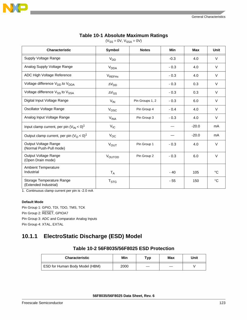
General Characteristics
56F8035/56F8025 Data Sheet, Rev. 6
Freescale Semiconductor 123
Default ModePin Group 1: GPIO, TDI, TDO, TMS, TCKPin Group 2: RESET, GPIOA7Pin Group 3: ADC and Comparator Analog InputsPin Group 4: XTAL, EXTAL
10.1.1 ElectroStatic Discharge (ESD) Model
Table 10-1 Absolute Maximum Ratings (VSS = 0V, VSSA = 0V)
Characteristic Symbol Notes Min Max Unit
Supply Voltage Range VDD -0.3 4.0 V
Analog Supply Voltage Range VDDA - 0.3 4.0 V
ADC High Voltage Reference VREFHx - 0.3 4.0 V
Voltage difference VDD to VDDA ΔVDD - 0.3 0.3 V
Voltage difference VSS to VSSA ΔVSS - 0.3 0.3 V
Digital Input Voltage Range VIN Pin Groups 1, 2 - 0.3 6.0 V
Oscillator Voltage Range VOSC Pin Group 4 - 0.4 4.0 V
Analog Input Voltage Range VINA Pin Group 3 - 0.3 4.0 V
Input clamp current, per pin (VIN < 0)1
1. Continuous clamp current per pin is -2.0 mA
VIC — -20.0 mA
Output clamp current, per pin (VO < 0)1 VOC — -20.0 mA
Output Voltage Range (Normal Push-Pull mode)
VOUT Pin Group 1 - 0.3 4.0 V
Output Voltage Range (Open Drain mode)
VOUTOD Pin Group 2 - 0.3 6.0 V
Ambient TemperatureIndustrial TA - 40 105 °C
Storage Temperature Range (Extended Industrial)
TSTG - 55 150 °C
Table 10-2 56F8035/56F8025 ESD Protection
Characteristic Min Typ Max Unit
ESD for Human Body Model (HBM) 2000 — — V

56F8035/56F8025 Data Sheet, Rev. 6
124 Freescale Semiconductor
1. Theta-JA determined on 2s2p test boards is frequently lower than would be observed in an application. Determined on 2s2p thermal test board.
2. Junction to ambient thermal resistance, Theta-JA (RθJA), was simulated to be equivalent to the JEDEC specification JESD51-2in a horizontal configuration in natural convection. Theta-JA was also simulated on a thermal test board with two internal planes(2s2p, where “s” is the number of signal layers and “p” is the number of planes) per JESD51-6 and JESD51-7. The correct namefor Theta-JA for forced convection or with the non-single layer boards is Theta-JMA.
3. Junction to case thermal resistance, Theta-JC (RθJC), was simulated to be equivalent to the measured values using the cold platetechnique with the cold plate temperature used as the “case” temperature. The basic cold plate measurement technique is de-scribed by MIL-STD 883D, Method 1012.1. This is the correct thermal metric to use to calculate thermal performance when thepackage is being used with a heat sink.
4. Junction to board thermal resistance, Theta-JB (RθJB), is a metric of the thermal resistance from the junction to the printed circuitboard determined per JESD51-8. Board temperature is measured on the top surface of the board near the package.
5. Thermal Characterization Parameter, Psi-JT (YJT), is the “resistance” from junction to reference point thermocouple on top centerof case as defined in JESD51-2. YJT is a useful value to use to estimate junction temperature in steady state customer environments.
6. Junction temperature is a function of die size, on-chip power dissipation, package thermal resistance, mounting site (board) temperature, ambient temperature, air flow, power dissipation of other components on the board, and board thermal resistance.
7. See Section 12.1 for more details on thermal design considerations.
ESD for Machine Model (MM) 200 — — V
ESD for Charge Device Model (CDM) 750 — — V
Table 10-3 LQFP Package Thermal Characteristics6
Characteristic Comments Symbol Value(LQFP) Unit Notes
Junction to ambientNatural convection
Single layer board (1s)
RθJA 41 °C/W 2
Junction to ambientNatural convection
Four layer board (2s2p)
RθJMA 34 °C/W 1, 2
Junction to ambient (@200 ft/min)
Single layer board (1s)
RθJMA 34 °C/W 2
Junction to ambient (@200 ft/min)
Four layer board (2s2p)
RθJMA 29 °C/W 1, 2
Junction to board RθJB 24 °C/W 4
Junction to case RθJC 8 °C/W 3
Junction to package top Natural Convection ΨJT 2 °C/W 5
Table 10-2 56F8035/56F8025 ESD Protection
Characteristic Min Typ Max Unit
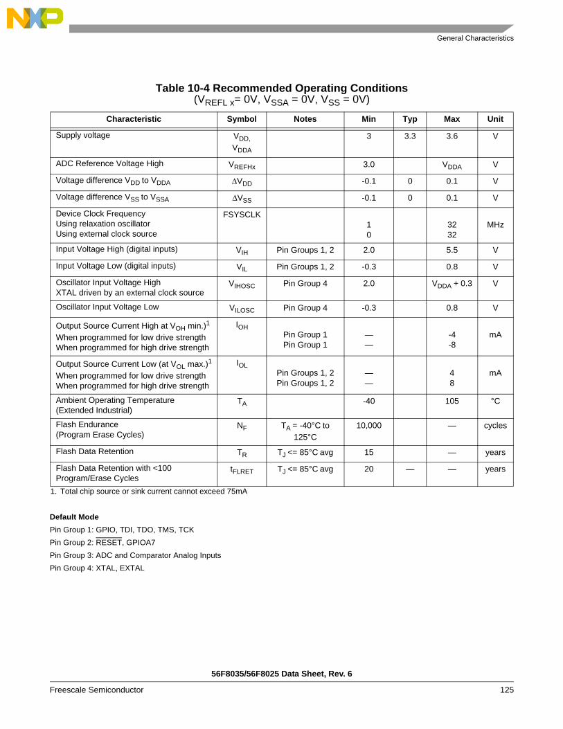
General Characteristics
56F8035/56F8025 Data Sheet, Rev. 6
Freescale Semiconductor 125
Default ModePin Group 1: GPIO, TDI, TDO, TMS, TCKPin Group 2: RESET, GPIOA7Pin Group 3: ADC and Comparator Analog InputsPin Group 4: XTAL, EXTAL
Table 10-4 Recommended Operating Conditions (VREFL x= 0V, VSSA = 0V, VSS = 0V)
Characteristic Symbol Notes Min Typ Max Unit
Supply voltage VDD, VDDA
3 3.3 3.6 V
ADC Reference Voltage High VREFHx 3.0 VDDA V
Voltage difference VDD to VDDA ΔVDD -0.1 0 0.1 V
Voltage difference VSS to VSSA ΔVSS -0.1 0 0.1 V
Device Clock FrequencyUsing relaxation oscillator Using external clock source
FSYSCLK10
3232
MHz
Input Voltage High (digital inputs) VIH Pin Groups 1, 2 2.0 5.5 V
Input Voltage Low (digital inputs) VIL Pin Groups 1, 2 -0.3 0.8 V
Oscillator Input Voltage HighXTAL driven by an external clock source
VIHOSC Pin Group 4 2.0 VDDA + 0.3 V
Oscillator Input Voltage Low VILOSC Pin Group 4 -0.3 0.8 V
Output Source Current High at VOH min.)1
When programmed for low drive strengthWhen programmed for high drive strength
1. Total chip source or sink current cannot exceed 75mA
IOHPin Group 1Pin Group 1
——
-4-8
mA
Output Source Current Low (at VOL max.)1
When programmed for low drive strengthWhen programmed for high drive strength
IOLPin Groups 1, 2Pin Groups 1, 2
——
48
mA
Ambient Operating Temperature (Extended Industrial)
TA -40 105 °C
Flash Endurance (Program Erase Cycles)
NF TA = -40°C to 125°C
10,000 — cycles
Flash Data Retention TR TJ <= 85°C avg 15 — years
Flash Data Retention with <100 Program/Erase Cycles
tFLRET TJ <= 85°C avg 20 — — years
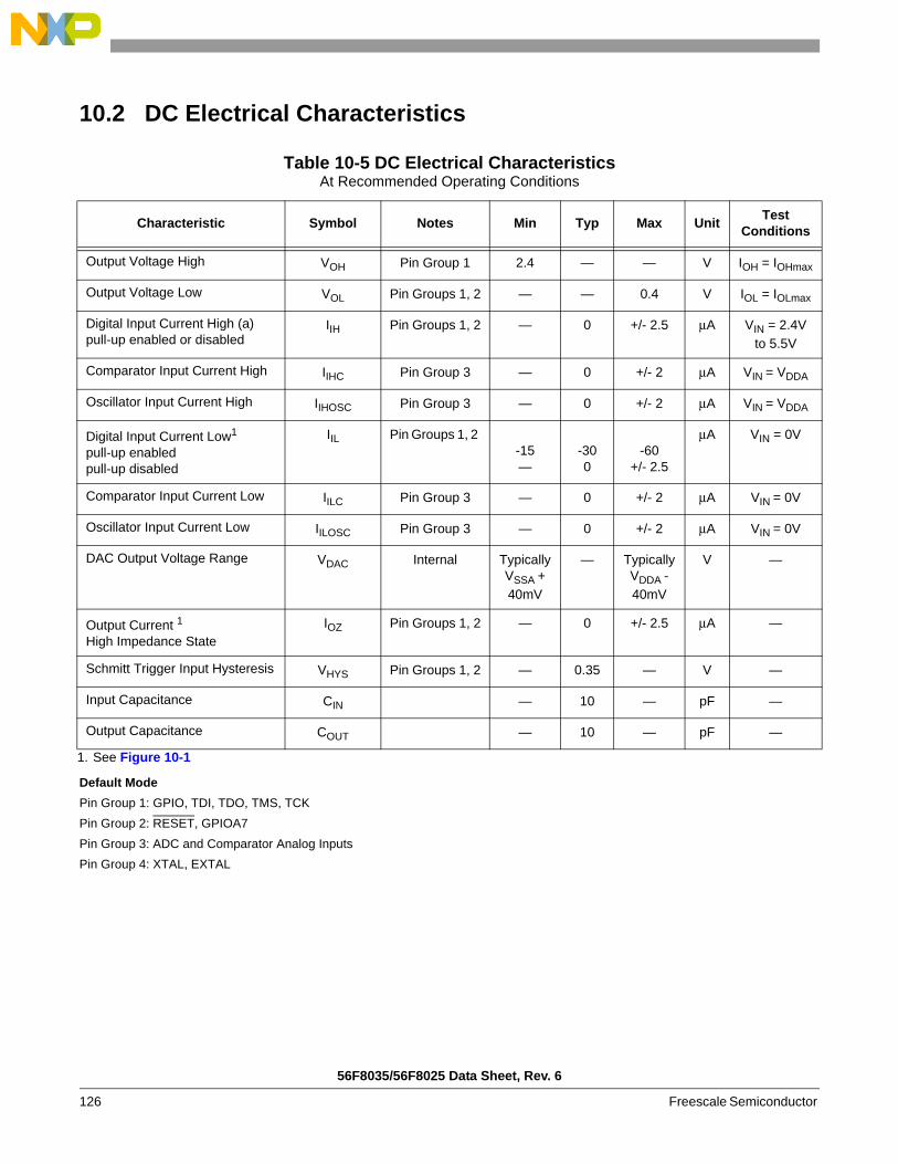
56F8035/56F8025 Data Sheet, Rev. 6
126 Freescale Semiconductor
10.2 DC Electrical Characteristics
Default ModePin Group 1: GPIO, TDI, TDO, TMS, TCKPin Group 2: RESET, GPIOA7Pin Group 3: ADC and Comparator Analog InputsPin Group 4: XTAL, EXTAL
Table 10-5 DC Electrical CharacteristicsAt Recommended Operating Conditions
Characteristic Symbol Notes Min Typ Max Unit Test Conditions
Output Voltage High VOH Pin Group 1 2.4 — — V IOH = IOHmax
Output Voltage Low VOL Pin Groups 1, 2 — — 0.4 V IOL = IOLmax
Digital Input Current High (a)pull-up enabled or disabled
IIH Pin Groups 1, 2 — 0 +/- 2.5 μA VIN = 2.4V to 5.5V
Comparator Input Current High IIHC Pin Group 3 — 0 +/- 2 μA VIN = VDDA
Oscillator Input Current High IIHOSC Pin Group 3 — 0 +/- 2 μA VIN = VDDA
Digital Input Current Low1
pull-up enabledpull-up disabled
1. See Figure 10-1
IIL Pin Groups 1, 2 -15—
-300
-60+/- 2.5
μA VIN = 0V
Comparator Input Current Low IILC Pin Group 3 — 0 +/- 2 μA VIN = 0V
Oscillator Input Current Low IILOSC Pin Group 3 — 0 +/- 2 μA VIN = 0V
DAC Output Voltage Range VDAC Internal Typically VSSA + 40mV
— Typically VDDA - 40mV
V —
Output Current 1High Impedance State
IOZ Pin Groups 1, 2 — 0 +/- 2.5 μA —
Schmitt Trigger Input Hysteresis VHYS Pin Groups 1, 2 — 0.35 — V —
Input Capacitance CIN — 10 — pF —
Output Capacitance COUT — 10 — pF —

DC Electrical Characteristics
56F8035/56F8025 Data Sheet, Rev. 6
Freescale Semiconductor 127
Figure 10-1 IIN/IOZ vs. VIN (Typical; Pull-Up Disabled)
Table 10-6 Current Consumption per Power Supply Pin
Mode ConditionsTypical @ 3.3V, 25°C Maximum@ 3.6V, 25°C
IDD1 IDDA IDD
1 IDDA
RUN 32MHz Device ClockRelaxation Oscillator onPLL powered onContinuous MAC instructions with fetches from Program FlashAll peripheral modules enabled. TMR and PWM using 1X ClockADC/DAC powered on and clockedComparator powered on
48mA 18.8mA — —
WAIT 32MHz Device Clock Relaxation Oscillator onPLL powered onProcessor Core in WAIT stateAll Peripheral modules enabled. TMR and PWM using 1X ClockADC/DAC/Comparator powered off
29mA 0μA — —
STOP 4MHz Device ClockRelaxation Oscillator onPLL powered offProcessor Core in STOP stateAll peripheral module and core clocks are offADC/DAC/Comparator powered off
5.4mA 0μA — —
2.0
0.0
- 2.0
- 4.0
- 6.0
- 8.0- 10.0
0.0 0.5 1.0 1.5 2.0 2.5 3.0 6.03.5 4.0 4.5 5.0 5.5
µA
Volt

56F8035/56F8025 Data Sheet, Rev. 6
128 Freescale Semiconductor
10.2.1 Voltage Regulator SpecificationsThe 56F8035/56F8025 has two on-chip regulators. One supplies the PLL and relaxation oscillator. It hasno external pins and therefore has no external characteristics which must be guaranteed (other than properoperation of the device). The second regulator supplies approximately 2.5V to the 56F8035/56F8025’score logic. This regulator requires an external 4.4µF, or greater, capacitor for proper operation. Ceramic
STANDBY > STOP 100kHz Device ClockRelaxation Oscillator in Standby modePLL powered offProcessor Core in STOP stateAll peripheral module and core clocks are offADC/DAC/Comparator powered offVoltage regulator in Standby mode
540μA 0μA 650μA 1μA
POWERDOWN Device Clock is offRelaxation Oscillator powered offPLL powered offProcessor Core in STOP stateAll peripheral module and core clocks are offADC /DAC/Comparator powered offVoltage Regulator in Standby mode
440μA 0μA 550μA 1μA
1. No Output SwitchingAll ports configured as inputsAll inputs LowNo DC Loads
Table 10-7 Power-On Reset Low-Voltage Parameters
Characteristic Symbol Min Typ Max Unit
Low-Voltage Interrupt for 3.3V supply1
1. When VDD drops below VEI3.3, an interrupt is generated.
VEI3.3 2.58 2.7 — V
Low-Voltage Interrupt for 2.5V supply2
2. When VDD drops below VEI32.5, an interrupt is generated.
VE12.5 — 2.15 — V
Low-Voltage Interrupt Recovery Hysteresis VEIH — 50 — mV
Power-On Reset3
3. Power-On Reset occurs whenever the internally regulated 2.5V digital supply drops below 1.8V. Whilepower is ramping up, this signal remains active for as long as the internal 2.5V is below 2.15V or the 3.3V1/O voltage is below 2.7V, no matter how long the ramp-up rate is. The internally regulated voltage istypically 100mV less than VDD during ramp-up until 2.5V is reached, at which time it self-regulates.
POR — 1.8 1.9 V
Table 10-6 Current Consumption per Power Supply Pin (Continued)
Mode ConditionsTypical @ 3.3V, 25°C Maximum@ 3.6V, 25°C
IDD1 IDDA IDD
1 IDDA

AC Electrical Characteristics
56F8035/56F8025 Data Sheet, Rev. 6
Freescale Semiconductor 129
and tantalum capacitors tend to provide better performance tolerances. The output voltage can bemeasured directly on the VCAP pin. The specifications for this regulator are shown in Table 10-8.
10.3 AC Electrical CharacteristicsTests are conducted using the input levels specified in Table 10-5. Unless otherwise specified,propagation delays are measured from the 50% to the 50% point, and rise and fall times are measuredbetween the 10% and 90% points, as shown in Figure 10-2.
Figure 10-2 Input Signal Measurement References
Figure 10-3 shows the definitions of the following signal states:
• Active state, when a bus or signal is driven, and enters a low impedance state• Tri-stated, when a bus or signal is placed in a high impedance state• Data Valid state, when a signal level has reached VOL or VOH
• Data Invalid state, when a signal level is in transition between VOL and VOH
Figure 10-3 Signal States
Table 10-8. Regulator Parameters
Characteristic Symbol Min Typical Max Unit
Short Circuit Current ISS — 450 650 mA
Short Circuit Tolerance(VCAP shorted to ground)
TRSC — — 30 minutes
VIH
VILFall Time
Input Signal
Note: The midpoint is VIL + (VIH – VIL)/2.
Midpoint1
Low High90%50%10%
Rise Time
Data Invalid State
Data1
Data2 Valid
DataTri-stated
Data3 Valid
Data2 Data3
Data1 Valid
Data Active Data Active

56F8035/56F8025 Data Sheet, Rev. 6
130 Freescale Semiconductor
10.4 Flash Memory Characteristics
10.5 External Clock Operation Timing
Figure 10-4 External Clock Timing
Table 10-9 Flash Timing Parameters
Characteristic Symbol Min Typ Max Unit
Program time1
1. There is additional overhead which is part of the programming sequence. See the 56F802x and 56F803x PeripheralReference Manual for details.
Tprog 20 — 40 μs
Erase time 2
2. Specifies page erase time. There are 512 bytes per page in the Program Flash memory.
Terase 20 — — ms
Mass erase time Tme 100 — — ms
Table 10-10 External Clock Operation Timing Requirements1
1. Parameters listed are guaranteed by design.
Characteristic Symbol Min Typ Max Unit
Frequency of operation (external clock driver)2
2. See Figure 10-4 for details on using the recommended connection of an external clock driver.
fosc 4 8 8 MHz
Clock Pulse Width3
3. The chip may not function if the high or low pulse width is smaller than 6.25ns.
tPW 6.25 — — ns
External Clock Input Rise Time4
4. External clock input rise time is measured from 10% to 90%.
trise — — 3 ns
External Clock Input Fall Time5
5. External clock input fall time is measured from 90% to 10%.
tfall — — 3 ns
ExternalClock
VIH
VIL
Note: The midpoint is VIL + (VIH – VIL)/2.
90%50%10%
90%50%10%
tPW tPWtfall trise
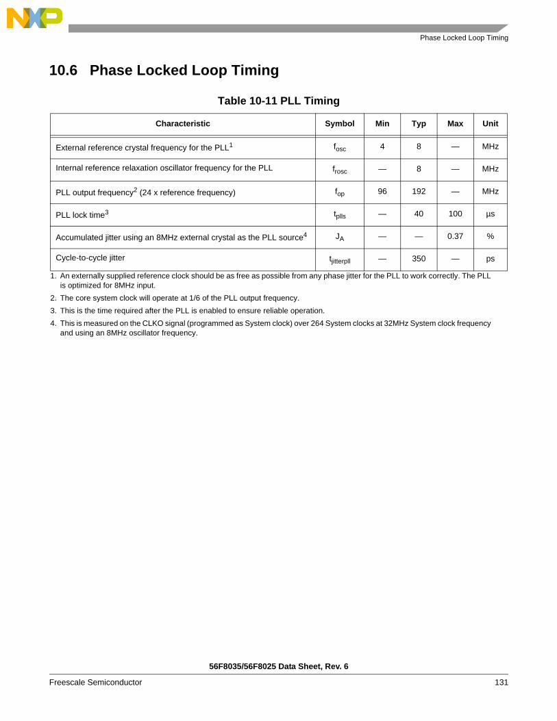
Phase Locked Loop Timing
56F8035/56F8025 Data Sheet, Rev. 6
Freescale Semiconductor 131
10.6 Phase Locked Loop Timing
Table 10-11 PLL Timing
Characteristic Symbol Min Typ Max Unit
External reference crystal frequency for the PLL1
1. An externally supplied reference clock should be as free as possible from any phase jitter for the PLL to work correctly. The PLLis optimized for 8MHz input.
fosc 4 8 — MHz
Internal reference relaxation oscillator frequency for the PLL frosc — 8 — MHz
PLL output frequency2 (24 x reference frequency)
2. The core system clock will operate at 1/6 of the PLL output frequency.
fop 96 192 — MHz
PLL lock time3
3. This is the time required after the PLL is enabled to ensure reliable operation.
tplls — 40 100 µs
Accumulated jitter using an 8MHz external crystal as the PLL source4
4. This is measured on the CLKO signal (programmed as System clock) over 264 System clocks at 32MHz System clock frequencyand using an 8MHz oscillator frequency.
JA — — 0.37 %
Cycle-to-cycle jitter tjitterpll — 350 — ps

56F8035/56F8025 Data Sheet, Rev. 6
132 Freescale Semiconductor
10.7 Relaxation Oscillator Timing
Figure 10-5 Relaxation Oscillator Temperature Variation (Typical) After Trim
Table 10-12 Relaxation Oscillator TimingCharacteristic Symbol Minimum Typical Maximum Unit
Relaxation Oscillator output frequency1
Normal ModeStandby Mode
1. Output frequency after factory trim value.
fop —8.05200
—MHzkHz
Relaxation Oscillator stabilization time2
2. This is the time required from Standby to Normal mode transition.
troscs — 1 3 ms
Cycle-to-cycle jitter. This is measured on the CLKO signal (programmed prescaler_clock) over 264 clocks3
3. JA is required to meet QSCI requirements.
tjitterrosc — 400 — ps
Minimum tuning step size — .08 — %
Maximum tuning step size — 40 — %
Variation over temperature -40°C to 150ºC4
4. See Figure 10-5
— +1.0 to -1.5 +3.0 to -3.0 %
Variation over temperature 0°C to 105ºC4 — 0 to +1 +2.0 to -2.0 %
8.16
8.08
8
7.92
7.84
175-25-50 0 50 75 100 125 15025
Degrees C (Junction)
MH
z

Reset, Stop, Wait, Mode Select, and Interrupt Timing
56F8035/56F8025 Data Sheet, Rev. 6
Freescale Semiconductor 133
10.8 Reset, Stop, Wait, Mode Select, and Interrupt Timing.
Figure 10-6 GPIO Interrupt Timing (Negative Edge-Sensitive)
Table 10-13 Reset, Stop, Wait, Mode Select, and Interrupt Timing1,2
1. In the formulas, T = system clock cycle and Tosc = oscillator clock cycle. For an operating frequency of 32MHz, T = 31.25ns. At8MHz (used during Reset and Stop modes), T = 125ns.
2. Parameters listed are guaranteed by design.
Characteristic Symbol Typical Min Typical Max Unit See Figure
Minimum RESET Assertion Duration tRA 4T — ns —
Minimum GPIO pin Assertion for Interrupt tIW 2T — ns 10-6
RESET deassertion to First Address Fetch3
3. During Power-On Reset, it is possible to use the 56F8035/56F8025 internal reset stretching circuitry to extend this period to2^21T.
tRDA 96TOSC + 64T 97TOSC + 65T ns —
Delay from Interrupt Assertion to Fetch of first instruction (exiting Stop)
tIF — 6T ns —
GPIO pin(Input)
TIW

56F8035/56F8025 Data Sheet, Rev. 6
134 Freescale Semiconductor
10.9 Serial Peripheral Interface (SPI) Timing
Table 10-14 SPI Timing1
Characteristic Symbol Min Max Unit See Figure
Cycle timeMasterSlave
tC12562.5
——
nsns
10-7, 10-8, 10-9, 10-10
Enable lead timeMasterSlave
tELD—31
——
nsns
10-10
Enable lag timeMasterSlave
tELG—
125——
nsns
10-10
Clock (SCK) high timeMaster Slave
tCH5031
——
nsns
10-7, 10-8, 10-9, 10-10
Clock (SCK) low timeMaster Slave
tCL5031
——
nsns
10-10
Data set-up time required for inputsMaster Slave
tDS200
——
nsns
10-7, 10-8, 10-9, 10-10
Data hold time required for inputsMaster Slave
tDH02
——
nsns
10-7, 10-8, 10-9, 10-10
Access time (time to data active from high-impedance state)Slave
tA4.8 15 ns
10-10
Disable time (hold time to high-impedance state)Slave
tD3.7 15.2 ns
10-10
Data Valid for outputsMasterSlave (after enable edge)
tDV——
4.520.4
nsns
10-7, 10-8, 10-9, 10-10
Data invalid MasterSlave
tDI00
——
nsns
10-7, 10-8, 10-9, 10-10
Rise timeMaster Slave
tR——
11.510.0
nsns
10-7, 10-8, 10-9, 10-10
Fall time Master Slave
tF——
9.79.0
nsns
10-7, 10-8, 10-9, 10-10

Serial Peripheral Interface (SPI) Timing
56F8035/56F8025 Data Sheet, Rev. 6
Freescale Semiconductor 135
Figure 10-7 SPI Master Timing (CPHA = 0)
1. Parameters listed are guaranteed by design.
SCLK (CPOL = 0)(Output)
SCLK (CPOL = 1)(Output)
MISO(Input)
MOSI(Output)
MSB in Bits 14–1 LSB in
tF
tC
tCL
tCL
tR
tRtF
tDS
tDH tCH
tDI tDV tDI(ref)
tR
Master MSB out Bits 14–1 Master LSB out
SS(Input)
tCH
SS is held High on master
tF

56F8035/56F8025 Data Sheet, Rev. 6
136 Freescale Semiconductor
Figure 10-8 SPI Master Timing (CPHA = 1)
SCLK (CPOL = 0)(Output)
SCLK (CPOL = 1)(Output)
MISO(Input)
MOSI(Output)
MSB in Bits 14–1 LSB in
tR
tC
tCL
tCL
tF
tCH
tDV(ref) tDV tDI(ref)
tRtF
Master MSB out Bits 14– 1 Master LSB out
SS(Input)
tCH
SS is held High on master
tDStDH
tDI
tR
tF

Serial Peripheral Interface (SPI) Timing
56F8035/56F8025 Data Sheet, Rev. 6
Freescale Semiconductor 137
Figure 10-9 SPI Slave Timing (CPHA = 0)
SCLK (CPOL = 0)(Input)
SCLK (CPOL = 1)(Input)
MISO(Output)
MOSI(Input)
Slave MSB out Bits 14–1
tC
tCL
tCL
tF
tCH
tDI
MSB in Bits 14–1 LSB in
SS(Input)
tCH
tDH
tR
tELG
tELD
tF
Slave LSB out
tDtA
tDS tDV tDI
tR

56F8035/56F8025 Data Sheet, Rev. 6
138 Freescale Semiconductor
Figure 10-10 SPI Slave Timing (CPHA = 1)
10.10 Quad Timer Timing
Table 10-15 Timer Timing1, 2
1. In the formulas listed, T = the clock cycle. For 32MHz operation, T = 31.25ns.2. Parameters listed are guaranteed by design.
Characteristic Symbol Min Max Unit See Figure
Timer input period PIN 2T + 6 — ns 10-11
Timer input high / low period PINHL 1T + 3 — ns 10-11
Timer output period POUT 125 — ns 10-11
Timer output high / low period POUTHL 50 — ns 10-11
SCLK (CPOL = 0)(Input)
SCLK (CPOL = 1)(Input)
MISO(Output)
MOSI(Input)
Slave MSB out Bits 14–1
tC
tCL
tCL
tCH
tDI
MSB in Bits 14–1 LSB in
SS(Input)
tCH
tDH
tF
tR
Slave LSB out
tDtA
tELD
tDV
tF
tR
tELG
tDV
tDS
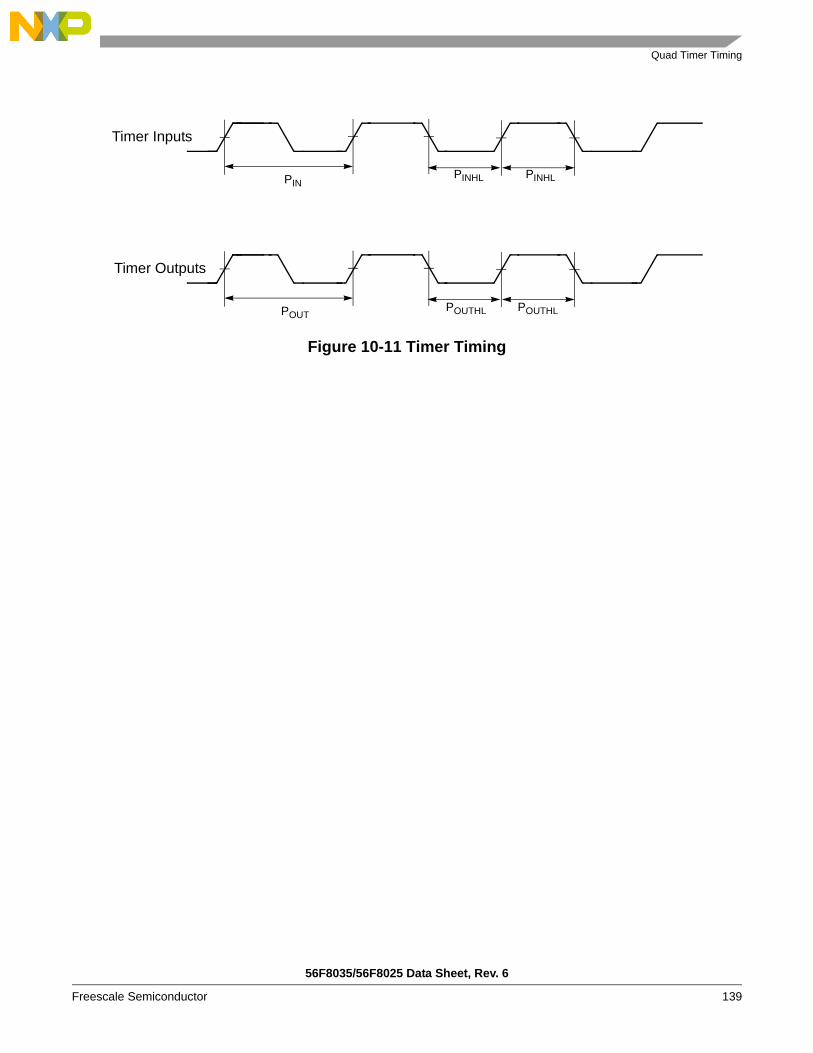
Quad Timer Timing
56F8035/56F8025 Data Sheet, Rev. 6
Freescale Semiconductor 139
Figure 10-11 Timer Timing
POUTPOUTHL POUTHL
PINPINHL PINHL
Timer Inputs
Timer Outputs

56F8035/56F8025 Data Sheet, Rev. 6
140 Freescale Semiconductor
10.11 Serial Communication Interface (SCI) Timing
Figure 10-12 RXD Pulse Width
Figure 10-13 TXD Pulse Width
Table 10-16 SCI Timing1
1. Parameters listed are guaranteed by design.
Characteristic Symbol Min Max Unit See Figure
Baud Rate2
2. fMAX is the frequency of operation of the system clock in MHz, which is 32MHz for the 56F8035/56F8025 device.
BR — (fMAX/16) Mbps —
RXD3 Pulse Width
3. The RXD pin in QSCI0 is named RXD0.
RXDPW 0.965/BR 1.04/BR ns 10-12
TXD4 Pulse Width
4. The TXD pin in QSCI0 is named TXD0.
TXDPW 0.965/BR 1.04/BR ns 10-13
LIN Slave Mode
Deviation of slave node clock from nominal clock rate before synchronization
FTOL_UNSYNCH -14 14 % —
Deviation of slave node clock relative to the master node clock after synchronization
FTOL_SYNCH -2 2 % —
Minimum break character length TBREAK 13 — Master node bit periods
—
11 — Slave node bit periods
—
RXDPW
RXD QSCI Receive
data pin(Input)
TXDPW
TXD QSCI Receive
data pin(Input)
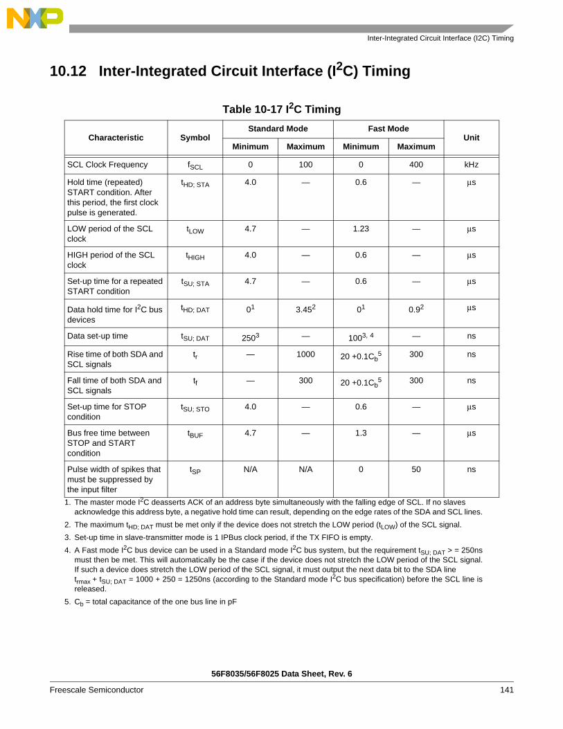
Inter-Integrated Circuit Interface (I2C) Timing
56F8035/56F8025 Data Sheet, Rev. 6
Freescale Semiconductor 141
10.12 Inter-Integrated Circuit Interface (I2C) Timing
Table 10-17 I2C Timing
Characteristic SymbolStandard Mode Fast Mode
UnitMinimum Maximum Minimum Maximum
SCL Clock Frequency fSCL 0 100 0 400 kHz
Hold time (repeated) START condition. After this period, the first clock pulse is generated.
tHD; STA 4.0 — 0.6 — μs
LOW period of the SCL clock
tLOW 4.7 — 1.23 — μs
HIGH period of the SCL clock
tHIGH 4.0 — 0.6 — μs
Set-up time for a repeated START condition
tSU; STA 4.7 — 0.6 — μs
Data hold time for I2C bus devices
tHD; DAT 01
1. The master mode I2C deasserts ACK of an address byte simultaneously with the falling edge of SCL. If no slaves acknowledge this address byte, a negative hold time can result, depending on the edge rates of the SDA and SCL lines.
3.452
2. The maximum tHD; DAT must be met only if the device does not stretch the LOW period (tLOW) of the SCL signal.
01 0.92 μs
Data set-up time tSU; DAT 2503
3. Set-up time in slave-transmitter mode is 1 IPBus clock period, if the TX FIFO is empty.
— 1003, 4
4. A Fast mode I2C bus device can be used in a Standard mode I2C bus system, but the requirement tSU; DAT > = 250nsmust then be met. This will automatically be the case if the device does not stretch the LOW period of the SCL signal.If such a device does stretch the LOW period of the SCL signal, it must output the next data bit to the SDA line trmax + tSU; DAT = 1000 + 250 = 1250ns (according to the Standard mode I2C bus specification) before the SCL line isreleased.
— ns
Rise time of both SDA and SCL signals
tr — 1000 20 +0.1Cb5
5. Cb = total capacitance of the one bus line in pF
300 ns
Fall time of both SDA and SCL signals
tf — 300 20 +0.1Cb5 300 ns
Set-up time for STOP condition
tSU; STO 4.0 — 0.6 — μs
Bus free time between STOP and START condition
tBUF 4.7 — 1.3 — μs
Pulse width of spikes that must be suppressed by the input filter
tSP N/A N/A 0 50 ns

56F8035/56F8025 Data Sheet, Rev. 6
142 Freescale Semiconductor
Figure 10-14 Timing Definition for Fast and Standard Mode Devices on the I2C Bus
SDA
SCL
tHD; STAtHD; DAT
tLOWtSU; DAT
tHIGH
tSU; STASR P SS
tHD; STA tSP
tSU; STO
tBUFtf trtf
tr
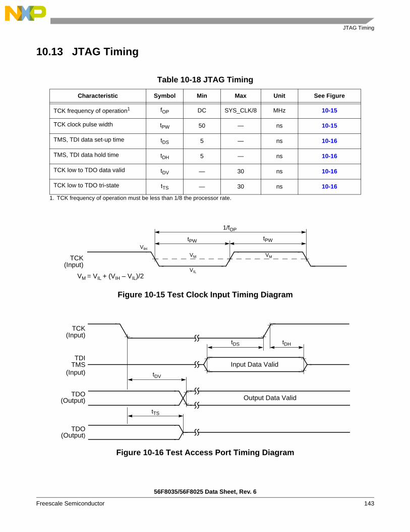
JTAG Timing
56F8035/56F8025 Data Sheet, Rev. 6
Freescale Semiconductor 143
10.13 JTAG Timing
Figure 10-15 Test Clock Input Timing Diagram
Figure 10-16 Test Access Port Timing Diagram
Table 10-18 JTAG Timing
Characteristic Symbol Min Max Unit See Figure
TCK frequency of operation1
1. TCK frequency of operation must be less than 1/8 the processor rate.
fOP DC SYS_CLK/8 MHz 10-15
TCK clock pulse width tPW 50 — ns 10-15
TMS, TDI data set-up time tDS 5 — ns 10-16
TMS, TDI data hold time tDH 5 — ns 10-16
TCK low to TDO data valid tDV — 30 ns 10-16
TCK low to TDO tri-state tTS — 30 ns 10-16
TCK(Input)
VM
VILVM = VIL + (VIH – VIL)/2
tPW
1/fOP
tPW
VM
VIH
Input Data Valid
Output Data Valid
tDS tDH
tDV
tTS
TCK(Input)
TDI
(Input)
TDO(Output)
TDO(Output)
TMS
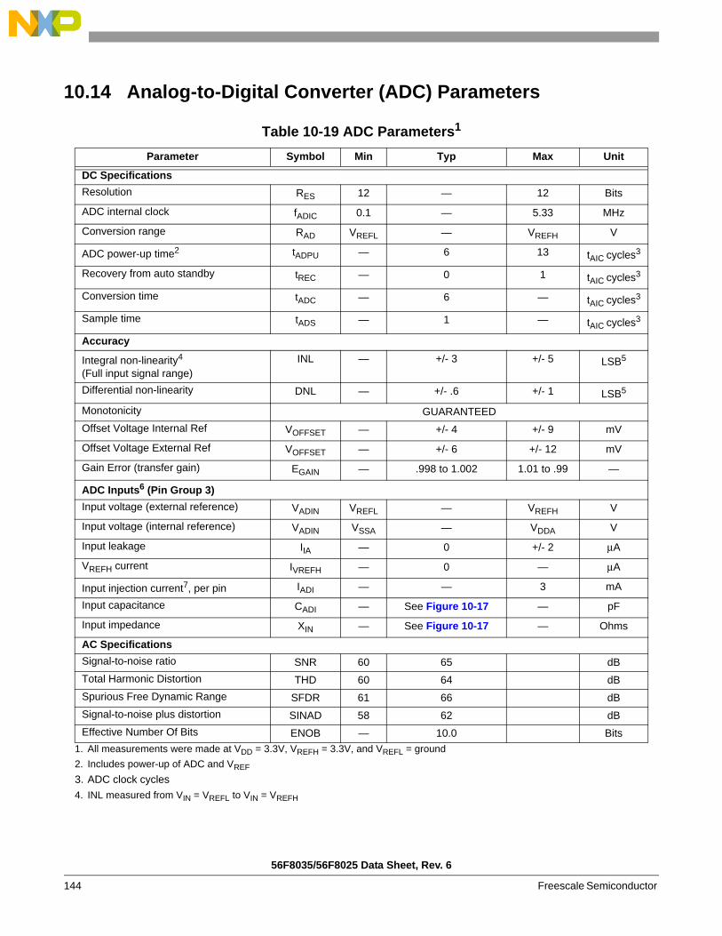
56F8035/56F8025 Data Sheet, Rev. 6
144 Freescale Semiconductor
10.14 Analog-to-Digital Converter (ADC) Parameters
Table 10-19 ADC Parameters1
1. All measurements were made at VDD = 3.3V, VREFH = 3.3V, and VREFL = ground
Parameter Symbol Min Typ Max Unit
DC SpecificationsResolution RES 12 — 12 Bits
ADC internal clock fADIC 0.1 — 5.33 MHz
Conversion range RAD VREFL — VREFH V
ADC power-up time2
2. Includes power-up of ADC and VREF
tADPU — 6 13 tAIC cycles3
3. ADC clock cycles
Recovery from auto standby tREC — 0 1 tAIC cycles3
Conversion time tADC — 6 — tAIC cycles3
Sample time tADS — 1 — tAIC cycles3
Accuracy
Integral non-linearity4
(Full input signal range)
4. INL measured from VIN = VREFL to VIN = VREFH
INL — +/- 3 +/- 5 LSB5
Differential non-linearity DNL — +/- .6 +/- 1 LSB5
Monotonicity GUARANTEEDOffset Voltage Internal Ref VOFFSET — +/- 4 +/- 9 mV
Offset Voltage External Ref VOFFSET — +/- 6 +/- 12 mV
Gain Error (transfer gain) EGAIN — .998 to 1.002 1.01 to .99 —
ADC Inputs6 (Pin Group 3)Input voltage (external reference) VADIN VREFL — VREFH V
Input voltage (internal reference) VADIN VSSA — VDDA V
Input leakage IIA — 0 +/- 2 μA
VREFH current IVREFH — 0 — μA
Input injection current7, per pin IADI — — 3 mA
Input capacitance CADI — See Figure 10-17 — pF
Input impedance XIN — See Figure 10-17 — Ohms
AC SpecificationsSignal-to-noise ratio SNR 60 65 dBTotal Harmonic Distortion THD 60 64 dBSpurious Free Dynamic Range SFDR 61 66 dBSignal-to-noise plus distortion SINAD 58 62 dBEffective Number Of Bits ENOB — 10.0 Bits

Equivalent Circuit for ADC Inputs
56F8035/56F8025 Data Sheet, Rev. 6
Freescale Semiconductor 145
10.15 Equivalent Circuit for ADC InputsFigure 10-17 illustrates the ADC input circuit during sample and hold. S1 and S2 are always open/closedat the same time that S3 is closed/open. When S1/S2 are closed and S3 is open, one input of the sampleand hold circuit moves to (VREFHx - VREFLx) / 2, while the other charges to the analog input voltage. Whenthe switches are flipped, the charge on C1 and C2 are averaged via S3, with the result that a single-endedanalog input is switched to a differential voltage centered about (VREFHx - VREFLx) / 2. The switchesswitch on every cycle of the ADC clock (open one-half ADC clock, closed one-half ADC clock). Note thatthere are additional capacitances associated with the analog input pad, routing, etc., but these do not filterinto the S/H output voltage, as S1 provides isolation during the charge-sharing phase.
One aspect of this circuit is that there is an on-going input current, which is a function of the analog inputvoltage, VREF, and the ADC clock frequency.
1. Parasitic capacitance due to package, pin-to-pin and pin-to-package base coupling; 1.8pF2. Parasitic capacitance due to the chip bond pad, ESD protection devices and signal routing; 2.04pF3. Equivalent resistance for the channel select mux; 100 ohms4. Sampling capacitor at the sample and hold circuit. Capacitor C1 is normally disconnected from the input and is only
connected to it at sampling time; 1.4pF
Figure 10-17 Equivalent Circuit for A/D Loading
5. LSB = Least Significant Bit = 0.806mV6. Pin groups are detailed following Table 10-1.7. The current that can be injected or sourced from an unselected ADC signal input without impacting the performance of the
ADC.
1 2
3Analog Input 4S1
S2
S3
C1
C2
S/H
C1 = C2 = 1pF(VREFHx - VREFL x) / 2
125Ω ESD Resistor
8pF noise damping capacitor

56F8035/56F8025 Data Sheet, Rev. 6
146 Freescale Semiconductor
10.16 Comparator (CMP) Parameters
10.17 Digital-to-Analog Converter (DAC) Parameters
Table 10-20 CMP Parameters
Characteristic Conditions/Comments Symbol Min Typ Max Unit
Input Offset Voltage1
1. No guaranteed specification within 0.1V of VDDA or VSSA
Within range of VDDA - .1V to VSSA + .1V
VOFFSET — ±10 ±35 mV
Input Propagation Delay tPD — 35 45 ns
Power-up time tCPU — TBD TBD
Table 10-21 DAC ParametersParameter Conditions/Comments Symbol Min Typ Max Unit
DC SpecificationsResolution 12 12 bits
Conversion time TBD — 2 µS
Conversion rate TBD — 500.000 conv/sec
Power-up time Time from release of PWRDWN signal until DACOUT signal is valid
tDAPU — — 11 µS
Accuracy
Integral non-linearity1 Range of input digital words:410 to 3891 ($19A - $F33)5% to 95% of full range
INL — +/- 3 +/- 8.0 LSB2
Differential non-linearity1 Range of input digital words:410 to 3891 ($19A - $F33)5% to 95% of full range
DNL — +/- .8 < - 1 LSB2
Monotonicity > 6 sigma monotonicity, < 3.4 ppm non-monotonicity
guaranteed —
Offset error1 Range of input digital words:410 to 3891 ($19A - $F33)5% to 95% of full range
VOFFSET — +/- 25 +/- 40 mV
Gain error1 Range of input digital words:410 to 3891 ($19A - $F33)5% to 95% of full range
EGAIN — +/- .5 +/- 1.5 %
DAC OutputOutput voltage range Within 40mV of either VREFLX or
VREFHX
VOUT VREFLX +.04V
— VREFHX- .04V
V
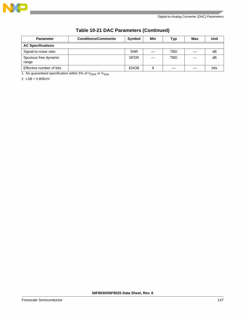
Digital-to-Analog Converter (DAC) Parameters
56F8035/56F8025 Data Sheet, Rev. 6
Freescale Semiconductor 147
AC SpecificationsSignal-to-noise ratio SNR — TBD — dB
Spurious free dynamic range
SFDR — TBD — dB
Effective number of bits ENOB 9 — — bits1. No guaranteed specification within 5% of VDDA or VSSA
2. LSB = 0.806mV
Table 10-21 DAC Parameters (Continued)Parameter Conditions/Comments Symbol Min Typ Max Unit

56F8035/56F8025 Data Sheet, Rev. 6
148 Freescale Semiconductor
10.18 Power ConsumptionSee Section 10.1 for a list of IDD requirements for the 56F8035/56F8025. This section provides additionaldetail which can be used to optimize power consumption for a given application.
Power consumption is given by the following equation:
A, the internal [static component], is comprised of the DC bias currents for the oscillator, leakage currents,PLL, and voltage references. These sources operate independently of processor state or operatingfrequency.
B, the internal [state-dependent component], reflects the supply current required by certain on-chipresources only when those resources are in use. These include RAM, Flash memory and the ADCs.
C, the internal [dynamic component], is classic C*V2*F CMOS power dissipation corresponding to the56800E core and standard cell logic.
D, the external [dynamic component], reflects power dissipated on-chip as a result of capacitive loadingon the external pins of the chip. This is also commonly described as C*V2*F, although simulations on twoof the I/O cell types used on the 56800E reveal that the power-versus-load curve does have a non-zeroY-intercept.
Power due to capacitive loading on output pins is (first order) a function of the capacitive load andfrequency at which the outputs change. Table 10-22 provides coefficients for calculating power dissipatedin the I/O cells as a function of capacitive load. In these cases:
TotalPower = Σ((Intercept + Slope*Cload)*frequency/10MHz)
where:
• Summation is performed over all output pins with capacitive loads• TotalPower is expressed in mW
Total power = A: internal [static component]+B: internal [state-dependent component]+C: internal [dynamic component]+D: external [dynamic component]+E: external [static component]
Table 10-22 I/O Loading Coefficients at 10MHz
Intercept Slope
8mA drive 1.3 0.11mW / pF
4mA drive 1.15mW 0.11mW / pF
56F8035/56F8025 Package and Pin-Out Information
56F8035/56F8025 Data Sheet, Rev. 6
Freescale Semiconductor 149
• Cload is expressed in pFBecause of the low duty cycle on most device pins, power dissipation due to capacitive loads was foundto be fairly low when averaged over a period of time.
E, the external [static component], reflects the effects of placing resistive loads on the outputs of thedevice. Sum the total of all V2/R or IV to arrive at the resistive load contribution to power. Assume V = 0.5for the purposes of these rough calculations. For instance, if there is a total of eight PWM outputs driving10mA into LEDs, then P = 8*.5*.01 = 40mW.
In previous discussions, power consumption due to parasitics associated with pure input pins is ignored,as it is assumed to be negligible.
Part 11 Packaging
11.1 56F8035/56F8025 Package and Pin-Out Information This section contains package and pin-out information for the 56F8035/56F8025. This device comes in a44-pin Low-profile Quad Flat Pack (LQFP). Figure 11-1 shows the package outline, Figure 11-2 showsthe mechanical parameters and Table 11-1 lists the pin-out.

56F8035/56F8025 Data Sheet, Rev. 6
150 Freescale Semiconductor
Figure 11-1 Top View, 56F8035/56F8025 44-Pin LQFP Package
ORIENTATIONMARK
PIN 12
PIN 34
PIN 23
PIN 1
GPIOB6 / RXD0 / SDA / CLKIN
GPIOB1 / SS0 / SDA
GPIOB7 / TXD0 / SCL
GPIOB5 / TA1 / FAULT3 / CLKIN
GPIOA9 / FAULT2 / TA3 / CMPBI1
GPIOA11 / CMPBI2
GPIOC4 / ANB0 & CMPBI3
GPIOC5 / ANB1
GPIOC6 / ANB2 / VREFHB
GPIOC7 / ANB3 / VREFLB
VDDA
V SSA
GPI
OC
3 / A
NA
3 / V
RE
FLA
GPI
OC
2 / A
NA
2 /
VR
EFH
A
GPI
OC
1 / A
NA
1
GPI
OC
0 / A
NA
0 &
CM
PA
I3
V SS
V CA
P
TCK
/ G
PIO
D2
RES
ET /
GP
IOA
7
GPI
OB
3 / M
OS
I0 /
TA3
/ PS
RC
1
GPI
OB
10 /
CM
PA
O
GPIOA3 / PWM3
GPIOA2 / PWM2
GPIOA4 / PWM4 / TA2 / FAULT1
GPIOB0 / SCLK0 / SCL
VDD
VSS
GPIOA5 / PWM5 / TA3 / FAULTA2
GPIOA8 / FAULTA1 / TA2 / CMPAI1
GPIOA10 / CMPAI2
GPIOA6 / FAULT0 / TA0
GPIOB2 / MISO0 / TA2 / PSRC0
TDO
/ G
PIO
D1
TMS
/ GP
IOD
3
GPI
OB
11 /
CM
PB
O
TDI /
GP
IOD
0
GPI
OA
0 / P
WM
0
GPI
OA
1 / P
WM
1
GPI
OD
4 / E
XTA
L
GPI
OD
5 / X
TAL
/ CLK
IN
V SS
V DD
V CA
P

56F8035/56F8025 Package and Pin-Out Information
56F8035/56F8025 Data Sheet, Rev. 6
Freescale Semiconductor 151
Table 11-1 56F8035/56F8025 44-Pin LQFP Package Identification by Pin Number1
1. Alternate signals are in italic
Pin # Signal Name Pin
# Signal Name Pin # Signal Name Pin
# Signal Name
1 GPIOB6RXD0 / SDA / CLKIN
12 VSSA 23 GPIOB2MISO0 / TA2 / PSRC0
34 VCAP
2 GPIOB1SS0 / SDA
13 GPIOC3ANA3 / VREFLA
24 GPIOA6FAULT0 / TA0
35 VDD
3 GPIOB7TXD0 / SCL
14 GPIOC2ANA2 / VREFHA
25 GPIOA10CMPAI2
36 VSS
4 GPIOB5TA1 / FAULT3 / CLKIN
15 GPIOC1ANA1
26 GPIOA8 FAULT1 / TA2 /
CMPAI1
37 GPIOD5XTAL / CLKIN
5 GPIOA9FAULT2 / TA3 /
CMPBI1
16 GPIOC0ANA0 & CMPAI3
27 GPIOA5PWM5 / TA3 / FAULT2
38 GPIOD4EXTAL
6 GPIOA11CMPBI2
17 VSS 28 VSS 39 GPIOA1PWM1
7 GPIOC4ANB0 &CMPBI3
18 VCAP 29 VDD 40 GPIOA0 PWM0
8 GPIOC5ANB1
19 TCIGPIOD2
30 GPIOB0SCLK0 / SCL
41 TDIGPIOD0
9 GPIOC6ANB2 / VREFHB
20 GPIOB10CMPAO
31 GPIOA4PWM4 / TA2 / FAULT1
42 GPIOB11CMPBO
10 GPIOC7ANB3 / VREFLB
21 RESETGPIOA7
32 GPIOA2PWM2
43 TMSGPIOD3
11 VDDA 22 GPIOB3MOSI0 / TA3 /
PSRC1
33 GPIOA3PWM3
44 TDOGPIOD1
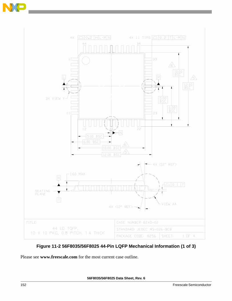
56F8035/56F8025 Data Sheet, Rev. 6
152 Freescale Semiconductor
Figure 11-2 56F8035/56F8025 44-Pin LQFP Mechanical Information (1 of 3)
Please see www.freescale.com for the most current case outline.

56F8035/56F8025 Package and Pin-Out Information
56F8035/56F8025 Data Sheet, Rev. 6
Freescale Semiconductor 153
Figure 11-3 56F8035/56F8025 44-Pin LQFP Mechanical Information (2 of 3)
Please see www.freescale.com for the most current case outline.

56F8035/56F8025 Data Sheet, Rev. 6
154 Freescale Semiconductor
Figure 11-4 56F8035/56F8025 44-Pin LQFP Mechanical Information (3 of 3)
Please see www.freescale.com for the most current case outline.

Thermal Design Considerations
56F8035/56F8025 Data Sheet, Rev. 6
Freescale Semiconductor 155
Part 12 Design Considerations
12.1 Thermal Design ConsiderationsAn estimation of the chip junction temperature, TJ, can be obtained from the equation:
TJ = TA + (RθJΑ x PD)where:
The junction-to-ambient thermal resistance is an industry-standard value that provides a quick and easyestimation of thermal performance. Unfortunately, there are two values in common usage: the valuedetermined on a single-layer board and the value obtained on a board with two planes. For packages suchas the PBGA, these values can be different by a factor of two. Which value is closer to the applicationdepends on the power dissipated by other components on the board. The value obtained on a single layerboard is appropriate for the tightly packed printed circuit board. The value obtained on the board with theinternal planes is usually appropriate if the board has low-power dissipation and the components are wellseparated.
When a heat sink is used, the thermal resistance is expressed as the sum of a junction-to-case thermalresistance and a case-to-ambient thermal resistance:
RθJA = RθJC + RθCAwhere:
RθJC is device related and cannot be influenced by the user. The user controls the thermal environment tochange the case to ambient thermal resistance, RθCA. For instance, the user can change the size of the heatsink, the air flow around the device, the interface material, the mounting arrangement on printed circuitboard, or change the thermal dissipation on the printed circuit board surrounding the device.
To determine the junction temperature of the device in the application when heat sinks are not used, theThermal Characterization Parameter (ΨJT) can be used to determine the junction temperature with ameasurement of the temperature at the top center of the package case using the following equation:
TJ = TT + (ΨJT x PD)where:
TA = Ambient temperature for the package (oC)RθJΑ = Junction-to-ambient thermal resistance (oC/W)PD = Power dissipation in the package (W)
RθJA = Package junction-to-ambient thermal resistance (°C/W)RθJC = Package junction-to-case thermal resistance (°C/W)RθCA = Package case-to-ambient thermal resistance (°C/W)
TT = Thermocouple temperature on top of package (oC)ΨJT = Thermal characterization parameter (oC/W)PD = Power dissipation in package (W)

56F8035/56F8025 Data Sheet, Rev. 6
156 Freescale Semiconductor
The thermal characterization parameter is measured per JESD51-2 specification using a 40-gauge type Tthermocouple epoxied to the top center of the package case. The thermocouple should be positioned sothat the thermocouple junction rests on the package. A small amount of epoxy is placed over thethermocouple junction and over about 1mm of wire extending from the junction. The thermocouple wireis placed flat against the package case to avoid measurement errors caused by cooling effects of thethermocouple wire.
When heat sink is used, the junction temperature is determined from a thermocouple inserted at theinterface between the case of the package and the interface material. A clearance slot or hole is normallyrequired in the heat sink. Minimizing the size of the clearance is important to minimize the change inthermal performance caused by removing part of the thermal interface to the heat sink. Because of theexperimental difficulties with this technique, many engineers measure the heat sink temperature and thenback-calculate the case temperature using a separate measurement of the thermal resistance of theinterface. From this case temperature, the junction temperature is determined from the junction-to-casethermal resistance.
12.2 Electrical Design Considerations
Use the following list of considerations to assure correct operation of the 56F8035/56F8025:
• Provide a low-impedance path from the board power supply to each VDD pin on the 56F8035/56F8025 and from the board ground to each VSS (GND) pin
• The minimum bypass requirement is to place 0.01–0.1µF capacitors positioned as close as possible to the package supply pins. The recommended bypass configuration is to place one bypass capacitor on each of the VDD/VSS pairs, including VDDA/VSSA. Ceramic and tantalum capacitors tend to provide better tolerances.
• Ensure that capacitor leads and associated printed circuit traces that connect to the chip VDD and VSS (GND) pins are as short as possible
• Bypass the VDD and VSS with approximately 100µF, plus the number of 0.1µF ceramic capacitors• PCB trace lengths should be minimal for high-frequency signals
CAUTION
This device contains protective circuitry to guardagainst damage due to high static voltage or electricalfields. However, normal precautions are advised toavoid application of any voltages higher thanmaximum-rated voltages to this high-impedance circuit.Reliability of operation is enhanced if unused inputs aretied to an appropriate voltage level.
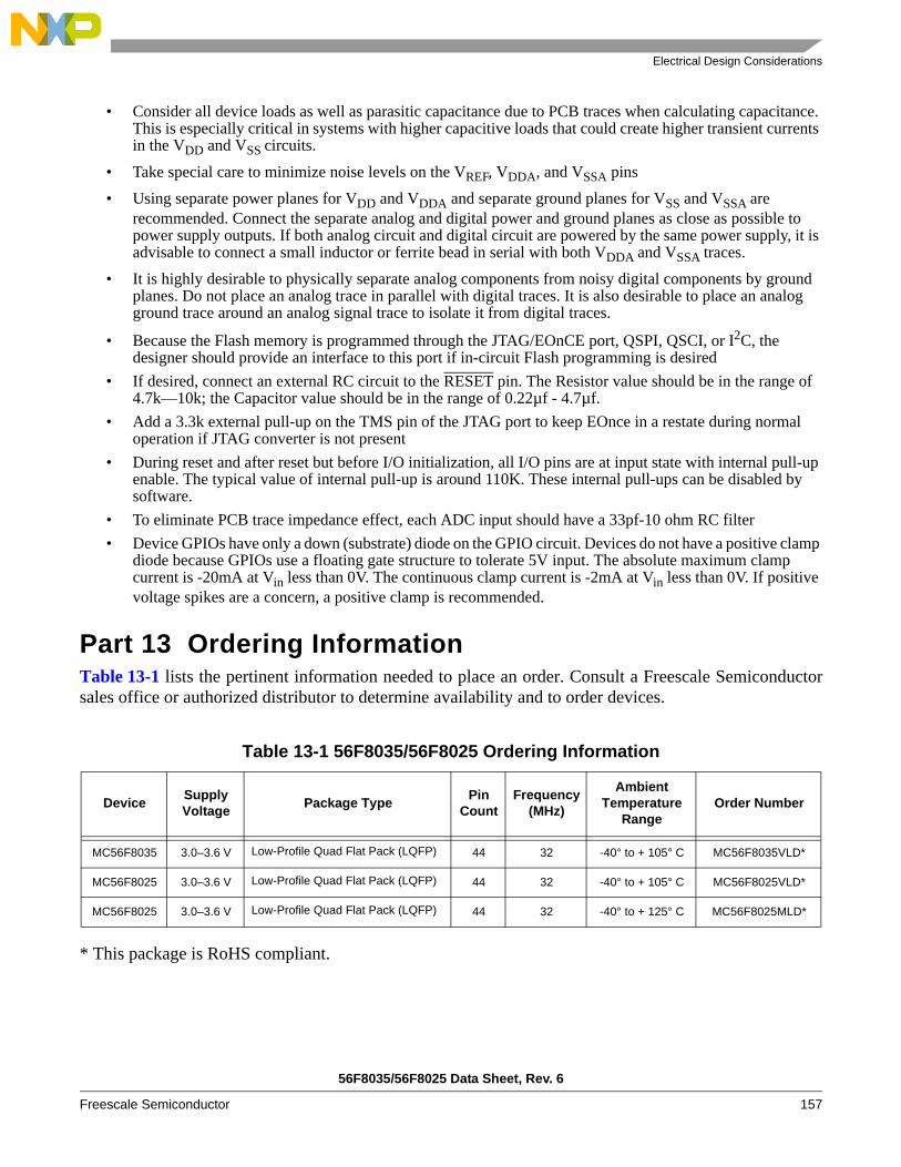
Electrical Design Considerations
56F8035/56F8025 Data Sheet, Rev. 6
Freescale Semiconductor 157
• Consider all device loads as well as parasitic capacitance due to PCB traces when calculating capacitance. This is especially critical in systems with higher capacitive loads that could create higher transient currents in the VDD and VSS circuits.
• Take special care to minimize noise levels on the VREF, VDDA, and VSSA pins• Using separate power planes for VDD and VDDA and separate ground planes for VSS and VSSA are
recommended. Connect the separate analog and digital power and ground planes as close as possible to power supply outputs. If both analog circuit and digital circuit are powered by the same power supply, it is advisable to connect a small inductor or ferrite bead in serial with both VDDA and VSSA traces.
• It is highly desirable to physically separate analog components from noisy digital components by ground planes. Do not place an analog trace in parallel with digital traces. It is also desirable to place an analog ground trace around an analog signal trace to isolate it from digital traces.
• Because the Flash memory is programmed through the JTAG/EOnCE port, QSPI, QSCI, or I2C, the designer should provide an interface to this port if in-circuit Flash programming is desired
• If desired, connect an external RC circuit to the RESET pin. The Resistor value should be in the range of 4.7k—10k; the Capacitor value should be in the range of 0.22µf - 4.7µf.
• Add a 3.3k external pull-up on the TMS pin of the JTAG port to keep EOnce in a restate during normal operation if JTAG converter is not present
• During reset and after reset but before I/O initialization, all I/O pins are at input state with internal pull-up enable. The typical value of internal pull-up is around 110K. These internal pull-ups can be disabled by software.
• To eliminate PCB trace impedance effect, each ADC input should have a 33pf-10 ohm RC filter• Device GPIOs have only a down (substrate) diode on the GPIO circuit. Devices do not have a positive clamp
diode because GPIOs use a floating gate structure to tolerate 5V input. The absolute maximum clamp current is -20mA at Vin less than 0V. The continuous clamp current is -2mA at Vin less than 0V. If positive voltage spikes are a concern, a positive clamp is recommended.
Part 13 Ordering InformationTable 13-1 lists the pertinent information needed to place an order. Consult a Freescale Semiconductorsales office or authorized distributor to determine availability and to order devices.
* This package is RoHS compliant.
Table 13-1 56F8035/56F8025 Ordering Information
Device SupplyVoltage Package Type Pin
CountFrequency
(MHz)
AmbientTemperature
RangeOrder Number
MC56F8035 3.0–3.6 V Low-Profile Quad Flat Pack (LQFP) 44 32 -40° to + 105° C MC56F8035VLD*
MC56F8025 3.0–3.6 V Low-Profile Quad Flat Pack (LQFP) 44 32 -40° to + 105° C MC56F8025VLD*
MC56F8025 3.0–3.6 V Low-Profile Quad Flat Pack (LQFP) 44 32 -40° to + 125° C MC56F8025MLD*

56F8035/56F8025 Data Sheet, Rev. 6
158 Freescale Semiconductor
Part 14 Appendix Register acronyms are revised from previous device data sheets to provide a cleaner register description.A cross reference to legacy and revised acronyms are provided in the following table.
Table 14-1 Legacy and Revised Acronyms
Register Name
Peripheral ReferenceManual
Data SheetProcessor Expert
Acronym
MemoryAddress
NewAcronym
LegacyAcronym
NewAcronym
LegacyAcronym
Start End
Analog-to-Digital Converter (ADC) Module
Control 1 Register CTRL1 ADCR1 ADC_CTRL1 ADC_ADCR1 ADC_ADCR1 0xF080
Control 2 Register CTRL2 ADCR2 ADC_CTRL2 ADC_ADCR2 ADC_ADCR2 0xF081
Zero Crossing Control Register
ZXCTRL ADZCC ADC_ZXCTRL ADC_ADZCC ADC_ADZCC 0xF082
Channel List 1 Register
CLIST1 ADLST1 ADC_CLIST1 ADC_ADLST1 ADC_ADLST1 0xF083
Channel List 2 Register
CLIST2 ADLST2 ADC_CLIST2 ADC_ADLST2 ADC_ADLST2 0xF084
Channel List 3 Register
CLIST3 ADC_CLIST3 ADC_ADCLST3 ADC_ADCLST3 0xF085
Channel List 4 Register
CLIST4 ADC_CLIST4 ADC_ADCLST4 ADC_ADCLST4 0xF086
Sample Disable Register
SDIS ADSDIS ADC_SDIS ADC_ADSDIS ADC_ADSDIS 0xF087
Status Register STAT ADSTAT ADC_STAT ADC_ADSTAT ADC_ADSTAT 0xF088
Conversion Ready Register
RDY ADC_CNRDY ADC_ADCNRDY ADC_ADCNRDY 0xF089
Limit Status Register LIMSTAT ADLSTAT ADC_LIMSTAT ADC_ADLSTAT ADC_ADLSTAT 0xF08A
Zero Crossing Status Register
ZXSTAT ADZCSTAT ADC_ZXSTAT ADC_ADZCSTAT ADC_ADZCSTAT 0xF08B
Result 0-7 Registers RSLT0-7 ADRSLT0-7 ADC_RSLT0-7 ADC_ADRSLT0-7 ADC_ADRSLT0-7 0xF08C 0XF093
Result 8-15 Registers RSLT8-15 ADC_RSLT8-15 ADC_ADRSLT8-15 ADC_ADRSLT8-15 0xF094 0XF09B
Low Limit 0-7 Registers
LOLIM0-7 ADLLMT0-7 ADC_LOLIM0-7 ADC_ADLLMT0-7 ADC_ADLLMT0-7 0XF09C 0XF0A3
High Limit 0-7 Registers
HILIM0-7 ADHLMT0-7 ADC_HILIM0-7 ADC_ADHLMT0-7 ADC_ADHLMT0-7 0XF0A4 0XF0AB
Offset 0-7 Registers OFFST0-7 ADOFS0-7 ADC_OFFST0-7 ADC_ADOFS0-7 ADC_ADOFS0-7 0XF0AC 0XF0B3
Power Control Register
PWR ADPOWER ADC_PWR ADC_ADPOWER ADC_ADPOWER 0XF0B4
Calibration Register CAL ADC_CAL ADC_ADCAL ADC_ADCAL 0XF0B5
Computer Operating Properly (COP) Module
Control Register CTRL COPCTL COP_CTRL COPCTL COPCTL 0XF120
Timeout Register TOUT COPTO COP_TOUT COPTO COPTO 0XF121
Counter Register CNTR COPCTR COP_CNTR COPCTR COPCTR 0XF122

Electrical Design Considerations
56F8035/56F8025 Data Sheet, Rev. 6
Freescale Semiconductor 159
Inter-Integrated Circuit Interface (I2C) Module
Control Register CTRL IBCR I2C_CTRL I2C_IBCR I2C_IBCR 0xF280
Target Address Register
TAR I2C_TAR I2CTAR I2C_TAR 0xF282
Slave Address Register
SAR I2C_SAR I2CSAR I2C_SAR 0xF242
Data Buffer & Command Register
DATA I2C_DATA I2C_DATACMD I2C_DATACMD 0xF288
Standard Speed Clock SCL High Count Register
SSHCNT I2C_SS_SCL_HCNT I2C_SS_SCLHCNT I2C_SS_SCLHCNT 0xF28A
Standard Speed Clock SCL Low Count Register
SSLCNT I2C_SS_SCL_LCNT I2C_SS_SCLLCNT I2C_SS_SCLLCNT 0xF28C
Fast Speed Clock SCL High Count Register
FSHCNT I2C_FS_SCL_HCNT I2C_FS_SCLHCNT I2C_FS_SCLHCNT 0xF28E
Fast Speed Clock SCL Low Count Register
FSLCNT I2C_FS_SCL_LCNT I2C_FS_SCLLCNT I2C_FS_SCLLCNT 0xF290
Interrupt Status Register
ISTAT I2C_INTR_STAT I2C_INTRSTAT I2C_INTRSTAT 0xF296
Interrupt Mask Register
IENBL I2C_INTR_MASK I2C_INTRMASK I2C_INTRMASK 0xF298
Raw Interrupt Status Register
RISTAT I2C_RAW_INTR_ STAT I2C_RAW_INTRSTAT I2C_RAW_INTRSTAT 0xF29A
Receive FIFO Threshold Level Register
RXFT I2C_RXTL I2C_RXTL 0xF29C
Transmit FIFO Threshold Level Register
TXFT I2C_TXTL I2C_TXTL 0xF29E
Clear Combined & Individual Interrupts Register
CLRINT I2C_CLRINTR I2C_CLRINTR 0xF2A0
Clear Receive Under Interrupt Register
CLRRXUND I2C_CLR_RXUNDER I2C_CLR_RXUNDER 0xF2A2
Clear Receive Over Interrupt Register
CLRRXOVR I2C_CLROVER I2C_CLROVER 0xF2A4
Clear Transmit Over Register
CLRTXOVR I2C_CLR_TXOVER I2C_CLR_TXOVER 0xF2A6
Clear Read Required Interrupt Register
CLRRDREQ I2C_CLR_RDREQ I2C_CLR_RDREQ 0xF2A8
Clear Transmit Abort Interrupt Register
CLRTXABRT I2C_CLR_TXABRT I2C_CLR_TXABRT 0xF2AA
Table 14-1 Legacy and Revised Acronyms (Continued)
Register Name
Peripheral ReferenceManual
Data SheetProcessor Expert
Acronym
MemoryAddress
NewAcronym
LegacyAcronym
NewAcronym
LegacyAcronym
Start End

56F8035/56F8025 Data Sheet, Rev. 6
160 Freescale Semiconductor
Clear Receive Done Interrupt Register
CLRRXDONE I2C_CLR_RXDONE I2C_CLR_RXDONE 0xF2AC
Clear Activity Interrupt Register
CLRACT I2C_CLRACTIVITY I2C_CLRACTIVITY 0xF2AE
Clear Stop Detect Interrupt Register
CLRSTPDET I2C_CLR_STOPDET I2C_CLR_STOPDET 0xF2B0
Clear Start Detect Interrupt Register
CLRSTDET I2C_CLR_STAR_DET I2C_CLR_STAR_DET 0xF2B2
Clear General Call Interrupt Register
CLRGC I2C_CLR_GENCALL I2C_CLR_GENCALL 0xF2B4
Enable Register ENBL I2C_ENABLE I2C_ENABLE 0xF2B6
Status Register STAT I2C_STAT I2C_STAT 0xF2B8
Transmit FIFO Level Register
TXFLR I2C_TXFLR I2C_TXFLR 0xF2BA
Receive FIFO Level Register
RXFLR I2C_RXFLR I2C_RXFLR 0xF2BC
Transmit Abort Source Register
TXABRTSRC I2C_TX_ABRTSRC I2C_TX_ABRTSRC 0xF2C0
Component Parameter 1 Register
COMPARM1 I2C_COMPARM1 I2C_COMPARM1 0xF2FA
Component Parameter 2 Register
COMPARM2 I2C_COMPARM2 I2C_COMPARM2 0xF2FB
Component Version 1 Register
COMVER1 I2C_COMVER1 I2C_COMVER1 0xF2FC
Component Version 2 Register
COMVER2 I2C_COMVER2 I2C_COMVER2 0xF2FD
Component Type 1 Register
COMTYP1 I2C_COMTYP1 I2C_COMTYP1 0xF2FE
Component Type 2 Register
COMTYP2 I2C_COMTYP2 I2C_COMTYP2 0xF2FF
On-Clock Chip Synthesis (OCCS) Module
Control Register CTRL PLLCR OCCS_CTRL PLLCR PLLCR 0xF130
Divide-By Register DIVBY PLLDB OCCS_DIVBY PLLDB PLLDB 0xF131
Status Register STAT PLLSR OCCS_STAT PLLSR PLLSR 0xF132
Oscillator Control Register
OCTRL OSCTL OCCS_OCTRL OSCTL OSCTL 0xF135
Clock Check Register CLKCHK OCCS_CLCHK PLLCLCHK OCCS_CLCHK 0xF136
Protection Register PROT OCCS_PROT PLLPROT OCCS_PROT 0xF137
Clock Divider Register CLKDIV FMCLKD FM_CLKDIV FMCLKD FMCLKD 0xF400
Configuration Register
CNFG FMCR FM_CNFG FMCR FMCR 0xF401
Security High Half Register
SECHI FMSECH FM_SECHI FMSECH FMSECH 0xF403
Security Low Half Register
SECLO FMSECL FM_SECLO FMSECL FMSECL 0xF404
Table 14-1 Legacy and Revised Acronyms (Continued)
Register Name
Peripheral ReferenceManual
Data SheetProcessor Expert
Acronym
MemoryAddress
NewAcronym
LegacyAcronym
NewAcronym
LegacyAcronym
Start End

How to Reach Us:
Home Page:www.freescale.com
E-mail:[email protected]
USA/Europe or Locations Not Listed:Freescale SemiconductorTechnical Information Center, CH3701300 N. Alma School RoadChandler, Arizona 85224+1-800-521-6274 or [email protected]
Europe, Middle East, and Africa:Freescale Halbleiter Deutschland GmbHTechnical Information CenterSchatzbogen 781829 Muenchen, Germany+44 1296 380 456 (English)+46 8 52200080 (English)+49 89 92103 559 (German)+33 1 69 35 48 48 (French)[email protected]
Japan:Freescale Semiconductor Japan Ltd.HeadquartersARCO Tower 15F1-8-1, Shimo-Meguro, Meguro-ku,Tokyo 153-0064, Japan0120 191014 or +81 3 5437 [email protected]
Asia/Pacific:Freescale Semiconductor Hong Kong Ltd.Technical Information Center2 Dai King StreetTai Po Industrial EstateTai Po, N.T., Hong Kong+800 2666 [email protected]
For Literature Requests Only:Freescale Semiconductor Literature Distribution CenterP.O. Box 5405Denver, Colorado 802171-800-441-2447 or 303-675-2140Fax: [email protected]
Freescale™ and the Freescale logo are trademarks of Freescale Semiconductor, Inc. All other product or service names are the property of their respective owners.This product incorporates SuperFlash® technology licensed from SST.© Freescale Semiconductor, Inc. 2010. All rights reserved.
MC56F8025 Rev. 6 02/2010
Information in this document is provided solely to enable system and software implementers to use Freescale Semiconductor products. There are no express or implied copyright licenses granted hereunder to design or fabricate any integrated circuits or integrated circuits based on the information in this document.
Freescale Semiconductor reserves the right to make changes without further notice to any products herein. Freescale Semiconductor makes no warranty, representation or guarantee regarding the suitability of its products for any particular purpose, nor does Freescale Semiconductor assume any liability arising out of the application or use of any product or circuit, and specifically disclaims any and all liability, including without limitation consequential or incidental damages. “Typical” parameters that may be provided in Freescale Semiconductor data sheets and/or specifications can and do vary in different applications and actual performance may vary over time. All operating parameters, including “Typicals”, must be validated for each customer application by customer’s technical experts. Freescale Semiconductor does not convey any license under its patent rights nor the rights of others. Freescale Semiconductor products are not designed, intended, or authorized for use as components in systems intended for surgical implant into the body, or other applications intended to support or sustain life, or for any other application in which the failure of the Freescale Semiconductor product could create a situation where personal injury or death may occur. Should Buyer purchase or use Freescale Semiconductor products for any such unintended or unauthorized application, Buyer shall indemnify and hold Freescale Semiconductor and its officers, employees, subsidiaries, affiliates, and distributors harmless against all claims, costs, damages, and expenses, and reasonable attorney fees arising out of, directly or indirectly, any claim of personal injury or death associated with such unintended or unauthorized use, even if such claim alleges that Freescale Semiconductor was negligent regarding the design or manufacture of the part.
RoHS-compliant and/or Pb-free versions of Freescale products have the functionality and electrical characteristics of their non-RoHS-compliant and/or non-Pb-free counterparts. For further information, see http://www.freescale.com or contact your Freescale sales representative.
For information on Freescale’s Environmental Products program, go to http://www.freescale.com/epp.