xtrinsic mma52xxakw psi5 inertial sensor - data...
TRANSCRIPT

Document Number: MMA52xxAKWRev. 0, 09/2012
Freescale SemiconductorData Sheet: Technical Data
Xtrinsic MMA52xxAKWPSI5 Inertial SensorThe MMA52xxAKW family, a SafeAssure solution, includes the PSI5 Version 1.3 asynchronous mode compatible overdamped X-axis satellite accelerometers.
Features• ±60g to ±480g Full-Scale Range• 400 Hz, 3-Pole Low-Pass Filter• Single Pole, High-Pass Filter with Fast Startup and Output Rate Limiting• PSI5 Version 1.3 Asynchronous Mode Compatible
– PSI5-A10P-228/1L Compatible– Baud Rate: 125 kBaud– 10-bit Data– Even Parity Error Detection
• 16 μs Internal Sample Rate, with Interpolation to 1 μs• Pb-Free 16-Pin QFN, 6 by 6 Package• Qualified AECQ100, Revision G, Grade 1 (-40°C to +125°C)
(http://www.aecouncil.com/)
Typical Applications• Airbag Front and Side Crash Detection
ORDERING INFORMATIONDevice Axis Range Package Shipping
MMA5206AKW X 60g 2086-01 Tubes
MMA5212AKW X 120g 2086-01 Tubes
MMA5224AKW X 240g 2086-01 Tubes
MMA5248AKW X 480g 2086-01 Tubes
MMA5206AKWR2 X 60g 2086-01 Tape & Reel
MMA5212AKWR2 X 120g 2086-01 Tape & Reel
MMA5224AKWR2 X 240g 2086-01 Tape & Reel
MMA5248AKWR2 X 480g 2086-01 Tape & Reel
16-PIN QFNCASE 2086-01
PIN CONNECTIONS
Bottom View
Top View
VCC
VSSN
C
VS
SA
TES
T
VB
UF
DO
UT
DIN
VREGA
CS
VREG
VSS
IDATAS
LCK
VSSA
NC
1
2
3
4
5 6 7 8
12
11
10
9
16 15 14 13
17
MMA52xxAKW
© 2012 Freescale Semiconductor, Inc. All rights reserved.

Application Diagram
Figure 1. Application Diagram
Device Orientation
Figure 2. Device Orientation Diagram
External Component Recommendations
Ref Des Type Description Purpose
C1 Ceramic 2.2 nF, 10%, 50V minimum, X7R VCC Power Supply Decoupling and Signal Damping
C3 Ceramic 470 pF, 10%, 50V minimum, X7R IDATA Filtering and Signal Damping
C2 Ceramic 15 nF, 10%, 50V minimum, X7R VCC Power Supply Decoupling
C4, C5, C6 Ceramic 1 μF, 10%, 10V minimum, X7R Voltage Regulator Output Capacitor(s)
R1 General Purpose 82Ω, 5%, 200 PPM VCC Filtering and Signal Damping
R2 General Purpose 27Ω, 5%, 200 PPM IDATA Filtering and Signal Damping
C1
C6
VVBUF VCE
VSS
C4 C5
VREG
VREGA
CS
SCLK
DO
DI
MMA51xx
VSSA
VSS
VCCVBUFR1
R2IDATA
C3C2
Note: Pin names and referencesmay differ from PSI5 V1.3pin names and references
X: 0g
EARTH GROUND
X: +1g X: 0g X: -1g X: 0g X: 0g
xxxxxxxxxxxxxx
xxxxxxxxxxxxxx
xxxxxxxxxxxxxx
xxxx
xxx
xxxx
xxx
Sensors2 Freescale Semiconductor, Inc.
MMA52xxAKW

Internal Block Diagram
Figure 3. Block Diagram
Self-TestInterface
ΣΔConverter
VCC
SerialEncoder
VBUF
Sync PulseDetection
ProgrammingInterface
VBUF
VSS
Buffer
RegulatorVoltage
Digital
RegulatorVoltage
Analog
RegulatorVoltage
VREG
VREGAVREGA
VREG
VCC
VREG
VREGA VREG
ReferenceVoltage
VREF
VSSA
DIN
SPI
DOUT
CS
SCLK
IDATA
VBUF
ControlLogic
OTP
Array
g-cell
ControlIn
StatusOut
SINC Filter CompensationLPFIIR
DSP
HPF
Low VoltageDetection
OffsetMonitor
SensorsFreescale Semiconductor, Inc. 3
MMA52xxAKW

1 Pin Connections
Figure 4. Top View, 16-Pin QFN Package
Table 1. Pin Description
Pin Pin Name Formal Name Definition
1 VCC Supply This pin is connected to the PSI5 power and data line through a resistor and supplies power to the device. An external capac-itor must be connected between this pin and VSS. Reference Figure 1.
2 VSS Digital GND This pin is the power supply return node for the digital circuitry.
3 IDATAResponse
CurrentThis pin is connected to the PSI5 power and data line through a resistor and modulates the response current for PSI5 com-munication. Reference Figure 1.
4 VSS Digital GND This pin is the power supply return node for the digital circuitry.
5 NC Not Connected This pin must be left unconnected in the application.
6 SCLK SPI Clock This input pin provides the serial clock to the SPI port for test purposes. An internal pulldown device is connected to this pin. This pin must be grounded or left unconnected in the application.
7 DOUT SPI Data Out This pin functions as the serial data output from the SPI port for test purposes. This pin must be left unconnected in the appli-cation.
8 DIN SPI Data In This pin functions as the serial data input to the SPI port for test purposes. An internal pulldown device is connected to this pin. This pin must be grounded or left unconnected in the application.
9 VREGDigitalSupply
This pin is connected to the power supply for the internal digital circuitry. An external capacitor must be connected between this pin and VSS. Reference Figure 1.
10 CS Chip Select This input pin provides the chip select to the SPI port for test purposes. An internal pullup device is connected to this pin.This pin must be left unconnected in the application.
11 VREGAAnalogSupply
This pin is connected to the power supply for the internal analog circuitry. An external capacitor must be connected between this pin and VSSA. Reference Figure 1.
12 VSSA Analog GND This pin is the power supply return node for the analog circuitry.
13 VBUFPowerSupply
This pin is connected to a buffer regulator for the internal circuitry. The buffer regulator supplies both the analog (VREGA) and digital (VREG) supplies to provide immunity from EMC and supply dropouts on VCC. An external capacitor must be connected between this pin and VSS. Reference Figure 1.
14 TEST Test Pin This pin is must be grounded or left unconnected in the application.
15 NC Not Connected This pin must be left unconnected in the application.
16 VSSA Analog GND This pin is the power supply return node for the analog circuitry.
17 PAD Die Attach Pad This pin is the die attach flag, and is internally connected to VSS.
Corner Pads Corner Pads The corner pads are internally connected to VSS.
VCC
VSS
NC
VS
SA
TES
T
VB
UF
DO
UT
DIN
VREGA
CS
VREG
VSS
IDATA
SLC
K
VSSA
NC
1
2
3
4
5 6 7 8
12
11
10
9
16 15 14 13
17
Sensors4 Freescale Semiconductor, Inc.
MMA52xxAKW

2 Electrical Characteristics2.1 Maximum RatingsMaximum ratings are the extreme limits to which the device can be exposed without permanently damaging it.
2.2 Operating RangeVL ≤ (VCC - VSS) ≤ VH, TL ≤ TA ≤ TH, ΔT ≤ 25 K/min, unless otherwise specified.
# Rating Symbol Value Unit
123
Supply Voltage (VCC, IDATA)Reverse Current ≤ 160 mA, t ≤ 80 msContinuousTransient (< 10 μs)
VCC_REVVCC_MAX
VCC_TRANS
-0.7+20.0+25.0
VVV
(3)(3)(9)
4 VBUF, Test -0.3 to +4.2 V (3)
5 VREG, VREGA, SCLK, CS, DIN, DOUT -0.3 to +3.0 V (3)
6 Powered Shock (six sides, 0.5 ms duration) gpms ±2000 g (3)
7 Unpowered Shock (six sides, 0.5 ms duration) gshock ±2500 g (3)
8 Drop Shock (to concrete, tile or steel surface, 10 drops, any orientation) hDROP 1.2 m (5)
9101112
Electrostatic Discharge (per AECQ100)External Pins (VCC, IDATA, VSS, VSSA), HBM (100 pF, 1.5 kΩ)HBM (100 pF, 1.5 kΩ)CDM (R = 0Ω)MM (200 pF, 0Ω)
VESDVESDVESDVESD
±4000±2000±1500±200
VVVV
(5)(5)(5)(5)
1314
Temperature RangeStorageJunction
TstgTJ
-40 to +125-40 to +150
°C°C
(3)(9)
15 Thermal Resistance θJC 2.5 °C/W (9, 14)
# Characteristic Symbol Min Typ Max Units
1617
Supply Voltage VCCVCC_UV
VL4.2
VVCC_UV_F
——
VH17.0VL
VV
(1)(9)
1819
Operating Temperature RangeTATA
TL-40-40
⎯⎯
TH+105+125
°C°C
(1)(3)
SensorsFreescale Semiconductor, Inc. 5
MMA52xxAKW

2.3 Electrical Characteristics - Supply and I/OVL ≤ (VCC - VSS) ≤ VH, TL ≤ TA ≤ TH, ΔT ≤ 25 K/min, unless otherwise specified.
# Characteristic Symbol Min Typ Max Units
20 Quiescent Supply Current * IIDLE 4.0 — 8.0 mA (1)
21 Modulation Supply Current * IMOD IIDLE+ 22.0 IIDLE+ 26.0 IIDLE+ 30.0 mA (1)
22 Inrush Current (Power On until VBUF, VREG, VREGA Stable) IINRUSH — — 30 mA (3)
232425
Internally Regulated VoltagesVBUFVREGVREGA
***
VBUFVREGVREGA
3.602.4252.425
3.802.502.50
4.002.5752.575
VVV
(1)(1)(1)
26272829
30313233
Low Voltage Detection ThresholdVCC FallingVBUF FallingVREG FallingVREGA Falling
HysteresisVCCVBUFVREGVREGA
VVCC_UV_FVBUF_UV_FVREG_UV_FVREGA_UV_F
VCC_HYSTVBUF_HYSTVREG_HYSTVREGA_HYST
3.402.952.152.15
0.100.050.050.05
3.703.152.252.25
0.250.100.100.10
4.03.352.352.35
0.400.150.150.15
VVVV
VVVV
(3, 6)(3, 6)(3, 6)(3, 6)
(3)(3)(3)(3)
3435
External Capacitor (VBUF, VREG, VREGA)CapacitanceESR (including interconnect resistance) ESR
5000
1000—
1500200
nFmΩ
(9)(9)
36Output High Voltage (DO)
ILoad = 100 μA VOH VREG - 0.1 — — V (9)
37Output Low Voltage (DO)
ILoad = 100 μA VOL — — 0.1 V (9)
38Input High Voltage
CS, SCLK, DI VIH 0.7 * VREG — — V (9)
39Input Low Voltage
CS, SCLK, DI VIL — — 0.3 * VREG V (9)
4041
Input CurrentHigh (at VIH) (DI)Low (at VIL) (CS)
IIHIIL
-10010
——
-10100
μAμA
(9)(9)
42 Pulldown Resistance (SCLK) RPD 20 æ 100 kΩ (9)
Sensors6 Freescale Semiconductor, Inc.
MMA52xxAKW

2.4 Electrical Characteristics - Sensor and Signal ChainVL ≤ (VCC - VSS) ≤ VH, TL ≤ TA ≤ TH, ΔT ≤ 25 K/min, unless otherwise specified.
# Characteristic Symbol Min Typ Max Units
43444546
474849505152
Sensitivity (10-bit output @ 100 Hz, referenced to 0 Hz)±60g Range±120g Range±240g Range±480g Range
Total Sensitivity Error (including non-linearity)TA = 25°C, ≤ ±240gTL ≤ TA ≤ TH, ≤ ±240gTL ≤ TA ≤ TH, ≤ ±240g, VVCC_UV_F ≤ VCC ≤ VLTA = 25°C, > ±240gTL ≤ TA ≤ TH, > ±240gTL ≤ TA ≤ TH, > ±240g, VVCC_UV_F ≤ VCC ≤ VL
****
**
**
SENSSENSSENSSENS
ΔSENS_240ΔSENS_240ΔSENS_240ΔSENS_480ΔSENS_480ΔSENS_480
————
-5-7-7-5-7-7
8421
——————
————
+5+7+7+5+7+7
LSB/gLSB/gLSB/gLSB/g
%%%%%%
(1)(1)(1)(1)
(1)(1)(9)(1)(1)(9)
5354
Digital Offset Before Offset Cancellation10-bit10-bit, TL ≤ TA ≤ TH, VVCC_UV_F ≤ VCC ≤ VL * OFF10Bit
OFF10Bit
-52-52
00
+52+52
LSBLSB
(1)(9)
5556
Digital Offset After Offset Cancellation10-bit, 0.3 Hz HPF or 0.1 Hz HPF10-bit, 0.04 Hz HPF
**
OFF10BitOFF10Bit
-1-2
00
+1+2
LSBLSB
(1)(9)
57Continuous Offset Monitor Limit
10-bit output, before compensation OFFMON -66 — +66 LSB (3)
58Range of Output (10-bit Mode)
Acceleration RANGE -480 — +480 LSB (3)
5960
Cross-Axis SensitivityZ-axis to X-axisY-axis to X-axis
**
VZXVYX
-5-5
——
+5+5
%%
(3)(3)
61 System Output Noise Peak (10-bit Mode, 1 Hz - 1 kHz, All Ranges) * nPeak -4 — +4 LSB (3)
62 System Output Noise RMS (10-bit mode, 1 Hz - 1 kHz, All Ranges) * nRMS — — +1.0 LSB (3)
6364
Non-linearity10-bit output, ≤ ±240g10-bit output, > ±240g
NLOUT_240gNLOUT_480g
-2-2
——
+2+2
%%
(3)(3)
SensorsFreescale Semiconductor, Inc. 7
MMA52xxAKW
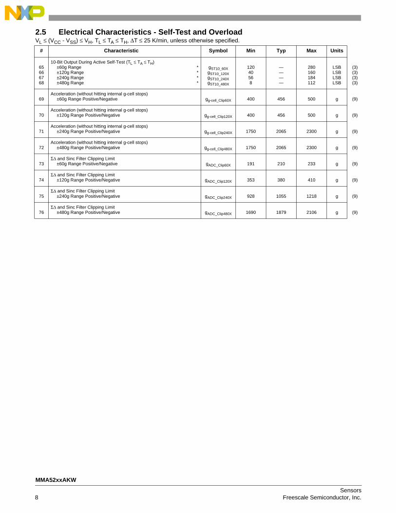
2.5 Electrical Characteristics - Self-Test and OverloadVL ≤ (VCC - VSS) ≤ VH, TL ≤ TA ≤ TH, ΔT ≤ 25 K/min, unless otherwise specified.
# Characteristic Symbol Min Typ Max Units
65666768
10-Bit Output During Active Self-Test (TL ≤ TA ≤ TH)±60g Range±120g Range±240g Range±480g Range
****
gST10_60XgST10_120XgST10_240XgST10_480X
12040568
————
280160184112
LSBLSBLSBLSB
(3)(3)(3)(3)
69Acceleration (without hitting internal g-cell stops)
±60g Range Positive/Negative gg-cell_Clip60X 400 456 500 g (9)
70Acceleration (without hitting internal g-cell stops)
±120g Range Positive/Negative gg-cell_Clip120X 400 456 500 g (9)
71Acceleration (without hitting internal g-cell stops)
±240g Range Positive/Negative gg-cell_Clip240X 1750 2065 2300 g (9)
72Acceleration (without hitting internal g-cell stops)
±480g Range Positive/Negative gg-cell_Clip480X 1750 2065 2300 g (9)
73ΣΔ and Sinc Filter Clipping Limit
±60g Range Positive/Negative gADC_Clip60X 191 210 233 g (9)
74ΣΔ and Sinc Filter Clipping Limit
±120g Range Positive/Negative gADC_Clip120X 353 380 410 g (9)
75ΣΔ and Sinc Filter Clipping Limit
±240g Range Positive/Negative gADC_Clip240X 928 1055 1218 g (9)
76ΣΔ and Sinc Filter Clipping Limit
±480g Range Positive/Negative gADC_Clip480X 1690 1879 2106 g (9)
Sensors8 Freescale Semiconductor, Inc.
MMA52xxAKW

2.6 Dynamic Electrical Characteristics - PSI5VL ≤ (VCC - VSS) ≤ VH, TL ≤ TA ≤ TH, ΔT ≤ 25 K/min, unless otherwise specified
2.7 Dynamic Electrical Characteristics - Signal ChainVL ≤ (VCC - VSS) ≤ VH, TL ≤ TA ≤ TH, ΔT ≤ 25 K/min, unless otherwise specified
# Characteristic Symbol Min Typ Max Units
77787980818283848586
Initialization TimingPhase 1Phase 2 (10-Bit, Asynchronous Mode 0, k = 8)Phase 3 (10-Bit, Asynchronous Mode 0, ST_RPT = 0)Offset Cancellation Stage 1 Operating TimeOffset Cancellation Stage 2 Operating TimeSelf-Test Stage 1 Operating TimeSelf-Test Stage 2 Operating TimeSelf-Test Stage 3 Operating TimeSelf-Test RepetitionsProgramming Mode Entry Window
tPSI5_INIT1tPSI5_INIT2_10a0tPSI5_INIT3_10a0
tOC1tOC2tST1tST2tST3
ST_RPTtPME
————————0—
532000 / fOSC512 * tASYNC19 * tASYNC
320000 / fOSC280000 / fOSC128000 / fOSC128000 / fOSC128000 / fOSC
—300000 / fOSC
————————5—
ssssssss
s
(7)(7)
(7, 12)(7)(7)(7)(7)(7)
(7, 12)(7)
87 Data Transmission Single Bit Time (PSI5 Low Bit Rate) * tBIT_LOW 7.6000 8.0000 8.4000 μs (7)
88Modulation Current (20% to 80% of IMOD - IIDLE)
Rise Time tRISE 324 463 602 ns (3)
89 Position of bit transition (PSI5 Low Baud Rate) * tBittrans_LowBaud 49 50 51 % (7)
90 Asynchronous Response Time * tASYNC — 912 / fOSC — s (7)
# Characteristic Symbol Min Typ Max Units
91 Internal Oscillator Frequency * fOSC 3.80 4 4.20 MHz (1)
9293
DSP Low-Pass Filter (Note15)Cutoff frequency LPF0 (referenced to 0 Hz)Filter Order LPF0
**
fC_LPF0OLPF0
⎯⎯
4003
⎯⎯
Hz1
(7)(7)
949596979899100101102103104105
DSP Offset Cancellation Low-Pass Filter (Note 15)Offset Cancellation Low-Pass Filter Input Sample RateStage 1 Cutoff frequency, Startup Phase 1Stage 1 Filter Order, Startup Phase 1Stage 2 Cutoff frequency, Startup Phase 1Stage 2 Filter Order, Startup Phase 1Cutoff frequency, Option 0Filter Order, Option 0Offset Cancellation Output Update Rate (10-Bit Mode)Offset Cancellation Output Step Size (10-Bit Mode)Offset Monitor Update FrequencyOffset Monitor Count LimitOffset Monitor Counter Size
tOC_SampleRatefC_OC10OOC10fC_OC03OOC03fC_OC0OOC0
tOffRate_10OFFStep_10
OFFMONOSCOFFMONCNTLIMITOFFMONCNTSIZE
⎯⎯⎯⎯⎯⎯⎯⎯⎯⎯⎯⎯
25610.0
10.300
10.100
1fOSC / 2e6
0.5fOSC/2000
40968192
⎯⎯⎯⎯⎯⎯⎯⎯⎯⎯⎯⎯
μsHz1
Hz1
Hz1s
LSBHz11
(7)(7)(7)(7)(7)(7)(7)(7)(7)(7)(7)(7)
106107108109
Sensing Element Natural Frequency ±60g±120g±240g±480g
fgcell_X60fgcell_X120fgcell_X240fgcell_X480
12651126512600026000
⎯⎯⎯⎯
13871138712870028700
HzHzHzHz
(9)(9)(9)(9)
110111112113
Sensing Element Rolloff Frequency (-3 db)±60g±120g±240g±480g
fgcell_X60fgcell_X120fgcell_X240fgcell_X480
938938
39523952
⎯⎯⎯⎯
25922592
1437014370
HzHzHzHz
(9)(9)(9)(9)
114115116117
Sensing Element Damping Ratio±60g±120g±240g±480g
ζgcell_X60ζgcell_X120ζgcell_X240ζgcell_X480
2.7602.7601.2601.260
⎯⎯⎯⎯
6.7706.7703.6023.602
⎯⎯⎯⎯
(9)(9)(9)(9)
118119120121
Sensing Element Delay (@100 Hz)±60g±120g±240g±480g
fgcell_delay_X60fgcell_delay_X120fgcell_delay_X240fgcell_delay_X480
63631313
⎯⎯⎯⎯
1701704040
μsμsμsμs
(9)(9)(9)(9)
122 Package Resonance Frequency fPackage 100 ⎯ ⎯ kHz (9)
SensorsFreescale Semiconductor, Inc. 9
MMA52xxAKW

2.8 Dynamic Electrical Characteristics - Supply and SPIVL ≤ (VCC - VSS) ≤ VH, TL ≤ TA ≤ TH, ΔT ≤ 25 K/min, unless otherwise specified
1. Parameters tested 100% at final test.2. Parameters tested 100% at wafer probe.3. Verified by characterization4. * Indicates critical characteristic.5. Verified by qualification testing.6. Parameters verified by pass/fail testing in production.7. Functionality guaranteed by modeling, simulation and/or design verification. Circuit integrity assured through IDDQ and scan testing. Timing
is determined by internal system clock frequency.8. N/A.9. Verified by simulation.10. N/A.11. Measured at VCC pin; VSYNC guaranteed across full VIDLE range.12. Self-Test repeats on failure up to a ST_RPTMAX times before transmitting Sensor Error Message.13. N/A.14. Thermal resistance between the die junction and the exposed pad; cold plate is attached to the exposed pad.15. Filter cutoff frequencies are directly dependent upon the internal oscillator frequency.
# Characteristic Symbol Min Typ Max Units
123 Quiescent Current Settling Time (Power Applied to Iq = IIDLE ± 2mA) tSET ⎯ ⎯ 5 ms (3)
124 Reset Recovery Internal Delay (After internal POR) tINT_INIT ⎯ 16000 / fOSC ⎯ s (7)
125126127
VCC Micro-cut (CBUF=CREG=CREGA=1 μF)Survival Time (VCC disconnect without Reset, CBUF=CREG=CREGA=700 nF)Survival Time (VCC disconnect without Reset, CBUF=CREG=CREGA=1 μF)Reset Time (VCC disconnect above which Reset is guaranteed)
tVCC_MICROCUTmintVCC_MICROCUT
tVCC_RESET
3050⎯
⎯⎯⎯
⎯⎯
1000
μsμsμs
(3)(3)(3)
128129
VBUF, Capacitor Monitor Disconnect Time (Figure 9)POR to first Capacitor Test DisconnectDisconnect Delay, Asynchronous Mode (Figure 9)
tPOR_CAPTESTtCAPTEST_ADLY
⎯⎯
12000 / fOSC688 / fOSC
⎯⎯
ss
(7)(7)
130131
VREG, VREGA Capacitor MonitorPOR to first Capacitor Test DisconnectDisconnect Rate
tPOR_CAPTESTtCAPTEST_RATE
⎯⎯
12000 / fOSC256 / fOSC
⎯⎯
ss
(7)(7)
132133134135136137138139140141142143144145
Serial Interface Timing (See Figure 6, CDOUT ≤ 80 pF, RDOUT ≥ 10 kΩ)Clock (SCLK) period (10% of VCC to 10% of VCC)Clock (SCLK) high time (90% of VCC to 90% of VCC)Clock (SCLK) low time (10% of VCC to 10% of VCC)Clock (SCLK) rise time (10% of VCC to 90% of VCC)Clock (SCLK) fall time (90% of VCC to 10% of VCC)CS asserted to SCLK high (CS = 10% of VCC to SCLK = 10% of VCC)CS asserted to DOUT valid (CS = 10% of VCC to DOUT = 10/90% of VCC)Data setup time (DIN = 10/90% of VCC to SCLK = 10% of VCC)DIN Data hold time (SCLK = 90% of VCC to DIN = 10/90% of VCC)DOUT Data hold time (SCLK = 90% of VCC to DOUT = 10/90% of VCC)SCLK low to data valid (SCLK = 10% of VCC to DOUT = 10/90% of VCC)SCLK low to CS high (SCLK = 10% of VCC to CS = 90% of VCC)CS high to DOUT disable (CS = 90% of VCC to DOUT = Hi Z)CS high to CS low (CS = 90% of VCC to CS = 90% of VCC)
tSCLKtSCLKHtSCLKLtSCLKRtSCLKFtLEAD
tACCESStSETUP
tHOLD_INtHOLD_OUT
tVALIDtLAG
tDISABLEtCSN
320120120⎯⎯60⎯20100⎯60⎯
1000
⎯⎯⎯1515⎯⎯⎯⎯⎯⎯⎯⎯⎯
⎯⎯⎯4028⎯60⎯⎯⎯50⎯60⎯
nsnsnsnsnsnsnsnsnsnsnsnsnsns
(9)(9)(9)(9)(9)(9)(9)(9)(9)(9)(9)(9)(9)(9)
Sensors10 Freescale Semiconductor, Inc.
MMA52xxAKW

Figure 5. Powerup Timing
Figure 6. Serial Interface Timing
VCC
POR
VCC_UV_f + VCC_HYST
Time
VREG
VBUF
VCC_UV_f
VBUF_UV_f + VBUF_HYST
VBUF_UV_f
VREG_UV_f + VREG_HYST
VREG_UV_f
VREG
VREGA_UV_f+VREGA_HYST
VREGA_UV_f
Response Terminated if in process
tSCLK
SCLK
DIN
CS
DOUT
tSCLKH
tSCLKLtACCESS
tSCLKR tSCLKFtLEADtCSN
tSETUP
tHOLD_IN
tVALID tDISABLEtHOLD_OUT
tLAG
SensorsFreescale Semiconductor, Inc. 11
MMA52xxAKW

3 Functional Description3.1 User Accessible Data Array
A user accessible data array allows for each device to be customized. The array consists of an OTP factory programmable block, an OTP user programmable block, and read-only registers for device status. The OTP blocks incorporate independent error detection circuitry for fault detection (reference Section 3.2). Portions of the factory programmable array are reserved for factory-programmed trim values. The user accessible data is shown in Table 2.
Type codes R: Readable register via PSI5
3.1.1 Device Serial Number RegistersA unique serial number is programmed into the serial number registers of each device during manufacturing. The serial num-
ber is composed of the following information:
Serial numbers begin at 1 for all produced devices in each lot and are sequentially assigned. Lot numbers begin at 1 and are sequentially assigned. No lot will contain more devices than can be uniquely identified by the 13-bit serial number. Depending on lot size and quantities, all possible lot numbers and serial numbers may not be assigned.
The serial number registers are included in the factory programmed OTP CRC verification. Reference Section 3.2 for details regarding the CRC verification. Beyond this, the contents of the serial number registers have no impact on device operation or performance, and are only used for traceability purposes.
Table 2. User Accessible Data
Byte Addr
(XLong Msg)
RegisterNibble Addr(Long Msg)
Bit Function Nibble Addr(Long Msg)
Bit FunctionType
7 6 5 4 3 2 1 0
$00 SN0 $01 SN[7] SN[6] SN[5] SN[4] $00 SN[3] SN[2] SN[1] SN[0]
R
$01 SN1 $03 SN[15] SN[14] SN[13] SN[12] $02 SN[11] SN[10] SN[9] SN[8]
$02 SN2 $05 SN[23] SN[22] SN[21] SN[20] $04 SN[19] SN[18] SN[17] SN[16]
$03 SN3 $07 SN[31] SN[30] SN[29] SN[28] $06 SN[27] SN[26] SN[25] SN[24]
$04 DEVCFG1 $09 0 0 1 0 $08 0 RNG[2] RNG[1] RNG[0]
$05 DEVCFG2 $0B 0 0 0 0 $0A 0 0 0 0
$06 DEVCFG3 $0D 0 0 0 0 $0C 0 0 0 0
$07 DEVCFG4 $0F 0 0 0 0 $0E 0 0 0 0
$08 DEVCFG5 $11 0 0 0 0 $10 0 0 0 0
$09 DEVCFG6 $13 0 1 0 0 $12 0 0 0 0
$0A DEVCFG7 $15 0 0 0 0 $14 0 0 0 0
$0B DEVCFG8 $17 1 0 1 0 $16 0 0 0 0
$0C SC $19 0 TM_B RESERVED IDEN_B $18 OC_INIT_B IDEF_B OFF_B 0
$0D MFG_ID $1B 0 0 0 0 $1A 0 0 0 0
Bit Range Content
SN[12:0] Serial Number
SN[31:13] Lot Number
Sensors12 Freescale Semiconductor, Inc.
MMA52xxAKW

3.1.2 Factory Configuration Register (DEVCFG1)The factory configuration register is a factory programmed, read-only register which contains user specific device configuration
information. The factory configuration register is included in the factory programmed OTP CRC verification.
3.1.2.1 Range Indication Bits (RNG[2:0])The range indication bits are factory programmed and indicate the full-scale range of the device as shown below.
3.1.3 Status Check Register (SC)The status check register is a read-only register containing device status information.
3.1.3.1 Test Mode Flag (TM_B)The test mode bit is cleared if the device is in test mode.
3.1.3.2 Internal Data Error Flag (IDEN_B)The internal data error bit is cleared if a register data error detection mismatch is detected in the user accessible OTP array.
A device reset is required to clear the error.
Location Bit
Address Register 7 6 5 4 3 2 1 0
$04 DEVCFG1 0 0 1 0 0 RNG[2] RNG[1] RNG[0]
Factory Default 0 0 1 0 0 0 0 0
RNG[2] RNG[1] RNG[0] Full-Scale Acceleration Range g-Cell Design
PSI5 Init DataTransmission (D9)Reference Table 9
0 0 0 Reserved N/A 0001
0 0 1 ±60g Medium-g 0111
0 1 0 Reserved N/A 0010
0 1 1 ±120 g Medium-g 1000
1 0 0 Reserved N/A 0011
1 0 1 ±240 g High-g 1001
1 1 0 Reserved N/A 0100
1 1 1 ±480 g High-g 1010
Location Bit
Address Register 7 6 5 4 3 2 1 0
$0C SC 0 TM_B RESERVED IDEN_B OC_INIT_B IDEF_B OFF_B 0
TM_B Operating Mode
0 Test Mode is active
1 Test Mode is not active
IDEN_B Error Condition
0 Error detection mismatch in user programmable OTP array
1 No error detected
SensorsFreescale Semiconductor, Inc. 13
MMA52xxAKW

3.1.3.3 Offset Cancellation Init Status Flag (OC_INIT_B)The offset cancellation initialization status bit is set once the offset cancellation initialization process is complete, and the filter
has switched to normal mode.
3.1.3.4 Internal Factory Data Error Flag (IDEF_B)The internal factory data error bit is cleared if a register data CRC fault is detected in the factory programmable OTP array. A
device reset is required to clear the error.
3.1.3.5 Offset Error Flag (OFF_B)The offset error flag is cleared if the acceleration signal reaches the offset limit.
3.2 OTP Array Error DetectionThe Factory programmed OTP array is verified for errors with a 3-bit CRC. The CRC verification is enabled only when the
factory programmed array is locked. The CRC verification uses a generator polynomial of g(x) = X3 + X + 1, with a seed value = ‘111’.
The CRC is continuously calculated on the factory programmable array with the exception of the factory lock bits. Bits are fed in from right to left (LSB first), and top to bottom (lower addresses first) in the register map. The calculated CRC is then compared against the stored 3 bit CRC. If a CRC error is detected in the OTP array, the IDEF_B bit is cleared in the SC register.
The CRC verification is completed on the memory registers which hold a copy of the fuse array values, not the fuse array val-ues.
OC_INIT_B Error Condition
0 Offset Cancellation in initialization
1 Offset Cancellation initialization complete (tOC1 and tOC2 expired)
IDEF_B Error Condition
0 CRC error in factory programmable OTP array
1 No error detected
OFF_B Error Condition
0 Offset error detected
1 No error detected
Sensors14 Freescale Semiconductor, Inc.
MMA52xxAKW

3.3 Voltage RegulatorsThe device derives its internal supply voltage from the VCC and VSS pins. Separate internal voltage regulators are used for the
analog (VREGA) and digital circuitry (VREG). The analog and digital regulators are supplied by a buffer regulator (VBUF) to provide immunity from EMC and supply dropouts on VCC. External filter capacitors are required, as shown in Figure 1.
The voltage regulator module includes voltage monitoring circuitry which holds the device in reset following power-on until the internal voltages have increased above the undervoltage detection thresholds. The voltage monitor asserts internal reset when the external supply or internally regulated voltages fall below the undervoltage detection thresholds. A reference generator pro-vides a reference voltage for the ΣΔ converter.
Figure 7. Voltage Regulation and Monitoring
VREGA
VREG
VCC
VOLTAGEREGULATOR
REFERENCEGENERATOR
VREGA = 2.50 V
DIGITALLOGIC
DSP
OTPARRAY
OSCILLATOR
ΣΔCONVERTER
BIASGENERATOR
TRIMTRIM
VREF
VREF_MOD = 1.250 V
VREG = 2.50 V
VOLTAGEREGULATOR
VBUF
BANDGAPREFERENCE
VBUF
VBUF
VREF
VREGA
VREF
POR
VCC COMPARATOR
VREF
COMPARATOR
COMPARATOR
VBUF
COMPARATORVREGA
VREG
VOLTAGEREGULATOR
Micro-cut
TRIM
TRIM
SensorsFreescale Semiconductor, Inc. 15
MMA52xxAKW

3.3.1 VBUF, VREG, and VREGA Regulator CapacitorThe internal regulators require an external capacitor between each of the regulator pins (VBUF, VREG, or VREGA) and the as-
sociated the VSS / VSSA pin for stability. Figure 1 shows the recommended types and values for each of these capacitors.
3.3.2 VCC, VBUF, VREG, and VREGA Undervoltage MonitorA circuit is incorporated to monitor the supply voltage (VCC) and all internally regulated voltages (VBUF, VREG, and VREGA). If
any of internal regulator voltages fall below the specified undervoltage thresholds in Section 2, the device will be reset. If VCC falls below the specified threshold, PSI5 transmissions are terminated for the present response. Once the supply returns above the threshold, the device will respond to the next detected sync pulse. Reference Figure 8.
Figure 8. VCC Micro-Cut Response
VCC
POR
VREG
Time
VBUF
VREGA
VCC undervoltage detected
Response Terminated
IDATA
VCC micro-cut occurs
Sensors16 Freescale Semiconductor, Inc.
MMA52xxAKW
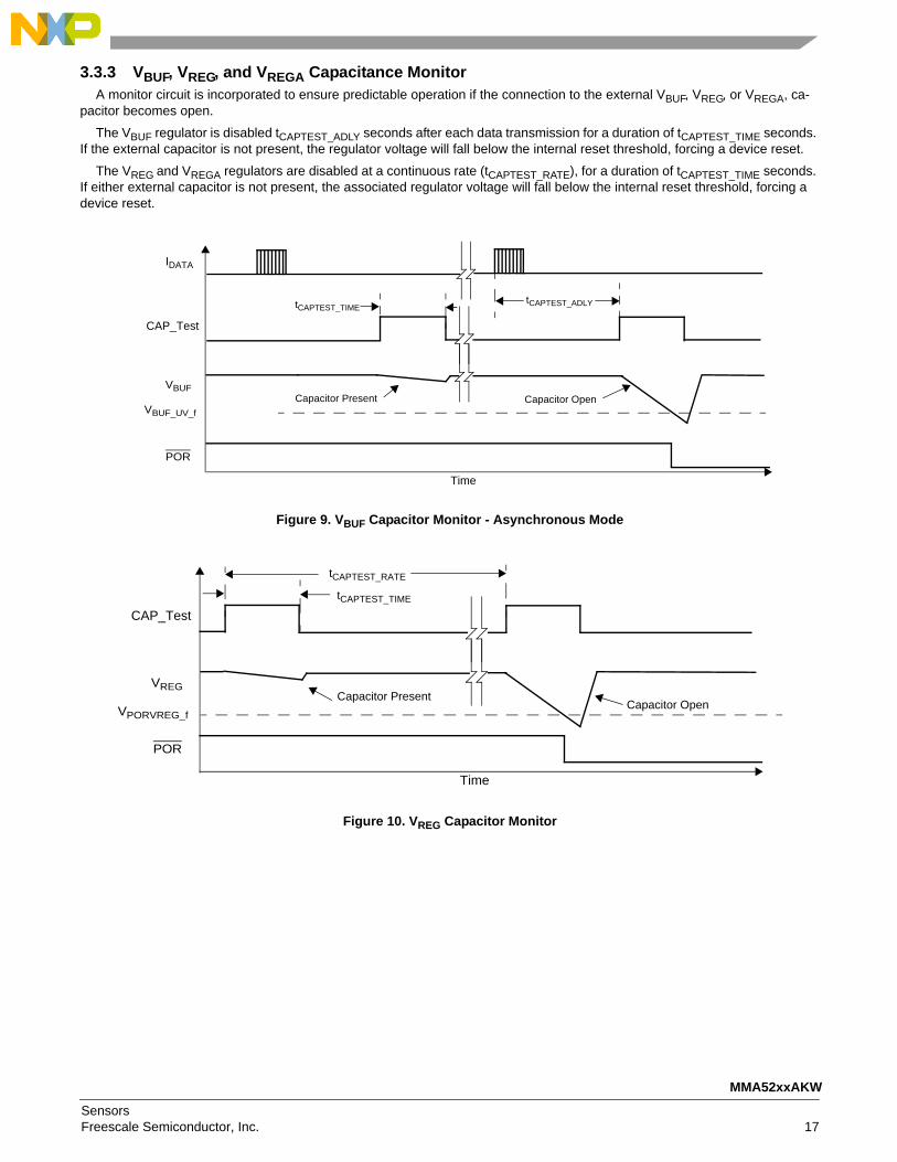
3.3.3 VBUF, VREG, and VREGA Capacitance MonitorA monitor circuit is incorporated to ensure predictable operation if the connection to the external VBUF, VREG, or VREGA, ca-
pacitor becomes open.
The VBUF regulator is disabled tCAPTEST_ADLY seconds after each data transmission for a duration of tCAPTEST_TIME seconds. If the external capacitor is not present, the regulator voltage will fall below the internal reset threshold, forcing a device reset.
The VREG and VREGA regulators are disabled at a continuous rate (tCAPTEST_RATE), for a duration of tCAPTEST_TIME seconds. If either external capacitor is not present, the associated regulator voltage will fall below the internal reset threshold, forcing a device reset.
Figure 9. VBUF Capacitor Monitor - Asynchronous Mode
Figure 10. VREG Capacitor Monitor
CAP_Test
VBUF
Time
Capacitor PresentVBUF_UV_f
POR
Capacitor Open
tCAPTEST_TIME
IDATA
tCAPTEST_ADLY
CAP_Test
VREG
Time
Capacitor Present
POR
Capacitor Open
tCAPTEST_TIME
tCAPTEST_RATE
VPORVREG_f
SensorsFreescale Semiconductor, Inc. 17
MMA52xxAKW

Figure 11. VREGA Capacitor Monitor
3.4 Internal OscillatorA factory trimmed oscillator is included as specified in Section 2.
3.5 Acceleration Signal Path3.5.1 Transducer
The transducer is an overdamped mass-spring-damper system defined by the following transfer function:
where:
ζ = Damping Ratio
ωn = Natural Frequency = 2 ∗ Π ∗ fnReference Section 2.7 for transducer parameters.
3.5.2 ΣΔ ConverterA sigma delta modulator converts the differential capacitance of the transducer to a 1 MHz data stream that is input to the DSP
block.
Figure 12. ΣΔ Converter Block Diagram
CAP_Test
VREGA
Time
Capacitor PresentVPORREGA_f
POR
Capacitor Open
tCAPTEST_TIME
tCAPTEST_RATE
H s( )ωn
2
s2 2 ξ ωn s⋅ ⋅ ⋅ ωn2+ +
---------------------------------------------------------=
1-BITQUANTIZER
z-1
1 - z-1
z-1
1 - z-1
FIRSTINTEGRATOR
SECONDINTEGRATOR
α1=
β1
α2
β2
VX
CINT1
g-CELL
CBOT
CTOP
ΔC = CTOP - CBOT
ΣΔ_OUT
V = ±2 × VREF
ADC
DACV = ΔC x VX / CINT1
Sensors18 Freescale Semiconductor, Inc.
MMA52xxAKW

3.5.3 Digital Signal Processing BlockA Digital Signal Processing (DSP) block is used to perform signal filtering and compensation. A diagram illustrating the signal
processing flow within the DSP block is shown in Figure 13.
Figure 13. Signal Chain Diagram
3.5.3.1 Decimation Sinc FilterThe serial data stream produced by the ΣΔ converter is decimated and converted to parallel values by a 3rd order 16:1 sinc
filter with a decimation factor of 16.
Table 3. Signal Chain Characteristics
DescriptionSample
Time(μs)
DataWidth(Bits)
Over Range(Bits
SignalWidth(Bits)
SignalNoise(Bits)
SignalMargin(Bits)
Typical Block Latency Reference
A SD 1 1 1203/fosc
Section 3.5.2
B SINC Filter 16 20 13 Section 3.5.3.2
C Low-Pass Filter 16 26 4 10 3 9 Reference Section 3.5.3.2 Section 3.5.3.2
D Compensation 16 26 4 10 3 968/fosc
E Down Sampling 16 26 4 10 3 9
F High-Pass Filter 16 26 4 10 3 9 Reference Section 3.5.3.3 Section 3.5.3.3
GDSP Sampling
16 10 4/fosc Section 3.5.3.510-Bit Output Scaling
H Interpolation 1 10 64/fosc Section 3.5.3.5
ΣΔ_OUT SINC FILTER LOW-PASS FILTER
OUTPUTOUTPUT
COMPENSATIONA B C D
INTERPOLATIONSCALINGFOFFSET
RATE LIMITING
OFFSET CANCELLATIONDOWNSAMPLING LOW-PASS FILTERE CANCELLATION
OUTPUTG H
H z( ) 1 z 16––16 1 z 1––( )×-------------------------------------
3=
SensorsFreescale Semiconductor, Inc. 19
MMA52xxAKW

Figure 14. Sinc Filter Response, tS = 16 μs
Sensors20 Freescale Semiconductor, Inc.
MMA52xxAKW

3.5.3.2 Low-Pass FilterData from the Sinc filter is processed by an infinite impulse response (IIR) low-pass filter.
Note: Low-Pass Filter values do not include g-cell frequency response.
H z( ) a0n11 z0⋅( ) n12 z 1–⋅( ) n13 z 2–⋅( )+ +
d11 z0⋅( ) d12 z 1–⋅( ) d13 z 2–⋅( )+ +-------------------------------------------------------------------------------------------------
n21 z0⋅( ) n22 z 1–⋅( ) n23 z 2–⋅( )+ +
d11 z0⋅( ) d22 z 1–⋅( ) d23 z 2–⋅( )+ +-------------------------------------------------------------------------------------------------⋅ ⋅=
Table 4. Low-Pass Filter Coefficients
Description Filter Coefficients Group Delay
400 Hz, 3-Pole LPF
a0 5.189235225042199e-02
2816/fosc
n11 1.629077582099646e-03 d11 1.0
n12 1.630351547919014e-03 d12 -9.481076477495780e-01
n13 0 d13 0
n21 2.500977520825902e-01 d21 1.0
n22 4.999999235890745e-01 d22 -1.915847097557409e+00
n23 2.499023243303036e-01 d23 9.191065266874253e-01
SensorsFreescale Semiconductor, Inc. 21
MMA52xxAKW

Figure 15. Low-Pass Filter Characteristics: fC = 400 Hz, 3-Pole, tS = 16 μs
Sensors22 Freescale Semiconductor, Inc.
MMA52xxAKW

3.5.3.3 Offset CancellationThe device provides an offset cancellation circuit to remove internal offset error. A block diagram of the offset cancellation is
shown in Figure 16.
Figure 16. Offset Cancellation Block DiagramThe transfer function for the offset LPF is:
Response parameters are specified in Section 2 and the offset LPF coefficients are specified in Table 6.
During startup, two phases of the offset LPF are used to allow for fast convergence of the internal offset error during initializa-tion. The timing and characteristics of each phase are shown in Table 5 and Table 6 and specified in Section 2. For more infor-mation regarding the startup timing, reference the PSI5 initialization information in Section 4.4. The offset low-pass filter used in normal operation is selected by the OC_FILT bit as shown in Table 5.
During the Initialization Self-Test phase, the offset cancellation circuit output value is frozen.
During normal operation, output rate limiting is applied to the output of the high-pass filter. Rate limiting updates the offset can-cellation output by OFFStep_xx LSB every tOffRate_xx seconds.
TO_OUTPUT SCALINGOFFSET CANCELLATION
a0n1 n2 z 1–⋅( )+
d1 d2 z 1–⋅( )+-------------------------------------⋅
LOW-PASS FILTERINPUT DATAINC/DEC
COUNTER
CLK
OUT
0.5 Hz (Derived from fOSC)
OFFMONNEG
OFFMONPOS
OFF_ERR
INC/DEC
COUNTER
CLK
OUT
UP/DOWN
2 kHz (Derived from fOSC)
OFFMONCNTLIMIT
Input Data downsampled to 256μs
H z( ) ao0no1 no2 z 1–⋅( )+
do1 do2 z 1–⋅( )+----------------------------------------------⋅=
Table 5. Offset Cancellation Startup Characteristics and Timing
Offset CancellationStartup Phase Offset LPF Output Rate Limiting Total Time for Phase
1 10 Hz Bypassed 80 ms
2 0.3 Hz Bypassed 70 ms
Self-Test 0.3 Hz Bypassed (Frozen during ST2) 96 ms per Self-Test Sequence (up to 6 repeats)
Complete 0.1 Hz Enabled N/A
SensorsFreescale Semiconductor, Inc. 23
MMA52xxAKW

Figure 17. 10 Hz Offset Cancellation Low-Pass Filter Characteristics
Figure 18. 0.1 Hz Offset Cancellation Low-Pass Filter Characteristics
Table 6. High-Pass Filter CoefficientsDescription Coefficients Group Delay
10 Hz HPF
ao0 0.015956938266754
16.384 msno1 0.499998132328277 do1 1.0
no2 0.499998132328277 do2 -0.984043061733246
0.3 Hz HPF
ao0 0.000482380390167
537.6 msno1 0.499938218213271 do1 1.0
no2 0.499938218213271 do2 -0.999517619609833
0.1 Hz HPF
ao0 0.0001608133316040
1591msno1 0.4999999403953552 do1 1.0
no2 0.4999999403953552 do2 -0.9998391270637512
Sensors24 Freescale Semiconductor, Inc.
MMA52xxAKW

3.5.3.4 Offset MonitorThe device includes an offset monitor circuit. The output of the single pole low-pass filter in the offset cancellation block is
continuously monitored against the offset limits specified in Section 2.4. An up/down counter is employed to count up If the output exceeds the limits, and to count down if the output is within the limits. The output of the counter is compared against the count limit OFFMONCNTLIMIT. If the counter exceeds the limit, the OFF_B flag in the SC register is cleared. The counter rails once the max counter value is reached (OFFMONCNTSIZE). The offset monitor is disabled during Initialization Phase 1, Phase 2, and Phase 3.
3.5.3.5 Data InterpolationThe device includes 16 to 1 linear data interpolation to minimize the system sample jitter. Each result produced by the digital
signal processing chain is delayed one sample time.
3.5.3.6 Output ScalingThe 26-bit digital output from the DSP is clipped and scaled to a 10-bit word which spans the acceleration range of the device.
Figure 19 shows the method used to establish the output acceleration data word from the 26-bit DSP output.
Figure 19. 10-Bit Output Scaling Diagram
Over Range Signal Noise Margin
D25 D24 D23 D22 D21 D20 D19 D18 D17 D16 D15 D14 D13 D12 D11 D10 D9 D8 ... D2 D1 D0
10-bit Data Word D21 D20 D19 D18 D17 D16 D15 D14 D13 D12 Using Rounding
SensorsFreescale Semiconductor, Inc. 25
MMA52xxAKW
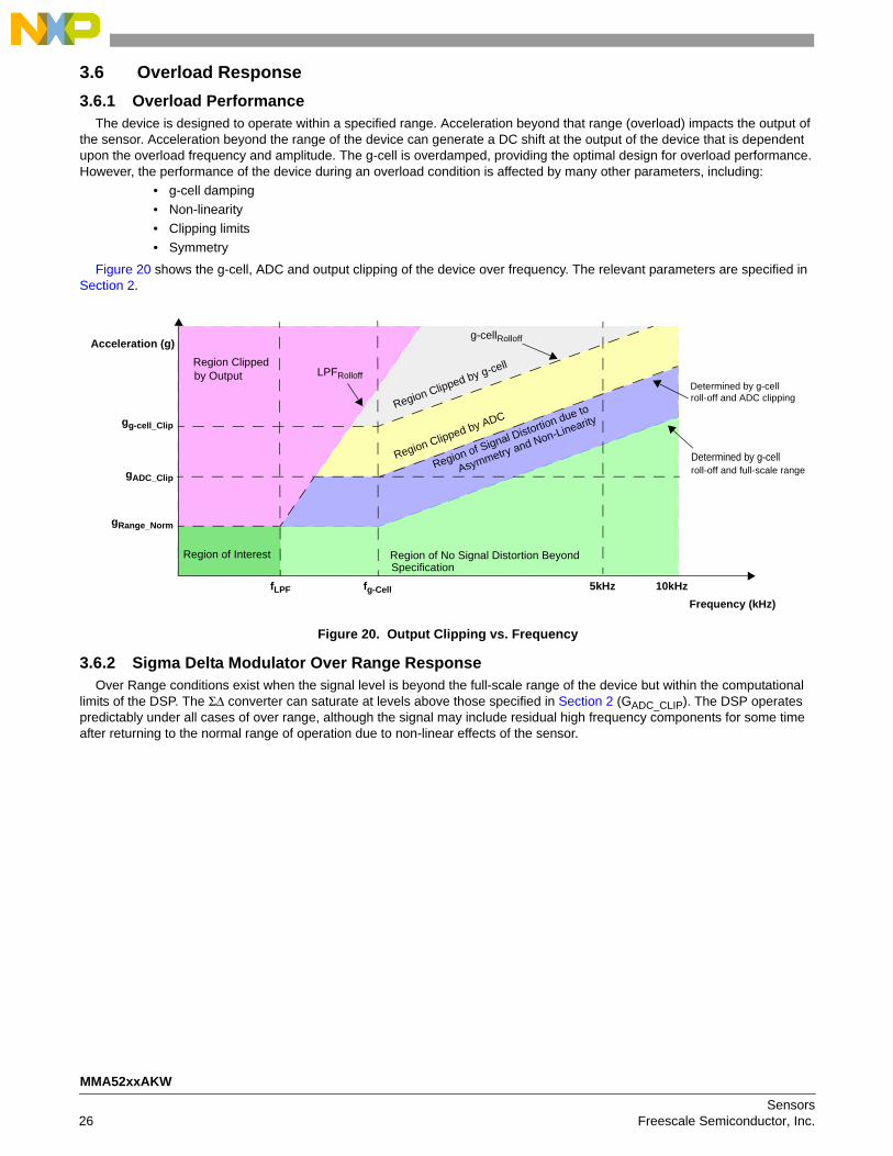
3.6 Overload Response3.6.1 Overload Performance
The device is designed to operate within a specified range. Acceleration beyond that range (overload) impacts the output of the sensor. Acceleration beyond the range of the device can generate a DC shift at the output of the device that is dependent upon the overload frequency and amplitude. The g-cell is overdamped, providing the optimal design for overload performance. However, the performance of the device during an overload condition is affected by many other parameters, including:
• g-cell damping• Non-linearity• Clipping limits• Symmetry
Figure 20 shows the g-cell, ADC and output clipping of the device over frequency. The relevant parameters are specified in Section 2.
Figure 20. Output Clipping vs. Frequency
3.6.2 Sigma Delta Modulator Over Range ResponseOver Range conditions exist when the signal level is beyond the full-scale range of the device but within the computational
limits of the DSP. The ΣΔ converter can saturate at levels above those specified in Section 2 (GADC_CLIP). The DSP operates predictably under all cases of over range, although the signal may include residual high frequency components for some time after returning to the normal range of operation due to non-linear effects of the sensor.
5kHz fg-Cell fLPF
gADC_Clip
gg-cell_Clip
Determined by g-cell
10kHz
g-cellRolloffAcceleration (g)
Frequency (kHz)
LPFRolloff
Region Clipped by g-cell
Region Clipped by ADC
Region of Signal Distortion due to
Asymmetry and Non-Linearity
Region of No Signal Distortion BeyondSpecification
Region of Interest
roll-off and ADC clipping
gRange_Norm
Determined by g-cell roll-off and full-scale range
Region Clippedby Output
Sensors26 Freescale Semiconductor, Inc.
MMA52xxAKW

4 PSI5 Layer and Protocol4.1 Communication Interface Overview
The communication interface between a master device and the MMA52xx is established via a PSI5 compatible 2-wire inter-face. Figure 21 shows the PSI5 master to slave connections.
Figure 21. PSI5 Satellite Interface Diagram
4.2 Data Transmission Physical LayerThe device uses a two wire interface for both its power supply (VCC), and data transmission. Data transmissions from the de-
vice to the PSI5 master are accomplished via modulation of the current on the power supply line.
4.3 Data Transmission Data Link Layer4.3.1 Bit Encoding
The device outputs data by modulation of the VCC current using Manchester 2 Encoding. Data is stored in a transition occurring in the middle of the bit time. The signal idles at the normal quiescent supply current. A logic low is defined as an increase in current at the middle of a bit time. A logic high is defined as a decrease in current at the middle of a bit time. There is always a transition in the middle of the bit time. If consecutive “1” or “0” data are transmitted, There will also be a transition at the start of a bit time.
Figure 22. Manchester 2 Data Bit Encoding
MMA51xxVCC
IData
SATELLITE MODULE #1
VCC
VSS
MASTER DEVICE
DiscreteComponents
VSS
IMOD CURRENT ‘0’ BIT
CONSECUTIVE‘0’ DATA BITS
IDLE CURRENT
‘1’ BITSENSED HIGH
tBITSENSED LOW
CONSECUTIVE‘1’ DATA BITS
SensorsFreescale Semiconductor, Inc. 27
MMA52xxAKW
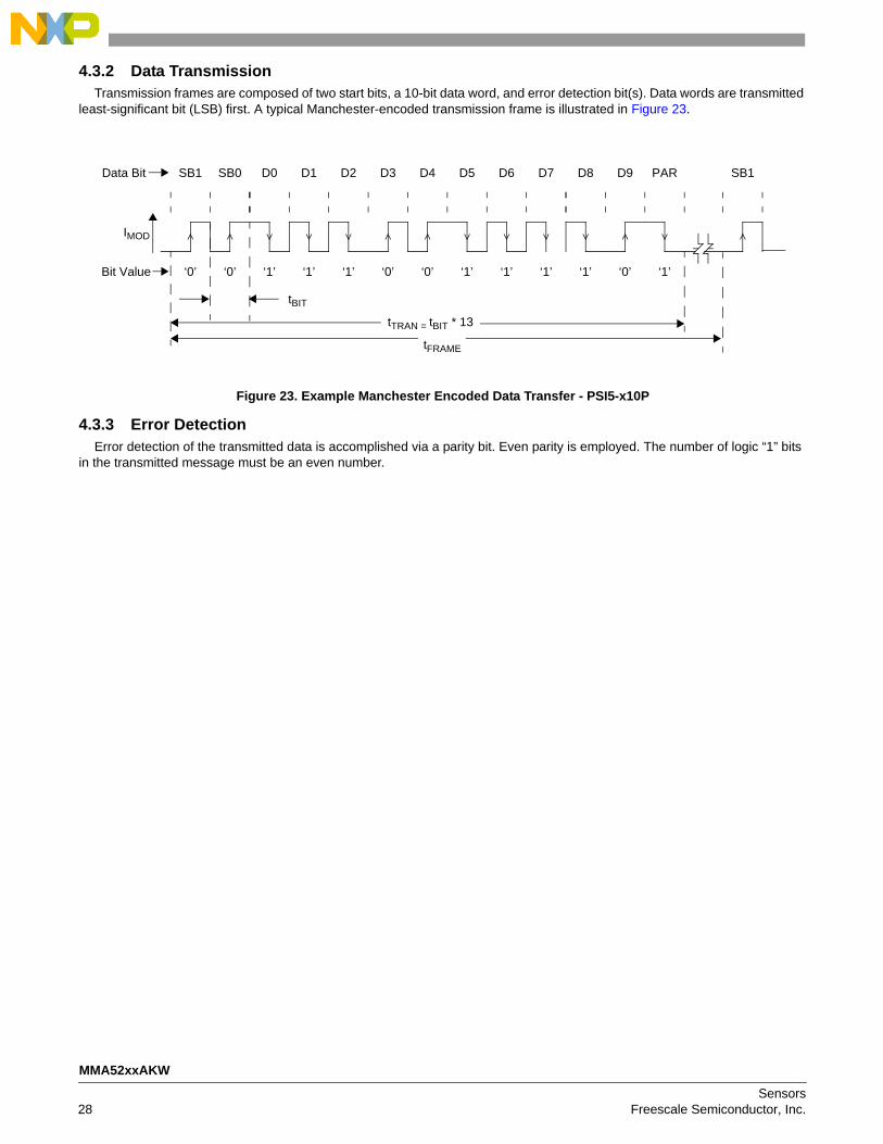
4.3.2 Data TransmissionTransmission frames are composed of two start bits, a 10-bit data word, and error detection bit(s). Data words are transmitted
least-significant bit (LSB) first. A typical Manchester-encoded transmission frame is illustrated in Figure 23.
Figure 23. Example Manchester Encoded Data Transfer - PSI5-x10P
4.3.3 Error DetectionError detection of the transmitted data is accomplished via a parity bit. Even parity is employed. The number of logic “1” bits
in the transmitted message must be an even number.
SB1 SB0 D0 D1 D2 D3 D4 D5 D8 D9 PAR
‘0’ ‘0’ ‘1’ ‘1’ ‘1’ ‘0’ ‘0’ ‘1’ ‘1’ ‘0’ ‘1’
Data Bit
Bit Value
D6 D7
‘1’ ‘1’
tFRAME
tBIT
tTRAN = tBIT * 13
IMOD
SB1
Sensors28 Freescale Semiconductor, Inc.
MMA52xxAKW

4.3.4 Data Range ValuesTable 8 shows the details for each data range.
Table 7. PSI5 Data Values
10-Bit Data ValueDescription
Decimal Hex+511 $1FF
Reserved
•••
•••
+502 $1F6+501 $1F5+500 $1F4 Sensor Defect Error Message+499 $1F3
Reserved•••
•••
+489 $1E9+488 $1E8 Sensor Busy+487 $1E7 Sensor Ready+486 $1E6 Sensor Ready, but Unlocked+485 $1E5
Reserved•••
•••
+481 $1E1+480 $1E0 Maximum positive acceleration value
•••
•••
Positive acceleration values+3 $03+2 $02+1 $010 0 0g level-1 $3FF
Negative acceleration values-2 $3FE-3 $3FD•••
•••
-480 $220 Maximum negative acceleration value-481 $21F
Initialization Data Codes10-Bit Status Data Nibble 1 - 16 (0000 - 1111) (Dx)
••
••
-496 $210-497 $20F
Initialization Data IDsBlock ID 1 - 16 (10-bit Mode) (IDx)
••
••
-512 $200
SensorsFreescale Semiconductor, Inc. 29
MMA52xxAKW

4.4 InitializationFollowing powerup, the device proceeds through an initialization process which is divided into 3 phases:
• Initialization Phase 1: No Data transmissions occur• Initialization Phase 2: Sensor self-test and transmission of configuration information• Initialization Phase 3: Transmission of “Sensor Busy”, and “Sensor Ready” / “Sensor Defect” message
Once initialization is completed the device begins normal mode operation, which continues as long as the supply voltage re-mains within the specified limits.
Figure 24. PSI5 Sensor 10-Bit InitializationDuring PSI5 initialization, the device completes an internal initialization process consisting of the following:
• Power-on Reset• Device Initialization• Program Mode Entry Verification• Offset Cancellation Initialization (2 Stages)• Self-Test
Figure 25 shows the timing for internal and external initialization.
Figure 25. Initialization Timing
INIT 1 INIT 3 NORMAL MODEINIT 2POR
IIDLE
IIDLE + IMOD
tINT_INIT
tPSI5_INIT1
Self-TestRaw OffsetCalculation
PSI5 InitializationPhase 1
tPSI5_INIT2 tPSI5_INIT3
PSI5 InitializationPhase 2
PSI5 InitializationPhase 3
PSI5 Normal Mode
PORInternalDelay
tOC1
Offset CancellationStage 1
tST1
Self-TestDeflectionVerification
tST2
Self-TestNormal DataCalculation
tST3 ST_RPT * tST
Self-TestRepeat
(If Necessary)tOC2
Offset CancellationStage 2
Sensors30 Freescale Semiconductor, Inc.
MMA52xxAKW

4.4.1 PSI5 Initialization Phase 1During PSI5 initialization phase 1, the device begins internal initialization and self checks, but transmits no data. Initialization
begins with the sequence below and shown in Figure 25:• Internal Delay to ensure analog circuitry has stabilized (tINT_INIT)• Offset Cancellation phase 1 Initialization (tOC1)• Offset Cancellation phase 2 Initialization (tOC2)
4.4.2 PSI5 Initialization Phase 2During PSI5 initialization phase 2, the device continues its internal self checks and transmits the PSI5 initialization phase 2
data. Initialization is transmitted using the initialization data codes and IDs specified in Table 9, and in the order shown in Figure 26.
Figure 26. PSI5 Initialization Phase 2 Data Transmission Order (10-bit Mode)
The Initialization phase 2 time is calculated with the following equation:
where:• TRANSNIBBLE = # of Transmissions per Data Nibble
2 for 10-bit Data: 1 for ID, and 1 for Data• k = the repetition rate for the data fields• Data Fields = 32 data fields for 10-bit data• tS-S = Sync Pulse Period
D1 D2 ... D32ID11 D11 ID12 D12 ... ID1k D1k ID21 D21 ID22 D22 ... ID2k D2k ... ID321 D321 ID322 D322 ... ID32k D32k
Repeat k times Repeat k times ... Repeat k times
tPHASE2 TRANSNIBBLE k× DataFields( ) tASYNC××=
SensorsFreescale Semiconductor, Inc. 31
MMA52xxAKW

4.4.2.1 PSI5 Initialization Phase 2In PSI5 initialization phase 2, 10-bit mode, the device transmits a sequence of sensor specific configuration and serial number
information. The transmission data is in conformance with the PSI5 specification, Revision 1.3, Revision 1.10. The data content and transmission format is shown in Table 8 and Table 9. Times are calculated using the equation in Section 4.4.2.
Table 8. Initialization Phase 2 Time
Operating Mode Repetition Rate (k) # of Transmissions Nominal Phase 2 TimeAsynchronous Mode (228 μs) 8 512 116.7 ms
Table 9. PSI5 Initialization Phase 2 DataPSI5 V1.2 Field ID #
PSI5 V1.2 Nibble ID #
Page Address
PSI5 Nibble Address Register Address Description Value
F1 D1
0
0000 Hard-coded Protocol Revision = V1.3 0100F2 D2, D3 0001, 0010 Hard-coded Number of Data Blocks = 32 0010 0000F3 D4, D5 0100, 0110 MFG_ID[7:0] Manufacturer ID 0100 0110F4 D6, D7 0101, 0110 Hard-coded Sensor Type = Acceleration (high-g) 0000 0001
F5
D8 0111 Factory Programmed Axis 0000
D9 1000
±60g: 0111±120g: 1000±240g: 1001±480g: 1010
Range Varies
F6D10 1001 DEVCFG2[7:4] Sensor Specific Information 0000D11 1010 DEVCFG2[3:0] Sensor Specific Information 0000
F7D12 1011 Hard-coded Product Revision FactoryD13 1100 Hard-coded Product Revision FactoryD14 1101 DEVCFG6[3:0] Product Revision 0000
F8
D15 1110
Factory Programmed
0001D16 1111 0010D17
1
0000 0000D18 0001 0000
F9
D19 0010 SN0 (High Nibble) MMA52xx Serial Number FactoryD20 0011 SN0 (Low Nibble) MMA52xx Serial Number FactoryD21 0100 SN1 (High Nibble) MMA52xx Serial Number FactoryD22 0101 SN1 (Low Nibble) MMA52xx Serial Number FactoryD23 0110 SN2 (High Nibble) MMA52xx Serial Number FactoryD24 0111 SN2 (Low Nibble) MMA52xx Serial Number FactoryD25 1000 SN3 (High Nibble) MMA52xx Serial Number FactoryD26 1001 SN3 (Low Nibble) MMA52xx Serial Number FactoryD27 1010
Factory Programmed
0000D28 1011 0000D29 1100 0000D30 1101 0000D31 1110 0000D32 1111 0000
Sensors32 Freescale Semiconductor, Inc.
MMA52xxAKW

4.4.3 Internal Self-TestDuring PSI5 Initialization Phase 2 and Phase 3, the device completes it’s internal self-test as described below and shown in
Figure 25.• Self-Test Phase 1 - Raw Offset Calculation
– The average offset is calculated for tST1 (Self-Test Disabled).• Self-Test Phase 2 - Self-Test Deflection Verification
– The offset cancellation value is frozen for tST2 + 2ms– Self-Test is enabled – After tST2/2, the acceleration output value is averaged for tST2/2 to determine the self-test value– The self-test value is compared against the limits specified in Section 2.5– Self-Test is disabled
• Self-Test Phase 3 - Self-Test Normal Data Calculation– The average offset is calculated for tST3 – If Self-Test passed, the device advances to normal mode– If Self-Test failed, the device repeats Self-Test Phases 1 through 3 up to ST_RPT times.
4.4.4 Initialization Phase 3During PSI5 initialization phase 3, the device completes it’s internal self checks, and transmits a combination of “Sensor Busy”,
“Sensor Ready”, or “Sensor Defect” messages as defined in Table 7. Self-Test is repeated on failure up to ST_RPT times to pro-vide immunity to misuse inputs during initialization. Self-Test terminates successfully after one successful self-test sequence.
Table 10 shows the nominal Initialization Phase 3 times for self-test repeats. Times are calculated using the following equation.
4.5 Error Handling4.5.1 Sensor Defect Message
The following failures will cause the device to transmit a “Sensor Defect” error message:
4.5.2 No Response ErrorThe following failures will cause the device to stop transmitting:
Table 10. Initialization Phase 3 Time
Operating Mode Self-TestRepetitions
# of Sensor BusyMessages
# of Sensor Ready or Sensor Defect Messages
Nominal Phase 3 Time (ms)
10-Bit Asynchronous Mode 0 (228 μs)
0 2
2
0.91
1 423 96.90
2 844 192.89
3 1265 288.88
4 1686 384.86
5 2107 480.85
Error Condition Error Type
Offset Error Temporary (Normal transmissions continue once offset returns within limits)
Self-Test Failure Latched until reset
IDEN_B, IDEF_B flag cleared Latched until reset
Error Condition Error Type
Undervoltage Failure (VCC) Temporary: Normal transmissions continue once voltage returns above failure limit)
tPSI5INIT3 ROUNDUPtINTINIT tOC1 tOC2 tST1 tST2 tST3+ +( ) STRPT 1+( )×+ + +( ) tPSI5INIT1 tPSI5INIT2xx+( )–
tASYNC--------------------------------------------------------------------------------------------------------------------------------------------------------------------------------------------------------------------------------------------- 2+⎝ ⎠⎛ ⎞ tASYNC×=
SensorsFreescale Semiconductor, Inc. 33
MMA52xxAKW

5 Package
5.1 Case Outline DrawingReference Freescale Case Outline Drawing # 98ASA00090D
http://www.freescale.com/files/shared/doc/package_info/98ASA00090D.pdf
5.2 Recommended FootprintReference Freescale Application Note AN3111, latest revision:
http://www.freescale.com/files/sensors/doc/app_note/AN3111.pdf
Table 11. Revision History
Revision number
Revision date
Description of changes
0 09/2012 • Initial release.
Sensors34 Freescale Semiconductor, Inc.
MMA52xxAKW
Document Number: MMA52xxAKWRev. 009/2012
Information in this document is provided solely to enable system and software
implementers to use Freescale products. There are no express or implied copyright
licenses granted hereunder to design or fabricate any integrated circuits based on the
information in this document.
Freescale reserves the right to make changes without further notice to any products
herein. Freescale makes no warranty, representation, or guarantee regarding the
suitability of its products for any particular purpose, nor does Freescale assume any
liability arising out of the application or use of any product or circuit, and specifically
disclaims any and all liability, including without limitation consequential or incidental
damages. “Typical” parameters that may be provided in Freescale data sheets and/or
specifications can and do vary in different applications, and actual performance may
vary over time. All operating parameters, including “typicals,” must be validated for each
customer application by customer’s technical experts. Freescale does not convey any
license under its patent rights nor the rights of others. Freescale sells products pursuant
to standard terms and conditions of sale, which can be found at the following address:
http://www.reg.net/v2/webservices/Freescale/Docs/TermsandConditions.htm.
How to Reach Us:
Home Page: freescale.com
Web Support: freescale.com/support
Freescale, the Freescale logo, AltiVec, C-5, CodeTest, CodeWarrior, ColdFire, C-Ware,
Energy Efficient Solutions logo, Kinetis, mobileGT, PowerQUICC, Processor Expert,
QorIQ, Qorivva, StarCore, Symphony, and VortiQa are trademarks of Freescale
Semiconductor, Inc., Reg. U.S. Pat. & Tm. Off. Airfast, BeeKit, BeeStack, ColdFire+,
CoreNet, Flexis, MagniV, MXC, Platform in a Package, QorIQ Qonverge, QUICC
Engine, Ready Play, SafeAssure, SMARTMOS, TurboLink, Vybrid, and Xtrinsic are
trademarks of Freescale Semiconductor, Inc. All other product or service names are
the property of their respective owners.
© 2012 Freescale Semiconductor, Inc.