memories
DESCRIPTION
hsdgnmxTRANSCRIPT

1Texas A&M University
ECEN 449 – Microprocessor System Design
Memories

2Texas A&M University
Objectives of this Lecture Unit
• Learn about different types of memories– SRAM/DRAM/CAM– Flash
3Texas A&M University
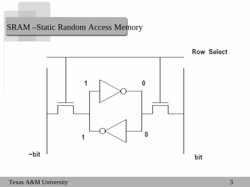
SRAM –Static Random Access Memory

4Texas A&M University
SRAM – Static Random Access Memory

5Texas A&M University
SRAM function
• When RowSelect = 1, cell can be written or read• Cell written by precharging bit/bit~ lines to required value
– Write drivers more powerful than NOT gates
• Cell read by comparing bit/bit~ lines

6Texas A&M University
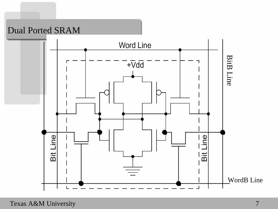
Multi-ported SRAM
• Sometimes we want to read and write at the same time• For example, registers in a processor chip
– Support 2 reads and 1 write at the same time
• Add more bit and word lines.
7Texas A&M University
Dual Ported SRAM
WordB Line
BitB
Line

8Texas A&M University
Dual Ported SRAM –Second Design

9Texas A&M University
Register cell – 2 Reads and 1 Write

10Texas A&M University
SRAM 16 words, each word = 4bits
11Texas A&M University
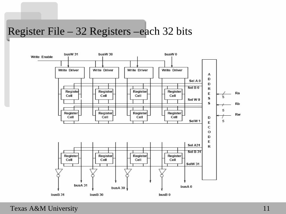
Register File – 32 Registers –each 32 bits
12Texas A&M University
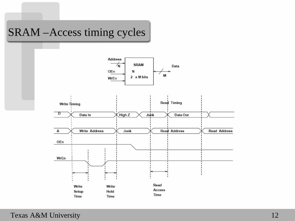
SRAM –Access timing cycles

13Texas A&M University
DRAM – Dynamic RAM

14Texas A&M University
DRAM function
• Charge on the capacitance remembers 1• Charge dissipates over time
– Over time 1 becomes 0
• Need to refresh memory• To read, Row Select = 1, charge is transferred to bit line
– Capacitor discharged– Every read requires rewriting read value back

15Texas A&M University
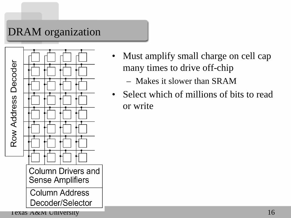
DRAM organization
16Texas A&M University
DRAM organization
• Must amplify small charge on cell cap many times to drive off-chip– Makes it slower than SRAM
• Select which of millions of bits to read or write
17Texas A&M University
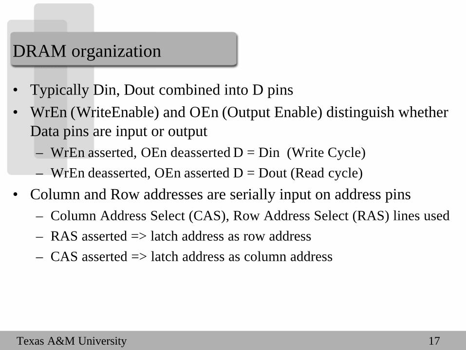
DRAM organization
• Typically Din, Dout combined into D pins• WrEn (WriteEnable) and OEn (Output Enable) distinguish whether
Data pins are input or output– WrEn asserted, OEn deasserted D = Din (Write Cycle)– WrEn deasserted, OEn asserted D = Dout (Read cycle)
• Column and Row addresses are serially input on address pins– Column Address Select (CAS), Row Address Select (RAS) lines used– RAS asserted => latch address as row address– CAS asserted => latch address as column address
18Texas A&M University
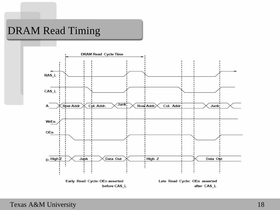
DRAM Read Timing

19Texas A&M University
DRAM Write Timing
20Texas A&M University
SRAM/DRAM comparison
• Speed– SRAM +, DRAM –– Use SRAM for cache, network buffers, etc.
• Volatility– SRAM retains data while power is on– DRAM must be refreshed every few milliseconds
• Cost– SRAM -, DRAM ++– Use DRAM for big, cheap memories
• Overhead– SRAM +, DRAM – (due to refreshing and clocks)– Use SRAM for small memories, DRAM for big

21Texas A&M University
Content Addressable Memory (CAM)
• In normal memories, we access data stored at a particular address– We give the address as input, to write/read data
• What if we want to access data by its contents?– Content addressable memories
• Used extensively in network routers/switches• Look up CAM tutorial at
http://www.pagiamtzis.com/pubs/pagiamtzis-jssc2006.pdf
22Texas A&M University
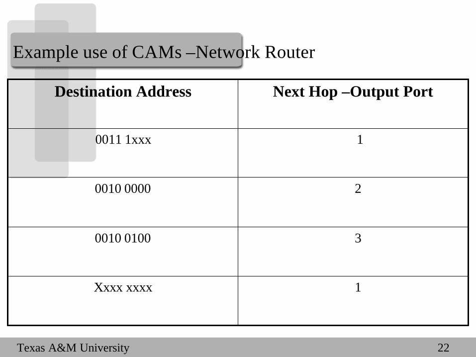
Example use of CAMs –Network Router
1Xxxx xxxx
30010 0100
20010 0000
10011 1xxx
Next Hop –Output PortDestination Address

23Texas A&M University
Example use of CAMs –network routers
• Given a destination address, we want to find which way to send the packet
• The routing table as organized as shown • We want to match the contents of the routing table entries to the
destination address to find the direction in which to send the packet• Addresses may be completely or partially specified
– Don’t cares or a concise way of representing many addresses– Saves space in the routing table

24Texas A&M University
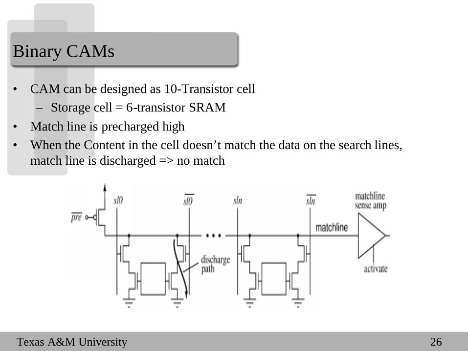
Binary CAMs
25Texas A&M University
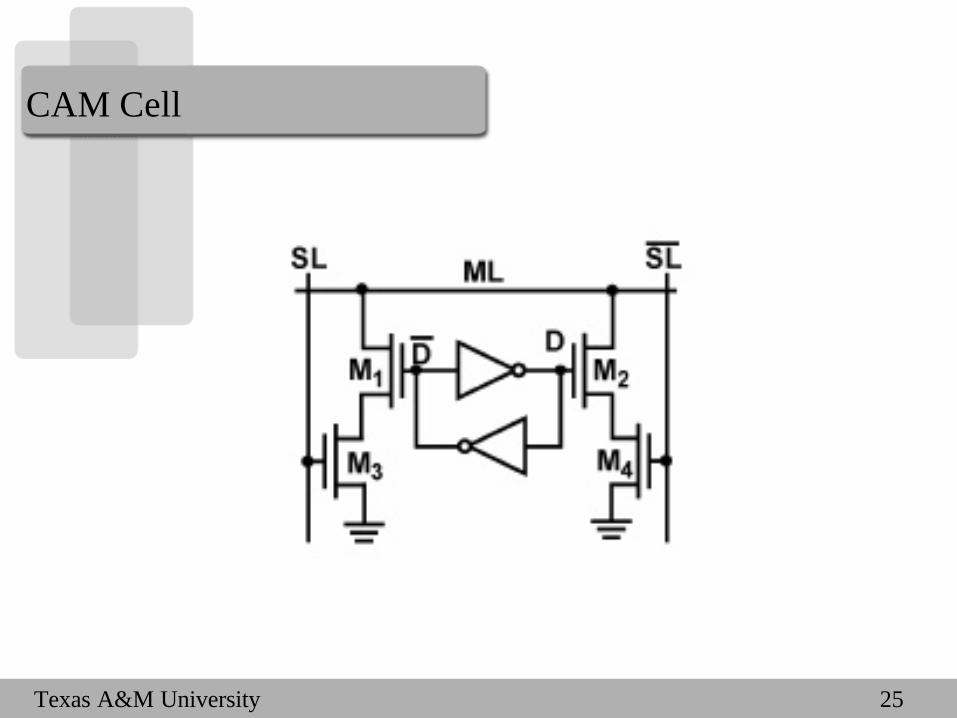
CAM Cell
26Texas A&M University
Binary CAMs
• CAM can be designed as 10-Transistor cell– Storage cell = 6-transistor SRAM
• Match line is precharged high• When the Content in the cell doesn’t match the data on the search lines,
match line is discharged => no match

27Texas A&M University
CAM architecture

28Texas A&M University
CAM architecture
• When a line matches, we can output the address or location of that content
• When multiple entries match, output the first match– Gives priority to earlier entries

29Texas A&M University
Ternary CAM
• In many applications, we need to store Don’t cares• Three states: 0, 1, X• Use two bits of actual storage to encode the three different
values• For example, use 01 = 0, 10 = 1, 00 = X

30Texas A&M University
TCAM Cell

31Texas A&M University
TCAM
• Precharge Match line high• When stored data matches search line –match line stays high
– Otherwise, match line pulled low
32Texas A&M University
Persistent memory
• SRAM/DRAM lose memory when power is turned off• More persistent memory needed for several applications
– Photos in a digital camera– Bootable code or settings on circuits
• Flash memory used for these applications– Memory persists across power on/off cycles– Small size
33Texas A&M University
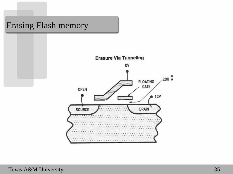
Flash memory
• Charge stored on an isolated conductor –called floating gate• Charge has no path to dissipate• The charge on the floating gate controls the current flowing
between source and drain– Tells if a 1 or 0 is in the cell
• To erase the cell, a reverse voltage is applied between the drain and the controlling gate– Charge is dissipated through tunneling

34Texas A&M University
Flash Memory Cell
35Texas A&M University
Erasing Flash memory
36Texas A&M University
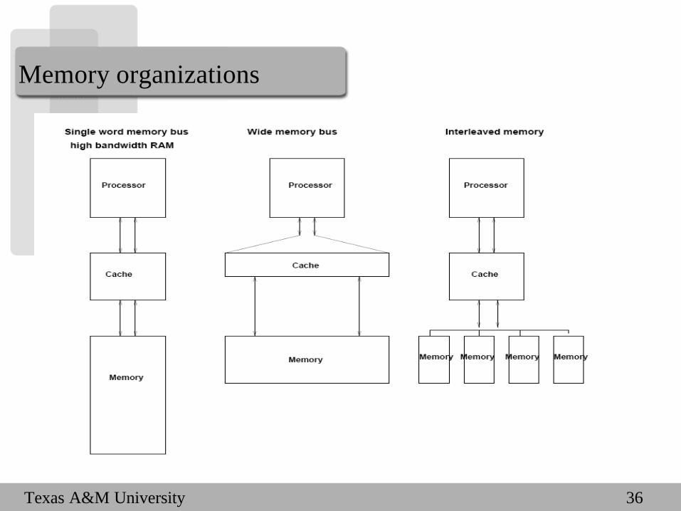
Memory organizations
37Texas A&M University
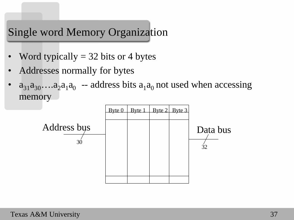
Single word Memory Organization
• Word typically = 32 bits or 4 bytes• Addresses normally for bytes• a31a30….a2a1a0 -- address bits a1a0 not used when accessing
memory
Data bus30
32
Address bus
Byte 0 Byte 1 Byte 2 Byte 3

38Texas A&M University
Wide Memory Organization
• Memory is slow compared to cache/processor• There is normally locality in memory accesses
– If you access location A, likely to access A+1, A+2…– Why not access multiple words at a time to reduce access times
28128
Address bus
Word 0 Word 1 Word 2 Word 3
Data bus

39Texas A&M University
Interleaved Memory Organization
• Organize memory into banks• Each bank can be separately accessed• Data is distributed across multiple banks to increase parallelism
Address Bus
Data Bus

40Texas A&M University
Interleaved Memory Organization
• Can keep multiple banks busy at the same time• Give address to first bank, then a different address to second
bank…so on• Data accesses will be in different stages in different banks• Somewhat like pipelined…• Consider 4-bank memory with each bank organized as 2-word wide• 3 bits a2a1a0 needed to address the 2-words (8 bytes)• Each bank is addressed by the same a4a3 bits. Bank 0 will have a4a3
= 00, bank 1 will have a4a3 = 11….
41Texas A&M University
Interleaved Memory Organization
• Can function as a wide-word access if we give the consecutive addresses to different banks
• Can also access different words from different banks that are not consecutive– As long as there are no bank conflicts
• When will have bank conflicts in our example?• Flash memories/drives have wide bank organizations
– An example drive: with 2048 banks with each bank holding 512-byte sector
– Access 1MB memory fast