memory interface - · pdf file• simple or complex, ... • this chapter explains how...
TRANSCRIPT

Memory Interface
Introduction
• Simple or complex, every microprocessor-
based system has a memory system.
• Almost all systems contain two main types of
memory: read-only memory (ROM) and
random access memory (RAM) or read/write
memory.
• This chapter explains how to interface both
memory types to the Intel family of
microprocessors.

MEMORY DEVICES
• Before attempting to interface memory to the
microprocessor, it is essential to understand
the operation of memory components.
• In this section, we explain functions of the
four common types of memory:
– Read-only memory (ROM)
– Flash memory (EEPROM)
– Static random access memory (SRAM)
– Dynamic random access memory (DRAM)
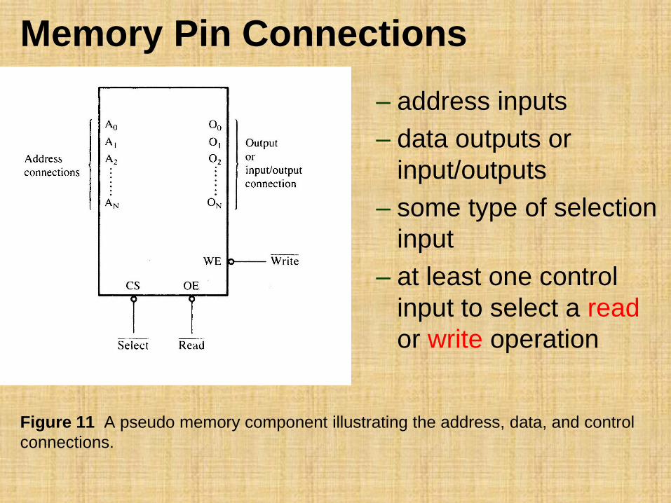
Figure 11 A pseudo memory component illustrating the address, data, and control
connections.
Memory Pin Connections
– address inputs
– data outputs or
input/outputs
– some type of selection
input
– at least one control
input to select a read
or write operation

Address Connections
• Memory devices have address inputs to
select a memory location within the device.
• Almost always labeled from A0, the least
significant address input, to An
– where subscript n can be any value
– always labeled as one less than total number
of address pins
• A memory device with 10 address pins has
its address pins labeled from A0 to A9.
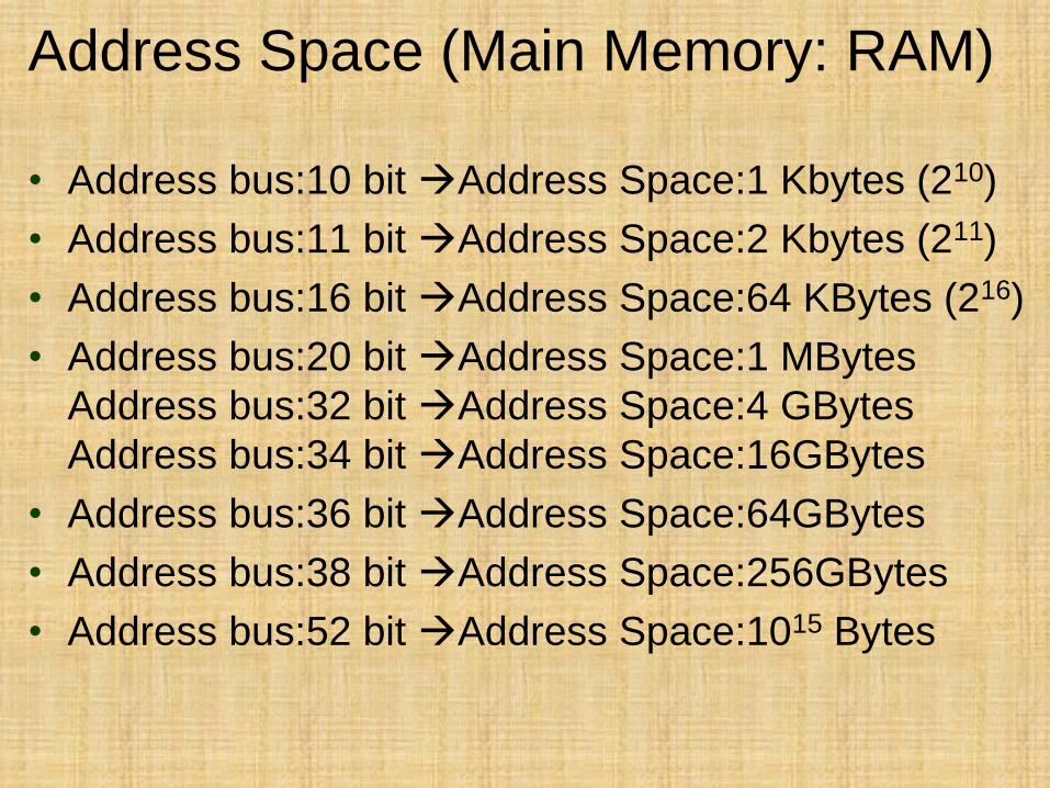
Address Space (Main Memory: RAM)
• Address bus:10 bit Address Space:1 Kbytes (210)
• Address bus:11 bit Address Space:2 Kbytes (211)
• Address bus:16 bit Address Space:64 KBytes (216)
• Address bus:20 bit Address Space:1 MBytes
Address bus:32 bit Address Space:4 GBytes
Address bus:34 bit Address Space:16GBytes
• Address bus:36 bit Address Space:64GBytes
• Address bus:38 bit Address Space:256GBytes
• Address bus:52 bit Address Space:1015 Bytes

• The number of address pins on a memory
device is determined by the number of
memory locations found within it.
• Today, common memory devices have
between 1K (1024) to 1G (1,073,741,824)
memory locations.
– with 4G and larger devices on the horizon
• A 1K memory device has 10 address pins.
– therefore, 10 address inputs are required to
select any of its 1024 memory locations

• It takes a 10-bit binary number to select any
single location on a 1024-location device.
– 1024 different combinations
– if a device has 11 address connections, it
has 2048 (2K) internal memory locations
• The number of memory locations can be
extrapolated from the number of pins.

Data Connections
• All memory devices have a set of data
outputs or input/outputs.
– today, many devices have bidirectional
common I/O pins
– data connections are points at which data are
entered for storage or extracted for reading
• Data pins on memory devices are labeled D0
through D7 for an 8-bit-wide memory device.
• An 8-bit-wide memory device is often called a
byte-wide memory.
– most devices are currently 8 bits wide,
– some are 16 bits, 4 bits, or just 1 bit wide
• Catalog listings of memory devices often refer
to memory locations times bits per location.
– a memory device with 1K memory locations
and 8 bits in each location is often listed as
a 1K 8 by the manufacturer
• Memory devices are often classified
according to total bit capacity.
Selection Connections
• Each memory device has an input that selects
or enables the memory device.
– sometimes more than one
• This type of input is most often called a chip
select (G2A) chip enable (CE) or simply
select (S) input.
• RAM memory generally has at least one or
input, and ROM has at least one
• If more than one CE connection is present,
all must be activated to read or write data.
Control Connections
• All memory devices have some form of control
input or inputs.
– ROM usually has one control input, while RAM
often has one or two control inputs
• Control input often found on ROM is the
output enable or gate connection, which
allows data flow from output data pins.
• The OE connection enables and disables a
set of three-state buffers located in the device
and must be active to read data.
• RAM has either one or two control inputs.
– if one control input, it is often called R/W
• If the RAM has two control inputs, they are
usually labeled WE (or W ), and OE (or G ).
– write enable must be active to perform memory
write, and OE active to perform a memory read
– when the two controls are present, they must
never both be active at the same time
• If both inputs are inactive, data are neither
written nor read.
– the connections are at their high-impedance state
ROM Memory
• Read-only memory (ROM) permanently
stores programs/data resident to the system.
– and must not change when power disconnected
• Often called nonvolatile memory, because
its contents do not change even if power is
disconnected.
• A device we call a ROM is purchased in mass
quantities from a manufacturer.
– programmed during fabrication at the factory
• The EPROM (erasable programmable read-
only memory) is commonly used when
software must be changed often.
– or when low demand makes ROM uneconomical
– for ROM to be practical at least 10,000 devices
must be sold to recoup factory charges
• An EPROM is programmed in the field on a
device called an EPROM programmer.
• Also erasable if exposed to high-intensity
ultraviolet light.
– depending on the type of EPROM
• PROM memory devices are also available,
although they are not as common today.
• The PROM (programmable read-only
memory) is also programmed in the field by
burning open tiny NI-chrome or silicon oxide
fuses.
• Once it is programmed, it cannot be erased.

• A newer type of read-mostly memory
(RMM) is called the flash memory.
– also often called an EEPROM (electrically
erasable programmable ROM)
– EAROM (electrically alterable ROM)
– or a NOVRAM (nonvolatile RAM)
• Electrically erasable in the system, but they
require more time to erase than normal RAM.
• The flash memory device is used to store
setup information for systems such as the
video card in the computer.

• Flash has all but replaced the EPROM in
most computer systems for the BIOS.
– some systems contain a password stored
in the flash memory device
• Flash memory has its biggest impact in
memory cards for digital cameras and
memory in MP3 audio players.
• Figure 2 illustrates the 2716 EPROM, which is
representative of most common EPROMs.
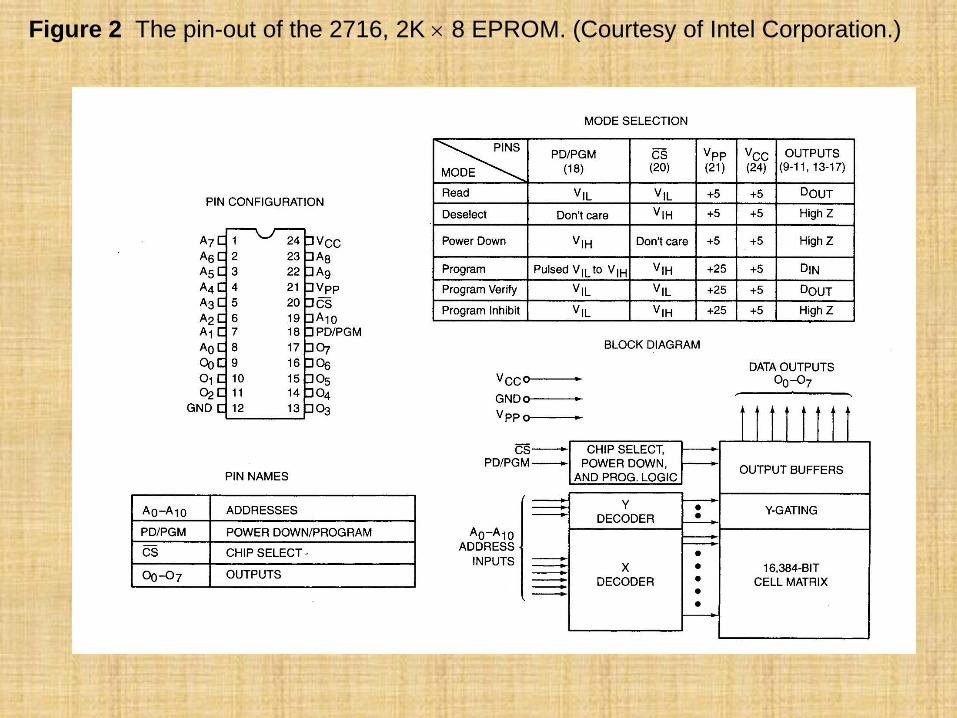
Figure 2 The pin-out of the 2716, 2K 8 EPROM. (Courtesy of Intel Corporation.)

• Figure 3 illustrates the timing diagram for the
2716 EPROM.
• The VPP pin must be placed at a logic 1 level
for data to be read from the EPROM.
• In some cases, the VPP pin is in the same
position as the WE pin on the SRAM.
• This will allow a single socket to hold either
an EPROM or an SRAM.
– an example is the 27256 EPROM and 62256
SRAM, both 32K 8 devices with the same pin-
out, except for VPP on the EPROM and WE on
the SRAM.
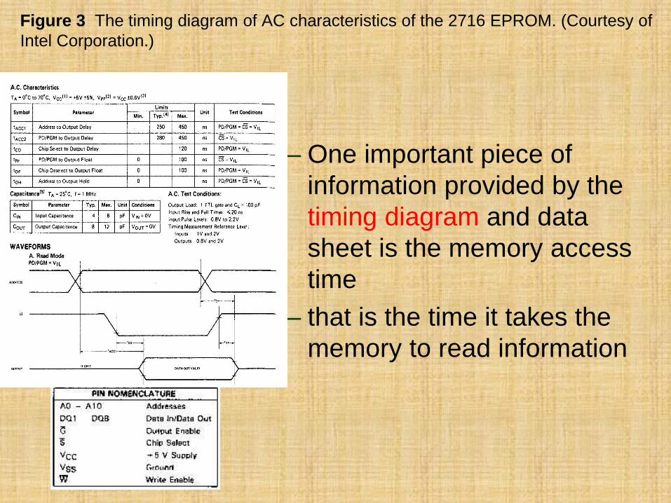
Figure 3 The timing diagram of AC characteristics of the 2716 EPROM. (Courtesy of
Intel Corporation.)
– One important piece of
information provided by the
timing diagram and data
sheet is the memory access
time
– that is the time it takes the
memory to read information
• The basic speed of this EPROM is 450 ns.
– recall that 8086/8088 operated with a 5 MHz clock
allowed memory 460 ns to access data
• This type of component requires wait states
to operate properly with 8086/8088 because
of its rather long access time.
– if wait states are not desired, higher-speed
EPROMs are available at additional cost
– EPROM memory is available with access times
of as little as 100 ns
• Obviously, wait states are required in modern
microprocessors for any EPROM device.
Static RAM (SRAM) Devices
• Static RAM memory devices retain data for
as long as DC power is applied.
• Because no special action is required to retain
data, these devices are called static memory.
– also called volatile memory because they will
not retain data without power
• The main difference between ROM and RAM
is that RAM is written under normal operation,
whereas ROM is programmed outside the
computer and normally is only read.
• Fig 4 illustrates the 4016 SRAM,
– a 2K 8 read/write memory
• This device is representative of all SRAM
devices.
– except for the number of address and data
connections.
• The control inputs of this RAM are slightly
different from those presented earlier.
– however the control pins function exactly the
same as those outlined previously
• Found under part numbers 2016 and 6116.

Figure 4 The pin-out of the TMS4016, 2K 8 static RAM (SRAM). (Courtesy of
Texas Instruments Incorporated.)
– SRAM is used when the
size of the read/write
memory is relatively
small
– today, a small memory
is less than 1M byte
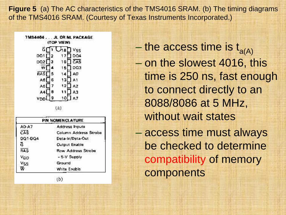
Figure 5 (a) The AC characteristics of the TMS4016 SRAM. (b) The timing diagrams
of the TMS4016 SRAM. (Courtesy of Texas Instruments Incorporated.)
– the access time is ta(A)
– on the slowest 4016, this
time is 250 ns, fast enough
to connect directly to an
8088/8086 at 5 MHz,
without wait states
– access time must always
be checked to determine
compatibility of memory
components

FIGURE 5 (a) The AC characteristics of the TMS4016 SRAM.
(b) The timing diagrams of the TMS4016 SRAM. (Courtesy of
Texas Instruments Incorporated.)


• Figure 6 illustrates pin-outs of the 62256, 32K
8 static RAM.
• Packaged in a 28-pin integrated circuit
• Available with access times of 120 or 150 ns.
• Other common SRAM devices are
– 8K 8; 128K 8; 256K 8
– 512K 8; 1M 8
• Access times can be as low as 1.0 ns for
SRAM used in computer cache memory.
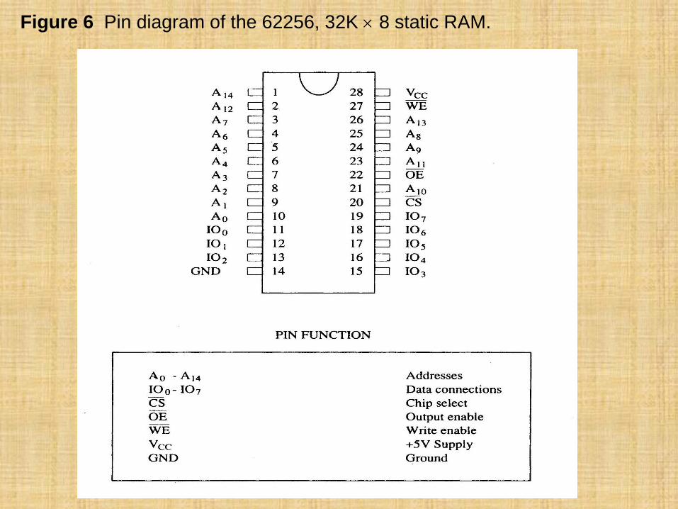
Figure 6 Pin diagram of the 62256, 32K 8 static RAM.

Static Memory Interfacing
• The general procedure of static memory
interfacing with 8086 as follows:
– Arrange the available memory chips so as to
obtain 16-bit data bus width. The upper 8-bit bank
is called ‘odd address memory bank’ and the
lower 8-bit bank is called ‘even address memory
bank’.
– Connect available memory address lines of
memory chips with those of the microprocessor
and also connect the memory RD and WR inputs
to the corresponding processor control signals.
Connect the 16-bit data bus of the memory bank
with that of the microprocessor 8086.

Static Memory Interfacing
– The remaining address lines of the
microprocessor, BHE and Ao are used for
decoding the required chip select signals for the
odd and even memory banks. The CS of memory
is derived from the output of the decoding circuit.
– As a good and efficient interfacing practice, the
address map of the system should be continuous
as far as possible
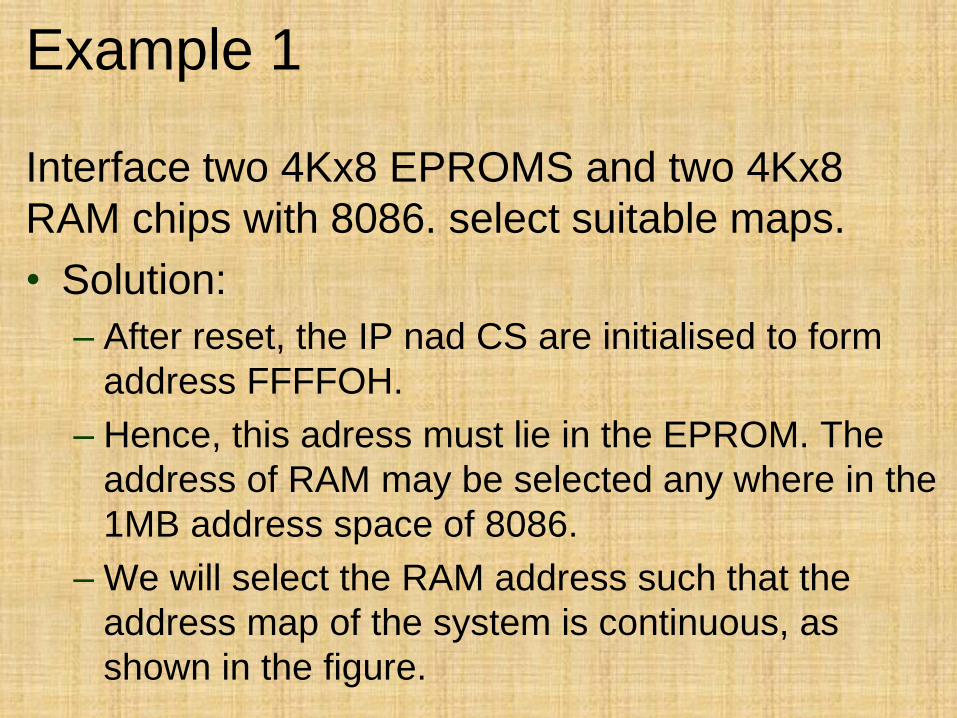
Example 1
Interface two 4Kx8 EPROMS and two 4Kx8
RAM chips with 8086. select suitable maps.
• Solution:
– After reset, the IP nad CS are initialised to form
address FFFFOH.
– Hence, this adress must lie in the EPROM. The
address of RAM may be selected any where in the
1MB address space of 8086.
– We will select the RAM address such that the
address map of the system is continuous, as
shown in the figure.
Example 1
Interface two 4Kx8 EPROMS and two 4Kx8
RAM chips with 8086. select suitable maps.
• Solution:
– Total 8K bytes of EPROM need 13 address lines
Ao-A12 (since 2^13=8K).
– Adress lines A13 – A19 are used for decoding to
generate the chip select.
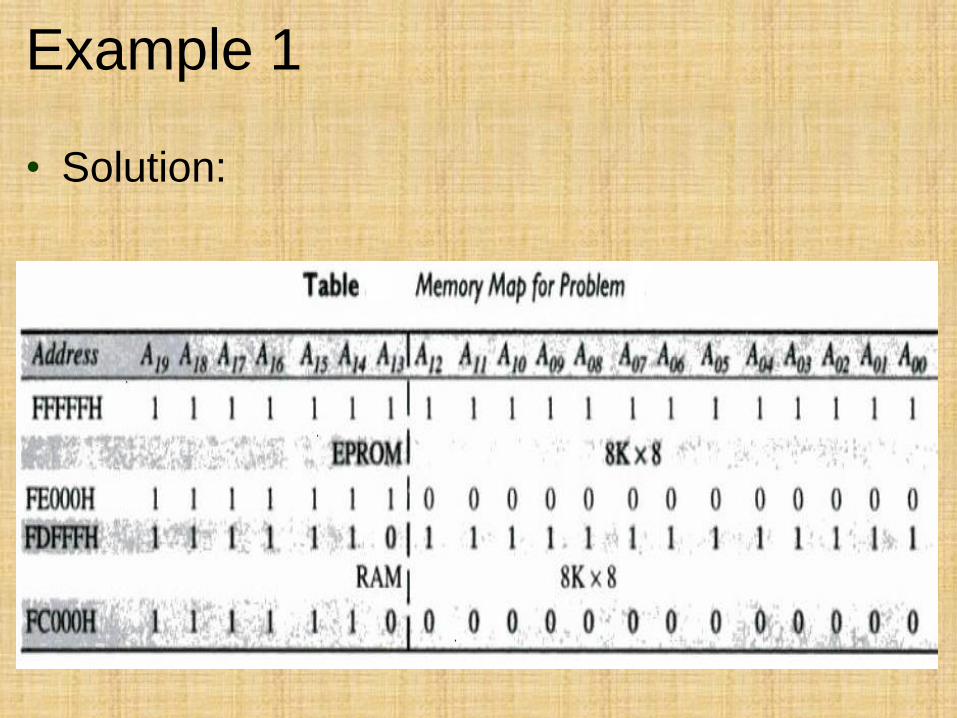
Example 1
• Solution:
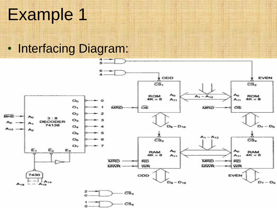
Example 1
• Interfacing Diagram:

Example 1• Solution:
– The memory system in this example contains in
total four 4Kx8 memory chip.
– The two 4Kx8 chips of RAM and ROM are
arranged in parallel to obtain 16-bit data bus
– width.
– Ao is 0, i.e. the address is even and is in RAM,
then the lower RAM chip is selected indicating 8-
bit transfer at an even address.
– If Ao is 1, i.e. the address is odd and is in RAM,
the BHE goes low, the upper RAM chip is
selected, further indicating that the 8-bit transfer is
at an odd address.

Example 1
• Solution:
– The selection of chips here takes place as shown
in table.

Dynamic RAM (DRAM) Memory
• Available up to 256M 8 (2G bits).
• DRAM is essentially the same as SRAM,
except that it retains data for only 2 or 4 ms
on an integrated capacitor.
• After 2 or 4 ms, the contents of the DRAM
must be completely rewritten (refreshed).
– because the capacitors, which store a logic 1
or logic 0, lose their charges

• In DRAM, the entire contents are refreshed
with 256 reads in a 2- or 4-ms interval.
– also occurs during a write, a read, or during a
special refresh cycle
• DRAM requires so many address pins that
manufacturers multiplexed address inputs.
• Figure 7 illustrates a 64K 4 DRAM, the
TMS4464, which stores 256K bits of data.
– note it contains only eight address inputs where
it should contain 16—the number required to
address 64K memory locations

Figure 7 The pin-out of the TMS4464, 64K 4 dynamic RAM (DRAM). (Courtesy of
Texas Instruments Incorporated.)
– 16 address bits can be
forced into eight address
pins in two 8-bit
increments
– this requires two special
pins: the column address
strobe (CAS) and row
address strobe (RAS)
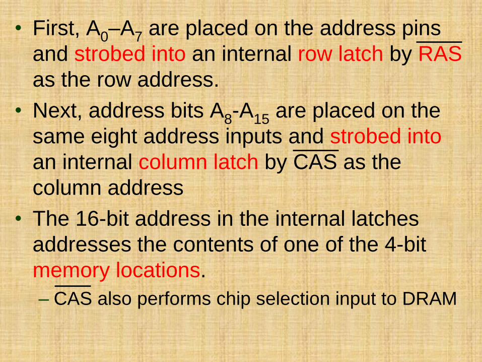
• First, A0–A7 are placed on the address pins
and strobed into an internal row latch by RAS
as the row address.
• Next, address bits A8-A15 are placed on the
same eight address inputs and strobed into
an internal column latch by CAS as the
column address
• The 16-bit address in the internal latches
addresses the contents of one of the 4-bit
memory locations.
– CAS also performs chip selection input to DRAM

Figure 8 RAS, CAS and address input timing for the TMS4464 DRAM. (Courtesy of
Texas Instruments Incorporated.)
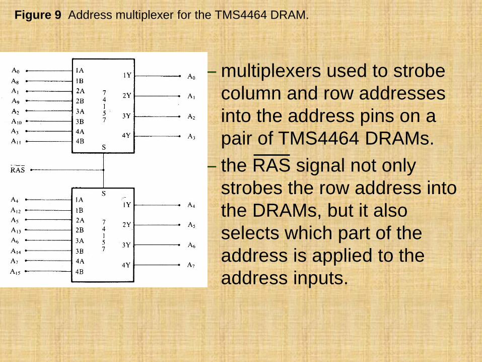
Figure 9 Address multiplexer for the TMS4464 DRAM.
– multiplexers used to strobe
column and row addresses
into the address pins on a
pair of TMS4464 DRAMs.
– the RAS signal not only
strobes the row address into
the DRAMs, but it also
selects which part of the
address is applied to the
address inputs.
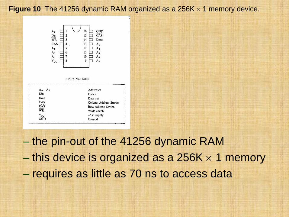
Figure 10 The 41256 dynamic RAM organized as a 256K 1 memory device.
– the pin-out of the 41256 dynamic RAM
– this device is organized as a 256K 1 memory
– requires as little as 70 ns to access data
• DRAM is often placed on small boards called
SIMMs (Single In-Line Memory Modules).
• The 30-pin SIMM is organized most often as
1M 8 or 1M 9, and 4M 8 or 4M 9.
– illustrated in Fig 10–11 is a 4M 9
– the ninth bit is the parity bit
• Also shown is a newer 72 pin SIMM.
• 72-pin SIMMs are often organized as 1M 32
or 1M 36 (with parity).
• Fig 10–11 illustrates a 4M 36 SIMM, which
has 16M bytes of memory

Figure 11 The pin-outs of the 30-pin and 72-pin SIMM. (a) A 30-pin SIMM organized
as 4M 9 and (b) a 72-pin SIMM organized as 4M 36.
• Pentium–Pentium 4 microprocessors have a
64-bit wide data bus, which precludes use of
the 8-bit-wide SIMMs described here.
– 72-pin SIMMs are cumbersome as they must be
paired to obtain a 64-bit-wide data connection
• 64-bit-wide DIMMs (Dual In-line Memory
Modules) have become the standard.
• The memory on these modules is organized
as 64 bits wide.
• Common sizes available are from 16M bytes
(2M 64) to 1G bytes (128M 64).

Figure 12 The pin-out of a 168-pin DIMM.
– The DIMM module is available in DRAM, EDO,
SDRAM, and DDR (double-data rate) forms, with
or without an EPROM.
– The EPROM provides information to the system
on the size and the speed of the memory device
for plug-and-play applications.

• Another type is the RIMM memory module
from RAMBUS Corporation,
– this memory type has faded from the market
• The latest DRAM is the DDR (double-data
rate) memory device and DDR2.
– DDR transfers data at each edge of the clock,
making it operate at twice the speed of SDRAM
• Many wait states are still required to operate
this type of memory, but it can be much faster
than normal SDRAM memory, including
RDRAM.

THE END