mems fabrication by thomas szychowski. mems overview micron level mechanical parts made from...
TRANSCRIPT
MEMS Fabrication
By
Thomas Szychowski
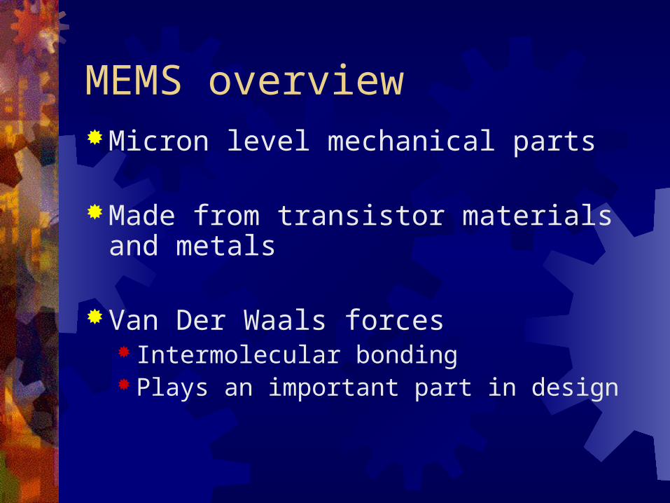
MEMS overviewMicron level mechanical parts
Made from transistor materials and metals
Van Der Waals forces Intermolecular bonding Plays an important part in design
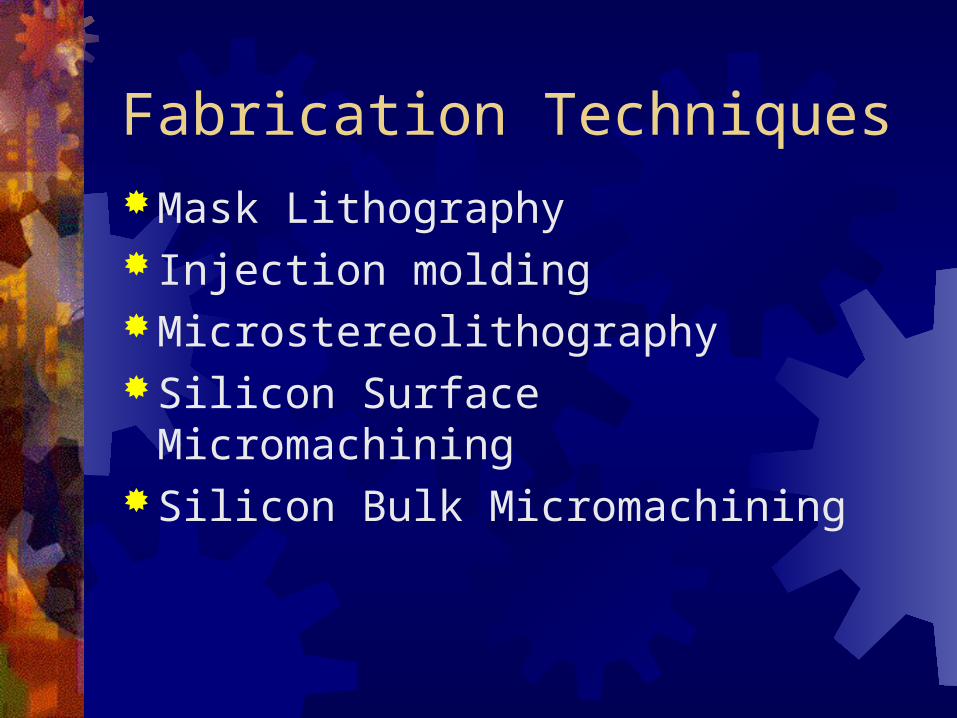
Fabrication TechniquesMask Lithography Injection moldingMicrostereolithographySilicon Surface MicromachiningSilicon Bulk Micromachining
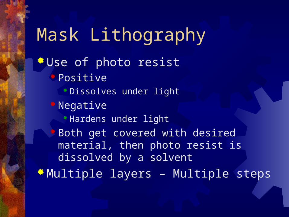
Mask LithographyUse of photo resist
Positive Dissolves under light
Negative Hardens under light
Both get covered with desired material, then photo resist is dissolved by a solvent
Multiple layers – Multiple steps
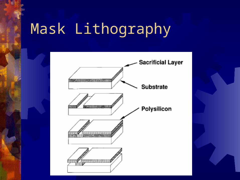
Mask Lithography
Injection Molding
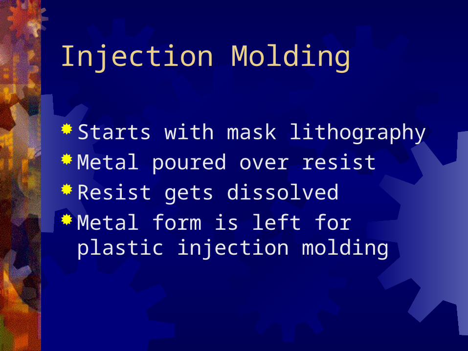
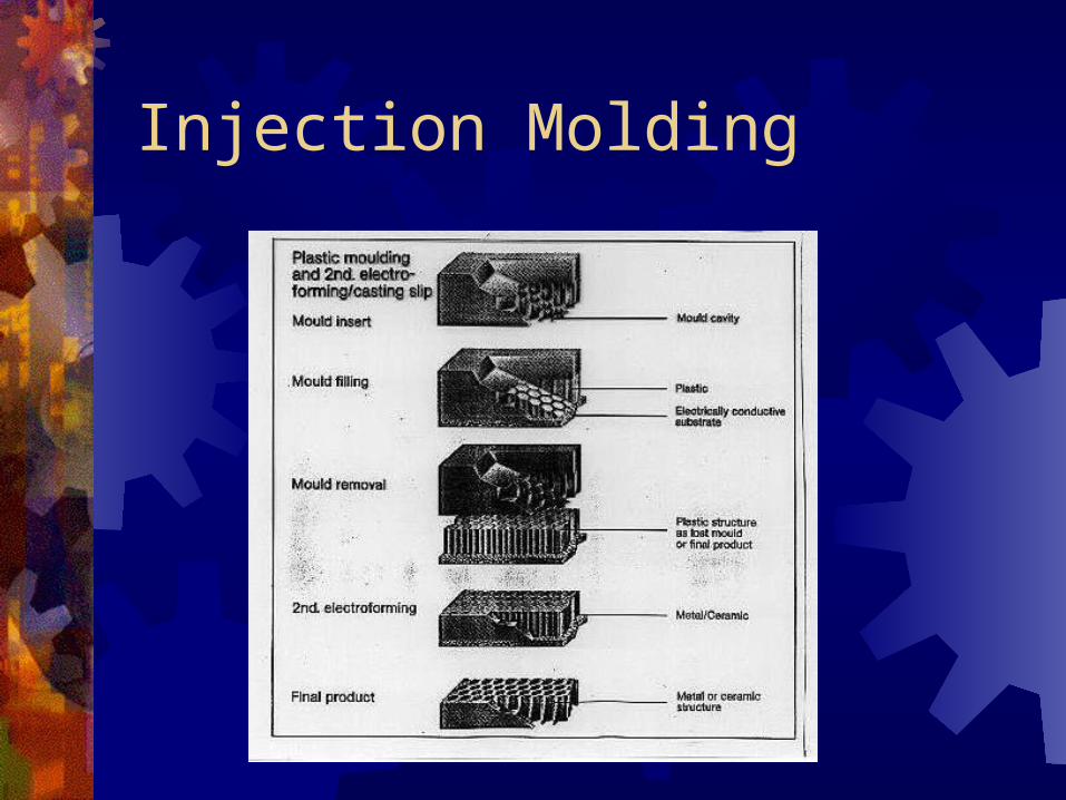
Starts with mask lithographyMetal poured over resistResist gets dissolvedMetal form is left for plastic injection
molding
Injection Molding
Microstereolithography
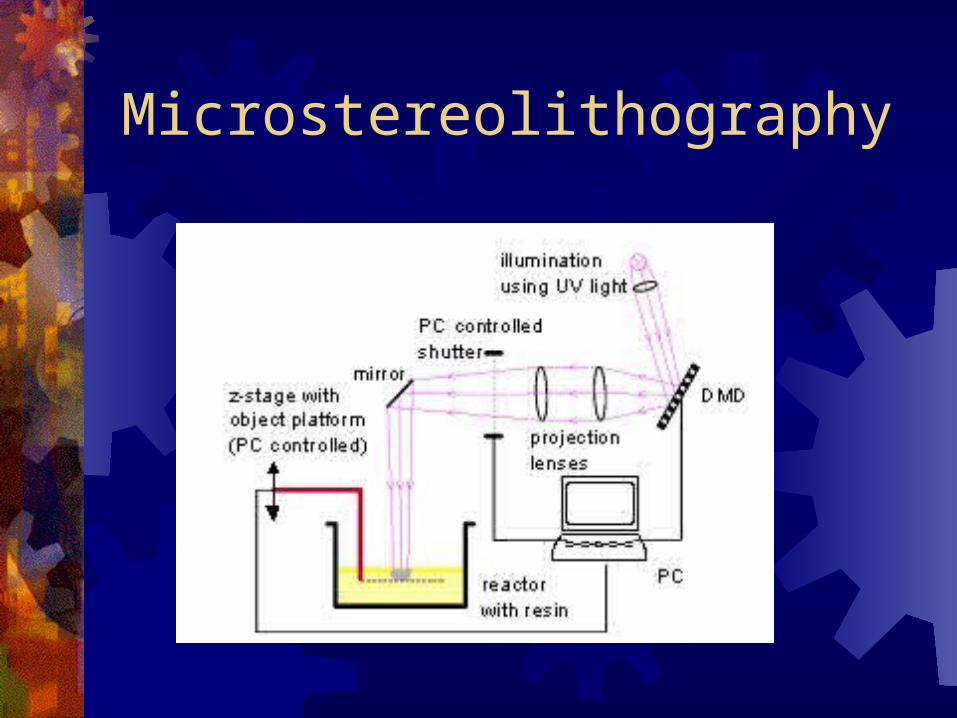
Similar principal to mask lithography, but for 3D pieces Uses an “active mask”
Not a physical mask Utilizes a photo-reactive acrylic resin Each layer image projected through a DMD(digital mirror
device) Projected into the resin
Uses lenses Resin that is illuminated, Cross-links and hardens Piece is then covered in a hardened layer
Microstereolithography
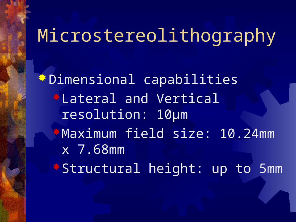
Dimensional capabilitiesLateral and Vertical resolution: 10μm Maximum field size: 10.24mm x
7.68mm Structural height: up to 5mm
Microstereolithography
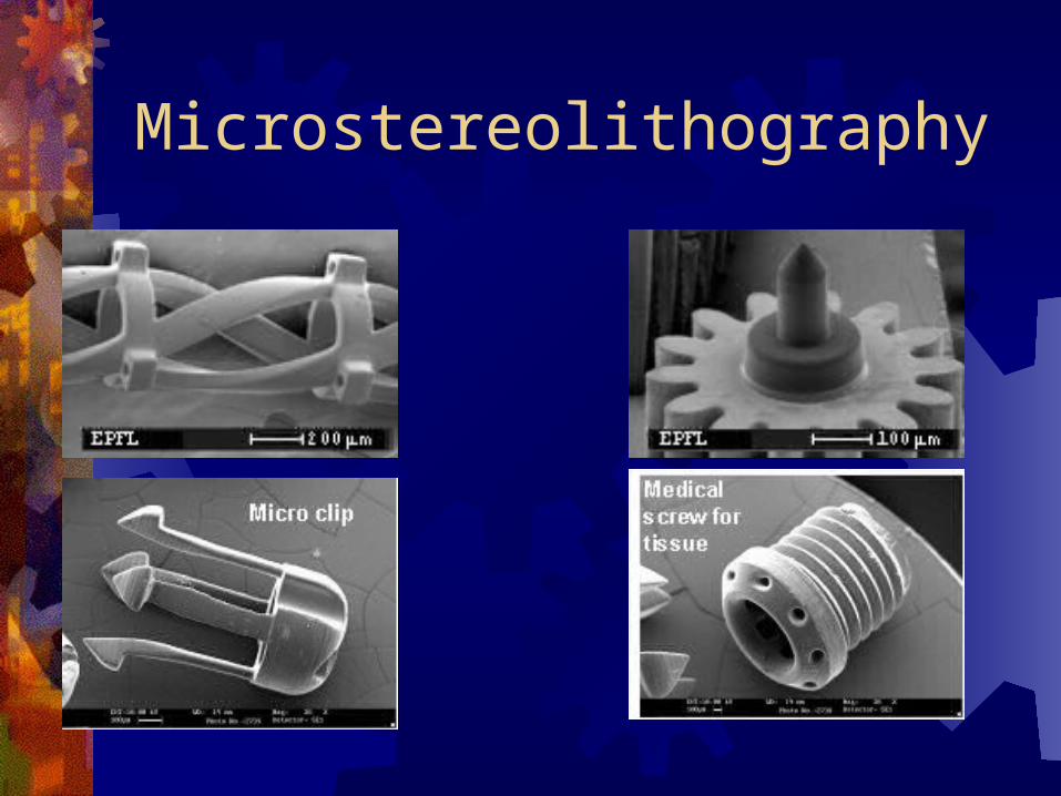
Microstereolithography
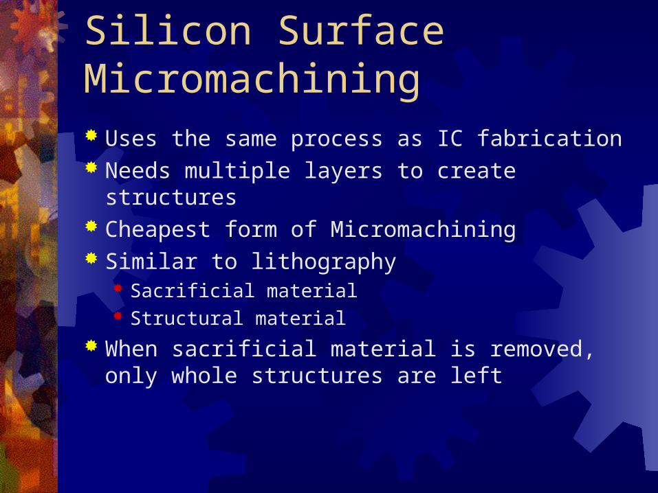
Silicon Surface Micromachining Uses the same process as IC fabrication Needs multiple layers to create structures Cheapest form of Micromachining Similar to lithography
Sacrificial material Structural material
When sacrificial material is removed, only whole structures are left
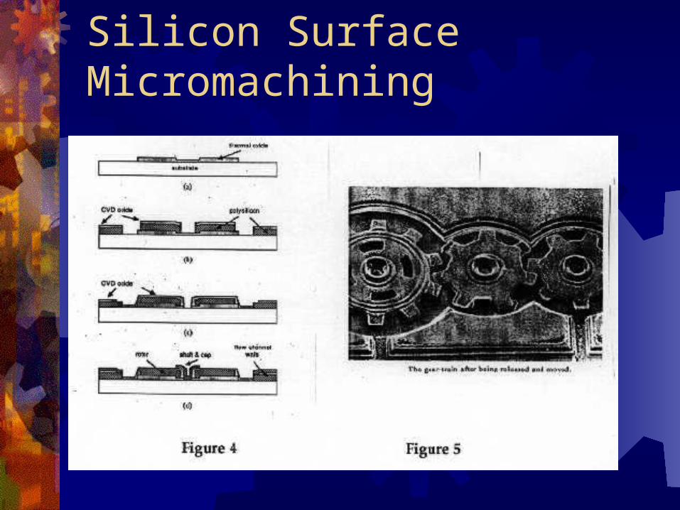
Silicon Surface Micromachining
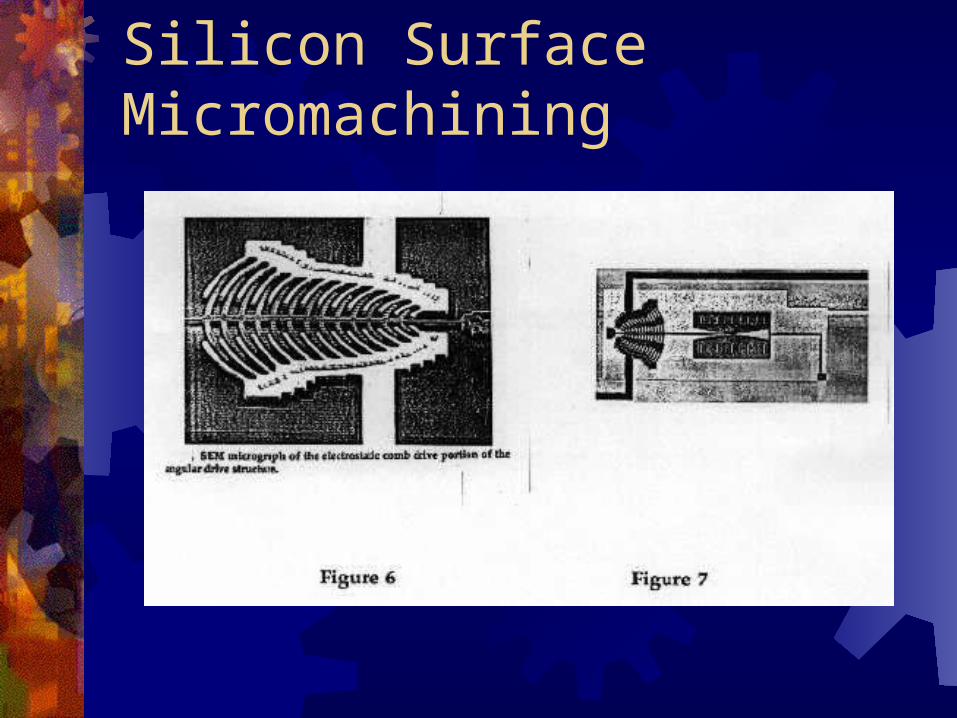
Silicon Surface Micromachining
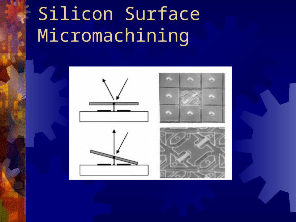
Silicon Surface Micromachining
Silicon Bulk Micromachining
Done with Crystalline silicon Constructed using etch stop planes Chemical process Anisotropic Etching
Speed dependent – Directional etch in different crystallographic directions at
different rates Slower directions create and etch stop plane
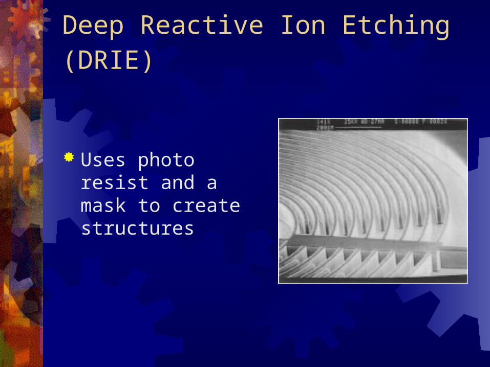
Deep Reactive Ion Etching (DRIE)
Uses photo resist and a mask to create structures
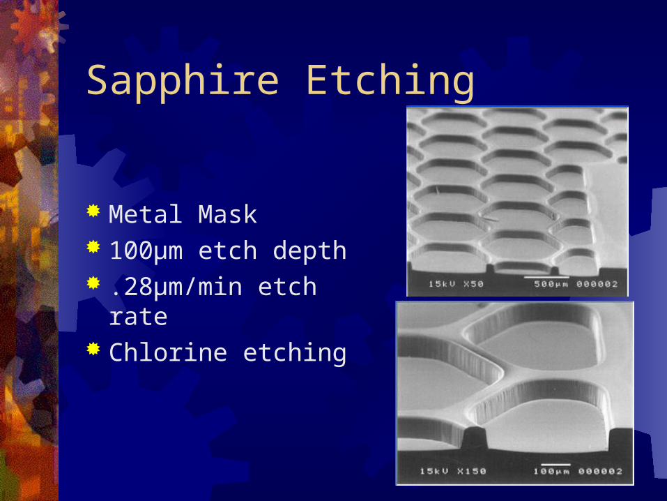
Sapphire Etching
Metal Mask 100µm etch depth .28µm/min etch rate Chlorine etching
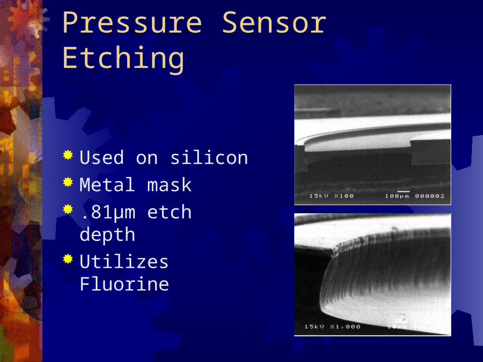
Pressure Sensor Etching
Used on silicon Metal mask .81µm etch depth Utilizes Fluorine
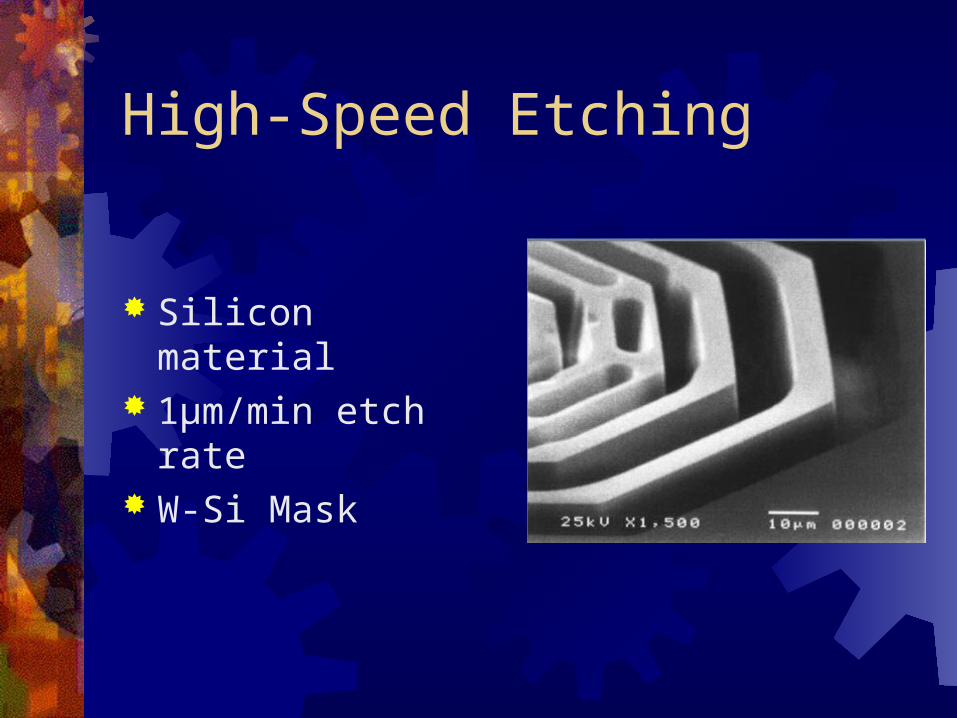
High-Speed Etching
Silicon material 1µm/min etch rate W-Si Mask
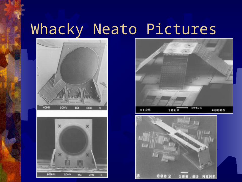
Whacky Neato Pictures

Questions
?

References http://home.earthlink.net/~trimmerw/mems/tour.html http://home.earthlink.net/~trimmerw/mems/BM_bulk.h
tml http://www.samcointl.com/apps/mems.html http://www.cmf.rl.ac.uk/latest/msl.html http://www.chemguide.co.uk/atoms/bonding/vdw.html “Micromachining for Optical and Optoelectronic
Systems”. MING C. WU