meptec 2015 – high reliability die attach solution for ...meptec.org/resources/mar 2015 henkel...
TRANSCRIPT

MEPTEC 2015 – High Reliability Die Attach Solution for Automotive Applications
Andrew Laib and Mina Chow-Taing MARCH 2015
MEPTEC 2015 – High Reliability Die Attach Solution for Automotive Applications
Andrew Laib and Mina Chow-Taing MARCH 2015

2
1. Objectives
2. Market & Package Trend
3. Current Material Challenges & Needs
4. Control Flow
5. General Process
6. Product Portfolio
7. High Reliability Die Attach Solution
8. Summary
9. Global Contacts
10.Appendix
Contents
MEPTEC 2015- cDAF3/11/15

3
• Introduce cDAF value proposition.
• Introduce cDAF product portfolio.
• cDAF as die attach solution for automotive applications.
Objectives
MEPTEC 2015- cDAF3/11/15
4
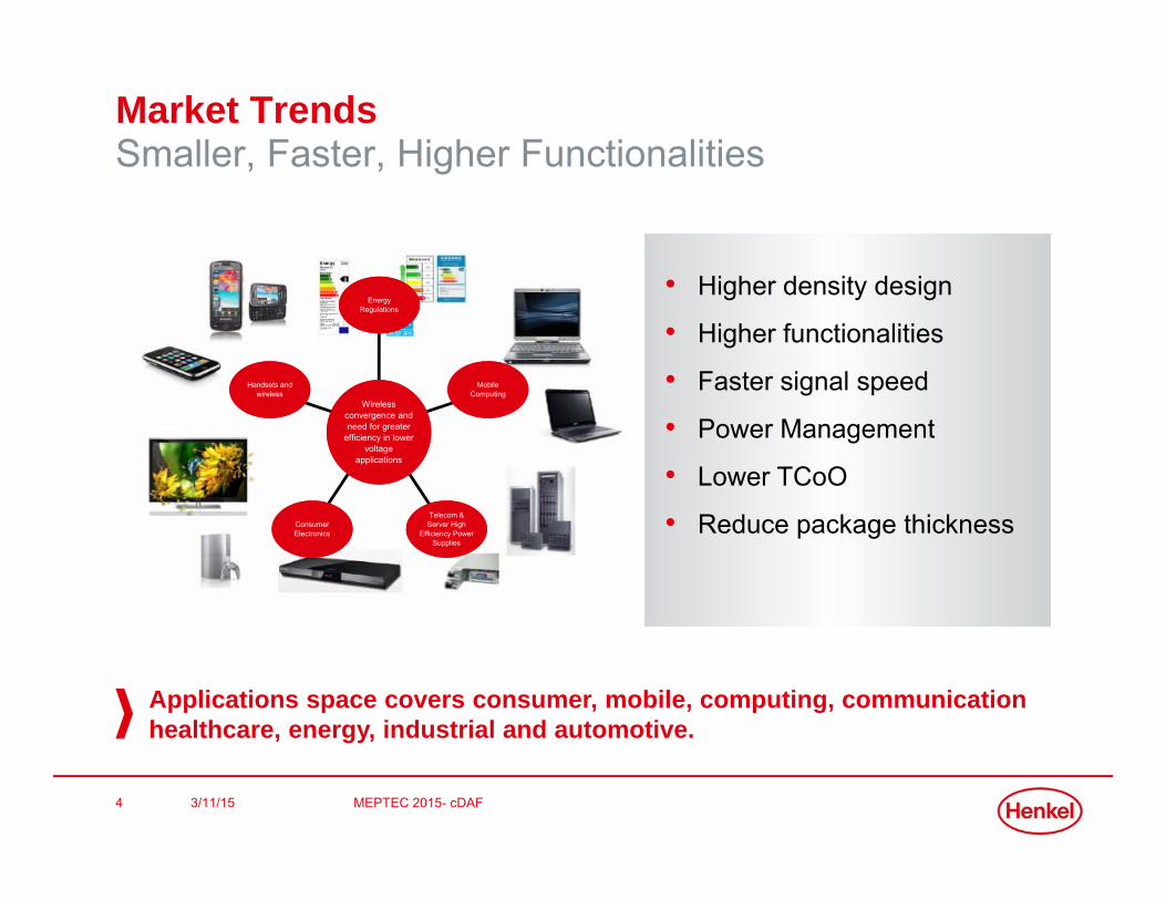
Market TrendsSmaller, Faster, Higher Functionalities
Applications space covers consumer, mobile, computing, communication healthcare, energy, industrial and automotive.
Wireless convergence and need for greater
efficiency in lower voltage
applications
Wireless convergence and need for greater
efficiency in lower voltage
applications
Energy Regulations
Energy Regulations
Mobile Computing
Mobile Computing
Telecom & Server High
Efficiency Power Supplies
Telecom & Server High
Efficiency Power Supplies
Consumer ElectronicsConsumer Electronics
Handsets and wireless
Handsets and wireless
• Higher density design
• Higher functionalities
• Faster signal speed
• Power Management
• Lower TCoO
• Reduce package thickness
MEPTEC 2015- cDAF3/11/15

5
Package Trends – WirebondedHigher Functionality & Efficiency
• Miniaturized packages (QFN, DFN, SOs)• Increased die-to-pad ratio• In some case D/P ratio close to 1.0
• Thinner packages (QFN, SO, QFP)• Packages <0.3mm• Thinner die <75um• Thinner DA bondline thickness <20um
• Higher density packages• Multi-dies packages
• SiP – LGA/PBGA
MEPTEC 2015- cDAF3/11/15

6
Current Material ChallengesConducting Die Attach Paste
• Dispensing: Optimize dispense patterns for various die sizes – 0.2 x0.2 mm to >10x10mm.
• Fillet & Bleed: Forces engineers to have a minimum keep out zone around die.
• Bondline Control: Specially for smaller die BLT control is challenging and leads to die tilt.
• Kerf Creep: For thinner wafers uneven fillet height can lead to kerf creep.
Paste
Cross section of typical paste die attach.
Typical paste-based die attach.
MEPTEC 2015- cDAF3/11/15

7
New Material NeedsWhat does the market really need moving forward?
• Lower Cost
• Higher Reliability
• Zero Delamination
• Zero Bleed
• Minimal fillet
• Consistent BLT control
• Thin Wafer handling capability
• Low to no outgassing
• Drop in solution
MEPTEC 2015- cDAF3/11/15

8
Control FlowEnables Miniaturization
Reduced footprint Shorter interconnection Faster signal speed
Less Au wire, leadframe, EMC used Lower TCoO
With Fillet Controlled Fillet
MEPTEC 2015- cDAF3/11/15

9
Control FlowEnables Thin Wafer Handling
• Thinner wafer handling enabled• Consistent Thinner bondlines achieved• Eliminated Fillet• Eliminated bleed
Die Attach PasteDie Attach Paste
Package with Fillet
Die Attach FilmDie Attach Film
Controlled Fillet Height
Si Die >200ums Si Die 75ums
MEPTEC 2015- cDAF3/11/15

10
Control FlowTechnology Enabler & Lowers TCoO
Expensive masks needed for designing a SoC
Cheaper individual chips can be used for analog, digital and RF
functions. The die need to be closer to each other for faster functioning
Logic Memory
Logic RF
Single Large die containing multiple functions
Logic Memory
Logic RF
Multiple smaller die, each with its own function
Paste Film
Conductive film enable designing tighter Die/Pad ratio:
Reduce footprint and reduce cost of LF, effective Au wire cost/IO, mold compound
per unit package.
High UPH due to high substrate density
cDAF can enable further footprint reduction of these SiP
Footprint reduction (>50%): Multiple packages to one
using multiple die.
MEPTEC 2015- cDAF3/11/15

11
Control FlowAdvantages at Package Level
Enables emerging packages: • Miniaturized• High density• Ultra thin Indirectly improves package performance:• Faster signal speed (shorter interconnection)• Better power management (low RdSon)• Better heat dissipationIndirectly reduces TCoO:• Cheaper design choice (SiP vs. SoC)• Less material used (high packaging density)• Improve yield
CDAF technology is well-aligned with emerging package trends
Footprint reduction (>50%): Multiple packages to one
using multiple die.
MEPTEC 2015- cDAF3/11/15
12
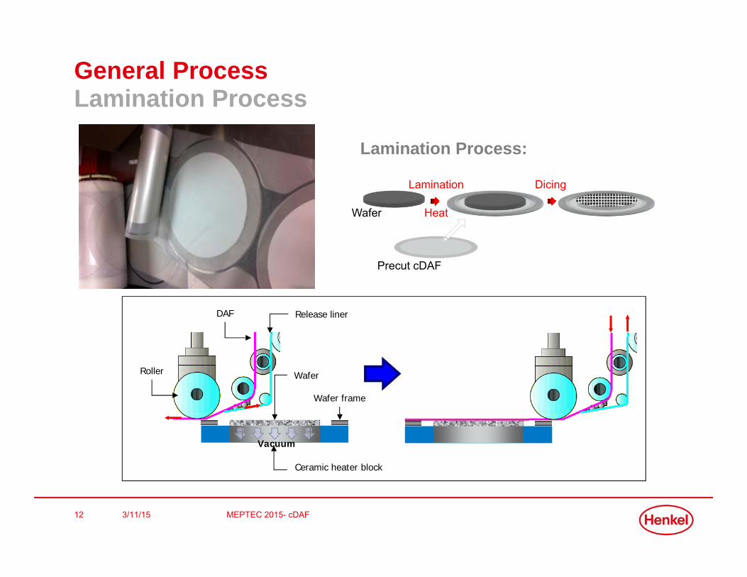
General ProcessLamination Process
3/11/15 MEPTEC 2015- cDAF
Wafer frame
Wafer
Ceramic heater block
DAF Release liner
Roller
Vacuum
Precut cDAF
Lamination Dicing
Heat
Lamination Process:
Wafer
13
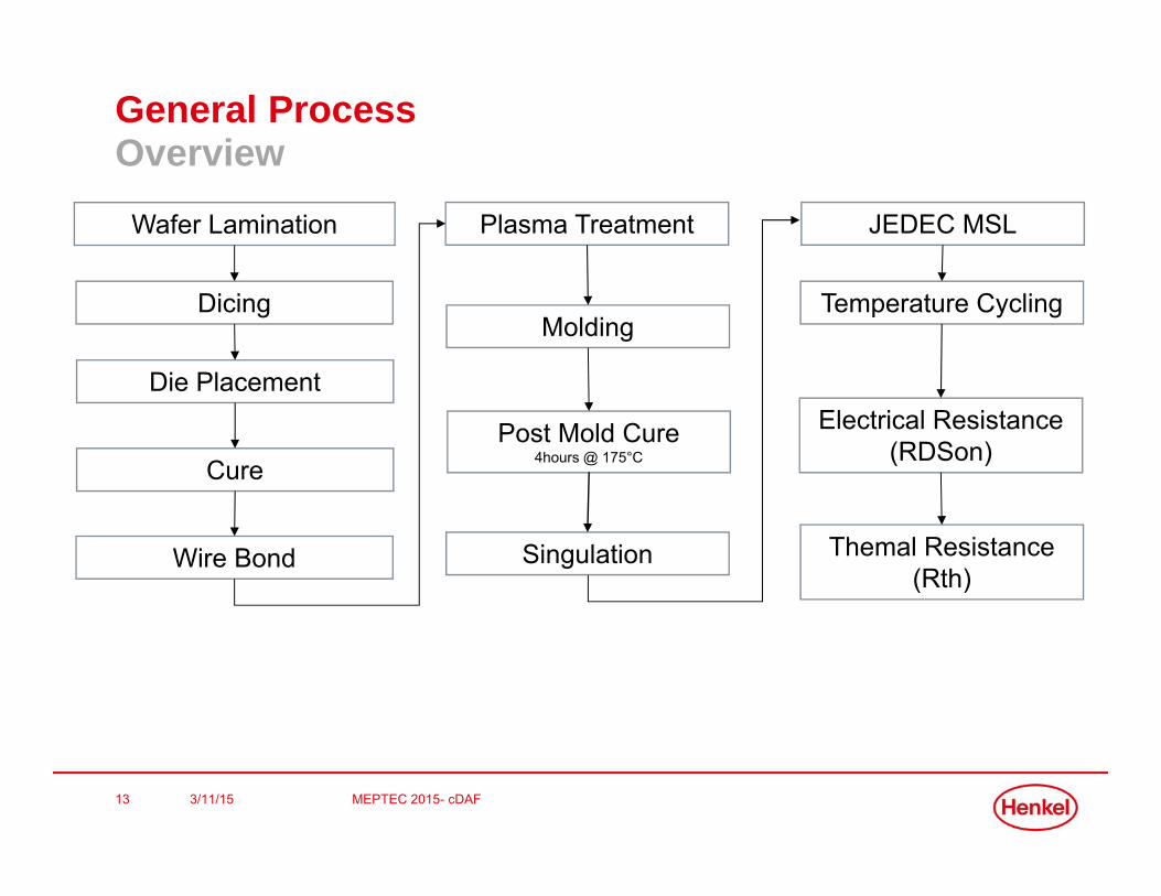
General ProcessOverview
Die Placement
Cure
Plasma Treatment
Molding
Singulation
Post Mold Cure4hours @ 175°C
Wafer Lamination
Wire Bond
JEDEC MSL
Temperature Cycling
Themal Resistance (Rth)
Dicing
Electrical Resistance (RDSon)
MEPTEC 2015- cDAF3/11/15

14
Product PortfolioProduct Space
MEPTEC 2015- cDAF3/11/15
Hig
her E
lect
rical
(Low
er R
DS
on) a
ndTh
erm
al (L
ower
Rth
) per
form
ance
Die Size
MSL1 on all LF finish
MSL2 on all LF finish
MSL2 on Laminates
2mmx2mm 4mmx4mm 6mmx6mm 8mmx8mm
CDF 300P CDF 600P
CDF 200P CDF 500P CDF 500P
CDF 800P A4: Low warpage, High thermal
A6: Sintering Film: Pb free soln

15
High Reliability Die Attach SolutionPotential for Zero Delam Applications
• Conductive films do not bleed and do not have a fillet, so the adhesion of MC to LF is stronger – regardless of LF finish: smooth or rough.
• CDAF also has minimal out-gassing, which ensures clean WB bond pads & die top –
• wirebonding or MC-die top delamination not observed
PasteRough Substrate
BleedMC
No Bleed
CDF 215PRough Substrate
MC
MEPTEC 2015- cDAF3/11/15

16
High Reliability Die Attach SolutionTest Vehicle Information
QFNsAsymmetrical package and
rigid body cause additional die
stress
• QFN12x12 PPF packages• 8x8x0.3mm dies, Au backed• DA: 130’C, 2kg, 1.5s• Cure: 30 min. Ramp + 60 min. at 200’C• Single layer 1.6 mm thick FR4 Board with 2 layers of Copper (for added rigidity)
• No electrical connections on board
• Henkel INNOLOTLF721AGS88.5V WGU 400gUS• Sn/Ag3.7/Cu0.7/Sb1.5/Bi3.0/Ni0.15, no clean solder paste
3/11/15 MEPTEC 2015- cDAF
17
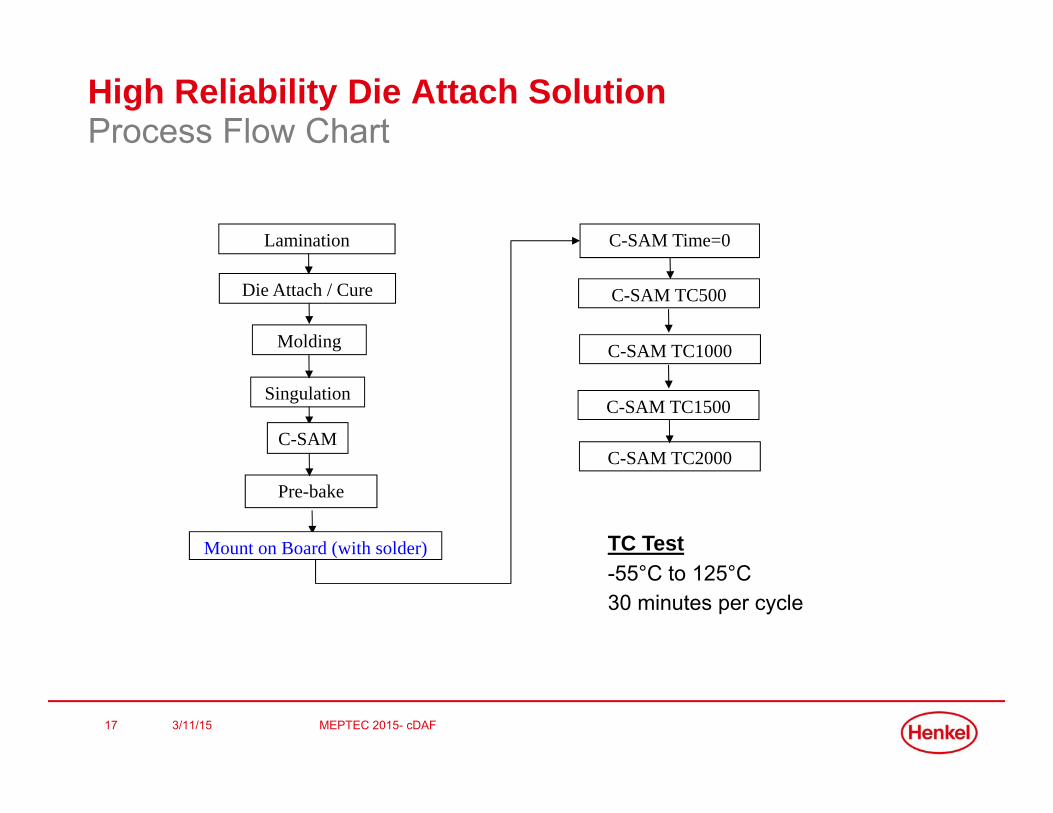
High Reliability Die Attach SolutionProcess Flow Chart
TC Test-55°C to 125°C30 minutes per cycle
Mount on Board (with solder)
C-SAM
Pre-bake
C-SAM Time=0
Singulation
C-SAM TC500
C-SAM TC1000
C-SAM TC1500
Molding
Die Attach / Cure
Lamination
3/11/15 MEPTEC 2015- cDAF
C-SAM TC2000

18
High Reliability SolutionResult Overview
No Delam.
Some Die Attach Delam.
Severe Die Attach Delam.
Material C115 CDF 515PThickness 15 um 15 um
Time 0, Before Mounting on BoardTime 0, After Mounting on Board
TC500TC1000TC1500 MC delam, no DA delamTC2000 MC delam, no DA delam
3/11/15 MEPTEC 2015- cDAF

19
High Reliability SolutionC115 Board Level TCT
Time 0 TC500 TC1000 TC1500 TC2000
Parts begin to show severe delamination at TC1000.
Die Attach Delam after TC1000
Center delam
Time 0 Wetting
Variation in wetting
3/11/15 MEPTEC 2015- cDAF

20
High Reliability SolutionCDF 515P Board Level TCT
Time 0 TC500 TC1000 TC1500 TC2000
Parts begin to show package delamination at TC1500, but no die attach delamination up to TC2000
Time 0 Wetting
No delam
Package Delam after TC1500
No delam Package delam
3/11/15 MEPTEC 2015- cDAF
21
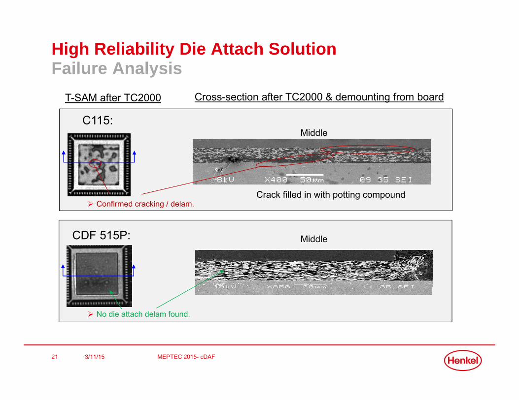
High Reliability Die Attach SolutionFailure Analysis
3/11/15 MEPTEC 2015- cDAF
C115:Middle
Crack filled in with potting compound Confirmed cracking / delam.
T-SAM after TC2000 Cross-section after TC2000 & demounting from board
No die attach delam found.
CDF 515P: Middle

22
C115 515P Note@ -65°C 14300 13670@ 25°C 10710 7590@ 150°C 3960 530@ 200°C 2820 410@ 250°C 2030 360
Warpage (um) 200°C Cure 75 54CTE (alpha1) below Tg, post cure 45 60CTE (alpha2) above Tg, post cure 120 245Tg by TMA (°C) 40 10
HDSS (kg/mm2) 260°C on 2x2mm PPF 1.3 1.1 Adhesion does not significantly differ
MSL Level Capability 2 1
MSL capability may be a parameter to practically demonstrate the DA film adhesion
TC2000 Result Change recordedSevere DA failure
Only Package failure
Modulus (Mpa)
CTE by TMA (ppm/°C)
Materials do not significantly differ
Lower modulus helps to reduce
stress during testing, as
reflected in unmolded warpage
HDSS Strength is comparatively similar between formulations
Lowering modulus is key factor to improve TC performance
High Reliability SolutionMaterial Properties
3/11/15 MEPTEC 2015- cDAF

23
3mmx3mm MSL1 5mmx5mm MSL1 8mmx8mm MSL2 9mmx9mm MSL2
CDF 515P die size range is up to 5x5mm² for MSL1 and up to 9x9mm² for MSL2.
Time 0
MSL
High Reliability SolutionCDF 515P Die Size Range
3/11/15 MEPTEC 2015- cDAF

24
High Reliability SolutionCDF 515P Compatibility with Various Leadframe Surfaces
PPF Surface Ag Spot Surface Cu Surface
CDF 515 is compatible with various leadframe surfaces and passed MSL2.
Time 0
MSL 2
Note: Die size 8x8mm
3/11/15 MEPTEC 2015- cDAF

25
High Reliability SolutionCDF 515P Compatibility with Various Wafer Back Surfaces
Wafer back: TiNiAg Wafer back: Au Wafer back: Si
CDF 515P is compatible with various wafer back surfaces and passed MSL 2.
Time 0
MSL 2Note: Die size 8x8mm
3/11/15 MEPTEC 2015- cDAF

26
SummaryThin wafer handling with precut format• Excellent electrical conductivity, very low RDSon shift (<10%)• Thinner package and smaller footprint (higher density packaging)• Potentially eliminate wafer backside metallization• In multi-die packages allow shorter die-to-die wirebonds for faster speeds.Consistent bondline thickness and controlled flow• No die tilt, • Design flexibility from tight clearance between die and die padClean dry process• No dispensing, printing/B-staging necessary• No bleed (even on rough LFs), no fillet, uniform bondline, no kerf creepReliability performance• Higher reliability performance (MSL1) on mulitiple substrates (PPF, Ag Spot, Cu) and various wafer
back metallization (Si, Au, Ag) • Achieve better efficiency, reduce yield loss: Efficient and robust process• Robust board-level temperature cycling performance for automotive application Cost Savings• Higher density leadframes, shorter Au wires and less mold compound usage
3/11/15 MEPTEC 2015- cDAF

Thank you!Thank you!

28
Appendix
MEPTEC 2015- cDAF3/11/15
29
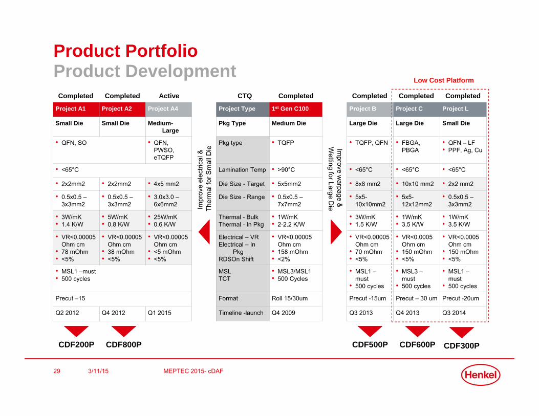
Product PortfolioProduct Development
Project A1 Project A2 Project A4 Project Type 1st Gen C100 Project B Project C Project L
Small Die Small Die Medium-Large
Pkg Type Medium Die Large Die Large Die Small Die
• QFN, SO • QFN, PWSO, eTQFP
Pkg type • TQFP • TQFP, QFN • FBGA, PBGA
• QFN – LF• PPF, Ag, Cu
• <65°C Lamination Temp • >90°C • <65°C • <65°C • <65°C
• 2x2mm2 • 2x2mm2 • 4x5 mm2 Die Size - Target • 5x5mm2 • 8x8 mm2 • 10x10 mm2 • 2x2 mm2
• 0.5x0.5 –3x3mm2
• 0.5x0.5 –3x3mm2
• 3.0x3.0 –6x6mm2
Die Size - Range • 0.5x0.5 –7x7mm2
• 5x5-10x10mm2
• 5x5-12x12mm2
• 0.5x0.5 –3x3mm2
• 3W/mK• 1.4 K/W
• 5W/mK• 0.8 K/W
• 25W/mK• 0.6 K/W
Thermal - BulkThermal - In Pkg
• 1W/mK• 2-2.2 K/W
• 3W/mK• 1.5 K/W
• 1W/mK• 3.5 K/W
• 1W/mK• 3.5 K/W
• VR<0.00005 Ohm cm
• 78 mOhm• <5%
• VR<0.00005 Ohm cm
• 38 mOhm• <5%
• VR<0.00005 Ohm cm
• <5 mOhm• <5%
Electrical – VRElectrical – In
PkgRDSOn Shift
• VR<0.00005 Ohm cm
• 158 mOhm• <2%
• VR<0.00005 Ohm cm
• 70 mOhm• <5%
• VR<0.0005 Ohm cm
• 150 mOhm• <5%
• VR<0.0005 Ohm cm
• 150 mOhm• <5%
• MSL1 –must• 500 cycles
MSLTCT
• MSL3/MSL1• 500 Cycles
• MSL1 –must
• 500 cycles
• MSL3 –must
• 500 cycles
• MSL1 –must
• 500 cycles
Precut –15 Format Roll 15/30um Precut -15um Precut – 30 um Precut -20um
Q2 2012 Q4 2012 Q1 2015 Timeline -launch Q4 2009 Q3 2013 Q4 2013 Q3 2014
Improve w
arpage &
Wetting for Large D
ieImpr
ove
elec
trica
l &
Ther
mal
for S
mal
l Die
Completed Completed Active CTQ Completed Completed Completed Completed
CDF200P CDF800P
Low Cost Platform
CDF500P CDF600P CDF300P
MEPTEC 2015- cDAF3/11/15
30
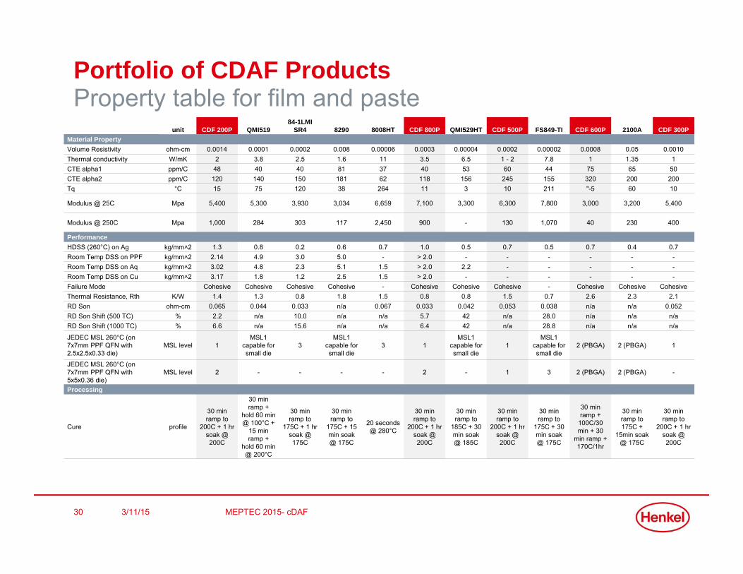
Portfolio of CDAF ProductsProperty table for film and paste
unit CDF 200P QMI51984-1LMI
SR4 8290 8008HT CDF 800P QMI529HT CDF 500P FS849-TI CDF 600P 2100A CDF 300PMaterial PropertyVolume Resistivity ohm-cm 0.0014 0.0001 0.0002 0.008 0.00006 0.0003 0.00004 0.0002 0.00002 0.0008 0.05 0.0010Thermal conductivity W/mK 2 3.8 2.5 1.6 11 3.5 6.5 1 - 2 7.8 1 1.35 1CTE alpha1 ppm/C 48 40 40 81 37 40 53 60 44 75 65 50CTE alpha2 ppm/C 120 140 150 181 62 118 156 245 155 320 200 200Tq °C 15 75 120 38 264 11 3 10 211 "-5 60 10
Modulus @ 25C Mpa 5,400 5,300 3,930 3,034 6,659 7,100 3,300 6,300 7,800 3,000 3,200 5,400
Modulus @ 250C Mpa 1,000 284 303 117 2,450 900 - 130 1,070 40 230 400
PerformanceHDSS (260°C) on Ag kg/mm˄2 1.3 0.8 0.2 0.6 0.7 1.0 0.5 0.7 0.5 0.7 0.4 0.7Room Temp DSS on PPF kg/mm˄2 2.14 4.9 3.0 5.0 - > 2.0 - - - - - -Room Temp DSS on Aq kg/mm˄2 3.02 4.8 2.3 5.1 1.5 > 2.0 2.2 - - - - -Room Temp DSS on Cu kg/mm˄2 3.17 1.8 1.2 2.5 1.5 > 2.0 - - - - - -Failure Mode Cohesive Cohesive Cohesive Cohesive - Cohesive Cohesive Cohesive - Cohesive Cohesive CohesiveThermal Resistance, Rth K/W 1.4 1.3 0.8 1.8 1.5 0.8 0.8 1.5 0.7 2.6 2.3 2.1RD Son ohm-cm 0.065 0.044 0.033 n/a 0.067 0.033 0.042 0.053 0.038 n/a n/a 0.052RD Son Shift (500 TC) % 2.2 n/a 10.0 n/a n/a 5.7 42 n/a 28.0 n/a n/a n/aRD Son Shift (1000 TC) % 6.6 n/a 15.6 n/a n/a 6.4 42 n/a 28.8 n/a n/a n/a
JEDEC MSL 260°C (on 7x7mm PPF QFN with 2.5x2.5x0.33 die)
MSL level 1MSL1
capable for small die
3MSL1
capable for small die
3 1MSL1
capable for small die
1MSL1
capable for small die
2 (PBGA) 2 (PBGA) 1
JEDEC MSL 260°C (on 7x7mm PPF QFN with 5x5x0.36 die)
MSL level 2 - - - - 2 - 1 3 2 (PBGA) 2 (PBGA) -
Processing
Cure profile
30 min ramp to
200C + 1 hr soak @ 200C
30 min ramp +
hold 60 min @ 100°C +
15 min ramp +
hold 60 min @ 200°C
30 min ramp to
175C + 1 hr soak @ 175C
30 min ramp to
175C + 15 min soak @ 175C
20 seconds @ 280°C
30 min ramp to
200C + 1 hr soak @ 200C
30 min ramp to
185C + 30 min soak @ 185C
30 min ramp to
200C + 1 hr soak @ 200C
30 min ramp to
175C + 30 min soak @ 175C
30 min ramp +
100C/30 min + 30
min ramp + 170C/1hr
30 min ramp to 175C +
15min soak @ 175C
30 min ramp to
200C + 1 hr soak @ 200C
MEPTEC 2015- cDAF3/11/15
31
Global ContactsCDAF
• Shashi Gupta – MDM• Hoon Jung – GPM
• Regional Technical Service- Kazuyasu Tanaka – Japan- Subong Yang – Korea- Leo Cheng – China- Enrico Guevarra – SEA- Solomon Wu – Taiwan- Tony Winster – EMEA- Howard Yun/Mina Chow-Taing - America
3/11/15 MEPTEC 2015- cDAF