meptec report winter 2013
DESCRIPTION
A Quarterly Publication of the Microelectronics Packaging and Test Engineering CouncilTRANSCRIPT
A Quarterly Publication of The Microelectronics Packaging & Test Engineering Council Volume 17, Number 4
SPRING 2011 MEPTEC Report 3
-INSIDE THIS ISSUE
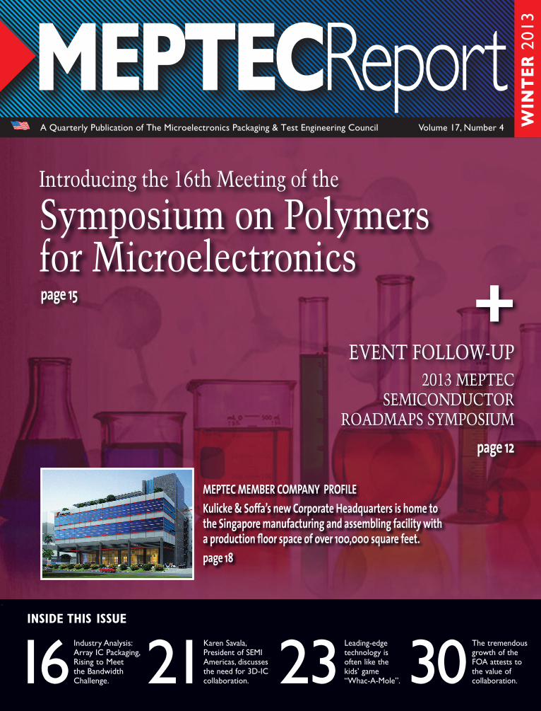
16 Industry Analysis: Array IC Packaging, Rising to Meet the Bandwidth Challenge. 21
Karen Savala, President of SEMI Americas, discusses the need for 3D-IC collaboration. 23
Leading-edge technology is often like the kids’ game “Whac-A-Mole”. 30
The tremendous growth of the FOA attests to the value of collaboration.
WIN
TER
201
3
MEPTEC MEMBER COMPANY PROFILEKulicke & Soffa’s new Corporate Headquarters is home to the Singapore manufacturing and assembling facility with a production floor space of over 100,000 square feet.page 18
Introducing the 16th Meeting of the
Symposium on Polymersfor Microelectronics page 15 +
EVENT FOLLOW-UP2013 MEPTEC
SEMICONDUCTORROADMAPS SYMPOSIUM
page 12
C
M
Y
CM
MY
CY
CMY
K
ASE_AD_8x10.5in_05102013.pdf 1 13/5/10 下午7:23
I WAS LISTENING TO AN INDUSTRY presentation recently, where the presenter mentioned that the growth in the semicon-ductor industry for 2014 would be around 5%, and this would be “good growth”. In reality, it was only about five to six years ago that our industry diverted from our previous 15% average expected annual growth, and conceded to the reality of a 7% annual growth rate. Over the last three years following the recovery year in 2010, according to Gartner data, we have seen semiconductor market growth of 2.1% for 2011, -2.6% for 2012, and pro-jected 5.2% for 2013 (but will likely be revised downward). The projected growth this year is almost entirely due to DRAM and Flash pricing increases, attributed to general DRAM industry consolidation, and then exacerbated by an early Septem-ber fire in a Hynix DRAM fab in Wuxi, China taking significant manufacturing capacity off line. Over the past three years, the semi-conductor industry has grown slower than worldwide GDP. I guess our indus-try is not reaping the rewards of the high GDP growth in China and India, which is not very surprising. So what is the out-look for IC packaging? Will we just fol-low the trend for semiconductor growth? Will it be better or worse? Where are the opportunities? The industry is consolidating, that’s one thing for sure. Many companies have exited businesses that were their main-stay only a few years before. The once dominant PC industry is taking huge pressure from alternative devices such as tablets. But, there are opportunities for growth. From an application standpoint, smartphones and tablets are driving the bulk of the industry growth with very diverse requirements, rich in digital, ana-log, memory, and MEMS content. Does IC packaging have a value prop-
shorter and shorter product lives.
Millimeters, Microns, and Nanometers Another trend, driven by the minia-turization requirements of mobile and handheld devices, is volumetric size reduction of systems and the components that power them. Until today, IC’s are fabbed with nanometer (or submicron at least) transistors and interconnect on the silicon. IC packages are becoming finer and finer pitch at the interconnect level, with flip chip pitches going below 150 microns, in some applications to below 50 microns. Wirebond has capability to bond down to 40 micron bond pad pitch, and is still reducing. The pitch of the interconnect on the package is now going below 0.5mm, down to 400 or even 300 microns as the motherboard technology inside these mobile devices migrates lower. So what about the millimeters? This is the domain of solder interconnect, of the contract manufacturing business, but this trend is also pushing all but the most capable CM’s beyond their readily available abilities to handle these finer and finer pitch devices in smaller and smaller form factors, including many in bare die packages such as WLCSP.
System Integrators Traditionally, system OEM’s would architect their system by taking available technologies from their semiconductor suppliers and partners. As growth has started to wane, semiconductor compa-nies have obtained broader capabilities through acquisition or internal develop-ment to provide more coverage of the system or sub-system BOM (bill of materials), integrating more functions into their products, and thus providing more value. We are starting to see system
osition in this new era? Or will IC pack-aging value, and thus profitability, wane as the industry further consolidates? Let’s consider a couple more aspects to the puzzle.
Impact of Moore’s Law The financial formula for continu-ing Moore’s Law is becoming more and more difficult to manage. The expenseof wafer fab facilities and equipment is
something only a handful of manufactur-ing companies can bear. The cost of mask sets, as well as design environments and resources is beyond what only a small number of fabless or even IDM compa-nies can justify, and only for their high-est volume products. The difficulty of migrating IP to new nodes, especially in analog, is making companies think about partitioning their product architecture in ways they didn’t expect a few years back. Bottom line, even though some companies will continue their march to utilize deep submicron fab capabilities in the future, the industry as a whole will not necessarily benefit from Moore’s Law any more. There must be other ways found to offer the functions needed in cost effective ways without spending nine, ten or eleven figures in USD to launch semiconductor products that have
BOARD LETTER
Industry Perspectives and the Future of IC PackagingRich Rice Senior Vice President of SalesASE (U.S.) Inc.MEPTEC Advisory Board Member
WINTER 2013 MEPTEC REPORT 3meptec.org
I am bullish about the future of packaging. I believe if players
are positioned well, thanks to the ever increasing cost of
Moore’s Law, packaging opportunities are alive and
well for the foreseeable future, especially in the SiP arena.
continued on page 29
MEPTEC Report Vol. 17, No. 4. Published quarterly by MEPCOM LLC, P. O. Box 222, Medicine Park, OK 73557. Copyright 2013 by MEPTEC/MEPCOM LLC. All rights reserved. Materials may not be reproduced in whole or in part without written permission. MEPTEC Report is sent without charge to members of MEPTEC. For non-members, yearly subscriptions are available for $75 in the United States, $80US in Canada and Mexico, and $95US elsewhere. For advertising rates and information contact Gina Edwards at 408-858-5493, Fax Toll Free 1-866-424-0130.
A Quarterly Publication of The Microelectronics Packaging & Test Engineering Council Volume 17, Number 4
The MEPTEC Report is a Publication of the Microelectronics Packaging & Test
Engineering Council
P. O. Box 222, Medicine Park, OK 73557Tel: (650) 714-1570 Email: [email protected]
Publisher MEPCOM LLC
Editor Bette Cooper
Art Director/Designer Gary Brown
Sales Manager Gina Edwards
MEPTEC Advisory Board
Board Members
Ivor Barber Xilinx, Inc.
Jeanne Beacham Delphon Industries
Joel Camarda Amonix, Inc.
Jeff Demmin STATS ChipPAC, Inc.
Douglass Dixon Henkel Corporation
Farshad Ghahghahi LSI Corporation
Nikhil Kelkar Exar Corporation
Nick Leonardi Premier Semiconductor Services
Phil Marcoux PPM Associates
Bhavesh Muni Dow Chemical Corp.
Kumar Nagarajan Maxim Integrated
Raj Pendse STATS ChipPAC
Rich Rice ASE (US) Inc.
Jim Walker Gartner
John Xie Altera Corporation
Special Advisors
Bance Hom Consultech International, Inc.
Ron Jones N-Able Group International
Mary Olsson Gary Smith EDA
Mike Pinelis MEMS Journal, Inc.
Honorary Advisors
Seth Alavi Sunsil
Gary Catlin Plexus
Rob Cole
Skip Fehr
Anna Gualtieri Elle Technology
Marc Papageorge Semiconductor Outsourcing
Contributors
Joe Ardini Fab Owners Association
Kevin Becker Henkel Electronic Materials, LLC
Ira Feldman Feldman Engineering Corp.
Ron Jones N-Able Group International
Ron Leckie INFRASTRUCTURE Advisors
Herb Reiter eda 2 asic Consulting
Rich Rice ASE (U.S.) Inc.
Karen Savala SEMI Americas
Paul Werbaneth 3D InCites
Sandra Winkler New Venture Research
WIN
TE
R 2
013
ON THE COVERMEPTEC is pleased to announce they have been asked to organize the 16th Meeting of the Symposium on Polymers for Microelectronics. The charter of the symposium is to promote the study of the integration of polyimides and other advanced polymeric materials into semiconductor, thin film packaging, MEMS and optical application areas. It is being held on May 6-8 at the beautiful Winterthur Gardens in Wilmington, Delaware. See page 15 for more information.
16 ANALYSIS – YouTube, Facebook, Twitter, smart phone apps, and many other Internet uses are driving up the
bandwidth requirements from our electronic devices. This is demanding more and more of the electronics within the electronic gadget, including the IC package which connects the IC to the board and the other chips.
BY SANDRA WINKLERNEW VENTURE RESEARCH
21 STANDARDS – Standards work at JEDEC and SEMI are contributing to the market’s development, both to
enable processes and cost-reduce manufacturing, but without the emergence of a new, robust collaboration model that can deliver meaningful agreements between key constituencies, the promise of 3D innovation will remain distant and illusive.
BY KAREN SAVALA SEMI AMERICAS
18 PROFILE – As a pioneer in the industry, Kulike & Soffa has provided customers with market leading packaging
solutions for decades. In recent years, K&S has expanded its product offerings through strategic acquisitions, adding wedge bonding and a broader range of expendable tools to its core ball bonding products.
KULICKE & SOFFA MEMBER COMPANY PROFILE
DEPARTMENTS 3 Board Letter 5 Member News
8 Industry Insights Column 10 Coupling & Crosstalk Column 12 Event Follow-Up
26 Henkel News30 Opinion
14 MEPTEC REPORT WINTER 2013 meptec.org WINTER 2013 MEPTEC REPORT 15meptec.org
ANALYSIS
Array IC Packaging, Rising to Meet the Bandwidth Challenge Sandra Winkler, Senior Industry Analyst New Venture Research
YOUTUBE, FACEBOOK, TWITTER, smart phone apps, and so many other Internet uses are driving up the band-width requirements from our electronic devices at a tremendous pace. Sharing photos now a days does not involve passing around a photo album in the liv-ing room. Today photos and videos are shared electronically nearly the instant they are taken as they are loaded up on Facebook and other social media, often from small handheld electronic gadgets such as tablets and smart phones. Smart phones are also changing the way we do business. Small businesses away from electrical outlets can check competitor pricing on goods being sold even in third world countries and charge a sale using an attached Square device. Medical doctors can now add an attach-ment to their smart phones to help with diagnosis of medical problems, which has the potential to revolutionize the medical industry into the portable realm. This will not only reduce medical costs, but will also expand medical coverage into areas of the world which otherwise would not reap the benefits of modern medicine. This use of the Internet is demanding more and more of the electronics within the electronic gadget, including the IC package which connects the IC to the board and the other chips. Small size, high performance, lower power require-ments, and reduced battery usage are all hot button issues which are influenced more and more by IC packaging. Array IC packaging, in which the package I/O are beneath the package in an array layout rather than just at the perimeter as with traditional leadframe packages, allow for the higher density needed to meet those issues in order to keep pace with the advancing speed of the IC device and demand for bandwidth capability.
The IC package is the determining factor in the following:• Footprint or space consumed on the printed circuit board (PCB).• Physical length and thus speed it takes for the electron to leave the IC to travel to other ICs and the PCB.• Influences the battery usage and power requirements. Array packages include the PGA, BGA, FBGA, Fan-in QFN, and Fan-out and Fan-in WLPs. The pin grid array, or PGA, is a through-hole package with pins which attach it to the PCB. The other packages have more options.
BGA / FBGA BGAs and FBGAs do not have to have solder balls beneath the package substrate; the package can have just land pads or columns instead of balls for the second level interconnection, which con-nects the package to the printed circuit board. In the absence of solder balls, where land pads form the connection to the PCB, the package is considered to be a land grid array (LGA). If the initial form factor is in the fine-pitch, close to die size category, as it is with the FBGA, the land package is a FLGA. These land packages are shorter in
Figure 1. BGA / LGA / CGR Units, 2012 vs. 2017.
2012 2017
CGA, 0.6%LGA, 11.5%
BGA, 87.9%
CGA, 0.6%LGA, 10.4%
BGA, 89.0%
the “z” dimension, making them ideal in ultra-thin products where the over-head space for a package is at a mini-mum. However, in the absence of the self-centering nature of the solder balls, package placement on the PCB must be more accurate, thus more expensive with slower throughput than their balled coun-terparts. Packages with column attachment to the PCB are known as column grid arrays (CGAs), which allow for a finer pitch than solder balls, and more inter-connection density. These are more expensive to produce than the BGA or LGA package solutions. Figure 1 illustrates the percentage breakout for the years 2012 versus 2017 for the BGA / LGA / CGA package solu-tions. The same information is provided for the total FBGA package family in Figure 2.
Fan-In QFN Package Solutions The quad flatpack no-lead, or QFN, is a newer package introduced onto the market in 2008. It was designed to reach into markets with a lower I/O count than the larger I/O count QFP, and capture the lower end of that market. It is close to die size, thus considered a chip scale package, or CSP. A new twist has been added to the QFN to add additional rows to this leadframe package, turning it into a leadframe version of an array package, and one that can reach even further into the market which would otherwise be covered by the larger QFP. Additional rows are “fanned in” from the traditional perimeter-style leadframe, making this package unique. Two to three rows of leads are cre-ated to form a perimeter array pattern on the underside of the package. The leadframe is stamped or etched as in any other leadframe solution, but the leads are of various lengths, either two or three different lengths. When bent downward for connection to the PCB by trim and form equipment, the result is a multi-row, array-patterned package solution with a hole in the center, or fan-in QFN. This allows the number of package leads to extend into the hundreds, up from generally fewer than 50. The resulting package is a high-density, leadframe array package.
Like the Fan-in QFN, demand for both the WLP and the Fan-out WLP are on the rise, shown in Table 2.
Total Array IC Packaging The total of the array packages, including PGA, BGA, FBGA, Fan-in QFN, and Fan-out and Fan-in WLPs, was 27.5 percent of the total IC packages (less DCA and accounts for multi-die packages) assembled in 2012. The com-pound annual growth rate (GAGR) of ICs is 5.5 percent for the years through 2017. With this expanding number of ICs being produced each year, the percent of array IC packages being assembled will increase to 29 percent in 2017, thus they are growing at a faster rate than perim-eter outline packages.
More Information More information on these package solutions can be found in New Venture Research’s newly published report, Array IC Packaging Market. To find out more about this and other reports on IC pack-aging, please contact Karen Williams at [email protected], Tel: 1-(408) 244-1100, or Sandra Winkler at [email protected], Tel: 1-(650) 299-9365. See newven-tureresearch.com for information on all the reports from NVR. ◆
Demand for both the traditional QFN and Fan-in QFNs are on the rise, see in Table 1.
Fan-Out WLPs Wafer Level Packages, or WLPs, are the smallest package solution on the mar-ket, being die sized. This unique package is formed while the die are still part of an uncut wafer, the only package to be created or assembled in this manner. All the solder balls or bumps then must fit beneath the die itself, which limits the number of I/O which is on these pack-ages. Reconfigured or Fan-out wafer-level packages were introduced in 2006. After devices are manufactured on a wafer, the devices are sawn and transferred on a carrier to another larger wafer that has gaps between die, which are filled with overmold material that also coats the back side of the devices for protec-tion, enlarging the “face” of the die. This allows for a larger surface on which to extend a redistribution layer (RDL), thus allowing for far more I/Os than would be possible on the original smaller surface. Solder balls or bumps can be added to this surface for interconnection to a print-ed circuit board. All these processes are done on an uncut wafer, so that manufac-turing efficiencies are maximized.
2012 2013 2014 2015 2016 2017
QFN Percentage of Total IC Packages 12.4% 12.7% 13.2% 13.8% 14.4% 14.8%
Growth Rate of Fan-In QFN and QFP 184.5% 15.4% 25.9% 11.9% 10.5% 9.9%
As a Percentage of Total QFN Market 3.4% 3.6% 4.1% 4.2% 4.3% 4.3%
Table 1. Fan-In QFN
2012 2013 2014 2015 2016 2017
WLP Percent of WW IC Packaging Mkt 5.3% 5.5% 5.7% 5.9% 6.0% 6.1%
Growth Rate for Fan-out WLPs 60.1% 19.0% 17.0% 16.6% 6.8% 6.1%
Fan-out WLP Percent of total WLPs 9.5% 10.1% 10.8% 11.5% 11.7% 11.6%
Table 2. Fan-Out WLP
Figure 2. FBGA / FLGA Units, 2012 vs. 2017.
2012 2017
FLGA, 20.8%
FBGA, 79.2%
FLGA, 20.1%
FBGA, 79.9%
MATERIALS
The Lead-Free “Whac-A-Mole”
die and the thickness of the packages so that multiple die can be stacked in a sin-gle package (3D packaging) and multiple packages can be stacked on top of each other (POP, or Package-On-Package). Additionally, the electrical com-plexity has also been escalating due to Moore’s Law, so to handle more and faster signals with more power in this smaller space, it requires the use of com-plex multi-layer laminates with metal patterns embedded within insulating materials such as resins. Of course, the various materials including silicon, met-als and inorganic resins all have differing Coefficient of Thermal Expansion (CTE) so, when subjected to heat, this induces stress between the layers and can cause warpage. The direction and magnitude of the warpage is the result of complex vari-ables including the number of metal lay-ers in the board and their design layout. While much of this is evolutionary and “business as normal” in the electron-
directly soldered to the corresponding pads on the package substrate. Similarly, package-to-PCB connection has migrated to a direct (no-lead or lead-less) surface mount where flexible package leads are replaced by small solder balls or paste arrayed in a pattern across the base of the package – hence the term Ball Grid Array (BGA) package. These BGA pack-ages are then mounted to corresponding patterns on PCBs by mounting them in position and reflowing the solder balls to make direct electrical connection between the chip’s package and board. The resulting direct chip-to-package and direct package-to-board connections clearly now have much less flexibility to be able to withstand non-flatness or warpage in the surfaces that must come and stay together robustly for the end product to work. The continuing minia-turization of electronics has also driven chipmakers to drastically reduce the thickness (really thinness) of the silicon
LEADING-EDGE TECHNOLOGY is often like the favorite kids’ game, “Whac-A-Mole”, in that when one prob-lem is solved, another often pops up in a different area. In our haste to solve one problem, we may have created another. One example we will discuss here is the drive over the last several years to convert to lead-free materials and manufacturing. While the motivation and pressures to expunge tin-lead solder are definitely well-intended and undoubtedly the right thing to do, they have worked with some other trends to exacerbate problems associated with substrate and board warpage.
Background To put things in perspective, let’s reflect back in time to consider the con-tinuing evolution of electronics minia-turization. Silicon die were packaged for many years by bonding them base-down on a package lead-frame or substrate. Then electrical wire bond connections were made from the pads on the die sur-face to corresponding pads on the frame or substrate before being encapsulated with plastic or some form of sealed lid. The internal connections were in turn routed out of the package via metal leads, which the customer would then solder to printed circuit boards (PCBs). While the die needed to be in relatively flat contact with the package to be bonded and the package needed to be relatively flat to the PCB, there was more than sufficient flexibility in the wire bonds and package leads to take up any slack caused by non-flat surfaces, flexing or thermal expan-sion mismatch. Driven over the past several years primarily by the needs of the hand-held electronics community, the die-to-package connection has been migrating more to flip-chip where the top surface of the chip or die is flipped face-down on the package base and metal bumps are
Ron Leckie, President, INFRASTRUCTURE AdvisorsPartner, Ackrell Capital, Board of Directors Member, Delphon Industries, LLC Founding Member of the GlobalScot Network
The Package-to-PCB Interface. Image courtesy of Akrometrix
Standards Momentum built across the micro-electronics manufacturing community with papers on the problem being pub-lished by large companies such as Alca-tel, Altera, Blackberry, Celestica, Delphi, Ericsson, Flextronics, Infineon, Intel, Micron, Sanmina, etc. The challenge in the fragmented supply chain was that without a common methodology to mea-sure warpage, it was too easy to “point fingers” upstream or downstream while the failure mechanisms persisted. The initial challenge was in identifying stan-dardized practical methods for measuring and quantifying warpage. The resulting standards that have been published include JEITA’s (Japan Electronics & IT Association) warpage specification; iNEMI’s (International Electronics Manufacturing Initiative) Package Qualification Criteria and Road-map; JEDEC’s (formerly Joint Electron Device Engineering Council) standards that apply to measuring warpage for chip packages at temperature; and more recently, the IPC (originated as Institute for Printed Circuits) standard for board warpage. The process to obtain agree-ment on standards can be lengthy and difficult, but the fact that this recent IPC standard was developed in a year, and passed with approval on its first ballot, is a strong testament to the industry’s support and commitment to finding solu-tions.
Solutions With the right metrology in place to characterize a given application, it is then possible to make refinements
tive or even have no electrical contact. In either case, this represents a failure mechanism either at test or over time in the field. The transition to lead-free sol-der uses different materials and requires higher reflow temperature profiles which aggravate the warpage.
Surfacing The Problem As the market forces driving minia-turization resulted in increased intercon-nection challenges due to warpage, the EMS and ODM companies appeared to “keep the lid” on the problem by cre-atively tweaking the solder reflow pro-cess to accommodate the symptoms of warpage. This was achieved through such items as increased solder paste thick-ness or wider mask openings to deposit more solder selectively at weaker areas on circuit boards. This is what talented manufacturing engineers do – change processes to maximize yields and quality. However, this warpage phenomenon was eventually surfaced as a problem by senior technologists at industry forums through technical papers on the topic. As voices became louder and it became apparent that this was a critical emerging industry problem, the various industry trade associations and standards bodies started working on it in pre-competitive forums. The result is that technology Roadmaps were developed to identify the problems and map out the need for improved flatness/warpage specifications and better design for manufacturability. As a result, standards have been devel-oped and published to describe how to measure flatness/warpage on both com-ponents and printed circuit boards.
ics industry as we strive for increased functionality and performance in smaller form factors, On top of all this, over the last decade the industry has had to convert, due to environmental concerns, to lead-free materials with lead-free solder being the operative one that has had the big-gest impact on the electronics packag-ing trends described above. Lead-free solder requires higher temperatures than traditional tin-lead solder to become mol-ten and reflow. This drives the need to change many of the materials that have been in use for decades in the manufac-ture of microelectronics components and systems. These new materials behave differently than their predecessors and, with the higher temperatures, exacerbate this warpage behavior. So, in solving the problem of removing lead, we now have increased the problems associated with warpage.
Manifestation In terms of the final assembled prod-uct, this warpage can impact it by poten-tially causing some of the electrical joints between the semiconductor package and the PCB to either not make connection (a manufacturing yield and cost impact) or make a weak connection that works ini-tially but fails over time/use (a reliability impact - and even greater cost impact). The most common symptom of warpage has been coined, “HnP” or “Head in Pillow” which has been widely documented in the industry. This failure mechanism gets its name from the shape of the deformed solder joint which is cre-ated when the board and package warp in different directions to start separating as the solder joint forms through reflow. While there are other contributing fac-tors such as misalignment, materials and thermal reflow profile, it is believed that warpage is a primary concern. Figure 1 shows an example of pack-age warpage changing over temperature from concave to convex. As the solder melts, the ball and paste are not in con-tact and reflow cannot occur before the solder surface starts to oxidize. On cool down the warpage reduces and the oxi-dized surfaces make contact but do not make a perfectly reflowed solder joint. In some cases, these will appear under visual inspection to have formed a joint but in actuality could be either resis-
Figure 1. HnP Formation. Image courtesy of Akrometrix
After BGA Placement
Tem
pera
ture
Time
component
PCB
(a)
(b)
(c)
(d)
(e)
In Soak Zone
Above SolderMelting Point
Head & PillowDefects
20 MEPTEC REPORT WINTER 2013 meptec.org WINTER 2013 MEPTEC REPORT 21meptec.org
A Quarterly Publication of The Microelectronics Packaging & Test Engineering Council Volume 17, Number 4
SPRING 2011 MEPTEC Report 3
-INSIDE THIS ISSUE
16 Indusrty Analysis: Array IC Packaging, Rising to Meet the Bandwidth Challenge. 21
Karen Savala, President of SEMI Americas, discusses the need for 3D-IC collaboration. 23
Leading-edge technology is often like the kids’ game “Whac-A-Mole”. 30
The tremendous growth of the FOA attests to the value of collaboration.
WIN
TER
201
3
MEPTEC MEMBER COMPANY PROFILEKulicke & Soffa’s new Corpoarte Headquarters is home to the Singapore manufacturing and assembling facility with a prodcution floor space of over 100,000 square feet.page 18
Introducing the 16th Meeting of the
Symposium on Polymersfor Microelectronics page 15 +
EVENT FOLLOW-UP2013 MEPTEC
SEMICONDUCTORROADMAPS SYMPOSIUM
page 12
deliver first-class customer service solu-tions. This innovative spirit and belief differentiates the company from competi-tors and influences customers around the world to embrace the K&S brand. At K&S, innovation never stops.
K&S Heritage: The Past and Present K&S was founded in 1951 and was incorporated in 1956. The company has grown to become the top global leader in the package assembly industry. The company provides equipment and tools that are used in the production of a wide range of semiconductor devices. K&S is headquartered in Singapore, where its corporate operations, engineering, manu-facturing, research & development, and sales & marketing facilities span approx-imately 198,000 square feet. The compa-ny is an ISO 9001 certified organization, and is focused on delivering high quality and reliability in both product design and customer service. The company has over 2,200 employees in 15 cities.
For more information about K&S and its products and services, visit www. kns.com. ◆
Kulicke and Al Soffa instilled a philoso-phy that is reinforced by the company’s leaders through relentless mentoring and the belief that a great innovative idea could come from anyone and anywhere within the organization. K&S remains committed to innovation in its technol-ogy and solutions that would help cus-tomers meet their needs and to overcome challenges. The company believes and continues to leverage the spirit of inno-vation and the rich history of technologi-cal breakthroughs into new solutions and drive future growth. As an extension to its belief, K&S introduced “Technology. Innovation. Solutions” in 2013 – a unified brand mes-sage that symbolizes the spirit of innova-tion. This reflects its tireless commitment to new ideas and customer feedback that inspire the company to see around
corners. K&S believes in offering more than just technology solutions and
the company aims to
K&S and the Global Marketplace K&S is able to effectively and con-tinuously market its products and ser-vices to both contract manufacturers and integrated device manufacturers for a wide range of applications through the organization’s highly driven and incred-ibly talented people. The company offers a diverse and comprehensive array of solutions that suit any potential need of customers around the globe. K&S is a customer centric organization with a proven track record of delivering innova-tive, high quality, cost effective solutions, and best-in-class services.
Technology Leadership K&S leverages on its world class diverse research and development group consisting of over 450 employees across six countries. The company continues to be the technology leader by working closely with its customers and industry-leading partners to overcome new chal-lenges. Its strategy and the core of prod-uct development are achieved through technological process advancement through innovation. The company’s core technology com-petencies can be broadly categorized as follow:
• High Speed Motion• Vision System• Ultrasonic• Packaging Development• Material Handling
Extending the K&S Product and Services Portfolio K&S introduced IConnPS ProCu PLUSTM, the world’s most advanced cop-per wire bonder that strengthens K&S’ position as a premier leader and provider of copper wire bonding solutions at the recent SEMICON Taiwan 2013 in Sep-tember. At the tradeshow, K&S also pre-sented ACS ProTM, a new generation of copper capillary that offers great opera-tion benefits for advanced copper wire bonding applications.
PROFILE
20 MEPTEC REPORT WINTER 2013 meptec.org
Earlier in the year, the company pre-sented the line of OptoTM high quality blades for LED package singulation with hub or hubless design that provide flex-ibility per dicer and process configura-tion. The customer centric company also launched K&S Care in March 2013, a professional after sales service program that is designed to help customers to operate their K&S machines at an opti-mum level.
K&S also introduced PowerFusionPSTM,
a high performance wedge bonder driven by a new powerful direct-drive motion system and expanded pattern recognition capabilities that deliver industry leading productivity and reliability.
Over 60 Years of Successful Innovation – and Counting K&S created the world’s first wire bonder and became one of the world’s first suppliers of semiconductor assembly equipment. Since its introduction, K&S has continued to develop innovative wire bonding technologies. Founders Fred
K&S OVERVIEW
Kulicke & Soffa (NASDAQ:
KLIC) is the global leader in
the design and manufacture
of semiconductor assembly
equipment. As a pioneer in
the industry, K&S has provided
customers with market lead-
ing packaging solutions for
decades. In recent years, K&S
has expanded its product
offerings through strategic
acquisitions, adding wedge
bonding and a broader range
of expendable tools to its core
ball bonding products. Com-
bined with its extensive exper-
tise in process technology,
K&S is well positioned to help
customers meet the challenges
of assembling the next-genera-
tion semiconductor devices.
ACS Pro™ Copper Capillary
Offering Industry-Leading Innovative Technology Solutions and Best-in-Class Services
The new K&S Corporate Headquarters – home to the Singapore manufac-turing and assembling facility with a production floor space of over 100,000 square feet.
IConn
PS ProCu PLUSTM
Copper Wire Bonder
PowerFusion
PSTM
High Performance Wedge Bonder
WINTER 2013 MEPTEC REPORT 21meptec.org
Opto™ Blades
23 MATERIALS – Leading-edge technology is of-ten like the kids’ game, “Whac-A-Mole”, in that
when one problem is solved, another often pops. In our haste to solve one problem, we may have created an-other. One example is the drive over the last several years to convert to lead-free materials and manufacturing.
BY RON LECKIE INFRASTRUCTURE ADVISORS
STANDARDS
Collaboration Needed on 3D-IC
was an American effort, but in 1998 the roadmap became an international pro-cess, today’s International Technology Roadmap for Semiconductors (ITRS). Today, the ITRS has expanded to address not only critical requirements to sustain Moore’s Law, but also the key develop-ment milestones necessary in the More-Than-Moore—in areas like advanced packaging and MEMS. R&D costs have also expanded to meet the targets dictated by Moore’s Law. In the early days, only the largest R&D lab in the world, Bell Labs, could manage the multi-disciplinary require-ments for semiconductor chip develop-ment. Eventually, collaborative research consortia emerged that allowed industry players to pool resources in a pre-com-
was small, semiconductor progress as defined by Moore’s Law occurred nearly simultaneously in different companies. Progress was achieved through science and technology innovation occurring through independent R&D labs and spread through academia and commercial competition. Later, as the scale, scope and complexity of semiconductor manu-facturing expanded exponentially—with much of the R&D distributed throughout the supply chain involving hundreds of equipment and materials suppliers each specializing on their unique role in the fabrication process—industry roadmaps were required to keep everyone on pace. No single firm could master all the ele-ments of innovation required for Moore Law improvements. For several years it
THE HISTORY OF SEMICONDUCTORS has been a history of collaboration. For decades, the great leaps forward in semi-conductor cost reductions and perfor-mance improvements have been achieved through widespread industry collabora-tion efforts in technology roadmaps, manufacturing standards, wafer size transitions, collaborative R&D consortia, international trade agreements, and other areas. Today, a similar industry-wide col-laborative approach to 3D stacked ICs is needed to reach widespread 3D-IC adop-tion and continue the amazing progress our industry has historically achieved. I presented on this topic at the 2013 MEPTEC Roadmaps Symposium on September 24 in Santa Clara, California. In the past, when the industry
Karen SavalaPresidentSEMI Americas
3D-IC Standards Committees
Thin Chip (Die) BendingStrength Measurement
Task Force
3D-IC Study Group
Middle End ProcessTask Force
TestingTask Force
Wafer Bonded StacksTask Force
Inspection & MetrologyTask Force
Thin Wafer HandlingTask Force
North America 3DS-ICCommittee
Taiwan 3DS-ICCommittee
Japan PackagingCommittee
SEMI International Standards, Nov. 2013
For heterogeneous integration of memory and logic, the industry still needs design tools, thermal solutions, continued work on wafer bonding and de-bonding, and accepted test methodologies, to name a few requirements. Gartner estimates that TSV adoption for memory will be pushed out to 2014 or 2015, with non-memory applications delayed to 2016-17 if that. They cur-rently forecast that TSV devices will account for less five percent of the units in the total wafer-level packaging market by 2017. For 3D-IC to be widely adopted, meaningful collaboration throughout the value chain still needs to occur. At this time in the market, all the important players in the ecosystem have a differ-ent perspective. All the players have a business model that must be defended or exploited based on what technical dis-coveries occur and what customers even-tually want. TSMC sees an integrated approach that threatens the traditional Fabless/Foundry/OSAT model. Obvi-ously leading OSATs prefer this vision as it provides an opportunity to expand their business. But OSATs themselves are looking at ways to differentiate. IDMs like Intel probably see the fabless model coming full circle with 3D IC. Fabless companies believe that 3D must emerge in ways that continue their own—and their customer’s — familiar multiple-sourcing considerations. We’ll continue to see discoveries, inventions and new products in 3D-IC and progress will continue. Hundreds of patents in the area have already been issued. We’re seeing innovation and invention in wafer bonding, via manufac-turing, and other areas. Standards work at JEDEC and SEMI will also contribute to the market’s development, both to enable processes and cost-reduce manu-facturing, but without the emergence of a new, robust collaboration model that can deliver meaningful agreements between key constituencies, the promise of 3D innovation will remain distant and illu-sive. For information on SEMI, visit www.semi.org; for information on SEMI International Standards, visit www.semi.org/en/Standards. ◆
Consortium (G450C) to manage 450mm wafer processing requirements. Recently, G450C set up a separate fab facility consortium. Europe has launched five separate 450mm projects or consortiums, with two others on the drawing board. Israel has established 450mm consortium on metrology and Japan has collaborative arrangement on 450mm with Toshiba. With uncertainties on 450 wafer processing, EUV lithography, and the continued transition to new transistor architectures, many experts are question-ing the continuation of Moore’s Law. It’s been reported that cost targets at 28 nanometers were not reached, 20 nano-meters may be delayed and also come in at a high price. Consequently, the industry has been excited about More-than-Moore applications, especially 3D stacked ICs that promise to improve bandwidth, reduce footprint, decrease power consumption, and lower cost. We have seen the proliferation of stacked die with wire bond or flip chip, stacked packages, package-on-package, and chip-on-chip packages. But today, the most anticipated innovation is 2.5 and 3D stacked ICs using TSVs to achieve both the power and bandwidth benefits associated with a radical new interconnect solution. Like 450mm wafer processing, critical standards foundation work for the adoption 3D-IC is well underway. At SEMI, Standards task forces have been established in thin wafer handling, inspection and metrology, and wafer bonding. But like 450mm wafer process-ing, enabling the 3D-IC revolution will require more than industry standards activities. While a promising technology, technical challenges remain with 3D stacked ICs. Many companies have a silicon interposer or 2.5D solution on their packaging roadmaps where a logic device is mounted next to a stack of memory and the TSVs are in the substrate. However, while Samsung and others have made announcements, affordable stacked memory is not yet available. In addition, many companies are also looking at alternatives to silicon interposers, such as glass interposers, to bring the price down. So, even 2.5D has been delayed and questions remain about its configuration at high volume.
petitive environment to develop the sci-ence and technology needed for the next generation chip. In addition to collaborative road-maps and R&D, the semiconductor industry also agreed upon collective industry standards that reduced cost and spur innovation. These standards involve such areas as wafer size and dimensions, software and hardware interfaces, materi-als characterization and test methods, and hundreds of other areas. Today, there are nearly 4,000 volunteers from every major company working together on SEMI industry standards. They have produced hundreds of widely-accepted standards that have reduced costs and allowed companies to compete on innovation. In addition to SEMI Standards, other stan-dards bodies have emerged such as IEEE and JEDEC to address semiconductor standards needs in electrical, signaling, form factor, packaging and other areas. With roadmaps, standards and consortia in place, the semiconductor industry targeted what was considered by some an “easy” wafer transition to 300mm silicon. It was anything but easy. As many of you know, the transi-tion went poorly. The industry couldn’t agree when to introduce 300mm produc-tion and stop advanced development at 200mm, and they couldn’t afford to do both. There were several false starts and hundreds of millions of dollars were lost. Today, the industry is planning a 450mm wafer transition while at the same time trying to manage the increas-ingly complex R&D challenges of new materials development, new transistor architectures, and new packaging para-digms. The cost of advanced semicon-ductor development has skyrocketed. The industry has responded by dramati-cally expanding the Consortia model for collaborative R&D. Over the last two years, the industry has launched nearly a dozen consortium-like entities in 450mm and related areas of development. Joining Belgium’s imec, Germany’s Fraunhofer Institute, Taiwan’s ITRI, and France’s CEA-Leti — to name a few — are a number of new consortia established to collaborate on joint R&D for 450mm wafers and other next-gen-eration semiconductor challenges. GLO-BALFOUNDRIES, Intel, IBM, Samsung and TSMC formed the Global 450
20 MEPTEC REPORT WINTER 2013 meptec.org WINTER 2013 MEPTEC REPORT 21meptec.org
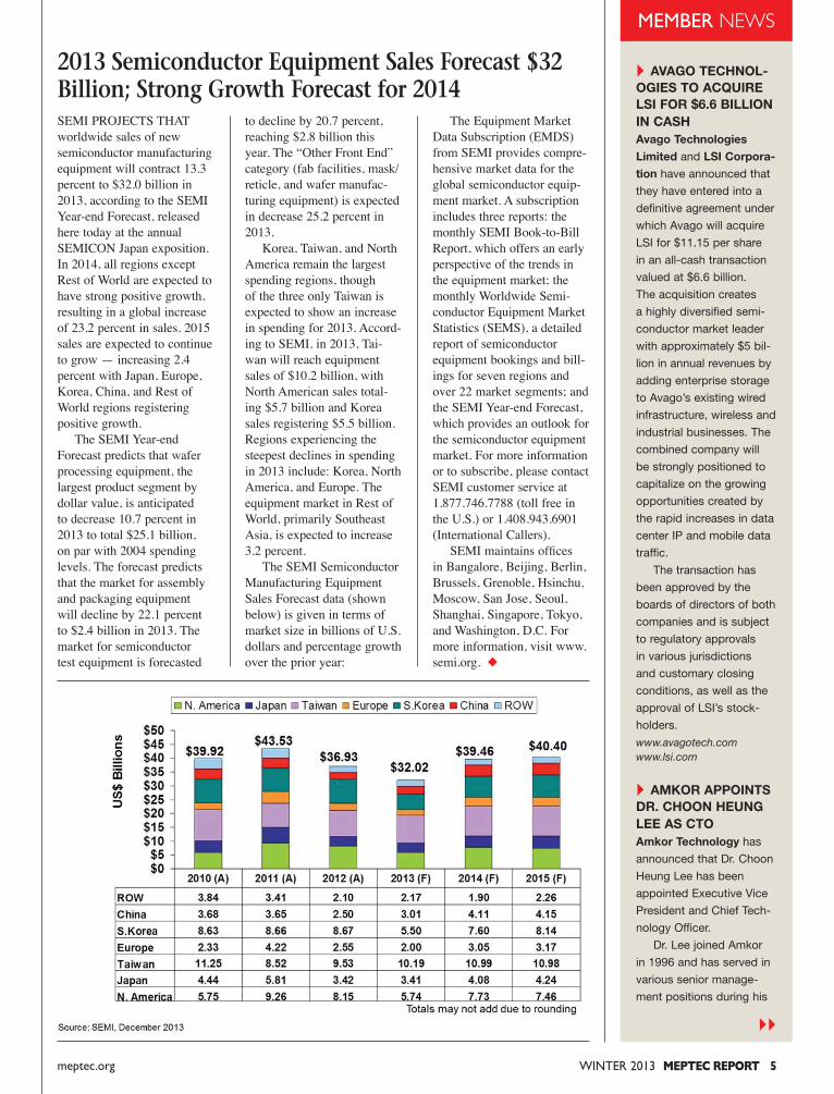
SEMI PROJECTS THAT worldwide sales of new semiconductor manufacturing equipment will contract 13.3 percent to $32.0 billion in 2013, according to the SEMI Year-end Forecast, released here today at the annual SEMICON Japan exposition. In 2014, all regions except Rest of World are expected to have strong positive growth, resulting in a global increase of 23.2 percent in sales. 2015 sales are expected to continue to grow — increasing 2.4 percent with Japan, Europe, Korea, China, and Rest of World regions registering positive growth. The SEMI Year-end Forecast predicts that wafer processing equipment, the largest product segment by dollar value, is anticipated to decrease 10.7 percent in 2013 to total $25.1 billion, on par with 2004 spending levels. The forecast predicts that the market for assembly and packaging equipment will decline by 22.1 percent to $2.4 billion in 2013. The market for semiconductor test equipment is forecasted
WINTER 2013 MEPTEC REPORT 5meptec.org
2013 Semiconductor Equipment Sales Forecast $32 Billion; Strong Growth Forecast for 2014
to decline by 20.7 percent, reaching $2.8 billion this year. The “Other Front End” category (fab facilities, mask/reticle, and wafer manufac-turing equipment) is expected in decrease 25.2 percent in 2013. Korea, Taiwan, and North America remain the largest spending regions, though of the three only Taiwan is expected to show an increase in spending for 2013. Accord-ing to SEMI, in 2013, Tai-wan will reach equipment sales of $10.2 billion, with North American sales total-ing $5.7 billion and Korea sales registering $5.5 billion. Regions experiencing the steepest declines in spending in 2013 include: Korea, North America, and Europe. The equipment market in Rest of World, primarily Southeast Asia, is expected to increase 3.2 percent. The SEMI Semiconductor Manufacturing Equipment Sales Forecast data (shown below) is given in terms of market size in billions of U.S. dollars and percentage growth over the prior year:
The Equipment Market Data Subscription (EMDS) from SEMI provides compre-hensive market data for the global semiconductor equip-ment market. A subscription includes three reports: the monthly SEMI Book-to-Bill Report, which offers an early perspective of the trends in the equipment market; the monthly Worldwide Semi-conductor Equipment Market Statistics (SEMS), a detailed report of semiconductor equipment bookings and bill-ings for seven regions and over 22 market segments; and the SEMI Year-end Forecast, which provides an outlook for the semiconductor equipment market. For more information or to subscribe, please contact SEMI customer service at 1.877.746.7788 (toll free in the U.S.) or 1.408.943.6901 (International Callers). SEMI maintains offices in Bangalore, Beijing, Berlin, Brussels, Grenoble, Hsinchu, Moscow, San Jose, Seoul, Shanghai, Singapore, Tokyo, and Washington, D.C. For more information, visit www.semi.org. ◆
MEMBER NEWS
AVAGO TECHNOL-OGIES TO ACQUIRE LSI FOR $6.6 BILLION IN CASHAvago Technologies Limited and LSI Corpora-tion have announced that
they have entered into a
definitive agreement under
which Avago will acquire
LSI for $11.15 per share
in an all-cash transaction
valued at $6.6 billion.
The acquisition creates
a highly diversified semi-
conductor market leader
with approximately $5 bil-
lion in annual revenues by
adding enterprise storage
to Avago’s existing wired
infrastructure, wireless and
industrial businesses. The
combined company will
be strongly positioned to
capitalize on the growing
opportunities created by
the rapid increases in data
center IP and mobile data
traffic.
The transaction has
been approved by the
boards of directors of both
companies and is subject
to regulatory approvals
in various jurisdictions
and customary closing
conditions, as well as the
approval of LSI’s stock-
holders.
www.avagotech.comwww.lsi.com
AMKOR APPOINTS DR. CHOON HEUNG LEE AS CTOAmkor Technology has
announced that Dr. Choon
Heung Lee has been
appointed Executive Vice
President and Chief Tech-
nology Officer.
Dr. Lee joined Amkor
in 1996 and has served in
various senior manage-
ment positions during his
6 MEPTEC REPORT WINTER 2013 meptec.org
HONEYWELL ELECTRONIC Materials has announced that its PTM series of thermal interface materials (TIM) has been selected as the thermal management solution for a leading gaming platform. The material is being used to manage the tremen-dous heat generated by the semiconductor in the gaming console, helping ensure per-formance and reliability. The latest advanced capabilities of the newest gaming platforms result in elevated chip tem-peratures which can degrade the user experience by slow-ing processor performance, trigger system shutdowns, and in severe conditions, cause permanent hardware damage and data loss. “Both hardcore and casual game players expect reliable performance from their advanced consoles in order to have a satisfying and entertaining experience,” said David Diggs, vice president and general manager for Honeywell Electronic Materi-als. “Because of this, reliable thermal management is essen-tial to ensure that the system functions at its peak level and performs consistently year-in and year-out.” New gaming devices use an Accelerated Processing Unit (APU), a sophisticated system-on-chip that integrates the latest multi-core proces-sors with extremely fast graphic accelerators and dedi-cated memory modules. How-ever, this design produces heat which must be managed to sustain optimal perfor-mance through the service life of the gaming console. Honeywell is a recognized leader in developing thermal management solutions that transfer and dissipate heat from advanced semiconductor devices. Honeywell’s proven PTM series of thermal man-
An Enterprise Software Solution for Managing The Cold Chain
NOLIMITS
Any location.Any time.Any users.
M A R A T H O N P R O D U C T S
800-858-6872 www.marathon products.comDon’t ship without us®
Temperature Data LoggersOperating ranges: -80°C to 72°C. Our devices are programmed in English, Japanese, French, German, Spanish, Mandarin, and Portuguese to support globalization. Make c\temp your last Q.C. gate of product validation prior to accept- ance of critically- sensitive materials for manufacturing.
Marathon Products, Inc. headquartered in San Leandro, CA is a global supplier of investigative temperature recording devices used to validate shipments of epoxies, laminates and other critical materials used in the manufacture of integrated circuits.
An Enterprise Software Solution for Managing The Cold Chain
Honeywell Electronic Materials Selected for Thermal Management of New Gaming Platform
agement materials enables high processing performance under demanding conditions. It is based on a sophisticated phase-change chemistry that was developed specifically for high-performing semicon-ductor devices. Honeywell’s industry-leading TIM technol-ogy transfers thermal energy from the APU to the heat sink and fan module. This critical bridge keeps the APU cool, while allowing the heat sink module to perform optimally. Honeywell’s unique and proprietary formulation provides long lasting chemi-cal and mechanical stability through accelerated aging tests like extended baking at 150°C, thermal cycling from -55°C to +125°C, and the “Highly Accelerated Stress Test” (or “HAST”). This stability enables consistently high thermal performance
long after alternate thermal interface materials break down or dry out. Honeywell Electronic Materials, part of Honeywell Performance Materials & Technologies, supplies micro-electronic polymers, elec-tronic chemicals, and other advanced materials along with an extensive set of product offerings under its metals business segment, including physical vapor deposition (PVD) targets and coil sets, precious metal thermocouples, and low alpha emissivity plat-ing anodes and advanced heat spreader materials used during back-end packaging processes for thermal management and electrical interconnect. For more information, or to contact a Honeywell representative, visit www.honeywell-pmt.com. ◆
MEMBER NEWS
time with the company,
including most recently as
Corporate Vice President,
Business and Technol-
ogy Management. Dr.
Lee also has written 23
research papers on vari-
ous packaging technology
related subjects and has
been granted 26 patents
in Korea and 11 in the
US. He holds a degree
in physics and a Masters
degree in statistical phys-
ics from Korea University,
and a Masters degree
and Ph.D. in physics from
Case Western Reserve
University.
www.amkor.com
TESSERA TECH-NOLOGIES APPOINTS ROBERT ANDERSEN EXECUTIVE VP AND CFOTessera Technologies Inc. has announced the
appointment of Robert J.
Andersen as the Compa-
ny’s executive vice presi-
dent and chief financial
officer (CFO) effective as
of Jan. 2, 2014. Andersen
will report to CEO Thomas
Lacey and be responsible
for the Company’s finance,
accounting, strategic plan-
ning, investor relations and
IT. John Allen, who had
served as the Company’s
acting CFO since June
2013, returned to his prior
position as the Company’s
senior vice president and
corporate controller.
Andersen holds a B.A.
in Economics from the
University of California,
Davis, and an M.B.A. from
the Anderson School of
Management at the Uni-
versity of California, Los
Angeles.
www.tessera.com
WINTER 2013 MEPTEC REPORT 7meptec.org
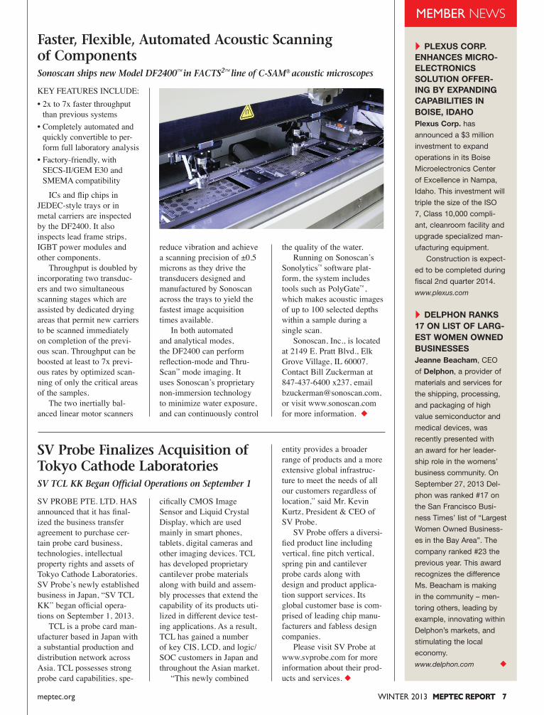
KEY FEATURES INCLUDE:• 2x to 7x faster throughput • than previous systems• Completely automated and • quickly convertible to per- • form full laboratory analysis• Factory-friendly, with • SECS-II/GEM E30 and • SMEMA compatibility
ICs and flip chips in JEDEC-style trays or in metal carriers are inspected by the DF2400. It also inspects lead frame strips, IGBT power modules and other components. Throughput is doubled by incorporating two transduc-ers and two simultaneous scanning stages which are assisted by dedicated drying areas that permit new carriers to be scanned immediately on completion of the previ-ous scan. Throughput can be boosted at least to 7x previ-ous rates by optimized scan-ning of only the critical areas of the samples. The two inertially bal-anced linear motor scanners
reduce vibration and achieve a scanning precision of ±0.5 microns as they drive the transducers designed and manufactured by Sonoscan across the trays to yield the fastest image acquisition times available. In both automated and analytical modes, the DF2400 can perform reflection-mode and Thru-Scan™ mode imaging. It uses Sonoscan’s proprietary non-immersion technology to minimize water exposure, and can continuously control
the quality of the water. Running on Sonoscan’s Sonolytics™ software plat-form, the system includes tools such as PolyGate™, which makes acoustic images of up to 100 selected depths within a sample during a single scan. Sonoscan, Inc., is located at 2149 E. Pratt Blvd., Elk Grove Village, IL 60007. Contact Bill Zuckerman at 847-437-6400 x237, email [email protected], or visit www.sonoscan.com for more information. ◆
SV PROBE PTE. LTD. HAS announced that it has final-ized the business transfer agreement to purchase cer-tain probe card business, technologies, intellectual property rights and assets of Tokyo Cathode Laboratories. SV Probe’s newly established business in Japan, “SV TCL KK” began official opera-tions on September 1, 2013. TCL is a probe card man-ufacturer based in Japan with a substantial production and distribution network across Asia. TCL possesses strong probe card capabilities, spe-
SV Probe Finalizes Acquisition of Tokyo Cathode LaboratoriesSV TCL KK Began Official Operations on September 1
cifically CMOS ImageSensor and Liquid Crystal Display, which are used mainly in smart phones, tablets, digital cameras and other imaging devices. TCL has developed proprietary cantilever probe materials along with build and assem-bly processes that extend the capability of its products uti-lized in different device test-ing applications. As a result, TCL has gained a number of key CIS, LCD, and logic/SOC customers in Japan and throughout the Asian market. “This newly combined
entity provides a broader range of products and a more extensive global infrastruc-ture to meet the needs of all our customers regardless of location,” said Mr. Kevin Kurtz, President & CEO of SV Probe. SV Probe offers a diversi-fied product line including vertical, fine pitch vertical, spring pin and cantilever probe cards along with design and product applica-tion support services. Its global customer base is com-prised of leading chip manu-facturers and fabless design companies. Please visit SV Probe at www.svprobe.com for more information about their prod-ucts and services. ◆
Faster, Flexible, Automated Acoustic Scanning of ComponentsSonoscan ships new Model DF2400™ in FACTS2™ line of C-SAM® acoustic microscopes
MEMBER NEWS
PLEXUS CORP. ENHANCES MICRO-ELECTRONICS SOLUTION OFFER-ING BY EXPANDING CAPABILITIES IN BOISE, IDAHO Plexus Corp. has
announced a $3 million
investment to expand
operations in its Boise
Microelectronics Center
of Excellence in Nampa,
Idaho. This investment will
triple the size of the ISO
7, Class 10,000 compli-
ant, cleanroom facility and
upgrade specialized man-
ufacturing equipment.
Construction is expect-
ed to be completed during
fiscal 2nd quarter 2014.
www.plexus.com
DELPHON RANKS 17 ON LIST OF LARG-EST WOMEN OWNED BUSINESSESJeanne Beacham, CEO
of Delphon, a provider of
materials and services for
the shipping, processing,
and packaging of high
value semiconductor and
medical devices, was
recently presented with
an award for her leader-
ship role in the womens’
business community. On
September 27, 2013 Del-
phon was ranked #17 on
the San Francisco Busi-
ness Times’ list of “Largest
Women Owned Business-
es in the Bay Area”. The
company ranked #23 the
previous year. This award
recognizes the difference
Ms. Beacham is making
in the community – men-
toring others, leading by
example, innovating within
Delphon’s markets, and
stimulating the local
economy.
www.delphon.com ◆
8 MEPTEC REPORT WINTER 2013 meptec.org
Act of 2010. The bill required that U.S. public companies provide a report if any of their products contain conflict miner-als that were sourced in the DRC or adjoining countries. It also stated that the company had responsibilities to deter-mine the source and chain of custody of those minerals and that there must be an independent private sector audit of the report. It was determined that this require-ment would be administered by the U.S. Securities and Exchange Commission (SEC). The SEC developed policies and procedures to administer Section 1502. There were hearings and modifications and the Final Ruling was passed by the SEC on August 22, 2012 and issued as a 356 page document.
Filing Requirements The first filing year is 2013, begin-ning on January 1, 2013 and ending on December 31, 2013. The first filing is due on or before May 31, 2014. If a public company produces products that include Ta, Sn, W or Au, a determination must be made as to whether any of these minerals were sourced from the Conflict Countries (the DRC plus the 9 adjoining states). This process is referred to as a Reasonable Country of Origin Inquiry (RCOI) and must be performed in accor-dance with an internationally recognized framework, such as the OECD Guide-lines for Multinational Enterprises. If there is reasonable doubt as to the source of the conflict minerals, a more detailed due diligence effort must be undertaken to determine the source with as much specificity as possible. A public company does NOT have to become conflict free, but they must fol-low the procedures outlined in the SEC Final Rule. Though the RCOI and due diligence work is very much supply chain oriented, the actual SEC filing is by product or product group. This requirement adds significantly to the complexity of the compliance effort.
Public vs. Private On the surface, it would appear that private companies in the semiconductor supply chain do not get involved, but this is far from the truth. Because public companies, semiconductor or otherwise, must trace their supply chain down to the Smelter or Refiner (SoR) level, they must “pass through” private companies in the chain. While there is no legal
COLUMN
PROFITS FROM CONFLICT minerals found in the Democratic Repub-lic of the Congo (DRC) have supported conflict, human rights violations and labor and environmental abuses in the region for years. Though the recent sur-render of the Congolese Revolutionary Army provides some hope for the future, the group was only recently formed and it is widely recognized that it did not create the conflict minerals problem. Fifty armed groups remain, ranging in size from thousands of members to dozens that are involved in one way or another with conflict minerals. Compa-nies that use these minerals in the design and manufacture of their products and components are concerned about these abuses, and are taking action to avoid contributing to conflict in any way. The U.S. Government is helping through leg-islation and regulations. Conflict minerals include cassiterite, columbite, tantalite, wolframite and their derivative elements tin (Sn), tantalum (Ta) and tungsten (W) as well as gold (Au), regardless of their source in the world. Collectively these minerals and elements are referred to by the acronym 3TG. The DRC is the size of Texas and Alaska combined with a population of 75 million who are among the poorest peo-ple in the world. The DRC has mineral reserves of $24 trillion, the richest of any country in the world. The country has been in a civil war for 15 years and mil-lions of people have been killed during that time. The death rate remains very high due to violence and the sickness and starvation exacerbated by it.
Legislation A rider (Title XV, Section 1502) was attached to the U.S. Dodd-Frank Wall Street Reform and Consumer Protection
Conflict Minerals in the Semiconductor Industry
INDUSTRYINSIGHTSBy Ron Jones
requirement to participate, there is pres-sure from upstream customers to support the conflict minerals compliance effort. Private companies need to do the RCOI and due diligence work in order to pro-vide information to their customers. The difference is that they do not need to file with the SEC.
Conflict Minerals in the Semiconductor Industry For an integrated circuit (IC) to be conflict free, both the die and the pack-age must be conflict free. If the die is conflict free and the package is not, the IC is not conflict free. A simple IC die with but a few levels may not contain any conflict minerals. As the chip gets more complex with more levels, the probability goes up that tungsten, gold or tantalum may be included. Package assembly has a generally higher prob-ability of containing conflict minerals due to materials such as gold bond wire, tin content in lead finish or solders balls for package to board connections. It is highly unlikely that an IC of any signifi-cant complexity will be free of all con-flict minerals.
Semiconductor Supply Chain Structure First, we have a semi-fixed set of resources that produce die and a semi-fixed set of resources that do packaging. A few fabs (captive or foundry) are built and shut down each year, but there is stability and their identity is known on a worldwide basis. The same is true for assembly operations (captive or OSAT). This means that virtually all IC’s are manufactured by a known set of facto-ries. This is far different than products, like computers or airplanes, that have many levels in their bill of material and whose supply chain includes myriad manufacturers or fabricators around the world. Fabless companies have about 75 foundry and 75 OSAT companies from which to choose. This means that the potential exists for information col-lected about Foundry X or OSAT Y to be shared by many fabless companies. Second, the direct materials used in semiconductor manufacturing are typical-ly very high purity. In fab, WF6 process gas or TiW sputtering targets are used and are highly controlled for content and purity. In assembly, gold bond wires have tightly controlled composition. Even Tin, used in lead finish or package connec-tion, is controlled for contamination and consistency. The use of high purity direct
WINTER 2013 MEPTEC REPORT 9meptec.org
Ron Jones is CEO of N-Able Group International; a semiconductor focused consulting and recruiting company. N-Able Group utilizes deep semi supply chain knowledge and a powerful cloud based software application to provide Conflict Min-eral Compliance support services to companies throughout the semicon-ductor supply chain including fabless, foundry, OSAT and materials suppli-ers. Visit www.n-ablegroup.com or email [email protected] for more information.
materials puts the industry in close prox-imity to the smelters and refiners that must be tracked.
What Needs to be Done? Many companies believe that conflict minerals compliance consists of noth-ing more than gathering EICC-GeSI forms from first tier suppliers. This is merely the tip of the iceberg, however. The RCOI in the SEC Rule requires that companies track the conflict minerals to the smelter or refiner. Depending on the RCOI outcome, a much more in-depth due diligence analysis may be required. The outcome of these processes will determine whether a third party audit is required. Public companies must file these documents with the SEC. Private or public companies need to provide this information to their customers who must include it in their filing.
Alternate Approach Conflict minerals reporting is an ongoing requirement that will likely grow in scope over time. It is not a core competency and does not provide a value add to semiconductor companies at any
Underfi ll for Your Current and Future Requirements
NAMICS is a leading source for high technology underfi lls, encapsulants, coatings and specialty adhesives used by producers of semiconductor devic-es. Headquartered in Niigata, Japan with subsidiaries in the USA, Europe, Singapore and China, NAMICS serves its worldwide customers with enabling products for leading edge applica-tions.
For more information visit our website or call 408-516-4611
www.namics.co.jp
SMT, COB, COF, IC ASSEMBLYSAME DAY, 1 - 5 DAYS TURN
— SMT ASSEMBLY, Lead-Free, 0201, uBGA, CSP— COB, COF, IC ASSEMBLY, Cleanroom ISO 7 (Class 10,000), Aluminum and Gold wire— NPI - PROTOTYPE, 8, 24 to 72 hours turn— Low to Medium Volume PRODUCTION, MRP, IPC-A-610 Class 2 and 3, MIL-STD-883
Your NPI Manufacturing Solution!
Phone (408) 227-8885Email: [email protected]
AmTECH is a leadingSilicon Valley providerfor SMT, COB, COF andIC Assembly.
Gold ball, aluminumand gold wedge wirebonding, AutomatedOptical Inspection(AOI) and XRAY.
www.amtechmicro.com
(866) 404-8800
www.MirrorSemi.com
Open CavityQFN
YourDie
Here
Fabless • MEMS • RF • Sensors
“Time Critical” Organic Substrates
BGA, CSP, Flip Chip, High Frequency, High Speed, Rigid, Cavity and
Flex Packages- 15µm Lines and Spaces -
ACL is the onlyNorth American company
focusing exclusively on the fabrication of
High Density Interconnects.ITAR Registered
Phone: 408.327.0200 Email: [email protected]
www.aclusa.com
AdvancedComponentLabs, Inc.
level. The work may be performed by each individual company with great duplication of effort, or performed by specialists to reduce redundancy. The unique nature of the IC supply chain and bill-of-materials structure enables the semiconductor industry to be leaders in the efficiency of conflict minerals compliance if they will work together. This is good not only for our industry, but for the greater electronics supply chain. ◆
10 MEPTEC REPORT WINTER 2013 meptec.orgmeptec.org
COLUMN
Electronic coupling is the transfer of ener-gy from one circuit or medium to another. Sometimes it is intentional and sometimes not (crosstalk). I hope that this column, by mixing technology and general observa-tions, is thought provoking and “couples” with your thinking. Most of the time I will stick to technology but occasional cross-talk diversions like this one may deliver a message closer to home.
WHATEVER YOU DESIRE “THERE’S an app for that!” Dream big or small, it is very likely a software program is already available. But what if you dream in hardware? Hewlett-Packard is build-ing applications with one MILLION sen-sors. Robert Bosch is dreaming of 1,000 sensors per person, i.e. seven TRILLION. Janusz Bryzek is aiming for one TRIL-LION per year. Standardized smartphone hardware platforms and application “stores” have significantly lowered the cost and time to develop and sell applications. One might argue the barrier to entry is too low - some applications are developed in a weekend for pennies and it shows… What works well for software, where larger investments can be delayed until market interest is confirmed, is simply not practical for most hardware appli-cations. Hardware has high development costs especially if they are micro-elec-tromechanical systems (MEMS) based products. MEMS devices on average cost as much as $30-45 M and can take 25-30 years for full commercialization. For hardware applications it is essential to understand the product and market requirements (including likely customer demand) beforehand. The inaugural TSensors Summit recently held at Stanford University was focused on how to identify the markets and requirements for high-volumes of sensor based hardware. Most, if not all, of these hardware sensor solutions would be MEMS based to provide high func-tionality at low costs in extremely high volumes. The organizing committee, on
which I serve, has the goal to build a pro-cess to generate an industry roadmap to achieve a trillion (“T”) sensors. As the driving force behind TSensors, Janusz Bryzek (Vice President Development, MEMS and Sensor Solutions of Fairchild Semiconductor and Chairman of the event) wants to achieve large volumes not for their own sake but for “abundance”. In Abundance; The Future Is Better Than You Think (2012), Peter Diamandis and Steve Kotler describe solving global problems using technology to achieve balance between supply and demand. This abundance – providing “a world of nine billion people with clean water, nutritious food, affordable housing, personalized education, top-tier medical care, and non-polluting, ubiquitous energy” – is what Bryzek wants to achieve. And Diamandis and Kotler know they need high technol-ogy including sensors, possibly needing as many as forty-five trillion sensors in the next twenty years. (Well in excess of 1 T per year at the high end of the estimate…) The end markets are clear: medicine, food production, energy, and water. Therefore, what is needed is to define the specific applications in order to focus companies on building the necessary software and hardware. Yes, there will be software only solutions that will make a difference but the biggest impact will come from hardware-centric or hard-ware-enabled (combined with software) systems. The challenge is how to develop this hardware as quickly as possible and build at scale while providing the proper return on investment. The race is on to have these solutions before the world adds another billion or two people… Clearly the current MEMS devel-opment paradigm is too long at 25-30 years and too expensive at $25-30M per MEMS device and even more for the entire application system. Therefore, the industry needs to accelerate this work through “coopetition” (cooperation with competition) including the generation of roadmaps. Roadmaps help an entire industry identify needs and timing to ensure a healthy ecosystem of suppliers and customers. As an example, the semi-conductor industry has flourished through the annual publication of International Technology Roadmap for Semiconductors (ITRS) since 1998 identifying the needs and challenges of the next fifteen years. The goal of the TSensors community is to build a similar roadmap for sensors. A comprehensive roadmap would identify the technology required for the desired
A Trillion Sensors?
COUPLING & CROSSTALKBy Ira Feldman
functionality and timing. This would enable suppliers and customers to align their schedules and expectations so nei-ther would get too far ahead of the other. A mismatch is not good – having a tech-nology that no one is ready to buy and not having the technology available when customers need it are equally problematic. Over three days, the TSensors Summit had forty-six excellent presentations from leading visionaries of the sensor world covering a very wide array of markets and applications. Challenges discussed includ-ed everything from basic technology to business issues to customer education to regulatory approval. What quickly became apparent is the need to converge solutions by creating general-purpose sensor platforms. Steve Nasiri (Founder of InvenSense, now running Nasiri Ventures) described how InvenSense disrupted the market by shifting from a single-axis inertial mea-surement device (gyroscope or acceler-ometer) to a motion-sensing platform. Previously to build a product solution required multiple single-axis devices (one for each direction) that had to be properly mounted and calibrated into the end product (video game system, smart-phone, etc.). The end product developer also needed to write the software to read the raw data from each sensor and inter-pret the results. InvenSense moved from single-axis MEMS sensors to providing 6-axis (and greater) MEMS devices along with the software required to provide meaningful motion data. This greatly reduced the development efforts and manufacturing costs while increasing the functionality and value of the InvenSense solution. The shift to supplying plat-forms that are general purpose moved InvenSense from being a component sup-plier to a solution provider. The need for sensor platforms can also be clearly illustrated by examin-ing the area of chemical sensing. If we presume there are two hundred different chemical sensing applications in the next ten years all with the potential for high volume, which scenario is easier: design-ing and building two hundred different sensor technologies or building a generic integrated sensor platform that can handle many or all of them? There are several companies, including Hewlett-Packard, currently working on MEMS based Raman spectrometers to cost effectively identify a large number of chemicals. The ultimate goal is to make these MEMS sensors inexpensive enough that they
WINTER 2013 MEPTEC REPORT 11meptec.org
Silicon Valley’sPackaging Foundry
www.promex-ind.com+1.408.496.0222
IC Assembly & PackagingQFN’s • Over Molded • Open Cavity
Advanced PackagingDevelopment • NPI • Production
ISO 13485:2003 Medical Class 100 Clean Room ITAR Registered IPC-A-610 Class 3 Assembly
IRA FELDMAN ([email protected]) is the Principal Consultant of Feldman Engineering Corp. which guides high technol-ogy products and services from concept to commercialization. He follows many “small technologies” from semiconductors to MEMS to nanotechnology engaging on a wide range of projects including product generation, marketing, and business development.
become disposable. Volunteers are working to identify the number of distinct platforms (and require-ments) to service all the different sensing needs discussed at TSensors and those already known to them. For each type of platform identified a working group will be formed. The working groups will identify the technology requirements along with the development work and ecosystem support required to rapidly commercialize the platform. Estimation of the current progress towards commer-cialization and gaps will be made for each platform type. It is true that some platforms may initially be more expensive as “general purpose” versus application specific. However, it is hoped that platforms shorten the time to market for a wider array of products with significantly lower development cost across all applications. The platforms should also have lower overall costs due to economies of scale and competition between different sup-pliers building platforms for the same markets. And as platforms provide higher value solutions versus simply supplying components they should also speed devel-opment while lowering product costs. Now is a great time to get involved in this roadmap effort from providing input, writing requirements, or determin-ing your company’s market strategy! We welcome participation at one of the six or so events in 2014 including additional Summits in Japan, China, and Germany. And we look forward to adding work-ing group members to drive the platform definitions. Our goal is to complete a first revision of the roadmap before the next United States TSensors Summit in October 2014. Please see http://www.tsen-sorssummit.org/ to engage in the process and for additional details. As always I encourage your questions and comments on my blog http://high-techbizdev.com. ◆
High-mix, high-precision, low to medium volume production of CNC machined components. We’ve got you covered.
• Robotic Cell Machining• Horizontal / Vertical Milling• CNC Turning
• Prototyping
• Kitting
• Real-Time SPC Quality Control
(503) 625.2821 | Treske.com
AS9100C | ITAR Registered | ISO9001:2008
redefiningamerican machining
www.masterbond.com
154 Hobart Street, Hackensack, NJ 07601 USA+1.201.343.8983 • [email protected]
• Electrically insulative• Cures at room temperature• NASA low outgassing approved• Halogen free• High/low temperature resistant
Two Component EP21TCHT-1
Thermally ConductiveEpoxy Adhesive
12 MEPTEC REPORT WINTER 2013 meptec.org
FOLLOW-UP
EST, EDPS, GSA, IPC and SEMI) intro-duced their teams’ missions and outlined how they work with industry experts from member companies to prioritize the organizations’ efforts and steer them towards common goals, like important recommendations, best practices and even industry standards. In summary: The new format – four panel sessions – invited much more inter-action between presenters and audience compared to previous events. It prompted many more questions, triggered more ideas and yielded thoughtful comments from both panelists and audience mem-bers. Most importantly, this Roadmaps Symposium not only encouraged a more constructive dialog between companies, but also gave a great example for the value of joint problem solving. The following sections of this article give more details about the four panels and the keynote.
Panel 1: Product Drivers The Panel 1 experts were led by Joel Camarda, Amonix, as moderator, with panelists Mudasir Ahmad, Cisco; Far-shad Ghahghahi, LSI; Larry Kinsmen, Aptina; Tom Strothmann, STATSChip-PAC; and Suresh Upadhyayula, Sandisk, providing their learned perspectives and observations. Ahmad said Cisco is looking at dis-ruptions in the network space as the likely source for new business opportuni-ties, particularly in video; Cisco projects that 91% of future internet traffic will be video. Cisco’s broad targets are to make products with 10X better performance @ ½ the cost @ 5 times the reliability as products today. On the reliability side, Ahmad observed that reliability is becoming segmented, and that custom-ers may want to choose a certain level of reliability just as they now choose levels of equipment performance.
com, Cisco, Microsoft, Nvidia, SanDisk, Xilinx) gave broad pictures of their mar-kets’ requirements, while the medium and smaller companies focused on their market segments and core competencies. Packaging and Test experts from Amkor and STATSChipPAC showed how broad
their portfolios are and how surface-mount technology, wafer-level packag-ing, interposers and vertical die stacking pave the road to more functionality in smaller spaces. Were there any common threads in these presentations? Yes, as mentioned above, the call for closer cooperation up and down the supply chain was the most common topic during the day. The eSilicon representative even mentioned that addressing supply chain challenges is their major role and business focus, and has been for years already. He also explained why this difficult role has been needed in the past and how it will become more important and more chal-lenging in future. Industry collaboration was the focus of the fourth and final panel session. Speakers from five organizations (CAM-
2013 MEPTEC Semiconductor Roadmaps Symposium
MEPTEC HELD THIS YEAR’S Roadmaps Symposium on September 24 at the Biltmore Hotel in San Jose. As usual it was very well attended; about 150 industry experts dedicated an entire day to outlining their views and require-ments for validation and insight into technology and business directions for their companies as well as to discuss ideas for possible solutions. Networking between attendees, and with exhibitors, filled the breaks. The new symposium format this year - four panel sessions which included brief presentations and plenty of time for Q & A - really engaged the panelists and the audience in lively discussions about industry trends, market needs, ongoing developments, and new products, as well as why and where more joint efforts between companies are needed. In particular, the keynote speaker, Karen Savala, President of SEMI Ameri-cas, emphasized why our industry needs more cooperation and coordination. She described, using many examples, how SEMI is contributing worldwide to mak-ing our ecosystem stronger and more profitable. In response to the rapid progress in silicon technologies – towards smaller feature sizes and larger die – the sympo-sium showed that the packaging and test industry is not only keeping pace with these challenges, but also has developed and is offering a wide range of new solu-tions to integrate more functionality into smaller spaces, enabling higher perfor-mance at lower power and less cost. The four panel sessions, Product Drivers, Manufacturing Drivers, Electri-cal Performance Requirements, and Importance of Industry Collaboration were structured to mix presentations and discussions of our industry’s challenges and opportunities from very different perspectives. The panelist from large IC vendors and system houses (Broad-
Herb Reiter, eda 2 asic ConsultingPaul Werbaneth, 3D InCites
Output (2) at 300% of File Size. Final Trimmed Size 25.5” x 33”. Mount on 3/16” White Foam Board. No Lamination.
2013 MEPTEC SEMICONDUCTOR ROADMAPS
SYMPOSIUMA Collaborative Update from Standards Bodies,
Industry Groups, and the Entire Supply Chain
Media Sponsors
S E P T E M B E R 2 4 , 2 0 1 3 • S A N T A C L A R A , C A L I F O R N I A
Participating Companies:
n Altera Corporation
n Amkor Technology, Inc.
n Amonix Inc.
n Aptina Imaging Corporation
n Broadcom Corporation
n Cadence Design Systems
n Cisco Systems Inc.
n eda2asic Consulting, Inc.
n eSilicon Corporation
n Invensas Corporation
n IPC
n LSI Corporation
n Microsoft Corporation
n NVIDIA Corporation
n PPM Associates
n SanDisk Corporation
n SEMI
n STATSChipPAC, Inc.
n SVXR
n TechSearch International, Inc.
n Xilinx Inc.
Gold Sponsor
Association Sponsors

WINTER 2013 MEPTEC REPORT 13meptec.org
Keynote: Karen Savala, SEMI, on The Collaboration Engine: Enabling Innovation in Microelectronics As keynote speaker, Savala’s message was “The history of semiconductors has been a history of collaboration.” SEMI realized that an industry-wide collaborative approach to 3D stacked ICs was needed to reach widespread 3D-IC adoption, recognizing that “The industry has been excited about More-Than-Moore applications, especially 3D stacked ICs that promise to improve bandwidth, reduce footprint, decrease power consumption, and lower cost.” To that end, SEMI established stan-dards task forces for thin wafer handling, and for inspection and metrology, with the participation of task force members from Qualcomm, Applied Materials, Semilab, NIST, ASE, Xilinx, and others. According to Savala: “For 3D-IC to be widely adopted, meaningful collabo-ration throughout the value chain still needs to occur.” “Without the emergence of a new, robust collaboration model that can deliver meaningful agreements between key constituencies, the promise of 3D innovation will remain distant and illu-sive.” “Standards work helps, but a new model is needed to make 3D IC afford-able.”
Panel 3: Electrical Performance Requirements Ivor Barber from Xilinx and John Xie from Altera co-moderated this panel and showed how line rate and bandwidth have to increase, to keep pace with mar-ket demand. They also showed that all these advancements have to be achieved while reducing power and cost. (Special thanks to Scott Jewler from SVXC for professionally summarizing the panel at the end of the day.) Broadcom’s Tom Gregorich was first to present. After giving a few examples of impressive system advancements, he reminded us that Moore’s Law needs to be complemented and/or replaced with other innovations to sustain the high growth rate of our industry. Knowing that this will be a big challenge, he closed with telling us Jonah’s Law: “Swim fast, eat everything around you or be eaten!” Brad Griffin from Cadence presented next. He eased our minds by mentioned several features and benefits Cadence’
ble rather than invest in a new TSV eco-system. On the contrary, said STATSCh-ipPAC, TSV is here now – we have the technological capability, but it’s a matter of getting the cost right.
Panel 2: Manufacturing Drivers in Semiconductor Roadmaps Jeff Demmin, STATSChipPAC, started Panel 2 with a show-and-tell collection of cast-aside devices from his personal electronics museum. Responding to Jeff’s leads were panelists Richard Crisp, Invensas; Javier DeLaCruz, eSilicon; Ron Huemoller, Amkor; Raj Master, Microsoft; and Dongkai Shangguan, NCAP China. (Linda Matthew, TechSearch Inter-national, summarized Panel 2 and pre-sented those results at the end of the day; thank you Linda for your very helpful notes.) Three topics of interest during the Panel 2 discussion, from a high level, were TSV and multi-die packaging and form factors; photonics (it’s coming, or it’s already here); and reliability. Many of the TSV commercialization challenges were said to be supply chain and business model challenges; funda-mentally “who is going to be the integra-tor?” Yield management with multi-die TSV packaging may be a bigger issue than is the technology of how to actually build TSVs. DeLaCruz said achieving 100% yield is not a reasonable target on large 2.5D or 3D packages. What’s critical is having well-understood yields, even if those yields are something like 60%. So, whither TSV? Huemoller said memory won’t be the big play for early implementation of TSV; rather, it will be the de-partitioning of logic at the 14 and 16nm nodes that will be the primary driver for TSV implementation in value markets, with true 3D packages featur-ing stacked memory with TSVs hitting the market in the 2016/17 timeframe, delayed by cost. On cost, Shangguan spoke of the work NCAP is doing in developing wafer fab equipment optimized for packaging as a way to come up with lower cost alternatives to 2.5D solutions. Shang-guan’s perspective is that the supply chain for interposers will evolve and mature, just as the supply chain for organic substrates has done.
Widening operating temperature may be a useful area for development; since it takes as much power to cool electronic products as it does to run them, sustain-ing higher temperatures creates an oppor-tunity to save operating costs. For advanced packaging and intercon-nects, Cisco thinks the end game may not be TSV / 3D IC, but maybe silicon photonics instead, to reduce interconnect delays and power. LSI Corporation focuses on data transfer and storage using ASIC and SoC products. According to Ghahghahi, LSI’s new product driver challenges include form factor reduction, achieving finer BGA pitches, increasing I/O capabilities of their chips, and decreasing package heights to below 1mm. Ghahghahi agreed there is a need for things like new materials, or other ways to accommodate thermal handling in packaged chips, where power on the order of 100W+ needs to be dissipated And LSI too is taking a look at 2.5D and silicon photonics. Aptina is a CMOS imaging company in a chip and algorithms market with expected 17% CAGR. Regarding pack-aging, Kinsmen let us know that wire bonding is still prevalent in the industry, but Aptina introduced TSVs and made a product crossover more than a year ago. The Apple iPhone, for example, has a stacked chip solution where the image sensor is mated to the coprocessor using wafer-to-wafer 3D interconnects. The harsh reality of the imaging business is the constant need to drive performance up, but it can’t cost more, because customers don’t buy parts based on performance alone. “Cost, cost, cost,” is what drives STATSChipPAC. Mobile device markets demand cost reductions above all things, said Strothmann, and no one can develop exotic solutions to wafer fabrication or packaging without considering cost. Reliability for mobile applications has some wiggle room, the expectations for reliability being lower in the mobile market, with low-end suppliers in China producing devices specifically for the China market driving this trend. Per the audience, during Q&A, “The TSV roadmap keeps getting pushed out. Beyond optical sensors and memory what’s next for TSV?” According to Cisco, it’s better to stay with silicon monolithic technology as long as possi-
14 MEPTEC REPORT WINTER 2013 meptec.org
FOLLOW-UP
Ken also presented Cadence’ view of how and when 3D-ICs will evolve to meet our industry’s requirements. Jasbir Bath, principle engineer at IPC, brought us back to hardware. He introduced the 50+ year-old Institute for Printed Circuits (IPC), impressed us with its size (3000+ members) and explained why industry-wide cooperation continues to gain importance. Jasbir also described the ongoing efforts in support of 2.5/3D-IC packaging. Last, but not least, Paul Trio from SEMI briefly summarized what Karen Savala had told us about this large and powerful organization three hours earlier, then outlined SEMI’s focus on manu-facturing challenges and showed a long list of services SEMI offers its 4500+ members. Paul highlighted SEMI’s con-tributions to 450 mm wafers, 3D-ICs and EHS (Environmental Health and Safety) and listed many of SEMI’s achievements. In the Q & A session focusing on industry collaboration the audience agreed that cooperation and jointly-developed standards are important, but their questions demonstrated that – unless encouraged by their management – engineering experts are hesitant to dis-cuss this topic. This very typical reaction from engi-neering experts demonstrated that the value of industry-wide collaboration needs to be first “sold” to a company’s management, approved by them and conveyed to engineering, before their technical experts can be expected to col-laborate. ◆
Proceedings and presentations from the 2013 MEPTEC Semiconductor Road-maps Symposiums are available for pur-chase on the MEPTEC website at www.meptec.org/mepteccdlibrary.html. For more information contact Bette Cooper at [email protected].
teria. It showed that our industry is com-mitted to keeping up the pace of innova-tion.
Panel 4: Importance of Industry Collaboration Phil Marcoux from PPM Associates moderated the last panel. After introduc-ing the panelists, he reminded us that R&D efforts in packaging and test are also becoming more challenging and very costly. Even large companies can no longer afford to finance and execute the required R & D in-house, nor can they exert enough market pull to turn the entire supply chain into a strong and cost-effective enough ecosystem in sup-port of a new technology – e.g. 3D-ICs. (Special thanks to Hongxia Sun and Bernhard Adams from STATSChipPAC for summarizing the panel very thor-oughly at the end of the day.) Dieter Bergman, as IPC ambassa-dor, presented for Dennis Fritz, an IPC committee chairman. Dieter introduced CAMEST, a packaging-focused coalition within IPC, and described their mem-bers’ wide-ranging activities and goals. Herb Reiter from eda 2 asic Consult-ing represented the EDA-focused EDPS organization. He described the IC- and system-design focused topics EDPS addressed in previous years and shared the organizing committee’s objectives for this conference. Herb showed how many major companies typically participate to discuss and agree upon design tools and flow requirements. He encouraged the audience to join the next EDPS con-ference in Monterey, CA, in mid-April 2014. As chair of the GSA’s 3D-IC Working Group, Ken Potts from Cadence out-lined this group’s objectives and the key benefits 3D-ICs offer. He described how Cadence tools contribute to addressing design and manufacturing challenges.
EDA tools offer the stressed IC-, pack-age-, board- and system designers. How-ever, he then made us aware that most companies nowadays require smaller engineering teams to complete larger designs, allowing less development time. When he compared these challenging scenarios with “juggling on a tight rope while riding on a unicycle” all designers in the room nodded in agreement. Anthony Torza from Xilinx quantified most of the challenges previous speak-ers mentioned, with actual data such as: Internet bandwidth needs to double every three years; video occupies the lion share of the internet’s capacity. He listed sev-eral challenges for wireless applications: Higher frequencies, new and faster com-munication standards, and higher levels of integration to achieve smaller and lower cost solutions. Anthony also men-tioned that power dissipation can never be low enough. For managing internet traffic at data centers, Xilinx’ wire-line customers demand more lines with higher speed serial links, at lower power, lower cost and in smaller spaces. Nvidia’s Abe Yee added yet another perspective – Graphics – to our list of demanding applications. For Nvidia’s GPUs, performance needs to double every two years. GDDR5 interfaces won’t be able to keep up with this requirement, 2.5/3D-IC technology and High Bandwidth Memory (HBM) will be needed to continue Nvidia’s pace of inno-vation. Nvidia’s wireless roadmap also shows a clear need for 3D-IC technology (Wide I/O) to offer customers higher resolutions for the increasing screen sizes in mobile devices. Our panelists received many ques-tions about the information they had pre-sented, and every one of them elaborated in greater depth on the topics raised. It was interesting to see that nobody argued about the need for meeting all these cri-
MEPTEC Symposium Proceedings on CD
9.27.11A S U C A M P U S • T E M P E • A R I Z O N A
2011Medical Electronics
Symposium / Day One
Vital Technologies for Health
MEPTEC&SMTAPRESENT
Microelectronics Packaging & Test Engineering Council S
urface Mount Technology Association
In Association With
A S P E C I A L T W O - D A Y T E C H N I C A L S Y M P O S I U M
A S P E C I A L O N E - D A Y T E C H N I C A L S Y M P O S I U M
11.9.11S A N T A C L A R A • C A L I F O R N I A
Presented by
2.5D, 3D and Beyond
Bringing 3D Integration
to the Packaging Mainstream
A S P E C I A L O N E - D A Y T E C H N I C A L S Y M P O S I U M
11.10.11S A N T A C L A R A • C A L I F O R N I APresented by
KGD2011
KNOWN GOOD DIEIn an Era of Multi-Die Packaging and 3D Integration
A S P E C I A L O N E - D A Y T E C H N I C A L S Y M P O S I U M
The Heat Is On
2012 Revolutionary and Evolutionary
Innovations in Thermal Management
3.19.12S A N J O S E • C A L I F O R N I A
Presented by
A S P E C I A L O N E - D A Y T E C H N I C A L S Y M P O S I U M
5.23.12S A N J O S E • C A L I F O R N I A
Presented by
Tenth Annual
MEMS Technology SymposiumSensors: A Foundation for Accelerated MEMS Market Growth to $1 Trillion
9.26.12A S U C A M P U S • T E M P E • A R I Z O N A
2012
Medical Electronics
Symposium / Day One
Technology, Personal Health
and the Economy
MEPTEC&SMTAPRESENT
MicroElectronics Packaging and Test Engineering CouncilSurface Mount Technology Association
In Association With
A S P E C I A L T W O - D A Y T E C H N I C A L S Y M P O S I U M
KGD2012
A S P E C I A L O N E - D A Y T E C H N I C A L S Y M P O S I U M
11.15.12S A N T A C L A R A • C A L I F O R N I A
Presented by
Known
Good dIE 2012
Reducing Costs Through
Yield Optimization
A S P E C I A L O N E - D A Y T E C H N I C A L S Y M P O S I U M
11.14.12S A N T A C L A R A • C A L I F O R N I A
Presented by
Strategies and Drivers
Roadmaps for Multi Die Integration
A S P E C I A L O N E - D A Y T E C H N I C A L S Y M P O S I U M
5.22.13S A N J O S E • C A L I F O R N I A
Presented by
Eleventh Annual
MEMS TECHNOLOGY
SYMPOSIUMMEMS-Enabled eHealth Revolution
MEMS and NEMS Based Applications for Emerging
Healthcare Off-body, On-body, and In-body

The 16th Meeting of the Symposium on Polymers
for MicroelectronicsMay 6-8, 2014
Register now at www.symposiumonpolymers.com
CORPORATE SPONSORS
PRODUCED BY
Sponsorship and Exhibiting Opportunities Available
The Biannual Symposium on Polymers for Microelectronics promotes the study of the integration of polyimides and other advanced polymeric materials into semiconductor, thin film packaging, MEMS and optical application areas, with a strong emphasis on new polymer development and processing.
Winterthur Museum, Garden and Library • Wilmington, Delaware
MEDIA SPONSORS
DINNER KEYNOTE / WEDNESDAY, MAY 7THInvesting in Emerging TechnologiesJames H. LeeFounder
Strategic Foresight Investments
MORNING KEYNOTE / WEDNESDAY, MAY 7THPolymer Innovations for Advanced Packaging ApplicationsJohn HuntDirector of Engineering, Product Promotion
ASE (US) Inc.
MORNING KEYNOTE / THURSDAY, MAY 8THRoll-to-Roll Manufacturing of Electronics – From Silicon Wafers to Flexible PlasticMark D. Poliks, Ph.D.Professor, System Science and Industrial Engineering
State University of New York at Binghamton
MORNING KEYNOTE / TUESDAY, MAY 6THMaterials Challenges in Mobile Device PackagingSteve Bezuk, Ph.D.Senior Director of IC Package Engineering
Qualcomm
SPECIAL KEYNOTE PRESENTATIONS
Dinner at the DuPont Country Club on Wednesday, May 7th.
Reception at the Reflecting Pool at Winterthur on Tuesday, May 6th.
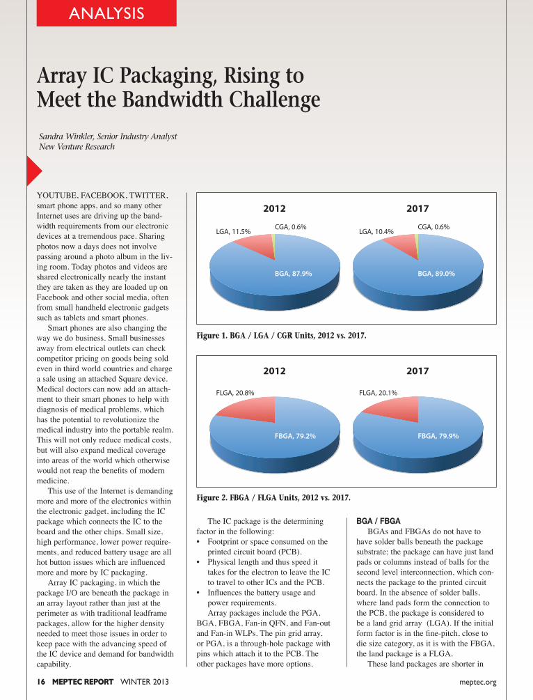
16 MEPTEC REPORT WINTER 2013 meptec.org
ANALYSIS
Array IC Packaging, Rising to Meet the Bandwidth Challenge Sandra Winkler, Senior Industry Analyst New Venture Research
YOUTUBE, FACEBOOK, TWITTER, smart phone apps, and so many other Internet uses are driving up the band-width requirements from our electronic devices at a tremendous pace. Sharing photos now a days does not involve passing around a photo album in the liv-ing room. Today photos and videos are shared electronically nearly the instant they are taken as they are loaded up on Facebook and other social media, often from small handheld electronic gadgets such as tablets and smart phones. Smart phones are also changing the way we do business. Small businesses away from electrical outlets can check competitor pricing on goods being sold even in third world countries and charge a sale using an attached Square device. Medical doctors can now add an attach-ment to their smart phones to help with diagnosis of medical problems, which has the potential to revolutionize the medical industry into the portable realm. This will not only reduce medical costs, but will also expand medical coverage into areas of the world which otherwise would not reap the benefits of modern medicine. This use of the Internet is demanding more and more of the electronics within the electronic gadget, including the IC package which connects the IC to the board and the other chips. Small size, high performance, lower power require-ments, and reduced battery usage are all hot button issues which are influenced more and more by IC packaging. Array IC packaging, in which the package I/O are beneath the package in an array layout rather than just at the perimeter as with traditional leadframe packages, allow for the higher density needed to meet those issues in order to keep pace with the advancing speed of the IC device and demand for bandwidth capability.
The IC package is the determining factor in the following:• Footprint or space consumed on the printed circuit board (PCB).• Physical length and thus speed it takes for the electron to leave the IC to travel to other ICs and the PCB.• Influences the battery usage and power requirements. Array packages include the PGA, BGA, FBGA, Fan-in QFN, and Fan-out and Fan-in WLPs. The pin grid array, or PGA, is a through-hole package with pins which attach it to the PCB. The other packages have more options.
BGA / FBGA BGAs and FBGAs do not have to have solder balls beneath the package substrate; the package can have just land pads or columns instead of balls for the second level interconnection, which con-nects the package to the printed circuit board. In the absence of solder balls, where land pads form the connection to the PCB, the package is considered to be a land grid array (LGA). If the initial form factor is in the fine-pitch, close to die size category, as it is with the FBGA, the land package is a FLGA. These land packages are shorter in
Figure 1. BGA / LGA / CGR Units, 2012 vs. 2017.
2012 2017
CGA, 0.6%LGA, 11.5%
BGA, 87.9%
CGA, 0.6%LGA, 10.4%
BGA, 89.0%
Figure 2. FBGA / FLGA Units, 2012 vs. 2017.
2012 2017
FLGA, 20.8%
FBGA, 79.2%
FLGA, 20.1%
FBGA, 79.9%
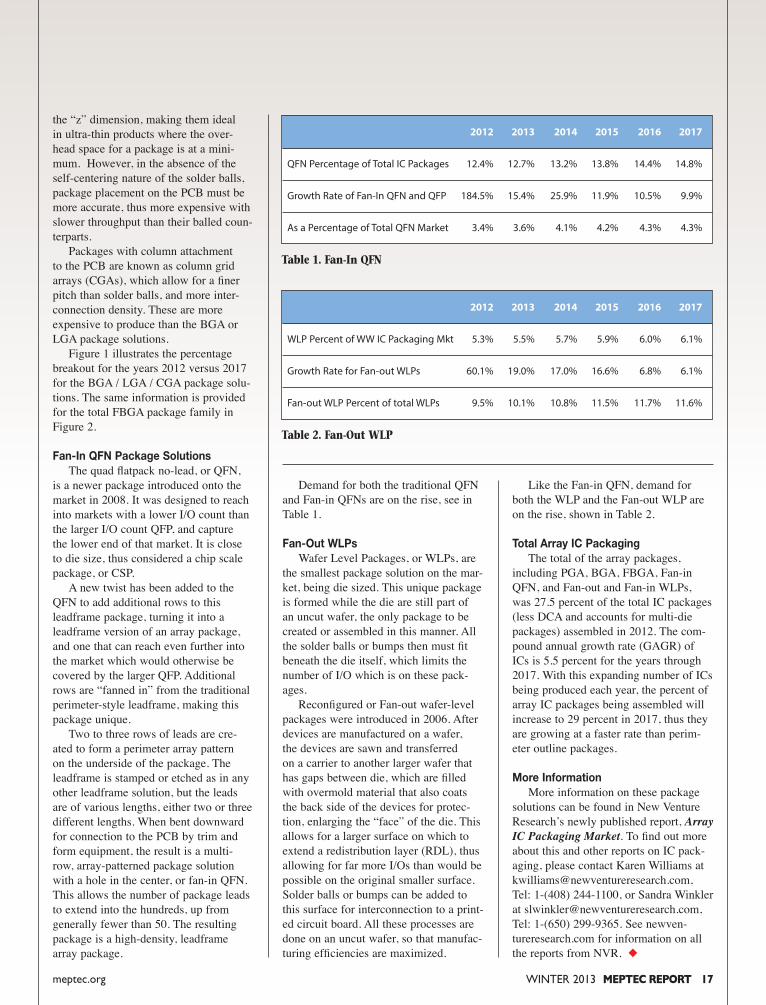
WINTER 2013 MEPTEC REPORT 17meptec.org
the “z” dimension, making them ideal in ultra-thin products where the over-head space for a package is at a mini-mum. However, in the absence of the self-centering nature of the solder balls, package placement on the PCB must be more accurate, thus more expensive with slower throughput than their balled coun-terparts. Packages with column attachment to the PCB are known as column grid arrays (CGAs), which allow for a finer pitch than solder balls, and more inter-connection density. These are more expensive to produce than the BGA or LGA package solutions. Figure 1 illustrates the percentage breakout for the years 2012 versus 2017 for the BGA / LGA / CGA package solu-tions. The same information is provided for the total FBGA package family in Figure 2.
Fan-In QFN Package Solutions The quad flatpack no-lead, or QFN, is a newer package introduced onto the market in 2008. It was designed to reach into markets with a lower I/O count than the larger I/O count QFP, and capture the lower end of that market. It is close to die size, thus considered a chip scale package, or CSP. A new twist has been added to the QFN to add additional rows to this leadframe package, turning it into a leadframe version of an array package, and one that can reach even further into the market which would otherwise be covered by the larger QFP. Additional rows are “fanned in” from the traditional perimeter-style leadframe, making this package unique. Two to three rows of leads are cre-ated to form a perimeter array pattern on the underside of the package. The leadframe is stamped or etched as in any other leadframe solution, but the leads are of various lengths, either two or three different lengths. When bent downward for connection to the PCB by trim and form equipment, the result is a multi-row, array-patterned package solution with a hole in the center, or fan-in QFN. This allows the number of package leads to extend into the hundreds, up from generally fewer than 50. The resulting package is a high-density, leadframe array package.
Like the Fan-in QFN, demand for both the WLP and the Fan-out WLP are on the rise, shown in Table 2.
Total Array IC Packaging The total of the array packages, including PGA, BGA, FBGA, Fan-in QFN, and Fan-out and Fan-in WLPs, was 27.5 percent of the total IC packages (less DCA and accounts for multi-die packages) assembled in 2012. The com-pound annual growth rate (GAGR) of ICs is 5.5 percent for the years through 2017. With this expanding number of ICs being produced each year, the percent of array IC packages being assembled will increase to 29 percent in 2017, thus they are growing at a faster rate than perim-eter outline packages.
More Information More information on these package solutions can be found in New Venture Research’s newly published report, Array IC Packaging Market. To find out more about this and other reports on IC pack-aging, please contact Karen Williams at [email protected], Tel: 1-(408) 244-1100, or Sandra Winkler at [email protected], Tel: 1-(650) 299-9365. See newven-tureresearch.com for information on all the reports from NVR. ◆
Demand for both the traditional QFN and Fan-in QFNs are on the rise, see in Table 1.
Fan-Out WLPs Wafer Level Packages, or WLPs, are the smallest package solution on the mar-ket, being die sized. This unique package is formed while the die are still part of an uncut wafer, the only package to be created or assembled in this manner. All the solder balls or bumps then must fit beneath the die itself, which limits the number of I/O which is on these pack-ages. Reconfigured or Fan-out wafer-level packages were introduced in 2006. After devices are manufactured on a wafer, the devices are sawn and transferred on a carrier to another larger wafer that has gaps between die, which are filled with overmold material that also coats the back side of the devices for protec-tion, enlarging the “face” of the die. This allows for a larger surface on which to extend a redistribution layer (RDL), thus allowing for far more I/Os than would be possible on the original smaller surface. Solder balls or bumps can be added to this surface for interconnection to a print-ed circuit board. All these processes are done on an uncut wafer, so that manufac-turing efficiencies are maximized.
2012 2013 2014 2015 2016 2017
QFN Percentage of Total IC Packages 12.4% 12.7% 13.2% 13.8% 14.4% 14.8%
Growth Rate of Fan-In QFN and QFP 184.5% 15.4% 25.9% 11.9% 10.5% 9.9%
As a Percentage of Total QFN Market 3.4% 3.6% 4.1% 4.2% 4.3% 4.3%
Table 1. Fan-In QFN
2012 2013 2014 2015 2016 2017
WLP Percent of WW IC Packaging Mkt 5.3% 5.5% 5.7% 5.9% 6.0% 6.1%
Growth Rate for Fan-out WLPs 60.1% 19.0% 17.0% 16.6% 6.8% 6.1%
Fan-out WLP Percent of total WLPs 9.5% 10.1% 10.8% 11.5% 11.7% 11.6%
Table 2. Fan-Out WLP
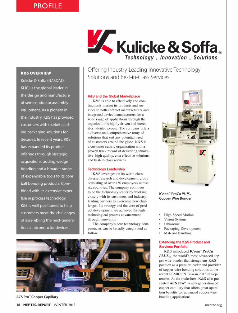
K&S and the Global Marketplace K&S is able to effectively and con-tinuously market its products and ser-vices to both contract manufacturers and integrated device manufacturers for a wide range of applications through the organization’s highly driven and incred-ibly talented people. The company offers a diverse and comprehensive array of solutions that suit any potential need of customers around the globe. K&S is a customer centric organization with a proven track record of delivering innova-tive, high quality, cost effective solutions, and best-in-class services.
Technology Leadership K&S leverages on its world class diverse research and development group consisting of over 450 employees across six countries. The company continues to be the technology leader by working closely with its customers and industry-leading partners to overcome new chal-lenges. Its strategy and the core of prod-uct development are achieved through technological process advancement through innovation. The company’s core technology com-petencies can be broadly categorized as follow:
• High Speed Motion• Vision System• Ultrasonic• Packaging Development• Material Handling
Extending the K&S Product and Services Portfolio K&S introduced IConnPS ProCu PLUSTM, the world’s most advanced cop-per wire bonder that strengthens K&S’ position as a premier leader and provider of copper wire bonding solutions at the recent SEMICON Taiwan 2013 in Sep-tember. At the tradeshow, K&S also pre-sented ACS ProTM, a new generation of copper capillary that offers great opera-tion benefits for advanced copper wire bonding applications.
PROFILE
18 MEPTEC REPORT WINTER 2013 meptec.org
K&S OVERVIEW
Kulicke & Soffa (NASDAQ:
KLIC) is the global leader in
the design and manufacture
of semiconductor assembly
equipment. As a pioneer in
the industry, K&S has provided
customers with market lead-
ing packaging solutions for
decades. In recent years, K&S
has expanded its product
offerings through strategic
acquisitions, adding wedge
bonding and a broader range
of expendable tools to its core
ball bonding products. Com-
bined with its extensive exper-
tise in process technology,
K&S is well positioned to help
customers meet the challenges
of assembling the next-genera-
tion semiconductor devices.
ACS Pro™ Copper Capillary
Offering Industry-Leading Innovative Technology Solutions and Best-in-Class Services
IConn
PS ProCu PLUSTM
Copper Wire Bonder
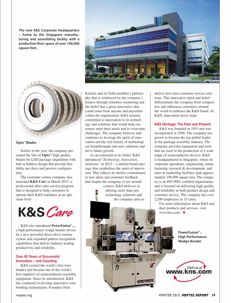
deliver first-class customer service solu-tions. This innovative spirit and belief differentiates the company from competi-tors and influences customers around the world to embrace the K&S brand. At K&S, innovation never stops.
K&S Heritage: The Past and Present K&S was founded in 1951 and was incorporated in 1956. The company has grown to become the top global leader in the package assembly industry. The company provides equipment and tools that are used in the production of a wide range of semiconductor devices. K&S is headquartered in Singapore, where its corporate operations, engineering, manu-facturing, research & development, and sales & marketing facilities span approx-imately 198,000 square feet. The compa-ny is an ISO 9001 certified organization, and is focused on delivering high quality and reliability in both product design and customer service. The company has over 2,200 employees in 15 cities.
For more information about K&S and their products and services, visit www.kns.com. ◆
Kulicke and Al Soffa instilled a philoso-phy that is reinforced by the company’s leaders through relentless mentoring and the belief that a great innovative idea could come from anyone and anywhere within the organization. K&S remains committed to innovation in its technol-ogy and solutions that would help cus-tomers meet their needs and to overcome challenges. The company believes and continues to leverage the spirit of inno-vation and the rich history of technologi-cal breakthroughs into new solutions and drive future growth. As an extension to its belief, K&S introduced “Technology. Innovation. Solutions” in 2013 – a unified brand mes-sage that symbolizes the spirit of innova-tion. This reflects its tireless commitment to new ideas and customer feedback that inspire the company to see around
corners. K&S believes in offering more than just technology solutions and
the company aims to
Earlier in the year, the company pre-sented the line of OptoTM high quality blades for LED package singulation with hub or hubless design that provide flex-ibility per dicer and process configura-tion. The customer centric company also launched K&S Care in March 2013, a professional after sales service program that is designed to help customers to operate their K&S machines at an opti-mum level.
K&S also introduced PowerFusionPSTM,
a high performance wedge bonder driven by a new powerful direct-drive motion system and expanded pattern recognition capabilities that deliver industry leading productivity and reliability.
Over 60 Years of Successful Innovation – and Counting K&S created the world’s first wire bonder and became one of the world’s first suppliers of semiconductor assembly equipment. Since its introduction, K&S has continued to develop innovative wire bonding technologies. Founders Fred
The new K&S Corporate Headquarters – home to the Singapore manufac-turing and assembling facility with a production floor space of over 100,000 square feet.
PowerFusion
PSTM
High Performance Wedge Bonder
WINTER 2013 MEPTEC REPORT 19meptec.org
Opto™ Blades

www.biosensors2014.com REGISTER NOW
C O N F E R E N C E
2014 BIOSENSORS& ANALYTICS
Sensing the Future of Health CareAPRIL 23 & 24, 2014John A. Spitzer Conference CenterLorain County Community CollegeCleveland, Ohio
CONFERENCE TOPICS
Health and Fitness – Sports MedicineThis session will discuss the current MEMS sensor technologies, their current product applications, how they relate to new clinical opportunities, and the biggest challenges that need to be addressed with the emerging opportunities.
Home Health Care – Enabling Extended Patient CareIn this session, potential solutions to home health care/extended patient care challenges will be discussed, including new roles for the patient as well as opportunities for new MEMS sensors and data management strategies.
Metabolic Syndrome – Advancements in Sensors and AnalyticsThis session will cover the advances in sensor technology and metabolic analyzers that complement the direction towards defining each individual’s metabolic signature, the analysis of which can refine fitness management.
Sensors for Hospital Care – Improvements for Patient CareThe use of sensors, actuators and wireless technologies is transforming the modern hospital as well as the detection and treatment of disease in other clinical settings. This session will focus on the impact of new technologies on physician and nurse workflows and decision-making, as well as on patients.
LEARN ABOUT
• Insights from physicians that highlight clinical needs and how devices can address those needs• New MEMS and sensor technologies that can be utilized for healthcare applications • Commercialization assessment of new medical products that utilize MEMS sensors• Strategies for managing regulatory requirements, intellectual property, reimbursement, and adoption
EXHIBITING AND SPONSORSHIP OPPORTUNITIES AVAILABLEContact Bette Cooper at [email protected] for more information
Media Partners
Association Partners
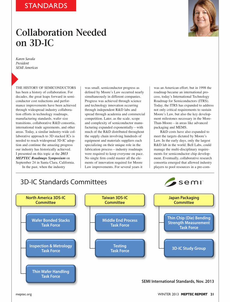
STANDARDS
Collaboration Needed on 3D-IC
WINTER 2013 MEPTEC REPORT 21meptec.org
was an American effort, but in 1998 the roadmap became an international pro-cess, today’s International Technology Roadmap for Semiconductors (ITRS). Today, the ITRS has expanded to address not only critical requirements to sustain Moore’s Law, but also the key develop-ment milestones necessary in the More-Than-Moore—in areas like advanced packaging and MEMS. R&D costs have also expanded to meet the targets dictated by Moore’s Law. In the early days, only the largest R&D lab in the world, Bell Labs, could manage the multi-disciplinary require-ments for semiconductor chip develop-ment. Eventually, collaborative research consortia emerged that allowed industry players to pool resources in a pre-com-
was small, semiconductor progress as defined by Moore’s Law occurred nearly simultaneously in different companies. Progress was achieved through science and technology innovation occurring through independent R&D labs and spread through academia and commercial competition. Later, as the scale, scope and complexity of semiconductor manu-facturing expanded exponentially—with much of the R&D distributed throughout the supply chain involving hundreds of equipment and materials suppliers each specializing on their unique role in the fabrication process—industry roadmaps were required to keep everyone on pace. No single firm could master all the ele-ments of innovation required for Moore Law improvements. For several years it
THE HISTORY OF SEMICONDUCTORS has been a history of collaboration. For decades, the great leaps forward in semi-conductor cost reductions and perfor-mance improvements have been achieved through widespread industry collabora-tion efforts in technology roadmaps, manufacturing standards, wafer size transitions, collaborative R&D consortia, international trade agreements, and other areas. Today, a similar industry-wide col-laborative approach to 3D stacked ICs is needed to reach widespread 3D-IC adop-tion and continue the amazing progress our industry has historically achieved. I presented on this topic at the 2013 MEPTEC Roadmaps Symposium on September 24 in Santa Clara, California. In the past, when the industry
Karen SavalaPresidentSEMI Americas
3D-IC Standards Committees
Thin Chip (Die) BendingStrength Measurement
Task Force
3D-IC Study Group
Middle End ProcessTask Force
TestingTask Force
Wafer Bonded StacksTask Force
Inspection & MetrologyTask Force
Thin Wafer HandlingTask Force
North America 3DS-ICCommittee
Taiwan 3DS-ICCommittee
Japan PackagingCommittee
SEMI International Standards, Nov. 2013
22 MEPTEC REPORT WINTER 2013 meptec.org
STANDARDS
For heterogeneous integration of memory and logic, the industry still needs design tools, thermal solutions, continued work on wafer bonding and de-bonding, and accepted test methodologies, to name a few requirements. Gartner estimates that TSV adoption for memory will be pushed out to 2014 or 2015, with non-memory applications delayed to 2016-17 if that. They cur-rently forecast that TSV devices will account for less five percent of the units in the total wafer-level packaging market by 2017. For 3D-IC to be widely adopted, meaningful collaboration throughout the value chain still needs to occur. At this time in the market, all the important players in the ecosystem have a differ-ent perspective. All the players have a business model that must be defended or exploited based on what technical dis-coveries occur and what customers even-tually want. TSMC sees an integrated approach that threatens the traditional Fabless/Foundry/OSAT model. Obvi-ously leading OSATs prefer this vision as it provides an opportunity to expand their business. But OSATs themselves are looking at ways to differentiate. IDMs like Intel probably see the fabless model coming full circle with 3D IC. Fabless companies believe that 3D must emerge in ways that continue their own—and their customer’s — familiar multiple-sourcing considerations. We’ll continue to see discoveries, inventions and new products in 3D-IC and progress will continue. Hundreds of patents in the area have already been issued. We’re seeing innovation and invention in wafer bonding, via manufac-turing, and other areas. Standards work at JEDEC and SEMI will also contribute to the market’s development, both to enable processes and cost-reduce manu-facturing, but without the emergence of a new, robust collaboration model that can deliver meaningful agreements between key constituencies, the promise of 3D innovation will remain distant and illu-sive. For information on SEMI, visit www.semi.org; for information on SEMI International Standards, visit www.semi.org/en/Standards. ◆
Consortium (G450C) to manage 450mm wafer processing requirements. Recently, G450C set up a separate fab facility consortium. Europe has launched five separate 450mm projects or consortiums, with two others on the drawing board. Israel has established 450mm consortium on metrology and Japan has collaborative arrangement on 450mm with Toshiba. With uncertainties on 450 wafer processing, EUV lithography, and the continued transition to new transistor architectures, many experts are question-ing the continuation of Moore’s Law. It’s been reported that cost targets at 28 nanometers were not reached, 20 nano-meters may be delayed and also come in at a high price. Consequently, the industry has been excited about More-than-Moore applications, especially 3D stacked ICs that promise to improve bandwidth, reduce footprint, decrease power consumption, and lower cost. We have seen the proliferation of stacked die with wire bond or flip chip, stacked packages, package-on-package, and chip-on-chip packages. But today, the most anticipated innovation is 2.5 and 3D stacked ICs using TSVs to achieve both the power and bandwidth benefits associated with a radical new interconnect solution. Like 450mm wafer processing, critical standards foundation work for the adoption 3D-IC is well underway. At SEMI, Standards task forces have been established in thin wafer handling, inspection and metrology, and wafer bonding. But like 450mm wafer process-ing, enabling the 3D-IC revolution will require more than industry standards activities. While a promising technology, technical challenges remain with 3D stacked ICs. Many companies have a silicon interposer or 2.5D solution on their packaging roadmaps where a logic device is mounted next to a stack of memory and the TSVs are in the substrate. However, while Samsung and others have made announcements, affordable stacked memory is not yet available. In addition, many companies are also looking at alternatives to silicon interposers, such as glass interposers, to bring the price down. So, even 2.5D has been delayed and questions remain about its configuration at high volume.
petitive environment to develop the sci-ence and technology needed for the next generation chip. In addition to collaborative road-maps and R&D, the semiconductor industry also agreed upon collective industry standards that reduced cost and spur innovation. These standards involve such areas as wafer size and dimensions, software and hardware interfaces, materi-als characterization and test methods, and hundreds of other areas. Today, there are nearly 4,000 volunteers from every major company working together on SEMI industry standards. They have produced hundreds of widely-accepted standards that have reduced costs and allowed companies to compete on innovation. In addition to SEMI Standards, other stan-dards bodies have emerged such as IEEE and JEDEC to address semiconductor standards needs in electrical, signaling, form factor, packaging and other areas. With roadmaps, standards and consortia in place, the semiconductor industry targeted what was considered by some an “easy” wafer transition to 300mm silicon. It was anything but easy. As many of you know, the transi-tion went poorly. The industry couldn’t agree when to introduce 300mm produc-tion and stop advanced development at 200mm, and they couldn’t afford to do both. There were several false starts and hundreds of millions of dollars were lost. Today, the industry is planning a 450mm wafer transition while at the same time trying to manage the increas-ingly complex R&D challenges of new materials development, new transistor architectures, and new packaging para-digms. The cost of advanced semicon-ductor development has skyrocketed. The industry has responded by dramati-cally expanding the Consortia model for collaborative R&D. Over the last two years, the industry has launched nearly a dozen consortium-like entities in 450mm and related areas of development. Joining Belgium’s imec, Germany’s Fraunhofer Institute, Taiwan’s ITRI, and France’s CEA-Leti — to name a few — are a number of new consortia established to collaborate on joint R&D for 450mm wafers and other next-gen-eration semiconductor challenges. GLO-BALFOUNDRIES, Intel, IBM, Samsung and TSMC formed the Global 450
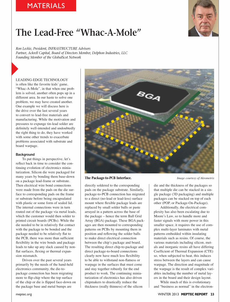
MATERIALS
The Lead-Free “Whac-A-Mole”
WINTER 2013 MEPTEC REPORT 23meptec.org
die and the thickness of the packages so that multiple die can be stacked in a sin-gle package (3D packaging) and multiple packages can be stacked on top of each other (POP, or Package-On-Package). Additionally, the electrical com-plexity has also been escalating due to Moore’s Law, so to handle more and faster signals with more power in this smaller space, it requires the use of com-plex multi-layer laminates with metal patterns embedded within insulating materials such as resins. Of course, the various materials including silicon, met-als and inorganic resins all have differing Coefficient of Thermal Expansion (CTE) so, when subjected to heat, this induces stress between the layers and can cause warpage. The direction and magnitude of the warpage is the result of complex vari-ables including the number of metal lay-ers in the board and their design layout. While much of this is evolutionary and “business as normal” in the electron-
directly soldered to the corresponding pads on the package substrate. Similarly, package-to-PCB connection has migrated to a direct (no-lead or lead-less) surface mount where flexible package leads are replaced by small solder balls or paste arrayed in a pattern across the base of the package – hence the term Ball Grid Array (BGA) package. These BGA pack-ages are then mounted to corresponding patterns on PCBs by mounting them in position and reflowing the solder balls to make direct electrical connection between the chip’s package and board. The resulting direct chip-to-package and direct package-to-board connections clearly now have much less flexibility to be able to withstand non-flatness or warpage in the surfaces that must come and stay together robustly for the end product to work. The continuing minia-turization of electronics has also driven chipmakers to drastically reduce the thickness (really thinness) of the silicon
LEADING-EDGE TECHNOLOGY is often like the favorite kids’ game, “Whac-A-Mole”, in that when one prob-lem is solved, another often pops up in a different area. In our haste to solve one problem, we may have created another. One example we will discuss here is the drive over the last several years to convert to lead-free materials and manufacturing. While the motivation and pressures to expunge tin-lead solder are definitely well-intended and undoubtedly the right thing to do, they have worked with some other trends to exacerbate problems associated with substrate and board warpage.
Background To put things in perspective, let’s reflect back in time to consider the con-tinuing evolution of electronics minia-turization. Silicon die were packaged for many years by bonding them base-down on a package lead-frame or substrate. Then electrical wire bond connections were made from the pads on the die sur-face to corresponding pads on the frame or substrate before being encapsulated with plastic or some form of sealed lid. The internal connections were in turn routed out of the package via metal leads, which the customer would then solder to printed circuit boards (PCBs). While the die needed to be in relatively flat contact with the package to be bonded and the package needed to be relatively flat to the PCB, there was more than sufficient flexibility in the wire bonds and package leads to take up any slack caused by non-flat surfaces, flexing or thermal expan-sion mismatch. Driven over the past several years primarily by the needs of the hand-held electronics community, the die-to-package connection has been migrating more to flip-chip where the top surface of the chip or die is flipped face-down on the package base and metal bumps are
Ron Leckie, President, INFRASTRUCTURE AdvisorsPartner, Ackrell Capital, Board of Directors Member, Delphon Industries, LLC Founding Member of the GlobalScot Network
The Package-to-PCB Interface. Image courtesy of Akrometrix
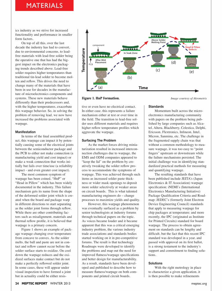
24 MEPTEC REPORT WINTER 2013 meptec.org
MATERIALS
Standards Momentum built across the micro-electronics manufacturing community with papers on the problem being pub-lished by large companies such as Alca-tel, Altera, Blackberry, Celestica, Delphi, Ericsson, Flextronics, Infineon, Intel, Micron, Sanmina, etc. The challenge in the fragmented supply chain was that without a common methodology to mea-sure warpage, it was too easy to “point fingers” upstream or downstream while the failure mechanisms persisted. The initial challenge was in identifying stan-dardized practical methods for measuring and quantifying warpage. The resulting standards that have been published include JEITA’s (Japan Electronics & IT Association) warpage specification; iNEMI’s (International Electronics Manufacturing Initiative) Package Qualification Criteria and Road-map; JEDEC’s (formerly Joint Electron Device Engineering Council) standards that apply to measuring warpage for chip packages at temperature; and more recently, the IPC (originated as Institute for Printed Circuits) standard for board warpage. The process to obtain agree-ment on standards can be lengthy and difficult, but the fact that this recent IPC standard was developed in a year, and passed with approval on its first ballot, is a strong testament to the industry’s support and commitment to finding solu-tions.
Solutions With the right metrology in place to characterize a given application, it is then possible to make refinements
tive or even have no electrical contact. In either case, this represents a failure mechanism either at test or over time in the field. The transition to lead-free sol-der uses different materials and requires higher reflow temperature profiles which aggravate the warpage.
Surfacing The Problem As the market forces driving minia-turization resulted in increased intercon-nection challenges due to warpage, the EMS and ODM companies appeared to “keep the lid” on the problem by cre-atively tweaking the solder reflow pro-cess to accommodate the symptoms of warpage. This was achieved through such items as increased solder paste thick-ness or wider mask openings to deposit more solder selectively at weaker areas on circuit boards. This is what talented manufacturing engineers do – change processes to maximize yields and quality. However, this warpage phenomenon was eventually surfaced as a problem by senior technologists at industry forums through technical papers on the topic. As voices became louder and it became apparent that this was a critical emerging industry problem, the various industry trade associations and standards bodies started working on it in pre-competitive forums. The result is that technology Roadmaps were developed to identify the problems and map out the need for improved flatness/warpage specifications and better design for manufacturability. As a result, standards have been devel-oped and published to describe how to measure flatness/warpage on both com-ponents and printed circuit boards.
ics industry as we strive for increased functionality and performance in smaller form factors, On top of all this, over the last decade the industry has had to convert, due to environmental concerns, to lead-free materials with lead-free solder being the operative one that has had the big-gest impact on the electronics packag-ing trends described above. Lead-free solder requires higher temperatures than traditional tin-lead solder to become mol-ten and reflow. This drives the need to change many of the materials that have been in use for decades in the manufac-ture of microelectronics components and systems. These new materials behave differently than their predecessors and, with the higher temperatures, exacerbate this warpage behavior. So, in solving the problem of removing lead, we now have increased the problems associated with warpage.
Manifestation In terms of the final assembled prod-uct, this warpage can impact it by poten-tially causing some of the electrical joints between the semiconductor package and the PCB to either not make connection (a manufacturing yield and cost impact) or make a weak connection that works ini-tially but fails over time/use (a reliability impact - and even greater cost impact). The most common symptom of warpage has been coined, “HnP” or “Head in Pillow” which has been widely documented in the industry. This failure mechanism gets its name from the shape of the deformed solder joint which is cre-ated when the board and package warp in different directions to start separating as the solder joint forms through reflow. While there are other contributing fac-tors such as misalignment, materials and thermal reflow profile, it is believed that warpage is a primary concern. Figure 1 shows an example of pack-age warpage changing over temperature from concave to convex. As the solder melts, the ball and paste are not in con-tact and reflow cannot occur before the solder surface starts to oxidize. On cool down the warpage reduces and the oxi-dized surfaces make contact but do not make a perfectly reflowed solder joint. In some cases, these will appear under visual inspection to have formed a joint but in actuality could be either resis-
Figure 1. HnP Formation. Image courtesy of Akrometrix
After BGA Placement
Tem
pera
ture
Time
component
PCB
(a)
(b)
(c)
(d)
(e)
In Soak Zone
Above SolderMelting Point
Head & PillowDefects
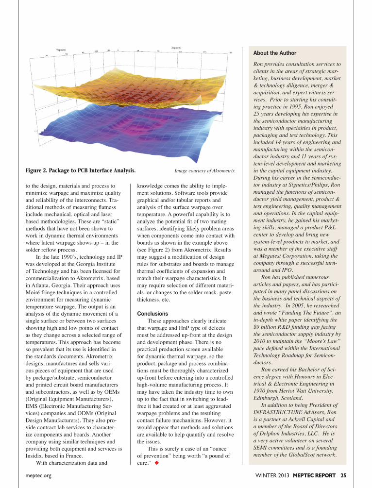
to the design, materials and process to minimize warpage and maximize quality and reliability of the interconnects. Tra-ditional methods of measuring flatness include mechanical, optical and laser based methodologies. These are “static” methods that have not been shown to work in dynamic thermal environments where latent warpage shows up – in the solder reflow process. In the late 1990’s, technology and IP was developed at the Georgia Institute of Technology and has been licensed for commercialization to Akrometrix, based in Atlanta, Georgia. Their approach uses Moiré fringe techniques in a controlled environment for measuring dynamic temperature warpage. The output is an analysis of the dynamic movement of a single surface or between two surfaces showing high and low points of contact as they change across a selected range of temperatures. This approach has become so prevalent that its use is identified in the standards documents. Akrometrix designs, manufactures and sells vari-ous pieces of equipment that are used by package/substrate, semiconductor and printed circuit board manufacturers and subcontractors, as well as by OEMs (Original Equipment Manufacturers), EMS (Electronic Manufacturing Ser-vices) companies and ODMs (Original Design Manufacturers). They also pro-vide contract lab services to character-ize components and boards. Another company using similar techniques and providing both equipment and services is Insidix, based in France. With characterization data and
WINTER 2013 MEPTEC REPORT 25meptec.org
knowledge comes the ability to imple-ment solutions. Software tools provide graphical and/or tabular reports and analysis of the surface warpage over temperature. A powerful capability is to analyze the potential fit of two mating surfaces, identifying likely problem areas when components come into contact with boards as shown in the example above (see Figure 2) from Akrometrix. Results may suggest a modification of design rules for substrates and boards to manage thermal coefficients of expansion and match their warpage characteristics. It may require selection of different materi-als, or changes to the solder mask, paste thickness, etc.
Conclusions These approaches clearly indicate that warpage and HnP type of defects must be addressed up-front at the design and development phase. There is no practical production screen available for dynamic thermal warpage, so the product, package and process combina-tions must be thoroughly characterized up-front before entering into a controlled high-volume manufacturing process. It may have taken the industry time to own up to the fact that in switching to lead-free it had created or at least aggravated warpage problems and the resulting contact failure mechanisms. However, it would appear that methods and solutions are available to help quantify and resolve the issues. This is surely a case of an “ounce of prevention” being worth “a pound of cure.” ◆
About the Author
Ron provides consultation services to clients in the areas of strategic mar-keting, business development, market & technology diligence, merger & acquisition, and expert witness ser-vices. Prior to starting his consult-ing practice in 1995, Ron enjoyed 25 years developing his expertise in the semiconductor manufacturing industry with specialties in product, packaging and test technology. This included 14 years of engineering and manufacturing within the semicon-ductor industry and 11 years of sys-tem-level development and marketing in the capital equipment industry. During his career in the semiconduc-tor industry at Signetics/Philips, Ron managed the functions of semicon-ductor yield management, product & test engineering, quality management and operations. In the capital equip-ment industry, he gained his market-ing skills, managed a product P&L center to develop and bring new system-level products to market, and was a member of the executive staff at Megatest Corporation, taking the company through a successful turn-around and IPO. Ron has published numerous articles and papers, and has partici-pated in many panel discussions on the business and technical aspects of the industry. In 2005, he researched and wrote “Funding The Future”, an in-depth white paper identifying the $9 billion R&D funding gap facing the semiconductor supply industry by 2010 to maintain the “Moore’s Law” pace defined within the International Technology Roadmap for Semicon-ductors. Ron earned his Bachelor of Sci-ence degree with Honours in Elec-trical & Electronic Engineering in 1970 from Heriot Watt University, Edinburgh, Scotland. In addition to being President of INFRASTRUCTURE Advisors, Ron is a partner at Ackrell Capital and a member of the Board of Directors of Delphon Industries, LLC. He is a very active volunteer on several SEMI committees and is a founding member of the GlobalScot network.
Figure 2. Package to PCB Interface Analysis. Image courtesy of Akrometrix

AS WE NEAR THE END OF 2013, THE stability many were hoping would take shape this year hasn’t materialized; the global electronics industry continues to be affected by uncertain economic con-ditions, with many sectors and regions experiencing very challenging climates. Despite this, however, several technology applications continue to advance and, in some markets, there is notable growth occurring and next-generation product designs continuing unabated. Understand-ing underlying market requirements well ahead of implementation is fundamental to Henkel’s materials development success. That’s not to say our customers haven’t been affected by the current situation – they have – but the fortitude and foresight to see beyond today’s challenges and into tomorrow’s opportunities is what makes our company and customers different. Innovation is a deliberate process within Henkel, with dedicated teams focused on progressing future chemistries that will be integral to development of transforma-tional products and capabilities in many markets including handhelds, automotive, medical and industrial, among others. In 2013, Henkel delivered on several fronts, launching multiple materials for various markets, most notably in the handheld and automotive sectors. Without question, handheld devices are driving much of the electronics industry’s growth. In fact, smartphone unit sales unsurprisingly continue to outpace sales of PCs and, perhaps more notable is that tablets will soon surpass PC shipments as well. According to Business Insider, tablet sales will reach 500 million units by 2015, up from 95 million in 2011.(1) Key to this growth is consumer expecta-tions: consumers demand that their mobile products perform well, stay cool despite increasing density and functionality, survive multiple drops and challenging
difference between success and failure, having a complete portfolio of proven MEMS packaging materials is a tremen-dous advantage and one where Henkel is unmatched. This, in addition to a broad materials range for the assembly of cam-era modules, makes Henkel the leading supplier of materials for future, higher functioning handheld devices. And lastly, Henkel has been the first to introduce a variety of novel semiconductor packaging materials which enable the miniaturiza-tion of components for the consumer market, such as pre-applied and dispensed underfill for use with fine-pitch applica-tion processors and modems, and conduc-tive die attach film for RF modules and power ICs. Automotive electronics is another growth sector within the broader elec-tronics industry and a market where Henkel has considerable experience and a strong innovation delivery track record. Advanced automotive electron-ics applications are projected to grow at an astonishing 50% in the 2010 to 2020 decade, according to IMS Research, and reach a value of $240 billion.(2) This, of course, is a large category and covers everything from in-cabin entertainment to lighting to safety features and more. As auto manufacturers integrate more electronic function into vehicles, address-ing concerns such as managing higher temperatures and vibration, as well as ensuring uncompromising reliability, are at the forefront of new auto device devel-opment. Henkel’s decades of innovation success in automotive electronics contin-ues into the evolution of vehicle features, with novel materials that are helping auto manufacturers cope with new demands. A novel approach to electrically conductive adhesives (ECAs) has leveraged silicone’s
environments and continue to offer even more features. It’s no small task to project future materials needs – let alone keep up with the current requirements – but that is exactly what Henkel has consistently done since the launch of the first smartphone in 2007. Over the last year alone, several of Henkel’s priority materials develop-ment projects for handhelds have come to market ahead of schedule. Novel thermal absorbent films that help lower CPU and skin temperature now give handheld manufacturers a solution that is contour-able and adaptable to tight geometries. This offers welcome design leverage over more rigid materials like graphite, while also delivering a measurable improvement in temperature reduction. New chemistry approaches have also resulted in the for-mulation of a versatile underfill material that provides high reliability, but is much easier to rework as compared to previous generation materials. The high Tg of this underfill delivers excellent reliability, but in a highly reworkable formula. This is not an easy balance to strike, but one that Henkel has successfully navigated and is very important for high-value products. Off-the-shelf, market-ready MEMS solu-tions are also critical to the function of today’s handheld products, which can contain as many as 10 MEMS devices each. As time-to-market speed is often the
Intentional Innovation Drives Market SuccessGrowth Markets Require Forward-Looking Solutions
Kevin Becker Henkel Electronic Materials, LLC
26 MEPTEC REPORT WINTER 2013 meptec.org
continued on page 29
Henkel’s Thermal Absorbent Film, Loctite TAF-8800

Henkel Americas: +1 949 789 2500 Henkel Europe: +44 1442 278 000 Henkel Asia: +86 21 2891 8000 www.henkel.com/electronics
For more information contact:
No matter where you are or what your process requires, you can count on Henkel’s expertise. Our unmatched portfolio
of advanced materials for the semiconductor and assembly markets all backed by the innovation, knowledge and support of
Henkel’s world-class global team ensures your success and guarantees a low-risk partnership proposition.
Anticipating your ideas Shows us the way to innovation

®
REGISTER TODAY www.IPCAPEXEXPO.org
DESIGN | PRINTED BOARDS | ELECTRONICS ASSEMBLY | TEST
• TRUST in the expertise of IPC — recognized worldwide as the leading standards organization for electronics manufacturing.
• EXPLORE emerging technologies and the latest innovations that will shape the future of our industry.
• COMPARE equipment, materials and supplies from more than 400 of our industry’s top companies, in one location.
• LEARN about the latest research and processes that will advance your career and your company.
• BE INSPIRED with new ideas and approaches that will turn your vision into tomorrow’s realities.
“ IPC APEX EXPO is the best place to see multiple, various suppliers of equipment all in one place.”
Scott ButtarsOperation ManagerZELPRO Assembly Solutions
CONFERENCE & EXHIBITION > March 25-27, 2014MEETINGS & EDUCATION > March 23-27, 2014MANDALAY BAY RESORT AND CONVENTION CENTERLAS VEGAS, NEVADA
www.IPCAPEXEXPO.org
BOARD LETTER
WINTER 2013 MEPTEC REPORT 29meptec.org
companies take a much more active role in the acquisition and development of their own technologies, offsetting some of the effect of a stronger and more capable semiconductor supplier partner. Thus, some system companies are diving more deeply than ever into how systems are physically assembled, down to the micron level and below.
SiP – A “New” IC Packaging Value Proposition Is there a value proposition in this new era for the IC packaging commu-nity? I believe there is. It has the well-recognized name of SiP, System in Pack-age, but it brings with it capabilities far beyond those even realized a few years back. First off, the core competencies of IC packaging suppliers like ASE are stron-ger than ever. Wafer thinning is being performed to below 50 microns. Wire bonding is being performed at pitches down to 40 microns using Cu instead
capability that can product widely diverse and shrinking form factors within a rela-tively short development time. Compa-nies that can leverage these capabilities toward design and launch of their real life products will find ample opportuni-ties for growth in the future. But when you integrate many die, some from different companies, into an SiP, can you really manage yields? Isn’t this the same problem that stunted the growth of MCM in the 90’s? Times have changed, but yields must be man-aged. Today, billions of IC packages that contain more than one die are produced. Hundreds of millions of those products contain die from different companies. If you go to the right companies for the solutions, business models and capabili-ties exist today to support system and sub-system packaging as described. I am bullish about the future of pack-aging. I believe if players are positioned well, thanks to the ever increasing cost of Moore’s Law, packaging opportuni-ties are alive and well for the foreseeable future, especially in the SiP arena. ◆
of higher cost gold. Flip chip is migrat-ing to the use of Cu pillar bumps which enable higher density and higher perfor-mance than previously with solders. Die attach and underfill materials are rapidly formulated to tune physical properties to the application. Substrates used as integration platforms can range from Cu leadframes, to very capable glass filled or coreless laminates, to polyimide films, and even to interposers made of silicon. Both passive and simple active compo-nents can now be embedded inside PCB structures. Passive components can be rapidly integrated and produced on glass, with the future intent of creating a value added interposer platform. SMT pro-cesses are commonly integrated into IC packages that add additional functionality at reasonable cost. Design and simulation techniques allow designers to optimize many physical and electrical aspects of the package well before it is even made. All of these developments and capa-bilities which reside in the tool boxes of the most advanced packaging companies produce a very flexible manufacturing
continued from page 3
unique properties to manage harsh envi-ronments as electronic sensors move ever closer to the vehicle sources of heat and vibration. These new ECAs have capabil-ity focusing on electrical resistance, adhe-sion, thermal conductivity and flexibility while delivering high temperature and high vibration compatibility. Automotive electronics manufacturers must also com-ply with environmental legislation and uti-lize lead-free solder materials. Traditional Pb-free solders haven’t offered the high reliability required in auto applications, but Henkel’s new solder alloy, 90iSC, delivers SnPb-like performance and reli-ability in a Pb-free formulation and is earning the praises of leading global auto-motive electronics manufacturers. Other innovations in circuit board protection, electrically conductive inks and ther-mal management materials are offering unique, cost-effective and highly reliable approaches to modern vehicle design. At Henkel, our perspective on elec-
on our team’s market and application foresight and expertise. Driving value for our customers is our top objective and is what has made Henkel the world’s leading electronic materials company. ◆
Sources1. http://www.onlinemarketing-trends.com/2012/07/growth-rate-comparison-pc-vs.html#.UopJHv4o7IU
2. http://phys.org/news/2013-05-explosive-growth-automotive-electronics.html
continued from page 26
tronics systems – whether a high-function-ing handheld device, a medical biosensor or a 2016 model vehicle – is holistic. We understand how each element of the device interacts and how those com-ponents work together in a functioning system. This comprehensive view under-pins our innovation culture. At Henkel, innovation doesn’t happen by chance; it’s a deliberate and intentional process based
OPINION
IT IS HARD TO BELIEVE THAT THE semiconductor industry, that’s almost taken for granted today, got its start in only the mid-20th century. In the early 1960’s, an “integrated circuit” with two transistors on a chip was quite an achievement. Intel impressed the industry in the 1970’s by yielding its 4004 with 2300 transistors. Back then, who could have dreamed that 5 BILLION transistor chips would be in mass production less than 50 years later - and that their cost effectiveness would drive them into low-cost consumer products used by the majority of the people on the planet? Throughout the decades, semiconduc-tors have been one of the most dynamic and innovative industries ever known - fueled by advancements in process technology com-bined with technical ingenuity. It has also been unique in that each new generation of technology brought not just new capabili-ties but lower costs. The cost of innovation remained within reach for a vast array of companies and the ecosystem grew to hun-dreds of semiconductor manufacturers sup-ported by thousands of suppliers. With more participants came more innovation and the success cycle repeated over and over. Each time pundits predicted an insurmountable process technology barrier, it was breached. But, as we moved into the 21st century, things began to change. Yes, semiconduc-tor technology continued to move along the Moore's Law curve but the cost of the advances became higher and higher - both in terms of capital equipment and chip NRE. The number of companies who could afford to play began to shrink. In 2012, the five semiconductor companies with the largest capital equipment budgets moved aggres-sively toward 450mm manufacturing, spend-ing 35% of sales on capital equipment while the rest of the industry spent only 10% (source: IC Insights). Leading-edge technol-ogy has become a game for the very largest and wealthiest semiconductor companies. Recognizing this trend, a handful of Inte-grated Device Manufacturers (IDM) joined together almost ten years ago to explore ways to succeed without gargantuan capital equipment budgets and without building the most state-of-the-art geometries. The
parts has been a time and anguish saver for many FOA members.
Personnel Issues Staffing and running a fab represents a unique set of personnel challenges:- How should shifts be organized and what’s the best hand-off procedure?- Work rules for specific equipment- Managing the aging workforce: knowledge transferal and hiring replacements for retirees- Managing permanent vs. temporary employeesValuable insights to these and many other issues can be gained if companies in similar situations dialog and share experiences.
Sharing of Supplier Experiences When a company needs a legacy tool repaired or serviced, the best choice isn’t always clear. Use the OEM tool supplier? Go with a 3rd party provider? It’s extremely useful to know what the experience of similar companies has been and what they recommend.
Supplier Influence As OEM tool suppliers invest in 450mm, they have looked for ways to cut support for legacy tools. Manufacturers using older tools, especially those at 150 and 200mm, can be caught without support if they go it alone but, when a large number band togeth-er, they represent a large enough installed base to command the attention they need from the original tool suppliers.
Access to a Large Number of Suppliers Individual companies don’t always have time to keep current with the supplier base and to know what products and services are available. When a large number of semicon-ductor manufacturers agree to gather in one forum, their suppliers - even relatively small ones - can afford to come to them, listen to their problems and propose solutions. Today, the FOA includes over 25 device manufacturers as well as 70 supplier com-panies. Its tremendous growth since 2004 attests to the value of collaboration within our industry and we believe that such shar-ing will only grow in importance for those chip companies beyond today’s Big Three. ◆
solution lay in what products were built and HOW the IDMs built them. They real-ized that they needed to give up the age-old assumption that everything in their shop was proprietary. In the new reality of the indus-try, this was an unjustifiable expense that could spell the difference between being in the “black” or in the “red”. To paraphrase a famous quote: “If they did not hang togeth-er, they would surely hang separately”. Of the 49 fabs that closed between 2009-2011, the predominant number were at 150mm diameter. One of biggest opportunities for improv-ing the performance and efficiency of such fabs was in Collaboration with their traditional competitors in addressing com-mon issues, while still keeping their “secret sauce” secret. The most obvious area for collaboration was in the manufacturing process itself - process methodology, tool availability, maintenance, supplier issues and training to name just some of the opportuni-ties. Thus, the Fab Owners Association was born. Within the framework of the FOA, companies who, in the past, would never have spoken to each other, dialog about many manufacturing-related issues without compromising their competitive advantage. In fact, collaboration greatly improves their ability to focus their limited resources on areas of true differentiation. Some of the demonstrated successes of collaboration include:
Best Practices in Process Flow Manufacturers get the most out of the legacy tools by sharing insights and “war stories”. Someone else may have a tech-nique for squeezing just a bit more through-put out of a bottleneck tool. And, if you're having a problem, chances are someone else has already seen it.
Legacy Tool Maintenance & Sparing Time spent on maintenance is tool down-time so sharing information about optimal maintenance schedules for older equipment is an important source of fab efficiency. When a tool does go down or becomes erratic, getting it working again is crucial. Having experts at other companies to con-sult with and potentially assist with spare
The Power of Collaboration
30 MEPTEC REPORT WINTER 2013 meptec.org
Joe Ardini, Vice President Fab Owners Association

LGA Power Amp
RF
MLF®
PMICAudio Codec
Power AmplifierTouch Controller
GPS
WLCSP PMIC
Audio CodecPower Amplifier
Compass
Microphone, Pressure, Humidity/Temperature, Gyroscope, Accelerometer, Fingerprint,
Light, Infrared and Fusion Sensors
fcCSP orTMV® PoP
Application ProcessorBasebandMemory
CABGA/FBGAPMIC
Audio CodecBaseband
Camera ModuleRF
SCSPMemory
BasebandRF
FCMBGAGraphic Processor
fcCSPPMIC
Combo Chip
Sensor Packages
Visit Amkor Technology online for the most current product information and locations.
www.amkor.comPackages not shown at actual size. © 2013 Amkor Technology, Inc.
CavityMEMS LGA MLF®
Perfection Products Inc.1320 S. Indianapolis Ave. • Lebanon, IN 46052Phone: (765) 482-7786 • Fax: (765) 482-7792
Check out our Website: www.perfection-products.comEmail: [email protected]
Grip Ring Shippers
I. C. Trays - Multi-Channel
Lead Frame Magazines - F.O.L./E.O.L.
Film Frame Magazines
Film Frames Film Frame Shippers
TO Tapes & Magazines
Magazines and Carriers for Process Handling Solutions
Accept Nothing Less.
Substrate Carrier Magazines
Stack Magazines - E.O.L.
Wafer Carriers
Process Carriers (Boats)
Boat Magazines
Grip Rings
Miscellaneous Magazines
I. C. Tubes and Rails
Grip Ring Magazines