micro programmable logic controller - idec
TRANSCRIPT

FC9Y-B927
FC5A SERIES
Micro Programmable Logic Controller
User’s Manual
C
OMPARISON
FC5A M
ICRO
S
MART
U
SER
’
S
M
ANUAL
M
ICRO
S
MART
FC4A
VS
. FC5A
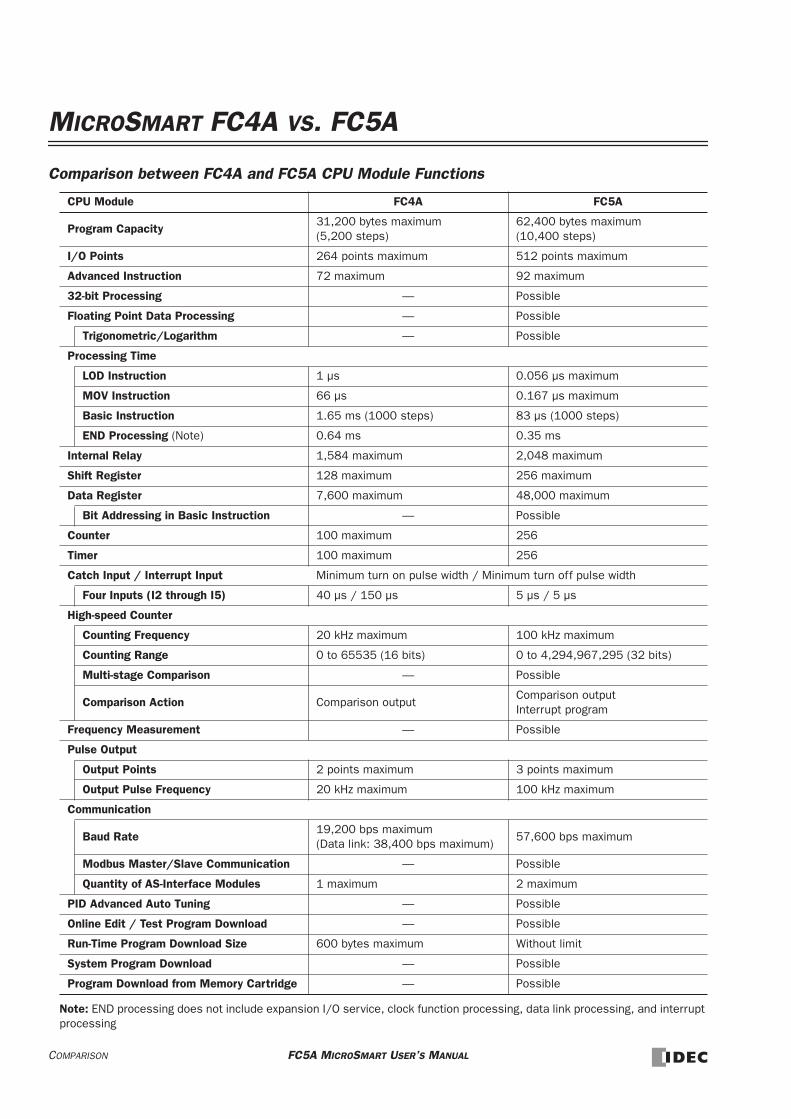
Comparison between FC4A and FC5A CPU Module Functions
Note:
END pr
ocessing does not include expansion I/O ser
vice, clock function pr
ocessing, data link pr
ocessing, and inter
r
upt
pr
ocessing
CPU Module
FC4A
FC5A
Pr
ogram Capacity
31,200 bytes maximum
(5,200 steps)
62,400 bytes maximum
(10,400 steps)
I/O Points
264 points maximum
512 points maximum
Advanced Instr
uction
72 maximum
92 maximum
32-bit Pr
ocessing
—
Possible
Floating Point Data Pr
ocessing
—
Possible
T
rigonometric/Logarithm
—
Possible
Pr
ocessing Time
LOD Instruction
1 µs
0.056 µs maximum
MOV Instr
uction
66 µs
0.167 µs maximum
Basic Instr
uction
1.65 ms (1000 steps)
83 µs (1000 steps)
END Pr
ocessing
(Note) 0.64 ms 0.35 ms
Inter
nal Relay
1,584 maximum
2,048 maximum
Shift Register
128 maximum
256 maximum
Data Register
7,600 maximum
48,000 maximum
Bit Addr
essing in Basic Instruction
—
Possible
Counter
100 maximum
256
T
imer
100 maximum
256
Catch Input / Inter
rupt Input
Minimum tur
n on pulse width / Minimum turn off pulse width
Four Inputs (I2 thr
ough I5)
40 µs / 150 µs
5 µs / 5 µs
High-speed Counter
Counting Fr
equency
20 kHz maximum
100 kHz maximum
Counting Range
0 to 65535 (16 bits)
0 to 4,294,967,295 (32 bits)
Multi-stage Comparison
—
Possible
Comparison Action
Comparison output
Comparison output
Inter
rupt program
Fr
equency Measurement
—
Possible
Pulse Output
Output Points
2 points maximum
3 points maximum
Output Pulse Fr
equency
20 kHz maximum
100 kHz maximum
Communication
Baud Rate
19,200 bps maximum
(Data link: 38,400 bps maximum)
57,600 bps maximum
Modbus Master/Slave Communication
—
Possible
Quantity of AS-Inter
face Modules
1 maximum
2 maximum
PID Advanced Auto T
uning
—
Possible
Online Edit / T
est Program Download
—
Possible
Run-T
ime Program Download Size
600 bytes maximum
W
ithout limit
System Pr
ogram Download
—
Possible
Pr
ogram Download from Memory Cartridge
—
Possible

SAFETY PRECAUTIONS
• Read this user’s manual to make sure of correct operation before starting installation, wiring, operation, maintenance, and inspection of the MicroSmart.
• All MicroSmart modules are manufactured under IDEC’s rigorous quality control system, but users must add a backup or failsafe provision to the control system using the MicroSmart in applications where heavy damage or personal injury may be caused in case the MicroSmart should fail.
• In this user’s manual, safety precautions are categorized in order of importance to Warning and Caution:
• Turn off the power to the MicroSmart before starting installation, removal, wiring, maintenance, and inspection of the MicroSmart. Failure to turn power off may cause electrical shocks or fire hazard.
• Special expertise is required to install, wire, program, and operate the MicroSmart. People without such expertise must not use the MicroSmart.
• Emergency stop and interlocking circuits must be configured outside the MicroSmart. If such a circuit is configured inside the MicroSmart, failure of the MicroSmart may cause disorder of the control system, damage, or accidents.
• Install the MicroSmart according to the instructions described in this user’s manual. Improper installation will result in fall-ing, failure, or malfunction of the MicroSmart.
• The MicroSmart is designed for installation in a cabinet. Do not install the MicroSmart outside a cabinet.
• Install the MicroSmart in environments described in this user’s manual. If the MicroSmart is used in places where the MicroSmart is subjected to high-temperature, high-humidity, condensation, corrosive gases, excessive vibrations, and excessive shocks, then electrical shocks, fire hazard, or malfunction will result.
• The environment for using the MicroSmart is “Pollution degree 2.” Use the MicroSmart in environments of pollution degree 2 (according to IEC 60664-1).
• Prevent the MicroSmart from falling while moving or transporting the MicroSmart, otherwise damage or malfunction of the MicroSmart will result.
• Prevent metal fragments and pieces of wire from dropping inside the MicroSmart housing. Put a cover on the MicroSmart modules during installation and wiring. Ingress of such fragments and chips may cause fire hazard, damage, or malfunc-tion.
• Use a power supply of the rated value. Use of a wrong power supply may cause fire hazard.
• Use an IEC 60127-approved fuse on the power line outside the MicroSmart. This is required when equipment containing the MicroSmart is destined for Europe.
• Use an IEC 60127-approved fuse on the output circuit. This is required when equipment containing the MicroSmart is des-tined for Europe.
• Use an EU-approved circuit breaker. This is required when equipment containing the MicroSmart is destined for Europe.
• Make sure of safety before starting and stopping the MicroSmart or when operating the MicroSmart to force outputs on or off. Incorrect operation on the MicroSmart may cause machine damage or accidents.
• If relays or transistors in the MicroSmart output modules should fail, outputs may remain on or off. For output signals which may cause heavy accidents, provide a monitor circuit outside the MicroSmart.
• Do not connect the ground wire directly to the MicroSmart. Connect a protective ground to the cabinet containing the MicroSmart using an M4 or larger screw. This is required when equipment containing the MicroSmart is destined for Europe.
• Do not disassemble, repair, or modify the MicroSmart modules.
• Dispose of the battery in the MicroSmart modules when the battery is dead in accordance with pertaining regulations. When storing or disposing of the battery, use a proper container prepared for this purpose. This is required when equipment containing the MicroSmart is destined for Europe.
• When disposing of the MicroSmart, do so as an industrial waste.
Warning Warning notices are used to emphasize that improper operation may cause severe personal injury or death.
Caution Caution notices are used where inattention might cause personal injury or damage to equipment.
FC5A MICROSMART USER’S MANUAL PREFACE-1

About This ManualThis user’s manual primarily describes entire functions, installation, and programming of the MicroSmart CPU, I/O, and all other modules. Also included are powerful communications of the MicroSmart and troubleshooting procedures.
CHAPTER 1: GENERAL INFORMATION
General information about the MicroSmart, features, brief description on special functions, and various system setup con-figurations for communication.
CHAPTER 2: MODULE SPECIFICATIONS
Specifications of CPU, input, output, mixed I/O, analog I/O, and other optional modules.
CHAPTER 3: INSTALLATION AND WIRING
Methods and precautions for installing and wiring the MicroSmart modules.
CHAPTER 4: OPERATION BASICS
General information about setting up the basic MicroSmart system for programming, starting and stopping MicroSmart operation, and simple operating procedures from creating a user program using WindLDR on a PC to monitoring the MicroSmart operation.
CHAPTER 5: SPECIAL FUNCTIONS
Stop/reset inputs, run/stop selection at memory backup error, keep designation for internal relays, shift registers, counters, and data registers. Also included are high-speed counter, frequency measurement, catch input, interrupt input, timer inter-rupt, input filter, user program protection, constant scan time, online edit, and many more special functions.
CHAPTER 6: ALLOCATION NUMBERS
Allocation numbers available for the MicroSmart CPU modules to program basic and advanced instructions. Special inter-nal relays and special data registers are also described.
CHAPTER 7: BASIC INSTRUCTIONS
Programming of the basic instructions, available operands, and sample programs.
CHAPTER 8: ADVANCED INSTRUCTIONS
General rules of using advanced instructions, terms, data types, and formats used for advanced instructions.
CHAPTER 9 THROUGH CHAPTER 25:Detailed descriptions on advanced instructions grouped into 17 chapters.
CHAPTER 26 THROUGH CHAPTER 31:Analog I/O control and various communication functions such as data link, computer link, modem mode, Modbus, and AS-Interface.
CHAPTER 32: TROUBLESHOOTING
Procedures to determine the cause of trouble and actions to be taken when any trouble occurs while operating the Micro-Smart.
APPENDIX
Additional information about execution times for instructions, I/O delay time, and MicroSmart type list.
INDEX
Alphabetical listing of key words.
IMPORTANT INFORMATIONUnder no circumstances shall IDEC Corporation be held liable or responsible for indirect or consequential damages resulting from the use of or the application of IDEC PLC components, individually or in combination with other equipment.
All persons using these components must be willing to accept responsibility for choosing the correct component to suit their application and for choosing an application appropriate for the component, individually or in combination with other equipment.
All diagrams and examples in this manual are for illustrative purposes only. In no way does including these diagrams and exam-ples in this manual constitute a guarantee as to their suitability for any specific application. To test and approve all programs, prior to installation, is the responsibility of the end user.
PREFACE-2 FC5A MICROSMART USER’S MANUAL

TABLE OF CONTENTS
CHAPTER 1: GENERAL INFORMATION
About the MicroSmart . . . . . . . . . . . . . . . . . . . . . . . . . . . . . . . . . . . . . . . . . . . . . 1-1Features . . . . . . . . . . . . . . . . . . . . . . . . . . . . . . . . . . . . . . . . . . . . . . . . . . . . . . . 1-1Special Functions . . . . . . . . . . . . . . . . . . . . . . . . . . . . . . . . . . . . . . . . . . . . . . . . 1-3System Setup . . . . . . . . . . . . . . . . . . . . . . . . . . . . . . . . . . . . . . . . . . . . . . . . . . . 1-5
CHAPTER 2: MODULE SPECIFICATIONS
CPU Modules (All-in-One Type) . . . . . . . . . . . . . . . . . . . . . . . . . . . . . . . . . . . . . . . 2-1CPU Modules (Slim Type) . . . . . . . . . . . . . . . . . . . . . . . . . . . . . . . . . . . . . . . . . . 2-12Input Modules . . . . . . . . . . . . . . . . . . . . . . . . . . . . . . . . . . . . . . . . . . . . . . . . . . 2-24Output Modules . . . . . . . . . . . . . . . . . . . . . . . . . . . . . . . . . . . . . . . . . . . . . . . . 2-31Mixed I/O Modules . . . . . . . . . . . . . . . . . . . . . . . . . . . . . . . . . . . . . . . . . . . . . . 2-40Analog I/O Modules . . . . . . . . . . . . . . . . . . . . . . . . . . . . . . . . . . . . . . . . . . . . . . 2-44Type of Protection . . . . . . . . . . . . . . . . . . . . . . . . . . . . . . . . . . . . . . . . . . . . . . . 2-56Expansion Interface Module . . . . . . . . . . . . . . . . . . . . . . . . . . . . . . . . . . . . . . . . 2-58AS-Interface Master Module . . . . . . . . . . . . . . . . . . . . . . . . . . . . . . . . . . . . . . . . 2-64HMI Module . . . . . . . . . . . . . . . . . . . . . . . . . . . . . . . . . . . . . . . . . . . . . . . . . . . 2-66HMI Base Module . . . . . . . . . . . . . . . . . . . . . . . . . . . . . . . . . . . . . . . . . . . . . . . 2-67Communication Adapters and Communication Modules . . . . . . . . . . . . . . . . . . . . 2-68Memory Cartridge . . . . . . . . . . . . . . . . . . . . . . . . . . . . . . . . . . . . . . . . . . . . . . . 2-72Clock Cartridge . . . . . . . . . . . . . . . . . . . . . . . . . . . . . . . . . . . . . . . . . . . . . . . . . 2-75Dimensions . . . . . . . . . . . . . . . . . . . . . . . . . . . . . . . . . . . . . . . . . . . . . . . . . . . 2-76
CHAPTER 3: INSTALLATION AND WIRING
Installation Location . . . . . . . . . . . . . . . . . . . . . . . . . . . . . . . . . . . . . . . . . . . . . . 3-1Assembling Modules . . . . . . . . . . . . . . . . . . . . . . . . . . . . . . . . . . . . . . . . . . . . . . 3-2Disassembling Modules . . . . . . . . . . . . . . . . . . . . . . . . . . . . . . . . . . . . . . . . . . . . 3-2Installing the HMI Module . . . . . . . . . . . . . . . . . . . . . . . . . . . . . . . . . . . . . . . . . . 3-3Removing the HMI Module . . . . . . . . . . . . . . . . . . . . . . . . . . . . . . . . . . . . . . . . . . 3-4Removing the Terminal Blocks . . . . . . . . . . . . . . . . . . . . . . . . . . . . . . . . . . . . . . . 3-5Removing the Communication Connector Cover . . . . . . . . . . . . . . . . . . . . . . . . . . . 3-6Mounting on DIN Rail . . . . . . . . . . . . . . . . . . . . . . . . . . . . . . . . . . . . . . . . . . . . . . 3-7Removing from DIN Rail . . . . . . . . . . . . . . . . . . . . . . . . . . . . . . . . . . . . . . . . . . . . 3-7Direct Mounting on Panel Surface . . . . . . . . . . . . . . . . . . . . . . . . . . . . . . . . . . . . . 3-7Installation in Control Panel . . . . . . . . . . . . . . . . . . . . . . . . . . . . . . . . . . . . . . . . 3-12Mounting Direction . . . . . . . . . . . . . . . . . . . . . . . . . . . . . . . . . . . . . . . . . . . . . . 3-13Input Wiring . . . . . . . . . . . . . . . . . . . . . . . . . . . . . . . . . . . . . . . . . . . . . . . . . . . 3-14Output Wiring . . . . . . . . . . . . . . . . . . . . . . . . . . . . . . . . . . . . . . . . . . . . . . . . . . 3-15Power Supply . . . . . . . . . . . . . . . . . . . . . . . . . . . . . . . . . . . . . . . . . . . . . . . . . . 3-17Terminal Connection . . . . . . . . . . . . . . . . . . . . . . . . . . . . . . . . . . . . . . . . . . . . . 3-19
CHAPTER 4: OPERATION BASICS
Connecting MicroSmart to PC (1:1 Computer Link System) . . . . . . . . . . . . . . . . . . . 4-1Start WindLDR . . . . . . . . . . . . . . . . . . . . . . . . . . . . . . . . . . . . . . . . . . . . . . . . . . 4-3PLC Selection . . . . . . . . . . . . . . . . . . . . . . . . . . . . . . . . . . . . . . . . . . . . . . . . . . . 4-3Communication Port Settings for the PC . . . . . . . . . . . . . . . . . . . . . . . . . . . . . . . . 4-4Start/Stop Operation . . . . . . . . . . . . . . . . . . . . . . . . . . . . . . . . . . . . . . . . . . . . . . 4-5Simple Operation . . . . . . . . . . . . . . . . . . . . . . . . . . . . . . . . . . . . . . . . . . . . . . . . 4-7
FC5A MICROSMART USER’S MANUAL i

TABLE OF CONTENTS
CHAPTER 5: SPECIAL FUNCTIONS
Function Area Settings . . . . . . . . . . . . . . . . . . . . . . . . . . . . . . . . . . . . . . . . . . . . . 5-1Stop Input and Reset Input . . . . . . . . . . . . . . . . . . . . . . . . . . . . . . . . . . . . . . . . . . 5-2Run/Stop Selection at Memory Backup Error . . . . . . . . . . . . . . . . . . . . . . . . . . . . . 5-3Keep Designation for Internal Relays, Shift Registers, Counters, and Data Registers 5-4High-speed Counter . . . . . . . . . . . . . . . . . . . . . . . . . . . . . . . . . . . . . . . . . . . . . . . 5-6Frequency Measurement . . . . . . . . . . . . . . . . . . . . . . . . . . . . . . . . . . . . . . . . . . 5-29Catch Input . . . . . . . . . . . . . . . . . . . . . . . . . . . . . . . . . . . . . . . . . . . . . . . . . . . . 5-31Interrupt Input . . . . . . . . . . . . . . . . . . . . . . . . . . . . . . . . . . . . . . . . . . . . . . . . . . 5-33Timer Interrupt . . . . . . . . . . . . . . . . . . . . . . . . . . . . . . . . . . . . . . . . . . . . . . . . . . 5-35Input Filter . . . . . . . . . . . . . . . . . . . . . . . . . . . . . . . . . . . . . . . . . . . . . . . . . . . . . 5-37User Program Protection . . . . . . . . . . . . . . . . . . . . . . . . . . . . . . . . . . . . . . . . . . . 5-38Constant Scan Time . . . . . . . . . . . . . . . . . . . . . . . . . . . . . . . . . . . . . . . . . . . . . . 5-40Online Edit, Run-Time Program Download, and Test Program Download . . . . . . . . . 5-41Analog Potentiometers . . . . . . . . . . . . . . . . . . . . . . . . . . . . . . . . . . . . . . . . . . . . 5-48Analog Voltage Input . . . . . . . . . . . . . . . . . . . . . . . . . . . . . . . . . . . . . . . . . . . . . 5-49HMI Module . . . . . . . . . . . . . . . . . . . . . . . . . . . . . . . . . . . . . . . . . . . . . . . . . . . . 5-50
CHAPTER 6: ALLOCATION NUMBERS
Operand Allocation Numbers . . . . . . . . . . . . . . . . . . . . . . . . . . . . . . . . . . . . . . . . . 6-1I/O, Internal Relay, and Special Internal Relay Operand Allocation Numbers . . . . . . . 6-3Operand Allocation Numbers for END Refresh Type Analog I/O Modules . . . . . . . . . 6-6Operand Allocation Numbers for AS-Interface Master Module 1 . . . . . . . . . . . . . . . . 6-6Operand Allocation Numbers for Data Link Master Station . . . . . . . . . . . . . . . . . . . 6-7Operand Allocation Numbers for Data Link Slave Station . . . . . . . . . . . . . . . . . . . . . 6-7Special Internal Relays . . . . . . . . . . . . . . . . . . . . . . . . . . . . . . . . . . . . . . . . . . . . . 6-8Special Data Registers . . . . . . . . . . . . . . . . . . . . . . . . . . . . . . . . . . . . . . . . . . . . 6-15Expansion Data Registers . . . . . . . . . . . . . . . . . . . . . . . . . . . . . . . . . . . . . . . . . . 6-22Expansion I/O Module Operands . . . . . . . . . . . . . . . . . . . . . . . . . . . . . . . . . . . . . 6-25
CHAPTER 7: BASIC INSTRUCTIONS
Basic Instruction List . . . . . . . . . . . . . . . . . . . . . . . . . . . . . . . . . . . . . . . . . . . . . . 7-1LOD (Load) and LODN (Load Not) . . . . . . . . . . . . . . . . . . . . . . . . . . . . . . . . . . . . . 7-2OUT (Output) and OUTN (Output Not) . . . . . . . . . . . . . . . . . . . . . . . . . . . . . . . . . . . 7-2SET and RST (Reset) . . . . . . . . . . . . . . . . . . . . . . . . . . . . . . . . . . . . . . . . . . . . . . 7-3AND and ANDN (And Not) . . . . . . . . . . . . . . . . . . . . . . . . . . . . . . . . . . . . . . . . . . . 7-4OR and ORN (Or Not) . . . . . . . . . . . . . . . . . . . . . . . . . . . . . . . . . . . . . . . . . . . . . . 7-4AND LOD (Load) . . . . . . . . . . . . . . . . . . . . . . . . . . . . . . . . . . . . . . . . . . . . . . . . . . 7-5OR LOD (Load) . . . . . . . . . . . . . . . . . . . . . . . . . . . . . . . . . . . . . . . . . . . . . . . . . . . 7-5BPS (Bit Push), BRD (Bit Read), and BPP (Bit Pop) . . . . . . . . . . . . . . . . . . . . . . . . . 7-6TML, TIM, TMH, and TMS (Timer) . . . . . . . . . . . . . . . . . . . . . . . . . . . . . . . . . . . . . 7-7CNT, CDP, and CUD (Counter) . . . . . . . . . . . . . . . . . . . . . . . . . . . . . . . . . . . . . . . 7-10CC= and CC≥ (Counter Comparison) . . . . . . . . . . . . . . . . . . . . . . . . . . . . . . . . . . 7-14DC= and DC≥ (Data Register Comparison) . . . . . . . . . . . . . . . . . . . . . . . . . . . . . . 7-16SFR and SFRN (Forward and Reverse Shift Register) . . . . . . . . . . . . . . . . . . . . . . . 7-18SOTU and SOTD (Single Output Up and Down) . . . . . . . . . . . . . . . . . . . . . . . . . . . 7-22MCS and MCR (Master Control Set and Reset) . . . . . . . . . . . . . . . . . . . . . . . . . . . 7-23JMP (Jump) and JEND (Jump End) . . . . . . . . . . . . . . . . . . . . . . . . . . . . . . . . . . . . 7-25END . . . . . . . . . . . . . . . . . . . . . . . . . . . . . . . . . . . . . . . . . . . . . . . . . . . . . . . . . 7-26Restriction on Ladder Programming . . . . . . . . . . . . . . . . . . . . . . . . . . . . . . . . . . . 7-27
ii FC5A MICROSMART USER’S MANUAL
TABLE OF CONTENTS
CHAPTER 8: ADVANCED INSTRUCTIONS
Advanced Instruction List . . . . . . . . . . . . . . . . . . . . . . . . . . . . . . . . . . . . . . . . . . . 8-1Advanced Instruction Applicable CPU Modules . . . . . . . . . . . . . . . . . . . . . . . . . . . . 8-3Structure of an Advanced Instruction . . . . . . . . . . . . . . . . . . . . . . . . . . . . . . . . . . . 8-5Input Condition for Advanced Instructions . . . . . . . . . . . . . . . . . . . . . . . . . . . . . . . 8-5Source and Destination Operands . . . . . . . . . . . . . . . . . . . . . . . . . . . . . . . . . . . . 8-5Using Timer or Counter as Source Operand . . . . . . . . . . . . . . . . . . . . . . . . . . . . . . 8-5Using Timer or Counter as Destination Operand . . . . . . . . . . . . . . . . . . . . . . . . . . . 8-5Data Types for Advanced Instructions (Integer Type) . . . . . . . . . . . . . . . . . . . . . . . . 8-6Discontinuity of Operand Areas . . . . . . . . . . . . . . . . . . . . . . . . . . . . . . . . . . . . . . . 8-8NOP (No Operation) . . . . . . . . . . . . . . . . . . . . . . . . . . . . . . . . . . . . . . . . . . . . . . . 8-8
CHAPTER 9: MOVE INSTRUCTIONS
MOV (Move) . . . . . . . . . . . . . . . . . . . . . . . . . . . . . . . . . . . . . . . . . . . . . . . . . . . . 9-1MOVN (Move Not) . . . . . . . . . . . . . . . . . . . . . . . . . . . . . . . . . . . . . . . . . . . . . . . . 9-5IMOV (Indirect Move) . . . . . . . . . . . . . . . . . . . . . . . . . . . . . . . . . . . . . . . . . . . . . . 9-6IMOVN (Indirect Move Not) . . . . . . . . . . . . . . . . . . . . . . . . . . . . . . . . . . . . . . . . . . 9-7BMOV (Block Move) . . . . . . . . . . . . . . . . . . . . . . . . . . . . . . . . . . . . . . . . . . . . . . . 9-8IBMV (Indirect Bit Move) . . . . . . . . . . . . . . . . . . . . . . . . . . . . . . . . . . . . . . . . . . . . 9-9IBMVN (Indirect Bit Move Not) . . . . . . . . . . . . . . . . . . . . . . . . . . . . . . . . . . . . . . 9-11
CHAPTER 10: DATA COMPARISON INSTRUCTIONS
CMP= (Compare Equal To) . . . . . . . . . . . . . . . . . . . . . . . . . . . . . . . . . . . . . . . . . 10-1CMP<> (Compare Unequal To) . . . . . . . . . . . . . . . . . . . . . . . . . . . . . . . . . . . . . . 10-1CMP< (Compare Less Than) . . . . . . . . . . . . . . . . . . . . . . . . . . . . . . . . . . . . . . . . 10-1CMP> (Compare Greater Than) . . . . . . . . . . . . . . . . . . . . . . . . . . . . . . . . . . . . . . 10-1CMP<= (Compare Less Than or Equal To) . . . . . . . . . . . . . . . . . . . . . . . . . . . . . . 10-1CMP>= (Compare Greater Than or Equal To) . . . . . . . . . . . . . . . . . . . . . . . . . . . . 10-1ICMP>= (Interval Compare Greater Than or Equal To) . . . . . . . . . . . . . . . . . . . . . . 10-5
CHAPTER 11: BINARY ARITHMETIC INSTRUCTIONS
ADD (Addition) . . . . . . . . . . . . . . . . . . . . . . . . . . . . . . . . . . . . . . . . . . . . . . . . . . 11-1SUB (Subtraction) . . . . . . . . . . . . . . . . . . . . . . . . . . . . . . . . . . . . . . . . . . . . . . . 11-1MUL (Multiplication) . . . . . . . . . . . . . . . . . . . . . . . . . . . . . . . . . . . . . . . . . . . . . . 11-1DIV (Division) . . . . . . . . . . . . . . . . . . . . . . . . . . . . . . . . . . . . . . . . . . . . . . . . . . 11-1ROOT (Root) . . . . . . . . . . . . . . . . . . . . . . . . . . . . . . . . . . . . . . . . . . . . . . . . . . 11-13
CHAPTER 12: BOOLEAN COMPUTATION INSTRUCTIONS
ANDW (AND Word) . . . . . . . . . . . . . . . . . . . . . . . . . . . . . . . . . . . . . . . . . . . . . . . 12-1ORW (OR Word) . . . . . . . . . . . . . . . . . . . . . . . . . . . . . . . . . . . . . . . . . . . . . . . . . 12-1XORW (Exclusive OR Word) . . . . . . . . . . . . . . . . . . . . . . . . . . . . . . . . . . . . . . . . . 12-1
CHAPTER 13: SHIFT / ROTATE INSTRUCTIONS
SFTL (Shift Left) . . . . . . . . . . . . . . . . . . . . . . . . . . . . . . . . . . . . . . . . . . . . . . . . 13-1SFTR (Shift Right) . . . . . . . . . . . . . . . . . . . . . . . . . . . . . . . . . . . . . . . . . . . . . . . 13-3BCDLS (BCD Left Shift) . . . . . . . . . . . . . . . . . . . . . . . . . . . . . . . . . . . . . . . . . . . 13-5WSFT (Word Shift) . . . . . . . . . . . . . . . . . . . . . . . . . . . . . . . . . . . . . . . . . . . . . . . 13-7ROTL (Rotate Left) . . . . . . . . . . . . . . . . . . . . . . . . . . . . . . . . . . . . . . . . . . . . . . . 13-8ROTR (Rotate Right) . . . . . . . . . . . . . . . . . . . . . . . . . . . . . . . . . . . . . . . . . . . . . 13-10
FC5A MICROSMART USER’S MANUAL iii

TABLE OF CONTENTS
CHAPTER 14: DATA CONVERSION INSTRUCTIONS
HTOB (Hex to BCD) . . . . . . . . . . . . . . . . . . . . . . . . . . . . . . . . . . . . . . . . . . . . . . 14-1BTOH (BCD to Hex) . . . . . . . . . . . . . . . . . . . . . . . . . . . . . . . . . . . . . . . . . . . . . . 14-3HTOA (Hex to ASCII) . . . . . . . . . . . . . . . . . . . . . . . . . . . . . . . . . . . . . . . . . . . . . . 14-5ATOH (ASCII to Hex) . . . . . . . . . . . . . . . . . . . . . . . . . . . . . . . . . . . . . . . . . . . . . . 14-7BTOA (BCD to ASCII) . . . . . . . . . . . . . . . . . . . . . . . . . . . . . . . . . . . . . . . . . . . . . 14-9ATOB (ASCII to BCD) . . . . . . . . . . . . . . . . . . . . . . . . . . . . . . . . . . . . . . . . . . . . 14-11ENCO (Encode) . . . . . . . . . . . . . . . . . . . . . . . . . . . . . . . . . . . . . . . . . . . . . . . . 14-13DECO (Decode) . . . . . . . . . . . . . . . . . . . . . . . . . . . . . . . . . . . . . . . . . . . . . . . . 14-14BCNT (Bit Count) . . . . . . . . . . . . . . . . . . . . . . . . . . . . . . . . . . . . . . . . . . . . . . . 14-15ALT (Alternate Output) . . . . . . . . . . . . . . . . . . . . . . . . . . . . . . . . . . . . . . . . . . . 14-16CVDT (Convert Data Type) . . . . . . . . . . . . . . . . . . . . . . . . . . . . . . . . . . . . . . . . . 14-17
CHAPTER 15: WEEK PROGRAMMER INSTRUCTIONS
WKTIM (Week Timer) . . . . . . . . . . . . . . . . . . . . . . . . . . . . . . . . . . . . . . . . . . . . . 15-1WKTBL (Week Table) . . . . . . . . . . . . . . . . . . . . . . . . . . . . . . . . . . . . . . . . . . . . . 15-2Using Clock Cartridge . . . . . . . . . . . . . . . . . . . . . . . . . . . . . . . . . . . . . . . . . . . . . 15-5Setting Calendar/Clock Using WindLDR . . . . . . . . . . . . . . . . . . . . . . . . . . . . . . . . 15-6Setting Calendar/Clock Using a User Program . . . . . . . . . . . . . . . . . . . . . . . . . . . 15-6Adjusting Clock Using a User Program . . . . . . . . . . . . . . . . . . . . . . . . . . . . . . . . . 15-7Adjusting Clock Cartridge Accuracy . . . . . . . . . . . . . . . . . . . . . . . . . . . . . . . . . . . 15-8
CHAPTER 16: INTERFACE INSTRUCTIONS
DISP (Display) . . . . . . . . . . . . . . . . . . . . . . . . . . . . . . . . . . . . . . . . . . . . . . . . . . 16-1DGRD (Digital Read) . . . . . . . . . . . . . . . . . . . . . . . . . . . . . . . . . . . . . . . . . . . . . . 16-3
CHAPTER 17: USER COMMUNICATION INSTRUCTIONS
User Communication Overview . . . . . . . . . . . . . . . . . . . . . . . . . . . . . . . . . . . . . . 17-1User Communication Mode Specifications . . . . . . . . . . . . . . . . . . . . . . . . . . . . . . 17-1Connecting RS232C Equipment through RS232C Port 1 or 2 . . . . . . . . . . . . . . . . 17-2RS232C User Communication System Setup . . . . . . . . . . . . . . . . . . . . . . . . . . . . 17-3Connecting RS485 Equipment through RS485 Port 2 . . . . . . . . . . . . . . . . . . . . . . 17-4RS485 User Communication System Setup . . . . . . . . . . . . . . . . . . . . . . . . . . . . . 17-4Programming WindLDR . . . . . . . . . . . . . . . . . . . . . . . . . . . . . . . . . . . . . . . . . . . . 17-5TXD (Transmit) . . . . . . . . . . . . . . . . . . . . . . . . . . . . . . . . . . . . . . . . . . . . . . . . . . 17-6RXD (Receive) . . . . . . . . . . . . . . . . . . . . . . . . . . . . . . . . . . . . . . . . . . . . . . . . . 17-15User Communication Error . . . . . . . . . . . . . . . . . . . . . . . . . . . . . . . . . . . . . . . . 17-27ASCII Character Code Table . . . . . . . . . . . . . . . . . . . . . . . . . . . . . . . . . . . . . . . 17-28RS232C Line Control Signals . . . . . . . . . . . . . . . . . . . . . . . . . . . . . . . . . . . . . . 17-29Sample Program – User Communication TXD . . . . . . . . . . . . . . . . . . . . . . . . . . . 17-32Sample Program – User Communication RXD . . . . . . . . . . . . . . . . . . . . . . . . . . . 17-34
CHAPTER 18: PROGRAM BRANCHING INSTRUCTIONS
LABEL (Label) . . . . . . . . . . . . . . . . . . . . . . . . . . . . . . . . . . . . . . . . . . . . . . . . . . 18-1LJMP (Label Jump) . . . . . . . . . . . . . . . . . . . . . . . . . . . . . . . . . . . . . . . . . . . . . . . 18-1LCAL (Label Call) . . . . . . . . . . . . . . . . . . . . . . . . . . . . . . . . . . . . . . . . . . . . . . . . 18-3LRET (Label Return) . . . . . . . . . . . . . . . . . . . . . . . . . . . . . . . . . . . . . . . . . . . . . . 18-3DI (Disable Interrupt) . . . . . . . . . . . . . . . . . . . . . . . . . . . . . . . . . . . . . . . . . . . . . 18-5EI (Enable Interrupt) . . . . . . . . . . . . . . . . . . . . . . . . . . . . . . . . . . . . . . . . . . . . . . 18-5IOREF (I/O Refresh) . . . . . . . . . . . . . . . . . . . . . . . . . . . . . . . . . . . . . . . . . . . . . . 18-7HSCRF (High-speed Counter Refresh) . . . . . . . . . . . . . . . . . . . . . . . . . . . . . . . . . 18-9FRQRF (Frequency Measurement Refresh) . . . . . . . . . . . . . . . . . . . . . . . . . . . . . 18-10
iv FC5A MICROSMART USER’S MANUAL

TABLE OF CONTENTS
CHAPTER 19: COORDINATE CONVERSION INSTRUCTIONS
XYFS (XY Format Set) . . . . . . . . . . . . . . . . . . . . . . . . . . . . . . . . . . . . . . . . . . . . . 19-1CVXTY (Convert X to Y) . . . . . . . . . . . . . . . . . . . . . . . . . . . . . . . . . . . . . . . . . . . . 19-2CVYTX (Convert Y to X) . . . . . . . . . . . . . . . . . . . . . . . . . . . . . . . . . . . . . . . . . . . . 19-3AVRG (Average) . . . . . . . . . . . . . . . . . . . . . . . . . . . . . . . . . . . . . . . . . . . . . . . . . 19-7
CHAPTER 20: PULSE INSTRUCTIONS
PULS1 (Pulse Output 1) . . . . . . . . . . . . . . . . . . . . . . . . . . . . . . . . . . . . . . . . . . . 20-2PULS2 (Pulse Output 2) . . . . . . . . . . . . . . . . . . . . . . . . . . . . . . . . . . . . . . . . . . . 20-2PULS3 (Pulse Output 3) . . . . . . . . . . . . . . . . . . . . . . . . . . . . . . . . . . . . . . . . . . . 20-2PWM1 (Pulse Width Modulation 1) . . . . . . . . . . . . . . . . . . . . . . . . . . . . . . . . . . . 20-8PWM2 (Pulse Width Modulation 2) . . . . . . . . . . . . . . . . . . . . . . . . . . . . . . . . . . . 20-8PWM3 (Pulse Width Modulation 3) . . . . . . . . . . . . . . . . . . . . . . . . . . . . . . . . . . . 20-8RAMP1 (Ramp Control 1) . . . . . . . . . . . . . . . . . . . . . . . . . . . . . . . . . . . . . . . . . 20-14RAMP2 (Ramp Control 2) . . . . . . . . . . . . . . . . . . . . . . . . . . . . . . . . . . . . . . . . . 20-14ZRN1 (Zero Return 1) . . . . . . . . . . . . . . . . . . . . . . . . . . . . . . . . . . . . . . . . . . . 20-25ZRN2 (Zero Return 2) . . . . . . . . . . . . . . . . . . . . . . . . . . . . . . . . . . . . . . . . . . . 20-25ZRN3 (Zero Return 3) . . . . . . . . . . . . . . . . . . . . . . . . . . . . . . . . . . . . . . . . . . . 20-25
CHAPTER 21: PID INSTRUCTION
PID (PID Control) . . . . . . . . . . . . . . . . . . . . . . . . . . . . . . . . . . . . . . . . . . . . . . . . 21-1Application Examples . . . . . . . . . . . . . . . . . . . . . . . . . . . . . . . . . . . . . . . . . . . . 21-18
CHAPTER 22: DUAL / TEACHING TIMER INSTRUCTIONS
DTML (1-sec Dual Timer) . . . . . . . . . . . . . . . . . . . . . . . . . . . . . . . . . . . . . . . . . . 22-1DTIM (100-ms Dual Timer) . . . . . . . . . . . . . . . . . . . . . . . . . . . . . . . . . . . . . . . . . 22-1DTMH (10-ms Dual Timer) . . . . . . . . . . . . . . . . . . . . . . . . . . . . . . . . . . . . . . . . . 22-1DTMS (1-ms Dual Timer) . . . . . . . . . . . . . . . . . . . . . . . . . . . . . . . . . . . . . . . . . . 22-1TTIM (Teaching Timer) . . . . . . . . . . . . . . . . . . . . . . . . . . . . . . . . . . . . . . . . . . . . 22-3
CHAPTER 23: INTELLIGENT MODULE ACCESS INSTRUCTIONS
RUNA READ (Run Access Read) . . . . . . . . . . . . . . . . . . . . . . . . . . . . . . . . . . . . . 23-2RUNA WRITE (Run Access Write) . . . . . . . . . . . . . . . . . . . . . . . . . . . . . . . . . . . . . 23-3STPA READ (Stop Access Read) . . . . . . . . . . . . . . . . . . . . . . . . . . . . . . . . . . . . . 23-4STPA WRITE (Stop Access Write) . . . . . . . . . . . . . . . . . . . . . . . . . . . . . . . . . . . . 23-5
CHAPTER 24: TRIGONOMETRIC FUNCTION INSTRUCTIONS
RAD (Degree to Radian) . . . . . . . . . . . . . . . . . . . . . . . . . . . . . . . . . . . . . . . . . . . 24-1DEG (Radian to Degree) . . . . . . . . . . . . . . . . . . . . . . . . . . . . . . . . . . . . . . . . . . . 24-2SIN (Sine) . . . . . . . . . . . . . . . . . . . . . . . . . . . . . . . . . . . . . . . . . . . . . . . . . . . . . 24-3COS (Cosine) . . . . . . . . . . . . . . . . . . . . . . . . . . . . . . . . . . . . . . . . . . . . . . . . . . 24-4TAN (Tangent) . . . . . . . . . . . . . . . . . . . . . . . . . . . . . . . . . . . . . . . . . . . . . . . . . . 24-5ASIN (Arc Sine) . . . . . . . . . . . . . . . . . . . . . . . . . . . . . . . . . . . . . . . . . . . . . . . . . 24-6ACOS (Arc Cosine) . . . . . . . . . . . . . . . . . . . . . . . . . . . . . . . . . . . . . . . . . . . . . . . 24-7ATAN (Arc Tangent) . . . . . . . . . . . . . . . . . . . . . . . . . . . . . . . . . . . . . . . . . . . . . . 24-8
CHAPTER 25: LOGARITHM / POWER INSTRUCTIONS
LOGE (Natural Logarithm) . . . . . . . . . . . . . . . . . . . . . . . . . . . . . . . . . . . . . . . . . . 25-1LOG10 (Common Logarithm) . . . . . . . . . . . . . . . . . . . . . . . . . . . . . . . . . . . . . . . 25-2EXP (Exponent) . . . . . . . . . . . . . . . . . . . . . . . . . . . . . . . . . . . . . . . . . . . . . . . . . 25-3POW (Power) . . . . . . . . . . . . . . . . . . . . . . . . . . . . . . . . . . . . . . . . . . . . . . . . . . . 25-4
FC5A MICROSMART USER’S MANUAL v
TABLE OF CONTENTS
CHAPTER 26: ANALOG I/O CONTROL
System Setup . . . . . . . . . . . . . . . . . . . . . . . . . . . . . . . . . . . . . . . . . . . . . . . . . . 26-1Programming WindLDR . . . . . . . . . . . . . . . . . . . . . . . . . . . . . . . . . . . . . . . . . . . . 26-2Analog I/O Control Parameters . . . . . . . . . . . . . . . . . . . . . . . . . . . . . . . . . . . . . . 26-7Data Register Allocation Numbers for Analog I/O Modules . . . . . . . . . . . . . . . . . . 26-8Analog Input Parameters . . . . . . . . . . . . . . . . . . . . . . . . . . . . . . . . . . . . . . . . . 26-11Analog Output Parameters . . . . . . . . . . . . . . . . . . . . . . . . . . . . . . . . . . . . . . . . 26-15
CHAPTER 27: DATA LINK COMMUNICATION
Data Link Specifications . . . . . . . . . . . . . . . . . . . . . . . . . . . . . . . . . . . . . . . . . . . 27-1Data Link System Setup . . . . . . . . . . . . . . . . . . . . . . . . . . . . . . . . . . . . . . . . . . . 27-2Data Register Allocation for Transmit/Receive Data . . . . . . . . . . . . . . . . . . . . . . . 27-3Special Data Registers for Data Link Communication Error . . . . . . . . . . . . . . . . . . 27-4Data Link Communication between Master and Slave Stations . . . . . . . . . . . . . . . 27-5Special Internal Relays for Data Link Communication . . . . . . . . . . . . . . . . . . . . . . 27-6Programming WindLDR . . . . . . . . . . . . . . . . . . . . . . . . . . . . . . . . . . . . . . . . . . . . 27-7Data Refresh . . . . . . . . . . . . . . . . . . . . . . . . . . . . . . . . . . . . . . . . . . . . . . . . . . . 27-9Sample Program for Data Link Communication . . . . . . . . . . . . . . . . . . . . . . . . . . 27-10Operating Procedure for Data Link System . . . . . . . . . . . . . . . . . . . . . . . . . . . . . 27-11Data Link with Other PLCs . . . . . . . . . . . . . . . . . . . . . . . . . . . . . . . . . . . . . . . . 27-12
CHAPTER 28: COMPUTER LINK COMMUNICATION
Computer Link System Setup (1:N Computer Link System) . . . . . . . . . . . . . . . . . . 28-1Programming WindLDR . . . . . . . . . . . . . . . . . . . . . . . . . . . . . . . . . . . . . . . . . . . . 28-2Monitoring PLC Status . . . . . . . . . . . . . . . . . . . . . . . . . . . . . . . . . . . . . . . . . . . . 28-3RS232C/RS485 Converter FC2A-MD1 . . . . . . . . . . . . . . . . . . . . . . . . . . . . . . . . . 28-4
CHAPTER 29: MODEM MODE
System Setup . . . . . . . . . . . . . . . . . . . . . . . . . . . . . . . . . . . . . . . . . . . . . . . . . . 29-1Applicable Modems . . . . . . . . . . . . . . . . . . . . . . . . . . . . . . . . . . . . . . . . . . . . . . 29-2Special Internal Relays for Modem Mode . . . . . . . . . . . . . . . . . . . . . . . . . . . . . . . 29-2Special Data Registers for Modem Mode . . . . . . . . . . . . . . . . . . . . . . . . . . . . . . . 29-3Originate Mode . . . . . . . . . . . . . . . . . . . . . . . . . . . . . . . . . . . . . . . . . . . . . . . . . 29-3Disconnect Mode . . . . . . . . . . . . . . . . . . . . . . . . . . . . . . . . . . . . . . . . . . . . . . . . 29-5AT General Command Mode . . . . . . . . . . . . . . . . . . . . . . . . . . . . . . . . . . . . . . . . 29-5Answer Mode . . . . . . . . . . . . . . . . . . . . . . . . . . . . . . . . . . . . . . . . . . . . . . . . . . . 29-6Modem Mode Status Data Register . . . . . . . . . . . . . . . . . . . . . . . . . . . . . . . . . . . 29-7Initialization String Commands . . . . . . . . . . . . . . . . . . . . . . . . . . . . . . . . . . . . . . 29-8Preparations for Using Modem . . . . . . . . . . . . . . . . . . . . . . . . . . . . . . . . . . . . . . 29-9Programming Data Registers and Internal Relays . . . . . . . . . . . . . . . . . . . . . . . . . 29-9Setting Up the CPU Module . . . . . . . . . . . . . . . . . . . . . . . . . . . . . . . . . . . . . . . . 29-9Programming WindLDR . . . . . . . . . . . . . . . . . . . . . . . . . . . . . . . . . . . . . . . . . . . 29-10Operating Procedure for Modem Mode . . . . . . . . . . . . . . . . . . . . . . . . . . . . . . . . 29-11Sample Program for Modem Originate Mode . . . . . . . . . . . . . . . . . . . . . . . . . . . 29-12Sample Program for Modem Answer Mode . . . . . . . . . . . . . . . . . . . . . . . . . . . . . 29-13Troubleshooting in Modem Communication . . . . . . . . . . . . . . . . . . . . . . . . . . . . 29-14
CHAPTER 30: MODBUS COMMUNICATION
Modbus Communication System Setup . . . . . . . . . . . . . . . . . . . . . . . . . . . . . . . . 30-1Modbus Master Communication . . . . . . . . . . . . . . . . . . . . . . . . . . . . . . . . . . . . . 30-2Modbus Slave Communication . . . . . . . . . . . . . . . . . . . . . . . . . . . . . . . . . . . . . . 30-8Communication Protocol . . . . . . . . . . . . . . . . . . . . . . . . . . . . . . . . . . . . . . . . . . 30-12Communication Format . . . . . . . . . . . . . . . . . . . . . . . . . . . . . . . . . . . . . . . . . . 30-14
vi FC5A MICROSMART USER’S MANUAL

TABLE OF CONTENTS
CHAPTER 31: AS-INTERFACE MASTER COMMUNICATION
About AS-Interface . . . . . . . . . . . . . . . . . . . . . . . . . . . . . . . . . . . . . . . . . . . . . . . 31-1Operation Basics . . . . . . . . . . . . . . . . . . . . . . . . . . . . . . . . . . . . . . . . . . . . . . . . 31-6Pushbuttons and LED Indicators . . . . . . . . . . . . . . . . . . . . . . . . . . . . . . . . . . . . 31-14AS-Interface Operands . . . . . . . . . . . . . . . . . . . . . . . . . . . . . . . . . . . . . . . . . . . 31-18Using Two AS-Interface Master Modules . . . . . . . . . . . . . . . . . . . . . . . . . . . . . . 31-32Using WindLDR . . . . . . . . . . . . . . . . . . . . . . . . . . . . . . . . . . . . . . . . . . . . . . . . 31-34SwitchNet Data I/O Port (AS-Interface Master Module 1) . . . . . . . . . . . . . . . . . . 31-39
CHAPTER 32: TROUBLESHOOTING
ERR LED . . . . . . . . . . . . . . . . . . . . . . . . . . . . . . . . . . . . . . . . . . . . . . . . . . . . . . 32-1Reading Error Data . . . . . . . . . . . . . . . . . . . . . . . . . . . . . . . . . . . . . . . . . . . . . . 32-1Special Data Registers for Error Information . . . . . . . . . . . . . . . . . . . . . . . . . . . . 32-3General Error Codes . . . . . . . . . . . . . . . . . . . . . . . . . . . . . . . . . . . . . . . . . . . . . 32-3CPU Module Operating Status, Output, and ERR LED during Errors . . . . . . . . . . . . 32-4Error Causes and Actions . . . . . . . . . . . . . . . . . . . . . . . . . . . . . . . . . . . . . . . . . . 32-4User Program Execution Error . . . . . . . . . . . . . . . . . . . . . . . . . . . . . . . . . . . . . . . 32-6Troubleshooting Diagrams . . . . . . . . . . . . . . . . . . . . . . . . . . . . . . . . . . . . . . . . . 32-7
APPENDIX
Execution Times for Instructions . . . . . . . . . . . . . . . . . . . . . . . . . . . . . . . . . . . . . . A-1Breakdown of END Processing Time . . . . . . . . . . . . . . . . . . . . . . . . . . . . . . . . . . . A-4Instruction Steps and Applicability in Interrupt Programs . . . . . . . . . . . . . . . . . . . . . A-5Cables . . . . . . . . . . . . . . . . . . . . . . . . . . . . . . . . . . . . . . . . . . . . . . . . . . . . . . . . A-7Type List . . . . . . . . . . . . . . . . . . . . . . . . . . . . . . . . . . . . . . . . . . . . . . . . . . . . . . A-11
INDEX
FC5A MICROSMART USER’S MANUAL vii

TABLE OF CONTENTS
viii FC5A MICROSMART USER’S MANUAL

1: GENERAL INFORMATION
IntroductionThis chapter describes general information about the powerful capabilities of the upgraded FC5A series MicroSmart micro programmable logic controllers and system setups to use the MicroSmart in various ways of communication.
About the MicroSmartIDEC’s FC5A MicroSmart is an upgraded family of micro programmable logic controllers available in two styles of CPU modules; all-in-one and slim types.
The all-in-one type CPU module has 10, 16, or 24 I/O terminals and is equipped with a built-in universal power supply to operate on 100 to 240V AC or 24V DC. Using four optional 16-point I/O modules, the 24-I/O type CPU module can expand the I/O points up to a total of 88 points. Program capacity of the all-in-one type CPU modules is 13,800 bytes (2,300 steps) on the 10-I/O type CPU module, 27,000 bytes (4,500 steps) on the 16-I/O type, and 54,000 bytes (9,000 steps) on the 24-I/O type.
The slim type CPU module has 16 or 32 I/O terminals and operates on 24V DC. The total I/O points can be expanded to a maximum of 512. When using two AS-Interface master modules, a maximum of 1,380 I/O points can be connected. The program capacity of slim type CPU modules is 62,400 bytes (10,400 steps).
Slim type CPU modules feature Logic Engine for superior ladder processing capabilities to achieve fast execution of instructions — 0.056 µs for a basic instruction (LOD) and 0.167 µs for an advanced instruction (MOV).
User programs for the MicroSmart can be edited using WindLDR on a Windows PC. Since WindLDR can load existing user programs made for IDEC’s previous PLCs such as all FA series, MICRO-1, MICRO3, MICRO3C, and OpenNet Controller as well as the FC4A MicroSmart, your software assets can be used in the new control system.
Features
Powerful Communication FunctionsThe MicroSmart features five powerful communication functions.
Maintenance Communication(Computer Link)
When a MicroSmart CPU module is connected to a computer, operating status and I/O sta-tus can be monitored on the computer, data in the CPU can be monitored or updated, and user programs can be downloaded and uploaded. All CPU modules can set up a 1:N com-puter link system to connect a maximum of 32 CPU modules to a computer.
User CommunicationAll MicroSmart CPU modules can be linked to external RS232C devices such as computers, printers, and barcode readers through port 1 and port 2, using the user communication func-tion. RS485 user communication is also available through port 2.
Modem CommunicationAll MicroSmart CPU modules can communicate through modems using the built-in modem protocol.
Data LinkAll MicroSmart CPU modules can set up a data link system. One CPU module at the master station can communicate with 31 slave stations through an RS485 line to exchange data and perform distributed control effectively.
Modbus CommunicationAll MicroSmart CPU modules can be used as a Modbus master or slave, and can be con-nected to other Modbus devices.
FC5A MICROSMART USER’S MANUAL 1-1
1: GENERAL INFORMATION
Communication Adapter (All-in-one type CPU modules) Communication Module (Slim type CPU modules)In addition to the standard RS232C port 1, all-in-one type CPU modules feature a port 2 connector to install an optional RS232C or RS485 communication adapter. Any slim type CPU module can be used with an optional RS232C or RS485 communication module to add communication port 2. With an optional HMI base module mounted with a slim type CPU module, an optional RS232C or RS485 communication adapter can also be installed on the HMI base module.
HMI Module (all CPU modules)An optional HMI module can be installed on any all-in-one type CPU module, and also on the HMI base module mounted next to any slim type CPU module. The HMI module makes it possible to manipulate the RAM data in the CPU module without using the Online menu options in WindLDR.
HMI module functions include:
• Displaying timer/counter current values and changing timer/counter preset values
• Displaying and changing data register values
• Setting and resetting bit operand statuses, such as inputs, outputs, internal relays, and shift register bits
• Displaying and clearing error data
• Starting and stopping the PLC
• Displaying and changing calendar/clock data (only when using the clock cartridge)
• Confirming changed timer/counter preset values
Clock Cartridge (all CPU modules)An optional clock cartridge can be installed on the CPU module to store real time calendar/clock data for use with advanced instructions to perform time-scheduled control.
Memory Cartridge (all CPU modules)A user program can be stored on an optional memory cartridge using WindLDR. The memory cartridge can be installed on another CPU module to replace user programs without the need for connecting to a computer. The original user program in the CPU module is restored after removing the memory cartridge. The user program on the memory cartridge can also be downloaded to the CPU module. The download option is selected using WindLDR.
Analog I/O Modules (all CPU modules except all-in-one 10- and 16-I/O types)The analog input channel can accept either voltage (0 to 10V DC) and current (4 to 20 mA) signals or thermocouple (types K, J, and T) and resistance thermometer (Pt 100, Pt1000, Ni100, and Ni1000) signals. The output channel generates volt-age (0 to 10V DC or –10 to +10V DC) and current (4 to 20 mA) signals.
AS-Interface Master Module (all CPU modules except all-in-one 10- and 16-I/O types)One or two AS-Interface master modules can be mounted to communicate with a maximum of 124 slaves, or 496 inputs and 372 outputs, such as actuators and sensors, through the AS-Interface bus.
Web Server Unit (all CPU modules)The web server unit is used to connect the MicroSmart to Ethernet. Remote monitoring is made possible, sending Email messages to personal computers or mobile phones.
RS232C Communication Adapter RS232C Communication Module
Used for computer link 1:1 communication, user communication, and modem communication.
RS485 Communication Adapter RS485 Communication Module
Available in mini DIN connector and terminal block styles. Used for computer link 1:1 or 1:N communication, user communication, data link communication, and Modbus communication.
1-2 FC5A MICROSMART USER’S MANUAL

1: GENERAL INFORMATION
Special FunctionsThe MicroSmart features various special functions packed in the small housing as described below. For details about these functions, see the following chapters.
Stop and Reset InputsAny input terminal on the CPU module can be designated as a stop or reset input to control the MicroSmart operation.
RUN/STOP Selection at Startup when “Keep” Data is BrokenWhen data to be kept such as “keep” designated counter values are broken while the CPU is powered down, the user can select whether the CPU starts to run or not to prevent undesirable operation at the next startup.
“Keep” or “Clear” Designation of CPU DataInternal relays, shift register bits, counter current values, and data register values can be designated to be kept or cleared when the CPU is powered down. All or a specified range of these operands can be designated as keep or clear types.
High-speed CounterThe MicroSmart has four built-in high-speed counters to count high-speed pulses which cannot be counted by the normal user program processing. All-in-one type CPU modules can count up to 65,535 pulses at 50 kHz. Slim type CPU modules can count up to 4,294,967,295 pulses at 100 kHz. Both CPU modules can use either single-phase or two-phase high-speed counters. The high-speed counters can be used for simple positioning control and simple motor control.
Frequency MeasurementThe pulse frequency of input signals to four input terminals can be counted using the high-speed counter function at a maximum of 50 kHz (all-in-one type CPU modules) or 100 kHz (slim type CPU modules).
Catch InputFour inputs can be used as catch inputs. The catch input makes sure to receive short input pulses from sensors without regard to the scan time — rising and falling pulse widths of 40 µs and 150 µs (all-in-one type CPU modules) or 5 µs and 5 µs (slim type CPU modules).
Interrupt InputFour inputs can be used as interrupt inputs. When a quick response to an external input is required, such as positioning control, the interrupt input can call a subroutine to execute an interrupt program.
Timer InterruptIn addition to the interrupt input, all CPU modules have a timer interrupt function. When a repetitive operation is required, the timer interrupt can be used to call a subroutine repeatedly at predetermined intervals of 10 through 140 ms.
Input FilterThe input filter can be adjusted for eight inputs to reject input noises. Selectable input filter values to pass input signals are 0 ms, and 3 through 15 ms in 1-ms increments. The input filter rejects inputs shorter than the selected input filter value minus 2 ms. This function is useful for eliminating input noises and chatter in limit switches.
User Program Read/Write ProtectionThe user program in the CPU module can be protected against reading and/or writing by including a password in the user program. This function is effective for security of user programs.
Constant Scan TimeThe scan time may vary whether basic and advanced instructions are executed or not depending on input conditions to these instructions. When performing repetitive control, the scan time can be made constant by entering a required scan time value into a special data register reserved for constant scan time.
Online Edit, Run-Time Program Download, and Test Program DownloadNormally, the CPU module has to be stopped before downloading a user program. All CPU modules have online edit, run-time program download, and test program download capabilities to download a user program containing small changes while the CPU is running in either 1:1 or 1:N computer link system. This function is particularly useful to make small modifications to the user program and confirm the changes while the CPU is running.
FC5A MICROSMART USER’S MANUAL 1-3

1: GENERAL INFORMATION
Analog PotentiometerAll CPU modules have an analog potentiometer, except the all-in-one 24-I/O type CPU module has two analog potentiom-eters. The values (0 through 255) set with analog potentiometers 1 and 2 are stored to special data registers. The analog potentiometer can be used to change the preset value for a timer or counter.
Analog Voltage InputEvery slim type CPU module has an analog voltage input connector. When an analog voltage of 0 through 10V DC is applied to the analog voltage input connector, the signal is converted to a digital value of 0 through 255 and stored to a spe-cial data register. The data is updated in every scan.
Pulse OutputSlim type CPU modules have pulse output instructions to generate high-speed pulse outputs from transistor output termi-nals used for simple position control applications, illumination control, trapezoidal control, and zero-return control.
PID ControlAll CPU modules (except the all-in-one 10- and 16-I/O types) have the PID instruction, which implements a PID (propor-tional, integral, and derivative) algorithm with built-in auto tuning or advanced auto tuning to determine PID parameters. This instruction is primarily designed for use with an analog I/O module to read analog input data, and turns on and off a designated output to perform PID control in applications such as temperature control. In addition, the PID instruction can also generate an analog output using an analog I/O module.
Expansion Data RegisterSlim type CPU modules have expansion data registers D2000 through D7999. Numerical data can be set to expansion data registers using WindLDR. When downloading the user program, the preset values of the expansion data registers are also downloaded to the EEPROM in the CPU module. Since the data in the EEPROM is non-volatile, the preset values of the expansion data registers are maintained semi-permanently and loaded to the RAM each time the CPU is powered up.
32-bit and Floating Point Data TypesSome advanced instructions can select 32-bit data types from D (double word), L (long), and F (float) in addition to W (word) and I (integer).
1-4 FC5A MICROSMART USER’S MANUAL
1: GENERAL INFORMATION
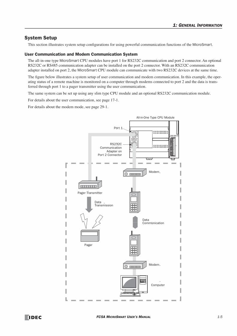
System SetupThis section illustrates system setup configurations for using powerful communication functions of the MicroSmart.
User Communication and Modem Communication SystemThe all-in-one type MicroSmart CPU modules have port 1 for RS232C communication and port 2 connector. An optional RS232C or RS485 communication adapter can be installed on the port 2 connector. With an RS232C communication adapter installed on port 2, the MicroSmart CPU module can communicate with two RS232C devices at the same time.
The figure below illustrates a system setup of user communication and modem communication. In this example, the oper-ating status of a remote machine is monitored on a computer through modems connected to port 2 and the data is trans-ferred through port 1 to a pager transmitter using the user communication.
The same system can be set up using any slim type CPU module and an optional RS232C communication module.
For details about the user communication, see page 17-1.
For details about the modem mode, see page 29-1.
All-in-One Type CPU Module
Pager Transmitter
Pager
Modem
Data Communication
Modem
Computer
Data Transmission
RS232C Communication
Adapter on Port 2 Connector
Port 1
FC5A MICROSMART USER’S MANUAL 1-5
1: GENERAL INFORMATION
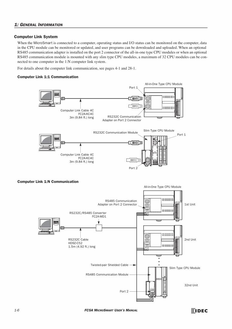
Computer Link SystemWhen the MicroSmart is connected to a computer, operating status and I/O status can be monitored on the computer, data in the CPU module can be monitored or updated, and user programs can be downloaded and uploaded. When an optional RS485 communication adapter is installed on the port 2 connector of the all-in-one type CPU modules or when an optional RS485 communication module is mounted with any slim type CPU modules, a maximum of 32 CPU modules can be con-nected to one computer in the 1:N computer link system.
For details about the computer link communication, see pages 4-1 and 28-1.
Computer Link 1:1 Communication
Computer Link 1:N Communication
Slim Type CPU Module
Computer Link Cable 4C FC2A-KC4C
3m (9.84 ft.) long
All-in-One Type CPU ModulePort 1
RS232C Communication Adapter on Port 2 Connector
Port 2
Computer Link Cable 4C FC2A-KC4C
3m (9.84 ft.) long
Port 1RS232C Communication Module
RS485 Communication Adapter on Port 2 Connector
All-in-One Type CPU Module
RS232C Cable HD9Z-C52 1.5m (4.92 ft.) long
RS232C/RS485 Converter FC2A-MD1
Twisted-pair Shielded Cable
1st Unit
2nd Unit
32nd Unit
Slim Type CPU Module
Port 2
RS485 Communication Module
1-6 FC5A MICROSMART USER’S MANUAL

1: GENERAL INFORMATION
Data Link SystemWith an optional RS485 communication adapter installed on the port 2 connector, one CPU module at the master station can communicate with 31 slave stations through the RS485 line to exchange data and perform distributed control effec-tively. The RS485 terminals are connected with each other using a 2-core twisted pair cable.
The same data link system can also be set up using any slim type CPU modules mounted with RS485 communication modules.
For details about the data link communication, see page 27-1.
Modbus Communication SystemWith an optional RS485 communication adapter installed on the port 2 connector, any FC5A MicroSmart CPU module can be used as a Modbus master or slave station. Using the Modbus communication, the MicroSmart CPU module can exchange data with other Modbus devices.
For details about the Modbus communication, see page 30-1.
Master Station Slave Station 1 Slave Station 31
Master Station Slave Station 1 Slave Station 31
FC5A MICROSMART USER’S MANUAL 1-7
1: GENERAL INFORMATION
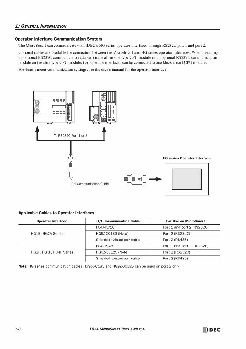
Operator Interface Communication SystemThe MicroSmart can communicate with IDEC’s HG series operator interfaces through RS232C port 1 and port 2.
Optional cables are available for connection between the MicroSmart and HG series operator interfaces. When installing an optional RS232C communication adapter on the all-in-one type CPU module or an optional RS232C communication module on the slim type CPU module, two operator interfaces can be connected to one MicroSmart CPU module.
For details about communication settings, see the user’s manual for the operator interface.
Applicable Cables to Operator Interfaces
Note: HG series communication cables HG9Z-XC183 and HG9Z-3C125 can be used on port 2 only.
Operator Interface O/I Communication Cable For Use on MicroSmart
HG1B, HG2A Series
FC4A-KC1C Port 1 and port 2 (RS232C)
HG9Z-XC183 (Note) Port 2 (RS232C)
Shielded twisted-pair cable Port 2 (RS485)
HG2F, HG3F, HG4F Series
FC4A-KC2C Port 1 and port 2 (RS232C)
HG9Z-3C125 (Note) Port 2 (RS232C)
Shielded twisted-pair cable Port 2 (RS485)
HG series Operator Interface
To RS232C Port 1 or 2
O/I Communication Cable
1-8 FC5A MICROSMART USER’S MANUAL

1: GENERAL INFORMATION
AS-Interface Network
The MicroSmart can be connected to the AS-Interface network using the AS-Interface master module (FC4A-AS62M).
AS-Interface is a type of field bus that is primarily intended to be used to control sensors and actuators. AS-Interface is a network system that is compatible with the IEC62026 standard and is not proprietary to any one manufacturer. A master device can communicate with slave devices such as sensors, actuators, and remote I/Os, using digital and analog signals transmitted over the AS-Interface bus.
The AS-Interface system is comprised of the following three major components:
• One master, such as the MicroSmart AS-Interface master module
• One or more slave devices, such as sensors, actuators, switches, and indicators
• Dedicated 30V DC AS-Interface power supply (26.5 to 31.6V DC)
These components are connected using a two-core cable for both data transmission and AS-Interface power supply. AS-Interface employs a simple yet efficient wiring system and features automatic slave address assignment function, while installation and maintenance are also very easy.
For details about AS-Interface communication, see a separate user’s manual for the MicroSmart AS-Interface master mod-ule (manual No. FC9Y-B644).
Actuator-Sensor-Interface, abbreviated AS-Interface
Light Curtain
Open Network (DeviceNet, CC-Link)
AS-Interface Gateway
AS-Interface Safety Monitor
AS-Interface Safety at Work
Emergency Stop Switch
Manifold Solenoid Valve
Light Tower(AS-Interface Direct Connection Type)
MicroSmart AS-Interface Master Module
PS2R AS-Interface Power Supply
SX5A AS-Interface Communication TerminalIP67 Outside-panel Type
SX5A AS-Interface Communication TerminalIP20 Inside-panel Type
SwitchNet Control Units(AS-Interface Direct Connection Type)
Sensor(AS-Interface Direct Connection Type)
Sensor
The AS-Interface Safety Monitor is required to connect safety devices, such as the light curtain and emergency stop switch, to the AS-Interface line.
SwitchNet is an IDEC trademark for pushbuttons, pilot lights, and other control units capable of direct connection to the AS-Interface. SwitchNet devices are completely compatible with AS-Interface Ver. 2.1.
TM
Maximum Communication DistanceWithout repeater: 100 m With 2 repeaters: 300 m
FC5A MICROSMART USER’S MANUAL 1-9

1: GENERAL INFORMATION
Web Server Unit FC4A-SX5ES1EA New Powerful Tool for the MicroSmart to communicate through Ethernet
• Email messages can be sent to PCs and mobile phones to alert a user by programming the MicroSmart to receive inputs of abnormal machine conditions.
• Ethernet communication between the MicroSmart and PC enables remote maintenance.
• User communication enables 1:1 communication between MicroSmart CPU modules via Ethernet.
• Allows for access to data within the MicroSmart using a standard web browser.
• Connect to the MicroSmart and as well as any operator interface with an ethernet interface and a TCP/IP client function.
For details about the web server unit, see the separate brochure and user’s manual.
Sending Email messages
Remote monitoring and control
Data exchange between two MicroSmart CPU modules
• The MicroSmart is programmed to detect abnormal conditions of machines. When an error occurs, an email message is sent to the address of PCs and mobile phones registered within the web server unit.
Web Server Unit
PLC1
PLC2 Email Server
Internet
PC
Mobile Phone
Ethernet
• Operating conditions of machines can be easily monitored and changed from remote places.
• WindLDR functions can be used on a MicroSmart installed in remote places, for monitoring of machines, configuration, and to upload user programs. The Micro-Smart does not need special user pro-grams to communicate with a PC. Also, not only WindLDR but standard SCADA software applicable to Ethernet enables graphical displays of monitoring and main-tenance status.
PLC1
Ethernet
PLC2 PLC3
PC1 PC2
• Data can be exchanged between Micro-Smart cpu modules connected with web server units using the user communica-tion function.
PLC3
Ethernet
PLC4
PLC1 PLC2
1-10 FC5A MICROSMART USER’S MANUAL

1: GENERAL INFORMATION
Basic SystemThe all-in-one 10-I/O type CPU module has 6 input terminals and 4 output terminals. The 16-I/O type CPU module has 9 input terminals and 7 output terminals. The 24-I/O type CPU module has 14 input terminals and 10 output terminals. Only the 24-I/O type CPU module has an expansion connector to connect I/O modules. When four 16-point input or output modules are connected to the 24-I/O type CPU module, the I/O points can be expanded to a maximum of 88 points.
Any slim type CPU module can add a maximum of seven expansion I/O modules. When using an expansion interface module, eight more expansion I/O modules can be added. For details, see page 2-58.
4 I/O modules maximumAll-in-One 24-I/O Type CPU Module
FC5A MICROSMART USER’S MANUAL 1-11

1: GENERAL INFORMATION
1-12 FC5A MICROSMART USER’S MANUAL

2: MODULE SPECIFICATIONS
IntroductionThis chapter describes MicroSmart modules, parts names, and specifications of each module.
Available modules include all-in-one type and slim type CPU modules, digital input modules, digital output modules, mixed I/O modules, analog I/O modules, HMI module, HMI base module, communication adapters, communication mod-ules, memory cartridge, and clock cartridge.
CPU Modules (All-in-One Type)All-in-one type CPU modules are available in 10-, 16-, and 24-I/O types. The 10-I/O type has 6 input and 4 output termi-nals, the 16-I/O type 9 input and 7 output terminals, and the 24-I/O type 14 input and 10 output terminals. Every all-in-one type CPU module has communication port 1 for RS232C communication and port 2 connector to install an optional RS232C or RS485 communication adapter for 1:N computer link, modem communication, or data link communication. Every all-in-one type CPU module has a cartridge connector to install an optional memory cartridge or clock cartridge.
CPU Module Type Numbers (All-in-One Type)
Parts Description (All-in-One Type)
Power Voltage 10-I/O Type 16-I/O Type 24-I/O Type
100 -240V AC (50/60 Hz) FC5A-C10R2 FC5A-C16R2 FC5A-C24R2
24V DC FC5A-C10R2C FC5A-C16R2C FC5A-C24R2C
(3) Input Terminals
(5) Expansion Connector
(6) Input LED (IN)
From Left:(7) Power LED (PWR)(8) Run LED (RUN)(9) Error LED (ERR)(10) Status LED (STAT)(11) Output LED (OUT)
(2) Sensor Power Terminals
(12) Port 1
(13) Analog Potentiometer
(14) Port 2 Connector
Bottom View
(15) Cartridge Connector
(1) Power Supply Terminals
(4) Output Terminals
(17) Hinged Lid
(16) Terminal Cover(20) Expansion
Connector Seal
(16) Terminal CoverThese figures illustrate the 24-I/O type CPU module.Functions of each part are described on the following page. (19) Dummy Cartridge
(18) HMI Connector Cover
FC5A MICROSMART USER’S MANUAL 2-1

2: MODULE SPECIFICATIONS
(1) Power Supply TerminalsConnect power supply to these terminals. Power voltage 100-240V AC or 24V DC. See page 3-17.
(2) Sensor Power Terminals (AC power type only)For supplying power to sensors (24V DC, 250mA). These terminals can be used for supplying power to input cir-cuits. Use the sensor power supply only for supplying power to input devices connected to the MicroSmart.
(3) Input TerminalsFor connecting input signals from input devices such as sensors, pushbuttons, and limit switches. The input termi-nals accept both sink and source DC input signals.
(4) Output TerminalsFor connecting output signals to output devices such as electromechanical relays and solenoid valves. The inter-nal output relay is rated at 240V AC/2A or 30V DC/2A.
(5) Expansion Connector (24-I/O type CPU module only)For connecting digital and analog I/O modules to the 24-I/O type CPU module.
(6) Input LED (IN)Turns on when a corresponding input is on.
(7) Power LED (PWR)Turns on when power is supplied to the CPU module.
(8) Run LED (RUN)Turns on when the CPU module is executing the user program.
(9) Error LED (ERR)Turns on when an error has occurred in the CPU module.
(10) Status LED (STAT)The status LED can be turned on or off using the user program to indicate a specified status.
(11) Output LED (OUT)Turns on when a corresponding output is on.
(12) Port 1 (RS232C)For connecting a computer to download a user program and monitor the PLC operation on a computer using WindLDR.
(13) Analog PotentiometerSets a value of 0 through 255 to a special data register. The 10- and 16-I/O types have one potentiometer. The 24-I/O type has two potentiometers. The analog potentiometer can be used to set a preset value for an analog timer.
(14) Port 2 ConnectorFor connecting an optional RS232C or RS485 communication adapter.
(15) Cartridge ConnectorFor connecting an optional memory cartridge or clock cartridge.
(16) Terminal CoverFor protecting the input and output terminals. When wiring the terminals, open the covers.
(17) Hinged LidOpen the lid to gain access to the port 1, port 2 connector, and analog potentiometer.
(18) HMI Connector CoverRemove the HMI connector cover when using an optional HMI module.
(19) Dummy CartridgeRemove the dummy cartridge when using an optional memory cartridge or clock cartridge.
(20) Expansion Connector Seal (24-I/O type CPU module only)Remove the expansion connector seal when connecting an expansion module.
10-I/O Type0 1 2 3 4 5
IN
P R E S 0 1 2 3WR
UN
RR
TAT
OUT
16-I/O Type0 1 2 3 4 5 6 7 10
IN
P R E S 0 1 2 3 4 5 6WR
UN
RR
TAT
OUT
24-I/O Type0 1 2 3 4 5 6 7 10 11 12 13 14 15
IN
P R E S 0 1 2 3 4 5 6 7 10 11WR
UN
RR
TAT
OUT
LED Indicators
2-2 FC5A MICROSMART USER’S MANUAL

2: MODULE SPECIFICATIONS
General Specifications (All-in-One Type CPU Module)
Normal Operating Conditions
Power Supply (AC Power Type)
Note 1: Power consumption by the CPU module, including 250mA sensor power
Note 2: Power consumption by the CPU module, including 250mA sensor power, and four I/O modules
Note: The maximum number of relay outputs that can be turned on simultaneously is 33 points (AC power type CPU module) including relay outputs on the CPU module.
CPU ModuleAC Power Type FC5A-C10R2 FC5A-C16R2 FC5A-C24R2
DC Power Type FC5A-C10R2C FC5A-C16R2C FC5A-C24R2C
Operating Temperature 0 to 55°C (operating ambient temperature)
Storage Temperature –25 to +70°C (no freezing)
Relative Humidity 10 to 95% (non-condensing, operating and storage humidity)
Pollution Degree 2 (IEC 60664-1)
Degree of Protection IP20 (IEC 60529)
Corrosion Immunity Atmosphere free from corrosive gases
AltitudeOperation: 0 to 2,000m (0 to 6,565 feet)Transport: 0 to 3,000m (0 to 9,840 feet)
Vibration ResistanceWhen mounted on a DIN rail or panel surface:5 to 9 Hz amplitude 3.5 mm, 9 to 150 Hz acceleration 9.8 m/s2 (1G)2 hours per axis on each of three mutually perpendicular axes (IEC 61131-2)
Shock Resistance147 m/s2 (15G), 11 ms duration, 3 shocks per axis on three mutually perpendicular axes (IEC 61131-2)
ESD Immunity Contact discharge: ±4 kV, Air discharge: ±8 kV (IEC 61000-4-2)
WeightAC Power Type 230g 250g 305g
DC Power Type 240g 260g 310g
CPU Module FC5A-C10R2 FC5A-C16R2 FC5A-C24R2
Rated Power Voltage 100 to 240V AC
Allowable Voltage Range 85 to 264V AC
Rated Power Frequency 50/60 Hz (47 to 63 Hz)
Maximum Input Current 250 mA (85V AC) 300 mA (85V AC) 450 mA (85V AC)
Maximum Power Consumption30VA (264V AC), 20VA (100V AC) (Note 1)
31VA (264V AC), 22VA (100V AC) (Note 1)
40VA (264V AC), 33VA (100V AC) (Note 2)
Allowable Momentary Power Interruption
10 ms (at the rated power voltage)
Dielectric StrengthBetween power and terminals: 1,500V AC, 1 minute Between I/O and terminals: 1,500V AC, 1 minute
Insulation ResistanceBetween power and terminals: 10 MΩ minimum (500V DC megger) Between I/O and terminals: 10 MΩ minimum (500V DC megger)
Noise ResistanceAC power terminals: 1.5 kV, 50 ns to 1 µs I/O terminals (coupling clamp): 1.5 kV, 50 ns to 1 µs
Inrush Current 35A maximum 35A maximum 40A maximum
Grounding Wire UL1007 AWG16
Power Supply Wire UL1015 AWG22, UL1007 AWG18
Effect of Improper Power Supply Connection
Reverse polarity: Normal operation (AC) Improper voltage or frequency: Permanent damage may be caused Improper lead connection: Permanent damage may be caused
FC5A MICROSMART USER’S MANUAL 2-3

2: MODULE SPECIFICATIONS
Power Supply (DC Power Type)
Note 1: Power consumption by the CPU module
Note 2: Power consumption by the CPU module and four I/O modules
Note: The maximum number of relay outputs that can be turned on simultaneously is 44 points (DC power type CPU module) including relay outputs on the CPU module.
Function Specifications (All-in-One Type CPU Module)
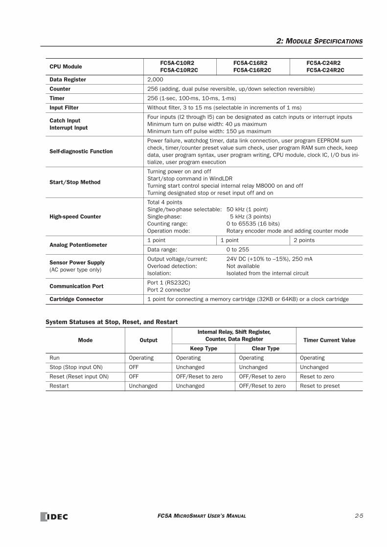
CPU Module Specifications
CPU Module FC5A-C10R2C FC5A-C16R2C FC5A-C24R2C
Allowable Voltage Range DC power type: 20.4 to 28.8V DC
Maximum Input Current 160 mA (24V DC) 190 mA (24V DC) 360 mA (24V DC)
Maximum Power Consumption3.9W (24V DC) (Note 1)
4.6W (24V DC) (Note 1)
8.7W (24V DC) (Note 2)
Allowable Momentary Power Interruption
10 ms (at the rated power voltage)
Dielectric StrengthBetween power and terminals: 1,500V AC, 1 minute Between I/O and terminals: 1,500V AC, 1 minute
Insulation ResistanceBetween power and terminals: 10 MΩ minimum (500V DC megger) Between I/O and terminals: 10 MΩ minimum (500V DC megger)
Noise ResistanceDC power terminals: 1.0 kV, 50 ns to 1 µs I/O terminals (coupling clamp): 1.5 kV, 50 ns to 1 µs
Inrush Current 35A maximum 35A maximum 40A maximum
Grounding Wire UL1007 AWG16
Power Supply Wire UL1015 AWG22, UL1007 AWG18
Effect of Improper Power Supply Connection
Reverse polarity: No operation, no damage Improper voltage or frequency: Permanent damage may be caused Improper lead connection: Permanent damage may be caused
CPU ModuleFC5A-C10R2FC5A-C10R2C
FC5A-C16R2FC5A-C16R2C
FC5A-C24R2FC5A-C24R2C
Program Capacity13,800 bytes(2,300 steps)
27,000 bytes(4,500 steps)
54,000 bytes(9,000 steps)
Expandable I/O Modules — — 4 modules
I/O PointsInput 6 9 14 Expansion:
64Output 4 7 10
User Program Storage EEPROM (10,000 rewriting life)
RAM Backup
Backup Duration Approx. 30 days (typical) at 25°C after backup battery fully charged
Backup Data Internal relay, shift register, counter, data register
Battery Lithium secondary battery
Charging Time Approx. 15 hours for charging from 0% to 90% of full charge
Battery Life 5 years in cycles of 9-hour charging and 15-hour discharging
Replaceability Impossible to replace battery
Control System Stored program system
Instruction Words35 basic76 advanced
35 basic76 advanced
35 basic81 advanced
Processing Time
Basic instruction 1.16 ms (1000 steps) See page A-1.
END processing0.64 ms (not including expansion I/O service, clock function processing, data link processing, and interrupt processing) See page A-4.
Internal Relay 2048
Shift Register 128
2-4 FC5A MICROSMART USER’S MANUAL
2: MODULE SPECIFICATIONS
System Statuses at Stop, Reset, and Restart
Data Register 2,000
Counter 256 (adding, dual pulse reversible, up/down selection reversible)
Timer 256 (1-sec, 100-ms, 10-ms, 1-ms)
Input Filter Without filter, 3 to 15 ms (selectable in increments of 1 ms)
Catch InputInterrupt Input
Four inputs (I2 through I5) can be designated as catch inputs or interrupt inputsMinimum turn on pulse width: 40 µs maximumMinimum turn off pulse width: 150 µs maximum
Self-diagnostic Function
Power failure, watchdog timer, data link connection, user program EEPROM sum check, timer/counter preset value sum check, user program RAM sum check, keep data, user program syntax, user program writing, CPU module, clock IC, I/O bus ini-tialize, user program execution
Start/Stop Method
Turning power on and offStart/stop command in WindLDRTurning start control special internal relay M8000 on and offTurning designated stop or reset input off and on
High-speed Counter
Total 4 pointsSingle/two-phase selectable: 50 kHz (1 point)Single-phase: 5 kHz (3 points)Counting range: 0 to 65535 (16 bits)Operation mode: Rotary encoder mode and adding counter mode
Analog Potentiometer1 point 1 point 2 points
Data range: 0 to 255
Sensor Power Supply(AC power type only)
Output voltage/current: 24V DC (+10% to –15%), 250 mAOverload detection: Not availableIsolation: Isolated from the internal circuit
Communication PortPort 1 (RS232C) Port 2 connector
Cartridge Connector 1 point for connecting a memory cartridge (32KB or 64KB) or a clock cartridge
Mode OutputInternal Relay, Shift Register,
Counter, Data Register Timer Current ValueKeep Type Clear Type
Run Operating Operating Operating Operating
Stop (Stop input ON) OFF Unchanged Unchanged Unchanged
Reset (Reset input ON) OFF OFF/Reset to zero OFF/Reset to zero Reset to zero
Restart Unchanged Unchanged OFF/Reset to zero Reset to preset
CPU ModuleFC5A-C10R2FC5A-C10R2C
FC5A-C16R2FC5A-C16R2C
FC5A-C24R2FC5A-C24R2C
FC5A MICROSMART USER’S MANUAL 2-5

2: MODULE SPECIFICATIONS
Communication Function
Note 1: 1:1 Modbus communication only
Note 2: For special cables, see page A-7.
Note 3: Recommended cable for RS485: Twisted-pair shielded cable with a minimum core wire of 0.3 mm2. Conductor resistance 85 Ω/km maximum, shield resistance 20 Ω/km maximum.
Memory Cartridge (Option)
Clock Cartridge (Option)
Communication Port Port 1 Port 2
Communication Adapter — FC4A-PC1 FC4A-PC2 FC4A-PC3
Communication Module — FC4A-HPC1 FC4A-HPC2 FC4A-HPC3
Standards EIA RS232C EIA RS232C EIA RS485 EIA RS485
Maximum Baud Rate 57,600 bps 57,600 bps 57,600 bps 57,600 bps
Maintenance Communication (Computer Link)
Possible Possible Possible Possible
User Communication Possible Possible — Possible
Modem Communication — Possible — —
Data Link Communication — — —Possible (31 slaves max.)
Modbus Communication — Possible (Note 1) — Possible
Maximum Cable LengthSpecial cable (Note 2)
Special cable (Note 2)
Special cable (Note 2)
200m (Note 3)
Isolation between Internal Circuit and Communication Port
Not isolated Not isolated Not isolated Not isolated
Memory Type EEPROM
Accessible Memory Capacity
32 KB, 64 KBThe maximum program capacity depends on the CPU module.When using the 32 KB memory cartridge on the 24-I/O type CPU module, the maxi-mum program capacity is limited to 30,000 bytes.
Hardware for Storing Data CPU module
Software for Storing Data WindLDR
Quantity of Stored Programs One user program can be stored on one memory cartridge.
Program Execution PriorityWhen a memory cartridge is installed, the user program on the memory cartridge is executed. User programs can be downloaded from the memory cartridge to the CPU module.
Accuracy ±30 sec/month (typical) at 25°C
Backup Duration Approx. 30 days (typical) at 25°C after backup battery fully charged
Battery Lithium secondary battery
Charging Time Approx. 10 hours for charging from 0% to 90% of full charge
Battery Life Approx. 100 recharge cycles after discharging down to 10% of full charge
Replaceability Impossible to replace battery
2-6 FC5A MICROSMART USER’S MANUAL

2: MODULE SPECIFICATIONS
DC Input Specifications (All-in-One Type CPU Module)
Input Operating Range Input Internal CircuitThe input operating range of Type 1 and Type 2 (IEC 61131-2) input modules is shown below:
CPU ModuleFC5A-C10R2FC5A-C10R2C
FC5A-C16R2FC5A-C16R2C
FC5A-C24R2FC5A-C24R2C
Input Points and Common Line6 points in 1 common line
9 points in 1 common line
14 points in 1 common line
Terminal Arrangement See CPU Module Terminal Arrangement on pages 2-9 and 2-10.
Rated Input Voltage 24V DC sink/source input signal
Input Voltage Range 20.4 to 28.8V DC
Rated Input CurrentI0 and I1: 6.4 mA (24V DC)I2 to I7, I10 to I15: 7 mA/point (24V DC)
Input ImpedanceI0 and I1: 3.7 kΩI2 to I7, I10 to I15: 3.4 kΩ
Turn ON TimeI0 and I1: 2 µs + filter valueI2 to I5: 35 µs + filter valueI6, I7, I10 to I15: 40 µs + filter value
Turn OFF TimeI0 and I1: 16 µs + filter valueI2 to I5: 150 µs + filter valueI2 to I7, I10 to I15: 150 µs + filter value
IsolationBetween input terminals: Not isolated Internal circuit: Photocoupler isolated
Input Type Type 1, Type 2 (IEC 61131)
External Load for I/O Interconnection Not needed
Signal Determination Method Static
Effect of Improper Input ConnectionBoth sinking and sourcing input signals can be connected. If any input exceeding the rated value is applied, permanent damage may be caused.
Cable Length 3m (9.84 ft.) in compliance with electromagnetic immunity
Input
Inte
rnal
Circ
uit
COM
3.3 kΩInput
Inte
rnal
Circ
uit
COM
3.3 kΩ
Inputs I0 and I1 Inputs I2 to I15
Inpu
t Vo
ltage
(V
DC
)
28.8
0100
I/O Simultaneous ON Ratio (%)
26.4
When using at 45°C, all I/Os can be turned on simultaneously at input volt-age 28.8V DC as indicated with line (2).
When using the FC5A-C10R2/C, all I/Os can be turned on simultaneously at 55°C, input voltage 28.8V DC.
For other possible mounting direc-tions, see page 3-13.
(2) 45°C
(1) 55°C
700
I/O Usage LimitsWhen using the FC5A-C16R2/C or FC5A-C24R2/C at an ambient temperature of 55°C in the normal mounting direction, limit the inputs and outputs, respectively, which turn on simultaneously along line (1).
Inputs I2 to I15
Transition
OFF AreaInpu
t Vo
ltage
(V
DC
)
28.8
15
5
00.9 7.9
Input Current (mA)
ON Area
Area
6.43.7
24
Inputs I0 and I1
Transition
OFF AreaInpu
t Vo
ltage
(V
DC
)
28.8
15
5
01.2 8.4
Input Current (mA)
ON Area
Area
74.2
24
FC5A MICROSMART USER’S MANUAL 2-7

2: MODULE SPECIFICATIONS
Relay Output Specifications (All-in-One Type CPU Module)
Output Delay
CPU ModuleFC5A-C10R2FC5A-C10R2C
FC5A-C16R2FC5A-C16R2C
FC5A-C24R2FC5A-C24R2C
No. of Outputs 4 points 7 points 10 points
Output Points per Common Line
COM0 3 NO contacts 4 NO contacts 4 NO contacts
COM1 1 NO contact 2 NO contacts 4 NO contacts
COM2 — 1 NO contact 1 NO contact
COM3 — — 1 NO contact
Terminal Arrangement See CPU Module Terminal Arrangement on pages 2-9 and 2-10.
Maximum Load Current(resistive/inductive load)
2A per point8A per common line
Minimum Switching Load 0.1 mA/0.1V DC (reference value)
Initial Contact Resistance 30 mΩ maximum
Electrical Life 100,000 operations minimum (rated load 1,800 operations/hour)
Mechanical Life 20,000,000 operations minimum (no load 18,000 operations/hour)
Rated Load240V AC/2A (resistive load, inductive load cos ø = 0.4) 30V DC/2A (resistive load, inductive load L/R = 7 ms)
Dielectric StrengthBetween output and or terminals: 1,500V AC, 1 minute Between output terminal and internal circuit: 1,500V AC, 1 minute Between output terminals (COMs): 1,500V AC, 1 minute
Contact Protection Circuit for Relay Output See page 3-16.
Command
Output Relay Status
OFF delay: 10 ms maximum
Chatter: 6 ms maximum
ON delay: 6 ms maximum
ON
OFF
ON
OFF
2-8 FC5A MICROSMART USER’S MANUAL

2: MODULE SPECIFICATIONS
CPU Module Terminal Arrangement (All-in-One Type)The input and output terminal arrangements of the all-in-one type CPU modules are shown below.
AC Power Type CPU Module
FC5A-C10R2
FC5A-C16R2
FC5A-C24R2
L N100-240VAC Ry.OUT Ry.OUT
COM0 COM1 30 1 2
+24V 0VDC OUT COM
DC IN 0 1 2 3 4 5
Sensor Power Terminals Input Terminals
AC Power Terminals Output Terminals
+24V 0V 10DC OUT COM
DC IN 0 1 2 3 4 5 6 7
L N100-240VAC Ry.OUT
COM0Ry.OUTCOM1 4 5
Ry.OUTCOM2 60 1 2 3
Sensor Power Terminals Input Terminals
AC Power Terminals Output Terminals
+24V 0V 10 11 12 13 14 15DC OUT COM
DC IN 0 1 2 3 4 5 6 7
L N100-240VAC Ry.OUT
COM0Ry.OUTCOM1
Ry.OUTCOM3 11
Ry.OUTCOM2 100 1 2 3 4 5 6 7
Sensor Power Terminals Input Terminals
AC Power Terminals Output Terminals
FC5A MICROSMART USER’S MANUAL 2-9

2: MODULE SPECIFICATIONS
DC Power Type CPU Module
FC5A-C10R2C
FC5A-C16R2C
FC5A-C24R2C
Ry.OUT Ry.OUTCOM0 COM1 30 1 2
COMDC IN 0 1 2 3 4 5
+ –24VDC
Input Terminals
DC Power Terminals Output Terminals
10COMDC IN 0 1 2 3 4 5 6 7
Ry.OUTCOM0
Ry.OUTCOM1 4 5
Ry.OUTCOM2 60 1 2 3+ –
24VDC
Input Terminals
DC Power Terminals Output Terminals
10 11 12 13 14 15COMDC IN 0 1 2 3 4 5 6 7
Ry.OUTCOM0
Ry.OUTCOM1
Ry.OUTCOM3 11
Ry.OUTCOM2 100 1 2 3 4 5 6 7+ –
24VDC
Input Terminals
DC Power Terminals Output Terminals
2-10 FC5A MICROSMART USER’S MANUAL
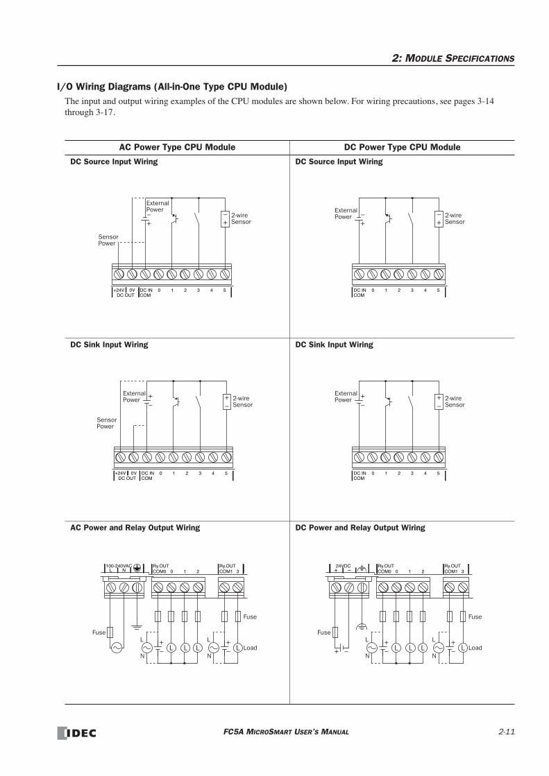
2: MODULE SPECIFICATIONS
I/O Wiring Diagrams (All-in-One Type CPU Module)The input and output wiring examples of the CPU modules are shown below. For wiring precautions, see pages 3-14 through 3-17.
AC Power Type CPU Module DC Power Type CPU Module
DC Source Input Wiring DC Source Input Wiring
DC Sink Input Wiring DC Sink Input Wiring
AC Power and Relay Output Wiring DC Power and Relay Output Wiring
+24V 0VDC OUT COM
DC IN 0 1 2 3 4 5
+–
+–
Sensor
External Power
2-wireSensor
Power
+–
+–External
Power 2-wire
COMDC IN 0 1 2 3 4 5
Sensor
+24V 0VDC OUT COM
DC IN 0 1 2 3 4 5
+–
+–
Sensor
External Power 2-wire
Sensor
Power
COMDC IN 0 1 2 3 4 5
+–
+–
External Power 2-wire
Sensor
L N100-240VAC Ry.OUT Ry.OUT
COM0 COM1 30 1 2
+– LLL L
+–
L
N
L
N
Fuse
Fuse
Load
Ry.OUT Ry.OUTCOM0 COM1 30 1 2+ –
24VDC
+– LLL L
+–
L
N
L
N
Fuse
Fuse
Load+ –
FC5A MICROSMART USER’S MANUAL 2-11

2: MODULE SPECIFICATIONS
CPU Modules (Slim Type)Slim type CPU modules are available in 16- and 32-I/O types. The 16-I/O type has 8 input and 8 output terminals, and the 32-I/O type has 16 input and 16 output terminals. The FC5A-D16RK1 and FC5A-D16RS1 have 2 transistor outputs used for high-speed outputs and pulse outputs in addition to 6 relay outputs. Every slim type CPU module has communication port 1 for RS232C communication, and can mount an optional RS232C or RS485 communication module for 1:N com-puter link, modem communication, and data link communication. The HMI base module can also be mounted to install an optional HMI module and a communication adapter. Every slim type CPU module has two cartridge connectors to install an optional memory cartridge and a clock cartridge.
CPU Module Type Numbers (Slim Type)
Parts Description (Slim Type)
I/O Points Output Type High-speed Transistor Output (Q0 & Q1) Type No.
16 (8 in / 8 out)Relay Output 240V AC/30V DC, 2A
Sink Output 0.3A FC5A-D16RK1
Source Output 0.3A FC5A-D16RS1
32 (16 in / 16 out)Transistor Sink Output 0.3A FC5A-D32K3
Transistor Source Output 0.3A FC5A-D32S3
(3) Expansion Connector
(4) Power LED (PWR)(5) Run LED (RUN)(6) Error LED (ERR)(7) Status LED (STAT)(8) Input LED (DC.IN)(9) Output LED (Tr.OUT or Ry.OUT)(12) Port 1
(10) Analog Potentiometer
Side View
(14) Cartridge Connector 2
(1) Power Supply Terminals (2) I/O Terminals
(16) Hinged Lid(18) Expansion
Connector Seal
These figures illustrate the 32-I/O type CPU module.Functions of each part are described on the following page.
(17) Dummy Cartridges
(15) Communication Connector
(11) Analog Voltage Input Connector
(13) Cartridge Connector 1
2-12 FC5A MICROSMART USER’S MANUAL

2: MODULE SPECIFICATIONS
(1) Power Supply TerminalsConnect power supply to these terminals. Power voltage 24V DC. See page 3-18.
(2) I/O TerminalsFor connecting input and output signals. The input terminals accept both sink and source 24V DC input signals. Transistor and relay output types are available. Transistor output type has MIL connectors and relay output type has removable screw connectors.
(3) Expansion ConnectorFor connecting digital and analog I/O modules.
(4) Power LED (PWR)Turns on when power is supplied to the CPU module.
(5) Run LED (RUN)Turns on when the CPU module is executing the user program.
(6) Error LED (ERR)Turns on when an error occurs in the CPU module.
(7) Status LED (STAT)The status LED can be turned on or off using the user program to indicate a specified status.
(8) Input LED (IN)Turns on when a corresponding input is on.
(9) Output LED (Tr.OUT or Ry.OUT)Turns on when a corresponding output is on.
(10) Analog PotentiometerSets a value of 0 through 255 to a special data register. All slim type CPU modules have one potentiometer, which can be used to set a preset value for an analog timer.
(11) Analog Voltage Input ConnectorFor connecting an analog voltage source of 0 through 10V DC. The analog voltage is converted to a value of 0 through 255 and stored to a special data register.
(12) Port 1 (RS232C)For connecting a computer to download a user program and monitor the PLC operation on a computer using WindLDR.
(13) Cartridge Connector 1For connecting an optional memory cartridge or clock cartridge.
(14) Cartridge Connector 2For connecting an optional memory cartridge or clock cartridge.
(15) Communication ConnectorFor connecting an optional communication module or HMI base module. Remove the connector cover before con-necting a module.
(16) Hinged LidOpen the lid to gain access to the port 1, cartridge connectors 1 and 2, analog potentiometer, and analog voltage input connector.
(17) Dummy CartridgesRemove the dummy cartridge when using an optional memory cartridge or clock cartridge.
(18) Expansion Connector SealRemove the expansion connector seal when connecting an expansion module.
LED Indicators
32-I/O Type (Transistor Output)
1011121314151617
1011121314151617
16-I/O Type (Relay Output)
PWRRUNERRSTAT
DC.IN
67
01
Ry.OUT
2345
Tr.OUT
PWRRUNERRSTAT
01234567
01234567
DC.IN Tr.OUT Tr.OUT
DC.IN
67
012345
FC5A MICROSMART USER’S MANUAL 2-13

2: MODULE SPECIFICATIONS
General Specifications (Slim Type CPU Module)
Normal Operating Conditions
Power Supply
Note: Among relay outputs on the CPU module and relay output modules connected to the CPU module, a maximum of 54 points can be turned on simultaneously. Among relay outputs connected beyond the expansion module, a maximum of 54 points can be turned on simultaneously. Relay outputs exceeding these limits may not turn on correctly.
CPU ModuleFC5A-D16RK1FC5A-D16RS1
FC5A-D32K3FC5A-D32S3
Operating Temperature 0 to 55°C (operating ambient temperature)
Storage Temperature –25 to +70°C
Relative Humidity 10 to 95% (non-condensing, operating and storage humidity)
Pollution Degree 2 (IEC 60664-1)
Degree of Protection IP20 (IEC 60529)
Corrosion Immunity Atmosphere free from corrosive gases
AltitudeOperation: 0 to 2,000m (0 to 6,565 feet)Transport: 0 to 3,000m (0 to 9,840 feet)
Vibration ResistanceWhen mounted on a DIN rail or panel surface:5 to 9 Hz amplitude 3.5 mm, 9 to 150 Hz acceleration 9.8 m/s2 (1G)2 hours per axis on each of three mutually perpendicular axes (IEC 61131-2)
Shock Resistance147 m/s2 (15G), 11 ms duration, 3 shocks per axis on three mutually perpendicular axes (IEC 61131-2)
ESD Immunity Contact discharge: ±4 kV, Air discharge: ±8 kV (IEC 61000-4-2)
Weight 230g 190g
Rated Power Voltage 24V DC
Allowable Voltage Range 20.4 to 26.4V DC (including ripple)
Maximum Input Current 700 mA (26.4V DC) 700 mA (26.4V DC)
Maximum Power ConsumptionCPU module + 7 I/O modules + expansion module + 8 I/O modules
19W (26.4V DC) 19W (26.4V DC)
Allowable Momentary Power Interruption
10 ms (at 24V DC)
Dielectric StrengthBetween power and terminals: 500V AC, 1 minute Between I/O and terminals: 1,500V AC, 1 minute
Insulation ResistanceBetween power and terminals: 10 MΩ minimum (500V DC megger) Between I/O and terminals: 10 MΩ minimum (500V DC megger)
Noise ResistanceDC power terminals: 1.0 kV, 50 ns to 1 µs I/O terminals (coupling clamp): 1.5 kV, 50 ns to 1 µs
Inrush Current 50A maximum (24V DC)
Grounding Wire UL1015 AWG22, UL1007 AWG18
Power Supply Wire UL1015 AWG22, UL1007 AWG18
Effect of Improper Power Supply Connection
Reverse polarity: No operation, no damage Improper voltage or frequency: Permanent damage may be caused Improper lead connection: Permanent damage may be caused
2-14 FC5A MICROSMART USER’S MANUAL

2: MODULE SPECIFICATIONS
Function Specifications (Slim Type CPU Module)
CPU Module Specifications
CPU ModuleFC5A-D16RK1FC5A-D16RS1
FC5A-D32K3FC5A-D32S3
Program Capacity 62,400 bytes (10,400 steps)
Expandable I/O Modules 7 modules + additional 8 modules using the expansion interface module
I/O PointsInput 8 Expansion: 224 (Note 1)
Additional: 256 (Note 2)16 Expansion: 224 (Note 1)
Additional: 256 (Note 2)Output 8 16
User Program Storage EEPROM
RAM Backup
Backup Duration Approx. 30 days (typical) at 25°C after backup battery fully charged
Backup Data Internal relay, shift register, counter, data register, expansion data register
Battery Lithium secondary battery
Charging Time Approx. 15 hours for charging from 0% to 90% of full charge
Battery Life 5 years in cycles of 9-hour charging and 15-hour discharging
Replaceability Impossible to replace battery
Control System Stored program system
Instruction Words35 basic 88 advanced
35 basic 92 advanced
Processing Time
Basic instruction 83 µs (1000 steps) See page A-1.
END processing0.35 ms (not including expansion I/O service, clock function processing, data link processing, and interrupt processing) See page A-4.
Internal Relay 2,048
Shift Register 256
Data Register 2,000
Expansion Data Register 6,000
Extra Data Register 40,000 (Note 3)
Counter 256 (adding, dual pulse reversible, up/down selection reversible)
Timer 256 (1-sec, 100-ms, 10-ms, 1-ms)
Input Filter Without filter, 3 to 15 ms (selectable in increments of 1 ms)
Catch InputInterrupt Input
Four inputs (I2 through I5) can be designated as catch inputs or interrupt inputsMinimum turn on pulse width: 5 µs maximumMinimum turn off pulse width: 5 µs maximum
Self-diagnostic Function
Power failure, watchdog timer, data link connection, user program EEPROM sum check, timer/counter preset value sum check, user program RAM sum check, keep data, user program syntax, user program writing, CPU module, clock IC, I/O bus initialize, user program execution
Start/Stop Method
Turning power on and offStart/stop command in WindLDRTurning start control special internal relay M8000 on and offTurning designated stop or reset input off and on
High-speed Counter
Total 4 pointsSingle/two-phase selectable: 100 kHz (2 points)Single-phase: 100 kHz (2 points)Counting range: 0 to 4,294,967,295 (32 bits)Operation mode: Rotary encoder mode and adding counter mode
Analog Potentiometer1 point 1 point
Data range: 0 to 255
FC5A MICROSMART USER’S MANUAL 2-15

2: MODULE SPECIFICATIONS
Note 1: The maximum number of outputs that can be turned on simultaneously is 54 including those on the CPU module.
Note 2: Among the additional I/O modules, the maximum number of outputs that can be turned on simultaneously is 54.
Note 3: Extra data registers D10000 through D49999 are enabled using WindLDR Function Area Settings, then run-time pro-gram download cannot be used.
System Statuses at Stop, Reset, and Restart
Note: All expansion data registers are keep types.
Communication Function
Note 1: 1:1 Modbus communication only
Note 2: For special cables, see page A-7.
Note 3: Recommended cable for RS485: Twisted-pair shielded cable with a minimum core wire of 0.3 mm2. Conductor resistance 85 Ω/km maximum, shield resistance 20 Ω/km maximum.
Analog Voltage Input
Quantity: 1 pointInput voltage range: 0 to 10V DCInput impedance: Approx. 100 kΩData range: 0 to 255 (8 bits)
Pulse Output2 points 3 points
Maximum frequency: 100 kHz
Communication PortPort 1 (RS232C) Communication connector for port 2
Cartridge Connector 2 points for connecting a memory cartridge (32KB or 64KB) and a clock cartridge
Mode OutputInternal Relay, Shift Register, Counter, Data Register, Expansion DR, Extra DR Timer Current Value
Keep Type Clear Type
Run Operating Operating Operating Operating
Stop (Stop input ON) OFF Unchanged Unchanged Unchanged
Reset (Reset input ON) OFF OFF/Reset to zero OFF/Reset to zero Reset to zero
Restart Unchanged Unchanged OFF/Reset to zero Reset to preset
Communication Port Port 1 Port 2
Communication Adapter — FC4A-PC1 FC4A-PC2 FC4A-PC3
Communication Module — FC4A-HPC1 FC4A-HPC2 FC4A-HPC3
Standards EIA RS232C EIA RS232C EIA RS485 EIA RS485
Maximum Baud Rate 57,600 bps 57,600 bps 57,600 bps 57,600 bps
Maintenance Communication (Computer Link)
Possible Possible Possible Possible
User Communication Possible Possible — Possible
Modem Communication — Possible — —
Data Link Communication — — —Possible (31 slaves max.)
Modbus Communication — Possible (Note 1) — Possible
Maximum Cable LengthSpecial cable (Note 2)
Special cable (Note 2)
Special cable (Note 2)
200m (Note 3)
Isolation between Internal Circuit and Communication Port
Not isolated Not isolated Not isolated Not isolated
2-16 FC5A MICROSMART USER’S MANUAL

2: MODULE SPECIFICATIONS
Memory Cartridge (Option)
Clock Cartridge (Option)
Memory Type EEPROM
Accessible Memory Capacity
32 KB, 64 KBThe maximum program capacity depends on the CPU module.When using the 32 KB memory cartridge on the slim type CPU module, the maxi-mum program capacity is limited to 30,000 bytes.
Hardware for Storing Data CPU module
Software for Storing Data WindLDR
Quantity of Stored Programs One user program can be stored on one memory cartridge.
Program Execution PriorityWhen a memory cartridge is installed, the user program on the memory cartridge is executed. User programs can be downloaded from the memory cartridge to the CPU module.
Accuracy ±30 sec/month (typical) at 25°C
Backup Duration Approx. 30 days (typical) at 25°C after backup battery fully charged
Battery Lithium secondary battery
Charging Time Approx. 10 hours for charging from 0% to 90% of full charge
Battery Life Approx. 100 recharge cycles after discharging down to 10% of full charge
Replaceability Impossible to replace battery
FC5A MICROSMART USER’S MANUAL 2-17

2: MODULE SPECIFICATIONS
DC Input Specifications (Slim Type CPU Module)
CPU ModuleFC5A-D16RK1FC5A-D16RS1
FC5A-D32K3FC5A-D32S3
Input Points and Common Lines 8 points in 1 common line 16 points in 2 common lines
Terminal Arrangement See CPU Module Terminal Arrangement on pages 2-21 through 2-23.
Rated Input Voltage 24V DC sink/source input signal
Input Voltage Range 20.4 to 26.4V DC
Rated Input CurrentI0, I1, I3, I4, I6, I7: 4.5 mA/point (24V DC) I2, I5, I10 to I17: 7 mA/point (24V DC)
Input ImpedanceI0, I1, I3, I4, I6, I7: 4.9 kΩ I2, I5, I10 to I17: 3.4 kΩ
Turn ON TimeI0, I1, I3, I4, I6, I7: 5 µs + filter value I2, I5: 35 µs + filter value I10 to I17: 40 µs + filter value
Turn OFF TimeI0, I1, I3, I4, I6, I7: 5 µs + filter value I2, I5: 150 µs + filter value I10 to I17: 150 µs + filter value
IsolationBetween input terminals: Not isolated Internal circuit: Photocoupler isolated
Input Type Type 1 (IEC 61131)
External Load for I/O Interconnection Not needed
Signal Determination Method Static
Effect of Improper Input ConnectionBoth sinking and sourcing input signals can be connected. If any input exceeding the rated value is applied, permanent damage may be caused.
Cable Length 3m (9.84 ft.) in compliance with electromagnetic immunity
Connector on Mother BoardMC1.5/13-G-3.81BK (Phoenix Contact)
FL26A2MA (Oki Electric Cable)
Connector Insertion/Removal Durability 100 times minimum
Input Operating RangeThe input operating range of the Type 1 (IEC 61131-2) input module is shown below:
Inputs I0, I1, I3, I4, I6, and I7
Inputs I2, I5, and I10 to I17
Transition
OFF AreaInpu
t Vo
ltage
(V
DC
)
26.4
15
5
01.2 7.7
Input Current (mA)
ON Area
Area
74.2
24
Transition
OFF AreaInpu
t Vo
ltage
(V
DC
)
26.4
15
5
00.6 5.0
Input Current (mA)
ON Area
Area
4.52.6
24
Input Internal Circuit
InputIn
tern
al C
ircui
t
COM
3.3 kΩInput
Inte
rnal
Circ
uit
COM
4.7 kΩ
Inputs I0, I1, I3, I4, I6, and I7 Inputs I2, I5, and I10 to I17
I/O Usage LimitsWhen using the FC5A-D16RK1/RS1 at an ambient temperature of 55°C in the normal mounting direction, limit the inputs and outputs, respectively, which turn on simultaneously on each connector along line (1).
When using the FC5A-D32K3/S3, limit the inputs and outputs, respectively, which turn on simultaneously on each connector along line (2).
Inpu
t Vo
ltage
(V
DC
)
26.4
0100
I/O Simultaneous ON Ratio (%)
24.0
(3) 40°C
50
(2) 55°C
60 70 800
(1) 55°C
When using at 40°C, all I/Os on every slim type CPU module can be turned on simultaneously at 26.4V DC as indicated with line (3)
2-18 FC5A MICROSMART USER’S MANUAL

2: MODULE SPECIFICATIONS
Relay Output Specifications (Slim Type CPU Module)
Output Delay
CPU Module FC5A-D16RK1 FC5A-D16RS1
No. of Outputs 8 points including 2 transistor output points
Output Points per Common Line
COM0 (2 points transistor sink output) (2 points transistor source output)
COM1 3 NO contacts
COM2 2 NO contacts
COM3 1 NO contact
Terminal Arrangement See CPU Module Terminal Arrangement on page 2-21.
Maximum Load Current2A per point8A per common line
Minimum Switching Load 0.1 mA/0.1V DC (reference value)
Initial Contact Resistance 30 mΩ maximum
Electrical Life 100,000 operations minimum (rated load 1,800 operations/hour)
Mechanical Life 20,000,000 operations minimum (no load 18,000 operations/hour)
Rated Load 240V AC/2A (resistive load, inductive load cos ø = 0.4) 30V DC/2A (resistive load, inductive load L/R = 7 ms)
Dielectric StrengthBetween output and terminals: 1,500V AC, 1 minute Between output terminal and internal circuit: 1,500V AC, 1 minute Between output terminals (COMs): 1,500V AC, 1 minute
Connector on Mother Board MC1.5/16-G-3.81BK (Phoenix Contact)
Connector Insertion/Removal Durability 100 times minimum
Contact Protection Circuit for Relay Output See page 3-16.
Command
Output Relay Status
OFF delay: 10 ms maximum
Chatter: 6 ms maximum
ON delay: 6 ms maximum
ON
OFF
ON
OFF
FC5A MICROSMART USER’S MANUAL 2-19

2: MODULE SPECIFICATIONS
Transistor Sink and Source Output Specifications (Slim Type CPU Module)
Output Internal Circuit
CPU ModuleFC5A-D16RK1FC5A-D16RS1
FC5A-D32K3FC5A-D32S3
Output TypeFC5A-D16RK1: Sink output FC5A-D16RS1: Source output
FC5A-D32K3: Sink output FC5A-D32S3: Source output
Output Points and Common Lines 2 points in 1 common line 16 points in 2 common lines
Terminal Arrangement See CPU Module Terminal Arrangement on pages 2-21 through 2-23.
Rated Load Voltage 24V DC
Operating Load Voltage Range 20.4 to 28.8V DC
Rated Load Current 0.3A per output point
Maximum Load Current 1A per common line
Voltage Drop (ON Voltage) 1V maximum (voltage between COM and output terminals when output is on)
Inrush Current 1A maximum
Leakage Current 0.1 mA maximum
Clamping Voltage 39V±1V
Maximum Lamp Load 8W
Inductive Load L/R = 10 ms (28.8V DC, 1 Hz)
External Current DrawSink output: 100 mA maximum, 24V DC (power voltage at the +V terminal)Source output: 100 mA maximum, 24V DC (power voltage at the –V terminal)
IsolationBetween output terminal and internal circuit: Photocoupler isolated Between output terminals: Not isolated
Connector on Mother BoardMC1.5/16-G-3.81BK (Phoenix Contact)
FL26A2MA (Oki Electric Cable)
Connector Insertion/Removal Durability 100 times minimum
Output DelayTurn ON Time Q0 to Q1: 5 µs maximum
Q0 to Q2: 5 µs maximum Q3 to Q17 300 µs maximum
Turn OFF Time Q0 to Q1: 5 µs maximumQ0 to Q2: 5 µs maximum Q3 to Q17 300 µs maximum
+V
Output
Inte
rnal
Circ
uit
COM(–)
FC5A-D16RK1 and FC5A-D32K3 (Sink Output)
COM(+)
Output
Inte
rnal
Circ
uit
–V
FC5A-D16RS1 and FC5A-D32S3 (Source Output)
2-20 FC5A MICROSMART USER’S MANUAL
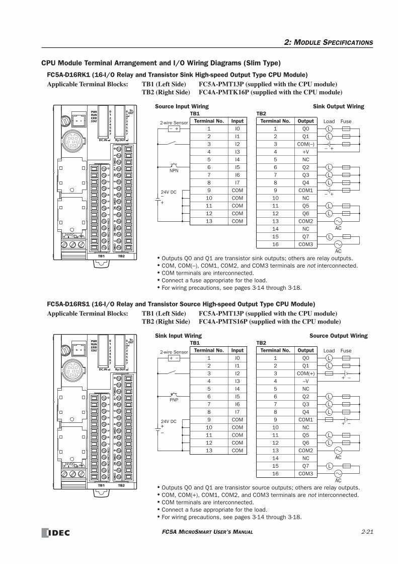
2: MODULE SPECIFICATIONS
CPU Module Terminal Arrangement and I/O Wiring Diagrams (Slim Type)
FC5A-D16RK1 (16-I/O Relay and Transistor Sink High-speed Output Type CPU Module)Applicable Terminal Blocks: TB1 (Left Side) FC5A-PMT13P (supplied with the CPU module)
TB2 (Right Side) FC4A-PMTK16P (supplied with the CPU module)
FC5A-D16RS1 (16-I/O Relay and Transistor Source High-speed Output Type CPU Module)Applicable Terminal Blocks: TB1 (Left Side) FC5A-PMT13P (supplied with the CPU module)
TB2 (Right Side) FC4A-PMTS16P (supplied with the CPU module)
+ –24VDC
TB1 TB2Terminal No. Input Terminal No. Output
1 I0 1 Q02 I1 2 Q13 I2 3 COM(–)4 I3 4 +V5 I4 5 NC6 I5 6 Q27 I6 7 Q38 I7 8 Q49 COM 9 COM1
10 COM 10 NC11 COM 11 Q512 COM 12 Q613 COM 13 COM2
14 NC15 Q716 COM3
Source Input Wiring
+–
+–2-wire Sensor
24V DC
NPN
Sink Output Wiring
LL
L
+–
L
LoadL
Fuse
AC
L
LL
+–
AC• Outputs Q0 and Q1 are transistor sink outputs; others are relay outputs.• COM, COM(–), COM1, COM2, and COM3 terminals are not interconnected.• COM terminals are interconnected.• Connect a fuse appropriate for the load.• For wiring precautions, see pages 3-14 through 3-18.
+ –24VDC
TB1 TB2Terminal No. Input Terminal No. Output
1 I0 1 Q02 I1 2 Q13 I2 3 COM(+)4 I3 4 –V5 I4 5 NC6 I5 6 Q27 I6 7 Q38 I7 8 Q49 COM 9 COM1
10 COM 10 NC11 COM 11 Q512 COM 12 Q613 COM 13 COM2
14 NC15 Q716 COM3
Sink Input Wiring
+–
+ –2-wire Sensor
24V DC
PNP
Source Output Wiring
LL
L
+ –
L
LoadL
Fuse
AC
L
LL
+ –
AC• Outputs Q0 and Q1 are transistor source outputs; others are relay outputs.• COM, COM(+), COM1, COM2, and COM3 terminals are not interconnected.• COM terminals are interconnected.• Connect a fuse appropriate for the load.• For wiring precautions, see pages 3-14 through 3-18.
FC5A MICROSMART USER’S MANUAL 2-21
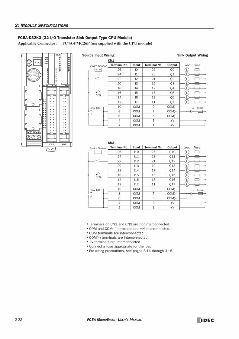
2: MODULE SPECIFICATIONS
FC5A-D32K3 (32-I/O Transistor Sink Output Type CPU Module)Applicable Connector: FC4A-PMC26P (not supplied with the CPU module)
+ –24VDC
CN1Terminal No. Input Terminal No. Output
26 I0 25 Q024 I1 23 Q122 I2 21 Q220 I3 19 Q318 I4 17 Q416 I5 15 Q514 I6 13 Q612 I7 11 Q710 COM 9 COM(–)8 COM 7 COM(–)6 COM 5 COM(–)4 COM 3 +V2 COM 1 +V
Source Input Wiring
+–
+–2-wire Sensor
24V DC
NPN
Sink Output Wiring
L
Fuse
L
L
+–
LLLL
LoadL
Fuse
CN2Terminal No. Input Terminal No. Output
26 I10 25 Q1024 I11 23 Q1122 I12 21 Q1220 I13 19 Q1318 I14 17 Q1416 I15 15 Q1514 I16 13 Q1612 I17 11 Q1710 COM 9 COM(–)8 COM 7 COM(–)6 COM 5 COM(–)4 COM 3 +V2 COM 1 +V
+–2-wire Sensor
NPNL
Fuse
L
L
+–
LLLL
LoadL
Fuse
• Terminals on CN1 and CN2 are not interconnected.• COM and COM(–) terminals are not interconnected.• COM terminals are interconnected.• COM(–) terminals are interconnected.• +V terminals are interconnected.• Connect a fuse appropriate for the load.• For wiring precautions, see pages 3-14 through 3-18.
+–24V DC
2-22 FC5A MICROSMART USER’S MANUAL

2: MODULE SPECIFICATIONS
FC5A-D32S3 (32-I/O Transistor Source Output Type CPU Module)Applicable Connector: FC4A-PMC26P (not supplied with the CPU module)
CN1Terminal No. Input Terminal No. Output
26 I0 25 Q024 I1 23 Q122 I2 21 Q220 I3 19 Q318 I4 17 Q416 I5 15 Q514 I6 13 Q612 I7 11 Q710 COM 9 COM(+)8 COM 7 COM(+)6 COM 5 COM(+)4 COM 3 –V2 COM 1 –V
Sink Input Wiring
+–
+ –2-wire Sensor
24V DC
PNP
Source Output Wiring
L
Fuse
L
L
+ –
LLLL
LoadL
Fuse
CN2Terminal No. Input Terminal No. Output
26 I10 25 Q1024 I11 23 Q1122 I12 21 Q1220 I13 19 Q1318 I14 17 Q1416 I15 15 Q1514 I16 13 Q1612 I17 11 Q1710 COM 9 COM(+)8 COM 7 COM(+)6 COM 5 COM(+)4 COM 3 –V2 COM 1 –V
+ –2-wire Sensor
PNPL
Fuse
L
L
+ –
LLLL
LoadL
Fuse
+ –24VDC
• Terminals on CN1 and CN2 are not interconnected.• COM and COM(+) terminals are not interconnected.• COM terminals are interconnected.• COM(+) terminals are interconnected.• –V terminals are interconnected.• Connect a fuse appropriate for the load.• For wiring precautions, see pages 3-14 through 3-18.
+–
24V DC
FC5A MICROSMART USER’S MANUAL 2-23

2: MODULE SPECIFICATIONS
Input ModulesDigital input modules are available in 8-, 16-, and 32-point DC input modules and an 8-point AC input module with a screw terminal block or plug-in connector for input wiring. All DC input modules accept both sink and source DC input signals.
The input modules can be connected to the all-in-one 24-I/O type CPU module and all slim type CPU modules to expand input terminals. The all-in-one 10- and 16-I/O type CPU modules cannot connect input modules.
Input Module Type Numbers
Parts Description
(1) Expansion Connector Connects to the CPU and other I/O modules. (The all-in-one 10- and 16-I/O type CPU modules cannot be connected.)
(2) Module Label Indicates the input module Type No. and specifications.
(3) LED Indicator Turns on when a corresponding input is on.
(4) Terminal No. Indicates terminal numbers.
(5) Cable Terminal/Connector Five different terminal/connector styles are available for wiring.
Module Name 8-point DC Input 16-point DC Input 32-point DC Input 8-point AC Input
Screw Terminal FC4A-N08B1 FC4A-N16B1 — FC4A-N08A11
Connector — FC4A-N16B3 FC4A-N32B3 —
The above figures illustrate the 8-point DC input module.
(1) Expansion Connector
(2) Module Label
(3) LED Indicator
(4) Terminal No.
(5) Cable Terminal/Connector
2-24 FC5A MICROSMART USER’S MANUAL

2: MODULE SPECIFICATIONS
DC Input Module Specifications
Type No. FC4A-N08B1 FC4A-N16B1 FC4A-N16B3 FC4A-N32B3
Input Points and Common Lines8 points in 1 common line
16 points in 1 common line
16 points in 1 common line
32 points in 2 common lines
Terminal Arrangement See Input Module Terminal Arrangement on pages 2-27 through 2-29.
Rated Input Voltage 24V DC sink/source input signal
Input Voltage Range 20.4 to 28.8V DC
Rated Input Current 7 mA/point (24V DC) 5 mA/point (24V DC)
Input Impedance 3.4 kΩ 4.4 kΩ
Turn ON Time (24V DC) 4 ms
Turn OFF Time (24V DC) 4 ms
IsolationBetween input terminals: Not isolated Internal circuit: Photocoupler isolated
External Load for I/O Interconnection Not needed
Signal Determination Method Static
Effect of Improper Input ConnectionBoth sinking and sourcing input signals can be connected. If any input exceeding the rated value is applied, permanent damage may be caused.
Cable Length 3m (9.84 ft.) in compliance with electromagnetic immunity
Connector on Mother Board MC1.5/10-G-3.81BK (Phoenix Contact) FL20A2MA (Oki Electric Cable)
Connector Insertion/Removal Durability 100 times minimum
Internal Current DrawAll Inputs ON
25 mA (5V DC) 0 mA (24V DC)
40 mA (5V DC) 0 mA (24V DC)
35 mA (5V DC) 0 mA (24V DC)
65 mA (5V DC) 0 mA (24V DC)
All Inputs OFF5 mA (5V DC) 0 mA (24V DC)
5 mA (5V DC) 0 mA (24V DC)
5 mA (5V DC) 0 mA (24V DC)
10 mA (5V DC) 0 mA (24V DC)
Weight 85g 100g 65g 100g
Input Internal Circuit
Input Usage LimitsWhen using the FC4A-N16B1 at 55°C in the normal mounting direction, limit the inputs which turn on simultaneously along line (1). At 45°C, all inputs can be turned on simultaneously at 28.8V DC as indicated with line (2).
When using the FC4A-N16B3 or -N32B3 at 55°C, limit the inputs which turn on simultaneously on each connector along line (3). At 30°C, all inputs can be turned on simultaneously at 28.8V DC as indicated with line (4).
When using the FC4A-N08B1, all inputs can be turned on simultaneously at 55°C, input voltage 28.8V DC.
FC4A-N08B1 and FC4A-N16B1 FC4A-N16B3 and FC4A-N32B3
Input
Inte
rnal
Circ
uit
COM
3.3 kΩInput
Inte
rnal
Circ
uit
COM
4.3 kΩ
Inpu
t Vo
ltag
e (V
DC
)
28.8
0100
Input Simultaneous ON Ratio (%)
26.4
(2) 45°C
(1) 55°C
700
Inpu
t Vo
ltag
e (V
DC
)
28.8
0100
Input Simultaneous ON Ratio (%)
26.4
(4) 30°C
90
(3) 55°C
700
24.0
50
Input Operating RangeThe input operating range of the Type 1 (IEC 61131-2) input module is shown below:
FC4A-N16B3 and FC4A-N32B3
Transition
OFF AreaInpu
t Vo
ltage
(V
DC
)
28.8
15
5
01.2 8.4
Input Current (mA)
ON Area
Area
7.04.2
24
FC4A-N08B1 and FC4A-N16B1
Transition
OFF AreaInpu
t Vo
ltage
(V
DC
)
28.8
15
5
00.9 6.4
Input Current (mA)
ON Area
Area
5.33.2
24
FC5A MICROSMART USER’S MANUAL 2-25

2: MODULE SPECIFICATIONS
AC Input Module Specifications
Type No. FC4A-N08A11
Input Points and Common Lines 8 points in 2 common lines
Terminal Arrangement See Input Module Terminal Arrangement on page 2-30.
Rated Input Voltage 100 to 120V AC (50/60 Hz)
Input Voltage Range 85 to 132V AC
Rated Input Current 17 mA/point (120V AC, 60 Hz)
Input Type AC input; Type 1, 2 (IEC 61131)
Input Impedance 0.8 kΩ (60 Hz)
Turn ON Time 25 ms
Turn OFF Time 30 ms
IsolationBetween input terminals in the same common: Not isolated Between input terminals in different commons: Isolated Between input terminals and internal circuits: Photocoupler isolated
External Load for I/O Interconnection Not needed
Signal Determination Method Static
Effect of Improper Input ConnectionIf any input exceeding the rated value is applied, permanent damage may be caused.
Connector on Mother Board MC1.5/11-G-3.81BK (Phoenix Contact)
Connector Insertion/Removal Durability 100 times minimum
Internal Current DrawAll Inputs ON
60 mA (5V DC) 0 mA (24V DC)
All Inputs OFF30 mA (5V DC) 0 mA (24V DC)
Weight 80g
Input Internal Circuit
Input Usage LimitsWhen using the FC4A-N08A11, all inputs can be turned on simultaneously at 55°C, input voltage 132V AC.
FC4A-N08A11
InputIn
tern
al C
ircui
t
COM
Inpu
t Vo
ltag
e (V
AC
)
132
0100
Input Simultaneous ON Ratio (%)
55°C
500
102
120
Input Operating RangeThe input operating range of the Type 1 and 2 (IEC 61131-2) input module is shown below:
FC4A-N08A11
74
20
01
Input Current (mA)5
132
Inpu
t Vo
ltage
(V
AC)
2 4 17
79
Transition
OFF Area
ON Area
100
13
Area
2-26 FC5A MICROSMART USER’S MANUAL

2: MODULE SPECIFICATIONS
DC Input Module Terminal Arrangement and Wiring Diagrams
FC4A-N08B1 (8-point DC Input Module) — Screw Terminal TypeApplicable Terminal Block: FC4A-PMT10P (supplied with the input module)
FC4A-N16B1 (16-point DC Input Module) — Screw Terminal TypeApplicable Terminal Block: FC4A-PMT10P (supplied with the input module)
COM
COM
01234567
DC.IN
01
23
45
67
Terminal No. Input0 I01 I12 I23 I34 I45 I56 I67 I7
COM COMCOM COM
Source Input WiringTerminal No. Input
0 I01 I12 I23 I34 I45 I56 I67 I7
COM COMCOM COM
Sink Input Wiring
• Two COM terminals are interconnected.• For input wiring precautions, see page 3-14.
+–
+–2-wire Sensor
24V DC
NPN
+–
+ –2-wire Sensor
24V DC
PNP
01234567
1011121314151617
DC.IN
COM
COM
1011
1213
1415
1617
0
1
2
3
4
5
6
7CO
MCO
M
Terminal No. Input0 I01 I12 I23 I34 I45 I56 I67 I7
COM COMCOM COM
10 I1011 I1112 I1213 I1314 I1415 I1516 I1617 I17
COM COMCOM COM
Source Input WiringTerminal No. Input
0 I01 I12 I23 I34 I45 I56 I67 I7
COM COMCOM COM
10 I1011 I1112 I1213 I1314 I1415 I1516 I1617 I17
COM COMCOM COM
Sink Input Wiring
• Four COM terminals are interconnected.• For input wiring precautions, see page 3-14.
+–
+–2-wire Sensor
24V DC
NPN
+–
NPN
+–
+ –2-wire Sensor
24V DC
PNP
+ –
PNP
FC5A MICROSMART USER’S MANUAL 2-27
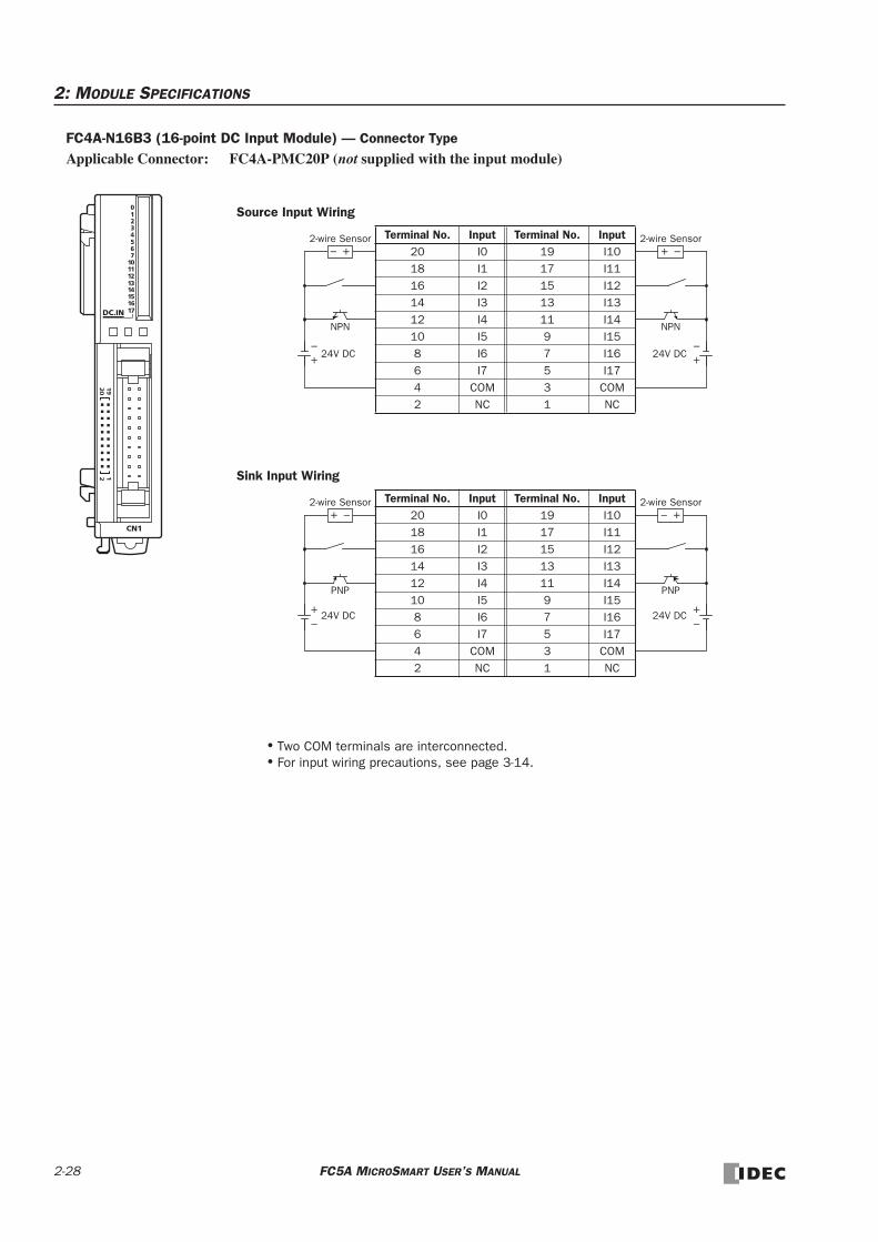
2: MODULE SPECIFICATIONS
FC4A-N16B3 (16-point DC Input Module) — Connector TypeApplicable Connector: FC4A-PMC20P (not supplied with the input module)
• Two COM terminals are interconnected.• For input wiring precautions, see page 3-14.
Terminal No. Input Terminal No. Input20 I0 19 I1018 I1 17 I1116 I2 15 I1214 I3 13 I1312 I4 11 I1410 I5 9 I158 I6 7 I166 I7 5 I174 COM 3 COM2 NC 1 NC
Source Input Wiring
+–
+–2-wire Sensor
24V DC
NPN
+–
+ –2-wire Sensor
24V DC
NPN
Terminal No. Input Terminal No. Input20 I0 19 I1018 I1 17 I1116 I2 15 I1214 I3 13 I1312 I4 11 I1410 I5 9 I158 I6 7 I166 I7 5 I174 COM 3 COM2 NC 1 NC
Sink Input Wiring
+–
+ –2-wire Sensor
24V DC
PNP
+–
+–2-wire Sensor
24V DC
PNP
2-28 FC5A MICROSMART USER’S MANUAL

2: MODULE SPECIFICATIONS
FC4A-N32B3 (32-point DC Input Module) — Connector TypeApplicable Connector: FC4A-PMC20P (not supplied with the input module)
CN1No. Input No. Input20 I0 19 I1018 I1 17 I1116 I2 15 I1214 I3 13 I1312 I4 11 I1410 I5 9 I158 I6 7 I166 I7 5 I174 COM0 3 COM02 NC 1 NC
Source Input Wiring
• COM0 terminals are interconnected.• COM1 terminals are interconnected.• COM0 and COM1 terminals are not interconnected.• For input wiring precautions, see page 3-14.
+–
+–2-wire Sensor
24V DC
NPN
+–
+ –2-wire Sensor
24V DC
NPN
CN2No. Input No. Input20 I20 19 I3018 I21 17 I3116 I22 15 I3214 I23 13 I3312 I24 11 I3410 I25 9 I358 I26 7 I366 I27 5 I374 COM1 3 COM12 NC 1 NC
+–
+–2-wire Sensor
24V DC
NPN
+–
+ –2-wire Sensor
24V DC
NPN
CN1No. Input No. Input20 I0 19 I1018 I1 17 I1116 I2 15 I1214 I3 13 I1312 I4 11 I1410 I5 9 I158 I6 7 I166 I7 5 I174 COM0 3 COM02 NC 1 NC
Sink Input Wiring
+–
+ –2-wire Sensor
24V DC
PNP
+–
+–2-wire Sensor
24V DC
PNP
CN2No. Input No. Input20 I20 19 I3018 I21 17 I3116 I22 15 I3214 I23 13 I3312 I24 11 I3410 I25 9 I358 I26 7 I366 I27 5 I374 COM1 3 COM12 NC 1 NC
+–
+ –2-wire Sensor
24V DC
PNP
+–
+–2-wire Sensor
24V DC
PNP
FC5A MICROSMART USER’S MANUAL 2-29

2: MODULE SPECIFICATIONS
AC Input Module Terminal Arrangement and Wiring Diagrams
FC4A-N08A11 (8-point AC Input Module) — Screw Terminal TypeApplicable Terminal Block: FC4A-PMT11P (supplied with the input module)
7CO
M1
01234567
AC.IN
10
23
COM
0N
C4
56
Terminal No. Output0 I01 I12 I23 I3
COM0 COM0NC NC4 I45 I56 I67 I7
COM1 COM1
AC
AC
• Two COM terminals are not interconnected.• For input wiring precautions, see page 3-14.• Do not connect an external load to the input terminals.
2-30 FC5A MICROSMART USER’S MANUAL

2: MODULE SPECIFICATIONS
Output ModulesDigital output modules are available in 8- and 16-point relay output modules, 8-, 16- and 32-point transistor sink output modules, and 8-, 16- and 32-point transistor source output modules with a screw terminal block or plug-in connector for output wiring.
The output modules can be connected to the all-in-one 24-I/O type CPU module and all slim type CPU modules to expand output terminals. The all-in-one 10- and 16-I/O type CPU modules cannot connect output modules.
Output Module Type Numbers
Parts Description
(1) Expansion Connector Connects to the CPU and other I/O modules. (The all-in-one 10- and 16-I/O type CPU modules cannot be connected.)
(2) Module Label Indicates the output module Type No. and specifications.
(3) LED Indicator Turns on when a corresponding output is on.
(4) Terminal No. Indicates terminal numbers.
(5) Cable Terminal/Connector Five different terminal/connector styles are available for wiring.
Module Name Terminal Type No.
8-point Relay Output
Removable Terminal Block
FC4A-R081
16-point Relay Output FC4A-R161
8-point Transistor Sink Output FC4A-T08K1
8-point Transistor Source Output FC4A-T08S1
16-point Transistor Sink Output
MIL Connector
FC4A-T16K3
16-point Transistor Source Output FC4A-T16S3
32-point Transistor Sink Output FC4A-T32K3
32-point Transistor Source Output FC4A-T32S3
The above figures illustrate the 8-point relay output module.
(1) Expansion Connector
(2) Module Label
(3) LED Indicator
(4) Terminal No.
(5) Cable Terminal/Connector
FC5A MICROSMART USER’S MANUAL 2-31

2: MODULE SPECIFICATIONS
Relay Output Module Specifications
Note: When relay output modules are connected to the all-in-one 24-I/O type CPU module or any slim type CPU module, the maximum number of relay outputs that can be turned on simultaneously, including the outputs on the CPU module, are shown below.
Output Delay
Type No. FC4A-R081 FC4A-R161
Output Points and Common Lines 8 NO contacts in 2 common lines 16 NO contacts in 2 common lines
Terminal Arrangement See Relay Output Module Terminal Arrangement on page 2-33.
Maximum Load Current2A per point
7A per common line 8A per common line
Minimum Switching Load 0.1 mA/0.1V DC (reference value)
Initial Contact Resistance 30 mΩ maximum
Electrical Life 100,000 operations minimum (rated load 1,800 operations/hour)
Mechanical Life 20,000,000 operations minimum (no load 18,000 operations/hour)
Rated Load240V AC/2A (resistive load, inductive load cos ø = 0.4) 30V DC/2A (resistive load, inductive load L/R = 7 ms)
Dielectric StrengthBetween output and or terminals: 1,500V AC, 1 minute Between output terminal and internal circuit: 1,500V AC, 1 minute Between output terminals (COMs): 1,500V AC, 1 minute
Connector on Mother BoardMC1.5/11-G-3.81BK (Phoenix Contact)
MC1.5/10-G-3.81BK (Phoenix Contact)
Connector Insertion/Removal Durability 100 times minimum 100 times minimum
Internal Current DrawAll Outputs ON
30 mA (5V DC) 40 mA (24V DC)
45 mA (5V DC) 75 mA (24V DC)
All Outputs OFF5 mA (5V DC) 0 mA (24V DC)
5 mA (5V DC) 0 mA (24V DC)
Internal Power Consumption(at 24V DC while all outputs ON)
1.16W 2.10W
Weight 110g 145g
Contact Protection Circuit for Relay Output See page 3-16.
CPU Module TypeAll-in-One 24-I/O CPU Module
Slim Type CPU ModuleAC Power Type DC Power Type
Maximum Relay Outputs Turning On Simultaneously
33 44108 total
54 (on the left of expansion interface module)54 (on the right of expansion interface module)
Command
Output Relay Status
OFF delay: 10 ms maximum
Chatter: 6 ms maximum
ON delay: 6 ms maximum
ON
OFF
ON
OFF
2-32 FC5A MICROSMART USER’S MANUAL

2: MODULE SPECIFICATIONS
Relay Output Module Terminal Arrangement and Wiring Diagrams
FC4A-R081 (8-point Relay Output Module) — Screw Terminal TypeApplicable Terminal Block: FC4A-PMT11P (supplied with the output module)
FC4A-R161 (16-point Relay Output Module) — Screw Terminal TypeApplicable Terminal Block: FC4A-PMT10P (supplied with the output module)
L
7CO
M1
01234567
Ry.OUT
10
23
COM
0N
C4
56
Terminal No. Output0 Q01 Q12 Q23 Q3
COM0 COM0NC NC4 Q45 Q56 Q67 Q7
COM1 COM1
L
Fuse
LL
L
AC
Fuse
Fuse
DC
DC
LoadL
LL
Fuse+–
AC
Fuse
Fuse
DC
DC+–
+–
+–
• COM0 and COM1 terminals are not interconnected.• Connect a fuse appropriate for the load.• For output wiring precautions, see page 3-15.
Fuse
01234567
1011121314151617
Ry.OUT
COM
1CO
M1
1011
1213
1415
1617
0
1
2
3
4
5
6
7CO
M0
COM
0
L
Terminal No. Output0 Q01 Q12 Q23 Q34 Q45 Q56 Q67 Q7
COM0 COM0COM0 COM0
10 Q1011 Q1112 Q1213 Q1314 Q1415 Q1516 Q1617 Q17
COM1 COM1COM1 COM1
L
Fuse+–
LL
LAC
Fuse
Fuse
DC
DC+–
LoadL
LL
L
L
Fuse+–
LL
LAC
Fuse
Fuse
DC
DC+–
L
LL
• COM0 terminals are interconnected.• COM1 terminals are interconnected.• COM0 and COM1 terminals are not interconnected.• Connect a fuse appropriate for the load.• For output wiring precautions, see page 3-15.
Fuse
FC5A MICROSMART USER’S MANUAL 2-33

2: MODULE SPECIFICATIONS
Transistor Sink Output Module Specifications
Output Internal Circuit
Type No. FC4A-T08K1 FC4A-T16K3 FC4A-T32K3
Output Type Transistor sink output
Output Points and Common Lines8 points in 1 common line
16 points in 1 common line
32 points in 2 common lines
Terminal ArrangementSee Transistor Sink Output Module Terminal Arrangement on pages 2-35 and 2-36.
Rated Load Voltage 24V DC
Operating Load Voltage Range 20.4 to 28.8V DC
Rated Load Current 0.3A per output point 0.1A per output point
Maximum Load Current (at 28.8V DC)0.3A per output point 3A per common line
0.1A per output point 1A per common line
Voltage Drop (ON Voltage) 1V maximum (voltage between COM and output terminals when output is on)
Inrush Current 1A maximum
Leakage Current 0.1 mA maximum
Clamping Voltage 39V±1V
Maximum Lamp Load 8W
Inductive Load L/R = 10 ms (28.8V DC, 1 Hz)
External Current Draw 100 mA maximum, 24V DC (power voltage at the +V terminal)
IsolationBetween output terminal and internal circuit: Photocoupler isolated Between output terminals: Not isolated
Connector on Mother BoardMC1.5/10-G-3.81BK (Phoenix Contact)
FL20A2MA (Oki Electric Cable)
Connector Insertion/Removal Durability 100 times minimum
Internal Current Draw
All Outputs ON10 mA (5V DC) 20 mA (24V DC)
10 mA (5V DC) 40 mA (24V DC)
20 mA (5V DC) 70 mA (24V DC)
All Outputs OFF5 mA (5V DC) 0 mA (24V DC)
5 mA (5V DC) 0 mA (24V DC)
10 mA (5V DC) 0 mA (24V DC)
Internal Power Consumption(at 24V DC while all outputs ON)
0.55W 1.03W 1.82W
Output DelayTurn ON time: 300 µs maximum Turn OFF time: 300 µs maximum
Weight (approx.) 85g 70g 105g
+V
Output
Inte
rnal
Circ
uit
COM(–)
Sink Output
2-34 FC5A MICROSMART USER’S MANUAL

2: MODULE SPECIFICATIONS
Transistor Sink Output Module Terminal Arrangement and Wiring Diagrams
FC4A-T08K1 (8-point Transistor Sink Output Module) — Screw Terminal TypeApplicable Terminal Block: FC4A-PMT10P (supplied with the output module)
FC4A-T16K3 (16-point Transistor Sink Output Module) — Connector TypeApplicable Connector: FC4A-PMC20P (not supplied with the output module)
L
Terminal No. Output0 Q01 Q12 Q23 Q34 Q45 Q56 Q67 Q7
COM(–) COM(–)+V +V
Fuse L
L
+ –
LLLL
LoadL
COM
(–)+
V
01234567
Tr.OUT
01
23
45
67
• Connect a fuse appropriate for the load.• For output wiring precautions, see page 3-15.
Fuse
• COM(–) terminals are interconnected.• +V terminals are interconnected.• Connect a fuse appropriate for the load.• For output wiring precautions, see page 3-15.
Terminal No. Output Terminal No. Output20 Q0 19 Q1018 Q1 17 Q1116 Q2 15 Q1214 Q3 13 Q1312 Q4 11 Q1410 Q5 9 Q158 Q6 7 Q166 Q7 5 Q174 COM(–) 3 COM(–)2 +V 1 +V
LL
L
+–
LLLL
LoadL
Fuse
LL
L
+ –
LLLL
LoadL
Fuse
FC5A MICROSMART USER’S MANUAL 2-35
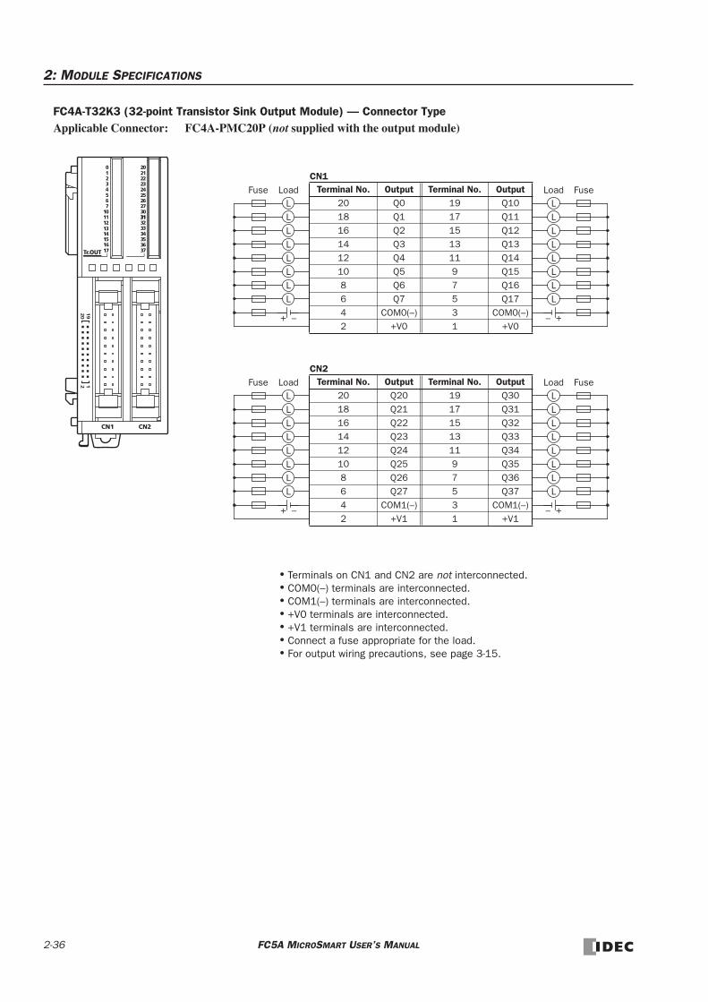
2: MODULE SPECIFICATIONS
FC4A-T32K3 (32-point Transistor Sink Output Module) — Connector TypeApplicable Connector: FC4A-PMC20P (not supplied with the output module)
• Terminals on CN1 and CN2 are not interconnected.• COM0(–) terminals are interconnected.• COM1(–) terminals are interconnected.• +V0 terminals are interconnected.• +V1 terminals are interconnected.• Connect a fuse appropriate for the load.• For output wiring precautions, see page 3-15.
CN1Terminal No. Output Terminal No. Output
20 Q0 19 Q1018 Q1 17 Q1116 Q2 15 Q1214 Q3 13 Q1312 Q4 11 Q1410 Q5 9 Q158 Q6 7 Q166 Q7 5 Q174 COM0(–) 3 COM0(–)2 +V0 1 +V0
LL
L
+–
LLLL
LoadL
Fuse
LL
L
+ –
LLLL
LoadL
Fuse
CN2Terminal No. Output Terminal No. Output
20 Q20 19 Q3018 Q21 17 Q3116 Q22 15 Q3214 Q23 13 Q3312 Q24 11 Q3410 Q25 9 Q358 Q26 7 Q366 Q27 5 Q374 COM1(–) 3 COM1(–)2 +V1 1 +V1
LL
L
+–
LLLL
LoadL
Fuse
LL
L
+ –
LLLL
LoadL
Fuse
2-36 FC5A MICROSMART USER’S MANUAL

2: MODULE SPECIFICATIONS
Transistor Source Output Module Specifications
Output Internal Circuit
Type No. FC4A-T08S1 FC4A-T16S3 FC4A-T32S3
Output Type Transistor source output
Output Points and Common Lines8 points in 1 common line
16 points in 1 common line
32 points in 2 common lines
Terminal ArrangementSee Transistor Source Output Module Terminal Arrangement on pages 2-38 and 2-39.
Rated Load Voltage 24V DC
Operating Load Voltage Range 20.4 to 28.8V DC
Rated Load Current 0.3A per output point 0.1A per output point
Maximum Load Current (at 28.8V DC)0.3A per output point 3A per common line
0.1A per output point 1A per common line
Voltage Drop (ON Voltage) 1V maximum (voltage between COM and output terminals when output is on)
Inrush Current 1A maximum
Leakage Current 0.1 mA maximum
Clamping Voltage 39V±1V
Maximum Lamp Load 8W
Inductive Load L/R = 10 ms (28.8V DC, 1 Hz)
External Current Draw 100 mA maximum, 24V DC (power voltage at the –V terminal)
IsolationBetween output terminal and internal circuit: Photocoupler isolated Between output terminals: Not isolated
Connector on Mother BoardMC1.5/10-G-3.81BK (Phoenix Contact)
FL20A2MA (Oki Electric Cable)
Connector Insertion/Removal Durability 100 times minimum
Internal Current Draw
All Outputs ON10 mA (5V DC) 20 mA (24V DC)
10 mA (5V DC) 40 mA (24V DC)
20 mA (5V DC) 70 mA (24V DC)
All Outputs OFF5 mA (5V DC) 0 mA (24V DC)
5 mA (5V DC) 0 mA (24V DC)
10 mA (5V DC) 0 mA (24V DC)
Internal Power Consumption(at 24V DC while all outputs ON)
0.55W 1.03W 1.82W
Output DelayTurn ON time: 300 µs maximum Turn OFF time: 300 µs maximum
Weight (approx.) 85g 70g 105g
COM(+)
Output
Inte
rnal
Circ
uit
–V
Source Output
FC5A MICROSMART USER’S MANUAL 2-37

2: MODULE SPECIFICATIONS
Transistor Source Output Module Terminal Arrangement and Wiring Diagrams
FC4A-T08S1 (8-point Transistor Source Output Module) — Screw Terminal TypeApplicable Terminal Block: FC4A-PMT10P (supplied with the output module)
FC4A-T16S3 (16-point Transistor Source Output Module) — Connector TypeApplicable Connector: FC4A-PMC20P (not supplied with the output module)
COM
(+)–V
01234567
Tr.OUT
01
23
45
67
L
Terminal No. Output0 Q01 Q12 Q23 Q34 Q45 Q56 Q67 Q7
COM(+) COM(+)–V –V
Fuse L
L
+–
LLLL
LoadL
• Connect a fuse appropriate for the load.• For output wiring precautions, see page 3-15.
• COM(+) terminals are interconnected.• –V terminals are interconnected.• Connect a fuse appropriate for the load.• For output wiring precautions, see page 3-15.
Terminal No. Output Terminal No. Output20 Q0 19 Q1018 Q1 17 Q1116 Q2 15 Q1214 Q3 13 Q1312 Q4 11 Q1410 Q5 9 Q158 Q6 7 Q166 Q7 5 Q174 COM(+) 3 COM(+)2 –V 1 –V
LL
L
+ –
LLLL
LoadL
Fuse
LL
L
+–
LLLL
LoadL
Fuse
2-38 FC5A MICROSMART USER’S MANUAL

2: MODULE SPECIFICATIONS
FC4A-T32S3 (32-point Transistor Source Output Module) — Connector TypeApplicable Connector: FC4A-PMC20P (not supplied with the output module)
• Terminals on CN1 and CN2 are not interconnected.• COM0(+) terminals are interconnected.• COM1(+) terminals are interconnected.• –V0 terminals are interconnected.• –V1 terminals are interconnected.• Connect a fuse appropriate for the load.• For output wiring precautions, see page 3-15.
CN1Terminal No. Output Terminal No. Output
20 Q0 19 Q1018 Q1 17 Q1116 Q2 15 Q1214 Q3 13 Q1312 Q4 11 Q1410 Q5 9 Q158 Q6 7 Q166 Q7 5 Q174 COM0(+) 3 COM0(+)2 –V0 1 –V0
LL
L
+ –
LLLL
LoadL
Fuse
LL
L
+–
LLLL
LoadL
Fuse
CN2Terminal No. Output Terminal No. Output
20 Q20 19 Q3018 Q21 17 Q3116 Q22 15 Q3214 Q23 13 Q3312 Q24 11 Q3410 Q25 9 Q358 Q26 7 Q366 Q27 5 Q374 COM1(+) 3 COM1(+)2 –V1 1 –V1
LL
L
+ –
LLLL
LoadL
Fuse
LL
L
+–
LLLL
LoadL
Fuse
FC5A MICROSMART USER’S MANUAL 2-39

2: MODULE SPECIFICATIONS
Mixed I/O ModulesThe 4-in/4-out mixed I/O module has 4-point DC sink/source inputs and 4-point relay outputs, with a screw terminal block for I/O wiring. The 16-in/8-out mixed I/O module has 16-point DC sink/source inputs and 8-point relay outputs, with a wire-clamp terminal block for I/O wiring.
The mixed I/O modules can be connected to the all-in-one 24-I/O type CPU module and all slim type CPU modules to expand input and output terminals. The all-in-one 10- and 16-I/O type CPU modules cannot connect mixed I/O modules.
Mixed I/O Module Type Numbers
Parts Description
(1) Expansion Connector Connects to the CPU and other I/O modules. (The all-in-one 10- and 16-I/O type CPU modules cannot be connected.)
(2) Module Label Indicates the mixed I/O module Type No. and specifications.
(3) LED Indicator Turns on when a corresponding input or output is on.
(4) Terminal No. Indicates terminal numbers.
(5) Cable Terminal Two different terminal styles are available for wiring.
Module Name Terminal Type No.
4-in/4-out Mixed I/O Module Removable Terminal Block FC4A-M08BR1
16-in/8-out Mixed I/O Module Non-removable Wire-clamp Terminal Block FC4A-M24BR2
(1) Expansion Connector
(2) Module Label
(3) LED Indicator
(4) Terminal No.
(5) Cable Terminal
The above figures illustrate the 4-in/4-out mixed I/O module.
2-40 FC5A MICROSMART USER’S MANUAL
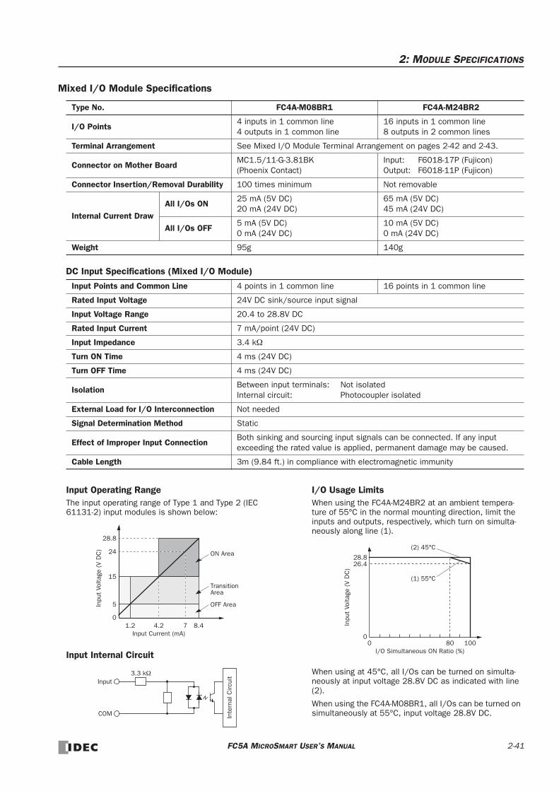
2: MODULE SPECIFICATIONS
Mixed I/O Module Specifications
DC Input Specifications (Mixed I/O Module)
Type No. FC4A-M08BR1 FC4A-M24BR2
I/O Points4 inputs in 1 common line 4 outputs in 1 common line
16 inputs in 1 common line 8 outputs in 2 common lines
Terminal Arrangement See Mixed I/O Module Terminal Arrangement on pages 2-42 and 2-43.
Connector on Mother BoardMC1.5/11-G-3.81BK (Phoenix Contact)
Input: F6018-17P (Fujicon) Output: F6018-11P (Fujicon)
Connector Insertion/Removal Durability 100 times minimum Not removable
Internal Current DrawAll I/Os ON
25 mA (5V DC) 20 mA (24V DC)
65 mA (5V DC) 45 mA (24V DC)
All I/Os OFF5 mA (5V DC) 0 mA (24V DC)
10 mA (5V DC) 0 mA (24V DC)
Weight 95g 140g
Input Points and Common Line 4 points in 1 common line 16 points in 1 common line
Rated Input Voltage 24V DC sink/source input signal
Input Voltage Range 20.4 to 28.8V DC
Rated Input Current 7 mA/point (24V DC)
Input Impedance 3.4 kΩ
Turn ON Time 4 ms (24V DC)
Turn OFF Time 4 ms (24V DC)
IsolationBetween input terminals: Not isolated Internal circuit: Photocoupler isolated
External Load for I/O Interconnection Not needed
Signal Determination Method Static
Effect of Improper Input ConnectionBoth sinking and sourcing input signals can be connected. If any input exceeding the rated value is applied, permanent damage may be caused.
Cable Length 3m (9.84 ft.) in compliance with electromagnetic immunity
Input Operating RangeThe input operating range of Type 1 and Type 2 (IEC 61131-2) input modules is shown below:
Input Internal Circuit
I/O Usage LimitsWhen using the FC4A-M24BR2 at an ambient tempera-ture of 55°C in the normal mounting direction, limit the inputs and outputs, respectively, which turn on simulta-neously along line (1).
When using at 45°C, all I/Os can be turned on simulta-neously at input voltage 28.8V DC as indicated with line (2).
When using the FC4A-M08BR1, all I/Os can be turned on simultaneously at 55°C, input voltage 28.8V DC.
Transition
OFF AreaInpu
t Vo
ltage
(V
DC
)
28.8
15
5
01.2 8.4
Input Current (mA)
ON Area
Area
74.2
24
Input
Inte
rnal
Circ
uit
COM
3.3 kΩ
Inpu
t Vo
ltage
(V
DC
)
28.8
0100
I/O Simultaneous ON Ratio (%)
26.4
(2) 45°C
80
(1) 55°C
0
FC5A MICROSMART USER’S MANUAL 2-41
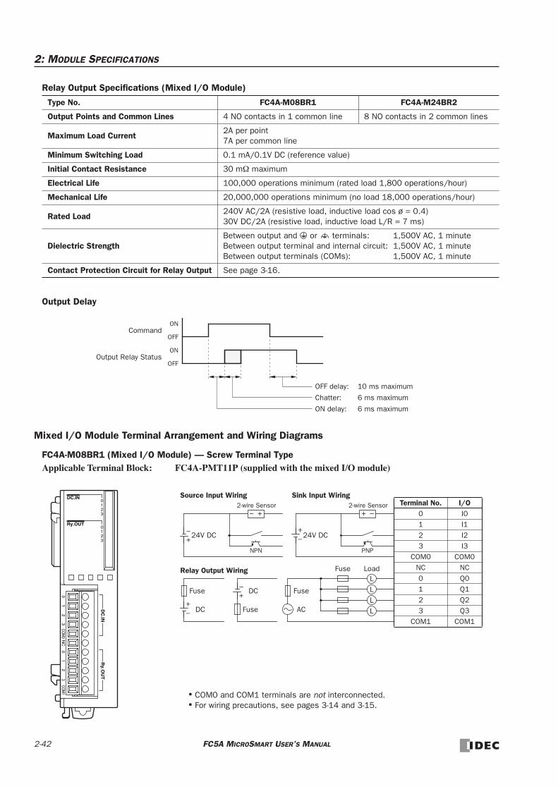
2: MODULE SPECIFICATIONS
Relay Output Specifications (Mixed I/O Module)
Output Delay
Mixed I/O Module Terminal Arrangement and Wiring Diagrams
FC4A-M08BR1 (Mixed I/O Module) — Screw Terminal TypeApplicable Terminal Block: FC4A-PMT11P (supplied with the mixed I/O module)
Type No. FC4A-M08BR1 FC4A-M24BR2
Output Points and Common Lines 4 NO contacts in 1 common line 8 NO contacts in 2 common lines
Maximum Load Current2A per point7A per common line
Minimum Switching Load 0.1 mA/0.1V DC (reference value)
Initial Contact Resistance 30 mΩ maximum
Electrical Life 100,000 operations minimum (rated load 1,800 operations/hour)
Mechanical Life 20,000,000 operations minimum (no load 18,000 operations/hour)
Rated Load240V AC/2A (resistive load, inductive load cos ø = 0.4) 30V DC/2A (resistive load, inductive load L/R = 7 ms)
Dielectric StrengthBetween output and or terminals: 1,500V AC, 1 minute Between output terminal and internal circuit: 1,500V AC, 1 minute Between output terminals (COMs): 1,500V AC, 1 minute
Contact Protection Circuit for Relay Output See page 3-16.
Command
Output Relay Status
OFF delay: 10 ms maximum
Chatter: 6 ms maximum
ON delay: 6 ms maximum
ON
OFF
ON
OFF
L
3CO
M1
0123
0123
DC.IN
Ry.OUT
10
23
COM
0N
C0
12
Ry.O
UT
DC
.IN
Terminal No. I/O0 I01 I12 I23 I3
COM0 COM0NC NC0 Q01 Q12 Q23 Q3
COM1 COM1
Fuse
L
AC
Fuse
Fuse
DC
DC
Load
LL
+–
+–
+–
Sink Input Wiring
• COM0 and COM1 terminals are not interconnected.• For wiring precautions, see pages 3-14 and 3-15.
FuseRelay Output Wiring
24V DC
+ –2-wire Sensor
PNP
+–
Source Input Wiring
24V DC
+–2-wire Sensor
NPN
2-42 FC5A MICROSMART USER’S MANUAL

2: MODULE SPECIFICATIONS
FC4A-M24BR2 (Mixed I/O Module) — Wire-clamp Terminal Type
Terminal No. Input1 I02 I13 I24 I35 I46 I57 I68 I79 I10
10 I1111 I1212 I1313 I1414 I1515 I1616 I1717 COM0
Source Input Wiring
Terminal No. Input1 I02 I13 I24 I35 I46 I57 I68 I79 I10
10 I1111 I1212 I1313 I1414 I1515 I1616 I1717 COM0
Sink Input Wiring
+–
+–2-wire Sensor
24V DC
NPN
+–
+ –2-wire Sensor
24V DC
PNP
L
Terminal No. Output1 Q02 Q13 Q24 Q35 COM16 NC7 Q48 Q59 Q6
10 Q711 COM2
L
Fuse
LL
L
AC
Fuse
Fuse
DC
DC
LoadL
LL
Fuse+–
AC
Fuse
Fuse
DC
DC+–
+–
+–
• COM0, COM1, and COM2 terminals are not interconnected.• Connect a fuse appropriate for the load.• For wiring precautions, see pages 3-14 and 3-15.
FuseRelay Output Wiring
FC5A MICROSMART USER’S MANUAL 2-43
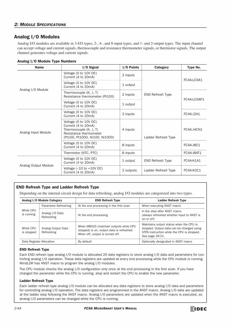
2: MODULE SPECIFICATIONS
Analog I/O ModulesAnalog I/O modules are available in 3-I/O types, 2-, 4-, and 8-input types, and 1- and 2-output types. The input channel can accept voltage and current signals, thermocouple and resistance thermometer signals, or thermistor signals. The output channel generates voltage and current signals.
Analog I/O Module Type Numbers
Name I/O Signal I/O Points Category Type No.
Analog I/O Module
Voltage (0 to 10V DC) Current (4 to 20mA) 2 inputs
END Refresh Type
FC4A-L03A1Voltage (0 to 10V DC) Current (4 to 20mA) 1 output
Thermocouple (K, J, T) Resistance thermometer (Pt100) 2 inputs
FC4A-L03AP1Voltage (0 to 10V DC) Current (4 to 20mA) 1 output
Analog Input Module
Voltage (0 to 10V DC) Current (4 to 20mA) 2 inputs FC4A-J2A1
Voltage (0 to 10V DC) Current (4 to 20mA) Thermocouple (K, J, T) Resistance thermometer (Pt100, Pt1000, Ni100, Ni1000)
4 inputs
Ladder Refresh Type
FC4A-J4CN1
Voltage (0 to 10V DC) Current (4 to 20mA) 8 inputs FC4A-J8C1
Thermistor (NTC, PTC) 8 inputs FC4A-J8AT1
Analog Output Module
Voltage (0 to 10V DC) Current (4 to 20mA) 1 output END Refresh Type FC4A-K1A1
Voltage (–10 to +10V DC) Current (4 to 20mA) 2 outputs Ladder Refresh Type FC4A-K2C1
END Refresh Type and Ladder Refresh TypeDepending on the internal circuit design for data refreshing, analog I/O modules are categorized into two types.
END Refresh TypeEach END refresh type analog I/O module is allocated 20 data registers to store analog I/O data and parameters for con-trolling analog I/O operation. These data registers are updated at every end processing while the CPU module is running. WindLDR has ANST macro to program the analog I/O modules.
The CPU module checks the analog I/O configuration only once at the end processing in the first scan. If you have changed the parameter while the CPU is running, stop and restart the CPU to enable the new parameter.
Ladder Refresh TypeEach ladder refresh type analog I/O module can be allocated any data registers to store analog I/O data and parameters for controlling analog I/O operation. The data registers are programmed in the ANST macro. Analog I/O data are updated at the ladder step following the ANST macro. Analog I/O parameters are updated when the ANST macro is executed, so analog I/O parameters can be changed while the CPU is running.
Analog I/O Module Category END Refresh Type Ladder Refresh Type
While CPU is running
Parameter Refreshing At the end processing in the first scan When executing ANST macro
Analog I/O Data Refreshing
At the end processingIn the step after ANST macro (always refreshed whether input to ANST is on or off)
While CPU is stopped
Analog Output Data Refreshing
When M8025 (maintain outputs while CPU stopped) is on, output data is refreshed. When off, output is turned off.
Maintains output status when the CPU is stopped. Output data can be changed using STPA instruction while the CPU is stopped. See page 26-21.
Data Register Allocation By default Optionally designated in ANST macro
2-44 FC5A MICROSMART USER’S MANUAL

2: MODULE SPECIFICATIONS
Parts Description
(1) Expansion Connector Connects to the CPU and other I/O modules. (The all-in-one 10- and 16-I/O type CPU modules cannot be connected.)
(2) Module Label Indicates the analog I/O module Type No. and specifications.
(3) Power LED (PWR) END refresh type FC4A-L03A1, FC4A-L03AP1, FC4A-J2A1, FC4A-K1A1: Turns on when power is supplied to the analog I/O module.
(3) Status LED (STAT) Ladder refresh type FC4A-J4CN1, FC4A-J8C1, FC4A-J8AT1, FC4A-K2C1: Indicates the operating status of the analog I/O module.
(4) Terminal No. Indicates terminal numbers.
(5) Cable Terminal All analog I/O modules have a removable terminal block.
Status LED Analog Input Operating Status
OFF Analog I/O module is stopped
ON Normal operation
Flash
InitializingChanging configurationHardware initialization errorExternal power supply error
The terminal style depends on the model of analog I/O modules.
(1) Expansion Connector
(2) Module Label
(3) Power LED (PWR)
(4) Terminal No.
(5) Cable Terminal
(3) Status LED (STAT)
FC5A MICROSMART USER’S MANUAL 2-45
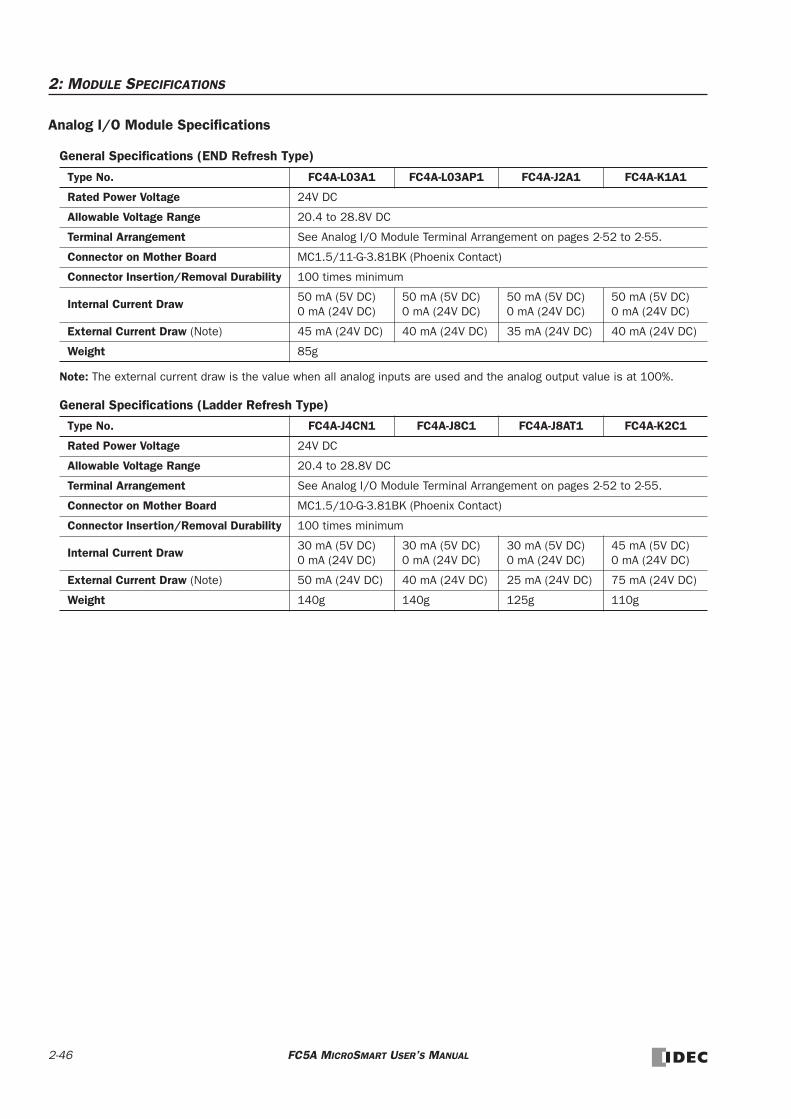
2: MODULE SPECIFICATIONS
Analog I/O Module Specifications
General Specifications (END Refresh Type)
Note: The external current draw is the value when all analog inputs are used and the analog output value is at 100%.
General Specifications (Ladder Refresh Type)
Type No. FC4A-L03A1 FC4A-L03AP1 FC4A-J2A1 FC4A-K1A1
Rated Power Voltage 24V DC
Allowable Voltage Range 20.4 to 28.8V DC
Terminal Arrangement See Analog I/O Module Terminal Arrangement on pages 2-52 to 2-55.
Connector on Mother Board MC1.5/11-G-3.81BK (Phoenix Contact)
Connector Insertion/Removal Durability 100 times minimum
Internal Current Draw50 mA (5V DC) 0 mA (24V DC)
50 mA (5V DC) 0 mA (24V DC)
50 mA (5V DC) 0 mA (24V DC)
50 mA (5V DC) 0 mA (24V DC)
External Current Draw (Note) 45 mA (24V DC) 40 mA (24V DC) 35 mA (24V DC) 40 mA (24V DC)
Weight 85g
Type No. FC4A-J4CN1 FC4A-J8C1 FC4A-J8AT1 FC4A-K2C1
Rated Power Voltage 24V DC
Allowable Voltage Range 20.4 to 28.8V DC
Terminal Arrangement See Analog I/O Module Terminal Arrangement on pages 2-52 to 2-55.
Connector on Mother Board MC1.5/10-G-3.81BK (Phoenix Contact)
Connector Insertion/Removal Durability 100 times minimum
Internal Current Draw30 mA (5V DC) 0 mA (24V DC)
30 mA (5V DC) 0 mA (24V DC)
30 mA (5V DC) 0 mA (24V DC)
45 mA (5V DC) 0 mA (24V DC)
External Current Draw (Note) 50 mA (24V DC) 40 mA (24V DC) 25 mA (24V DC) 75 mA (24V DC)
Weight 140g 140g 125g 110g
2-46 FC5A MICROSMART USER’S MANUAL

2: MODULE SPECIFICATIONS
Analog Input Specifications (END Refresh Type)
For Note 1 through Note 3, see page 2-51.
Type No. FC4A-L03A1 / FC4A-J2A1 FC4A-L03AP1
Analog Input Signal Type Voltage Input Current Input ThermocoupleResistance
Thermometer
Input Range 0 to 10V DC 4 to 20 mA DC
Type K (0 to 1300°C)Type J (0 to 1200°C)Type T (0 to 400°C)
Pt 100 3-wire type(–100 to 500°C)
Input Impedance 1 MΩ minimum 10Ω 1 MΩ minimum 1 MΩ minimumAllowable Conductor Resistance (per wire)
— — — 200Ω maximum
Input Detection Current — — — 1.0 mA maximumSample Duration Time 20 ms maximum 20 ms maximumSample Repetition Time 20 ms maximum 20 ms maximumTotal Input System Transfer Time 105 ms + 1 scan time (Note 1) 200 ms + 1 scan time (Note 1)
Type of InputSingle-ended input
Differential input
Operating Mode Self-scanConversion Method ∑∆ type ADC
Input Error
Maximum Error at 25°C ±0.2% of full scale
±0.2% of full scale plus reference junction compen-sation accuracy (±4°C maximum)
±0.2% of full scale
Temperature Coefficient ±0.006% of full scale/°CRepeatability after Stabilization Time
±0.5% of full scale
Non-lineality ±0.2% of full scaleMaximum Error ±1% of full scale
Digital Resolution 4096 increments (12 bits)
Input Value of LSB 2.5 mV 4 µAK: 0.325°C J: 0.300°C T: 0.100°C
0.15°C
Data Type in Application Program0 to 4095 (12-bit data) –32768 to 32767 (optional range designation) (Note 2)
Monotonicity YesInput Data Out of Range Detectable (Note 3)
Noise Resistance
Maximum Temporary Deviation during Electrical Noise Tests
±3% maximumAccuracy is not assured when noise is applied
Input Filter No
Recommended CableTwisted pair shielded cable is recom-mended for improved noise immunity
—
Crosstalk 2 LSB maximum
IsolationIsolated between input and power circuitPhotocoupler-isolated between input and internal circuit
Effect of Improper Input Connection No damageMaximum Permanent Allowed Overload (No Damage)
13V DC 40 mA DC —
Selection of Analog Input Signal Type Using software programmingCalibration or Verification to Maintain Rated Accuracy
Impossible
FC5A MICROSMART USER’S MANUAL 2-47

2: MODULE SPECIFICATIONS
Analog Input Specifications (Ladder Refresh Type)Type No. FC4A-J4CN1 / FC4A-J8C1 FC4A-J4CN1
Analog Input Signal Type Voltage Input Current Input ThermocoupleResistance
Thermometer
Input Range 0 to 10V DC 4 to 20 mA DC
Type K (0 to 1300°C)Type J (0 to 1200°C)Type T (0 to 400°C)
Pt100 Pt1000(–100 to 500°C)Ni100Ni1000(–60 to 180°C)
Input Impedance 1 MΩ minimum
12Ω (FC4A-J4CN1)
900Ω minimum —100Ω (FC4A-J8C1)
Input Detection Current — — — 0.1 mA
Sample Duration Time5 ms maximum (FC4A-J4CN1) 1 ms maximum (FC4A-J8C1)
5 ms maximum
Sample Repetition Time5 ms maximum (FC4A-J4CN1) 1 ms maximum (FC4A-J8C1)
5 ms maximum
Total Input System Transfer Time(Note 1)
40 ms + 1 scan time (FC4A-J4CN1)6 ms + 1 scan time (FC4A-J8C1)
40 ms + 1 scan time
Type of Input Single-ended inputOperating Mode Self-scan
Conversion Method∑∆ type ADC (FC4A-J4CN1) Successive approximation register method (FC4A-J8C1)
Input Error
Maximum Error at 25°C ±0.2% of full scaleCold Junction Compensation Error
— — ±2.0°C maximum —
Temperature Coefficient — — ±0.005% of full scale/°CRepeatability after Stabilization Time
±0.5% of full scale
Non-lineality ±0.04% of full scaleMaximum Error ±1% of full scale
Digital Resolution 50000 increments (16 bits)Approx. 16000 increments (14 bits)
Pt100, Ni100:6000 increments (13 bits)Pt1000, Ni1000:60000 increments (16 bits)
Input Value of LSB 0.2 mV 0.32 µAK: 0.079°C J: 0.073°C T: 0.024°C
Pt100: 0.1°CPt1000: 0.01°CNi100: 0.04°CNi1000: 0.004°C
Data Type in Application ProgramDefault: 0 to 50000
Default: 0 to 50000
Pt100, Ni100:0 to 6000Pt1000, Ni1000:0 to 60000
Optional: –32768 to 32767 (selectable for each channel) (Note 2)— Temperature: Celsius, Fahrenheit
Monotonicity YesInput Data Out of Range Detectable (Note 3)
2-48 FC5A MICROSMART USER’S MANUAL

2: MODULE SPECIFICATIONS
For Note 1 through Note 3, see page 2-51.
Noise Resistance
Maximum Temporary Deviation during Electrical Noise Tests
Accuracy is not assured when noise is applied
Input Filter Yes (software)
Recommended CableTwisted pair shielded cable is recom-mended for improved noise immunity
—
Crosstalk 2 LSB maximum
IsolationIsolated between input and power circuitPhotocoupler-isolated between input and internal circuit
Effect of Improper Input Connection No damageMaximum Permanent Allowed Overload (No Damage)
11V DC 22 mA DC —
Selection of Analog Input Signal Type Using software programmingCalibration or Verification to Maintain Rated Accuracy
Impossible
Type No. FC4A-J4CN1 / FC4A-J8C1 FC4A-J4CN1
Analog Input Signal Type Voltage Input Current Input ThermocoupleResistance
Thermometer
FC5A MICROSMART USER’S MANUAL 2-49

2: MODULE SPECIFICATIONS
Analog Input Specifications (Ladder Refresh Type)
For Note 1 through Note 3, see page 2-51.
Type No. FC4A-J8AT1Analog Input Signal Type NTC PTCInput Range –50 to 150°CApplicable Thermistor 100 kΩ maximumInput Detection Current 0.1 mASample Duration Time 1 ms maximumSample Repetition Time 10 ms × channelsTotal Input System Transfer Time 10 ms/ch + 1 scan time (Note 1)Type of Input Single-ended inputOperating Mode Self-scanConversion Method Successive approximation register method
Input Error
Maximum Error at 25°C ±0.2% of full scaleTemperature Coefficient ±0.005% of full scale/°CRepeatability after Stabilization Time
±0.5% of full scale
Non-lineality NoMaximum Error ±1% of full scale
Digital Resolution 4000 increments (12 bits)Input Value of LSB 0.05°C
Data Type in Application Program
Default: 0 to 4000 Optional: –32768 to 32767 (selectable for each channel) (Note 2) Temperature: Celsius, Fahrenheit (NTC only) Resistance: 0 to 10000
Monotonicity YesInput Data Out of Range Detectable (Note 3)
Noise Resistance
Maximum Temporary Deviation during Electrical Noise Tests
Accuracy is not assured when noise is applied.
Input Filter Yes (software)Recommended Cable Twisted pair shielded cable is recommended for improved noise immunity.Crosstalk 2 LSB maximum
IsolationIsolated between input and power circuitPhotocoupler-isolated between input and internal circuit
Effect of Improper Input Connection No damageSelection of Analog Input Signal Type Using software programmingCalibration or Verification to Maintain Rated Accuracy
Impossible
2-50 FC5A MICROSMART USER’S MANUAL
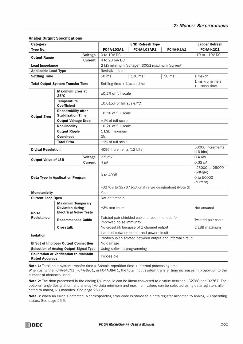
2: MODULE SPECIFICATIONS
Analog Output Specifications
Note 1: Total input system transfer time = Sample repetition time + Internal processing time When using the FC4A-J4CN1, FC4A-J8C1, or FC4A-J8AT1, the total input system transfer time increases in proportion to the number of channels used.
Note 2: The data processed in the analog I/O module can be linear-converted to a value between –32768 and 32767. The optional range designation, and analog I/O data minimum and maximum values can be selected using data registers allo-cated to analog I/O modules. See page 26-12.
Note 3: When an error is detected, a corresponding error code is stored to a data register allocated to analog I/O operating status. See page 26-6.
Category END Refresh Type Ladder RefreshType No. FC4A-L03A1 FC4A-L03AP1 FC4A-K1A1 FC4A-K2C1
Output RangeVoltage 0 to 10V DC –10 to +10V DCCurrent 4 to 20 mA DC
Load Impedance 2 kΩ minimum (voltage), 300Ω maximum (current)Applicable Load Type Resistive loadSettling Time 50 ms 130 ms 50 ms 1 ms/ch
Total Output System Transfer Time Settling time + 1 scan time1 ms × channels + 1 scan time
Output Error
Maximum Error at 25°C
±0.2% of full scale
Temperature Coefficient
±0.015% of full scale/°C
Repeatability after Stabilization Time
±0.5% of full scale
Output Voltage Drop ±1% of full scaleNon-lineality ±0.2% of full scaleOutput Ripple 1 LSB maximumOvershoot 0%Total Error ±1% of full scale
Digital Resolution 4096 increments (12 bits)50000 increments (16 bits)
Output Value of LSBVoltage 2.5 mV 0.4 mVCurrent 4 µA 0.32 µA
Data Type in Application Program0 to 4095
–25000 to 25000 (voltage)0 to 50000 (current)
–32768 to 32767 (optional range designation) (Note 2)Monotonicity YesCurrent Loop Open Not detectable
Noise Resistance
Maximum Temporary Deviation during Electrical Noise Tests
±3% maximum Not assured
Recommended CableTwisted pair shielded cable is recommended for improved noise immunity
Twisted pair cable
Crosstalk No crosstalk because of 1 channel output 2 LSB maximum
IsolationIsolated between output and power circuitPhotocoupler-isolated between output and internal circuit
Effect of Improper Output Connection No damageSelection of Analog Output Signal Type Using software programmingCalibration or Verification to Maintain Rated Accuracy
Impossible
FC5A MICROSMART USER’S MANUAL 2-51

2: MODULE SPECIFICATIONS
Analog I/O Module Terminal Arrangement and Wiring Diagrams
FC4A-L03A1 (Analog I/O Module) — Screw Terminal TypeApplicable Terminal Block: FC4A-PMT11P (supplied with the analog I/O module)
FC4A-L03AP1 (Analog I/O Module) — Screw Terminal TypeApplicable Terminal Block: FC4A-PMT11P (supplied with the analog I/O module)
Terminal No. Channel+
24V DC–
+OUT
–NC
IN0+–
NCIN1+
–
• Connect a fuse appropriate for the applied voltage and current draw, at the position shown in the diagram. This is required when equipment containing the MicroSmart is destined for Europe.
• Do not connect any wiring to unused terminals.• Before turn on the power, make sure that wiring to the analog I/O module is correct. If wiring is
incorrect, the analog I/O module may be damaged.
Fuse+–
24V DC
Analog voltage/current input device
+
–
+
–
+
–
Analog voltage/current output device
Analog voltage/current output device
Terminal No. Channel+
24V DC–
+OUT
–NC A
IN0+ B’– B
NC AIN1+ B’
– BThermocouple
• Connect a fuse appropriate for the applied voltage and current draw, at the position shown in the diagram. This is required when equipment containing the MicroSmart is destined for Europe.
• When connecting a resistance thermometer, connect the three wires to RTD (resistance temper-ature detector) terminals A, B’, and B of input channel IN0 or IN1.
• When connecting a thermocouple, connect the two wires to terminals + and – of input channels IN0 or IN1.
• Do not connect any wiring to unused terminals.• Do not connect the thermocouple to a hazardous voltage (60V DC or 42.4V peak or higher).
Fuse+–
24V DC
Resistance thermometer
+
–
B
+
–AB’
Analog voltage/current input device
2-52 FC5A MICROSMART USER’S MANUAL

2: MODULE SPECIFICATIONS
FC4A-J2A1 (Analog Input Module) — Screw Terminal TypeApplicable Terminal Block: FC4A-PMT11P (supplied with the analog input module)
FC4A-J4CN1 (Analog Input Module) — Screw Terminal TypeApplicable Terminal Block: FC4A-PMT10P (supplied with the analog input module)
Terminal No. Channel+
24V DC–
NC—
NCNC
IN0+–
NCIN1+
–
• Connect a fuse appropriate for the applied voltage and current draw, at the position shown in the diagram. This is required when equipment containing the MicroSmart is destined for Europe.
• Do not connect any wiring to unused terminals.
Fuse+–
24V DC
+
–
+
–
Analog voltage/current output device
Analog voltage/current output device
Terminal No. Channel24V
24V DC0V
NC —CS
IN0+–I–CS
IN1+
–IN1
I–CS
IN2+–I–CS
IN3+–I–
• Connect a fuse appropriate for the applied voltage and current draw, at the position shown in the diagram. This is required when equipment containing the MicroSmart is destined for Europe.
• When connecting a resistance thermometer, connect three wires B, B’, and A to the CS (current sense), +, and – termi-nals of input channels IN0 through IN3, respectively.
• When connecting a thermocouple, connect the + wire to the + terminal and the – wire to the CS and – terminals.• Do not connect the thermocouple to a hazardous voltage (60V DC or 42.4V peak or higher).• Do not connect any wiring to unused terminals.• – terminals of input channels IN0 through IN3 are interconnected.
Fuse+–
24V DC
Analog voltage output device –
+
Resistance thermometer A
BB’
Thermocouple+
–
NC
–
+
NC
NC
Analog current output device
FC5A MICROSMART USER’S MANUAL 2-53

2: MODULE SPECIFICATIONS
FC4A-J8C1 (Analog Input Module) — Screw Terminal TypeApplicable Terminal Block: FC4A-PMT10P (supplied with the analog input module)
FC4A-J8AT1 (Analog Input Module) — Screw Terminal TypeApplicable Terminal Block: FC4A-PMT10P (supplied with the analog input module)
Terminal No. Channel24V
24V DC0V
NC —+
IN0–+
IN1–+
IN2–
+IN3
–+
IN4–+
IN5–+
IN6–+
IN7–
Fuse+–
24V DC
Analog voltage output device –
+
Analog current output device –
+
• Connect a fuse appropriate for the applied voltage and current draw, at the position shown in the diagram. This is required when equipment containing the MicroSmart is destined for Europe.
• Do not connect any wiring to unused terminals.• – terminals of input channels IN0 through IN7 are
interconnected.
Terminal No. Channel24V
24V DC0V
NC —A
IN0BA
IN1BA
IN2B
AIN3
BA
IN4BA
IN5BA
IN6BA
IN7B
Fuse+–
24V DC
NTC Thermistor B
A
PTC Thermistor B
A
• Connect a fuse appropriate for the applied voltage and current draw, at the position shown in the diagram. This is required when equipment containing the MicroSmart is destined for Europe.
• Do not connect any wiring to unused terminals.
2-54 FC5A MICROSMART USER’S MANUAL

2: MODULE SPECIFICATIONS
FC4A-K1A1 (Analog Output Module) — Screw Terminal TypeApplicable Terminal Block: FC4A-PMT11P (supplied with the analog output module)
FC4A-K2C1 (Analog Output Module) — Screw Terminal TypeApplicable Terminal Block: FC4A-PMT10P (supplied with the analog output module)
Terminal No. Channel+
24V DC–
+OUT
–NC
—NCNCNC
—NCNC
• Connect a fuse appropriate for the applied voltage and current draw, at the position shown in the diagram. This is required when equipment containing the MicroSmart is destined for Europe.
• Do not connect any wiring to unused terminals.
Fuse+–
24V DC
+
–Analog voltage/current
input device
Terminal No. Channel24V
24V DC0V
NC —V+
OUT0I+–
V+OUT1I+
–
Fuse+–
24V DC
+
–
Analog voltageinput device
+
–
NC
NCAnalog currentinput device
• Connect a fuse appropriate for the applied voltage and current draw, at the position shown in the diagram. This is required when equipment containing the MicroSmart is destined for Europe.
• Do not connect any wiring to unused terminals.• – terminals of output channels OUT0 and OUT1 are interconnected.
FC5A MICROSMART USER’S MANUAL 2-55
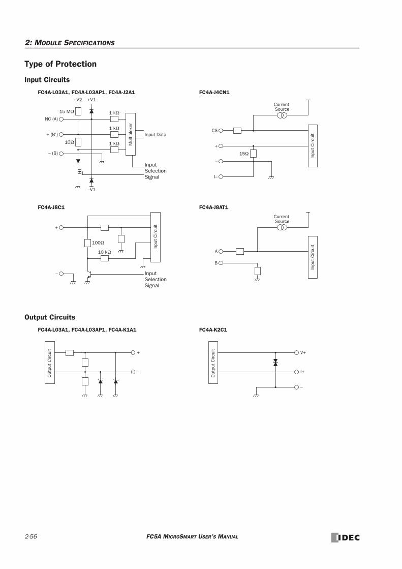
2: MODULE SPECIFICATIONS
Type of Protection
Input Circuits
Output Circuits
1 kΩNC (A)
Mul
tiple
xer
+ (B’)
FC4A-L03A1, FC4A-L03AP1, FC4A-J2A1
– (B)
1 kΩ
1 kΩ
+V2 +V1
–V1
10Ω
Input Data
Input Selection Signal
FC4A-J4CN1
15 MΩ
CS
Inpu
t C
ircui
t
+
–
I–
15Ω
Current Source
+
Inpu
t C
ircui
t
–
FC4A-J8C1
10 kΩ
Input Selection Signal
100Ω
FC4A-J8AT1
A
Inpu
t C
ircui
t
B
Current Source
FC4A-L03A1, FC4A-L03AP1, FC4A-K1A1 FC4A-K2C1
Out
put
Circ
uit
+
–
Out
put
Circ
uit
V+
I+
–
2-56 FC5A MICROSMART USER’S MANUAL

2: MODULE SPECIFICATIONS
Notes for Using the Analog I/O Modules:
• Use separate power supplies for the MicroSmart CPU module and analog I/O modules. Power up the analog I/O modules at least 1 second earlier than the CPU module. This is recommended to ensure correct operation of the analog I/O control.
• Separate the analog I/O lines, particularly resistance thermometer inputs, from motor lines as much as possible to sup-press the influence of noises.
Terminal No. Channel+
24V DC–
+OUT
–NC A
IN0+ B’– B
NC AIN1+ B’
– B
Fuse+–
24V DC
Resistance thermometer B
+
–AB’
Analog voltage/current input device
+
–Analog voltage/current
output device
Separate the analog I/O line from the power line.
FC5A MICROSMART USER’S MANUAL 2-57
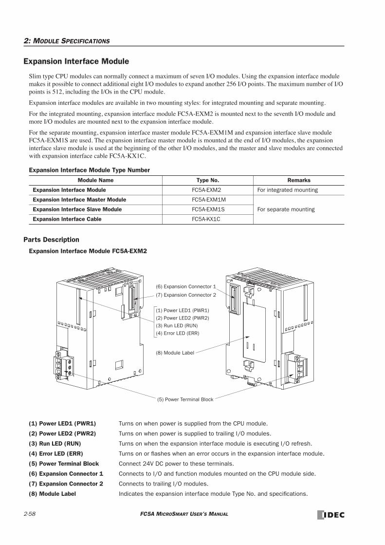
2: MODULE SPECIFICATIONS
Expansion Interface Module
Slim type CPU modules can normally connect a maximum of seven I/O modules. Using the expansion interface module makes it possible to connect additional eight I/O modules to expand another 256 I/O points. The maximum number of I/O points is 512, including the I/Os in the CPU module.
Expansion interface modules are available in two mounting styles: for integrated mounting and separate mounting.
For the integrated mounting, expansion interface module FC5A-EXM2 is mounted next to the seventh I/O module and more I/O modules are mounted next to the expansion interface module.
For the separate mounting, expansion interface master module FC5A-EXM1M and expansion interface slave module FC5A-EXM1S are used. The expansion interface master module is mounted at the end of I/O modules, the expansion interface slave module is used at the beginning of the other I/O modules, and the master and slave modules are connected with expansion interface cable FC5A-KX1C.
Expansion Interface Module Type Number
Parts Description
Expansion Interface Module FC5A-EXM2
(1) Power LED1 (PWR1) Turns on when power is supplied from the CPU module.
(2) Power LED2 (PWR2) Turns on when power is supplied to trailing I/O modules.
(3) Run LED (RUN) Turns on when the expansion interface module is executing I/O refresh.
(4) Error LED (ERR) Turns on or flashes when an error occurs in the expansion interface module.
(5) Power Terminal Block Connect 24V DC power to these terminals.
(6) Expansion Connector 1 Connects to I/O and function modules mounted on the CPU module side.
(7) Expansion Connector 2 Connects to trailing I/O modules.
(8) Module Label Indicates the expansion interface module Type No. and specifications.
Module Name Type No. Remarks
Expansion Interface Module FC5A-EXM2 For integrated mounting
Expansion Interface Master Module FC5A-EXM1M
For separate mountingExpansion Interface Slave Module FC5A-EXM1S
Expansion Interface Cable FC5A-KX1C
(6) Expansion Connector 1
(8) Module Label
(1) Power LED1 (PWR1)
(4) Error LED (ERR)
(2) Power LED2 (PWR2)
(3) Run LED (RUN)
(5) Power Terminal Block
(7) Expansion Connector 2
2-58 FC5A MICROSMART USER’S MANUAL

2: MODULE SPECIFICATIONS
Expansion Interface Master Module FC5A-EXM1M
Expansion Interface Slave Module FC5A-EXM1S
(1) Power LED1 (PWR1) Turns on when power is supplied to the expansion interface module.
(2) Power LED2 (PWR2) Turns on when power is supplied to trailing I/O modules.
(3) Run LED (RUN) Turns on when the expansion interface module is executing I/O refresh.
(4) Error LED (ERR) Turns on or flashes when an error occurs in the expansion interface module.
(5) Expansion Connector 1 Connects to I/O and function modules mounted on the CPU module side.
(6) Expansion Connector 2 Connects to trailing I/O modules.
(7) Expansion Interface Cable Connector Connects the expansion interface cable.
(8) Module Label Indicates the expansion interface module Type No. and specifications.
(9) Power Terminal Block Connect 24V DC power to these terminals.
(5) Expansion Connector 1
(8) Module Label
(1) Power LED1 (PWR1)
(4) Error LED (ERR)
(3) Run LED (RUN)
(7) Expansion Interface Cable Connector
(6) Expansion Connector 2
(9) Power Terminal Block
(7) Expansion Interface Cable Connector
(2) Power LED2 (PWR2)
(8) Module Label
FC5A MICROSMART USER’S MANUAL 2-59

2: MODULE SPECIFICATIONS
General Specifications (Expansion Interface Module)
Note 1: Power consumption by the expansion interface module and eight I/O modules
Note 2: The maximum number of relay outputs that can be turned on simultaneously is 54 points.
Type No.FC5A-EXM2
Expansion Interface Module
FC5A-EXM1MExpansion Interface
Master Module
FC5A-EXM1SExpansion Interface
Slave Module
Rated Power Voltage24V DC (supplied from external power)
—24V DC (supplied from external power)
Allowable Voltage Range20.4 to 26.4V DC (including ripple)
—20.4 to 26.4V DC (including ripple)
Current Draw
Internal power (supplied from CPU module):
50 mA (5V DC) 0 mA (24V DC)
External power:With I/O modules (Note 1)
750 mA (26.4V DC)
Internal power (supplied from CPU module):
90 mA (5V DC) 0 mA (24V DC)
Internal power (supplied from CPU module):
0 mA (5V DC) 0 mA (24V DC)
External power:With I/O modules (Note 1)
750 mA (26.4V DC)Maximum Power Consumption (External Power) (Note 1)
19W (26.4V DC) — 19 (26.4V DC)
Allowable Momentary Power Interruption
10 ms minimum (24V DC)
—10 ms minimum (24V DC)
Applicable CPU Module Slim type CPU modules
I/O Expansion
Between CPU module and expansion interface module:7 I/O modules maximum (6 modules maximum incl. a maximum of 2 AS-Interface master modules)
Beyond the expansion interface module:8 digital I/O modules maximum (AC input modules are not applicable) (Note 2)
I/O Refresh Time See page A-4.Communication through Expansion Interface Cable
— Proprietary protocol
Isolation from Internal Circuit Not isolated Only communication interface part is isolated.Dielectric Strength Between power and terminals: 500V AC, 1 minuteInsulation Resistance Between power and terminals: 10 MΩ minimum (500V DC megger)
Noise ResistanceDC power terminals: 1.0 kV, 50 ns to 1 µs Expansion interface cable (coupling clamp): 1.5 kV, 50 ns to 1 µs
Inrush Current 50A maximum (24V DC)Grounding Wire UL1015 AWG22, UL1007 AWG18Power Supply Wire UL1015 AWG22, UL1007 AWG18EMC Compliant Cable Length — 1m (FC5A-KX1C)
Power Supply Connector
Connector on Mother Board
MSTB2.5/3-GF-5.08BK (Phoenix Contact)
—MKDSN1.5/3-5.08-BK (Phoenix Contact)
Connector Insertion/ Removal Durability
100 times minimum — —
Expansion Cable Connector
Connector on Mother Board
—FCN-365P024-AU (Fujitsu Component)
FCN-365P024-AU (Fujitsu Component)
Connector Insertion/ Removal Durability
— 100 times minimum 100 times minimum
Effect of Improper Power Supply Connection
Reverse polarity: No operation, no damage Improper voltage: Permanent damage may be caused Improper lead connection: Permanent damage may be caused
Effect of Improper Expansion Cable Connection
—
Reverse polarity: Permanent damage may be caused Improper voltage Permanent damage may be caused Improper lead connection: Permanent damage may be caused
Weight 140g 70g 135g
2-60 FC5A MICROSMART USER’S MANUAL

2: MODULE SPECIFICATIONS
Error LEDThe ERR LED on expansion interface modules flashes and turns on depending on the error condition.
Note: When an AC input module is mounted to the right of the expansion interface module, the ERR LED does not turn on.
Special Data Register for Expansion Interface ModuleSlim type CPU modules have a special data register for the expansion interface module. Special data register D8252 stores the refresh time (in units of 100 µs) of additional expansion I/O modules mounted to the right of the expansion interface module.
Error LED Description
Turns ONWhen the CPU module has an error.When the scan time exceeds 1000 ms.(Do not set the constant scan time of special data register D8022 to longer than 1000 ms.)
Flashes (500ms period)
When the expansion interface module or the expansion interface slave module is not powered by the external power supply.
Flashes (1000ms period)
When an initialization error occurred in an I/O module connected to the right of the expansion inter-face module.When more than eight I/O modules are mounted to the right of the expansion interface module.When any module other than digital I/O modules is mounted to the right of the expansion interface module.
DR No. Data Register Function DR Value Updated R/W
D8252 Expansion interface module I/O refresh time (×100 µs) Every scan R
FC5A MICROSMART USER’S MANUAL 2-61

2: MODULE SPECIFICATIONS
Expansion Interface Module Terminal Arrangement
FC5A-EXM2 (Expansion Interface Module)Applicable Terminal Block: MSTB2.5/3-GF-5.08BK (supplied with the expansion interface module)
FC5A-EXM1M (Expansion Interface Master Module) FC5A-EXM1S (Expansion Interface Slave Module)
EX
PWR2RUNERR
PWR1
24V D
C+
–
• For power wiring precautions, see page 2-63.
EX
RUNERR
PWR1
EX
PWR2
• For power wiring precautions, see page 2-63.Applicable Cable: FC5A-KX1C
2-62 FC5A MICROSMART USER’S MANUAL

2: MODULE SPECIFICATIONS
Expansion Interface Module System Setup
FC5A-EXM2 (Expansion Interface Module)
FC5A-EXM1M and FC5A-EXM1S (Expansion Interface Master and Slave Modules)
Notes:• Use one power supply to power the CPU module and the expansion interface module or expansion interface slave module.
• When using a separate power supply, power up the expansion interface module or expansion interface slave module first, followed by the CPU module, otherwise the CPU module causes an error and cannot start and stop operation.
• Use the optional expansion interface cable FC5A-KX1C for connection between the expansion interface master and slave modules.
• If the expansion interface cable is disconnected during operation, the I/O modules connected to the expansion interface slave module are reset and all I/O points are turned off automatically. Then, turn off the power to the CPU module and the expansion interface slave module, connect the cable, and turn on the power again.
• Only one expansion interface module can be used with the CPU module.
• AC input module, analog I/O modules, and AS-Interface master module cannot be connected to the right of the expansion interface module. When AC input module is connected, the ERR LED on the CPU module does not turn on. Make sure that AC input module is not connected to the right of the expansion interface module.
Power Supply Wiring Example
Slim Type CPU Module FC5A-EXM2
Slim Type CPU Module FC5A-EXM1M
FC5A-EXM1S
FC5A-KX1C (Expansion Inter face Cable)
(1m)
24V DC
+ –
+–
+ –
CPU ModuleSlim Type
Expansion Interface ModuleExpansion Interface Slave Module
FC5A MICROSMART USER’S MANUAL 2-63

2: MODULE SPECIFICATIONS
AS-Interface Master Module
The AS-Interface master module can be used with the all-in-one 24-I/O type and any slim type CPU modules to communi-cate digital data with slaves, such as sensor, actuator, and remote I/O data.
One or two AS-Interface master modules can be used with one CPU module. The AS-Interface master module can connect a maximum of 62 digital I/O slaves. A maximum of seven analog I/O slaves can also be connected to the AS-Interface master module (compliant with AS-Interface ver. 2.1 and analog slave profile 7.3).
AS-Interface Master Module Type Number
Parts Description
(1) LED Indicators Status LEDs: Indicate the AS-Interface bus status. I/O LEDs: Indicate the I/O status of the slave specified by the address LEDs. Address LEDs: Indicate slave addresses.
(2) Pushbuttons Used to select slave addresses, change modes, and store configuration.
(3) AS-Interface Cable Terminal Block
Connects the AS-Interface cable. One terminal block is supplied with the AS-Interface master module. When ordering separately, specify Type No. FC4A-PMT3P and quantity (package quantity: 2).
(4) AS-Interface Cable Connector
Installs the AS-Interface cable terminal block.
(5) Unlatch Button Used to unlatch the AS-Interface master module from the CPU or I/O module.
(6) Expansion Connector Connects to the CPU and other I/O modules.
(7) Module Label Indicates the AS-Interface master module Type No. and specifications.
Module Name Type No.
AS-Interface Master Module FC4A-AS62M
(6) Expansion Connector
(7) Module Label
(1) LED Indicators
(4) AS-Interface Cable Connector
(2) PushbuttonsPB1PB2
(5) Unlatch Button
(5) Unlatch Button
(3) AS-Interface Cable Terminal Block (supplied with the AS-Interface master module)
2-64 FC5A MICROSMART USER’S MANUAL
2: MODULE SPECIFICATIONS
General Specifications (AS-Interface Module)
Communication Specifications (AS-Interface Module)
Note: When using two AS-Interface modules, these quantities are doubled.
Operating Temperature 0 to 55°C (operating ambient temperature, no freezing)
Storage Temperature –25 to +70°C (no freezing)
Relative Humidity Level RH1, 30 to 95% (non-condensing)
Pollution Degree 2 (IEC 60664)
Degree of Protection IP20
Corrosion Immunity Free from corrosive gases
AltitudeOperation: 0 to 2,000m (0 to 6,565 feet)Transport: 0 to 3,000m (0 to 9,840 feet)
Vibration Resistance
When mounted on a DIN rail:10 to 57 Hz amplitude 0.075 mm, 57 to 150 Hz acceleration 9.8 m/s2
2 hours per axis on each of three mutually perpendicular axes
When mounted on a panel surface:2 to 25 Hz amplitude 1.6 mm, 25 to 100 Hz acceleration 39.2 m/s2
90 minutes per axis on each of three mutually perpendicular axes
Shock Resistance147 m/s2, 11 ms duration, 3 shocks per axis, on three mutually perpendic-ular axes (IEC 61131)
External Power Supply AS-Interface power supply, 29.5 to 31.6V DC
AS-Interface Current Draw65 mA (normal operation)110 mA maximum
Effect of Improper Input Connection No damage
Connector on Mother Board MSTB2.5/3-GF-5.08BK (Phoenix Contact)
Connector Insertion/Removal Durability 100 times minimum
Internal Current Draw80 mA (5V DC) 0 mA (24V DC)
AS-Interface Master Module Power Consumption
540 mW
Weight 85g
Maximum Bus Cycle
When 1 through 19 slaves are connected: 3 ms When 20 through 62 slaves are connected: 0.156 × (1 + N) ms where N is the number of active slaves
5 ms maximum when 31 standard or A/B slaves are connected10 ms maximum when 62 A/B slaves are connected
Maximum Slaves (Note)
Standard slaves: 31A/B slaves: 62
When using a mix of standard slaves and A/B slaves together, the standard slaves can only use addresses 1(A) through 31(A). Also, when a standard slave takes a certain address, the B address of the same number cannot be used for A/B slaves.
Maximum I/O Points (Note)Standard slaves: 248 total (124 inputs + 124 outputs) A/B slaves: 434 total (248 inputs + 186 outputs)
Maximum Cable LengthAS-Interface cable2-wire flat cable
When using no repeater or extender: 100m When using a total of 2 repeaters or extenders: 300m
Single wires 200 mm
Rated Bus Voltage 30V DC
FC5A MICROSMART USER’S MANUAL 2-65

2: MODULE SPECIFICATIONS
HMI ModuleThe optional HMI module can mount on any all-in-one type CPU module, and also on the HMI base module mounted next to any slim type CPU module. The HMI module makes it possible to manipulate the RAM data in the CPU module with-out using the Online menu options in WindLDR. For details about operating the HMI module, see page 5-50. For installing and removing the HMI module, see pages 3-3 and 3-4.
HMI Module Type Number
Parts Description
(1) Display Screen The liquid crystal display shows menus, operands, and data.
(2) ESC Button Cancels the current operation, and returns to the immediately preceding operation.
(3) Button Scrolls up the menu, or increments the selected operand number or value.
(4) Button Scrolls down the menu, or decrements the selected operand number or value.
(5) OK Button Goes into each control screen, or enters the current operation.
(6) HMI Connector Connects to the all-in-one CPU module or HMI base module.
HMI Module Specifications
Module Name Type No.
HMI Module FC4A-PH1
Type No. FC4A-PH1
Power Voltage 5V DC (supplied from the CPU module)
Internal Current Draw 200 mA DC
Weight 20g
(1) Display Screen
(2) ESC Button (6) HMI Connector(3) Button (4) Button (5) OK Button
Caution • Turn off the power to the MicroSmart before installing or removing the HMI module to prevent electrical shocks and damage to the HMI module.
• Do not touch the connector pins with hand, otherwise contact characteristics of the connector may be impaired.
2-66 FC5A MICROSMART USER’S MANUAL

2: MODULE SPECIFICATIONS
HMI Base ModuleThe HMI base module is used to install the HMI module when using the slim type CPU module. The HMI base module also has a port 2 connector to attach an optional RS232C or RS485 communication adapter.
When using the all-in-one type CPU module, the HMI base module is not needed to install the HMI module.
HMI Base Module Type Number
Parts Description
(1) HMI Connector For installing the HMI module.
(2) Hinged Lid Open the lid to gain access to the port 2 connector.
(3) Port 2 Connector For installing an optional RS232C or RS485 communication adapter.
(4) Communication Connector Connects to the slim type CPU module.
Module Name Type No.
HMI Base Module FC4A-HPH1
(1) HMI Connector
(2) Hinged Lid
(4) Communication Connector
(3) Port 2 Connector
FC5A MICROSMART USER’S MANUAL 2-67

2: MODULE SPECIFICATIONS
Communication Adapters and Communication ModulesAll MicroSmart CPU modules have communication port 1 for RS232C communication. In addition, all-in-one type CPU modules have a port 2 connector. An optional communication adapter can be installed on the port 2 connector for RS232C or RS485 communication.
A communication module can be attached to any slim type CPU module to use port 2 for additional RS232C or RS485 communication. When the HMI base module is attached to a slim type CPU module, a communication adapter can be installed to the port 2 connector on the HMI base module.
When using the RS232C communication adapter or communication module for port 2, maintenance communication, user communication, and modem communication are made possible. With the RS485 communication adapter or communica-tion module installed, maintenance communication, user communication, data link communication, and Modbus master and slave communication can be used on port 2.
Communication Adapter and Communication Module Type Numbers
Communication Adapter and Communication Module Specifications
Note 1: 1:1 Modbus communication only
Note 2: For special cables, see page A-7.
Note 3: Recommended cable for RS485: Twisted-pair shielded cable with a minimum core wire of 0.3 mm2. Conductor resistance 85 Ω/km maximum, shield resistance 20 Ω/km maximum.
The proper tightening torque of the terminal screws on the RS485 communication adapter and RS485 communication mod-ule is 0.22 to 0.25 N·m. For tightening the screws, use screwdriver SZS 0,4 x 2,5 (Phoenix Contact).
Name Termination Type No.
RS232C Communication Adapter Mini DIN connector FC4A-PC1
RS485 Communication AdapterMini DIN connector FC4A-PC2
Screw Terminal Block FC4A-PC3
RS232C Communication Module Mini DIN connector FC4A-HPC1
RS485 Communication ModuleMini DIN connector FC4A-HPC2
Screw Terminal Block FC4A-HPC3
Type No.FC4A-PC1
FC4A-HPC1FC4A-PC2
FC4A-HPC2FC4A-PC3
FC4A-HPC3
Standards EIA RS232C EIA RS485 EIA RS485
Communication Method Asynchronous Asynchronous Asynchronous
Port No. 2 2 2
Maximum Connectable Quantity 1 1 1
Maximum Baud Rate 57,600 bps 57,600 bps 57,600 bps
Maintenance Communication(Computer Link)
Possible Possible Possible
User Communication Possible — Possible
Modem Communication Possible — —
Data Link Communication — —Possible (31 slaves max.)
Modbus Communication Possible (Note 1) — Possible
Maximum Cable LengthSpecial cable (Note 2)
Special cable (Note 2)
200m (Note 3)
Isolation between Internal Circuit and Communication Port
Not isolated Not isolated Not isolated
2-68 FC5A MICROSMART USER’S MANUAL

2: MODULE SPECIFICATIONS
Parts Description
(1) Port 2 RS232C or RS485 communication port 2.(2) Connector Connects to the port 2 connector on the all-in-one type CPU module or HMI base module.
(1) Communication Connector Connects to the slim type CPU module.(2) Port 2 RS232C or RS485 communication port 2.(3) Hinged Lid Open the lid to gain access to port 2.
(1) Expansion Connector Connects to the CPU and other I/O modules.(2) Module Label Indicates the module Type No. and specifications.(3) Power LED Turns on when power is supplied to the module.(4) Terminal No. Indicates terminal numbers.(5) Cable Terminal Removable terminal blocks
(1) Port 2
(2) Connector
RS232C Communication Adapter (Mini DIN) RS485 Communication Adapter (Mini DIN)
RS485 Communication Adapter (Screw Terminal)
(1) Port 2
(2) Connector
(2) Port 2
RS232C Communication Module (Mini DIN) RS485 Communication Module (Mini DIN)
RS485 Communication Module (Screw Terminal)
(1) Communication Connector
(3) Hinged Lid
(2) Port 2
(1) Communication Connector
(3) Hinged Lid
Expansion RS232C Communication Module (Screw Terminal)
(1) Expansion Connector
(2) Module Label
(3) Power LED (PWR)
(4) Terminal No.
(5) Cable Terminal
FC5A MICROSMART USER’S MANUAL 2-69

2: MODULE SPECIFICATIONS
Installing the Communication Adapter and Communication Module
Communication AdapterTo install the communication adapter on the all-in-one type CPU module, open the hinged lid and remove the dummy car-tridge. Push the communication adapter into the port 2 connector from the front until it bottoms and is secured by the latches. Similarly, when installing the communication adapter on the HMI base module, open the hinged lid, and push the communication adapter into the port 2 connector from the front until it bottoms and is secured by the latches.
After installing the communication adapter on an all-in-one type CPU module, view the communication adapter through the dummy cartridge opening, and check to see that the PC board of the communication adapter is in a lower level than the top of the terminal block.
Caution • Before installing the communication adapter or communication module, turn off the power to the MicroSmart CPU module. Otherwise, the communication adapter or CPU module may be dam-aged, or the MicroSmart may not operate correctly.
Communication Adapter
Hinged Lid
Dummy CartridgeAfter installing the communication adapter, attach the dummy cartridge again.
Port 2 Connector
Communication Adapter
Port 2 Connector
Hinged Lid
Communication Adapter PC Board
Terminal Block
2-70 FC5A MICROSMART USER’S MANUAL

2: MODULE SPECIFICATIONS
Communication ModuleWhen installing a communication module on the slim type CPU module, remove the communication connector cover from the slim type CPU module. See page 3-6.
Place the communication module and CPU module side by side. Put the communication connectors together for easy alignment.
With the communication connectors aligned correctly and the blue unlatch button in the down position, press the communica-tion module and CPU module together until the latches click to attach the modules together firmly. If the unlatch button is in the up position, push down the button to engage the latches.
Removing the Communication Adapter and Communication Module
Communication AdapterTo remove the communication adapter from the all-in-one type CPU module, first remove the dummy cartridge. While pushing up the communication adapter PC board with a finger through the dummy cartridge opening, disengage the latches from the communication adapter using a flat screwdriver. Pull out the communication adapter from the port 2 connector. When removing the communication adapter from the HMI module, take similar steps.
Communication ModuleIf the modules are mounted on a DIN rail, first remove the modules from the DIN rail as described on page 3-7.
Push up the blue unlatch button to disengage the latches, and pull the modules apart as shown on the right.
Unlatch Button Communication Connector Cover
Communication Module Slim Type CPU Module
Caution • Before removing the communication adapter or communication module, turn off the power to the MicroSmart CPU module. Otherwise, the communication adapter or CPU module may be dam-aged, or the MicroSmart may not operate correctly.
Unlatch Button
FC5A MICROSMART USER’S MANUAL 2-71
2: MODULE SPECIFICATIONS
Memory CartridgeA user program can be stored on an optional memory cartridge installed on a MicroSmart CPU module from a computer running WindLDR, and the memory cartridge can be installed on another MicroSmart CPU module of the same type. Using a memory cartridge, the CPU module can exchange user programs where a computer cannot be used.
This feature is available on all models of CPU modules.
Memory Cartridge Type Number
User Program Execution PriorityDepending whether a memory cartridge is installed on the MicroSmart CPU module or not, a user program stored on the memory cartridge or on the CPU module EEPROM is executed, respectively.
Memory Cartridge Specifications
Note: The optional clock cartridge (FC4A-PT1) and the memory cartridge cannot be used together on the all-in-one type CPU module. The clock cartridge and the memory cartridge can be used together on the slim type CPU module.
User Program CompatibilityThe CPU module can execute only user programs created for the same CPU module type. When installing a memory car-tridge, make sure that the user program stored on the memory cartridge matches the CPU module type. If the user program is not for the same CPU module type, a user program syntax error occurs and the CPU module cannot run the user pro-gram.
Module Name Type No.
32KB Memory Cartridge FC4A-PM32
64KB Memory Cartridge FC4A-PM64
Memory Cartridge User Program Execution Priority
Installed on the CPU Module
The user program stored on the memory cartridge is executed.When the memory cartridge does not store a user program, the user program on the CPU module EEPROM is executed.When a memory cartridge is installed on the CPU module, the user program can be downloaded from the memory cartridge to the CPU module by designat-ing in WindLDR Function Area Settings.
Not installed on the CPU Module The user program stored on the EEPROM in the CPU module is executed.
Type No. FC4A-PM32 FC4A-PM64
Memory Type EEPROM
Accessible Memory Capacity 32 KB 64 KB
Hardware for Storing Data CPU module
Software for Storing Data WindLDR
Quantity of Stored Programs One user program can be stored on one memory cartridge.
• Compatibility of User Program with CPU Modules When a memory cartridge contains a user program for higher functionality, do not install the mem-ory cartridge into CPU modules with lower functionality, otherwise the user program is not exe-cuted correctly. Make sure that the user program in the memory cartridge is compatible with the CPU module.
Caution
2-72 FC5A MICROSMART USER’S MANUAL

2: MODULE SPECIFICATIONS
Downloading and Uploading User Program to and from Memory Cartridge Using WindLDRWhen a memory cartridge is installed on the CPU module, a user program is downloaded to and uploaded from the mem-ory cartridge using WindLDR on a computer. When a memory cartridge is not installed on the CPU module, a user program is downloaded to and uploaded from the CPU module. For the procedures to download a user program from WindLDR on a computer, see page 4-10.
With a memory cartridge installed on a CPU module, if the user program stored on the memory cartridge does not match the CPU module type, downloading is possible, but uploading is not possible. To upload a user program, make sure that the existing user program stored on the memory cartridge matches the CPU module type. Downloading is always possible to new blank memory cartridges installed on any type of CPU modules.
Downloading User Program from Memory Cartridge to the CPU ModuleUsing WindLDR settings, the user program stored on the memory cartridge can be downloaded to the CPU module.
Programming WindLDR
1. From the WindLDR menu bar, select Configure > Function Area Settings. The Function Area Settings dialog box appears.
2. Select the Others tab.
3. Under Memory Cartridge Setting, click the check box to the left of Download the user program from a memory cartridge when installed on a CPU module.
Checked: The user program is downloaded from the memory cartridge to the CPU module.
Unchecked: The user program is not downloaded from the memory cartridge to the CPU module.
With the user program in the CPU module is write-protected or read/write-protected, the user program can be downloaded only when the password in the memory cartridge matches the password in the CPU module. For user program protection password, see page 5-38.
FC5A MICROSMART USER’S MANUAL 2-73

2: MODULE SPECIFICATIONS
Installing and Removing the Memory Cartridge
All-in-One Type CPU ModuleThe cartridge connector is normally closed with a dummy cartridge. To install the memory cartridge, open the terminal cover and remove the dummy car-tridge from the CPU module. Make sure of correct orientation of the memory cartridge. Insert the mem-ory cartridge into the cartridge connector until it bot-toms. Do not insert the memory cartridge diagonally, otherwise the terminal pins will be deformed.
After installing the memory cartridge, close the ter-minal cover.
To remove the memory cartridge, hold both edges of the memory cartridge and pull it out.
Slim Type CPU ModuleCartridge connectors 1 and 2 are normally closed with a dummy cartridge. To install the memory car-tridge, open the hinged lid and remove the dummy cartridge from the CPU module. Make sure of correct orientation of the memory cartridge, and insert the memory cartridge into cartridge connector 1 or 2 until it bottoms. After installing the memory car-tridge, close the hinged lid.
Only one memory cartridge can be installed to either cartridge connector 1 or 2 on the slim type CPU module. A memory cartridge and a clock cartridge can be installed at the same time.
To remove the memory cartridge, hold both edges of the memory cartridge and pull it out.
Caution • Before installing or removing the memory cartridge, turn off the power to the MicroSmart CPU module. Otherwise, the memory cartridge or CPU module may be damaged, or the MicroSmart may not operate correctly.
• Do not touch the connector pins with hand, otherwise electrostatic discharge may damage the internal elements.
Terminal Cover
CartridgeConnector
Memory CartridgeFC4A-PM32
Hinged Lid
Cartridge Connector 1
Memory CartridgeFC4A-PM32
Cartridge Connector 2
2-74 FC5A MICROSMART USER’S MANUAL

2: MODULE SPECIFICATIONS
Clock CartridgeWith the optional clock cartridge installed on any type of MicroSmart CPU modules, the MicroSmart can be used for time-scheduled control such as illumination and air conditioners. For setting the calendar/clock, see page 15-6.
Clock Cartridge Type Number
Clock Cartridge Specifications
The optional memory cartridge (FC4A-PM32) and the clock cartridge cannot be used together on the all-in-one type CPU module. The memory cartridge and the clock cartridge can be used together on the slim type CPU module.
Installing and Removing the Clock Cartridge
All-in-One Type CPU ModuleThe cartridge connector is normally closed with a dummy cartridge. To install the clock cartridge, open the terminal cover and remove the dummy cartridge from the CPU module. Make sure of correct orienta-tion of the clock cartridge. Insert the clock cartridge into the cartridge connector until it bottoms. Do not insert the clock cartridge diagonally, otherwise the terminal pins will be deformed. After installing the clock cartridge, close the terminal cover.
To remove the clock cartridge, hold both edges of the clock cartridge and pull it out.
Slim Type CPU ModuleTo install the clock cartridge, open the hinged lid and remove the dummy cartridge from the CPU module. Make sure of correct orientation of the clock car-tridge, and insert the clock cartridge into cartridge connector 1 or 2 until it bottoms. After installing the clock cartridge, close the hinged lid.
Only one clock cartridge can be installed to either cartridge connector 1 or 2 on the slim type CPU module. A clock cartridge and a memory cartridge can be installed at the same time.
To remove the clock cartridge, hold both edges of the clock cartridge and pull it out.
Module Name Type No.
Clock Cartridge FC4A-PT1
Accuracy ±30 sec/month (typical) at 25°C
Backup Duration Approx. 30 days (typical) at 25°C after backup battery fully charged
Battery Lithium secondary battery
Charging Time Approx. 10 hours for charging from 0% to 90% of full charge
Battery Life Approx. 100 recharge cycles after discharging down to 10% of full charge
Replaceability Impossible to replace battery
Caution • Before installing or removing the clock cartridge, turn off the power to the MicroSmart CPU module. Otherwise, the clock cartridge or CPU module may be damaged, or the MicroSmart may not operate correctly.
• After installing the clock cartridge, set the calendar/clock using WindLDR. If the calendar/clock is set before installing the clock cartridge, clock IC error occurs, turning on the ERR LED.
Terminal Cover
CartridgeConnector
Clock CartridgeFC4A-PT1
Hinged Lid
Cartridge Connector 1
Clock CartridgeFC4A-PT1
Cartridge Connector 2
FC5A MICROSMART USER’S MANUAL 2-75

2: MODULE SPECIFICATIONS
DimensionsAll MicroSmart modules have the same profile for consistent mounting on a DIN rail.
CPU Modules
FC5A-C10R2, FC5A-C10R2C, FC5A-C16R2, FC5A-C16R2C
FC5A-C24R2, FC5A-C24R2C
80.0
90.0
4.5*
70.0
*8.5 mm when the clamp is pulled out.
*8.5 mm when the clamp is pulled out.
95.0 70.0
90.0
4.5*
All dimensions in mm.
2-76 FC5A MICROSMART USER’S MANUAL

2: MODULE SPECIFICATIONS
FC5A-D16RK1, FC5A-D16RS1
FC5A-D32K3, FC5A-D32S3
47.5 14.6 70.0
90.0
4.5
*
*8.5 mm when the clamp is pulled out.
47.5 11.3 70.0
90.0
4.5
*
*8.5 mm when the clamp is pulled out.All dimensions in mm.
FC5A MICROSMART USER’S MANUAL 2-77

2: MODULE SPECIFICATIONS
I/O Modules
FC4A-N08B1, FC4A-N08A11, FC4A-R081, FC4A-T08K1, FC4A-T08S1, FC4A-M08BR1, FC4A-L03A1, FC4A-L03AP1, FC4A-J2A1, FC4A-K1A1, FC4A-K2C1
FC4A-N16B1, FC4A-R161, FC4A-J4CN1, FC4A-J8C1, FC4A-J8AT1
FC4A-M24BR2
23.5 14.6 70.0
90.0
4.5
*
3.8
*8.5 mm when the clamp is pulled out.
23.5 14.6 70.0
90.0
4.5
*
3.8
*8.5 mm when the clamp is pulled out.
All dimensions in mm.
39.1 1.0 70.0
90
.04
.5*
3.8
*8.5 mm when the clamp is pulled out.
2-78 FC5A MICROSMART USER’S MANUAL

2: MODULE SPECIFICATIONS
FC4A-N16B3, FC4A-T16K3, FC4A-T16S3
FC4A-N32B3, FC4A-T32K3, FC4A-T32S3
17.6 11.3 70.0
90.0
4.5
*
3.8
*8.5 mm when the clamp is pulled out.
29.7 11.3 70.0
90.0
4.5
*
3.8
*8.5 mm when the clamp is pulled out.
All dimensions in mm.
FC5A MICROSMART USER’S MANUAL 2-79

2: MODULE SPECIFICATIONS
Expansion Interface Module FC5A-EXM2
Expansion Interface Master Module FC5A-EXM1M
Expansion Interface Slave Module FC5A-EXM1S
39.1 9.4 70.0
90.0
4.5
*
3.8
*8.5 mm when the clamp is pulled out.
*8.5 mm when the clamp is pulled ou
17.6
4.5
*
3.8 60.0 70.0
*8.5 mm when the clamp is pulled out.
35.4
90
4.5
*
60.0 70.0
All dimensions in mm.
2-80 FC5A MICROSMART USER’S MANUAL

2: MODULE SPECIFICATIONS
AS-Interface Module FC4A-AS62M
HMI Module FC4A-PH1
HMI Base Module FC4A-HPH1
10
17.7
37.5
23.5
90.0
4.5
*
3.8 9.4 70.0
*8.5 mm when the clamp is pulled out.
35.0
42.0
38.0 13.9 71.0
90.0
4.5
*
*8.5 mm when the clamp is pulled out.
All dimensions in mm.
FC5A MICROSMART USER’S MANUAL 2-81

2: MODULE SPECIFICATIONS
Communication Modules
FC4A-HPC1, FC4A-HPC2, FC4A-HPC3
Example: The following figure illustrates a system setup consisting of the all-in-one 24-I/O type CPU module, an 8-point relay out-put module, and a 16-point DC input module mounted on a 35-mm-wide DIN rail using BNL6P mounting clips.
22.5 13.9 70.0
90.0
4.5
*
*8.5 mm when the clamp is pulled out.
All dimensions in mm.
*8.5 mm when the clamp is pulled out.
95.09.0
35.0
45.0
23.5 23.5 9.0
4.5*
90.0
BNL6P Mounting ClipDIN Rail
2-82 FC5A MICROSMART USER’S MANUAL
3: INSTALLATION AND WIRING
IntroductionThis chapter describes the methods and precautions for installing and wiring MicroSmart modules.
Before starting installation and wiring, be sure to read “Safety Precautions” in the beginning of this manual and under-stand precautions described under Warning and Caution.
Installation LocationThe MicroSmart must be installed correctly for optimum perfor-mance.
The MicroSmart is designed for installation in a cabinet. Do not install the MicroSmart outside a cabinet.
The environment for using the MicroSmart is “Pollution degree 2.” Use the MicroSmart in environments of pollution degree 2 (accord-ing to IEC 60664-1).
Make sure that the operating temperature does not drop below 0°C or exceed 55°C. If the temperature does exceed 55°C, use a fan or cooler.
Mount the MicroSmart on a vertical plane as shown at right.
To eliminate excessive temperature build-up, provide ample venti-lation. Do not install the MicroSmart near, and especially above, any device which generates considerable heat, such as a heater, transformer, or large-capacity resistor. The relative humidity should be above 30% and below 95%.
The MicroSmart should not be exposed to excessive dust, dirt, salt, direct sunlight, vibrations, or shocks. Do not use the MicroSmart in an area where corrosive chemicals or flammable gases are present. The modules should not be exposed to chemical, oil, or water splashes.
• Turn off the power to the MicroSmart before starting installation, removal, wiring, maintenance, and inspection of the MicroSmart. Failure to turn power off may cause electrical shocks or fire haz-ard.
• Emergency stop and interlocking circuits must be configured outside the MicroSmart. If such a cir-cuit is configured inside the MicroSmart, failure of the MicroSmart may cause disorder of the con-trol system, damage, or accidents.
• Special expertise is required to install, wire, program, and operate the MicroSmart. People without such expertise must not use the MicroSmart.
• Prevent metal fragments and pieces of wire from dropping inside the MicroSmart housing. Put a cover on the MicroSmart modules during installation and wiring. Ingress of such fragments and chips may cause fire hazard, damage, or malfunction.
• Do not touch the connector pins with hand, otherwise electrostatic discharge may damage the inter-nal elements.
• Keep the MicroSmart wiring away from motor lines.
Warning
Caution
Mounting ClipBNL6P
All-in-One Type
Slim Type
Mounting ClipBNL6P
FC5A MICROSMART USER’S MANUAL 3-1

3: INSTALLATION AND WIRING
Assembling Modules
The following example demonstrates the procedure for assembling the all-in-one 24-I/O type CPU module and an I/O module together. When assembling slim type CPU modules, take the same procedure.
1. When assembling an input or output module, remove the expansion connector seal from the 24-I/O type CPU module.
2. Place the CPU module and I/O module side by side. Put the expansion connectors together for easy alignment.
3. With the expansion connectors aligned correctly and the blue unlatch button in the down position, press the CPU module and I/O module together until the latches click to attach the modules together firmly. If the unlatch button is in the up position, push down the button to engage the latches.
Disassembling Modules
1. If the modules are mounted on a DIN rail, first remove the modules from the DIN rail as described on page 3-7.
2. Push up the blue unlatch button to disengage the latches, and pull the modules apart as shown. When dis-assembling slim type CPU modules, take the same proce-dure.
Caution • Assemble MicroSmart modules together before mounting the modules onto a DIN rail. Attempt to assemble modules on a DIN rail may cause damage to the modules.
• Turn off the power to the MicroSmart before assembling the modules. Failure to turn power off may cause electrical shocks.
Unlatch Button
Caution • Remove the MicroSmart modules from the DIN rail before disassembling the modules. Attempt to disassemble modules on a DIN rail may cause damage to the modules.
• Turn off the power to the MicroSmart before disassembling the modules. Failure to turn power off may cause electrical shocks.
Unlatch Button
3-2 FC5A MICROSMART USER’S MANUAL

3: INSTALLATION AND WIRING
Installing the HMI Module
The optional HMI module (FC4A-PH1) can mount on any all-in-one type CPU module, and also on the HMI base module mounted next to any slim type CPU module. For specifications of the HMI module, see page 2-66. For details about oper-ating the HMI module, see page 5-50.
All-in-One Type
1. Remove the HMI connector cover from the CPU module. Locate the HMI connector inside the CPU module.
2. Push the HMI module into the HMI module connector in the CPU module until the latch clicks.
Slim Type
1. When using the HMI module with the slim type CPU mod-ule, prepare the optional HMI base module (FC4A-HPH1). See page 2-67.
2. Locate the HMI connector inside the HMI base module. Push the HMI module into the HMI connector in the HMI base module until the latch clicks.
3. Remove the communication connector cover from the slim type CPU module. See page 3-6.
4. Place the HMI base module and CPU module side by side. With the communication connectors aligned correctly and the blue unlatch button in the down position, press the HMI base module and CPU module together until the latches click to attach the modules together firmly. If the unlatch button is in the up position, push down the button to engage the latches.
Caution • Turn off the power to the MicroSmart before installing or removing the HMI module to prevent electrical shocks.
• Do not touch the connector pins with hand, otherwise electrostatic discharge may damage the internal elements.
HMI Module
HMI Connector
Unlatch Button Communication Connector Cover
Slim Type CPU Module
HMI Base Module
HMI Module
FC5A MICROSMART USER’S MANUAL 3-3

3: INSTALLATION AND WIRING
Removing the HMI Module
This section describes the procedures for removing the HMI module from the optional HMI base module mounted next to any slim type CPU module.
1. Insert a thin flat screwdriver (ø3.0 mm maximum) between the gap on top of the HMI module until the tip of the screwdriver bottoms.
2. While turning the screwdriver in the direction as shown, disen-gage the latch on the HMI module and pull out the HMI module.
3. Remove the HMI module from the HMI base module.
Caution • Turn off the power to the MicroSmart before installing or removing the HMI module to prevent electrical shocks.
• Do not touch the connector pins with hand, otherwise electrostatic discharge may damage the internal elements.
Latch
3-4 FC5A MICROSMART USER’S MANUAL

3: INSTALLATION AND WIRING
Removing the Terminal Blocks
This section describes the procedures for removing the terminal blocks from slim type CPU modules FC5A-D16RK1 and FC5A-D16RS1.
1. Before removing the terminal blocks, disconnect all wires from the terminal blocks.
Remove the shorter terminal block on the left first, then remove the longer one on the right.
2. When removing the longer terminal block, hold the center of the terminal block, and pull it out straight.
3. Do not pull one end of the longer terminal block, otherwise the terminal block may be damaged.
Caution • Turn off the power to the MicroSmart before installing or removing the terminal blocks to pre-vent electrical shocks.
• Use the correct procedures to remove the terminal blocks, otherwise the terminal blocks may be damaged.
First, remove theshorter terminal
block.
Next, remove the longer terminal block.
FC5A-D16RK1 and FC5A-D16RS1
FC5A MICROSMART USER’S MANUAL 3-5

3: INSTALLATION AND WIRING
Removing the Communication Connector Cover
Before mounting a communication module or HMI base module next to the slim type CPU module, the communication connector cover must be removed from the CPU module. Break the communication connector cover on the slim type CPU module as described below.
1. Carefully push in the communication connector cover at position (1) to break bridges A as shown in either figure below.
2. The other end (2) of the communication connector cover will come out as shown at left below. Push in this end.
3. Then, the opposite end (3) will come out. If the end does not come out, insert a thin screwdriver into the gap and pull out the end (3).
Hold the communication connector cover at (3), and pull off the communication connector cover to break bridges B.
Caution • When using a thin screwdriver to pull out the communication connector cover, insert the screw-driver carefully and do not damage the electronic parts inside the CPU module.
• When first pushing in the communication connector cover to break, take care not to injure your finger.
Bridges B
Bridges A
Communication Connector Cover
(1)
(2)
(3)
3-6 FC5A MICROSMART USER’S MANUAL

3: INSTALLATION AND WIRING
Mounting on DIN Rail
1. Fasten the DIN rail to a panel using screws firmly.
2. Pull out the clamp from each MicroSmart module, and put the groove of the module on the DIN rail. Press the modules towards the DIN rail and push in the clamps as shown on the right.
3. Use BNL6P mounting clips on both sides of the MicroSmart modules to prevent moving sideways.
Removing from DIN Rail
1. Insert a flat screwdriver into the slot in the clamp.
2. Pull out the clamps from the modules.
3. Turn the MicroSmart modules bottom out.
Direct Mounting on Panel SurfaceMicroSmart modules can also be mounted on a panel surface inside a console. When mounting a slim type CPU module, digital I/O module, analog I/O module, HMI base module, or communication module, use optional direct mounting strip FC4A-PSP1P as described below.
Installing the Direct Mounting Strip
1. Remove the clamp from the module by pushing the clamp inward.
2. Insert the direct mounting strip into the slot where the clamp has been removed (A). Further insert the direct mounting strip until the hook enters into the recess in the module (B).
• Install the MicroSmart modules according to instructions described in this user’s manual. Improper installation will result in falling, failure, or malfunction of the MicroSmart.
• Mount the MicroSmart modules on a 35-mm-wide DIN rail or a panel surface. Applicable DIN rail: IDEC’s BAA1000NP10 or BAP1000NP (1000mm/39.4” long)
Caution
Groove
35-mm-wide DIN Rail
Clamp
35-mm-wide DIN Rail
Clamp
(A)
(B)
Direct Mounting StripFC4A-PSP1P
FC5A MICROSMART USER’S MANUAL 3-7

3: INSTALLATION AND WIRING
Removing the Direct Mounting Strip
1. Insert a flat screwdriver under the latch of the direct mounting strip to release the latch (A).
2. Pull out the direct mounting strip (B).
Mounting Hole Layout for Direct Mounting on Panel SurfaceMake mounting holes of ø4.3 mm as shown below and use M4 screws (6 or 8 mm long) to mount the MicroSmart modules on the panel surface.
• CPU ModulesFC5A-C10R2, FC5A-C10R2C, FC5A-C24R2, FC5A-C24R2C FC5A-C16R2, FC5A-C16R2C
FC5A-D16RK1, FC5A-D16RS1, FC5A-D32K3, FC5A-D32S3
(A)
(B)
83.0
95.0
2-ø4.
3
83.0
90.0
83.0
90.0
68.0
80.0
2-ø4.
3
All dimensions in mm.
10
3.0
90
.0
2-ø4.3
24.147.5
3.0
3-8 FC5A MICROSMART USER’S MANUAL

3: INSTALLATION AND WIRING
• I/O ModulesFC4A-N08B1, FC4A-N16B1, FC4A-N08A11, FC4A-R081, FC4A-N16B3, FC4A-T16K3, FC4A-T16S3 FC4A-R161, FC4A-T08K1, FC4A-T08S1, FC4A-M08BR1, FC4A-L03A1, FC4A-L03AP1, FC4A-J2A1, FC4A-J4CN1, FC4A-J8C1, FC4A-J8AT1, FC4A-K1A1, FC4A-K2C1
FC4A-N32B3, FC4A-T32K3, FC4A-T32S3 FC4A-M24BR2
103.0
90.0
2-ø4.36.3
23.5
3.0
103.0
90.0
2-ø4.36.3
17.6
3.0
103.0
90.0
6.3
29.7
3.0
2-ø4.3
103.0
90.0
2-ø4.36.3
39.1
3.0
All dimensions in mm.
FC5A MICROSMART USER’S MANUAL 3-9

3: INSTALLATION AND WIRING
• Expansion Interface Module •Expansion Interface Master Module •Expansion Interface Slave ModuleFC5A-EXM2 FC5A-EXM1M FC5A-EXM1S
• AS-Interface Module •HMI Base ModuleFC4A-AS62M FC4A-HPH1
• Communication ModulesFC4A-HPC1, FC4A-HPC2, FC4A-HPC3
103.0
90.0
2-ø4.36.3
17.6
3.0
103.0
90.0
2-ø4.324.1
35.4
3.0
103.0
90.0
2-ø4.36.3
39.1
3.0
103.0
90.0
2-ø4.36.3
23.5
3.0
103.0
90.0
20.338.0
3.0
2-ø4.3
All dimensions in mm.
10
3.0
90
.0
4.822.5
3.0
2-ø4.3
3-10 FC5A MICROSMART USER’S MANUAL

3: INSTALLATION AND WIRING
Example 1: Mounting hole layout for FC5A-C24R2 and 23.5-mm-wide I/O modules
Example 2: Mounting hole layout for, from left, FC4A-HPH1, FC5A-D16RK1, FC4A-N16B3, FC4A-N32B3, and FC4A-M24R2 modules
3.0 3.0 3.0 3.0
23.583.0
83.0
10-ø4
.3
103.0
113.0±0
.2
15.3 23.5 23.5
12.3 23.5 23.5 23.5
Direct Mounting StripFC4A-PSP1P
41.8 29.7 17.6 29.7
41.8 29.7 17.6 29.7
3.03.0 3.0 3.0
103.0
3.0
All dimensions in mm.
FC5A MICROSMART USER’S MANUAL 3-11

3: INSTALLATION AND WIRING
Installation in Control PanelThe MicroSmart modules are designed for installation in a cabinet. Do not install the MicroSmart modules outside a cabi-net.
The environment for using the MicroSmart is “Pollution degree 2.” Use the MicroSmart in environments of pollution degree 2 (according to IEC 60664-1).
When installing the MicroSmart modules in a control panel, take the convenience of operation and maintenance, and resis-tance against environments into consideration.
All-in-One Type CPU Module
Slim Type CPU Module
20 mm minimum
Front Panel
Wiring Duct
20 mm minimum
20 mm minimum
20 mm minimum
40 mmminimum
40 mmminimum
80 mmminimum
Front Panel
20 mm minimum
Wiring Duct
20 mm minimum
20 mm minimum
20 mm minimum
40 mmminimum
40 mmminimum
80 mmminimum
3-12 FC5A MICROSMART USER’S MANUAL

3: INSTALLATION AND WIRING
Mounting DirectionMount the MicroSmart modules horizontally on a vertical plane as shown on the preceding page. Keep a sufficient spacing around the MicroSmart modules to ensure proper ventilation and keep the ambient temperature between 0°C and 55°C.
All-in-One Type CPU ModuleWhen the ambient temperature is 35°C or below, the all-in-one type CPU modules can also be mounted upright on a hori-zontal plane as shown at left below. When the ambient temperature is 40°C or below, the all-in-one type CPU modules can also be mounted sideways on a vertical plane as shown in the middle below.
Slim Type CPU ModuleAlways mount the slim type CPU modules horizontally on a vertical plane as shown on the preceding page. Any other mounting directions are not allowed.
Allowable Mounting Direction at 35°C or below
Incorrect Mounting DirectionAllowable Mounting Direction at 40°C or below
Incorrect Mounting DirectionIncorrect Mounting DirectionIncorrect Mounting Direction
FC5A MICROSMART USER’S MANUAL 3-13

3: INSTALLATION AND WIRING
Input Wiring
DC Source Input DC Sink Input
• Separate the input wiring from the output line, power line, and motor line.
• Use proper wires for input wiring. All-in-one type CPU modules: UL1015 AWG22 or UL1007 AWG18 Slim type CPU and I/O modules: UL1015 AWG22
Caution
COM
COM
01234567
DC.IN
01
23
45
67+
–
+–
24V DC
2-wire Sensor
NPN
COM
COM
01234567
DC.IN
01
23
45
67
+–
+ –
24V DC
2-wire Sensor
PNP
3-14 FC5A MICROSMART USER’S MANUAL

3: INSTALLATION AND WIRING
Output Wiring
Relay Output
Transistor Sink Output Transistor Source Output
• If output relays or transistors in the MicroSmart CPU or output modules should fail, outputs may remain on or off. For output signals which may cause heavy accidents, provide a monitor circuit outside the MicroSmart.
• Connect a fuse to the output module, selecting a fuse appropriate for the load.
• Use proper wires for output wiring. All-in-one type CPU modules: UL1015 AWG22 or UL1007 AWG18 Slim type CPU and I/O modules: UL1015 AWG22
• When equipment containing the MicroSmart is intended for use in European countries, insert an IEC 60127-approved fuse to each output of every module for protection against overload or short-circuit. This is required when equipment containing the MicroSmart is destined for Europe.
Caution7
COM
1
01234567
Ry.OUT
10
23
COM
0N
C4
56
L
L
Fuse
LL
L
AC
Fuse
Fuse
DC
DC
LoadL
LL
Fuse+–
AC
Fuse
Fuse
DC
DC+–
+–
+–
Connect a fuse appropriate for the load.
Fuse
Fuse
COM
(–)+
V
01234567
Tr.OUT
01
23
45
67
Connect a fuse appropriate for the load.
L
Fuse L
L
+ –
LLLL
LoadL
COM
(+)–V
01234567
Tr.OUT
01
23
45
67
Connect a fuse appropriate for the load.
L
Fuse L
L
+–
LLLL
LoadL
Fuse
FC5A MICROSMART USER’S MANUAL 3-15

3: INSTALLATION AND WIRING
Contact Protection Circuit for Relay and Transistor OutputsDepending on the load, a protection circuit may be needed for the relay output of the MicroSmart modules. Choose a pro-tection circuit from A through D shown below according to the power supply and connect the protection circuit to the out-side of the CPU or relay output module.
For protection of the transistor output of the MicroSmart modules, connect protection circuit C shown below to the transis-tor output circuit.
Protection Circuit A
Protection Circuit B
Protection Circuit C
Protection Circuit D
Inductive Load
COM
C
R
Output Q This protection circuit can be used when the load impedance is smaller than the RC impedance in an AC load power circuit.
R: Resistor of approximately the same resistance value as the load C: 0.1 to 1 µF
Inductive Load
COM
R
Output Q This protection circuit can be used for both AC and DC load power circuits.
R: Resistor of approximately the same resistance value as the load C: 0.1 to 1 µF
C
+or–
Inductive Load
COM
Output Q This protection circuit can be used for DC load power circuits.
Use a diode with the following ratings.
Reverse withstand voltage: Power voltage of the load circuit × 10 Forward current: More than the load current+–
Inductive Load
COM
Output Q This protection circuit can be used for both AC and DC load power circuits.
+
or
–
Varistor
3-16 FC5A MICROSMART USER’S MANUAL

3: INSTALLATION AND WIRING
Power SupplyAll-in-One Type CPU Module (AC and DC Power)
Power Supply VoltageThe allowable power voltage range for the all-in-one type MicroSmart CPU module is 85 to 264V AC for the AC power type and 20.4 to 28.8V DC for the DC power type.
Power failure detection voltage depends on the quantity of used input and output points. Basically, power failure is detected when the power voltage drops below 85V AC or 20.4V DC, stopping operation to prevent malfunction.
On AC power type CPU modules, a momentary power interruption for 10 ms or less is not recognized as a power failure at the rated voltage of 100 to 240V AC.
On DC power type CPU modules, a momentary power interruption for 10 ms or less is not recognized as a power failure at the rated voltage of 24V DC.
Inrush Current at PowerupWhen the all-in-one AC or DC power type CPU module is powered up, an inrush current of a maximum of 35A (10- and 16-I/O type CPU modules) or 40A (24-I/O type CPU module) flows.
Power Supply WiringUse a stranded wire of UL1015 AWG22 or UL1007 AWG18 for power supply wiring. Make the power supply wiring as short as possible.
Run the power supply wiring as far away as possible from motor lines.
GroundingTo prevent electrical shocks, connect the or terminal to a proper ground using a wire of UL1007 AWG16. The grounding also prevents malfunctioning due to noise.
Do not connect the grounding wire in common with the grounding wire of motor equipment.
• Use a power supply of the rated value. Use of a wrong power supply may cause fire hazard.
• The allowable power voltage range is 85 to 264V AC for the AC power type CPU module and 20.4 to 28.8V DC for the DC power type CPU module. Do not use the MicroSmart CPU module on any other voltage.
• On the AC power type CPU module, if the power voltage turns on or off very slowly between 15 and 50V AC, the CPU module may run and stop repeatedly between these voltages.
• When MicroSmart I/O signals are connected to a device which may cause a major accident in case of an error, take a measure to secure safety, such as providing a voltage monitoring circuit outside the MicroSmart.
• Use an IEC 60127-approved fuse on the power line outside the MicroSmart. This is required when equipment containing the MicroSmart is destined for Europe.
Caution
100-240 V AC
L N
24V DC
+ –
+–
AC Power DC Power
FC5A MICROSMART USER’S MANUAL 3-17

3: INSTALLATION AND WIRING
Slim Type CPU Module and Expansion Interface Module (DC Power)
Power Supply VoltageThe allowable power voltage range for the slim type MicroSmart CPU module is 20.4 to 26.4V DC.
Power failure detection voltage depends on the quantity of used input and output points. Basically, power failure is detected when the power voltage drops below 20.4V DC, stopping operation to prevent malfunction.
A momentary power interruption for 10 ms or less is not recognized as a power failure at the rated voltage of 24V DC.
Inrush Current at PowerupWhen the slim type CPU module, expansion interface module, or expan-sion interface slave module is powered up, an inrush current of a maxi-mum of 50A flows.
Power Supply WiringUse a stranded wire of UL1015 AWG22 or UL1007 AWG18 for power supply wiring. Make the power supply wiring as short as possible.
Run the power supply wiring as far away as possible from motor lines.
For a power supply wiring example of expansion interface modules, see page 2-63.
GroundingTo prevent electrical shocks, connect the terminal to a proper ground using a wire of UL1015 AWG22 or UL1007 AWG18. The grounding also prevents malfunctioning due to noise.
Do not connect the grounding wire in common with the grounding wire of motor equipment.
AS-Interface Master ModuleThe AS-Interface bus uses a dedicated 30V DC power supply (AS-Interface power supply). For AS-Interface power supply and power supply wiring, see pages 31-3 and 31-7.
• Use a power supply of the rated value. Use of a wrong power supply may cause fire hazard.
• The allowable power voltage range for the slim type MicroSmart CPU module, expansion interface module FC5A-EXM2, and expansion interface slave module FC5A-EXM1S is 20.4 to 26.4V DC. Do not use the MicroSmart on any other voltage.
• If the power voltage turns on or off very slowly, the MicroSmart may run and stop repeatedly or I/O operation may fluctuate at a voltage lower than the rated voltage.
• When MicroSmart I/O signals are connected to a device which may cause a major accident in case of an error, take a measure to secure safety, such as providing a voltage monitoring circuit outside the MicroSmart.
• Use one power supply to power the CPU module and the expansion interface module or expansion interface slave module.
• When using a separate power supply, power up the expansion interface module or expansion inter-face slave module first, followed by the CPU module, otherwise the CPU module causes an error and cannot start and stop operation.
• Use an IEC 60127-approved fuse on the power line outside the MicroSmart. This is required when equipment containing the MicroSmart is destined for Europe.
Caution
24V DC
+ –
+–
3-18 FC5A MICROSMART USER’S MANUAL

3: INSTALLATION AND WIRING
Terminal Connection
Ferrules, Crimping Tool, and Screwdriver for Phoenix Terminal BlocksThe screw terminal block can be wired with or without using ferrules on the end of cable. Applicable ferrules for the Phoe-nix terminal blocks and crimping tool for the ferrules are listed below. The screwdriver is used for tightening the screw ter-minals on the MicroSmart modules. These ferrules, crimping tool, and screwdriver are made by Phoenix Contact and are available from Phoenix Contact.
Type numbers of the ferrules, crimping tool, and screwdriver listed below are the type numbers of Phoenix Contact. When ordering these products from Phoenix Contact, specify the Order No. and quantity listed below.
Ferrule Order No.
Crimping Tool and Screwdriver Order No.
• Make sure that the operating conditions and environments are within the specification values.
• Be sure to connect the grounding wire to a proper ground, otherwise electrical shocks may be caused.
• Do not touch live terminals, otherwise electrical shocks may be caused.
• Do not touch terminals immediately after power is turned off, otherwise electrical shocks may be caused.
• When using ferrules, insert a wire to the bottom of the ferrule and crimp the ferrule.
• When connecting a stranded wire or multiple solid wires to a screw terminal block, use a ferrule. Otherwise the wire may slip off the screw terminal block.
Quantity of Cables Cable Size Phoenix Type Order No. Pcs./Pkt.
For 1-cable connection
UL1007 AWG16 AI 1,5-8 BK 32 00 04 3 100
UL1007 AWG18 AI 1-8 RD 32 00 03 0 100
UL1015 AWG22 AI 0,5-8 WH 32 00 01 4 100
For 2-cable connectionUL1007 AWG18 AI-TWIN 2 x 0,75-8 GY 32 00 80 7 100
UL1015 AWG22 AI-TWIN 2 x 0,5-8 WH 32 00 93 3 100
Tool Name Phoenix Type Order No. Pcs./Pkt.
Crimping Tool CRIMPFOX ZA 3 12 01 88 2 1
Screwdriver
For power supply terminals SZS 0,6 x 3,5 12 05 05 3 10
For I/O modules, communication adapter, communication module
SZS 0,4 x 2,5 12 05 03 7 10
Screw Terminal Tightening Torque
CPU modules 0.5 N·m
I/O modules Communication adapter Communication module
0.22 to 0.25 N·m
Caution
FC5A MICROSMART USER’S MANUAL 3-19

3: INSTALLATION AND WIRING
3-20 FC5A MICROSMART USER’S MANUAL
4: OPERATION BASICS
IntroductionThis chapter describes general information about setting up the basic MicroSmart system for programming, starting and stopping MicroSmart operation, and introduces simple operating procedures from creating a user program using WindLDR on a PC to monitoring the MicroSmart operation.
Connecting MicroSmart to PC (1:1 Computer Link System)The MicroSmart can be connected to a Windows PC in two ways.
Computer Link through Port 1 or Port 2 (RS232C)When connecting a Windows PC to the RS232C port 1 or port 2 on the MicroSmart CPU module, enable the maintenance protocol for the RS232C port using the Function Area Settings in WindLDR. See page 28-2.
To set up a 1:1 computer link system, connect a PC to the CPU module using the computer link cable 4C (FC2A-KC4C). The computer link cable 4C can be connected to port 1 directly. When connecting the cable to port 2 on the all-in-one type CPU module, install an optional RS232C communication adapter (FC4A-PC1) to the port 2 connector. When connecting to port 2 on the slim type CPU module, an optional RS232C communication module (FC4A-HPC1) is needed. The RS232C communication adapter can also be installed on the HMI base module (FC4A-HPH1).
RS232C
D-sub 9-pinFemale Connector
Port 1 (RS232C)
Port 2 (Note) RS232C Communication Adapter
FC4A-PC1
Computer Link Cable 4C FC2A-KC4C 3m (9.84 ft.) long
Port 1 (RS232C)
All-in-One TypeCPU Module
Slim TypeCPU Module
Slim TypeCPU Module
RS232C Communication Module FC4A-HPC1
Port 2
Port 1 (RS232C)
HMI Base Module FC4A-HPH1
Port 2 RS232C Communication Adapter
FC4A-PC1
FC5A MICROSMART USER’S MANUAL 4-1

4: OPERATION BASICS
Computer Link through Port 2 (RS485)When connecting a Windows PC to port 2 on the all-in-one type CPU module or slim type CPU module, enable the main-tenance protocol for port 2 using the Function Area Settings in WindLDR. See page 28-2.
To set up a 1:1 computer link system using the all-in-one type CPU module, install an optional RS485 communication adapter (FC4A-PC3) to the port 2 connector. Connect a PC to the RS232C/RS485 converter (FC2A-MD1) using the RS232C cable (HD9Z-C52). Connect the RS232C/RS485 converter to the CPU module using a shielded twisted pair cable. The RS232C/RS485 converter is powered by an 24V DC source or an AC adapter with 9V DC output. For details about the RS232C/RS485 converter, see page 28-4.
To set up a 1:1 computer link system using the slim type CPU module, an optional RS485 communication module (FC4A-HPC3) is needed. The RS485 communication adapter can also be installed on the HMI base module (FC4A-HPH1).
For setting up a 1:N computer link system, see page 28-1.
RS232C
D-sub 9-pinFemale Connector
Port 2 RS485 Communication Adapter
FC4A-PC3RS232C Cable
HD9Z-C52 1.5m (4.92 ft.) long
RS232C/RS485 Converter FC2A-MD1
Shielded twisted pair cable 200 meters (656 feet) maximum Core wire 0.3 mm2
All-in-One Type CPU Module
Slim Type CPU Module
RS485 Communication Module FC4A-HPC3
Port 2
HMI Base Module FC4A-HPH1
Port 2 RS485 Communication Adapter FC4A-PC3
Slim Type CPU Module
4-2 FC5A MICROSMART USER’S MANUAL

4: OPERATION BASICS
Start WindLDRFrom the Start menu of Windows, select Programs > WindLDR > WindLDR.
WindLDR starts and a blank ladder editing screen appears with menus and tool bars shown on top of the screen.
PLC SelectionBefore programming a user program on WindLDR, select a PLC type.
1. Select Configure from the WindLDR menu bar, then select PLC Selection.
The PLC Selection dialog box appears.
2. Select a PLC type in the selection box.
Click OK to save the changes.
PLC Selection OptionMicroSmart CPU Module
Type No.
FC5A-C10R2FC5A-C10R2 FC5A-C10R2C
FC5A-C16R2FC5A-C16R2 FC5A-C16R2C
FC5A-C24R2FC5A-C24R2 FC5A-C24R2C
FC5A-D16RFC5A-D16RK1 FC5A-D16RS1
FC5A-D32FC5A-D32K3 FC5A-D32S3
Press this button, then the same PLC will be selected as default when WindLDR is started next time.
FC5A MICROSMART USER’S MANUAL 4-3
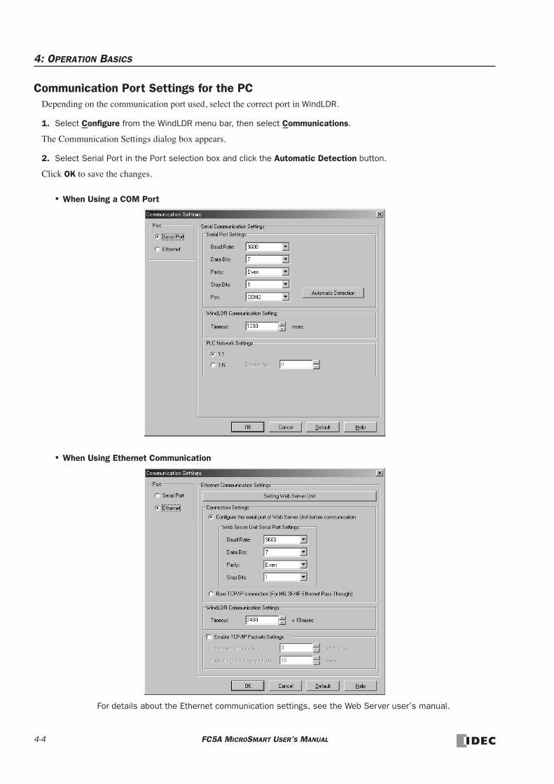
4: OPERATION BASICS
Communication Port Settings for the PCDepending on the communication port used, select the correct port in WindLDR.
1. Select Configure from the WindLDR menu bar, then select Communications.
The Communication Settings dialog box appears.
2. Select Serial Port in the Port selection box and click the Automatic Detection button.
Click OK to save the changes.
• When Using a COM Port
• When Using Ethernet Communication
For details about the Ethernet communication settings, see the Web Server user’s manual.
4-4 FC5A MICROSMART USER’S MANUAL

4: OPERATION BASICS
Start/Stop OperationThis section describes operations to start and stop the MicroSmart and to use the stop and reset inputs.
Start/Stop SchematicThe start/stop circuit of the MicroSmart consists of three blocks; power supply, M8000 (start control spe-cial internal relay), and stop/reset inputs. Each block can be used to start and stop the MicroSmart while the other two blocks are set to run the MicroSmart.
Start/Stop Operation Using WindLDRThe MicroSmart can be started and stopped using WindLDR run on a Windows PC connected to the MicroSmart CPU module. When the PLC Start button is pressed in the dialog box shown below, start control special internal relay M8000 is turned on to start the MicroSmart. When the PLC Stop button is pressed, M8000 is turned off to stop the MicroSmart.
1. Connect the PC to the MicroSmart, start WindLDR, and power up the MicroSmart. See page 4-1.
2. Check that a stop input is not designated using Configure > Function Area Settings > Run/Stop. See page 5-2.
Note: When a stop input is designated, the MicroSmart cannot be started or stopped by turning start control special inter-nal relay M8000 on or off.
3. Select Online from the WindLDR menu bar, then select Download Program. Or, click the download icon .
The Download Program dialog box appears.
4. Click the PLC Start button to start operation, then the start control special internal relay M8000 is turned on.
5. Click the PLC Stop button to stop operation, then the start control special internal relay M8000 is turned off.
The PLC operation can also be started and stopped while WindLDR is in the monitor mode. To access the Start or Stop button, select Online > Monitor and select Online > PLC Status > Run/Stop Status.
Note: Special internal relay M8000 is a keep type internal relay and stores the status when power is turned off. M8000 retains its previous status when power is turned on again. However, when the backup battery is dead, M8000 loses the stored status, and can be turned on or off as programmed when the MicroSmart is powered up. The selection is made in Configure > Function Area Settings > Run/Stop > Run/Stop Selection at Memory Backup Error. See page 5-3.
The backup duration is approximately 30 days (typical) at 25°C after the backup battery is fully charged.
• Make sure of safety before starting and stopping the MicroSmart. Incorrect operation on the MicroSmart may cause machine damage or accidents.
Caution
PowerSupply
M8000 StopInput
ResetInput
Start
Start Control
PLC
WindLDR
FC5A MICROSMART USER’S MANUAL 4-5
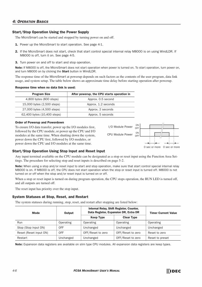
4: OPERATION BASICS
Start/Stop Operation Using the Power SupplyThe MicroSmart can be started and stopped by turning power on and off.
1. Power up the MicroSmart to start operation. See page 4-1.
2. If the MicroSmart does not start, check that start control special internal relay M8000 is on using WindLDR. If M8000 is off, turn it on. See page 4-5.
3. Turn power on and off to start and stop operation.
Note: If M8000 is off, the MicroSmart does not start operation when power is turned on. To start operation, turn power on, and turn M8000 on by clicking the Start button in WindLDR.
The response time of the MicroSmart at powerup depends on such factors as the contents of the user program, data link usage, and system setup. The table below shows an approximate time delay before starting operation after powerup.
Response time when no data link is used:
Order of Powerup and PowerdownTo ensure I/O data transfer, power up the I/O modules first, followed by the CPU module, or power up the CPU and I/O modules at the same time. When shutting down the system, power down the CPU first, followed by I/O modules, or power down the CPU and I/O modules at the same time.
Start/Stop Operation Using Stop Input and Reset InputAny input terminal available on the CPU module can be designated as a stop or reset input using the Function Area Set-tings. The procedure for selecting stop and reset inputs is described on page 5-2.
Note: When using a stop and/or reset input to start and stop operation, make sure that start control special internal relay M8000 is on. If M8000 is off, the CPU does not start operation when the stop or reset input is turned off. M8000 is not turned on or off when the stop and/or reset input is turned on or off.
When a stop or reset input is turned on during program operation, the CPU stops operation, the RUN LED is turned off, and all outputs are turned off.
The reset input has priority over the stop input.
System Statuses at Stop, Reset, and RestartThe system statuses during running, stop, reset, and restart after stopping are listed below:
Note: Expansion data registers are available on slim type CPU modules. All expansion data registers are keep types.
Program Size After powerup, the CPU starts operation in
4,800 bytes (800 steps) Approx. 0.5 second
15,000 bytes (2,500 steps) Approx. 1.2 seconds
27,000 bytes (4,500 steps) Approx. 2 seconds
62,400 bytes (10,400 steps) Approx. 5 seconds
Mode OutputInternal Relay, Shift Register, Counter, Data Register, Expansion DR, Extra DR Timer Current Value
Keep Type Clear Type
Run Operating Operating Operating Operating
Stop (Stop input ON) OFF Unchanged Unchanged Unchanged
Reset (Reset input ON) OFF OFF/Reset to zero OFF/Reset to zero Reset to zero
Restart Unchanged Unchanged OFF/Reset to zero Reset to preset
I/O Module PowerON
OFF
CPU Module PowerON
OFF
0 sec or more 0 sec or more
4-6 FC5A MICROSMART USER’S MANUAL

4: OPERATION BASICS
Simple OperationThis section describes how to edit a simple program using WindLDR on a PC, transfer the program from the PC to the MicroSmart, run the program, and monitor the operation on the WindLDR screen.
Connect the MicroSmart to the PC as described on page 4-1.
Sample User ProgramCreate a simple program using WindLDR. The sample program performs the following operation:
When only input I0 is turned on, output Q0 is turned on. When only input I1 is turned on, output Q1 is turned on. When both inputs I0 and I1 are turned on, output Q2 flashes in 1-sec increments.
Start WindLDRFrom the Start menu of Windows, select Programs > WindLDR > WindLDR.
WindLDR starts and a blank ladder editing screen appears with menus and tool bars shown on top of the screen.
Disable Tag FunctionThe following example describes a simple procedure without using the tag function.
From the WindLDR menu bar, select Configure > Ladder Preference. The Ladder Preference dialog box appears, then uncheck the check box under Tag to disuse the tag function. Click OK to close the dialog box.
Rung No. Input I0 Input I1 Output Operation
1 ON OFF Output Q0 is turned ON.
2 OFF ON Output Q1 is turned ON.
3 ON ON Output Q2 flashes in 1-sec increments.
FC5A MICROSMART USER’S MANUAL 4-7

4: OPERATION BASICS
Edit User Program Rung by RungStart the user program with the LOD instruction by inserting a NO contact of input I0.
1. Click the Normally Open contact icon .
2. Move the mouse pointer to the first column of the first line where you want to insert a NO contact, and click the left mouse button.
Note: Another method to insert a NO (or NC) contact is to move the mouse pointer where you want to insert the contact, and type A (or B).
The Normally Open dialog box appears.
3. Enter I0 in the Allocation Number field, and click OK.
A NO contact of input I0 is programmed in the first column of the first ladder line.
Next, program the ANDN instruction by inserting a NC contact of input I1.
4. Click the Normally Closed contact icon .
5. Move the mouse pointer to the second column of the first ladder line where you want to insert a NC contact, and click the left mouse button.
The Normally Closed dialog box appears.
Uncheck the Use Tag check box.
4-8 FC5A MICROSMART USER’S MANUAL
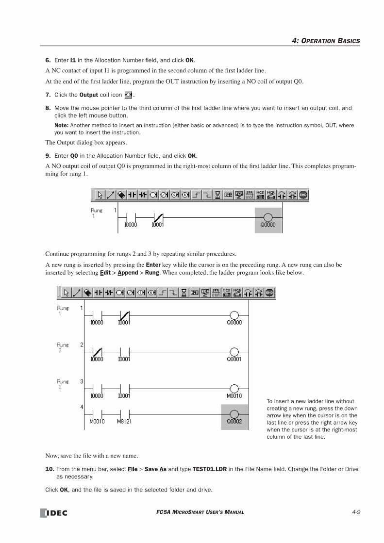
4: OPERATION BASICS
6. Enter I1 in the Allocation Number field, and click OK.
A NC contact of input I1 is programmed in the second column of the first ladder line.
At the end of the first ladder line, program the OUT instruction by inserting a NO coil of output Q0.
7. Click the Output coil icon .
8. Move the mouse pointer to the third column of the first ladder line where you want to insert an output coil, and click the left mouse button.
Note: Another method to insert an instruction (either basic or advanced) is to type the instruction symbol, OUT, where you want to insert the instruction.
The Output dialog box appears.
9. Enter Q0 in the Allocation Number field, and click OK.
A NO output coil of output Q0 is programmed in the right-most column of the first ladder line. This completes program-ming for rung 1.
Continue programming for rungs 2 and 3 by repeating similar procedures.
A new rung is inserted by pressing the Enter key while the cursor is on the preceding rung. A new rung can also be inserted by selecting Edit > Append > Rung. When completed, the ladder program looks like below.
Now, save the file with a new name.
10. From the menu bar, select File > Save As and type TEST01.LDR in the File Name field. Change the Folder or Drive as necessary.
Click OK, and the file is saved in the selected folder and drive.
To insert a new ladder line without creating a new rung, press the down arrow key when the cursor is on the last line or press the right arrow key when the cursor is at the right-most column of the last line.
FC5A MICROSMART USER’S MANUAL 4-9

4: OPERATION BASICS
Simulate OperationBefore downloading the user program, you can simulate the operation on the WindLDR screen without connecting the MicroSmart.
From the WindLDR menu bar, select Online > Simulation. The Simulation screen appears.
To change an input status, place the mouse pointer on the input and right-click the mouse. In the pop-up menu, select Set or Reset to set or reset the input.
To quit simulation, from the WindLDR menu bar, select Online > Simulation.
Download ProgramYou can download the user program from WindLDR running on a PC to the MicroSmart.
From the WindLDR menu bar, select Online > Download Program. The Download Program Dialog appears, then click the Download button. The user program is downloaded to the MicroSmart.
Note: When downloading a user program, all values and selections in the Function Area Settings are also downloaded to the MicroSmart. For Function Area Settings, see pages 5-1 through 5-38.
Download Button
4-10 FC5A MICROSMART USER’S MANUAL

4: OPERATION BASICS
Monitor OperationAnother powerful function of WindLDR is to monitor the PLC operation on the PC. The input and output statuses of the sample program can be monitored in the ladder diagram.
From the WindLDR menu bar, select Online > Monitor.
When both inputs I0 and I1 are on, the ladder diagram on the monitor screen looks as follows:
Quit WindLDRWhen you have completed monitoring, you can quit WindLDR either directly from the monitor screen or from the editing screen. In both cases, from the menu bar select File > Exit WindLDR.
Rung 1: When both inputs I0 and I1 are on, output Q0 is turned off.
Rung 2: When both inputs I0 and I1 are on, output Q1 is turned off.
Rung 3: When both input I0 and I1 are on, internal relay M10 is turned on.
M8121 is the 1-sec clock special internal relay.
While M10 is on, output Q2 flashes in 1-sec increments.
FC5A MICROSMART USER’S MANUAL 4-11

4: OPERATION BASICS
4-12 FC5A MICROSMART USER’S MANUAL

5: SPECIAL FUNCTIONS
IntroductionThe MicroSmart features special functions such as stop/reset inputs, run/stop selection at memory backup error, keep des-ignation for internal relays, shift registers, counters, and data registers. These functions are programmed using the Func-tion Area Settings menu. Also included in the Function Area Settings are high-speed counter, catch input, interrupt input, communication protocol selection for port 1 and port 2, input filter, and user program read/write protection.
This chapter describes these special functions. Clock function, analog potentiometer function, memory cartridge, and con-stant scan features are also described in this chapter.
The Function Area Settings for communication functions are detailed in chapters 17 and 27 through 31.
Function Area SettingsVarious special functions are programmed in the Function Area Settings. To call the Function Area Settings dialog box, start WindLDR on a Windows PC. From the WindLDR menu bar, select Configure > Function Area Settings. The Function Area Settings dialog box appears.
Detailed information is described on the following pages.
• Since all Function Area Settings relate to the user program, the user program must be downloaded to the MicroSmart after changing any of these settings.
Caution
Input filter, clock cartridge adjustment, user program read/write protection, AS-Interface master, memory cartridge, extra data register D10000-D49999 settings
Communication mode setting for port 1 and port 2 to use maintenance, user, modem, data link master/slave, and Modbus communication
Normal input, two/single-phase high-speed counter, catch input, or interrupt input
Keep/clear designation for internal relays, shift registers, counters, and data registers
Stop/reset inputs and run/stop selection at memory backup error
Resets all Function Area Settings values to defaults.
FC5A MICROSMART USER’S MANUAL 5-1

5: SPECIAL FUNCTIONS
Stop Input and Reset InputAs described on page 4-5, the MicroSmart can be started and stopped using a stop input or reset input, which can be desig-nated from the Function Area Settings menu. When the designated stop or reset input is turned on, the MicroSmart stops operation. For the system statuses in the stop and reset modes, see page 4-6.
Since these settings relate to the user program, the user program must be downloaded to the MicroSmart after changing any of these settings.
Programming WindLDR
1. From the WindLDR menu bar, select Configure > Function Area Settings. The Function Area Settings dialog box appears.
2. Select the Run/Stop tab.
Stop Input: Click the check box on the left of Use Stop Input and type a desired input number available on the CPU module in the Stop Input field.
Reset Input: Click the check box on the left of Use Reset Input and type a desired reset number available on the CPU module in the Reset Input field.
Default: No stop and reset inputs are designated.
3. Click the OK button.
This example designates input I0 as a stop input and input I1 as a reset input.
5-2 FC5A MICROSMART USER’S MANUAL

5: SPECIAL FUNCTIONS
Run/Stop Selection at Memory Backup ErrorStart control special internal relay M8000 maintains its status when the CPU is powered down. After the CPU has been off for a period longer than the battery backup duration, the data designated to be maintained during power failure is broken. The Run/Stop Selection at Memory Backup Error dialog box is used to select whether to start or stop the CPU when attempting to restart operation after the “keep” data in the CPU RAM has been lost.
When a built-in lithium battery is fully charged, data of internal relays, shift registers, counters, and data registers stored in the RAM are maintained for approximately 30 days.
Since this setting relates to the user program, the user program must be downloaded to the MicroSmart after changing this setting.
Programming WindLDR
1. From the WindLDR menu bar, select Configure > Function Area Settings. The Function Area Settings dialog box appears.
2. Select the Run/Stop tab.
Run (Default): Click the button on the left to start the CPU at memory backup error.
Stop: Click the button on the right to stop the CPU when attempting to start at memory backup error. When the CPU does not start because of the Stop selection, the CPU can not be started alone, then the CPU can still be started by sending a start command from WindLDR to turn on start control spe-cial internal relay M8000. For start/stop operation, see page 4-5.
3. Click the OK button.
FC5A MICROSMART USER’S MANUAL 5-3

5: SPECIAL FUNCTIONS
Keep Designation for Internal Relays, Shift Registers, Counters, and Data RegistersThe statuses of internal relays and shift register bits are usually cleared at startup. It is also possible to designate all or a block of consecutive internal relays or shift register bits as “keep” types. Counter current values and data register values are usually maintained at powerup. It is also possible to designate all or a block of consecutive counters and data registers as “clear” types.
When the CPU is stopped, these statuses and values are maintained. When the CPU is reset by turning on a designated reset input, these statues and values are cleared despite the settings in the Keep dialog box shown below. The keep/clear settings in this dialog box have effect when restarting the CPU.
Since these settings relate to the user program, the user program must be downloaded to the MicroSmart after changing any of these settings.
Programming WindLDR
1. From the WindLDR menu bar, select Configure > Function Area Settings. The Function Area Settings dialog box appears.
2. Select the Keep tab. The Keep page appears.
5-4 FC5A MICROSMART USER’S MANUAL
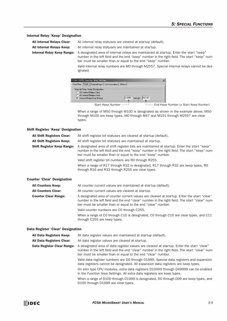
5: SPECIAL FUNCTIONS
Internal Relay ‘Keep’ Designation
All Internal Relays Clear: All internal relay statuses are cleared at startup (default).
All Internal Relays Keep: All internal relay statuses are maintained at startup.
Internal Relay Keep Range: A designated area of internal relays are maintained at startup. Enter the start “keep” number in the left field and the end “keep” number in the right field. The start “keep” num-ber must be smaller than or equal to the end “keep” number.
Valid internal relay numbers are M0 through M2557. Special internal relays cannot be des-ignated.
When a range of M50 through M100 is designated as shown in the example above, M50 through M100 are keep types, M0 through M47 and M101 through M2557 are clear types.
Shift Register ‘Keep’ Designation
All Shift Registers Clear: All shift register bit statuses are cleared at startup (default).
All Shift Registers Keep: All shift register bit statuses are maintained at startup.
Shift Register Keep Range: A designated area of shift register bits are maintained at startup. Enter the start “keep” number in the left field and the end “keep” number in the right field. The start “keep” num-ber must be smaller than or equal to the end “keep” number.
Valid shift register bit numbers are R0 through R255.
When a range of R17 through R32 is designated, R17 through R32 are keep types, R0 through R16 and R33 through R255 are clear types.
Counter ‘Clear’ Designation
All Counters Keep: All counter current values are maintained at startup (default).
All Counters Clear: All counter current values are cleared at startup.
Counter Clear Range: A designated area of counter current values are cleared at startup. Enter the start “clear” number in the left field and the end “clear” number in the right field. The start “clear” num-ber must be smaller than or equal to the end “clear” number.
Valid counter numbers are C0 through C255.
When a range of C0 through C10 is designated, C0 through C10 are clear types, and C11 through C255 are keep types.
Data Register ‘Clear’ Designation
All Data Registers Keep: All data register values are maintained at startup (default).
All Data Registers Clear: All data register values are cleared at startup.
Data Register Clear Range: A designated area of data register values are cleared at startup. Enter the start “clear” number in the left field and the end “clear” number in the right field. The start “clear” num-ber must be smaller than or equal to the end “clear” number.
Valid data register numbers are D0 through D1999. Special data registers and expansion data registers cannot be designated. All expansion data registers are keep types.
On slim type CPU modules, extra data registers D10000 through D49999 can be enabled in the Function Area Settings. All extra data registers are keep types.
When a range of D100 through D1999 is designated, D0 through D99 are keep types, and D100 through D1999 are clear types.
Start Keep Number End Keep Number (≥ Start Keep Number)
FC5A MICROSMART USER’S MANUAL 5-5

5: SPECIAL FUNCTIONS
High-speed CounterThis section describes the high-speed counter function to count many pulse inputs within one scan. Using the built-in 16-bit high-speed counter, the all-in-one type CPU module counts up to 65,535 high-speed pulses. Using the built-in 32-bit high-speed counter, the slim type CPU module counts up 4,294,967,295 pulses.
The high-speed counter counts input pulses from a rotary encoder or proximity switch without regard to the scan time, compares the current value with a preset value, and turns on the output when the current value reaches the preset value. This function can be used for simple motor control or to measure lengths of objects.
The all-in-one type CPU modules and slim type CPU modules have different high-speed counter configurations.
High-speed counters are programmed in the Function Area Settings in WindLDR and allocated to input terminals I0 through I5 (all-in-one type CPU module) or I7 (slim type CPU module) in four groups. When high-speed counters are used, input terminals in the same group cannot be used for ordinary inputs, catch inputs, or interrupt inputs.
CPU Module All-in One Type CPU Module
High-speed Counter No. HSC1 HSC2, HSC3, HSC4
Operation Mode Single-phase Two-phase Single-phase
Counting Mode Adding counter 1-edge count Adding counter
Maximum Counting Frequency 50 kHz 5 kHz
Counting Range 0 to 65,535 (16 bits)
Current Value Comparison Preset valueOverflow
UnderflowPreset value
Comparison Action Comparison output
Reset Input With Without
Reset Special Internal Relay With
Current Value after Reset 0 Reset value 0
CPU Module Slim Type CPU Module
High-speed Counter No. HSC1, HSC4 HSC2, HSC3
Operation Mode Single-phase Two-phase Single-phase
Counting ModeAdding counter Dual-pulse reversible Up/down selection reversible
1-edge count 2-edge count 4-edge count
Adding counter
Maximum Counting Frequency 100 kHz1-edge count: 100 kHz 2-edge count: 50 kHz 4-edge count: 25 kHz
100 kHz
Counting Range 0 to 4,294,967,295 (32 bits)
Current Value Comparison
Preset value 1Preset value 2
OverflowUnderflow
Preset value
Comparison ActionComparison outputInterrupt program
Reset Input With Without
Reset Special Internal Relay With
Current Value after Reset Reset value 0
5-6 FC5A MICROSMART USER’S MANUAL

5: SPECIAL FUNCTIONS
High-speed Counters on All-in-One Type CPU ModulesAll-in-one type CPU modules have four 16-bit high-speed counters; HSC1 through HSC4, which can count up to 65,535. HSC1 can be used as a single-phase or two-phase 50-kHz high-speed counter. HSC2 through HSC4 are single-phase 5-kHz high-speed counters. All high-speed counter functions are selected using the Function Area Settings in WindLDR.
High-speed Counter Operation Modes and Input Terminals (All-in-One Type CPU Modules)High-speed counters HSC1 through HSC4 are allocated input terminals as listed in the following table.
Note 1: When the voltage difference between the input terminal and the COM terminal is 24V DC, the input turns on. Both positive and negative input voltages are accepted. Note 2: Input I0 can be used as an ordinary input terminal. Note 3: When a reset input is not used, input I2 can be used as an ordinary input terminal.
Single-phase High-speed Counters HSC1 through HSC4 (All-in-One Type CPU Modules)HSC1 can be used as a single-phase high-speed counter as well as HSC2 through HSC4. The four single-phase high-speed counters count input pulses to the input terminal allocated to each high-speed counter. When the preset value is reached, a designated comparison output turns on, and the current value is reset to 0 to count subsequent input pulses.
Five special internal relays and two special data registers are assigned to control and monitor each single-phase high-speed counter operation. The current value is stored in a special data register (current value) and is updated every scan. The value stored in another special data register (preset value) is used as a preset value. When a reset input special internal relay is turned on, the current value is reset to 0.
The single-phase high-speed counter is enabled while a gate input special internal relay is on and is disabled while the gate input is off. When the current value reaches the preset value, a special internal relay (comparison ON status) turns on in the next scan. At this point, the current value is reset to 0, and the value stored in a preset value special data register takes effect for the subsequent counting cycle. When a comparison output reset special internal relay is turned on, the designated comparison output is turned off.
In addition, only the single-phase high-speed counter HSC1 has reset input I2 and reset status special internal relay M8130. When reset input I2 is turned on to reset the current value to 0, reset status special internal relay M8130 turns on in the next scan. When reset input special internal relay M8032 is turned on, M8130 does not turn on. See page 5-8.
Special Internal Relays for Single-phase High-speed Counters (All-in-One Type CPU Modules)
Note: Special internal relays M8130, M8131, M8133, M8134, and M8136 go on for only one scan.
Special Data Registers for Single-phase High-speed Counters (All-in-One Type CPU Modules)
High-speed Counter No. HSC1 HSC2 HSC3 HSC4
Input Terminal (Note 1) I0 I1 I2 I3 I4 I5
Single-phase High-speed Counter (Note 2) Pulse InputReset Input
(Note 3)Pulse Input Pulse Input Pulse Input
Two-phase High-speed Counter Phase A Phase BReset Input(Phase Z)(Note 3)
— — —
DescriptionHigh-speed Counter No.
ON Read/WriteHSC1 HSC2 HSC3 HSC4
Comparison Output Reset M8030 M8034 M8040 M8044 Turns off comparison output R/W
Gate Input M8031 M8035 M8041 M8045 Enables counting R/W
Reset Input M8032 M8036 M8042 M8046 Resets the current value R/W
Reset Status M8130 — — — Current value reset by I2 Read only
Comparison ON Status M8131 M8133 M8134 M8136 Preset value reached Read only
DescriptionHigh-speed Counter No.
Updated Read/WriteHSC1 HSC2 HSC3 HSC4
High-speed Counter Current Value D8045 D8047 D8049 D8051 Every scan Read only
High-speed Counter Preset Value D8046 D8048 D8050 D8052 — R/W
FC5A MICROSMART USER’S MANUAL 5-7

5: SPECIAL FUNCTIONS
Single-phase High-speed Counter Functions (All-in-One Type CPU Modules)
Single-phase High-speed Counter Timing Chart
Example: Single--phase high-speed counter HSC2Preset value is 8. Q0 is designated as a comparison output.
Counting Mode Adding counter
Maximum Counting FrequencyHSC1: 50 kHz HSC2 through HSC4: 5 kHz
Counting Range 0 to 65535 (16 bits)
Gate Control Enable/disable counting
Current Value ResetCurrent value is reset to 0 when the current value reaches the preset value or when reset input I2 (HSC1 only) or a reset input special internal relay is turned on.
Status Relays Special internal relays for indicating high-speed counter statuses.
Comparison Output
Any output number available on the CPU module can be designated as a comparison output which turns on when the current value reaches the preset value.Output numbers on expansion output or mixed I/O modules cannot be designated as a comparison output.
Reset Input M8036
012
8
Current Value D8047
The D8048 value at this point becomes the preset value for the next counting cycle.
Pulse Input I3
Gate Input M8035
Comparison Output Q0
Comparison Output Reset M8034
1 scan timeComparison ON Status M8133
76543
• When reset input M8036 is turned on, the D8047 current value is cleared to 0, then the D8048 preset value takes effect for the next counting cycle.
• While gate input M8035 is on, single-phase high-speed counter HSC2 counts pulse inputs to input I3.
• The D8047 current value is updated every scan.
• When the D8047 current value reaches the D8048 preset value, comparison ON status M8133 goes on for one scan. At the same time, comparison output Q0 turns on and remains on until comparison output reset M8034 is turned on.
• When the D8047 current value reaches the D8048 preset value, the D8048 preset value at that point takes effect for the next counting cycle.
Preset Value D8048 8
5-8 FC5A MICROSMART USER’S MANUAL

5: SPECIAL FUNCTIONS
Two-phase High-speed Counter HSC1 (All-in-One Type CPU Modules)Two-phase high-speed counter HSC1 operates in the rotary encoder mode, and counts up or down input pulses to input ter-minals I0 (phase A) and I1 (phase B). When the current value overflows 65535 or underflows 0, a designated comparison output turns on. Any output terminal available on the CPU module can be designated as a comparison output. When input I2 (reset input) is turned on, the current value is reset to a predetermined reset value, and the two-phase high-speed counter counts subsequent input pulses starting at the reset value.
Six special internal relays and two special data registers are assigned to control and monitor the two-phase high-speed counter operation. The current value is stored in data register D8045 (current value) and is updated every scan. The value stored in D8046 (reset value) is used as a reset value. When a high-speed counter reset input (I2 or M8032) is turned on, the current value in D8045 is reset to the value stored in D8046.
The two-phase high-speed counter is enabled while gate input special internal relay M8031 is on and is disabled while M8031 is off. When current value overflow or underflow occurs while counting up or down, special internal relay M8131 or M8132 turns on in the next scan, respectively. At this point, the D8045 current value is reset to the D8046 reset value for the subsequent counting cycle. When comparison output reset special internal relay M8030 is turned on, the designated comparison output is turned off. When reset input I2 is turned on to reset the current value, reset status special internal relay M8130 turns on in the next scan. When reset input special internal relay M8032 is turned on, M8130 does not turn on. See page 5-10.
Special Internal Relays for Two-phase High-speed Counter (All-in-One Type CPU Modules)
Note: Special internal relays M8130 through M8132 go on for only one scan.
Special Data Registers for Two-phase High-speed Counter (All-in-One Type CPU Modules)
Two-phase High-speed Counter Functions (All-in-One Type CPU Modules)
DescriptionHigh-speed Counter No.
ON Read/WriteHSC1 HSC2 HSC3 HSC4
Comparison Output Reset M8030 — — — Turns off comparison output R/W
Gate Input M8031 — — — Enables counting R/W
Reset Input M8032 — — — Resets the current value R/W
Reset Status M8130 — — — Current value reset by I2 Read only
Current Value Overflow M8131 — — — Overflow occurred Read only
Current Value Underflow M8132 — — — Underflow occurred Read only
DescriptionHigh-speed Counter No.
Updated Read/WriteHSC1 HSC2 HSC3 HSC4
High-speed Counter Current Value D8045 — — — Every scan Read only
High-speed Counter Reset Value D8046 — — — — R/W
Counting Mode 1-edge count (phases A, B, Z)
Maximum Counting Frequency 50 kHz
Counting Range 0 to 65535 (16 bits)
Gate Control Enable/disable counting
Current Value ResetCurrent value is reset to a given value when the current value overflows 65535 or underflows 0, or when reset input I2 or reset input special internal relay M8032 is turned on.
Control/Status RelaysSpecial internal relays are provided to control and monitor the high-speed counter operation.
Comparison Output
Any output number available on the CPU module can be designated as a comparison output which turns on when current value overflow or underflow occurs.Output numbers on expansion output or mixed I/O modules cannot be designated as a comparison output.
FC5A MICROSMART USER’S MANUAL 5-9

5: SPECIAL FUNCTIONS
Two-phase High-speed Counter Timing Chart
Example: Two--phase high-speed counter HSC1Reset input I2 is used. Q1 is designated as a comparison output.
Reset Input I2
Reset Value D8046
012
8
Current Value D8045
1 scan time
The D8046 value at this point becomes the reset value for the next counting cycle.
Phase A Input I0
Phase B Input I1
655335
Reset Status M8130
3
Gate Input M8031
Comparison Output Q1
Comparison Output Reset M8030
1 scan timeCurrent Value Overflow M8131
1 scan timeCurrent Value Underflow M8132
76543
65532655336553465535
Underflow Overflow
• When reset input I2 is turned on, the D8046 reset value is set to the D8045 current value, then reset status M8130 turns on for one scan. If reset input M8032 is turned on, reset status M8130 does not turn on.
• While gate input M8031 is on, the two-phase high-speed counter counts up or down depending on the phase dif-ference between phase A (input I0) and phase B (input I1).
Phase A (Input I0)
Phase B (Input I1)
Count Up (Increment)
Phase A (Input I0)
Phase B (Input I1)
Count Down (Decrement)
5-10 FC5A MICROSMART USER’S MANUAL
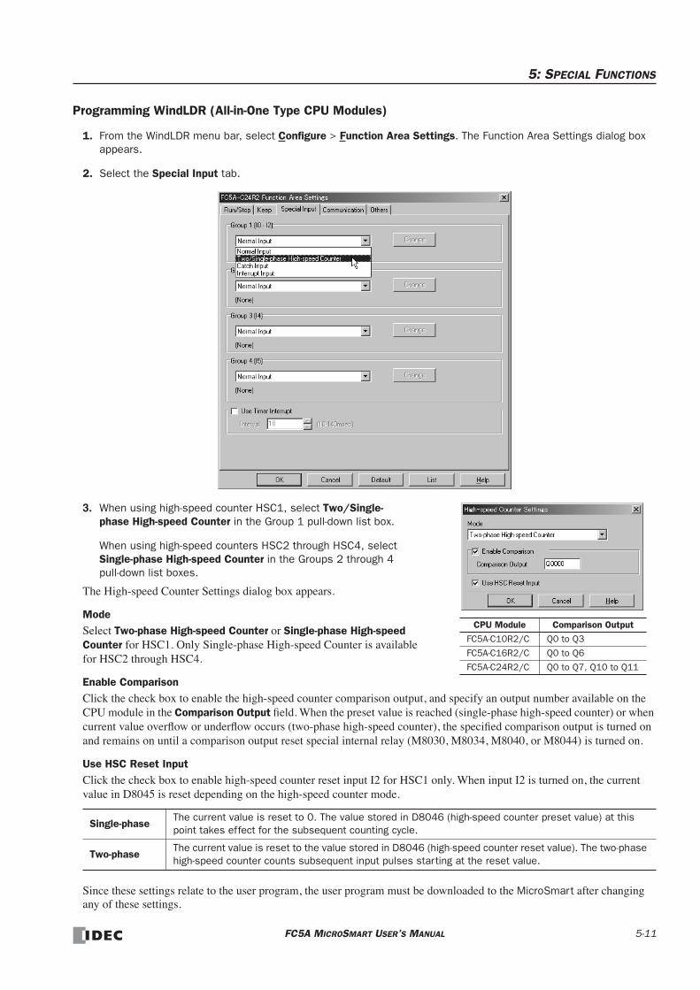
5: SPECIAL FUNCTIONS
Programming WindLDR (All-in-One Type CPU Modules)
1. From the WindLDR menu bar, select Configure > Function Area Settings. The Function Area Settings dialog box appears.
2. Select the Special Input tab.
3. When using high-speed counter HSC1, select Two/Single-phase High-speed Counter in the Group 1 pull-down list box.
When using high-speed counters HSC2 through HSC4, select Single-phase High-speed Counter in the Groups 2 through 4 pull-down list boxes.
The High-speed Counter Settings dialog box appears.
ModeSelect Two-phase High-speed Counter or Single-phase High-speed Counter for HSC1. Only Single-phase High-speed Counter is available for HSC2 through HSC4.
Enable ComparisonClick the check box to enable the high-speed counter comparison output, and specify an output number available on the CPU module in the Comparison Output field. When the preset value is reached (single-phase high-speed counter) or when current value overflow or underflow occurs (two-phase high-speed counter), the specified comparison output is turned on and remains on until a comparison output reset special internal relay (M8030, M8034, M8040, or M8044) is turned on.
Use HSC Reset InputClick the check box to enable high-speed counter reset input I2 for HSC1 only. When input I2 is turned on, the current value in D8045 is reset depending on the high-speed counter mode.
Since these settings relate to the user program, the user program must be downloaded to the MicroSmart after changing any of these settings.
Single-phaseThe current value is reset to 0. The value stored in D8046 (high-speed counter preset value) at this point takes effect for the subsequent counting cycle.
Two-phaseThe current value is reset to the value stored in D8046 (high-speed counter reset value). The two-phase high-speed counter counts subsequent input pulses starting at the reset value.
CPU Module Comparison Output
FC5A-C10R2/C Q0 to Q3
FC5A-C16R2/C Q0 to Q6
FC5A-C24R2/C Q0 to Q7, Q10 to Q11
FC5A MICROSMART USER’S MANUAL 5-11
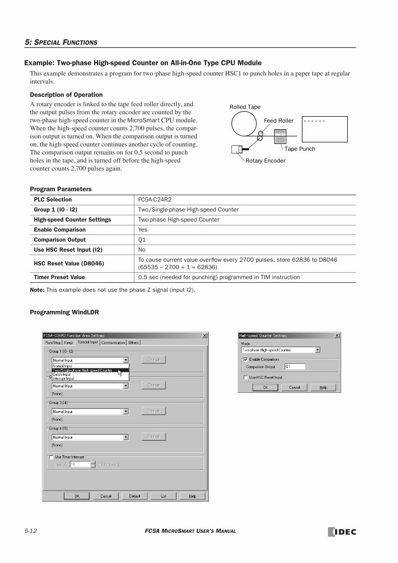
5: SPECIAL FUNCTIONS
Example: Two-phase High-speed Counter on All-in-One Type CPU ModuleThis example demonstrates a program for two-phase high-speed counter HSC1 to punch holes in a paper tape at regular intervals.
Description of OperationA rotary encoder is linked to the tape feed roller directly, and the output pulses from the rotary encoder are counted by the two-phase high-speed counter in the MicroSmart CPU module. When the high-speed counter counts 2,700 pulses, the compar-ison output is turned on. When the comparison output is turned on, the high-speed counter continues another cycle of counting. The comparison output remains on for 0.5 second to punch holes in the tape, and is turned off before the high-speed counter counts 2,700 pulses again.
Program Parameters
Note: This example does not use the phase Z signal (input I2).
Programming WindLDR
PLC Selection FC5A-C24R2
Group 1 (I0 - I2) Two/Single-phase High-speed Counter
High-speed Counter Settings Two-phase High-speed Counter
Enable Comparison Yes
Comparison Output Q1
Use HSC Reset Input (I2) No
HSC Reset Value (D8046)To cause current value overflow every 2700 pulses, store 62836 to D8046 (65535 – 2700 + 1 = 62836)
Timer Preset Value 0.5 sec (needed for punching) programmed in TIM instruction
Feed Roller
Rotary Encoder
Tape Punch
Rolled Tape
5-12 FC5A MICROSMART USER’S MANUAL

5: SPECIAL FUNCTIONS
Ladder DiagramWhen the MicroSmart starts operation, reset value 62836 is stored to reset value special data register D8046. Gate input special internal relay M8031 is turned on at the end of the third scan to start the high-speed counter to count input pulses.
Timing Chart
M8120
M8120 is the initialize pulse special internal relay.
1st scan SUB and ADD instructions are used to store a reset value of 62836 (65535 – 2700 + 1) to D8046 (reset value).
M8031 (gate input) is turned off.
M0 is turned off.
3rd scan At the rising edge of M0, M8031 (gate input) is turned on. After the END processing of the third scan, HSC1 starts counting.
2nd scan At the falling edge of M8120 (initialize pulse), M0 is turned on. M8032 (reset input) is turned on to initialize HSC1 in the END pro-cessing of the second scan.
When HSC1 overflows 65535, output Q1 (comparison output) is turned on to start timer T0. HSC1 starts to repeat counting.
When the timer times out 0.5 sec, M8030 (comparison output reset) is turned on to turn off output Q1.END
M0
M8031R
M8031SSOTU
REPS2 –2700
D1 –D0
S1 –65535
SUB(W)
REPS2 –1
D1 –D8046
S1 –D0
ADD(W)
M0R
M8120 M0SSOTD
Q1TIM5
T0M8030
M8032
Comparison Output Q1ON
OFF
Current Value D8045
When the high-speed counter current value exceeds 65535, comparison output Q1 is turned on and the current value is reset to 62836.
Reset Value D8046 62836
65535
0.5 sec for punching
2700 pulses
FC5A MICROSMART USER’S MANUAL 5-13

5: SPECIAL FUNCTIONS
High-speed Counters on Slim Type CPU ModulesSlim type CPU modules have four 32-bit high-speed counters, HSC1 through HSC4, which can count up to 4,294,967,295 pulses. HSC1 and HSC4 can be used as a single-phase or two-phase high-speed counter. HSC2 and HSC3 are single-phase high-speed counters. All high-speed counter functions are selected using the Function Area Settings in WindLDR.
High-speed Counter Operation Modes and Input Terminals (Slim Type CPU Modules)
Note 1: When the voltage difference between the input terminal and the COM terminal is 24V DC, the input turns on. Both positive and negative input voltages are accepted. Note 2: In the single-phase high-speed counter, inputs I0 and I6 are used for dual-pulse reversible counters and up/down selection reversible counters. When adding counter is selected, inputs I0 and I6 can be used as ordinary input terminals. Note 3: When a reset input is not used, inputs I2 and I5 can be used as an ordinary input terminal.
Single-phase High-speed Counters HSC1 through HSC4 (Slim Type CPU Modules)Single-phase counters include three modes; adding counter, dual-pulse reversible counter, and up/down selection revers-ible counter. All high-speed counters HSC1 through HSC4 can be used as adding counters. HSC1 and HSC4 can also be used as a dual-pulse reversible counter and an up/down selection reversible counter.
Adding CounterThe four adding counters count input pulses to the input terminal allocated to each high-speed counter.
HSC1 and HSC4 can designate two preset values: preset value 1 and preset value 2. When the current value reaches preset value 1, a designated comparison output turns on or program execution jumps to a designated tag. At this point, the current value can be designated to keep counting subsequent input pulses or to be reset to the reset value and restart another count-ing cycle. When “Keep Current Value” is designated, the current value continues to increase up to preset value 2, then another comparison output can be turned on or program execution jumps to a designated tag. Similarly, when “Keep Cur-rent Value” is designated for preset value 2, the current value continues to increase up to 4,294,967,295. At this point, another comparison output can be turned on or program execution jumps to a designated tag, and the current value is reset to the reset value.
HSC2 and HSC3 can designate one preset value. When the preset value is reached, a designated comparison output turns on or program execution jumps to a designated tag, and the current value is reset to 0 to start another counting cycle.
Dual-pulse Reversible CounterHSC1 and HSC4 can also be used as dual-pulse reversible counters to increment or decrement the current value when receiving input pulses to the up pulse input terminal or the down pulse input terminal, respectively.
HSC No. HSC1 HSC2 HSC3 HSC4
Input Terminal (Note 1) I0 I1 I2 I3 I4 I5 I6 I7
Single-phase High-speed Counter
Adding Counter (Note 2)Pulse Input
Reset Input(Note 3)
Pulse Input
Pulse Input
Reset Input(Note 3)
(Note 2)Pulse Input
Dual-pulse Reversible Counter
Down Pulse
Up Pulse
Reset Input(Note 3)
— —Reset Input
(Note 3)Down Pulse
Up Pulse
Up/down Selection Reversible Counter
U/D Selection
Pulse Input
Reset Input(Note 3)
— —Reset Input
(Note 3)U/D
SelectionPulse Input
Two-phase High-speed Counter
1-edge Count2-edge Count4-edge Count
Phase A Phase BReset Input(Phase Z)(Note 3)
— —Reset Input(Phase Z)(Note 3)
Phase A Phase B
Pulse Input
10 11 12 13 14
ON
OFF
Current Value
When the pulse input turns on, the current value increments.
• Single-phase Adding Counter Operation Chart
5-14 FC5A MICROSMART USER’S MANUAL
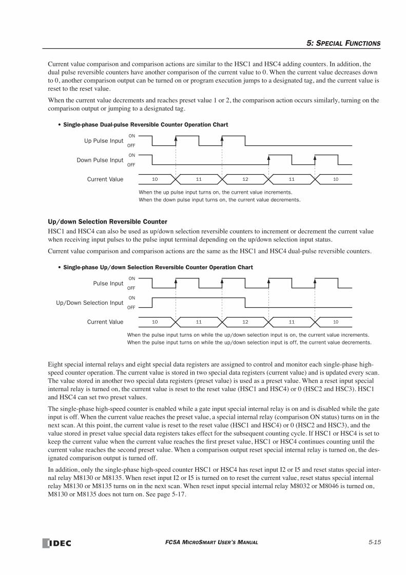
5: SPECIAL FUNCTIONS
Current value comparison and comparison actions are similar to the HSC1 and HSC4 adding counters. In addition, the dual pulse reversible counters have another comparison of the current value to 0. When the current value decreases down to 0, another comparison output can be turned on or program execution jumps to a designated tag, and the current value is reset to the reset value.
When the current value decrements and reaches preset value 1 or 2, the comparison action occurs similarly, turning on the comparison output or jumping to a designated tag.
Up/down Selection Reversible CounterHSC1 and HSC4 can also be used as up/down selection reversible counters to increment or decrement the current value when receiving input pulses to the pulse input terminal depending on the up/down selection input status.
Current value comparison and comparison actions are the same as the HSC1 and HSC4 dual-pulse reversible counters.
Eight special internal relays and eight special data registers are assigned to control and monitor each single-phase high-speed counter operation. The current value is stored in two special data registers (current value) and is updated every scan. The value stored in another two special data registers (preset value) is used as a preset value. When a reset input special internal relay is turned on, the current value is reset to the reset value (HSC1 and HSC4) or 0 (HSC2 and HSC3). HSC1 and HSC4 can set two preset values.
The single-phase high-speed counter is enabled while a gate input special internal relay is on and is disabled while the gate input is off. When the current value reaches the preset value, a special internal relay (comparison ON status) turns on in the next scan. At this point, the current value is reset to the reset value (HSC1 and HSC4) or 0 (HSC2 and HSC3), and the value stored in preset value special data registers takes effect for the subsequent counting cycle. If HSC1 or HSC4 is set to keep the current value when the current value reaches the first preset value, HSC1 or HSC4 continues counting until the current value reaches the second preset value. When a comparison output reset special internal relay is turned on, the des-ignated comparison output is turned off.
In addition, only the single-phase high-speed counter HSC1 or HSC4 has reset input I2 or I5 and reset status special inter-nal relay M8130 or M8135. When reset input I2 or I5 is turned on to reset the current value, reset status special internal relay M8130 or M8135 turns on in the next scan. When reset input special internal relay M8032 or M8046 is turned on, M8130 or M8135 does not turn on. See page 5-17.
Down Pulse Input
10 11 12 11 10
ON
OFF
Current Value
When the up pulse input turns on, the current value increments.When the down pulse input turns on, the current value decrements.
• Single-phase Dual-pulse Reversible Counter Operation Chart
Up Pulse InputON
OFF
Up/Down Selection Input
10 11 12 11 10
ON
OFF
Current Value
When the pulse input turns on while the up/down selection input is on, the current value increments.When the pulse input turns on while the up/down selection input is off, the current value decrements.
• Single-phase Up/down Selection Reversible Counter Operation Chart
Pulse InputON
OFF
FC5A MICROSMART USER’S MANUAL 5-15
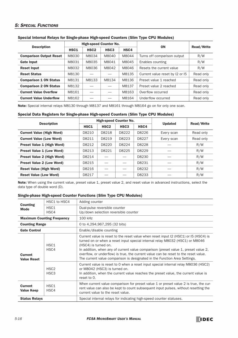
5: SPECIAL FUNCTIONS
Special Internal Relays for Single-phase High-speed Counters (Slim Type CPU Modules)
Note: Special internal relays M8130 through M8137 and M8161 through M8164 go on for only one scan.
Special Data Registers for Single-phase High-speed Counters (Slim Type CPU Modules)
Note: When using the current value, preset value 1, preset value 2, and reset value in advanced instructions, select the data type of double word (D).
Single-phase High-speed Counter Functions (Slim Type CPU Modules)
DescriptionHigh-speed Counter No.
ON Read/WriteHSC1 HSC2 HSC3 HSC4
Comparison Output Reset M8030 M8034 M8040 M8044 Turns off comparison output R/W
Gate Input M8031 M8035 M8041 M8045 Enables counting R/W
Reset Input M8032 M8036 M8042 M8046 Resets the current value R/W
Reset Status M8130 — — M8135 Current value reset by I2 or I5 Read only
Comparison 1 ON Status M8131 M8133 M8134 M8136 Preset value 1 reached Read only
Comparison 2 ON Status M8132 — — M8137 Preset value 2 reached Read only
Current Value Overflow M8161 — — M8163 Overflow occurred Read only
Current Value Underflow M8162 — — M8164 Underflow occurred Read only
DescriptionHigh-speed Counter No.
Updated Read/WriteHSC1 HSC2 HSC3 HSC4
Current Value (High Word) D8210 D8218 D8222 D8226 Every scan Read only
Current Value (Low Word) D8211 D8219 D8223 D8227 Every scan Read only
Preset Value 1 (High Word) D8212 D8220 D8224 D8228 — R/W
Preset Value 1 (Low Word) D8213 D8221 D8225 D8229 — R/W
Preset Value 2 (High Word) D8214 — — D8230 — R/W
Preset Value 2 (Low Word) D8215 — — D8231 — R/W
Reset Value (High Word) D8216 — — D8232 — R/W
Reset Value (Low Word) D8217 — — D8233 — R/W
Counting Mode
HSC1 to HSC4 Adding counter
HSC1HSC4
Dual-pulse reversible counter Up/down selection reversible counter
Maximum Counting Frequency 100 kHz
Counting Range 0 to 4,294,967,295 (32 bits)
Gate Control Enable/disable counting
Current Value Reset
HSC1HSC4
Current value is reset to the reset value when reset input I2 (HSC1) or I5 (HSC4) is turned on or when a reset input special internal relay M8032 (HSC1) or M8046 (HSC4) is turned on. In addition, when any of current value comparison (preset value 1, preset value 2, overflow, or underflow) is true, the current value can be reset to the reset value. The current value comparison is designated in the Function Area Settings.
HSC2HSC3
Current value is reset to 0 when a reset input special internal relay M8036 (HSC2) or M8042 (HSC3) is turned on. In addition, when the current value reaches the preset value, the current value is reset to 0.
Current Value Keep
HSC1HSC4
When current value comparison for preset value 1 or preset value 2 is true, the cur-rent value can also be kept to count subsequent input pulses, without resetting the current value to the reset value.
Status Relays Special internal relays for indicating high-speed counter statuses.
5-16 FC5A MICROSMART USER’S MANUAL
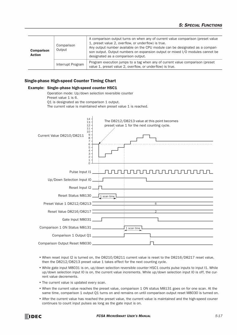
5: SPECIAL FUNCTIONS
Single-phase High-speed Counter Timing Chart
Example: Single--phase high-speed counter HSC1 Operation mode: Up/down selection reversible counter Preset value 1 is 6. Q1 is designated as the comparison 1 output. The current value is maintained when preset value 1 is reached.
Comparison Action
Comparison Output
A comparison output turns on when any of current value comparison (preset value 1, preset value 2, overflow, or underflow) is true.Any output number available on the CPU module can be designated as a compari-son output. Output numbers on expansion output or mixed I/O modules cannot be designated as a comparison output.
Interrupt ProgramProgram execution jumps to a tag when any of current value comparison (preset value 1, preset value 2, overflow, or underflow) is true.
1 scan time
1 scan time
Reset Input I2
89
10
Current Value D8210/D8211
The D8212/D8213 value at this point becomes preset value 1 for the next counting cycle.
Pulse Input I1
Gate Input M8031
Comparison 1 ON Status M8131
Comparison 1 Output Q1
Comparison Output Reset M8030
14131211
• When reset input I2 is turned on, the D8210/D8211 current value is reset to the D8216/D8217 reset value, then the D8212/D8213 preset value 1 takes effect for the next counting cycle.
• While gate input M8031 is on, up/down selection reversible counter HSC1 counts pulse inputs to input I1. While up/down selection input I0 is on, the current value increments. While up/down selection input I0 is off, the cur-rent value decrements.
• The current value is updated every scan.
• When the current value reaches the preset value, comparison 1 ON status M8131 goes on for one scan. At the same time, comparison 1 output Q1 turns on and remains on until comparison output reset M8030 is turned on.
• After the current value has reached the preset value, the current value is maintained and the high-speed couner continues to count input pulses as long as the gate input is on.
Preset Value 1 D8212/D8213 6
012
76543
Up/Down Selection Input I0
Reset Status M8130
Reset Value D8216/D8217 2
FC5A MICROSMART USER’S MANUAL 5-17

5: SPECIAL FUNCTIONS
Two-phase High-speed Counters HSC1 and HSC4 (Slim Type CPU Modules)Two-phase high-speed counters HSC1 and HSC4 operates in the rotary encoder mode, and counts up or down input pulses to input terminals I0 or I6 (phase A) and I1 or I7 (phase B), respectively.
HSC1 and HSC4 can designate two preset values: preset value 1 and preset value 2. When the current value reaches preset value 1, a designated comparison output turns on or program execution jumps to a designated tag. At this point, the current value can be designated to keep counting subsequent input pulses or to be reset to the reset value and restart another count-ing cycle. When “Keep Current Value” is designated, the current value continues to increase up to preset value 2, then another comparison output can be turned on or program execution jumps to a designated tag. Similarly, when “Keep Cur-rent Value” is designated for preset value 2, the current value continues to increase up to 4,294,967,295. At this point, another comparison output can be turned on or program execution jumps to a designated tag, and the current value is reset to the reset value.
In addition, the two-phase high-speed counters have another comparison of the current value to 0. When the current value decreases down to 0, another comparison output can be turned on or program execution jumps to a designated tag, and the current value is reset to the reset value.
When the current value decrements and reaches preset value 1 or 2, the comparison action occurs similarly, turning on the comparison output or jumping to a designated tag.
The two-phase high-speed counters have three counting modes: 1-edge count, 2-edge count, and 4-edge count.
1-edge CountThe current value increments or decrements at the rising or falling edge of the phase B input after the phase A input has turned on.
2-edge CountThe current value increments or decrements at the rising or falling edge of the phase B input after the phase A input has turned on or off.
4-edge CountThe current value increments or decrements at the rising or falling edges of the phase A and B inputs.
Phase B Input
0 1 2 1 0
ON
OFF
Current Value
• 1-edge Count Operation Chart
Phase A InputON
OFF
Phase B Input
0 1 4 1
ON
OFF
Current Value
• 2-edge Count Operation Chart
Phase A InputON
OFF
2 3 3 2
Phase B Input
0 8 0
ON
OFF
Current Value
• 4-edge Count Operation Chart
Phase A InputON
OFF
1 2 3 4 5 6 7 7 6 5 4 3 2 1
5-18 FC5A MICROSMART USER’S MANUAL

5: SPECIAL FUNCTIONS
Eight special internal relays and eight special data registers are assigned to control and monitor each two-phase high-speed counter operation. The current value is stored in two special data registers (current value) and is updated every scan. The value stored in another two special data registers (preset value) is used as a preset value. When a reset input special internal relay is turned on, the current value is reset to the reset value. HSC1 and HSC4 can set two preset values.
The two-phase high-speed counter is enabled while a gate input special internal relay is on and is disabled while the gate input is off. When the current value reaches the preset value, a special internal relay (comparison ON status) turns on in the next scan. At this point, the current value is reset to the reset value, and the value stored in preset value special data regis-ters takes effect for the subsequent counting cycle. If HSC1 or HSC4 is set to keep the current value when the current value reaches the first preset value, HSC1 or HSC4 continues counting until the current value reaches the second preset value. When a comparison output reset special internal relay is turned on, the designated comparison output is turned off.
In addition, HSC1 or HSC4 has reset input I2 or I5 and reset status special internal relay M8130 or M8135. When reset input I2 or I5 is turned on to reset the current value, reset status special internal relay M8130 or M8135 turns on in the next scan. When reset input special internal relay M8032 or M8046 is turned on, M8130 or M8135 does not turn on. See page 5-21.
Special Internal Relays for Two-phase High-speed Counters (Slim Type CPU Modules)
Note: Special internal relays M8130 to M8132, M8135 to M8137, and M8161 to M8164 go on for only one scan.
Special Data Registers for Two-phase High-speed Counters (Slim Type CPU Modules)
Note: When using the current value, preset value 1, preset value 2, and reset value in advanced instructions, select the data type of double word (D).
DescriptionHigh-speed Counter No.
ON Read/WriteHSC1 HSC2 HSC3 HSC4
Comparison Output Reset M8030 — — M8044 Turns off comparison output R/W
Gate Input M8031 — — M8045 Enables counting R/W
Reset Input M8032 — — M8046 Resets the current value R/W
Reset Status M8130 — — M8135 Current value reset by I2 or I5 Read only
Comparison 1 ON Status M8131 — — M8136 Preset value 1 reached Read only
Comparison 2 ON Status M8132 — — M8137 Preset value 2 reached Read only
Current Value Overflow M8161 — — M8163 Overflow occurred Read only
Current Value Underflow M8162 — — M8164 Underflow occurred Read only
DescriptionHigh-speed Counter No.
Updated Read/WriteHSC1 HSC2 HSC3 HSC4
Current Value (High Word) D8210 — — D8226 Every scan Read only
Current Value (Low Word) D8211 — — D8227 Every scan Read only
Preset Value 1 (High Word) D8212 — — D8228 — R/W
Preset Value 1 (Low Word) D8213 — — D8229 — R/W
Preset Value 2 (High Word) D8214 — — D8230 — R/W
Preset Value 2 (Low Word) D8215 — — D8231 — R/W
Reset Value (High Word) D8216 — — D8232 — R/W
Reset Value (Low Word) D8217 — — D8233 — R/W
FC5A MICROSMART USER’S MANUAL 5-19

5: SPECIAL FUNCTIONS
Two-phase High-speed Counter Functions (Slim Type CPU Modules)
Counting Mode and Maximum Counting Frequency
1-edge count: 100 kHz 2-edge count: 50 kHz 4-edge count: 25 kHz
Counting Range 0 to 4,294,967,295 (32 bits)
Gate Control Enable/disable counting
Current Value Reset
Current value is reset to the reset value when reset input I2 (HSC1) or I5 (HSC4) is turned on or when a reset input special internal relay M8032 (HSC1) or M8046 (HSC4) is turned on. In addition, when any of current value comparison (preset value 1, preset value 2, overflow, or underflow) is true, the current value can be reset to the reset value. The current value comparison is designated in the Function Area Settings.
Current Value KeepWhen current value comparison for preset value 1 or preset value 2 is true, the cur-rent value can also be kept to count subsequent input pulses, without resetting the current value to the reset value.
Status Relays Special internal relays for indicating high-speed counter statuses.
Comparison Action
Comparison Output
A comparison output turns on when any of current value comparison (preset value 1, preset value 2, overflow, or underflow) is true.Any output number available on the CPU module can be designated as a compari-son output. Output numbers on expansion output or mixed I/O modules cannot be designated as a comparison output.
Interrupt ProgramProgram execution jumps to a tag when any of current value comparison (preset value 1, preset value 2, overflow, or underflow) is true.
5-20 FC5A MICROSMART USER’S MANUAL

5: SPECIAL FUNCTIONS
Two-phase High-speed Counter Timing Chart
Example: Two--phase high-speed counter HSC11-edge count, preset value 1 is 8. I2 is designated as the reset input. Q1 is designated as the comparison 1 output. The current value is maintained when preset value 1 is reached. Q2 is designated as the comparison 2 output. The current value is not maintained when preset value 2 is reached. Overflow and underflow actions are not used.
1 scan time
1 scan timeReset Status M8130
89
10
Current Value D8210/D8211
Phase B I1
Gate Input M8031
Comparison 1 ON Status M8131
Comparison 1 Output Q1
Comparison Output Reset M8030
14131211
• When reset input I2 is turned on, the D8210/D8211 current value is reset to the D8216/D8217 reset value, then the D8212/D8213 preset value 1 and D8214/D8215 preset value 2 take effect for the next counting cycle.
• While gate input M8031 is on, two-phase HSC1 counts pulse inputs to phase B input I1 because of the 1-edge count mode. While phase A input I0 is leading phase B input I1, the current value increments. While phase A input I0 is trailing phase B input I1, the current value decrements.
• The current value is updated every scan.
• When the current value reaches the preset value 1, comparison 1 ON status M8131 goes on for one scan. At the same time, comparison 1 output Q1 turns on and remains on until comparison output reset M8030 is turned on. The current value is maintained and the high-speed couner continues to count input pulses.
• When the current value reaches the preset value 2, comparison 2 ON status M8132 goes on for one scan. At the same time, comparison 2 output Q2 turns on and remains on until comparison output reset M8030 is turned on. The current value is reset to the reset value and the high-speed couner continues to count input pulses.
8
012
76543
Reset Input I2
Preset Value 1 D8212/D8213
Reset Value D8216/D8217 4
Phase A I0
Preset Value 2 D8214/D8215 14
1 scan timeComparison 2 ON Status M8132
Comparison 2 Output Q2
FC5A MICROSMART USER’S MANUAL 5-21
5: SPECIAL FUNCTIONS
Clearing High-speed Counter Current ValueThe high-speed counter current value is reset to the reset value (two-phase high-speed counter) or to zero (single-phase high-speed counters) in five ways:
• when the CPU is powered up,
• when a user program is downloaded to the CPU,
• when reset input I2 (HSC1) or I5 (HSC4 on slim type CPU only) is turned on,
• when current value overflow or underflow occurs (two-phase) or when the preset value is reached (single-phase when Keep Current Value is not selected), or
• when the reset input (not the high-speed counter reset input) designated in the Function Area Settings is turned on.
Precautions for Downloading High-speed Counter ProgramWhen downloading a user program containing a high-speed counter, turn off the gate input before downloading the user program.
If a user program containing a high-speed counter is downloaded while the gate input is on, the high-speed counter is dis-abled. Then, to enable counting, stop and restart the MicroSmart. Or, turn off the gate input, and 3 scans later turn on the gate input again. For ladder programs to delay the gate input 3 scans, see pages 5-26 and 5-28.
Preset Values 1 and 2Preset values 1 and 2 take effect in the END processing at the end of the second scan after starting the CPU module. Use initialize pulse special internal relay M8120 to store preset values to appropriate data registers.
If preset value 1 or 2 has been changed during high-speed counter operation, the new preset value takes effect when the current value reaches the previous preset value. To change preset values easily, store new preset values in an interrupt pro-gram and call the new preset values when the current value reaches the previous preset value.
5-22 FC5A MICROSMART USER’S MANUAL

5: SPECIAL FUNCTIONS
Programming WindLDR (Slim Type CPU Modules)
1. From the WindLDR menu bar, select Configure > Function Area Settings. The Function Area Settings dialog box appears.
2. Select the Special Input tab.
3. When using high-speed counter HSC1 or HSC4, select Two/Single-phase High-speed Counter in the Group 1 or 4 pull-down list box.
When using high-speed counters HSC2 or HSC3, select Single-phase High-speed Counter in the Group 2 or 3 pull-down list box.
The High-speed Counter Settings dialog box appears.
4. In the High-speed Counter Settings dialog box, select the following options.
Comparison ActionFor the HSC1 through HSC4, comparison action can be selected from comparison output or interrupt program. Depending on the selection in the Comparison Action field, different options for the comparison action are shown.
High-speed Counter No. HSC1, HSC4 HSC2, HSC3
Operation Mode Single-phase Two-phase Single-phase
Counting ModeAdding counter Dual-pulse reversible Up/down selection reversible
1-edge count 2-edge count 4-edge count
Adding counter
Comparison ActionComparison outputInterrupt program
Comparison outputInterrupt program
Current Value Comparison
Preset value 1Preset value 2
OverflowUnderflow
Preset value
FC5A MICROSMART USER’S MANUAL 5-23

5: SPECIAL FUNCTIONS
5. Select comparison output number or label number for each enabled comparison.
Comparison OutputWhen comparison output is selected for the comparison action, specify an output number available on the CPU module in the Comparison Output field. When the preset value is reached (single-phase and two-phase high-speed counters) or cur-rent value overflow or underflow occurs (two-phase high-speed counter), the specified comparison output is turned on and remains on until a comparison output reset special internal relay (M8030, M8034, M8040, or M8044) is turned on.
Label NumberWhen interrupt program is selected for the comparison action, specify a label number to jump to. When the preset value is reached (single-phase and two-phase high-speed counters) or current value overflow or underflow occurs (two-phase high-speed counter), program execution jumps to the specified label number in the subroutine program.
6. Select to keep current value or not.
For the HSC1 and HSC4, the current value can be kept when reaching preset value 1 and preset value 2 to enable another comparison. To keep the current value, check the box. When this box is not checked, the current value in D8210/D8211 or D8226/D8227 is reset to the reset value to start another counting cycle.
7. Select to use the HSC reset input or not.
Click the check box to enable high-speed counter reset input I2 for HSC1 or I5 for HSC4 only. When input I2 or I5 is turned on, the current value is reset to the reset value to start another counting cycle.
Since these settings relate to the user program, the user program must be downloaded to the MicroSmart after changing any of these settings.
HSC1The current value is reset to the value stored in D8216/D8217 (high-speed counter reset value). High-speed counter HSC1 counts subsequent input pulses starting at the reset value.
HSC4The current value is reset to the value stored in D8232/D8233 (high-speed counter reset value). High-speed counter HSC4 counts subsequent input pulses starting at the reset value.
Comparison Action: Comparison Output Comparison Action: Interrupt Program
5-24 FC5A MICROSMART USER’S MANUAL

5: SPECIAL FUNCTIONS
Example: Single-phase High-speed Counter (Slim Type CPU Module)This example demonstrates a program for single-phase high-speed counter HSC2 to count input pulses and turn on output Q2 every 1000 pulses.
Program Parameters
Programming WindLDR
PLC Selection FC5A-D32
Function Area Settings
Group 2 (I3) Single-phase High-speed Counter
Enable Comparison 1 Yes
Comparison Output Q2
Enable Comparison 2 No
Enable Overflow Action No
Enable Underflow Action No
Special Data RegistersHSC Preset Value 1 High Word (D8220) 0
HSC Preset Value 1 Low Word (D8221) 1000
FC5A MICROSMART USER’S MANUAL 5-25
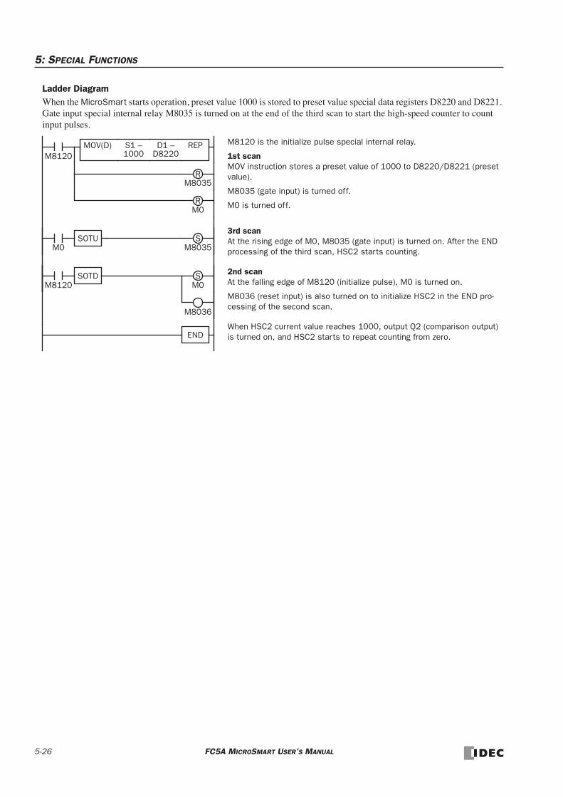
5: SPECIAL FUNCTIONS
Ladder DiagramWhen the MicroSmart starts operation, preset value 1000 is stored to preset value special data registers D8220 and D8221. Gate input special internal relay M8035 is turned on at the end of the third scan to start the high-speed counter to count input pulses.
M8120
M8120 is the initialize pulse special internal relay.
1st scan MOV instruction stores a preset value of 1000 to D8220/D8221 (preset value).
M8035 (gate input) is turned off.
M0 is turned off.
3rd scan At the rising edge of M0, M8035 (gate input) is turned on. After the END processing of the third scan, HSC2 starts counting.
2nd scan At the falling edge of M8120 (initialize pulse), M0 is turned on.
M8036 (reset input) is also turned on to initialize HSC2 in the END pro-cessing of the second scan.
When HSC2 current value reaches 1000, output Q2 (comparison output) is turned on, and HSC2 starts to repeat counting from zero.END
M0
M8035R
M8035SSOTU
M0R
M8120 M0SSOTD
REPS1 –1000
D1 –D8220
MOV(D)
M8036
5-26 FC5A MICROSMART USER’S MANUAL
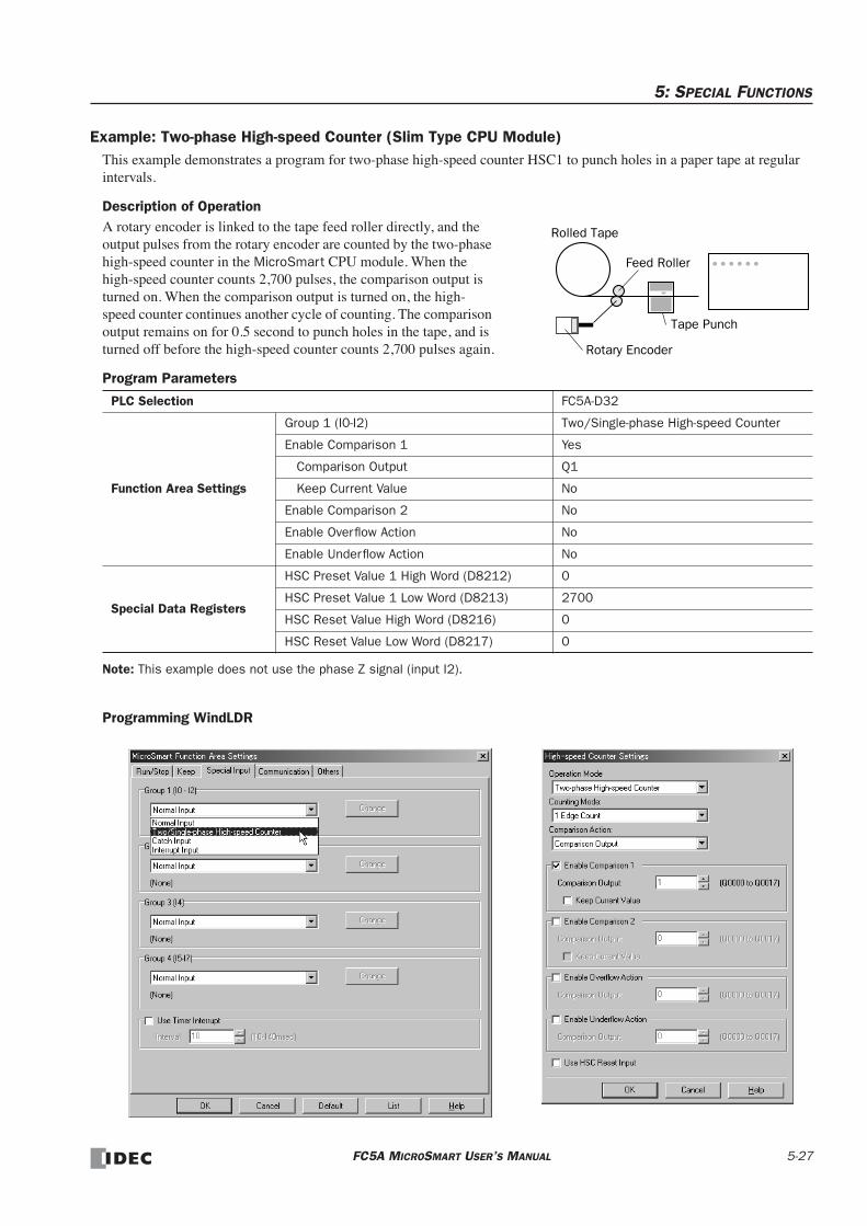
5: SPECIAL FUNCTIONS
Example: Two-phase High-speed Counter (Slim Type CPU Module)This example demonstrates a program for two-phase high-speed counter HSC1 to punch holes in a paper tape at regular intervals.
Description of OperationA rotary encoder is linked to the tape feed roller directly, and the output pulses from the rotary encoder are counted by the two-phase high-speed counter in the MicroSmart CPU module. When the high-speed counter counts 2,700 pulses, the comparison output is turned on. When the comparison output is turned on, the high-speed counter continues another cycle of counting. The comparison output remains on for 0.5 second to punch holes in the tape, and is turned off before the high-speed counter counts 2,700 pulses again.
Program Parameters
Note: This example does not use the phase Z signal (input I2).
Programming WindLDR
PLC Selection FC5A-D32
Function Area Settings
Group 1 (I0-I2) Two/Single-phase High-speed Counter
Enable Comparison 1 Yes
Comparison Output Q1
Keep Current Value No
Enable Comparison 2 No
Enable Overflow Action No
Enable Underflow Action No
Special Data Registers
HSC Preset Value 1 High Word (D8212) 0
HSC Preset Value 1 Low Word (D8213) 2700
HSC Reset Value High Word (D8216) 0
HSC Reset Value Low Word (D8217) 0
Feed Roller
Rotary Encoder
Tape Punch
Rolled Tape
FC5A MICROSMART USER’S MANUAL 5-27
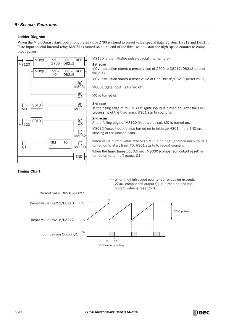
5: SPECIAL FUNCTIONS
Ladder DiagramWhen the MicroSmart starts operation, preset value 2700 is stored to preset value special data registers D8212 and D8213. Gate input special internal relay M8031 is turned on at the end of the third scan to start the high-speed counter to count input pulses.
Timing Chart
M8120
M8120 is the initialize pulse special internal relay.
1st scan MOV instruction stores a preset value of 2700 to D8212/D8213 (preset value 1).
MOV instruction stores a reset value of 0 to D8216/D8217 (reset value).
M8031 (gate input) is turned off.
M0 is turned off.
3rd scan At the rising edge of M0, M8031 (gate input) is turned on. After the END processing of the third scan, HSC1 starts counting.
2nd scan At the falling edge of M8120 (initialize pulse), M0 is turned on.
M8032 (reset input) is also turned on to initialize HSC1 in the END pro-cessing of the second scan.
When HSC1 current value reaches 2700, output Q1 (comparison output) is turned on to start timer T0. HSC1 starts to repeat counting.
When the timer times out 0.5 sec, M8030 (comparison output reset) is turned on to turn off output Q1.END
M0
M8031R
M8031SSOTU
REPD1 –D8212
S1 –2700
MOV(D)
REPD1 –D8216
S1 –0
MOV(D)
M0R
M8120 M0SSOTD
Q1TIM5
T0M8030
M8032
Comparison Output Q1ON
OFF
Current Value D8210/D8211
When the high-speed counter current value exceeds 2700, comparison output Q1 is turned on and the current value is reset to 0.
Reset Value D8216/D8217 0
2700
0.5 sec for punching
2700 pulses
Preset Value D8212/D8213
5-28 FC5A MICROSMART USER’S MANUAL

5: SPECIAL FUNCTIONS
Frequency MeasurementThe pulse frequency of input signals to input terminals I1, I3, I4, and I5 (all-in-one) or I7 (slim) can be counted using the high-speed counter function. The high-speed counter counts input pulses within a given period, calculates input pulse fre-quency, and stores the result to a special data register.
The all-in-one type CPU modules and slim type CPU modules have different frequency measurement configurations.
Frequency Measurement Operands for All-in-One Type CPU Modules
Frequency Measurement Operands for Slim Type CPU Modules
Precautions for Using Frequency Measurement Function• High-speed counters cannot be used for the group in which frequency measurement is used.
• While the gate input is on, the input pulse frequency is measured. To restart frequency measurement, turn off and on the gate input, or stop and run the CPU module.
• Before downloading a user program to the CPU module, turn off the gate input. If a user program is downloaded while the gate input is on, frequency measurement stops.
• Before the measured results are stored in the special data registers, it takes a maximum of calculation period plus one scan time. Using the FRQRF (frequency measurement refresh) instruction in the ladder diagram, the latest value of the fre-quency measurement can be read out within 250 ms regardless of the input frequency. For the FRQRF instruction, see page 18-10.
• For wiring the frequency measurement input signals, use a twisted-pair shielded cable.
DescriptionHigh-speed Counter No.
HSC1 HSC2 HSC3 HSC4
Input Terminal I1 I3 I4 I5
Gate Input M8031 M8035 M8041 M8045
Frequency Measurement Value D8060 D8062 D8064 D8066
Frequency Measurement Range 4 Hz to 50 kHz 4 Hz to 5 kHz
Measurement Error4 Hz to 4 kHz: ±10% maximum 4 kHz and above: ±0.1% maximum
Calculation PeriodBelow 4 kHz: 1 sec maximum 4 kHz and above: 250 ms maximum
DescriptionHigh-speed Counter No.
HSC1 HSC2 HSC3 HSC4
Input Terminal I1 I3 I4 I7
Gate Input M8031 M8035 M8041 M8045
Frequency Measurement ValueHigh Word D8060 D8062 D8064 D8066
Low Word D8061 D8063 D8065 D8067
Frequency Measurement Range 4 Hz to 100 kHz
Measurement Error4 Hz to 4 kHz: ±10% maximum 4 kHz and above: ±0.1% maximum
Calculation PeriodBelow 4 kHz: 1 sec maximum 4 kHz and above: 250 ms maximum
FC5A MICROSMART USER’S MANUAL 5-29

5: SPECIAL FUNCTIONS
Programming WindLDR (All-in-One Type CPU Modules)
1. From the WindLDR menu bar, select Configure > Function Area Settings. The Function Area Settings dialog box appears.
2. Select the Special Input tab.
3. When using frequency measurement, select Single-phase High-speed Counter in the Groups 1 through 4 pull-down list boxes.
Do not make other changes.
5-30 FC5A MICROSMART USER’S MANUAL

5: SPECIAL FUNCTIONS
Catch InputThe catch input function is used to receive short pulses from sensor outputs regardless of the scan time. Input pulses shorter than one scan time can be received. Four inputs I2 through I5 can be designated to catch a rising or falling edge of short input pulses, and the catch input statuses are stored to special internal relays M8154 through M8157, respectively. The Function Area Settings dialog box is used to designate inputs I2 through I5 as a catch input.
Normal input signals to input terminals are read when the END instruction is executed at the end of a scan.
Since these settings relate to the user program, the user program must be downloaded to the MicroSmart after changing any of these settings.
Catch Input Specifications
Note: Input filter settings have no effect on the catch inputs. For the input filter function, see page 5-37.
Catch Input Terminals and Special Internal Relays for Catch Inputs
Programming WindLDR
1. From the WindLDR menu bar, select Configure > Function Area Settings. The Function Area Settings dialog box appears.
2. Select the Special Input tab.
3. Select Catch Input in the Groups 1 through 4 pull-down list boxes. The Catch Input dialog box appears.
4. Select Catch Input Rising Edge or Catch Input Falling Edge in the pull-down list.
Minimum Turn ON Pulse Width All-in-one type: 40 µs Slim type: 5 µs
Minimum Turn OFF Pulse Width All-in-one type: 150 µs Slim type: 5 µs
Group Catch Input No. Special Internal Relay for Catch Input
Group 1 I2 M8154
Group 2 I3 M8155
Group 3 I4 M8156
Group 4 I5 M8157
Note: For wiring the catch input signals, use a twisted-pair shielded cable.
Catch Input Rising/Falling Edge SelectionCatch Input Rising Edge Catch Input Falling Edge
FC5A MICROSMART USER’S MANUAL 5-31

5: SPECIAL FUNCTIONS
Catching Rising Edge of Input Pulse
Catching Falling Edge of Input Pulse
Note: When two or more pulses enter within one scan, subsequent pulses are ignored.
Example: Maintaining Catch InputWhen a catch input is received, the catch input relay assigned to a catch input is turned on for only one scan. This example demonstrates a program to maintain a catch input status for more than one scan.
Actual Input ONOFF
Catch Input Relay ONOFF(M8154-M8157)
Note
ENDProcessed
1 scan time
(I2 to I5)
Actual Input ONOFF
Catch Input Relay ONOFF(M8154-M8157)
Note
ENDProcessed
(I2 to I5)
1 scan time
M0
M8154
Input I2 is designated as a catch input using the Function Area Settings.
When input I2 is turned on, special internal relay M8154 is turned on, and M0 is maintained in the self-holding circuit.
When NC input I1 is turned off, the self-holding circuit is unlatched, and M0 is turned off.
M0 is used as an input condition for the subsequent program instructions.
M0
I1 M0
5-32 FC5A MICROSMART USER’S MANUAL

5: SPECIAL FUNCTIONS
Interrupt InputAll MicroSmart CPU modules have an interrupt input function. When a quick response to an external input is required, such as positioning control, the interrupt input can call a subroutine to execute an interrupt program.
Four inputs I2 through I5 can be designated to execute interrupt at a rising and/or falling edge of input pulses. When an interrupt is initiated by inputs I2 through I5, program execution immediately jumps to a predetermined label number stored in special data registers D8032 through D8035, respectively. The Function Area Settings dialog box is used to des-ignate inputs I2 through I5 as an interrupt input, normal input, high-speed counter input, or catch input.
Normal input signals to input terminals are read when the END instruction is executed at the end of a scan.
Since these settings relate to the user program, the user program must be downloaded to the MicroSmart after changing any of these settings.
Interrupt Input Terminals, Special Data Registers, and Special Internal Relays for Interrupt Inputs
Programming WindLDR
1. From the WindLDR menu bar, select Configure > Function Area Settings. The Function Area Settings dialog box appears.
2. Select the Special Input tab.
3. Select Interrupt Input in the Groups 1 through 4 pull-down list boxes. the Interrupt Input dialog box appears.
4. Select an interrupt edge in the pull-down list for each group.
Disable and Enable InterruptsThe interrupt inputs I2 through I5 and timer interrupt are normally enabled while the CPU is running, and can also be indi-vidually disabled using the DI instruction or enabled using the EI instruction. When interrupt inputs I2 through I5 are enabled, special internal relay M8140 through M8143 are turned on, respectively. See page 18-5.
Group Interrupt Input No. Interrupt Input Jump Destination Label No. Interrupt Input Status
Group 1 I2 D8032 M8140
Group 2 I3 D8033 M8141
Group 3 I4 D8034 M8142
Group 4 I5 D8035 M8143
Interrupt Input Rising/Falling Edge Selection
Interrupt at Rising Edge Interrupt occurs when the interrupt input turns on.
Interrupt at Falling Edge Interrupt occurs when the interrupt input turns off.
Interrupt at Both Edges Interrupt occurs when the interrupt input turns on or off.
FC5A MICROSMART USER’S MANUAL 5-33

5: SPECIAL FUNCTIONS
Example: Interrupt InputThe following example demonstrates a program of using the interrupt input function, with input I2 designated as an inter-rupt input. When the interrupt input is turned on, the input I0 status is immediately transferred to output Q0 using the IOREF (I/O refresh) instruction before the END instruction is executed. For the IOREF instruction, see page 18-7.
Notes for Using Interrupt Inputs and Timer Interrupt:• When using an interrupt input or timer interrupt, separate the interrupt program from the main program using the END
instruction at the end of the main program.
• When an interrupt program calls another subroutine, a maximum of 3 subroutine calls can be nested. If more than 3 calls are nested, a user program execution error occurs, turning on special internal relay M8004 and the ERR LED.
• When using an interrupt input or timer interrupt, include the label number of the interrupt program to be executed when an interrupt occurs. The label numbers stored in data registers D8032 through D8036 specify the interrupt programs for interrupt inputs I2 through I5 and timer interrupt, respectively.
• When more than one interrupt input is turned on at the same time, interrupt program execution is given priority to inputs I2, I3, I4, and I5, in that order. If an interrupt is initiated while another interrupt program is executed, the subsequent inter-rupt program is executed after the prior interrupt is completed. Multiple interrupt programs cannot be executed simulta-neously.
• Make sure that the execution time of the interrupt program is shorter than interrupt intervals sufficiently.
• Interrupt programs cannot use the following instructions: SOTU, SOTD, TML, TIM, TMH, TMS, CNT, CDP, CUD, SFR, SFRN, WKTIM, WKTBL, DISP, DGRD, TXD1/2, RXD1/2, DI, EI, XYFS, CVXTY, CVYTX, PULS1/2/3, PWM1/2/3, RAMP1/2, ZRN1/2/3, PID, DTML, DTIM, DTMH, DTMS, TTIM, RUNA, and STPA.
• For wiring the interrupt input signals, use a twisted-pair shielded cable.
M8120 is the initialize pulse special internal relay.
D8032 stores 0 to designate jump destination label 0 for interrupt input I2.
The interrupt program is separated from the main program by the END instruction.
When input I2 is on, program execution jumps to label 0.
M8125 is the in-operation output special internal relay.
IOREF immediately reads input I0 status to internal relay M300.
M300 turns on or off the output Q0 internal memory.
Another IOREF immediately writes the output Q0 internal memory status to actual output Q0.
Program execution returns to the main program.
Insert LRET at the end of the subroutine to return to the main program.
LABEL0
M8120
END
Main Program
M8125
Q0
REPS1 –0
D1 –D8032
MOV(W)
IOREF S1I0
M300
M8125IOREF S1
Q0
LRET
5-34 FC5A MICROSMART USER’S MANUAL

5: SPECIAL FUNCTIONS
Timer InterruptIn addition to the interrupt input as described in the preceding section, all CPU modules have a timer interrupt function. When a repetitive operation is required, the timer interrupt can be used to call a subroutine repeatedly at predetermined intervals of 10 through 140 ms.
The Function Area Settings dialog box is used to enable the timer interrupt and to specify the interval, from 10 to 140 ms, to execute the timer interrupt. When the timer interrupt is enabled, the program execution jumps to the jump destination label number stored in special data register D8036 repeatedly while the CPU is running. When the interrupt program is completed, the program execution returns to the main program at the address where the interrupt occurred.
Since these settings relate to the user program, the user program must be downloaded to the CPU module after changing any of these settings.
Special Data Register and Special Internal Relay for Timer Interrupt
Programming WindLDR
1. From the WindLDR menu bar, select Configure > Function Area Settings. The Function Area Settings dialog box appears.
2. Select the Special Input tab.
3. Click the check box on the left of Timer Interrupt to use the timer interrupt function.
4. Select an interval to execute the timer interrupt, from 10 to 140 ms.
Disable and Enable InterruptsThe timer interrupt and interrupt inputs I2 through I5 are normally enabled while the CPU is running, and can also be indi-vidually disabled using the DI instruction or enabled using the EI instruction. When timer interrupt is enabled, M8144 is turned on. When disabled, M8144 is turned off. See page 18-5.
InterruptSpecial Data Register for Timer Interrupt
Jump Destination Label No.Special Internal Relay for
Timer Interrupt Status
Timer Interrupt D8036 M8144
FC5A MICROSMART USER’S MANUAL 5-35

5: SPECIAL FUNCTIONS
Example: Timer InterruptThe following example demonstrates a program of using the timer interrupt function. The Function Area Settings must also be completed to use the timer interrupt function as described on the preceding page.
Notes for Using Timer Interrupt and Interrupt Inputs:• When using a timer interrupt or interrupt input, separate the interrupt program from the main program using the END
instruction at the end of the main program.
• When an interrupt program calls another subroutine, a maximum of 3 subroutine calls can be nested. If more than 3 calls are nested, a user program execution error occurs, turning on special internal relay M8004 and the ERR LED.
• When using a timer interrupt or interrupt input, include the label number of the interrupt program to be executed when an interrupt occurs. The label numbers stored in data registers D8032 through D8036 specify the interrupt programs for interrupt inputs I2 through I5 and timer interrupt, respectively.
• If an interrupt is initiated while another interrupt program is executed, the subsequent interrupt program is executed after the prior interrupt is completed. Multiple interrupt programs cannot be executed simultaneously.
• Make sure that the execution time of the interrupt program is shorter than interrupt intervals sufficiently.
• Interrupt programs cannot use the following instructions: SOTU, SOTD, TML, TIM, TMH, TMS, CNT, CDP, CUD, SFR, SFRN, WKTIM, WKTBL, DISP, DGRD, TXD1/2, RXD1/2, DI, EI, XYFS, CVXTY, CVYTX, PULS1/2/3, PWM1/2/3, RAMP1/2, ZRN1/2/3, PID, DTML, DTIM, DTMH, DTMS, TTIM, RUNA, and STPA.
M8120 is the initialize pulse special internal relay.
D8036 stores 0 to designate jump destination label 0 for timer interrupt.
The interrupt program is separated from the main program by the END instruction.
While the CPU is running, program execution jumps to label 0 repeatedly at intervals selected in the Function Area Settings.
Each time the interrupt program is completed, program execution returns to the main program at the address where timer interrupt occurred.
Insert LRET at the end of the subroutine to return to the main program.
LABEL0
M8120
END
Main Program
REPS1 –0
D1 –D8036
MOV(W)
LRET
Interrupt Program
5-36 FC5A MICROSMART USER’S MANUAL

5: SPECIAL FUNCTIONS
Input FilterThe input filter function is used to reject input noises. The catch input function described in the preceding section is used to read short input pulses to special internal relays. On the contrary, the input filter rejects short input pulses when the MicroSmart is used with input signals containing noises.
Different input filter values can be selected for inputs I0 through I7 in four groups using the Function Area Settings. Selectable input filter values to pass input signals are 0 ms, and 3 through 15 ms in 1-ms increments. Default value is 3 ms for all inputs I0 through I7. Inputs I10 and above on 16- and 24-I/O all-in-one type CPU modules and 32-I/O slim type CPU modules are provided with a fixed filter of 3 ms. Inputs I30 and above on all expansion input modules have a fixed fil-ter of 4 ms. The input filter rejects inputs shorter than the selected input filter value minus 2 ms.
Normal inputs require a pulse width of the filter value plus one scan time to receive input signals. When using the input fil-ter function, select Normal Input on the Special Input page in the Function Area Settings.
Since these settings relate to the user program, the user program must be downloaded to the MicroSmart after changing any of these settings.
Programming WindLDR
1. From the WindLDR menu bar, select Configure > Function Area Settings. The Function Area Settings dialog box appears.
2. Select the Others tab.
3. Select an input filter value for each group of inputs.
Input Filter Values and Input OperationDepending on the selected values, the input filter has three response areas to reject or pass input signals.
Reject area: Input signals do not pass the filter (selected filter value minus 2 ms). Indefinite area: Input signals may be rejected or passed. Pass area: Input signals pass the filter (selected filter value).
Example: Input Filter 8 msTo reject input pulses of 6 ms or less, select input filter value of 8 ms. Then input pulses of 8 ms plus one scan time are accepted correctly at the END processing.
Input Filter GroupGroup 1: I0Group 2: I1Group 3: I2, I3Group 4: I4 - I7
Input Filter Time Selection0 ms, 3 through 15 ms in 1-ms incrementsDefault: 3 ms
Indefinite
6 ms 8 ms + 1 scan
Rejected AcceptedInput
FC5A MICROSMART USER’S MANUAL 5-37

5: SPECIAL FUNCTIONS
User Program ProtectionThe user program in the MicroSmart CPU module can be protected from reading, writing, or both using the Function Area Settings in WindLDR.
Programming WindLDR
1. From the WindLDR menu bar, select Configure > Function Area Settings. The Function Area Settings dialog box appears.
2. Select the Others tab.
3. Under Protect User Program, select a required protect mode in the pull-down list.
Unprotected: The user program in the CPU module can be read and written without a password. Write Protected: Prevents inadvertent replacement of the user program. Read Protected: Prevents unauthorized copying of the user program. Read/Write Protected: Protects the user program from reading and writing.
4. When a required protect mode is selected, the Password Setting dialog box appears.
Enter a password of 1 through 8 ASCII characters from the key board in the Password field, and enter the same pass-word in the Confirm Password field.
5. Click the OK button and download the user program to the MicroSmart after changing any of these settings.
• Before proceeding with the following steps, make sure to note the protect code, which is needed to disable the user program protection. If the user program in the MicroSmart CPU module is write- or read/write-protected, the user program cannot be changed without the protect code.
Warning
5-38 FC5A MICROSMART USER’S MANUAL

5: SPECIAL FUNCTIONS
Disabling ProtectionWhen the user program is protected against read and/or write, the protection can be temporarily disabled using WindLDR.
1. From the WindLDR menu bar, select Online > Monitor. The monitor mode is enabled.
2. From the WindLDR menu bar, select Online > PLC Status. The PLC Status dialog box appears.
3. Under the Protect Status in the PLC Status dialog box, click the Disable button. The Disable Protect dialog box appears.
4. Enter the password, and click the OK button.
The user program protection is disabled temporarily, and reading is allowed once.
Enabling ProtectionWhen the CPU module is powered up again, the protection designated in the user program takes effect again.
For read or read/write protect, once the user program is uploaded, the protection automatically takes effect again. For write protect, the protection designated in the newly downloaded user program takes effect.
To change the protection permanently, change the protection settings and download the user program.
FC5A MICROSMART USER’S MANUAL 5-39

5: SPECIAL FUNCTIONS
Constant Scan TimeThe scan time may vary whether basic and advanced instructions are executed or not depending on input conditions to these instructions. The scan time can be made constant by entering a required scan time preset value into special data reg-ister D8022 reserved for constant scan time. When performing accurate repetitive control, make the scan time constant using this function. The constant scan time preset value can be between 1 and 1,000 ms.
The scan time error is ±1 ms of the preset value normally. When the data link or other communication functions are used, the scan time error may be increased to several milliseconds.
When the actual scan time is longer than the scan time preset value, the scan time cannot be reduced to the constant value.
Special Data Registers for Scan TimeIn addition to D8022, three more special data registers are reserved to indicate current, maximum, and minimum scan time values.
Example: Constant Scan TimeThis example sets the scan time to a constant value of 500 ms.
D8022 Constant Scan Time Preset Value (1 to 1,000 ms)
D8023 Scan Time Current Value (ms)
D8024 Scan Time Maximum Value (ms)
D8025 Scan Time Minimum Value (ms)
M8120REP
M8120 is the initialize pulse special internal relay.
When the CPU starts operation, the MOV (move) instruction stores 500 to special data register D8022.
The scan time is set to a constant value of 500 ms.
S1 –500
D1 –D8022
MOV(W)
5-40 FC5A MICROSMART USER’S MANUAL

5: SPECIAL FUNCTIONS
Online Edit, Run-Time Program Download, and Test Program DownloadNormally, the CPU module has to be stopped before downloading a user program. Using WindLDR 5.0, the FC5A Micro-Smart CPU modules have online edit capabilities which allow to make small modifications to the user program while monitoring the CPU module operation on the WindLDR screen either in the 1:1 or 1:N computer link system.
While monitoring on the WindLDR screen, the modified user program can be downloaded in two ways: run-time program download and test program download.
When executing run-time program download, the modified user program is downloaded to the EEPROM in the CPU mod-ule and replaces the original user program permanently. When download is completed, the modified program is executed and monitored on the WindLDR screen.
The test program download replaces the user program in the RAM only and does not overwrite the EEPROM immediately. When test program download is completed, the modified program is executed while the original user program still remain in the EEPROM. Before quitting the test program download, you are asked whether to store the modified user program in the EEPEOM or discard the modified program.
Before performing the online edit, a user program has to be downloaded to the CPU module using the ordinary program download. Add or delete a part of the same user program, or make small changes to the same user program, and download the modified user program using the run-time program download or test program download while the CPU is running to confirm the changes online.
Another method of using this feature is: upload the user program from the CPU module to WindLDR, make changes, and download the modified user program while the CPU is running.
FC5A MICROSMART USER’S MANUAL 5-41

5: SPECIAL FUNCTIONS
Online EditBefore starting the online edit using WindLDR, download a user program to the CPU module or upload a user program from the CPU module using the ordinary program download or upload. If user programs do not match between WindLDR and the CPU module, the online edit cannot be used.
Online edit can not change Function Area Settings and Expansion Data Register values. Only ladder diagrams can be edited.
When TIM/CNT preset values have been changed as a result of advanced instructions or through communication, confirm or clear the changes before starting the online edit. See page 7-13.
If you do not want to clear the new preset values during the run-time program download or test program download, you can import the new preset values to the user program. Access the PLC Status dialog box from the Online menu in the mon-itoring mode. Then click the Confirm button in the TIM/CNT Change Status field. (The displayed status will switch from Changed to Unchanged.) Upload the user program, which has new preset values in place of the original preset values. Make changes to the uploaded user program, then perform the run-time program download or test program download. Note that the Confirm button has effect on both timer and counter preset values.
Note: When “Enable D10000 to D49999” has been selected in the Function Area Settings for the slim type CPU module, the online edit cannot be used. To use the online edit, deselect the use of extra data registers D10000 to D49999. See page 6-2.
Programming WindLDR
1. From the WindLDR menu bar, select Online > Online Edit while the CPU module is running.
WindLDR enters Online Edit mode where the user program can be modified while monitoring the CPU module operation.
2. Edit the user program.
In this example, a rung is inserted, two NC contacts are programmed in series and connected to an output.
The added program is monitored immediately.
5-42 FC5A MICROSMART USER’S MANUAL

5: SPECIAL FUNCTIONS
Run-Time Program Download
The run-time program download function is used to download a modified user program to the EEPROM in the CPU mod-ule while the CPU is running. When program download is complete, the CPU module executes the new program in the next scan.
When run-time program download is completed, outputs, internal relays, shift registers, timer/counter current values, and data registers maintain the previous statuses. Timer/counter preset values are replaced by the new values.
Programming WindLDR
1. To execute run-time program download, select Online > Run-Time Program Download.
The Download Program Dialog appears.
2. Click the Download button to start downloading the user program to the EEPROM in the CPU module.
• The run-time program download may cause unexpected operation of the MicroSmart. Before start-ing the run-time program download, make sure of safety after understanding the function correctly.
• If many changes are made to a user program, the possibility of unexpected operation increases. Keep changes to a minimum in one modification and download the user program to make sure of safety.
• If a user program syntax error or user program writing error occurs during the run-time program download, the CPU module is stopped and all outputs are turned off, which may cause hazards depending on the application.
• Immediately when program download is completed, the new user program is executed. It takes a maximum of 60 seconds to store the downloaded program to the EEPROM. In this period, the scan time is extended by about 10 to 130 ms per scan.
• While executing the run-time program download, do not shut down the CPU module or disconnect the communication cable. Otherwise, a fatal error may occur such as user program writing error, which may cause hazards depending on the application.
• When executing the run-time program download, output statuses are maintained. When an OUT/OUTN instruction is deleted or an output operand number has been changed, the output status is maintained after executing the run-time program download. This may cause hazards depending on the application.
Caution
FC5A MICROSMART USER’S MANUAL 5-43

5: SPECIAL FUNCTIONS
3. Monitor the downloaded program.
4. To quit the online edit mode, select Online > Online Edit.
Notes for Using Run-Time Program Download:• When DISP, DGRD, AVRG, PULS, PWM, RAMP, ZRN, or PID instructions have been added or edited, the input to these
instructions needs to remain off for one scan time to initialize these inputs.
• SOTU/SOTD instructions are initialized in the first scan after the run-time program download is completed.
• Function Area Settings and Expansion Data Register values cannot be changed using the online edit. To change these set-tings, download the user program using the ordinary program download procedure.
• When the communication buffer for TXD/RXD instructions still holds the instruction data, the run-time program download does not overwrite the data in the communication buffer immediately. After the communication has been completed according to the existing data in the buffer, the new data for TXD/RXD instructions takes effect. To clear the receive buffer for the RXD instruction, turn on the special internal relay for user communication receive instruction cancel flag, such as M8022 for port 1 or M8023 for port 2. See the example on page 5-47.
• If communication is interrupted during run-time program download, disparity between user programs in the RAM and EEPROM occurs. If this is the case, quit the online edit and download the user program to the CPU module using the ordi-nary program download procedure.
5-44 FC5A MICROSMART USER’S MANUAL

5: SPECIAL FUNCTIONS
Test Program Download
The test program download replaces the user program in the RAM only and does not overwrite the EEPROM immediately. When test program download is completed, the modified program is executed while the original user program still remains in the EEPROM. Before quitting the test program download, you are asked whether to store the modified user program to the EEPEOM or discard the modified program.
When test program download is completed, outputs, internal relays, shift registers, timer/counter current values, and data registers maintain the previous statuses. Timer/counter preset values are replaced by the new values.
Programming WindLDR
1. To execute test program download, select Debug > Download Test Program.
The Download Program Dialog appears.
2. Click the Download button to start downloading the user program to the RAM in the CPU module.
• The test program download may cause unexpected operation of the MicroSmart. Before starting the test program download, make sure of safety after understanding the function correctly.
• If many changes are made to a user program, the possibility of unexpected operation increases. Keep changes to a minimum in one modification and download the user program to make sure of safety.
• If a user program syntax error or user program writing error occurs during the test program down-load, the CPU module is stopped and all outputs are turned off, which may cause hazards depending on the application.
• Before quitting the test program download, confirm or cancel the test program to select whether to store the modified user program to the EEPROM or discard the changes. Before executing the con-firming procedure, the EEPROM stores the original user program. If the CPU module is shut down before confirming, the modified user program is lost.
• When cancelling the test program after making changes to the user program, only the original user program is restored and operand values are not restored.
• While executing the test program download, do not shut down the CPU module or disconnect the communication cable. Otherwise, a fatal error may occur such as user program writing error, which may cause hazards depending on the application.
• When executing the test program download, output statuses are maintained. When an OUT/OUTN instruction is deleted or an output operand number has been changed, the output status is maintained after executing the test program download. This may cause hazards depending on the application.
• When executing the Cancel Test Program, the original user program in the EEPROM is restored, but operand values are maintained and are not restored.
Caution
FC5A MICROSMART USER’S MANUAL 5-45

5: SPECIAL FUNCTIONS
3. Monitor the downloaded program.
Before quitting the test program download, you have to store the modified user program to the EEPEOM or discard the modified program.
4-1. To store the downloaded program to the EEPROM, select Debug > Confirm Test Program (RAM to EEPROM). When a confirmation box appears, click Yes to store the downloaded program to the EEPROM.
The modified program is stored from the RAM to the EEPROM and can still be monitored.
4-2. To discard the downloaded program, select Debug > Cancel Test Program. When a confirmation box appears, click Yes to discard the downloaded program
The original user program stored in the EEPROM is restored and loaded to the RAM.
5. To quit the online edit mode, select Online > Online Edit.
5-46 FC5A MICROSMART USER’S MANUAL

5: SPECIAL FUNCTIONS
Notes for Using Test Program Download:• Immediately when test program download is complete, the new user program is executed.
• When executing the Confirm Test Program, it takes a maximum of 60 seconds to store the downloaded program to the EEPROM. In this period, the scan time is extended by about 10 to 130 ms per scan.
• When the Download Test Program (to RAM) or Cancel Test Program is completed, special internal relay M8126 turns on for one scan time.
• When DISP, DGRD, AVRG, PULS, PWM, RAMP, ZRN, or PID instructions have been added or edited, the input to these instructions needs to remain off for one scan time to initialize these inputs.
• SOTU/SOTD instructions are initialized in the first scan after the Download Test Program (to RAM) or Cancel Test Program is completed.
• Function Area Settings and Expansion Data Register values cannot be changed using the online edit. To change these set-tings, download the user program using the ordinary program download procedure.
• When the communication buffer for TXD/RXD instructions still holds the instruction data, the Download Test Program (to RAM) or Cancel Test Program operation does not overwrite the data in the communication buffer immediately. After the communication has been completed according to the existing data in the buffer, the new data for TXD/RXD instructions takes effect. To clear the receive buffer for the RXD instruction, turn on the special internal relay for user communication receive instruction cancel flag, such as M8022 for port 1 or M8023 for port 2. See the example on page 5-47.
• If communication is interrupted during test program download, disparity between user programs in the RAM and EEPROM occurs. If this is the case, quit the online edit and download the user program to the CPU module using the ordinary pro-gram download procedure.
M8126 Run-Time Program Download Completion (ON for 1 scan)After the run-time program download has been completed, special internal relay M8126 turns on for one scan time when the CPU starts to run. During the test program download, M8126 also turns on for one scan time when the Download Test Program (to RAM) or Cancel Test Program is completed. This special internal relay is useful for initializing instructions.
Example: Initialize the AVRG instruction after Run-Time Program Download
Example: Cancel all RXD instructions after Run-Time Program Download
Even if M0 is on, the AVRG instruction is initial-ized when the run-time program download is completed.M0
S1D0
S2M0
AVRG(W) D2M100
S3D100
D1D200M8126
When the run-time program download is completed, special internal relay M8022 (user communication receive instruction cancel flag for port 1) is turned on to cancel all RXD1 instructions.M8126 M8022
FC5A MICROSMART USER’S MANUAL 5-47

5: SPECIAL FUNCTIONS
Analog PotentiometersThe all-in-one 10- and 16-I/O type CPU modules and every slim type CPU module have one analog potentiometer. Only the 24-I/O type CPU module has two analog potentiometers. The values (0 through 255) set with analog potentiometers 1 and 2 are stored to data registers D8057 and D8058, respectively, and updated in every scan.
The analog potentiometer can be used to change the preset value for a timer or counter.
Special Data Registers for Analog Potentiometers
Example: Changing Counter Preset Value Using Analog PotentiometerThis example demonstrates a program to change a counter preset value using analog potentiometer 1.
CPU Module Analog Potentiometer 1 Analog Potentiometer 2
FC5A-C24R2 and FC5A-C24R2C D8057 D8058
Other CPU Modules D8057 —
Analog Potentiometer 1
Analog Potentiometer 2(24-I/O Type Only)
All-in-One Type CPU Module
Slim Type CPU Module
Analog Potentiometer 1
CNT C0D8057
I1
Reset
PulseI0
Analog potentiometer 1 value is stored to data register D8057, which is used as a preset value for counter C0.
The preset value is changed between 0 and 255 using the potentiometer.
5-48 FC5A MICROSMART USER’S MANUAL

5: SPECIAL FUNCTIONS
Analog Voltage InputEvery slim type CPU module has an analog voltage input connector. When an analog voltage of 0 through 10V DC is applied to the analog voltage input connector, the signal is converted to a digital value of 0 through 255 and stored to spe-cial data register D8058. The data is updated in every scan.
Special Data Register for Analog Voltage Input
To connect an external analog source, use the attached cable.
The cable is also available optionally.
CPU Module Analog Voltage Input Data
Slim Type CPU Modules D8058
Cable Name Type No.
Analog Voltage Input Cable(1m/3.28 ft. long)
FC4A-PMAC2P (package quantity 2)
• Do not apply a voltage exceeding 10V DC to the analog voltage input, otherwise the CPU module may be damaged.
+ (red)
– (black)
Analog Voltage Source(0 to 10V DC)
Caution
FC5A MICROSMART USER’S MANUAL 5-49

5: SPECIAL FUNCTIONS
HMI ModuleThis section describes the functions and operation of the optional HMI module (FC4A-PH1). The HMI module can be installed on any all-in-one type CPU module, and also on the HMI base module mounted next to any slim type CPU mod-ule. The HMI module makes it possible to manipulate the RAM data in the CPU module without using the Online menu options in WindLDR. For details about the specifications of the HMI module, see page 2-66.
HMI module functions include:
• Displaying timer/counter current values and changing timer/counter preset values
• Displaying and changing data register values
• Setting and resetting bit operand statuses, such as inputs, outputs, internal relays, and shift register bits
• Displaying and clearing error data
• Starting and stopping the PLC
• Displaying and changing calendar/clock data (only when using the clock cartridge)
• Confirming changed timer/counter preset values
Parts Description
• Power up the MicroSmart CPU module after installing the HMI module. If the HMI module is installed or removed while the MicroSmart is powered up, the HMI module may fail to operate cor-rectly.
• If an invalid operand or a value over 65535 is entered, the display screen flashes to signal an error. When an error screen displays, press the ESC button and repeat the correct key operation.
ESC ButtonCancels the current operation, and returns to the immediately
preceding operation.
ButtonScrolls up the menu, or increments the
selected operand number or value.
ButtonScrolls down the menu, or decrements the selected operand number or value.
OK ButtonGoes into each control screen, or enters the current operation.
Display ScreenThe liquid crystal display shows menus, operands, and data.
Caution
5-50 FC5A MICROSMART USER’S MANUAL

5: SPECIAL FUNCTIONS
Key Operation for Scrolling Menus after Power-upThe chart below shows the sequence of scrolling menus using the and buttons on the HMI module after power-up.
While a menu screen is shown, press the OK button to enter into each control screen where operand numbers and values are selected. For details of each operation, see the following pages.
Initial ScreenIndicates the PLC system program version or the same menu as when the PLC was powered down, depending on the value stored in special data register D8068 (see the next page).
Press the button to switch to the timer menu.
Timer MenuDisplays a timer current value, and changes the timer preset value.
Counter MenuDisplays a counter current value, and changes the counter preset value.
Data Register Menu (D0XXXX)Displays and changes the data regis-ter value of D0 and above.
Data Register Menu (D1XXXX)Displays and changes the data regis-ter value of D10000 and above.
Data Register Menu (D2XXXX)Displays and changes the data regis-ter value of D20000 and above.
Data Register Menu (D3XXXX)Displays and changes the data regis-ter value of D30000 and above.
Data Register Menu (D4XXXX)Displays and changes the data regis-ter value of D40000 and above.
Input MenuDisplays an input status, and sets/ resets the input.
Output MenuDisplays an output status, and sets/ resets the output.
Internal Relay MenuDisplays an internal relay status, and sets or resets the internal relay.
Shift Register MenuDisplays a shift register bit status, and sets/resets the shift register bit.
Error MenuDisplays general error codes, and clears the general error codes.
Run/Stop MenuDisplays the run/stop status of the PLC, and starts or stops the PLC.
Calendar MenuDisplays and changes the calendar data.
Clock MenuDisplays and changes the clock data.
Timer/Counter Changed Preset Value Confirm MenuConfirms changed timer/counter pre-set values. (The changed preset values in the MicroSmart CPU module RAM are written to EEPROM.)
FC5A MICROSMART USER’S MANUAL 5-51

5: SPECIAL FUNCTIONS
Special Internal Relays for HMI ModuleTwo special internal relays are provided protect the HMI operation.
Selection of HMI Module Initial ScreenD8068 can be used to select the initial screen display of the HMI module when the CPU module is powered up.
When a keep data error occurs, mode 1 is enabled regardless of the value stored in data register D8068.
Key Operation for Selecting Operand NumberWhen the OK button is pressed while a menu screen is shown, the screen switches to the control screen of the menu. For example, while the timer menu is on the display, pressing the OK button switches the screen to the timer control screen, where operand numbers and values are selected. For operation examples, see the following pages.
Internal Relay Name Description
M8011 HMI Write Prohibit FlagWhen M8011 is turned on, the HMI module is disabled from writing data to prevent unauthorized modifications, such as direct set/reset, changing timer/counter preset values, and entering data into data registers.
M8012 HMI Operation Prohibit FlagWhen M8012 is turned on, the HMI module is disabled from all opera-tions, reducing the scan time. To turn off M8012, power down and up the CPU, or use the Point Write on WindLDR.
Data Register Value Description
D80680, 2 through 65535 Mode 1: Indicates the PLC program version each time the PLC is powered up.
1 Mode 2: Indicates the same menu as when the PLC was shut down.
OK Switches to the control screen.
Slow Flashing
ESC Discards the changes and returns to the menu screen.
Shifts up one digit.
Decrements the number.
Shifts down one digit.
Increments the number.
OK Saves the changes and goes to the next screen.
Fast Flashing
OK Selects the digit and changes to fast flashing.ESC Returns to slow flashing.
ESC Returns to fast flashing.
Timer Menu
5-52 FC5A MICROSMART USER’S MANUAL

5: SPECIAL FUNCTIONS
Displaying Timer/Counter Current Values and Changing Timer/Counter Preset ValuesThis section describes the procedure for displaying a timer current value and for changing the timer preset value for an example. The same procedure applies to counter current values and preset values.
Example: Change timer T28 preset value 820 to 900
1. Select the Timer menu.
2. Select the operand number.
3. The current value of the selected timer number is displayed.
4. The preset value of the selected timer number is displayed. Change the preset value to 900 as described below.
5. The changed preset value is displayed without flashing.
Note: The changed timer/counter preset values are stored in the MicroSmart CPU module RAM and backed up for 30 days by a lithium backup battery. If required, the changed preset values can be written from the MicroSmart CPU module RAM to the EEPROM using the Timer/Counter Changed Preset Value Confirm menu described on page 5-54. For the data movement in the CPU module, see page 7-13.
OK
Go to control screen.
OK
Slow Flash
Select digit.
Quick Flash
Decrement the value.
ESC
Back to digit selection.
Shift up one digit.
Quick Flash Slow Flash
OK
Slow Flash
Select digit.
Quick Flash
Increment the value.
OK
Complete operand selection.Go to next screen.
Quick Flash
OK
Go to next screen.
Current Value
Slow Flash
Shift up one digit.
OK
Slow Flash
Select digit.
ESC
Decrement the value.
Back to digit selection.
Quick Flash Quick Flash
Slow Flash
Shift up one digit.
OK
Slow Flash
Select digit.
OK
Increment the value.
Save the changes.
Quick Flash Quick Flash
OK
Return to the Timer menu.
New Preset Value
FC5A MICROSMART USER’S MANUAL 5-53

5: SPECIAL FUNCTIONS
Example: When timer T28 preset value is designated using a data registerNote: Data registers designated as timer/counter preset values are displayed only for all-in-one CPU modules.
1. Select the Timer menu.
2. Select the operand number.
3. The current value of the selected timer number is displayed.
4. The data register number designated as a preset value is displayed.
Confirming Changed Timer/Counter Preset ValuesThis section describes the procedure for writing changed timer/counter preset values from the MicroSmart CPU module RAM to the EEPROM. This operation writes the changed preset values of both timers and counters at once.
The changed timer/counter preset values are stored in the MicroSmart CPU module RAM and backed up for 30 days by a lithium backup battery. If required, the changed preset values can be written to the MicroSmart CPU module EEPROM as described below. For the data movement in the CPU module, see page 7-13.
1. Select the Timer/Counter Changed Preset Value Confirm menu.
2. Confirm the changed timer/counter preset values, and write the changes from the RAM to the EEPROM.
OK
Go to control screen.
OK
Slow Flash
Select digit.
Quick Flash
Decrement the value.
ESC
Back to digit selection.
Shift up one digit.
Quick Flash Slow Flash
OK
Slow Flash
Select digit.
Quick Flash
Increment the value.
OK
Complete operand selection.Go to next screen.
Quick Flash
OK
Go to next screen.On slim type CPU modules, the screen does not change any more.To return to the Timer menu, press the ESC button.
Current Value
ESC
Data Register No.
When the preset value is designated using a data register, the data register number is displayed, and the screen does not change any more. To return to the Timer menu, press the ESC button.
OK
Display the TIM/CNT change status.
TIM/CNT change status0: Unchanged 1: Changed
The Timer/Counter Changed Preset Value Confirm menu is restored.To abort confirming the changed timer/counter preset values, press the ESC button instead of the OK button; the Timer/Counter Changed Preset Value Confirm menu is restored.
OK
Confirm the changed TIM/CNT preset values.
5-54 FC5A MICROSMART USER’S MANUAL

5: SPECIAL FUNCTIONS
Displaying and Changing Data Register ValuesThis section describes the procedure for displaying and changing the data register value.
Data register menus DR0, DR1, DR2, DR3, and DR4 determine the 10,000’s place of the data register number to display and change values.
Note: When “Enable D10000 to D49999” has been selected in the Function Area Settings, and data register menu DR1, DR2, DR3, or DR4 is selected, then the data register value can be displayed and changed.
Example: Change data register D180 value to 1300
1. Select the Data Register menu DR0.
2. Select the operand number.
3. The data of the selected data register number is displayed.
4. Change the data to 1300 as described below.
5. The changed data is displayed without flashing.
OK
Go to control screen.
Slow Flash
Shift up one digit.
OK
Slow Flash
Select digit.
ESC
Decrement the value.
Back to digit selection.
Quick Flash Quick Flash
Slow Flash
Shift up one digit.
OK
Slow Flash
Select digit.
Increment the value
Quick Flash
OK
Complete operand selection.
Quick Flash
OK
Go to next screen.
Current Data
Slow Flash
Shift up two digits.
OK
Slow Flash
Select digit.
ESC
Increment the value.
Back to digit selection.
Quick Flash Quick Flash
Slow Flash
Shift up one digit.
OK
Slow Flash
Select digit.
OK
Increment the value.
Save the changes.
Quick Flash Quick Flash
OK
Return to the Data Register menu.
New Data
FC5A MICROSMART USER’S MANUAL 5-55

5: SPECIAL FUNCTIONS
Setting and Resetting Bit Operand StatusBit operand statuses, such as inputs, outputs, internal relays, and shift register bits, can be displayed, and set or reset using the MHI module.
This section describes the procedure for displaying an internal relay status and for setting the internal relay for an example. The same procedure applies to inputs, outputs, and shift register bits.
Example: Set internal relay M120
1. Select the Internal Relay menu.
2. Select the operand number.
3. The status of the selected internal relay number is displayed.
4. Select 1 (set) or 0 (reset) using the or button.
5. The changed status is displayed without flashing.
OK
Go to control screen.
Slow Flash
Shift up one digit.
OK
Slow Flash
Select digit.
ESC
Increment the value.
Back to digit selection.
Quick Flash Quick Flash
Slow Flash
Shift up one digit.
OK
Slow Flash
Select digit.
Increment the value.
Quick Flash
OK
Complete operand selection.
Quick Flash
OK
Current Status
Internal relay status0: OFF 1: ON
Quick Flash
Increment the value.0: Reset (OFF) 1: Set (ON)
OK
Enable the change.
Quick Flash
OK
Return to the Internal Relay menu.
New Status
5-56 FC5A MICROSMART USER’S MANUAL
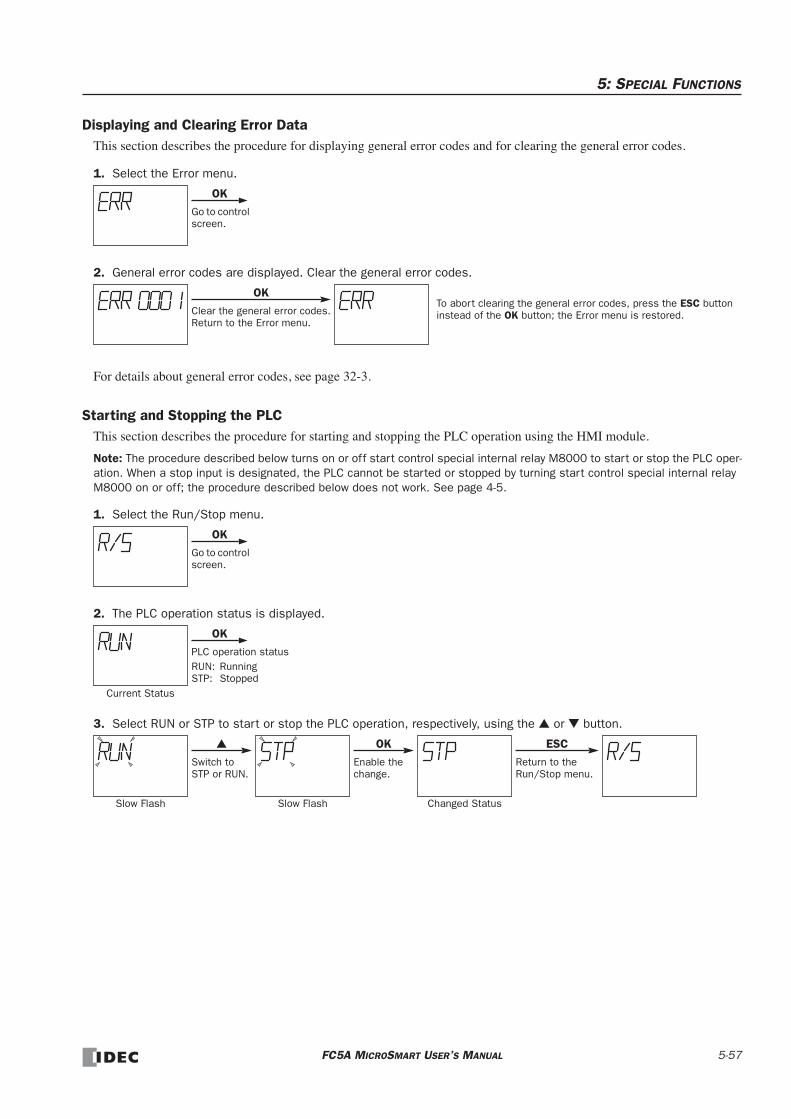
5: SPECIAL FUNCTIONS
Displaying and Clearing Error DataThis section describes the procedure for displaying general error codes and for clearing the general error codes.
1. Select the Error menu.
2. General error codes are displayed. Clear the general error codes.
For details about general error codes, see page 32-3.
Starting and Stopping the PLCThis section describes the procedure for starting and stopping the PLC operation using the HMI module.
Note: The procedure described below turns on or off start control special internal relay M8000 to start or stop the PLC oper-ation. When a stop input is designated, the PLC cannot be started or stopped by turning start control special internal relay M8000 on or off; the procedure described below does not work. See page 4-5.
1. Select the Run/Stop menu.
2. The PLC operation status is displayed.
3. Select RUN or STP to start or stop the PLC operation, respectively, using the or button.
OK
Go to control screen.
OK
Clear the general error codes. Return to the Error menu.
To abort clearing the general error codes, press the ESC button instead of the OK button; the Error menu is restored.
OK
Go to control screen.
OK
Current Status
PLC operation statusRUN: Running STP: Stopped
Slow Flash
Switch to STP or RUN.
OK
Slow Flash
Enable the change.
ESC
Return to the Run/Stop menu.
Changed Status
FC5A MICROSMART USER’S MANUAL 5-57

5: SPECIAL FUNCTIONS
Displaying and Changing Calendar Data (only when using the clock cartridge)When an optional clock cartridge (FC4A-PT1) is installed in the MicroSmart CPU module, the calendar data of the clock cartridge can be displayed and changed using the HMI module as described in this section.
Example: Change calendar data from Saturday, 01/01/2000 to Wednesday, 04/04/2001
1. Select the Calendar menu.
2. The calendar data is displayed.
3. Change the year data using the or button.
4. Change the month data using the or button.
5. Change the day data using the or button.
6. Change the day of week data using the or button.
7. The new calendar data is displayed without flashing.
OK
Go to control screen.
OK
Current Data
Slow Flash
Increment the value.
OK
Slow Flash
Enable the change.
Slow Flash
Increment the value.
OK
Slow Flash
Enable the change.
Slow Flash
Increment the value.
OK
Slow Flash
Enable the change.
Slow Flash
Decrement the value.
OK
Slow Flash
Enable the change.
ESC
New Data
Return to the Calendar menu.
5-58 FC5A MICROSMART USER’S MANUAL

5: SPECIAL FUNCTIONS
Displaying and Changing Clock Data (only when using the clock cartridge)When an optional clock cartridge (FC4A-PT1) is installed in the MicroSmart CPU module, the clock data of the clock car-tridge can be displayed and changed using the HMI module as described in this section.
Example: Change clock data from 12:05 to 10:10
1. Select the Clock menu.
2. The clock data is displayed.
3. Change the hour data using the or button.
4. Change the minute data using the or button.
5. The new clock data is displayed without flashing.
OK
Go to control screen.
OK
Current Data
Slow Flash
Decrement the value.
OK
Slow Flash
Enable the change.
Slow Flash
Increment the value.
OK
Slow Flash
Enable the change.
ESC
New Data
Return to the Clock menu.
FC5A MICROSMART USER’S MANUAL 5-59

5: SPECIAL FUNCTIONS
5-60 FC5A MICROSMART USER’S MANUAL

6: ALLOCATION NUMBERS
IntroductionThis chapter describes allocation numbers available for the MicroSmart to program basic and advanced instructions. Spe-cial internal relays and special data registers are also described.
The MicroSmart is programmed using operands such as inputs, outputs, internal relays, timers, counters, shift registers, and data registers.
Inputs (I) are relays to receive input signals through the input terminals. Outputs (Q) are relays to send the processed results of the user program to the output terminals. Internal relays (M) are relays used in the CPU and cannot be outputted to the output terminals. Special internal relays (M) are internal relays dedicated to specific functions. Timers (T) are relays used in the user program, available in 1-sec, 100-ms, 10-ms, and 1-ms timers. Counters (C) are relays used in the user program, available in adding counters and reversible counters. Shift registers (R) are registers to shift the data bits according to pulse inputs. Data registers (D) are registers used to store numerical data. Some of the data registers are dedicated to special functions.
Operand Allocation NumbersAvailable I/O numbers depend on the type of the MicroSmart CPU module and the combination of I/O modules. I/O mod-ules can be used with only the 24-I/O type CPU module among all-in-one type CPU modules. All slim type CPU modules can be used with I/O modules to expand the I/O points. For details of I/O, internal relay, and special internal relay num-bers, see page 6-3.
All-in-One Type CPU Modules
Notes:• The least significant digit of input, output, internal relay, and special internal relay operand number is an octal number (0
through 7). Upper digits are decimal numbers.
• The allocation numbers of expansion inputs and outputs start with I30 and Q30, respectively.
• Note that input and output allocation numbers are not continuous between the CPU module and expansion I/O modules.
• The 24-I/O type CPU module (FC5A-C24R2) can add a maximum of 64 I/O points, and use a maximum of 88 points of inputs and outputs in total.
OperandFC5A-C10R2 FC5A-C10R2C
FC5A-C16R2 FC5A-C16R2C
FC5A-C24R2 FC5A-C24R2C
Allocation No. Points Allocation No. Points Allocation No. Points
Input (I) I0 - I5 6I0 - I7I10
9I0 - I7I10 - I15
14 78 total
Expansion Input (I) — — — — I30 - I107 64
Output (Q) Q0 - Q3 4 Q0 - Q6 7Q0 - Q7Q10 - Q11
10 74 total
Expansion Output (Q) — — — — Q30 - Q107 64
Internal Relay (M) M0 - M2557 2048 M0 - M2557 2048 M0 - M2557 2048
Special Internal Relay (M)
M8000 - M8157 128 M8000 - M8157 128 M8000 - M8157 128
Shift Register (R) R0 - R127 128 R0 - R127 128 R0 - R127 128
Timer (T) T0 - T255 256 T0 - T255 256 T0 - T255 256
Counter (C) C0 - C255 256 C0 - C255 256 C0 - C255 256
Data Register (D) D0 - D1999 2000 D0 - D1999 2000 D0 - D1999 2000
Special Data Register (D)
D8000 - D8199 200 D8000 - D8199 200 D8000 - D8199 200
FC5A MICROSMART USER’S MANUAL 6-1

6: ALLOCATION NUMBERS
Slim Type CPU Modules
Notes:• The least significant digit of input, output, internal relay, and special internal relay operand number is an octal number (0
through 7). Upper digits are decimal numbers.
• The allocation numbers of expansion inputs and outputs start with I30 and Q30, respectively.
• Note that input and output allocation numbers are not continuous between the CPU module and expansion I/O modules.
• A maximum of 7 expansion I/O modules can be mounted on all slim type CPU modules. The maximum I/O points depend on the CPU module type as described below.
• The 16-I/O relay output type CPU module (FC5A-D16RK1 and FC5A-D16RS1) can add a maximum of 480 I/O points, and use a maximum of 496 points of inputs and outputs in total. When more than 224 I/O points are expanded, the expansion interface module is needed.
• The 32-I/O type CPU module (FC5A-D32K3 and FC5A-D32S3) can add a maximum of 480 I/O points, and use a maximum of 512 points of inputs and outputs in total. When more than 224 I/O points are expanded, the expansion interface module is needed.
• Extra data registers D10000 through D49999 can be enabled by designating in WindLDR. From the WindLDR menu bar, select Configure > Function Area Settings > Others > Extra Data Registers.
OperandFC5A-D16RK1FC5A-D16RS1
FC5A-D32K3FC5A-D32S3
Allocation No. Points Allocation No. Points
Input (I) I0 - I7 8488 total
I0 - I7I10 - I17
16496 total
Expansion Input (I) I30 - I627 480 I30 - I627 480
Output (Q) Q0 - Q7 8488 total
Q0 - Q7Q10 - Q17
16496 total
Expansion Output (Q) Q30 - Q627 480 Q30 - Q627 480
Internal Relay (M) M0 - M2557 2,048 M0 - M2557 2,048
Special Internal Relay (M) M8000 - M8317 256 M8000 - M8317 256
Shift Register (R) R0 - R255 256 R0 - R255 256
Timer (T) T0 - T255 256 T0 - T255 256
Counter (C) C0 - C255 256 C0 - C255 256
Data Register (D) D0 - D1999 2,000 D0 - D1999 2,000
Expansion Data Register (D) D2000 - D7999 6,000 D2000 - D7999 6,000
Special Data Register (D) D8000 - D8499 500 D8000 - D8499 500
Extra Data Register (D) D10000 - D49999 40,000 D10000 - D49999 40,000
6-2 FC5A MICROSMART USER’S MANUAL

6: ALLOCATION NUMBERS
I/O, Internal Relay, and Special Internal Relay Operand Allocation Numbers
Operand Allocation Numbers CPU Module
Input (I)
I0-I5 FC5A-C10R2
I0-I7 I10 FC5A-C16R2
I0-I7 I10-I15I30-I37 I40-I47 I50-I57 I60-I67 I70-I77 I80-I87 I90-I97 I100-I107
FC5A-C24R2
I0-I7 I30-I37 I40-I47 I50-I57 I60-I67 I70-I77 I80-I87 I90-I97 I100-I107 I110-I117 I120-I127 I130-I137 I140-I147 I150-I157 I160-I167 I170-I177 I180-I187 I190-I197 I200-I207 I210-I217 I220-I227 I230-I237 I240-I247 I250-I257 I260-I267 I270-I277 I280-I287 I290-I297 I300-I307 I310-I317 I320-I327 I330-I337 I340-I347 I350-I357 I360-I367 I370-I377 I380-I387 I390-I397 I400-I407 I410-I417 I420-I427 I430-I437 I440-I447 I450-I457 I460-I467 I470-I477 I480-I487 I490-I497 I500-I507 I510-I517 I520-I527 I530-I537 I540-I547 I550-I557 I560-I567 I570-I577 I580-I587 I590-I597 I600-I607 I610-I617 I620-I627
FC5A-D16RK1FC5A-D16RS1
I0-I7 I10-I17I30-I37 I40-I47 I50-I57 I60-I67 I70-I77 I80-I87 I90-I97 I100-I107 I110-I117 I120-I127 I130-I137 I140-I147 I150-I157 I160-I167 I170-I177 I180-I187 I190-I197 I200-I207 I210-I217 I220-I227 I230-I237 I240-I247 I250-I257 I260-I267 I270-I277 I280-I287 I290-I297 I300-I307 I310-I317 I320-I327 I330-I337 I340-I347 I350-I357 I360-I367 I370-I377 I380-I387 I390-I397 I400-I407 I410-I417 I420-I427 I430-I437 I440-I447 I450-I457 I460-I467 I470-I477 I480-I487 I490-I497 I500-I507 I510-I517 I520-I527 I530-I537 I540-I547 I550-I557 I560-I567 I570-I577 I580-I587 I590-I597 I600-I607 I610-I617 I620-I627
FC5A-D32K3FC5A-D32S3
Output (Q)
Q0-Q3 FC5A-C10R2
Q0-Q6 FC5A-C16R2
Q0-Q7 Q10-Q11Q30-Q37 Q40-Q47 Q50-Q57 Q60-Q67 Q70-Q77 Q80-Q87 Q90-Q97 Q100-Q107
FC5A-C24R2
Q0-Q7Q30-Q37 Q40-Q47 Q50-Q57 Q60-Q67 Q70-Q77 Q80-Q87 Q90-Q97 Q100-Q107 Q110-Q117 Q120-Q127 Q130-Q137 Q140-Q147 Q150-Q157 Q160-Q167 Q170-Q177 Q180-Q187 Q190-Q197 Q200-Q207 Q210-Q217 Q220-Q227 Q230-Q237 Q240-Q247 Q250-Q257 Q260-Q267 Q270-Q277 Q280-Q287 Q290-Q297 Q300-Q307 Q310-Q317 Q320-Q327 Q330-Q337 Q340-Q347 Q350-Q357 Q360-Q367 Q370-Q377 Q380-Q387 Q390-Q397 Q400-Q407 Q410-Q417 Q420-Q427 Q430-Q437 Q440-Q447 Q450-Q457 Q460-Q467 Q470-Q477 Q480-Q487 Q490-Q497 Q500-Q507 Q510-Q517 Q520-Q527 Q530-Q537 Q540-Q547 Q550-Q557 Q560-Q567 Q570-Q577 Q580-Q587 Q590-Q597 Q600-Q607 Q610-Q617 Q620-Q627
FC5A-D16RK1FC5A-D16RS1
FC5A MICROSMART USER’S MANUAL 6-3
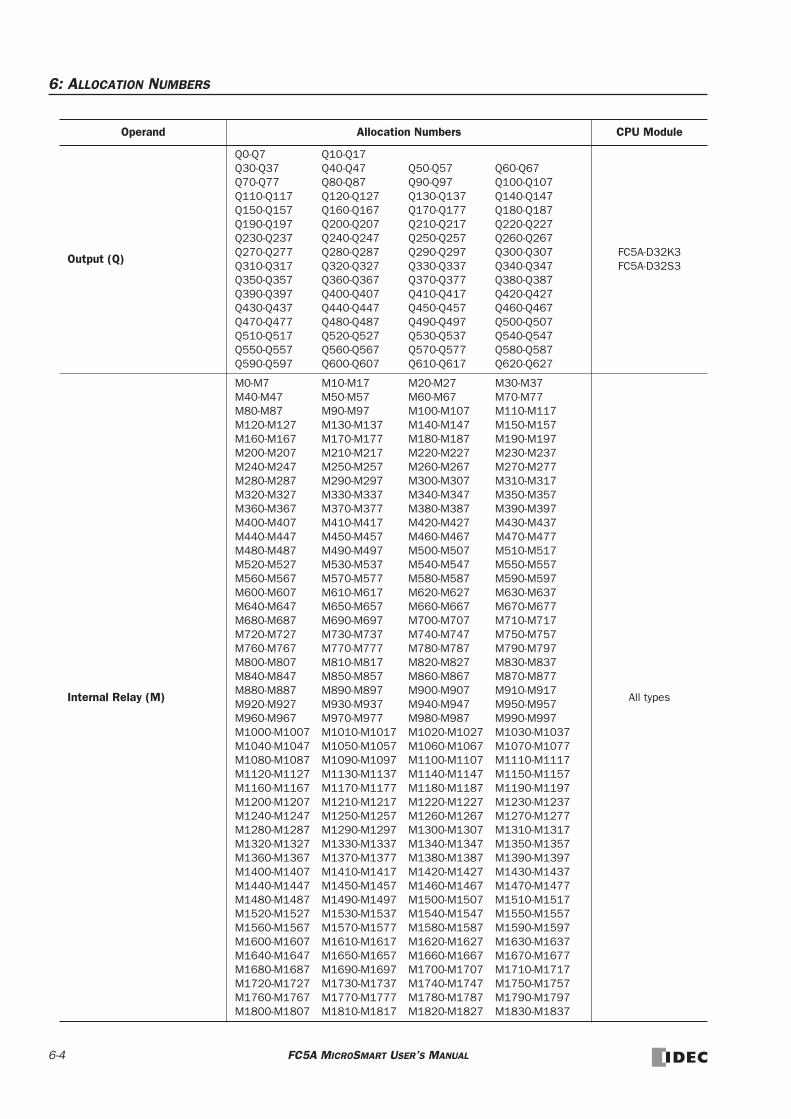
6: ALLOCATION NUMBERS
Output (Q)
Q0-Q7 Q10-Q17Q30-Q37 Q40-Q47 Q50-Q57 Q60-Q67 Q70-Q77 Q80-Q87 Q90-Q97 Q100-Q107 Q110-Q117 Q120-Q127 Q130-Q137 Q140-Q147 Q150-Q157 Q160-Q167 Q170-Q177 Q180-Q187 Q190-Q197 Q200-Q207 Q210-Q217 Q220-Q227 Q230-Q237 Q240-Q247 Q250-Q257 Q260-Q267 Q270-Q277 Q280-Q287 Q290-Q297 Q300-Q307 Q310-Q317 Q320-Q327 Q330-Q337 Q340-Q347 Q350-Q357 Q360-Q367 Q370-Q377 Q380-Q387 Q390-Q397 Q400-Q407 Q410-Q417 Q420-Q427 Q430-Q437 Q440-Q447 Q450-Q457 Q460-Q467 Q470-Q477 Q480-Q487 Q490-Q497 Q500-Q507 Q510-Q517 Q520-Q527 Q530-Q537 Q540-Q547 Q550-Q557 Q560-Q567 Q570-Q577 Q580-Q587 Q590-Q597 Q600-Q607 Q610-Q617 Q620-Q627
FC5A-D32K3FC5A-D32S3
Internal Relay (M)
M0-M7 M10-M17 M20-M27 M30-M37M40-M47 M50-M57 M60-M67 M70-M77M80-M87 M90-M97 M100-M107 M110-M117M120-M127 M130-M137 M140-M147 M150-M157M160-M167 M170-M177 M180-M187 M190-M197M200-M207 M210-M217 M220-M227 M230-M237M240-M247 M250-M257 M260-M267 M270-M277M280-M287 M290-M297 M300-M307 M310-M317M320-M327 M330-M337 M340-M347 M350-M357M360-M367 M370-M377 M380-M387 M390-M397M400-M407 M410-M417 M420-M427 M430-M437M440-M447 M450-M457 M460-M467 M470-M477M480-M487 M490-M497 M500-M507 M510-M517M520-M527 M530-M537 M540-M547 M550-M557M560-M567 M570-M577 M580-M587 M590-M597M600-M607 M610-M617 M620-M627 M630-M637M640-M647 M650-M657 M660-M667 M670-M677M680-M687 M690-M697 M700-M707 M710-M717M720-M727 M730-M737 M740-M747 M750-M757M760-M767 M770-M777 M780-M787 M790-M797M800-M807 M810-M817 M820-M827 M830-M837M840-M847 M850-M857 M860-M867 M870-M877M880-M887 M890-M897 M900-M907 M910-M917M920-M927 M930-M937 M940-M947 M950-M957M960-M967 M970-M977 M980-M987 M990-M997M1000-M1007 M1010-M1017 M1020-M1027 M1030-M1037M1040-M1047 M1050-M1057 M1060-M1067 M1070-M1077M1080-M1087 M1090-M1097 M1100-M1107 M1110-M1117M1120-M1127 M1130-M1137 M1140-M1147 M1150-M1157M1160-M1167 M1170-M1177 M1180-M1187 M1190-M1197M1200-M1207 M1210-M1217 M1220-M1227 M1230-M1237M1240-M1247 M1250-M1257 M1260-M1267 M1270-M1277M1280-M1287 M1290-M1297 M1300-M1307 M1310-M1317M1320-M1327 M1330-M1337 M1340-M1347 M1350-M1357M1360-M1367 M1370-M1377 M1380-M1387 M1390-M1397M1400-M1407 M1410-M1417 M1420-M1427 M1430-M1437M1440-M1447 M1450-M1457 M1460-M1467 M1470-M1477M1480-M1487 M1490-M1497 M1500-M1507 M1510-M1517M1520-M1527 M1530-M1537 M1540-M1547 M1550-M1557M1560-M1567 M1570-M1577 M1580-M1587 M1590-M1597M1600-M1607 M1610-M1617 M1620-M1627 M1630-M1637M1640-M1647 M1650-M1657 M1660-M1667 M1670-M1677M1680-M1687 M1690-M1697 M1700-M1707 M1710-M1717M1720-M1727 M1730-M1737 M1740-M1747 M1750-M1757M1760-M1767 M1770-M1777 M1780-M1787 M1790-M1797M1800-M1807 M1810-M1817 M1820-M1827 M1830-M1837
All types
Operand Allocation Numbers CPU Module
6-4 FC5A MICROSMART USER’S MANUAL

6: ALLOCATION NUMBERS
Internal Relay (M)
M1840-M1847 M1850-M1857 M1860-M1867 M1870-M1877M1880-M1887 M1890-M1897 M1900-M1907 M1910-M1917M1920-M1927 M1930-M1937 M1940-M1947 M1950-M1957M1960-M1967 M1970-M1977 M1980-M1987 M1990-M1997M2000-M2007 M2010-M2017 M2020-M2027 M2030-M2037M2040-M2047 M2050-M2057 M2060-M2067 M2070-M2077M2080-M2087 M2090-M2097 M2100-M2107 M2110-M2117M2120-M2127 M2130-M2137 M2140-M2147 M2150-M2157M2160-M2167 M2170-M2177 M2180-M2187 M2190-M2197M2200-M2207 M2210-M2217 M2220-M2227 M2230-M2237M2240-M2247 M2250-M2257 M2260-M2267 M2270-M2277M2280-M2287 M2290-M2297 M2300-M2307 M2310-M2317M2320-M2327 M2330-M2337 M2340-M2347 M2350-M2357M2360-M2367 M2370-M2377 M2380-M2387 M2390-M2397M2400-M2407 M2410-M2417 M2420-M2427 M2430-M2437M2440-M2447 M2450-M2457 M2460-M2467 M2470-M2477M2480-M2487 M2490-M2497 M2500-M2507 M2510-M2517M2520-M2527 M2530-M2537 M2540-M2547 M2550-M2557
All types
Special Internal Relay (M)
M8000-M8007 M8010-M8017 M8020-M8027 M8030-M8037M8040-M8047 M8050-M8057 M8060-M8067 M8070-M8077M8080-M8087 M8090-M8097 M8100-M8107 M8110-M8117M8120-M8127 M8130-M8137 M8140-M8147 M8150-M8157
FC5A-C10R2FC5A-C16R2FC5A-C24R2
M8000-M8007 M8010-M8017 M8020-M8027 M8030-M8037M8040-M8047 M8050-M8057 M8060-M8067 M8070-M8077M8080-M8087 M8090-M8097 M8100-M8107 M8110-M8117M8120-M8127 M8130-M8137 M8140-M8147 M8150-M8157M8160-M8167 M8170-M8177 M8180-M8187 M8190-M8197M8200-M8207 M8210-M8217 M8220-M8227 M8230-M8237M8240-M8247 M8250-M8257 M8260-M8267 M8270-M8277M8280-M8287 M8290-M8297 M8300-M8307 M8310-M8317
FC5A-D16RK1FC5A-D16RS1FC5A-D32K3FC5A-D32S3
Operand Allocation Numbers CPU Module
FC5A MICROSMART USER’S MANUAL 6-5

6: ALLOCATION NUMBERS
Operand Allocation Numbers for END Refresh Type Analog I/O Modules
Note: Each analog I/O module uses 20 data registers. When analog modules are not connected, the corresponding data registers can be used as ordinary data registers.
Operand Allocation Numbers for AS-Interface Master Module 1
Note: AS-Interface master module 1 uses internal relays and data registers shown above. When AS-Interface master module is not connected, these internal relays and data registers can be used as ordinary data registers. When two AS-Interface modules are used, operands are allocated to AS-Interface master module 2 using the RUNA instruction.
Analog I/O Module Number Analog Input Channel 0 Analog Input Channel 1 Analog Output Reserved
1 D760-D765 D766-D771 D772-D777 D778, D779
2 D780-D785 D786-D791 D792-D797 D798, D799
3 D800-D805 D806-D811 D812-D817 D818, D819
4 D820-D825 D826-D831 D832-D837 D838, D839
5 D840-D845 D846-D851 D852-D857 D858, D859
6 D860-D865 D866-D871 D872-D877 D878, D879
7 D880-D885 D886-D891 D892-D897 D898, D899
MicroSmart CPU Module 1 AS-Interface Master Module EEPROM
Operand Allocation No. AS-Interface Object
AS-Interface Internal Relays
M1300-M1617 Digital input (IDI)
M1620-M1937 Digital output (ODI)
M1940-M1997 Status information
AS-Interface Data Registers
D1700-D1731 Analog input
D1732-D1763 Analog output
D1764-D1767 List of active slaves (LAS)
D1768-D1771 List of detected slaves (LDS)
D1772-D1775 List of peripheral fault slaves (LPF)
D1776-D1779 List of projected slaves (LPS)
D1780-D1811 Configuration data image A (CDI)
D1812-D1843 Configuration data image B (CDI)
D1844-D1875 Permanent configuration data A (PCD)
D1876-D1907 Permanent configuration data B (PCD)
D1908-D1923 Parameter image (PI)
D1924-D1939 Permanent parameter (PP)
D1940 Slave 0 ID1 code
D1941-D1945 For ASI command description
D1946-D1999 — Reserved —
6-6 FC5A MICROSMART USER’S MANUAL

6: ALLOCATION NUMBERS
Operand Allocation Numbers for Data Link Master Station
Note: When any slave stations are not connected, master station data registers which are assigned to the vacant slave sta-tions can be used as ordinary data registers.
Operand Allocation Numbers for Data Link Slave Station
Note: Slave station data registers D912 through D1271 and D8070 through D8099 can be used as ordinary data registers.
Slave Station NumberAllocation Number
Transmit Data to Slave Station
Receive Data from Slave Station
Data Link Communication Error
Slave Station 1 D900-D905 D906-D911 D8069
Slave Station 2 D912-D917 D918-D923 D8070
Slave Station 3 D924-D929 D930-D935 D8071
Slave Station 4 D936-D941 D942-D947 D8072
Slave Station 5 D948-D953 D954-D959 D8073
Slave Station 6 D960-D965 D966-D971 D8074
Slave Station 7 D972-D977 D978-D983 D8075
Slave Station 8 D984-D989 D990-D995 D8076
Slave Station 9 D996-D1001 D1002-D1007 D8077
Slave Station 10 D1008-D1013 D1014-D1019 D8078
Slave Station 11 D1020-D1025 D1026-D1031 D8079
Slave Station 12 D1032-D1037 D1038-D1043 D8080
Slave Station 13 D1044-D1049 D1050-D1055 D8081
Slave Station 14 D1056-D1061 D1062-D1067 D8082
Slave Station 15 D1068-D1073 D1074-D1079 D8083
Slave Station 16 D1080-D1085 D1086-D1091 D8084
Slave Station 17 D1092-D1097 D1098-D1103 D8085
Slave Station 18 D1104-D1109 D1110-D1115 D8086
Slave Station 19 D1116-D1121 D1122-D1127 D8087
Slave Station 20 D1128-D1133 D1134-D1139 D8088
Slave Station 21 D1140-D1145 D1146-D1151 D8089
Slave Station 22 D1152-D1157 D1158-D1163 D8090
Slave Station 23 D1164-D1169 D1170-D1175 D8091
Slave Station 24 D1176-D1181 D1182-D1187 D8092
Slave Station 25 D1188-D1193 D1194-D1199 D8093
Slave Station 26 D1200-D1205 D1206-D1211 D8094
Slave Station 27 D1212-D1217 D1218-D1223 D8095
Slave Station 28 D1224-D1229 D1230-D1235 D8096
Slave Station 29 D1236-D1241 D1242-D1247 D8097
Slave Station 30 D1248-D1253 D1254-D1259 D8098
Slave Station 31 D1260-D1265 D1266-D1271 D8099
DataAllocation Number
Transmit Data to Master Station
Receive Data from Master Station
Data Link Communication Error
Slave Station Data D900-D905 D906-D911 D8069
FC5A MICROSMART USER’S MANUAL 6-7
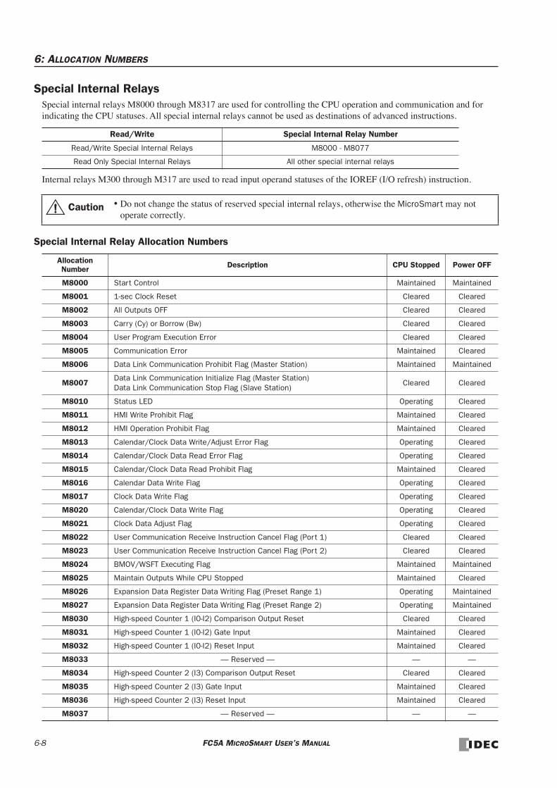
6: ALLOCATION NUMBERS
Special Internal RelaysSpecial internal relays M8000 through M8317 are used for controlling the CPU operation and communication and for indicating the CPU statuses. All special internal relays cannot be used as destinations of advanced instructions.
Internal relays M300 through M317 are used to read input operand statuses of the IOREF (I/O refresh) instruction.
Special Internal Relay Allocation Numbers
Read/Write Special Internal Relay Number
Read/Write Special Internal Relays M8000 - M8077
Read Only Special Internal Relays All other special internal relays
• Do not change the status of reserved special internal relays, otherwise the MicroSmart may not operate correctly.
Allocation Number Description CPU Stopped Power OFF
M8000 Start Control Maintained Maintained
M8001 1-sec Clock Reset Cleared Cleared
M8002 All Outputs OFF Cleared Cleared
M8003 Carry (Cy) or Borrow (Bw) Cleared Cleared
M8004 User Program Execution Error Cleared Cleared
M8005 Communication Error Maintained Cleared
M8006 Data Link Communication Prohibit Flag (Master Station) Maintained Maintained
M8007Data Link Communication Initialize Flag (Master Station) Data Link Communication Stop Flag (Slave Station)
Cleared Cleared
M8010 Status LED Operating Cleared
M8011 HMI Write Prohibit Flag Maintained Cleared
M8012 HMI Operation Prohibit Flag Maintained Cleared
M8013 Calendar/Clock Data Write/Adjust Error Flag Operating Cleared
M8014 Calendar/Clock Data Read Error Flag Operating Cleared
M8015 Calendar/Clock Data Read Prohibit Flag Maintained Cleared
M8016 Calendar Data Write Flag Operating Cleared
M8017 Clock Data Write Flag Operating Cleared
M8020 Calendar/Clock Data Write Flag Operating Cleared
M8021 Clock Data Adjust Flag Operating Cleared
M8022 User Communication Receive Instruction Cancel Flag (Port 1) Cleared Cleared
M8023 User Communication Receive Instruction Cancel Flag (Port 2) Cleared Cleared
M8024 BMOV/WSFT Executing Flag Maintained Maintained
M8025 Maintain Outputs While CPU Stopped Maintained Cleared
M8026 Expansion Data Register Data Writing Flag (Preset Range 1) Operating Maintained
M8027 Expansion Data Register Data Writing Flag (Preset Range 2) Operating Maintained
M8030 High-speed Counter 1 (I0-I2) Comparison Output Reset Cleared Cleared
M8031 High-speed Counter 1 (I0-I2) Gate Input Maintained Cleared
M8032 High-speed Counter 1 (I0-I2) Reset Input Maintained Cleared
M8033 — Reserved — — —
M8034 High-speed Counter 2 (I3) Comparison Output Reset Cleared Cleared
M8035 High-speed Counter 2 (I3) Gate Input Maintained Cleared
M8036 High-speed Counter 2 (I3) Reset Input Maintained Cleared
M8037 — Reserved — — —
Caution
6-8 FC5A MICROSMART USER’S MANUAL

6: ALLOCATION NUMBERS
M8040 High-speed Counter 3 (I4) Comparison Output Reset Cleared Cleared
M8041 High-speed Counter 3 (I4) Gate Input Maintained Cleared
M8042 High-speed Counter 3 (I4) Reset Input Maintained Cleared
M8043 — Reserved — — —
M8044 High-speed Counter 4 (I5-I7) Comparison Output Reset Cleared Cleared
M8045 High-speed Counter 4 (I5-I7) Gate Input Maintained Cleared
M8046 High-speed Counter 4 (I5-I7) Reset Input Maintained Cleared
M8047 — Reserved — — —
M8050 Modem Mode (Originate): Initialization String Star t Maintained Maintained
M8051 Modem Mode (Originate): ATZ Start Maintained Maintained
M8052 Modem Mode (Originate): Dialing Star t Maintained Maintained
M8053 Modem Mode (Disconnect): Disconnect Line Star t Maintained Maintained
M8054 Modem Mode (General Command): AT Command Start Maintained Maintained
M8055 Modem Mode (Answer): Initialization String Star t Maintained Maintained
M8056 Modem Mode (Answer): ATZ Start Maintained Maintained
M8057 Modem Mode AT Command Execution Maintained Cleared
M8060 Modem Mode (Originate): Initialization String Completion Maintained Cleared
M8061 Modem Mode (Originate): ATZ Completion Maintained Cleared
M8062 Modem Mode (Originate): Dialing Completion Maintained Cleared
M8063 Modem Mode (Disconnect): Disconnect Line Completion Maintained Cleared
M8064 Modem Mode (General Command): AT Command Completion Maintained Cleared
M8065 Modem Mode (Answer): Initialization String Completion Maintained Cleared
M8066 Modem Mode (Answer): ATZ Completion Maintained Cleared
M8067 Modem Mode Operational State Maintained Cleared
M8070 Modem Mode (Originate): Initialization String Failure Maintained Cleared
M8071 Modem Mode (Originate): ATZ Failure Maintained Cleared
M8072 Modem Mode (Originate): Dialing Failure Maintained Cleared
M8073 Modem Mode (Disconnect): Disconnect Line Failure Maintained Cleared
M8074 Modem Mode (General Command): AT Command Failure Maintained Cleared
M8075 Modem Mode (Answer): Initialization String Failure Maintained Cleared
M8076 Modem Mode (Answer): ATZ Failure Maintained Cleared
M8077 Modem Mode Line Connection Status Maintained Cleared
M8080Data Link Slave Station 1 Communication Completion Relay (Master Station) Data Link Communication Completion Relay (Slave Station) Modbus Communication Completion Relay (Modbus Master/Slave)
Operating Cleared
M8081 Data Link Slave Station 2 Communication Completion Relay Operating Cleared
M8082 Data Link Slave Station 3 Communication Completion Relay Operating Cleared
M8083 Data Link Slave Station 4 Communication Completion Relay Operating Cleared
M8084 Data Link Slave Station 5 Communication Completion Relay Operating Cleared
M8085 Data Link Slave Station 6 Communication Completion Relay Operating Cleared
M8086 Data Link Slave Station 7 Communication Completion Relay Operating Cleared
M8087 Data Link Slave Station 8 Communication Completion Relay Operating Cleared
M8090 Data Link Slave Station 9 Communication Completion Relay Operating Cleared
M8091 Data Link Slave Station 10 Communication Completion Relay Operating Cleared
M8092 Data Link Slave Station 11 Communication Completion Relay Operating Cleared
M8093 Data Link Slave Station 12 Communication Completion Relay Operating Cleared
Allocation Number Description CPU Stopped Power OFF
FC5A MICROSMART USER’S MANUAL 6-9

6: ALLOCATION NUMBERS
M8094 Data Link Slave Station 13 Communication Completion Relay Operating Cleared
M8095 Data Link Slave Station 14 Communication Completion Relay Operating Cleared
M8096 Data Link Slave Station 15 Communication Completion Relay Operating Cleared
M8097 Data Link Slave Station 16 Communication Completion Relay Operating Cleared
M8100 Data Link Slave Station 17 Communication Completion Relay Operating Cleared
M8101 Data Link Slave Station 18 Communication Completion Relay Operating Cleared
M8102 Data Link Slave Station 19 Communication Completion Relay Operating Cleared
M8103 Data Link Slave Station 20 Communication Completion Relay Operating Cleared
M8104 Data Link Slave Station 21 Communication Completion Relay Operating Cleared
M8105 Data Link Slave Station 22 Communication Completion Relay Operating Cleared
M8106 Data Link Slave Station 23 Communication Completion Relay Operating Cleared
M8107 Data Link Slave Station 24 Communication Completion Relay Operating Cleared
M8110 Data Link Slave Station 25 Communication Completion Relay Operating Cleared
M8111 Data Link Slave Station 26 Communication Completion Relay Operating Cleared
M8112 Data Link Slave Station 27 Communication Completion Relay Operating Cleared
M8113 Data Link Slave Station 28 Communication Completion Relay Operating Cleared
M8114 Data Link Slave Station 29 Communication Completion Relay Operating Cleared
M8115 Data Link Slave Station 30 Communication Completion Relay Operating Cleared
M8116 Data Link Slave Station 31 Communication Completion Relay Operating Cleared
M8117 Data Link All Slave Station Communication Completion Relay Operating Cleared
M8120 Initialize Pulse Cleared Cleared
M8121 1-sec Clock Operating Cleared
M8122 100-ms Clock Operating Cleared
M8123 10-ms Clock Operating Cleared
M8124 Timer/Counter Preset Value Changed Maintained Maintained
M8125 In-operation Output Cleared Cleared
M8126 Run-time Program Download Completion Cleared Cleared
M8127 — Reserved — — —
M8130 High-speed Counter 1 (I0-I2) Reset Status Maintained Cleared
M8131High-speed Counter 1 (I0-I2) Current Value Overflow (all-in-one CPU)High-speed Counter 1 (I0-I2) Comparison 1 ON Status (all-in-one/slim CPU)
Maintained Cleared
M8132High-speed Counter 1 (I0-I2) Current Value Underflow (all-in-one CPU)High-speed Counter 1 (I0-I2) Comparison 2 ON Status (slim CPU)
Maintained Cleared
M8133 High-speed Counter 2 (I3) Comparison ON Status Maintained Cleared
M8134 High-speed Counter 3 (I4) Comparison ON Status Maintained Cleared
M8135 High-speed Counter 4 (I5-I7) Reset Status Maintained Cleared
M8136 High-speed Counter 4 (I5-I7) Comparison 1 ON Status (all-in-one/slim CPU) Maintained Cleared
M8137 High-speed Counter 4 (I5-I7) Comparison 2 ON Status (slim CPU) Maintained Cleared
M8140 Interrupt Input I2 Status Cleared Cleared
M8141 Interrupt Input I3 Status Cleared Cleared
M8142 Interrupt Input I4 Status Cleared Cleared
M8143 Interrupt Input I5 Status Cleared Cleared
M8144 Timer Interrupt Status Cleared Cleared
M8145-M8147 — Reserved — — —
M8150 Comparison Result Greater Than Maintained Cleared
M8151 Comparison Result Less Than Maintained Cleared
Allocation Number Description CPU Stopped Power OFF
6-10 FC5A MICROSMART USER’S MANUAL

6: ALLOCATION NUMBERS
M8000 Start Control
M8000 is used to control the operation of the CPU. The CPU stops operation when M8000 is turned off while the CPU is running. M8000 can be turned on or off using the WindLDR Online menu. When a stop or reset input is designated, M8000 must remain on to control the CPU operation using the stop or reset input. For the start and stop operation, see page 4-5.
M8000 maintains its status when the CPU is powered down. When the data to be maintained during power failure is bro-ken after the CPU has been off for a period longer than the battery backup duration, the CPU restarts operation or not as selected in Function Area Settings > Run/Stop > Run/Stop Selection at Memory Backup Error. See page 5-3.
M8001 1-sec Clock Reset
While M8001 is on, M8121 (1-sec clock) is turned off.
M8002 All Outputs OFF
When M8002 is turned on, all outputs (Q0 through Q627) go off until M8002 is turned off. Self-maintained circuits using outputs also go off and are not restored when M8002 is turned off.
M8003 Carry (Cy) and Borrow (Bw)
When a carry or borrow results from executing an addition or subtraction instruction, M8003 turns on. M8003 is also used for the bit shift and rotate instructions. See pages 11-2 and 13-1.
M8004 User Program Execution Error
When an error occurs while executing a user program, M8004 turns on. The cause of the user program execution error can be checked using Online > Monitor > PLC Status > Error Status > Details. See page 32-6.
M8005 Communication Error
When an error occurs during communication in the data link or Modbus communication, M8005 turns on. The M8005 sta-tus is maintained when the error is cleared and remains on until M8005 is reset using WindLDR or until the CPU is turned off. The cause of the communication error can be checked using Online > Monitor > PLC Status > Error Status > Details. See page 27-4.
M8006 Data Link Communication Prohibit Flag (Master Station)
When M8006 at the master station is turned on in the data link system, data link communication is stopped. The M8006 status is maintained when the CPU is turned off and remains on until M8006 is reset using WindLDR.
M8152 Comparison Result Equal To Maintained Cleared
M8153 — Reserved — — —
M8154 Catch Input I2 ON/OFF Status Maintained Cleared
M8155 Catch Input I3 ON/OFF Status Maintained Cleared
M8156 Catch Input I4 ON/OFF Status Maintained Cleared
M8157 Catch Input I5 ON/OFF Status Maintained Cleared
M8160 — Reserved (available on slim type CPU modules only) — — —
M8161 High-speed Counter 1 (I0-I2) Current Value Overflow (slim CPU) Maintained Cleared
M8162 High-speed Counter 1 (I0-I2) Current Value Underflow (slim CPU) Maintained Cleared
M8163 High-speed Counter 4 (I5-I7) Current Value Overflow (slim CPU) Maintained Cleared
M8164 High-speed Counter 4 (I5-I7) Current Value Underflow (slim CPU) Maintained Cleared
M8165-M8317 — Reserved (available on slim type CPU modules only) — — —
Allocation Number Description CPU Stopped Power OFF
FC5A MICROSMART USER’S MANUAL 6-11

6: ALLOCATION NUMBERS
M8007 Data Link Communication Initialize Flag (Master Station) Data Link Communication Stop Flag (Slave Station)
M8007 has a different function at the master or slave station of the data link communication system.
Master station: Data link communication initialize flagWhen M8007 at the master station is turned on during operation, the link configuration is checked to initialize the data link system. When a slave station is powered up after the master station, turn M8007 on to initialize the data link system. After a data link setup is changed, M8007 must also be turned on to ensure correct communication.
Slave station: Data link communication stop flagWhen a slave station does not receive communication data from the master station for 10 sec or more in the data link sys-tem, M8007 turns on. When the slave station receives correct communication data, M8007 turns off.
M8010 Status LED
When M8010 is turned on or off, the STAT LED on the CPU module turns on or off, respectively.
M8011 HMI Write Prohibit Flag
When M8011 is turned on, the HMI module is disabled from writing data to prevent unauthorized modifications, such as direct set/reset, changing timer/counter preset values, and entering data into data registers.
M8012 HMI Operation Prohibit Flag
When M8012 is turned on, the HMI module is disabled from all operations, reducing the scan time. To turn off M8012, power down and up the CPU, or use the Point Write on WindLDR.
M8013 Calendar/Clock Data Write/Adjust Error Flag
When an error occurs while calendar/clock data is written or clock data is adjusted, M8013 turns on. If calendar/clock data is written or clock data is adjusted successfully, M8013 turns off.
M8014 Calendar/Clock Data Read Error Flag
When an error occurs while calendar/clock data is read, M8014 turns on. If calendar/clock data is read successfully, M8014 turns off.
M8015 Calendar/Clock Data Read Prohibit Flag
When a clock cartridge is installed, the calendar/clock data is continuously read to the special data registers D8008 through D8014 for calendar/clock current data whether the CPU is running or stopped. When M8015 is turned on while the CPU is running, calendar/clock data reading is prohibited to reduce the scan time.
M8016 Calendar Data Write Flag
When M8016 is turned on, data in data registers D8015 through D8018 (calendar new data) are set to the clock cartridge installed on the CPU module. See page 15-7.
M8017 Clock Data Write Flag
When M8017 is turned on, data in data registers D8019 through D8021 (clock new data) are set to the clock cartridge installed on the CPU module. See page 15-7.
M8020 Calendar/Clock Data Write Flag
When M8020 is turned on, data in data registers D8015 through D8021 (calendar/clock new data) are set to the clock car-tridge installed on the CPU module. See page 15-7.
M8021 Clock Data Adjust Flag
When M8021 is turned on, the clock is adjusted with respect to seconds. If seconds are between 0 and 29 for current time, adjustment for seconds will be set to 0 and minutes remain the same. If seconds are between 30 and 59 for current time, adjustment for seconds will be set to 0 and minutes are incremented one. See page 15-7.
M8022 User Communication Receive Instruction Cancel Flag (Port 1)
When M8022 is turned on, all RXD1 instructions ready for receiving user communication through port 1 are disabled.
6-12 FC5A MICROSMART USER’S MANUAL

6: ALLOCATION NUMBERS
M8023 User Communication Receive Instruction Cancel Flag (Port 2)
When M8023 is turned on, all RXD2 instructions ready for receiving user communication through port 2 are disabled.
M8024 BMOV/WSFT Executing Flag
While the BMOV or WSFT is executed, M8024 turns on. When completed, M8024 turns off. If the CPU is powered down while executing BMOV or WSFT, M8024 remains on when the CPU is powered up again.
M8025 Maintain Outputs While CPU Stopped
Outputs are normally turned off when the CPU is stopped. M8025 is used to maintain the output statuses when the CPU is stopped. When the CPU is stopped with M8025 turned on, the output ON/OFF statuses are maintained. When the CPU restarts, M8025 is turned off automatically.
M8026 Expansion Data Register Data Writing Flag (Preset Range 1) M8027 Expansion Data Register Data Writing Flag (Preset Range 2)
While data write from the CPU RAM to expansion data register preset range 1 or 2 in the EEPROM is in progress, M8026 or M8027 turns on, respectively. When data write is complete, the special internal relay turns off.
M8030, M8034, M8040, M8044 High-speed Counter Comparison Output Reset
When M8030, M8034, M8040, or M8044 is turned on, the comparison output of high-speed counter 1, 2, 3, or 4 is turned off, respectively. See page 5-6 and after.
M8031, M8035, M8041, M8045 High-speed Counter Gate Input
While M8031, M8035, M8041, or M8045 is on, counting is enabled for high-speed counter 1, 2, 3, or 4, respectively. See page 5-6 and after.
M8032, M8036, M8042, M8046 High-speed Counter Reset Input
When M8032, M8036, M8042, or M8046 is turned on, the current values of high-speed counters 1 through 4 are reset to the reset values or 0, depending on the selected high-speed counter mode. See page 5-6 and after.
M8050-M8077 Special Internal Relays for Modem Mode
See page 29-2.
M8080-M8117 Special Internal Relays for Data Link Communication and Modbus Communication
See pages 27-6 and 30-1.
M8120 Initialize Pulse
When the CPU starts operation, M8120 turns on for a period of one scan.
M8121 1-sec Clock
While M8001 (1-sec clock reset) is off, M8121 generates clock pulses in 1-sec increments, with a duty ratio of 1:1 (500 ms on and 500 ms off).
M8122 100-ms Clock
M8122 always generates clock pulses in 100-ms increments, whether M8001 is on or off, with a duty ratio of 1:1 (50 ms on and 50 ms off).
M8123 10-ms Clock
M8123 always generates clock pulses in 10-ms increments, whether M8001 is on or off, with a duty ratio of 1:1 (5 ms on and 5 ms off).
1 scan time
Start
M8120
M8121
500 ms
1 sec
500 ms
M8122
50 ms
100 ms
50 ms
M8123
5 ms
10 ms
5 ms
FC5A MICROSMART USER’S MANUAL 6-13
6: ALLOCATION NUMBERS
M8124 Timer/Counter Preset Value Changed
When timer or counter preset values are changed in the CPU module RAM, M8124 turns on. When a user program is downloaded to the CPU from WindLDR or when the changed timer/counter preset value is cleared, M8124 turns off.
Timer or counter preset and current values can be changed using WindLDR without transferring the entire program to the CPU again (see pages 7-8 and 7-10). When a timer or counter is designated as a destination of an advanced instruction, the timer/counter preset value is also changed.
M8125 In-operation Output
M8125 remains on while the CPU is running.
M8126 Run-Time Program Download Completion (ON for 1 scan)
M8126 turns on for one scan when the CPU starts to run after the run-time program download has been completed.
M8130-M8137 Special Internal Relays for High-speed Counter
See page 5-6 and after.
M8140, M8141, M8142, M8143 Interrupt Input Status
When interrupt inputs I2 through I5 are enabled, M8140 through M8143 are turned on, respectively. When disabled, these internal relays are turned off.
M8144 Timer Interrupt Status
When timer interrupt is enabled, M8144 is turned on. When disabled, M8144 is turned off.
M8150 Comparison Result Greater Than
When the CMP= instruction is used, M8150 is turned on when the value of operand designated by S1 is greater than that of operand designated by S2 (S1 > S2). See page 10-2.
When the ICMP>= instruction is used, M8150 is turned on when the value of operand designated by S2 is greater than that of operand designated by S1 (S2 < S1). See page 10-5.
M8151 Comparison Result Equal To
When the CMP= instruction is used, M8151 is turned on when the value of operand designated by S1 is equal to that of operand designated by S2 (S1 = S2). See page 10-2.
When the ICMP>= instruction is used, M8151 is turned on when the value of operand designated by S3 is greater than that of operand designated by S2 (S3 > S2). See page 10-5.
M8152 Comparison Result Less Than
When the CMP= instruction is used, M8152 is turned on when the value of operand designated by S1 is less than that of operand designated by S2 (S1 < S2). See page 10-2.
When the ICMP>= instruction is used, M8152 is turned on when the value of operand designated by S2 is less than that of operand designated by S1 and greater than that of operand designated by S3 (S1 > S2 > S3). See page 10-5.
M8154, M8155, M8156, M8157 Catch Input ON/OFF Status
When a rising or falling input edge is detected during a scan, the input statuses of catch inputs I2 through I5 at the moment are set to M8154 through M8157, respectively, without regard to the scan status. Only one edge is detected in one scan. For the catch input function, see page 5-31.
M8161-M8164 Special Internal Relays for High-speed Counter
See page 5-6 and after.
6-14 FC5A MICROSMART USER’S MANUAL
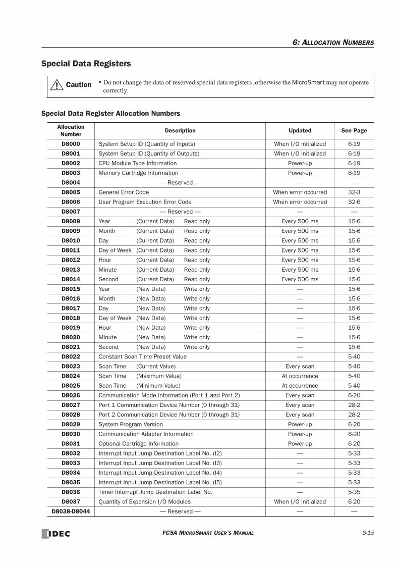
6: ALLOCATION NUMBERS
Special Data Registers
Special Data Register Allocation Numbers
• Do not change the data of reserved special data registers, otherwise the MicroSmart may not operate correctly.
Allocation Number
Description Updated See Page
D8000 System Setup ID (Quantity of Inputs) When I/O initialized 6-19
D8001 System Setup ID (Quantity of Outputs) When I/O initialized 6-19
D8002 CPU Module Type Information Power-up 6-19
D8003 Memory Cartridge Information Power-up 6-19
D8004 — Reserved — — —
D8005 General Error Code When error occurred 32-3
D8006 User Program Execution Error Code When error occurred 32-6
D8007 — Reserved — — —
D8008 Year (Current Data) Read only Every 500 ms 15-6
D8009 Month (Current Data) Read only Every 500 ms 15-6
D8010 Day (Current Data) Read only Every 500 ms 15-6
D8011 Day of Week (Current Data) Read only Every 500 ms 15-6
D8012 Hour (Current Data) Read only Every 500 ms 15-6
D8013 Minute (Current Data) Read only Every 500 ms 15-6
D8014 Second (Current Data) Read only Every 500 ms 15-6
D8015 Year (New Data) Write only — 15-6
D8016 Month (New Data) Write only — 15-6
D8017 Day (New Data) Write only — 15-6
D8018 Day of Week (New Data) Write only — 15-6
D8019 Hour (New Data) Write only — 15-6
D8020 Minute (New Data) Write only — 15-6
D8021 Second (New Data) Write only — 15-6
D8022 Constant Scan Time Preset Value — 5-40
D8023 Scan Time (Current Value) Every scan 5-40
D8024 Scan Time (Maximum Value) At occurrence 5-40
D8025 Scan Time (Minimum Value) At occurrence 5-40
D8026 Communication Mode Information (Port 1 and Port 2) Every scan 6-20
D8027 Port 1 Communication Device Number (0 through 31) Every scan 28-2
D8028 Port 2 Communication Device Number (0 through 31) Every scan 28-2
D8029 System Program Version Power-up 6-20
D8030 Communication Adapter Information Power-up 6-20
D8031 Optional Cartridge Information Power-up 6-20
D8032 Interrupt Input Jump Destination Label No. (I2) — 5-33
D8033 Interrupt Input Jump Destination Label No. (I3) — 5-33
D8034 Interrupt Input Jump Destination Label No. (I4) — 5-33
D8035 Interrupt Input Jump Destination Label No. (I5) — 5-33
D8036 Timer Interrupt Jump Destination Label No. — 5-35
D8037 Quantity of Expansion I/O Modules When I/O initialized 6-20
D8038-D8044 — Reserved — — —
Caution
FC5A MICROSMART USER’S MANUAL 6-15

6: ALLOCATION NUMBERS
Special Data Registers for High-speed Counters (All-in-one type CPU modules only)
Special Data Registers for Modbus Communication
Special Data Registers for Pulse Outputs
Special Data Registers for Analog Potentiometers
Special Data Registers for High-speed Counters
Special Data Register for HMI Module
Allocation Number
Description Updated See Page
D8045 High-speed Counter 1 (I0-I2) Current Value Every scan 5-7, 5-9
D8046 High-speed Counter 1 (I0-I2) Reset Value — 5-7, 5-9
D8047 High-speed Counter 2 (I3) Current Value Every scan 5-7
D8048 High-speed Counter 2 (I3) Preset Value — 5-7
D8049 High-speed Counter 3 (I4) Current Value Every scan 5-7
D8050 High-speed Counter 3 (I4) Preset Value — 5-7
D8051 High-speed Counter 4 (I5-I7) Current Value Every scan 5-7
D8052 High-speed Counter 4 (I5-I7) Reset Value — 5-7
D8053 Modbus communication error code Every scan 30-7, 30-7
D8054 Modbus communication transmission wait timeWhen communication
initialized30-7, 30-7
D8055 Current Pulse Frequency of PULS1 or RAMP1 (Q0) Every scan 20-4, 20-18
D8056 Current Pulse Frequency of PULS2 or RAMP1 (Q1) Every scan 20-4, 20-18
D8059 Current Pulse Frequency of PULS3 or RAMP2 (Q2) Every scan 20-4, 20-18
D8057 Analog Potentiometer 1 Value (All CPU modules) Every scan 5-48
D8058Analog Potentiometer 2 Value (All-in-one 24-I/O type CPU) Analog Voltage Input (Slim type CPU modules)
Every scan 5-48, 5-49
D8060Frequency Measurement Value I1 (All-in-one type CPU)Frequency Measurement Value I1 High Word (Slim type CPU)
Every scan 5-29
D8061— Reserved (All-in-one type CPU) —
Frequency Measurement Value I1 Low Word (Slim type CPU)Every scan 5-29
D8062Frequency Measurement Value I3 (All-in-one type CPU)Frequency Measurement Value I3 High Word (Slim type CPU)
Every scan 5-29
D8063— Reserved (All-in-one type CPU) —
Frequency Measurement Value I3 Low Word (Slim type CPU)Every scan 5-29
D8064Frequency Measurement Value I4 (All-in-one type CPU)Frequency Measurement Value I4 High Word (Slim type CPU)
Every scan 5-29
D8065— Reserved (All-in-one type CPU) —
Frequency Measurement Value I4 Low Word (Slim type CPU)Every scan 5-29
D8066Frequency Measurement Value I5 (All-in-one type CPU)Frequency Measurement Value I7 High Word (Slim type CPU)
Every scan 5-29
D8067— Reserved (All-in-one type CPU) —
Frequency Measurement Value I7 Low Word (Slim type CPU)Every scan 5-29
D8068 HMI Module Initial Screen Selection Power-up 5-52
6-16 FC5A MICROSMART USER’S MANUAL

6: ALLOCATION NUMBERS
Special Data Registers for Data Link Master/Slave Stations and Modbus Master Station
Allocation Number
Description Updated See Page
D8069Slave Station 1 Communication Error (at Master Station) Slave Station Communication Error (at Slave Station)Error station number and error code (at Modbus Master)
When error occurred 27-4, 30-7
D8070Slave Station 2 Communication Error (at Master Station)Error station number and error code (at Modbus Master)
When error occurred 27-4, 30-7
D8071Slave Station 3 Communication Error (at Master Station)Error station number and error code (at Modbus Master)
When error occurred 27-4, 30-7
D8072Slave Station 4 Communication Error (at Master Station)Error station number and error code (at Modbus Master)
When error occurred 27-4, 30-7
D8073Slave Station 5 Communication Error (at Master Station)Error station number and error code (at Modbus Master)
When error occurred 27-4, 30-7
D8074Slave Station 6 Communication Error (at Master Station)Error station number and error code (at Modbus Master)
When error occurred 27-4, 30-7
D8075Slave Station 7 Communication Error (at Master Station)Error station number and error code (at Modbus Master)
When error occurred 27-4, 30-7
D8076Slave Station 8 Communication Error (at Master Station)Error station number and error code (at Modbus Master)
When error occurred 27-4, 30-7
D8077Slave Station 9 Communication Error (at Master Station)Error station number and error code (at Modbus Master)
When error occurred 27-4, 30-7
D8078Slave Station 10 Communication Error (at Master Station)Error station number and error code (at Modbus Master)
When error occurred 27-4, 30-7
D8079Slave Station 11 Communication Error (at Master Station)Error station number and error code (at Modbus Master)
When error occurred 27-4, 30-7
D8080Slave Station 12 Communication Error (at Master Station)Error station number and error code (at Modbus Master)
When error occurred 27-4, 30-7
D8081Slave Station 13 Communication Error (at Master Station)Error station number and error code (at Modbus Master)
When error occurred 27-4, 30-7
D8082Slave Station 14 Communication Error (at Master Station)Error station number and error code (at Modbus Master)
When error occurred 27-4, 30-7
D8083Slave Station 15 Communication Error (at Master Station)Error station number and error code (at Modbus Master)
When error occurred 27-4, 30-7
D8084Slave Station 16 Communication Error (at Master Station)Error station number and error code (at Modbus Master)
When error occurred 27-4, 30-7
D8085Slave Station 17 Communication Error (at Master Station)Error station number and error code (at Modbus Master)
When error occurred 27-4, 30-7
D8086Slave Station 18 Communication Error (at Master Station)Error station number and error code (at Modbus Master)
When error occurred 27-4, 30-7
D8087Slave Station 19 Communication Error (at Master Station)Error station number and error code (at Modbus Master)
When error occurred 27-4, 30-7
D8088Slave Station 20 Communication Error (at Master Station)Error station number and error code (at Modbus Master)
When error occurred 27-4, 30-7
D8089Slave Station 21 Communication Error (at Master Station)Error station number and error code (at Modbus Master)
When error occurred 27-4, 30-7
D8090Slave Station 22 Communication Error (at Master Station)Error station number and error code (at Modbus Master)
When error occurred 27-4, 30-7
D8091Slave Station 23 Communication Error (at Master Station)Error station number and error code (at Modbus Master)
When error occurred 27-4, 30-7
D8092Slave Station 24 Communication Error (at Master Station)Error station number and error code (at Modbus Master)
When error occurred 27-4, 30-7
FC5A MICROSMART USER’S MANUAL 6-17

6: ALLOCATION NUMBERS
Special Data Registers for Communication Ports (D8200-D8209: Slim type CPU modules only)
Special Data Registers for High-speed Counters (Slim type CPU modules only)
D8093Slave Station 25 Communication Error (at Master Station)Error station number and error code (at Modbus Master)
When error occurred 27-4, 30-7
D8094Slave Station 26 Communication Error (at Master Station)Error station number and error code (at Modbus Master)
When error occurred 27-4, 30-7
D8095Slave Station 27 Communication Error (at Master Station)Error station number and error code (at Modbus Master)
When error occurred 27-4, 30-7
D8096Slave Station 28 Communication Error (at Master Station)Error station number and error code (at Modbus Master)
When error occurred 27-4, 30-7
D8097Slave Station 29 Communication Error (at Master Station)Error station number and error code (at Modbus Master)
When error occurred 27-4, 30-7
D8098Slave Station 30 Communication Error (at Master Station)Error station number and error code (at Modbus Master)
When error occurred 27-4, 30-7
D8099Slave Station 31 Communication Error (at Master Station)Error station number and error code (at Modbus Master)
When error occurred 27-4, 30-7
D8100 Data Link Slave Station Number Every scan 27-8
D8101 Data Link Transmit Wait Time (ms) Every scan 27-12
D8102 — Reserved — — —
D8103 Online Mode Protocol Selection When sending/receiving data 29-3
D8104 RS232C Control Signal Status (Port 2) Every scan 17-29
D8105 RS232C DSR Input Control Signal Option (Port 2) When sending/receiving data 17-30
D8106 RS232C DTR Output Control Signal Option (Port 2) When sending/receiving data 17-30
D8107-D8108 — Reserved — — —
D8109 Retry Cycles At retry 29-3
D8110 Retry Interval Every scan during retry 29-3
D8111 Modem Mode Status At status transition 29-3
D8112-D8114 — Reserved — — —
D8115-D8129 AT Command Result Code When returning result code 29-3
D8130-D8144 AT Command String When sending AT command 29-3
D8145-D8169 Initialization String When sending init. string 29-3
D8170-D8199 Telephone Number When dialing 29-3
D8200-D8209 — Reserved — — —
D8210 High-speed Counter 1 (I0-I2) Current Value (high word) Every scan 5-16, 5-19
D8211 High-speed Counter 1 (I0-I2) Current Value (low word) Every scan 5-16, 5-19
D8212 High-speed Counter 1 (I0-I2) Preset Value 1 (high word) Every scan 5-16, 5-19
D8213 High-speed Counter 1 (I0-I2) Preset Value 1 (low word) Every scan 5-16, 5-19
D8214 High-speed Counter 1 (I0-I2) Preset Value 2 (high word) Every scan 5-16, 5-19
D8215 High-speed Counter 1 (I0-I2) Preset Value 2 (low word) Every scan 5-16, 5-19
D8216 High-speed Counter 1 (I0-I2) Reset Value (high word) Every scan 5-16, 5-19
D8217 High-speed Counter 1 (I0-I2) Reset Value (low word) Every scan 5-16, 5-19
D8218 High-speed Counter 2 (I3) Current Value (high word) Every scan 5-16
D8219 High-speed Counter 2 (I3) Current Value (low word) Every scan 5-16
D8220 High-speed Counter 2 (I3) Preset Value (high word) Every scan 5-16
Allocation Number
Description Updated See Page
6-18 FC5A MICROSMART USER’S MANUAL

6: ALLOCATION NUMBERS
Special Data Register for Expansion Interface Module (Slim type CPU modules only)
D8000 System Setup ID (Quantity of Inputs)
The total of input points provided on the CPU module and connected expansion input modules is stored to D8000. When a mixed I/O module (4 inputs and 4 outputs) is connected, 8 input points are added to the total.
D8001 System Setup ID (Quantity of Outputs)
The total of output points provided on the CPU module and connected expansion output modules is stored to D8001. When a mixed I/O module (4 inputs and 4 outputs) is connected, 8 output points are added to the total.
D8002 CPU Module Type Information
Information about the CPU module type is stored to D8002.
0: FC5A-C10R2 or FC5A-C10R2C 1: FC5A-C16R2 or FC5A-C16R2C 3: FC5A-C24R2 or FC5A-C24R2C 4: FC5A-D32K3 or FC5A-D32S3 6: FC5A-D16RK1 or FC5A-D16RS1
D8003 Memory Cartridge Information
When an optional memory cartridge is installed on the CPU module cartridge connector, information about the user pro-gram stored on the memory cartridge is stored to D8003.
0: FC5A-C10R2 or FC5A-C10R2C 1: FC5A-C16R2 or FC5A-C16R2C 3: FC5A-C24R2 or FC5A-C24R2C 4: FC5A-D32K3 or FC5A-D32S3 6: FC5A-D16RK1 or FC5A-D16RS1 255: The memory cartridge does not store any user program.
Allocation Number
Description Updated See Page
D8221 High-speed Counter 2 (I3) Preset Value (low word) Every scan 5-16
D8222 High-speed Counter 3 (I4) Current Value (high word) Every scan 5-16
D8223 High-speed Counter 3 (I4) Current Value (low word) Every scan 5-16
D8224 High-speed Counter 3 (I4) Preset Value (high word) Every scan 5-16
D8225 High-speed Counter 3 (I4) Preset Value (low word) Every scan 5-16
D8226 High-speed Counter 4 (I5-I7) Current Value (high word) Every scan 5-16, 5-19
D8227 High-speed Counter 4 (I5-I7) Current Value (low word) Every scan 5-16, 5-19
D8228 High-speed Counter 4 (I5-I7) Preset Value 1 (high word) Every scan 5-16, 5-19
D8229 High-speed Counter 4 (I5-I7) Preset Value 1 (low word) Every scan 5-16, 5-19
D8230 High-speed Counter 4 (I5-I7) Preset Value 2 (high word) Every scan 5-16, 5-19
D8231 High-speed Counter 4 (I5-I7) Preset Value 2 (low word) Every scan 5-16, 5-19
D8232 High-speed Counter 4 (I5-I7) Reset Value (high word) Every scan 5-16, 5-19
D8233 High-speed Counter 4 (I5-I7) Reset Value (low word) Every scan 5-16, 5-19
D8234-D8251 — Reserved — — —
D8252 Expansion Interface Module I/O Refresh Time (×100 µs) Every scan 2-61
D8253-D8499 — Reserved — — —
FC5A MICROSMART USER’S MANUAL 6-19

6: ALLOCATION NUMBERS
D8026 Communication Mode Information (Port 1 and Port 2)
Communication mode information of port 1 and port 2 is stored to D8026.
D8029 System Program Version
The PLC system program version number is stored to D8029. This value is indicated in the PLC status dialog box called from the WindLDR menu bar. Select Online > Monitor, then select Online > PLC Status. See page 32-1.
D8030 Communication Adapter Information
Information about the communication adapter installed on the port 2 connector is stored to D8030.
0: RS232C communication adapter is installed 1: RS485 communication adapter is installed or no communication adapter is installed
D8031 Optional Cartridge Information
Information about the optional cartridge installed on the CPU module is stored to D8031.
0: No optional cartridge is installed 1: Clock cartridge is installed 2: Memory cartridge is installed 3: Clock cartridge and memory cartridge are installed
D8037 Quantity of Expansion I/O Modules
The quantity of expansion I/O modules connected to the all-in-one 24-I/O type CPU module or any slim type CPU module is stored to D8037.
D8104 RS232C Control Signal Status (Port 2)
RS232C control signal status of port 2 is stored to D8104.
Bit 15
02
01
00
Port 2 000: Maintenance Protocol 001: User Protocol 010: Data Link 011: Modem Protocol 100: Modbus Slave RTU Communication 101: Modbus Slave ASCII Communication 110: Modbus Master RTU Communication 111: Modbus Master ASCII Communication
Port 1 0: Maintenance Protocol 1: User Protocol
D8026 03
Bit 15
01
00
00: Both DSR and DTR are off01: DTR is on 10: DSR is on 11: Both DSR and DTR are on
D8104
Port 2
6-20 FC5A MICROSMART USER’S MANUAL

6: ALLOCATION NUMBERS
D8105 RS232C DSR Input Control Signal Option (Port 2)
Special data register D8105 is used to control data flow between the MicroSmart RS232C port 2 and the remote terminal depending on the DSR (data set ready) signal sent from the remote terminal.
D8106 RS232C DTR Output Control Signal Option (Port 2)
Special data register D8106 is used to control the DTR (data terminal ready) signal to indicate the MicroSmart operating status or transmitting/receiving status.
Bit 15
02
01
00
000: DSR is not used for data flow control 001: When DSR is on, MicroSmart can transmit and receive data010: When DSR is off, MicroSmart can transmit and receive data011: When DSR is on, MicroSmart can transmit data (busy control)010: When DSR is off, MicroSmart can transmit data Others: Same as 000
D8105
Port 2
Bit 15
01
00
00: DTR is on (off while MicroSmart is stopped) 01: DTR is off 10: DSR is on while MicroSmart can receive data (auto switching)11: Same as 00
D8106
Port 2
FC5A MICROSMART USER’S MANUAL 6-21

6: ALLOCATION NUMBERS
Expansion Data RegistersSlim type CPU modules FC5A-D16RK1, FC5A-D16RS1, FC5A-D32K3, and FC5A-D32S3 have expansion data registers D2000 through D7999. These expansion data registers are normally used as ordinary data registers to store numerical data while the CPU module is executing a user program. In addition, numerical data can be set to designated ranges of expan-sion data registers using the expansion data register editor on WindLDR. When the user program is downloaded from WindLDR to the CPU module, the preset values of the expansion data registers are also downloaded to the EEPROM in the CPU module. Each time the CPU is powered up, the preset values of the expansion data registers stored in the EEPROM are loaded to the RAM and the user program in the RAM is executed.
Since the data in the EEPROM is non-volatile, the preset values of the expansion data registers are maintained semi-per-manently and restored in the RAM each time the CPU is powered up. This feature is useful when particular numerical data must not be lost. Furthermore, data register values can be easily entered in the form of either numbers or character strings using the expansion data register editor on WindLDR.
Programming WindLDR
1. From the WindLDR menu bar, select Configure > Expansion Data Register Settings.
The Expansion Data Register Settings dialog box appears.
2. Click the check box to use the preset range 1 or 2.
Among expansion data registers D2000 through D7999, two ranges can be specified for preset data registers.
Use Preset Range 1 or 2: Click the check box, and type the first data register number in the DR No. box and the quan-tity of data registers to store preset values in the Quantity box.
Use Initializing Relay: Click the check box and specify an internal relay number to use as an initializing relay. When the initializing relay is turned on while the CPU is powered up, the preset values of the expansion data registers in the EEPROM are loaded to the RAM.
Use Backup Relay: Click the check box and specify an internal relay number to use as a backup relay. When the backup relay is turned on while the CPU is powered up, the values of the preset expansion data registers in the RAM overwrite the preset values in the EEPROM.
First Data Register No.
Edit ButtonGo to the expansion data
register editor screen.
Quantity of Data Registers
Copy RangeCopy the data between User Pre-set Ranges 1 and 2.
6-22 FC5A MICROSMART USER’S MANUAL

6: ALLOCATION NUMBERS
3. Click the Edit button. The Edit Expansion Data Registers screen appears.
The specified quantity of data registers are reserved to store preset values in the Edit Expansion Data Registers screen. You can enter numerical values to these data registers individually, in the form of character strings, or fill the same value to consecutive data registers.
Enter Individual ValuesClick the data register number in the Edit Expansion Data Registers screen where you want to enter a numerical value, and type a value 0 through 65535. When finished, click OK to return to the Expansion Data Register Settings dialog box.
Enter Character StringClick the right mouse button at the data register number in the Edit Expansion Data Registers screen where you want to enter a character string. A pop-up menu appears. Select String in the pop-up menu, then the String dialog box appears. Type required characters, and click OK. The entered characters are converted in pairs into ASCII decimal values and stored to data registers, starting with the selected data register number.
Fill Same ValueClick the right mouse button at the data register number in the Edit Expansion Data Registers screen where you want to enter numerical values. A pop-up menu appears. Select Fill in the pop-up menu, then the Fill dialog box appears. Type the first data register number, the quantity of data registers, and the value. When fin-ished, click OK. The value is entered to consecutive data registers.
4. After editing the preset values of expansion data registers, download the user program to the CPU module since these settings relate to the user program.
First Data Register No.
Select a notation to show the data in decimal, hexadecimal, or ASCII characters on the Edit Expansion Data Register screen.
FC5A MICROSMART USER’S MANUAL 6-23
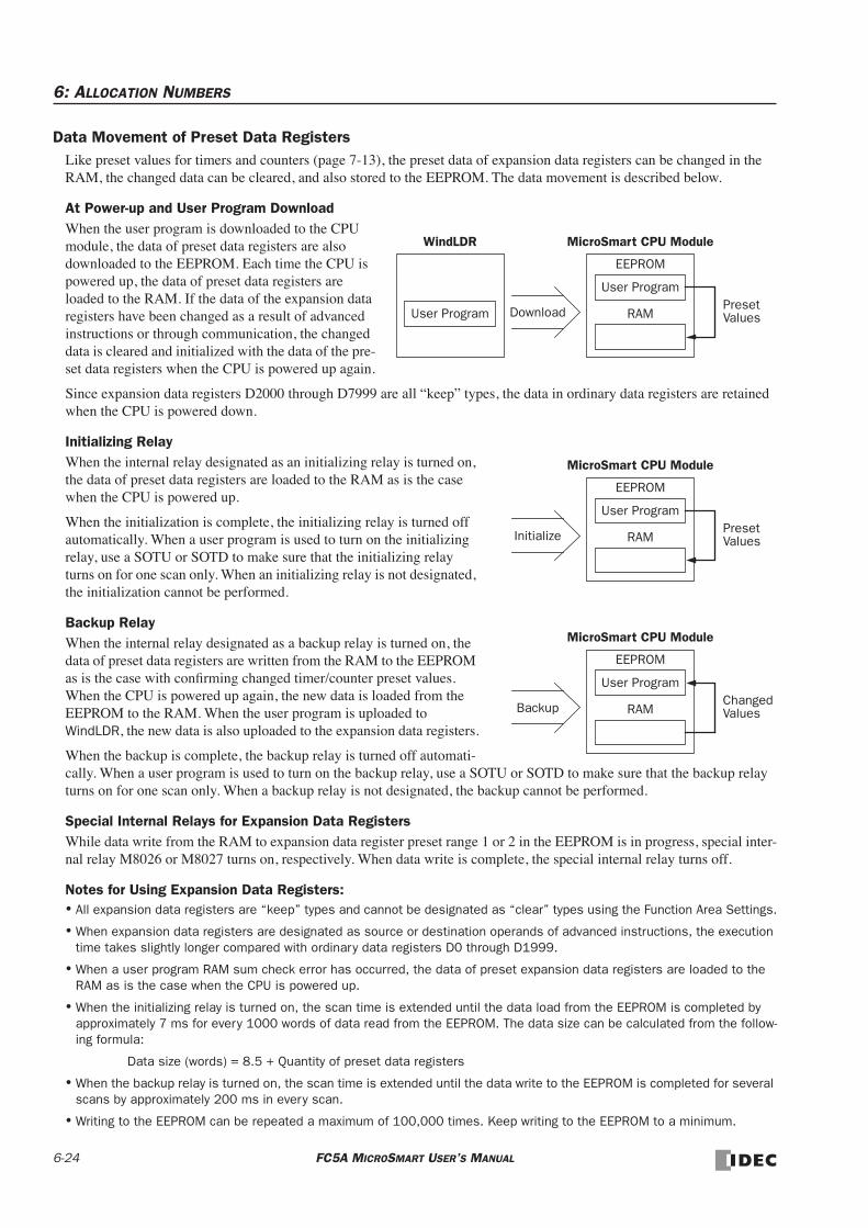
6: ALLOCATION NUMBERS
Data Movement of Preset Data RegistersLike preset values for timers and counters (page 7-13), the preset data of expansion data registers can be changed in the RAM, the changed data can be cleared, and also stored to the EEPROM. The data movement is described below.
At Power-up and User Program DownloadWhen the user program is downloaded to the CPU module, the data of preset data registers are also downloaded to the EEPROM. Each time the CPU is powered up, the data of preset data registers are loaded to the RAM. If the data of the expansion data registers have been changed as a result of advanced instructions or through communication, the changed data is cleared and initialized with the data of the pre-set data registers when the CPU is powered up again.
Since expansion data registers D2000 through D7999 are all “keep” types, the data in ordinary data registers are retained when the CPU is powered down.
Initializing RelayWhen the internal relay designated as an initializing relay is turned on, the data of preset data registers are loaded to the RAM as is the case when the CPU is powered up.
When the initialization is complete, the initializing relay is turned off automatically. When a user program is used to turn on the initializing relay, use a SOTU or SOTD to make sure that the initializing relay turns on for one scan only. When an initializing relay is not designated, the initialization cannot be performed.
Backup RelayWhen the internal relay designated as a backup relay is turned on, the data of preset data registers are written from the RAM to the EEPROM as is the case with confirming changed timer/counter preset values. When the CPU is powered up again, the new data is loaded from the EEPROM to the RAM. When the user program is uploaded to WindLDR, the new data is also uploaded to the expansion data registers.
When the backup is complete, the backup relay is turned off automati-cally. When a user program is used to turn on the backup relay, use a SOTU or SOTD to make sure that the backup relay turns on for one scan only. When a backup relay is not designated, the backup cannot be performed.
Special Internal Relays for Expansion Data RegistersWhile data write from the RAM to expansion data register preset range 1 or 2 in the EEPROM is in progress, special inter-nal relay M8026 or M8027 turns on, respectively. When data write is complete, the special internal relay turns off.
Notes for Using Expansion Data Registers:• All expansion data registers are “keep” types and cannot be designated as “clear” types using the Function Area Settings.
• When expansion data registers are designated as source or destination operands of advanced instructions, the execution time takes slightly longer compared with ordinary data registers D0 through D1999.
• When a user program RAM sum check error has occurred, the data of preset expansion data registers are loaded to the RAM as is the case when the CPU is powered up.
• When the initializing relay is turned on, the scan time is extended until the data load from the EEPROM is completed by approximately 7 ms for every 1000 words of data read from the EEPROM. The data size can be calculated from the follow-ing formula:
Data size (words) = 8.5 + Quantity of preset data registers
• When the backup relay is turned on, the scan time is extended until the data write to the EEPROM is completed for several scans by approximately 200 ms in every scan.
• Writing to the EEPROM can be repeated a maximum of 100,000 times. Keep writing to the EEPROM to a minimum.
WindLDR MicroSmart CPU Module
Download
User Program
EEPROM
RAMUser ProgramPresetValues
MicroSmart CPU Module
Initialize
User Program
EEPROM
RAMPresetValues
MicroSmart CPU Module
Backup
User Program
EEPROM
RAMChangedValues
6-24 FC5A MICROSMART USER’S MANUAL

6: ALLOCATION NUMBERS
Expansion I/O Module OperandsExpansion I/O modules are available in digital I/O modules and analog I/O modules.
Among the all-in-one type CPU modules, only the 24-I/O type CPU modules (FC5A-C24R2 and FC5A-C24R2C) can connect a maximum of four expansion I/O modules including analog I/O modules.
All slim type CPU modules can connect a maximum of seven expansion I/O modules including analog I/O modules. When using the expansion interface module, another eight expansion I/O modules can be added.
I/O Expansion for All-in-One Type CPU ModulesA maximum of four input, output, mixed I/O, or analog I/O modules can be mounted with the 24-I/O type CPU module, so that the I/O points can be expanded to a maximum of 78 inputs or 74 outputs. The total of inputs and outputs can be a max-imum of 88 points. Input and output numbers are automatically allocated to each digital I/O module, starting with I30 and Q30, in the order of increasing distance from the CPU module. Expansion I/O modules cannot be mounted with the 10- and 16-I/O type CPU modules (FC5A-C10R2, FC5A-C10R2C, FC5A-C16R2, and FC5A-C16R2C).
I/O Allocation Numbers (All-in-One Type CPU Modules)
Example:
The system setup shown above will have I/O operand numbers allocated for each module as follows:
The I/O numbers of the CPU module start with I0 and Q0. The I/O numbers of the expansion I/O modules start with I30 and Q30. The mixed I/O module has 4 inputs and 4 outputs. When an I/O module is mounted next to a mixed I/O module, note that the allocation numbers skip four points as shown above.
Input and output modules may be grouped together for easy identification of I/O numbers. When the I/O modules are relo-cated, the I/O numbers are renumbered automatically.
OperandFC5A-C10R2FC5A-C10R2C
FC5A-C16R2FC5A-C16R2C
FC5A-C24R2FC5A-C24R2C
Allocation No. Points Allocation No. Points Allocation No. Points
Input (I) I0 - I5 6I0 - I7I10
9I0 - I7I10 - I15
1478 total
Expansion Input (I) — — — — I30 - I107 64
Output (Q) Q0 - Q3 4 Q0 - Q6 7Q0 - Q7Q10 - Q11
1074 total
Expansion Output (Q) — — — — Q30 - Q107 64
Slot No. Module I/O Operand Numbers
24-I/O Type CPU Module I0 to I7, I10 to I15, Q0 to Q7, Q10 and Q11
1 16-pt Input Module I30 to I37, I40 to I47
2 Analog I/O Module See page 26-8.
3 4/4-pt Mixed I/O Module I50 to I53, Q30 to Q33
4 8-pt Input Module I60 to I67
24-I/O Type Input
16-ptInput
Analog Mixed
4-ptInput
Input
8-ptInput
Slot No.: 1 2 3 4
Module I/O I/O Module
4-ptOutput
14-pt Input10-pt Output
CPU Module
Expansion I/O Modules (4 maximum)
ModuleModule
FC5A MICROSMART USER’S MANUAL 6-25
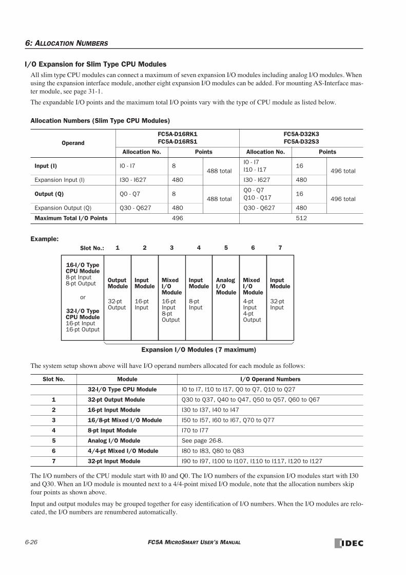
6: ALLOCATION NUMBERS
I/O Expansion for Slim Type CPU ModulesAll slim type CPU modules can connect a maximum of seven expansion I/O modules including analog I/O modules. When using the expansion interface module, another eight expansion I/O modules can be added. For mounting AS-Interface mas-ter module, see page 31-1.
The expandable I/O points and the maximum total I/O points vary with the type of CPU module as listed below.
Allocation Numbers (Slim Type CPU Modules)
Example:
The system setup shown above will have I/O operand numbers allocated for each module as follows:
The I/O numbers of the CPU module start with I0 and Q0. The I/O numbers of the expansion I/O modules start with I30 and Q30. When an I/O module is mounted next to a 4/4-point mixed I/O module, note that the allocation numbers skip four points as shown above.
Input and output modules may be grouped together for easy identification of I/O numbers. When the I/O modules are relo-cated, the I/O numbers are renumbered automatically.
OperandFC5A-D16RK1FC5A-D16RS1
FC5A-D32K3FC5A-D32S3
Allocation No. Points Allocation No. Points
Input (I) I0 - I7 8488 total
I0 - I7I10 - I17
16496 total
Expansion Input (I) I30 - I627 480 I30 - I627 480
Output (Q) Q0 - Q7 8488 total
Q0 - Q7Q10 - Q17
16496 total
Expansion Output (Q) Q30 - Q627 480 Q30 - Q627 480
Maximum Total I/O Points 496 512
Slot No. Module I/O Operand Numbers
32-I/O Type CPU Module I0 to I7, I10 to I17, Q0 to Q7, Q10 to Q27
1 32-pt Output Module Q30 to Q37, Q40 to Q47, Q50 to Q57, Q60 to Q67
2 16-pt Input Module I30 to I37, I40 to I47
3 16/8-pt Mixed I/O Module I50 to I57, I60 to I67, Q70 to Q77
4 8-pt Input Module I70 to I77
5 Analog I/O Module See page 26-8.
6 4/4-pt Mixed I/O Module I80 to I83, Q80 to Q83
7 32-pt Input Module I90 to I97, I100 to I107, I110 to I117, I120 to I127
Output
32-ptOutput
AnalogMixed
16-ptInput
Input
8-ptInput
Slot No.: 1 2 3 4
Module I/OI/O Module
8-ptOutput
Expansion I/O Modules (7 maximum)
Module Moduleor
5 6
Input
32-ptInput
7
ModuleInput
16-ptInput
ModuleMixed
4-ptInput
I/O
4-ptOutput
Module
16-I/O Type
8-pt Input8-pt Output
CPU Module
32-I/O Type
16-pt Input16-pt Output
CPU Module
6-26 FC5A MICROSMART USER’S MANUAL

7: BASIC INSTRUCTIONS
IntroductionThis chapter describes programming of the basic instructions, available operands, and sample programs.
All basic instructions are available on all MicroSmart CPU modules.
Basic Instruction List
Symbol Name FunctionSee Page
AND And Series connection of NO contact 7-4
AND LOD And Load Series connection of circuit blocks 7-5
ANDN And Not Series connection of NC contact 7-4
BPP Bit PopRestores the result of bit logical operation which was saved tem-porarily
7-6
BPS Bit Push Saves the result of bit logical operation temporarily 7-6
BRD Bit ReadReads the result of bit logical operation which was saved tempo-rarily
7-6
CC= Counter Comparison (=) Equal to comparison of counter current value 7-14
CC≥ Counter Comparison (≥) Greater than or equal to comparison of counter current value 7-14
CDP Dual Pulse Reversible Counter Dual pulse reversible counter (0 to 65535) 7-10
CNT Adding Counter Adding counter (0 to 65535) 7-10
CUDUp/Down Selection Reversible Counter
Up/down selection reversible counter (0 to 65535) 7-10
DC= Data Register Comparison (=) Equal to comparison of data register value 7-16
DC≥ Data Register Comparison (≥) Greater than or equal to comparison of data register value 7-16
END End Ends a program 7-26
JEND Jump End Ends a jump instruction 7-25
JMP Jump Jumps a designated program area 7-25
LOD Load Stores intermediate results and reads contact status 7-2
LODN Load Not Stores intermediate results and reads inverted contact status 7-2
MCR Master Control Reset Ends a master control 7-23
MCS Master Control Set Starts a master control 7-23
OR Or Parallel connection of NO contact 7-4
OR LOD Or Load Parallel connection of circuit blocks 7-5
ORN Or Not Parallel connection of NC contact 7-4
OUT Output Outputs the result of bit logical operation 7-2
OUTN Output Not Outputs the inverted result of bit logical operation 7-2
RST Reset Resets output, internal relay, or shift register bit 7-3
SET Set Sets output, internal relay, or shift register bit 7-3
SFR Shift Register Forward shift register 7-18
SFRN Shift Register Not Reverse shift register 7-18
SOTD Single Output Down Falling-edge differentiation output 7-22
SOTU Single Output Up Rising-edge differentiation output 7-22
TIM 100-ms Timer Subtracting 100-ms timer (0 to 6553.5 sec) 7-7
TMH 10-ms Timer Subtracting 10-ms timer (0 to 655.35 sec) 7-7
TML 1-sec Timer Subtracting 1-sec timer (0 to 65535 sec) 7-7
TMS 1-ms Timer Subtracting 1-ms timer (0 to 65.535 sec) 7-7
FC5A MICROSMART USER’S MANUAL 7-1

7: BASIC INSTRUCTIONS
LOD (Load) and LODN (Load Not)The LOD instruction starts the logical operation with a NO (normally open) contact. The LODN instruction starts the log-ical operation with a NC (normally closed) contact.
A total of eight LOD and/or LODN instructions can be programmed consecutively.
OUT (Output) and OUTN (Output Not)The OUT instruction outputs the result of bit logical operation to the specified operand. The OUTN instruction outputs the inverted result of bit logical operation to the specified operand.
Multiple OUT and OUTNThere is no limit to the number of OUT and OUTN instructions that can be programmed into one rung.
Programming multiple outputs of the same output number is not recommended. How-ever, when doing so, it is good practice to separate the outputs with the JMP/JEND set of instructions, or the MCS/MCR set of instructions. These instructions are detailed later in this chapter.
When the same output number is programmed more than once within one scan, the out-put nearest to the END instruction is given priority for outputting. In the example on the right, output Q0 is off.
Ladder Diagram Valid Operands
The valid operand range depends on the CPU module type. For details, see pages 6-1 and 6-2.Data registers can be used as bit operands with the data register number and the bit position separated by a period.
Instruction I Q M T C R DLODLODN
0-627 0-627 0-2557
8000-83170-255 0-255 0-255 0.0-49999.15
Ladder Diagram Valid Operands
The valid operand range depends on the CPU module type. For details, see pages 6-1 and 6-2.Data registers can be used as bit operands with the data register number and the bit position separated by a period.
Instruction I Q M T C R DOUTOUTN
— 0-627 0-2557
8000-8317— — — 0.0-49999.15
Caution • For restrictions on ladder programming of OUT and OUTN instructions, see page 7-27.
Ladder Diagram
I1 I2 Q0
Q1
Q2
Ladder Diagram
I1
I2
I3
END
ON
OFF
OFF
Q0
Q0
OFF
7-2 FC5A MICROSMART USER’S MANUAL

7: BASIC INSTRUCTIONS
Examples: LOD (Load), OUT (Output), and NOT
SET and RST (Reset)The SET and RST (reset) instructions are used to set (on) or reset (off) outputs, internal relays, and shift register bits. The same output can be set and reset many times within a program. SET and RST instructions operate in every scan while the input is on.
Ladder Diagram
I0
Instruction DataLODOUTLODOUTN
I0Q0I1Q1
Program List
I0ON
OFF
I1ON
OFF
Q0ON
OFF
Q1ON
OFF
Timing Chart
Q0
Q1I1
Ladder Diagram
M2
Instruction DataLODOUT
M2Q0
Program List
Ladder Diagram
Q0
Instruction DataLODNOUT
Q0Q1
Program List
Ladder Diagram
T0
Instruction DataLODOUTN
T0Q2
Program List
Ladder Diagram
Instruction DataLODNOUT
C1Q10
Program List
C1
Q0
Q10
Q1
Q2
Caution
Ladder Diagram
I0
I1
I0ON
OFF
I1ON
OFF
Q0ON
OFF
Timing Chart
Instruction DataLODSETLODRST
I0Q0I1Q0
Program List
Valid Operands
The valid operand range depends on the CPU module type. For details, see pages 6-1 and 6-2.
Instruction I Q M T C R DSETRST
— 0-627 0-2557
8000-8317— — 0-255 0.0-49999.15
Q0S
Q0R
• For restrictions on ladder programming of SET and RST instructions, see page 7-27.
FC5A MICROSMART USER’S MANUAL 7-3

7: BASIC INSTRUCTIONS
AND and ANDN (And Not)The AND instruction is used for programming a NO contact in series. The ANDN instruction is used for programming a NC contact in series. The AND or ANDN instruction is entered after the first set of contacts.
OR and ORN (Or Not)The OR instruction is used for programming a NO contact in parallel. The ORN instruction is used for programming a NC contact in parallel. The OR or ORN instruction is entered after the first set of contacts.
Ladder Diagram
I0
Instruction DataLODANDOUTLODANDNOUT
I0I1Q0I0I1Q1
Program List
I1
I1I0
I0ON
OFF
I1ON
OFF
Q0ON
OFF
Q1ON
OFF
Timing Chart
When both inputs I0 and I1 are on, output Q0 is on. When either input I0 or I1 is off, output Q0 is off.
When input I0 is on and input I1 is off, output Q1 is on. When either input I0 is off or input I1 is on, output Q1 is off.
Valid Operands
The valid operand range depends on the CPU module type. For details, see pages 6-1 and 6-2.Data registers can be used as bit operands with the data register number and the bit position separated by a period.
Instruction I Q M T C R DANDANDN
0-627 0-627 0-2557
8000-83170-255 0-255 0-255 0.0-49999.15
Q0
Q1
Ladder Diagram
I0
I0
I0ON
OFF
I1ON
OFF
Q0ON
OFF
Q1ON
OFF
Timing Chart
When either input I0 or I1 is on, output Q0 is on. When both inputs I0 and I1 are off, output Q0 is off.
When either input I0 is on or input I1 is off, output Q1 is on. When input I0 is off and input I1 is on, output Q1 is off.
I1
I1
Instruction DataLODOROUTLODORNOUT
I0I1Q0I0I1Q1
Program List
Valid Operands
The valid operand range depends on the CPU module type. For details, see pages 6-1 and 6-2.Data registers can be used as bit operands with the data register number and the bit position separated by a period.
Instruction I Q M T C R DORORN
0-627 0-627 0-2557
8000-83170-255 0-255 0-255 0.0-49999.15
Q0
Q1
7-4 FC5A MICROSMART USER’S MANUAL

7: BASIC INSTRUCTIONS
AND LOD (Load)The AND LOD instruction is used to connect, in series, two or more circuits starting with the LOD instruction. The AND LOD instruction is the equivalent of a “node” on a ladder diagram.
When using WindLDR, the user need not program the AND LOD instruction. The circuit in the ladder diagram shown below is converted into AND LOD when the ladder diagram is compiled.
OR LOD (Load)The OR LOD instruction is used to connect, in parallel, two or more circuits starting with the LOD instruction. The OR LOD instruction is the equivalent of a “node” on a ladder diagram.
When using WindLDR, the user need not program the OR LOD instruction. The circuit in the ladder diagram shown below is converted into OR LOD when the ladder diagram is compiled.
Ladder Diagram
I0 I2
I0ONOFF
I2ONOFF
I3ONOFF
Q0ONOFF
Timing Chart
When input I0 is on and either input I2 or I3 is on, output Q0 is on.
When input I0 is off or both inputs I2 and I3 are off, output Q0 is off.
I3
Instruction DataLODLODORANDLODOUT
I0I2I3
Q0
Program List
Q0
I2
I0 I1
I3
Ladder Diagram
I0ONOFF
I1ONOFF
I2ONOFF
I3ONOFF
Timing Chart
When both inputs I0 and I1 are on or both inputs I2 and I3 are on, output Q0 is on.
When either input I0 or I1 is off and either input I2 or I3 is off, output Q0 is off.
Q0ONOFF
Instruction DataLODANDLODANDORLODOUT
I0I1I2I3
Q0
Program List
Q0
FC5A MICROSMART USER’S MANUAL 7-5

7: BASIC INSTRUCTIONS
BPS (Bit Push), BRD (Bit Read), and BPP (Bit Pop)The BPS (bit push) instruction is used to save the result of bit logical operation temporarily. The BRD (bit read) instruction is used to read the result of bit logical operation which was saved temporarily. The BPP (bit pop) instruction is used to restore the result of bit logical operation which was saved temporarily.
When using WindLDR, the user need not program the BPS, BRD, and BPP instructions. The circuit in the ladder diagram shown below is converted into BPS, BRD, and BPP when the ladder diagram is compiled.
I0 I1
I2
Ladder Diagram
I0ONOFF
I1ONOFF
I2ONOFF
I3ONOFF
Timing Chart
Q1ONOFF
I3
Q2ONOFF
Q3ONOFF
When both inputs I0 and I1 are on, output Q1 is turned on.
When both inputs I0 and I2 are on, output Q2 is turned on.
When both inputs I0 and I3 are on, output Q3 is turned on.
BPS
BPP
BRD
Instruction DataLODBPSANDOUTBRDANDOUTBPPANDOUT
I0
I1Q1
I2Q2
I3Q3
Program List
Q1
Q2
Q3
7-6 FC5A MICROSMART USER’S MANUAL

7: BASIC INSTRUCTIONS
TML, TIM, TMH, and TMS (Timer)Four types of timedown timers are available; 1-sec timer TML, 100-ms timer TIM, 10-ms timer TMH, and 1-ms timer TMS. A total of 256 timers can be programmed in a user program for any type of CPU module. Each timer must be allo-cated to a unique number T0 through T255.
The valid operand range depends on the CPU module type. For details, see pages 6-1 and 6-2.The preset value can be 0 through 65535 and designated using a decimal constant or data register.
TML (1-sec Timer)
TIM (100-ms Timer)
TMH (10-ms Timer)
TMS (1-ms Timer)
Timer Allocation Number Range Increments Preset Value
TML (1-sec timer) T0 to T255 0 to 65535 sec 1 secConstant: 0 to 65535Data registers: D0 to D1999
D2000 to D7999 D10000 to D49999
TIM (100-ms timer) T0 to T255 0 to 6553.5 sec 100 ms
TMH (10-ms timer) T0 to T255 0 to 655.35 sec 10 ms
TMS (1-ms timer) T0 to T255 0 to 65.535 sec 1 ms
I1
I0
T0
Ladder Diagram (TML)
TML4
T0 I0ON
OFF
T0ON
OFF
I1ON
OFF
Q0ON
OFF
Timing Chart
4 sec
Instruction DataLODTML
LODANDOUT
I0T04I1T0Q0
Program List
Q0
I1
I0
T1
Ladder Diagram (TIM)
TIM20
T1 I0ON
OFF
T1ON
OFF
I1ON
OFF
Q1ON
OFF
Timing Chart
Instruction DataLODTIM
LODANDOUT
I0T120I1T1Q1
Program List
2 sec
Q1
I1
I0
T2
Ladder Diagram (TMH)
TMH100
T2 I0ON
OFF
T2ON
OFF
I1ON
OFF
Q2ON
OFF
Timing Chart
Instruction DataLODTMH
LODANDOUT
I0T2100I1T2Q2
Program List
1 sec
Q2
I1
I0
T3
Ladder Diagram (TMS)
TMS500
T3 I0ON
OFF
T3ON
OFF
I1ON
OFF
Q3ON
OFF
Timing Chart
Instruction DataLODTMS
LODANDOUT
I0T3500I1T3Q3
Program List
0.5 sec
Q3
FC5A MICROSMART USER’S MANUAL 7-7

7: BASIC INSTRUCTIONS
Timer CircuitThe preset value 0 through 65535 can be designated using a data register D0 through D1999 or D2000 through D7999; then the data of the data register becomes the preset value. Directly after the TML, TIM, TMH, or TMS instruction, the OUT, OUTN, SET, RST, TML, TIM, TMH, or TMS instruction can be programmed.
• Timedown from the preset value is initiated when the operation result directly before the timer input is on.
• The timer output turns on when the current value (timed value) reaches 0.
• The current value returns to the preset value when the timer input is off.
• Timer preset and current values can be changed using WindLDR without downloading the entire program to the CPU again. From the WindLDR menu bar, select Online > Monitor, then select Online > Point Write. To change a timer preset value, specify the timer number with a capital T and a new preset value. If the timer preset value is changed during timedown, the timer remains unchanged for that cycle. The change will be reflected in the next time cycle. To change a timer current value, specify the timer number with a small t and a new current value while the timer is in operation. The change takes effect immediately.
• If the timer preset value is changed to 0, then the timer stops operation, and the timer output is turned on immediately.
• If the current value is changed during timedown, the change becomes effective immediately.
• For the data movement when changing, confirming, and clearing preset values, see page 7-13. Preset values can also be changed and changed preset values can be confirmed using the HMI module. See pages 5-53 and 5-54.
Timer AccuracyTimer accuracy due to software configuration depends on three factors: timer input error, timer counting error, and timeout output error. These errors are not constant but vary with the user program and other causes.
Timer Input Error
The input status is read at the END processing and stored to the input RAM. So, an error occurs depending on the timing when the timer input turns on in a scan cycle. The same error occurs on the normal input and the catch input. The timer input error shown below does not include input delay caused by the hardware.
CautionI1
Ladder Diagram
TIMD10
T5 Instruction DataLODTIM
OUT
I1T5D10Q0
Program List
Q0• For restrictions on ladder programming
of timer instructions, see page 7-27.
Program Processing
Actual InputON
OFF
Input RAMON
OFF
Timer Start
Minimum Error
Tie
END
1 scan time
TIM END
Tet
Program Processing
Actual InputON
OFF
Input RAMON
OFF
Timer Start
Maximum Error
END
1 scan time
TIM END
Tet
TIM
Tie
When the input turns on immediately before the END processing, Tie is almost 0. Then the timer input error is only Tet (behind error) and is at its minimum.
When the input turns on immediately after the END pro-cessing, Tie is almost equal to one scan time. Then the timer input error is Tie + Tet = one scan time + Tet (behind error) and is at its maximum.
Tie: Time from input turning on to the END processing Tet: Time from the END processing to the timer instruction execution
7-8 FC5A MICROSMART USER’S MANUAL

7: BASIC INSTRUCTIONS
Timer Accuracy, continued
Timer Counting Error
Every timer instruction operation is individually based on asynchronous 16-bit reference timers. Therefore, an error occurs depending on the status of the asynchronous 16-bit timer when the timer instruction is executed.
Timeout Output Error
The output RAM status is set to the actual output when the END instruction is processed. So, an error occurs depending on the timing when the timeout output turns on in a scan cycle. The timeout output error shown below does not include output delay caused by the hardware.
Maximum and Minimum of Errors
Notes: Advance error does not occur at the timer input and timeout output. Tet + Tte = 1 scan time Increment is 1 sec (TML), 100 ms (TIM), 10 ms (TMH), or 1 ms (TMS). The maximum advance error is: Increment – 1 scan time The maximum behind error is: 3 scan times
The timer input error and timeout output error shown above do not include the input response time (behind error) and output response time (behind error) caused by hardware.
Power Failure Memory ProtectionTimers TML, TIM, TMH, and TMS do not have power failure protection. A timer with this protection can be devised using a counter instruction and special internal relay M8121 (1-sec clock), M8122 (100-ms clock), or M8123 (10-ms clock).
ErrorTML
(1-sec timer)TIM
(100-ms timer)TMH
(10-ms timer)TMS
(1-ms timer)
MaximumAdvance error 1000 ms 100 ms 10 ms 1 ms
Behind error 1 scan time 1 scan time 1 scan time 1 scan time
Error Timer Input ErrorTimer Counting
ErrorTimeout Output
ErrorTotal Error
MinimumAdvance error 0 (Note) 0 0 (Note) 0
Behind error Tet 0 Tte 0
MaximumAdvance error 0 (Note) Increment 0 (Note) Increment – (Tet + Tte)
Behind error 1 scan time + Tet 1 scan time Tte 2 scan times + (Tet + Tte)
Program Processing
Timeout Output RAMON
OFF
Actual OutputON
OFF
END
1 scan time
TIM END
Tte
Timeout output error is equal to Tte (behind error) and can be between 0 and one scan time.
0 < Tte < 1 scan time
Tte: Time from the timer instruction execution to the END processing
Ladder Diagram
I1
I1ON
OFF
C2ON
OFF
Timing Chart
10 sec
(10-sec Timer)
CNT C21000
M8123
Reset
Pulse
Instruction DataLODNLODCNT
I1M8123C21000
Program List
Note: Designate counter C2 used in this program as a keep type counter. See page 5-4.
FC5A MICROSMART USER’S MANUAL 7-9

7: BASIC INSTRUCTIONS
CNT, CDP, and CUD (Counter)Three types of counters are available; adding (up) counter CNT, dual-pulse reversible counter CDP, and up/down selection reversible counter CUD. A total of 256 counters can be programmed in a user program for any type of CPU module. Each counter must be allocated to a unique number C0 through C255.
The valid operand range depends on the CPU module type. For details, see pages 6-1 and 6-2.The preset value can be 0 through 65535 and designated using a decimal constant or data register.
CNT (Adding Counter)When counter instructions are programmed, two addresses are required. The circuit for an adding (UP) counter must be programmed in the following order: reset input, pulse input, the CNT instruction, and a counter number C0 through C255, followed by a counter preset value from 0 to 65535.
The preset value can be designated using a decimal constant or a data register. When a data register is used, the data of the data register becomes the preset value.
Counter Allocation Number Preset Value
CNT (adding counter) C0 to C255 Constant: 0 to 65535Data registers: D0 to D1999
D2000 to D7999 D10000 to D49999
CDP (dual-pulse reversible counter) C0 to C255
CUD (up/down selection reversible counter) C0 to C255
Ladder Diagram
I2
Reset Input I0ONOFF
Pulse Input I1ONOFF
Counter C0ONOFF
Timing Chart
Output Q0ONOFF
1
Input I2
• • •
C0
2 3 4 5 6
ONOFF
CNT C05
I1
Reset
Pulse
Instruction DataLODLODCNT
LODANDOUT
I0I1C05I2C0Q0
Program List
I0
• The same counter number cannot be programmed more than once.
• While the reset input is off, the counter counts the lead-ing edges of pulse inputs and compares them with the preset value.
• When the current value reaches the preset value, the counter turns output on. The output stays on until the reset input is turned on.
• When the reset input changes from off to on, the cur-rent value is reset.
• When the reset input is on, all pulse inputs are ignored.
• The reset input must be turned off before counting may begin.
• When power is off, the counter’s current value is held, and can also be designated as “clear” type counters using Function Area Settings (see page 5-4).
• Counter preset and current values can be changed using WindLDR without downloading the entire program to the CPU again. From the WindLDR menu bar, select Online > Monitor, then select Online > Point Write. To change a counter preset value, specify the counter num-ber with a capital C and a new preset value. To change a counter current value, specify the counter number with a small c and a new current value while the counter reset input is off.
• When the preset or current value is changed during counter operation, the change becomes effective imme-diately.
• For the data movement when changing, confirming, and clearing preset values, see page 7-13. Preset values can also be changed and changed preset values can be confirmed using the HMI module. See pages 5-53 and 5-54.
• The preset value 0 through 65535 can be designated using a data register D0 through D1999 (all CPU mod-ules) or D2000 through D7999 and D10000 through D49999 (slim type CPU modules); then the data of the data register becomes the preset value. Directly after the CNT instruction, the OUT, OUTN, SET, RST, TML, TIM, TMH, or TMS instruction can be programmed.
CNT C28D5
I1
Reset
PulseI0 Q0
Q0
7-10 FC5A MICROSMART USER’S MANUAL
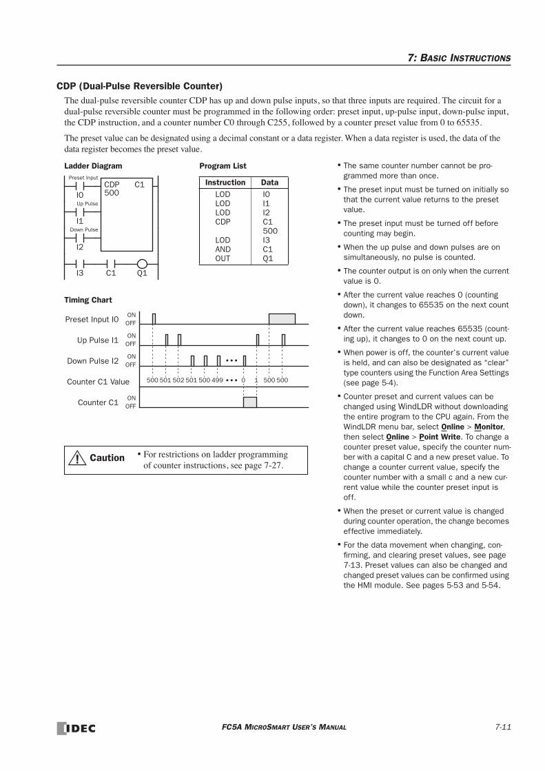
7: BASIC INSTRUCTIONS
CDP (Dual-Pulse Reversible Counter)The dual-pulse reversible counter CDP has up and down pulse inputs, so that three inputs are required. The circuit for a dual-pulse reversible counter must be programmed in the following order: preset input, up-pulse input, down-pulse input, the CDP instruction, and a counter number C0 through C255, followed by a counter preset value from 0 to 65535.
The preset value can be designated using a decimal constant or a data register. When a data register is used, the data of the data register becomes the preset value.
Caution
500 500
Ladder Diagram
Preset Input I0ON
OFF
Up Pulse I1ON
OFF
Down Pulse I2ON
OFF
Timing Chart
Counter C1ON
OFF
500 501 502 501Counter C1 Value 500 499 0 1
• • •
• • •
I0
I1
CDP C1500
I2
Preset Input
Up Pulse
Down Pulse
I3 C1
Instruction DataLODLODLODCDP
LODANDOUT
I0I1I2C1500I3C1Q1
Program List • The same counter number cannot be pro-grammed more than once.
• The preset input must be turned on initially so that the current value returns to the preset value.
• The preset input must be turned off before counting may begin.
• When the up pulse and down pulses are on simultaneously, no pulse is counted.
• The counter output is on only when the current value is 0.
• After the current value reaches 0 (counting down), it changes to 65535 on the next count down.
• After the current value reaches 65535 (count-ing up), it changes to 0 on the next count up.
• When power is off, the counter’s current value is held, and can also be designated as “clear” type counters using the Function Area Settings (see page 5-4).
• Counter preset and current values can be changed using WindLDR without downloading the entire program to the CPU again. From the WindLDR menu bar, select Online > Monitor, then select Online > Point Write. To change a counter preset value, specify the counter num-ber with a capital C and a new preset value. To change a counter current value, specify the counter number with a small c and a new cur-rent value while the counter preset input is off.
• When the preset or current value is changed during counter operation, the change becomes effective immediately.
• For the data movement when changing, con-firming, and clearing preset values, see page 7-13. Preset values can also be changed and changed preset values can be confirmed using the HMI module. See pages 5-53 and 5-54.
Q1
• For restrictions on ladder programming of counter instructions, see page 7-27.
FC5A MICROSMART USER’S MANUAL 7-11

7: BASIC INSTRUCTIONS
CUD (Up/Down Selection Reversible Counter)The up/down selection reversible counter CUD has a selection input to switch the up/down gate, so that three inputs are required. The circuit for an up/down selection reversible counter must be programmed in the following order: preset input, pulse input, up/down selection input, the CUD instruction, and a counter number C0 through C255, followed by a counter preset value from 0 to 65535.
The preset value can be designated using a decimal constant or a data register. When a data register is used, the data of the data register becomes the preset value.
Caution
Ladder Diagram
I0
I1
CUD C2500
I2
Preset Input
Pulse Input
U/D Selection
I3 C2
Instruction DataLODLODLODCUD
LODANDOUT
I0I1I2C2500I3C2Q2
Program List • The same counter number cannot be pro-grammed more than once.
• The preset input must be turned on initially so that the current value returns to the preset value.
• The preset input must be turned off before counting may begin.
• The up mode is selected when the up/down selection input is on.
• The down mode is selected when the up/down selection input is off.
• The counter output is on only when the current value is 0.
• After the current value reaches 0 (counting down), it changes to 65535 on the next count down.
• After the current value reaches 65535 (count-ing up), it changes to 0 on the next count up.
• When power is off, the counter’s current value is held, and can also be designated as “clear” type counters using the Function Area Settings (see page 5-4).
• Counter preset and current values can be changed using WindLDR without downloading the entire program to the CPU again. From the WindLDR menu bar, select Online > Monitor, then select Online > Point Write. To change a counter preset value, specify the counter num-ber with a capital C and a new preset value. To change a counter current value, specify the counter number with a small c and a new cur-rent value while the counter preset input is off.
• When the preset or current value is changed during counter operation, the change becomes effective immediately.
• For the data movement when changing, con-firming, and clearing preset values, see page 7-13. Preset values can also be changed and changed preset values can be confirmed using the HMI module. See pages 5-53 and 5-54.
500 500
Preset Input I0ONOFF
Pulse Input I1ONOFF
U/D Selection ONOFF
Timing Chart
Counter C2ON
OFF
500 501 502 501Counter C2 Value 500 499 0 1
• • •
• • •
Q2
Valid Pulse InputsThe reset or preset input has priority over the pulse input. One scan after the reset or preset input has changed from on to off, the counter starts counting the pulse inputs as they change from off to on.
Reset/PresetON
OFF
PulseON
OFF
More than one scan time is required.
ValidInvalidValid
Input I2
• For restrictions on ladder programming of counter instructions, see page 7-27.
7-12 FC5A MICROSMART USER’S MANUAL
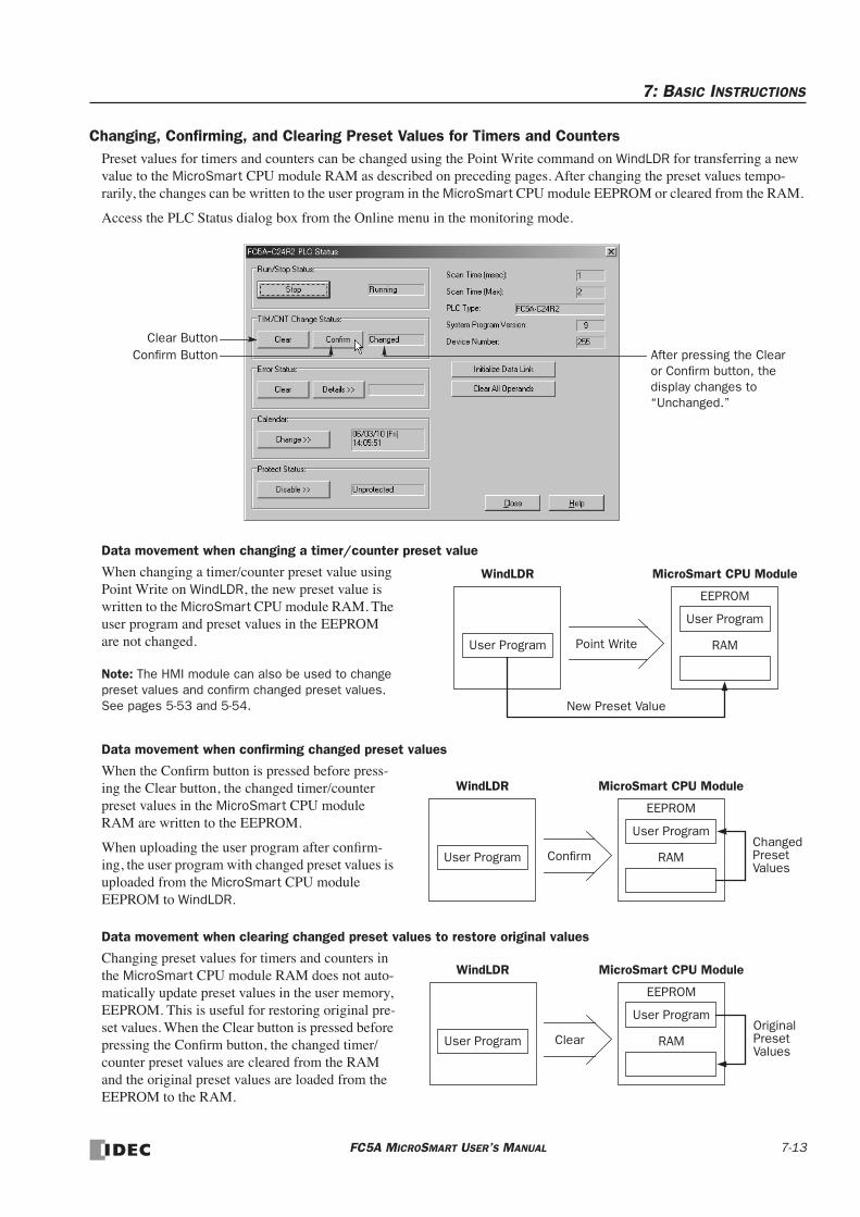
7: BASIC INSTRUCTIONS
Changing, Confirming, and Clearing Preset Values for Timers and CountersPreset values for timers and counters can be changed using the Point Write command on WindLDR for transferring a new value to the MicroSmart CPU module RAM as described on preceding pages. After changing the preset values tempo-rarily, the changes can be written to the user program in the MicroSmart CPU module EEPROM or cleared from the RAM.
Access the PLC Status dialog box from the Online menu in the monitoring mode.
Data movement when changing a timer/counter preset value
When changing a timer/counter preset value using Point Write on WindLDR, the new preset value is written to the MicroSmart CPU module RAM. The user program and preset values in the EEPROM are not changed.
Note: The HMI module can also be used to change preset values and confirm changed preset values. See pages 5-53 and 5-54.
Data movement when confirming changed preset values
When the Confirm button is pressed before press-ing the Clear button, the changed timer/counter preset values in the MicroSmart CPU module RAM are written to the EEPROM.
When uploading the user program after confirm-ing, the user program with changed preset values is uploaded from the MicroSmart CPU module EEPROM to WindLDR.
Data movement when clearing changed preset values to restore original values
Changing preset values for timers and counters in the MicroSmart CPU module RAM does not auto-matically update preset values in the user memory, EEPROM. This is useful for restoring original pre-set values. When the Clear button is pressed before pressing the Confirm button, the changed timer/counter preset values are cleared from the RAM and the original preset values are loaded from the EEPROM to the RAM.
Confirm Button After pressing the Clear or Confirm button, the display changes to “Unchanged.”
Clear Button
WindLDR MicroSmart CPU Module
User Program
EEPROM
RAMUser Program Point Write
New Preset Value
WindLDR MicroSmart CPU Module
Confirm
User Program
EEPROM
RAMUser ProgramChangedPresetValues
WindLDR MicroSmart CPU Module
Clear
User Program
EEPROM
RAMUser ProgramOriginalPresetValues
FC5A MICROSMART USER’S MANUAL 7-13

7: BASIC INSTRUCTIONS
CC= and CC≥ (Counter Comparison)The CC= instruction is an equivalent comparison instruction for counter current values. This instruction will constantly compare current values to the value that has been programmed in. When the counter value equals the given value, the desired output will be initiated.
The CC≥ instruction is an equal to or greater than comparison instruction for counter current values. This instruction will constantly compare current values to the value that has been programmed in. When the counter value is equal to or greater than the given value, the desired output will be initiated.
When a counter comparison instruction is programmed, two addresses are required. The circuit for a counter comparison instruction must be programmed in the following order: the CC= or CC≥ instruction; a counter number C0 through C255, followed by a preset value to compare from 0 to 65535.
The preset value can be designated using a decimal constant or a data register D0 through D1999 (all CPU modules) or D2000 through D7999 and D10000 through D49999 (slim type CPU modules). When a data register is used, the data of the data register becomes the preset value.
• The CC= and CC≥ instructions can be used repeatedly for different preset values.
• The comparison instructions only compare the current value. The status of the counter does not affect this function.
• The comparison instructions also serve as an implicit LOD instruction.
• The comparison instructions can be used with internal relays, which are ANDed or ORed at a separate program address.
• Like the LOD instruction, the comparison instructions can be followed by the AND and OR instructions.
Ladder Diagram (CC=)
Ladder Diagram (CC≥)
Counter # to compare with
Preset value to compare
CC=10
C2
CC>=D15
C3
Instruction DataCC=
OUT
C210Q0
Program List
Instruction DataCC>=
OUT
C3D15Q1
Program List
Q0
Q1
Ladder Diagram
Instruction DataCC=
OUTLODANDOUT
C510M0I0M0Q0
Program List
Ladder Diagram
Instruction DataCC=
ANDOUT
C510I0Q0
Program List
Instruction DataCC=
OROUT
C510I0Q0
Program List
Ladder Diagram
I0I0 M0
CC=10
C5 CC=10
C5I0
CC=10
C5
Q0
M0 Q0 Q0
7-14 FC5A MICROSMART USER’S MANUAL

7: BASIC INSTRUCTIONS
Examples: CC= and CC≥ (Counter Comparison)
Ladder Diagram 1
Timing Chart
CC=5
C2
CNT C210
I1
Reset
PulseI0
CC>=3
C2
Reset Input I0ON
OFF
Pulse Input I1ON
OFF
C2ON
OFF
Output Q1ON
OFF
1
Output Q0
• • •
2 3 4 5 6
ONOFF
7 8 9 10
Instruction DataLODLODCNT
CC=
OUTCC≥
OUT
I0I1C210C25Q0C23Q1
Program List
Output Q0 is on when counter C2 current value is 5.
Output Q1 is turned on when counter C2 current value reaches 3 and remains on until counter C2 is reset.
Q0
Q1
Ladder Diagram 2
Pulse Input I2ON
OFF
Output Q0ON
OFF
Timing Chart1
• • •
500 501 5022
Output Q0 is on when counter C30 current value is 500.CC=
500C30
CNT C301000
I2
Reset
PulseI1
Instruction DataLODLODCNT
CC=
OUT
I1I2C301000C30500Q0
Program List
Q0
Ladder Diagram 3
Pulse Input I4ON
OFF
Output Q1ON
OFF
Timing Chart1
• • •
350 351 3522
Output Q1 is turned on when counter C31 current value reaches 350 and remains on until counter C31 is reset.
CC>=350
C31
CNT C31500
I4
Reset
PulseI3
Instruction DataLODLODCNT
CC>=
OUT
I3I4C31500C31350Q1
Program List
Q1
Ladder Diagram 4
Pulse Input I6ON
OFF
≥C20 (100)ON
OFF
Timing Chart100
• • •
150 151 152101
Q2
Output Q2ON
OFF
Output Q3ON
OFF
• • •
Output Q3 is on when counter C20 current value is between 100 and 149.
Instruction DataLODLODCNT
CC>=
OUTCC>=
ANDNOUT
I5I6C20500C20150Q2C20100Q2Q3
Program List
CC>=150
C20
CNT C20500
I6
Reset
Pulse
I5
CC>=100
C20
Q2
Q3
FC5A MICROSMART USER’S MANUAL 7-15

7: BASIC INSTRUCTIONS
DC= and DC≥ (Data Register Comparison)The DC= instruction is an equivalent comparison instruction for data register values. This instruction will constantly com-pare data register values to the value that has been programmed in. When the data register value equals the given value, the desired output will be initiated.
The DC≥ instruction is an equal to or greater than comparison instruction for data register values. This instruction will constantly compare data register values to the value that has been programmed in. When the data register value is equal to or greater than the given value, the desired output will be initiated.
When a data register comparison instruction is programmed, two addresses are required. The circuit for a data register comparison instruction must be programmed in the following order: the DC= or DC≥ instruction, a data register number D0 through D1999 (all CPU modules) or D2000 through D7999 and D10000 through D49999 (slim type CPU modules), followed by a preset value to compare from 0 to 65535.
The preset value can be designated using a decimal constant or a data register D0 through D1999 (all CPU modules) or D2000 through D7999 and D10000 through D49999 (slim type CPU modules). When a data register is used, the data of the data register becomes the preset value.
• The DC= and DC≥ instructions can be used repeatedly for different preset values.
• The comparison instructions also serve as an implicit LOD instruction.
• The comparison instructions can be used with internal relays, which are ANDed or ORed at a separate program address.
• Like the LOD instruction, the comparison instructions can be followed by the AND and OR instructions.
Ladder Diagram (DC=)
Ladder Diagram (DC≥)
Data register # to compare with
Preset value to compare
DC=50
D2
DC>=D15
D3
Instruction DataDC=
OUT
D250Q0
Program List
Instruction DataDC>=
OUT
D3D15Q1
Program List
Q0
Q1
Ladder Diagram
Instruction DataDC=
OUTLODANDOUT
D510M0I0M0Q0
Program List
Ladder Diagram
Instruction DataDC=
ANDOUT
D510I0Q0
Program List
Instruction DataDC=
OROUT
D510I0Q0
Program List
Ladder Diagram
I0I0 M0
DC=10
D5 DC=10
D5I0
DC=10
D5M0
Q0
Q0 Q0
7-16 FC5A MICROSMART USER’S MANUAL
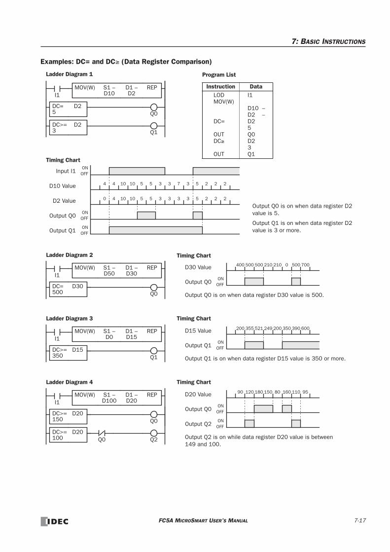
7: BASIC INSTRUCTIONS
Examples: DC= and DC≥ (Data Register Comparison)
Ladder Diagram 1
Timing Chart
DC=5
D2
DC>=3
D2
Input I1ON
OFF
D10 Value
Output Q0ON
OFF
Output Q1ON
OFF
Instruction DataLODMOV(W)
DC=
OUTDC≥
OUT
I1
D10 –D2 –D25Q0D23Q1
Program List
4 4 5 5 3 3 5 210
I1REPS1 –
D10D1 –D2
MOV(W)
10 3 7 2 2
D2 Value 0 4 5 5 3 3 5 210 10 3 3 2 2
Output Q0 is on when data register D2 value is 5.
Output Q1 is on when data register D2 value is 3 or more.
Q0
Q1
Ladder Diagram 2
Output Q0 is on when data register D30 value is 500.
DC=500
D30
Timing Chart
Output Q0ON
OFF
400 210 210 0 500D30 ValueI1
REPS1 –D50
D1 –D30
MOV(W) 500 500 700
Q0
Ladder Diagram 3
DC>=350
D15
I1REPS1 –
D0D1 –D15
MOV(W)
Output Q1 is on when data register D15 value is 350 or more.
Timing Chart
Output Q1ON
OFF
200 249 200 350 390D15 Value 355 521 600
Q1
Ladder Diagram 4
DC>=150
D20
DC>=100
D20Q0
I1REPS1 –
D100D1 –D20
MOV(W)
Output Q2 is on while data register D20 value is between 149 and 100.
Timing Chart
Output Q0ON
OFF
90 150 80 160 110D20 Value 120 180 95
Output Q2ON
OFFQ0
Q2
FC5A MICROSMART USER’S MANUAL 7-17

7: BASIC INSTRUCTIONS
SFR and SFRN (Forward and Reverse Shift Register)All-in-one type CPU modules have a shift register consisting of 128 bits which are allocated to R0 through R127. Slim type CPU modules have a shift register consisting of 256 bits which are allocated to R0 through R255. Any number of available bits can be selected to form a train of bits which store on or off status. The on/off data of constituent bits is shifted in the forward direction (forward shift register) or in the reverse direction (reverse shift register) when a pulse input is turned on.
Forward Shift Register (SFR)When SFR instructions are programmed, two addresses are always required. The SFR instruction is entered, followed by a shift register number selected from appropriate operand numbers. The shift register number corresponds to the first, or head bit. The number of bits is the second required address after the SFR instruction.
The SFR instruction requires three inputs. The forward shift register circuit must be programmed in the following order: reset input, pulse input, data input, and the SFR instruction, followed by the first bit and the number of bits.
Reset InputThe reset input will cause the value of each bit of the shift register to return to zero. Initialize pulse special internal relay, M8120, may be used to initialize the shift register at start-up.
Pulse InputThe pulse input triggers the data to shift. The shift is in the forward direction for a forward shift register and in reverse for a reverse shift register. A data shift will occur upon the leading edge of a pulse; that is, when the pulse turns on. If the pulse has been on and stays on, no data shift will occur.
Data InputThe data input is the information which is shifted into the first bit when a forward data shift occurs, or into the last bit when a reverse data shift occurs.
Note: When power is turned off, the statuses of all shift register bits are normally cleared. It is also possible to maintain the statuses of shift register bits by using the Function Area Settings as required. See page 5-4.
Ladder Diagram
Structural Diagram
I2
I0
R0
Reset
Data
I1
Pulse
R1 R2 R3
Shift Direction
First Bit: R0 # of Bits: 4
I0
I1
SFR R04
I2
Reset
Pulse
Data
Instruction DataLODLODLODSFR
I0I1I2R04
Program ListFirst Bit
# of Bits
Structural Diagram
I2
I0
R0
Reset
Data
I1
Pulse
R1 R2 R3
Shift Direction
# of Bits: 4
CPU Type All-in-One CPU Slim CPUFirst Bit R0 to R127 R0 to R255# of Bits 1 to 128 1 to 256
Caution • For restrictions on ladder programming of shift register instructions, see page 7-27.
7-18 FC5A MICROSMART USER’S MANUAL
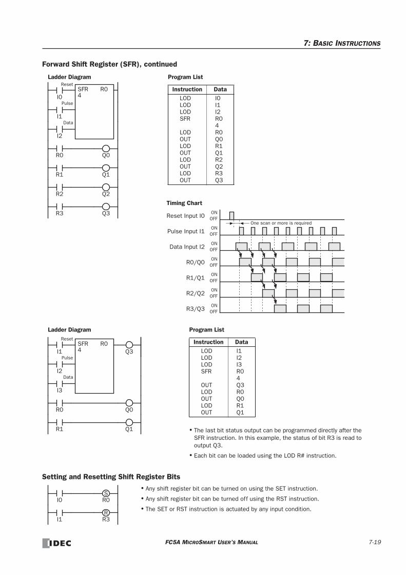
7: BASIC INSTRUCTIONS
Forward Shift Register (SFR), continued
Setting and Resetting Shift Register Bits
Reset Input I0ON
OFF
Pulse Input I1ON
OFF
Data Input I2ON
OFF
Timing Chart
R1/Q1ON
OFF
One scan or more is required
R0/Q0ON
OFF
R3/Q3ON
OFF
R2/Q2ON
OFF
Ladder Diagram
I0
I1
SFR R04
I2
Reset
Pulse
Data
R0
R1
R2
R3
Instruction DataLODLODLODSFR
LODOUTLODOUTLODOUTLODOUT
I0I1I2R04R0Q0R1Q1R2Q2R3Q3
Program List
Q0
Q1
Q2
Q3
• The last bit status output can be programmed directly after the SFR instruction. In this example, the status of bit R3 is read to output Q3.
• Each bit can be loaded using the LOD R# instruction.
Instruction DataLODLODLODSFR
OUTLODOUTLODOUT
I1I2I3R04Q3R0Q0R1Q1
Program ListLadder Diagram
I1
I2
SFR R04
I3
Reset
Pulse
Data
R0
R1
Q0
Q1
Q3
I1
I0
• Any shift register bit can be turned on using the SET instruction.
• Any shift register bit can be turned off using the RST instruction.
• The SET or RST instruction is actuated by any input condition.
R0S
R3R
FC5A MICROSMART USER’S MANUAL 7-19

7: BASIC INSTRUCTIONS
Reverse Shift Register (SFRN)For reverse shifting, use the SFRN instruction. When SFRN instructions are programmed, two addresses are always required. The SFRN instructions are entered, followed by a shift register number selected from appropriate operand num-bers. The shift register number corresponds to the lowest bit number in a string. The number of bits is the second required address after the SFRN instructions.
The SFRN instruction requires three inputs. The reverse shift register circuit must be programmed in the following order: reset input, pulse input, data input, and the SFRN instruction, followed by the last bit and the number of bits.
Structural Diagram
I2
I0
R20
Reset
Data
I1
Pulse
R21 R22 R23
Shift Direction
Last Bit: R20 # of Bits: 7
R24 R25 R26
Note: Output is initiated only for those bits highlighted in bold print.
Note: When power is turned off, the statuses of all shift register bits are normally cleared. It is also possible to maintain the statuses of shift register bits by using the Function Area Settings as required. See page 5-4.
• The last bit status output can be programmed directly after the SFRN instruction. In this example, the status of bit R20 is read to output Q0.
• Each bit can be loaded using the LOD R# instructions.
• For details of reset, pulse, and data inputs, see page 7-18.
Ladder Diagram
I0
I1
SFRN R207
I2
Reset
Pulse
Data
R21
Last Bit
# of Bits
R23
R25
Instruction DataLODLODLODSFRN
OUTLODOUTLODOUTLODOUT
I0I1I2R207Q0R21Q1R23Q2R25Q3
Program List
Q0
Q1
Q3
Q2
CPU Type All-in-One CPU Slim CPULast Bit R0 to R127 R0 to R255# of Bits 1 to 128 1 to 256
Caution • For restrictions on ladder programming of shift register instructions, see page 7-27.
7-20 FC5A MICROSMART USER’S MANUAL

7: BASIC INSTRUCTIONS
Bidirectional Shift RegisterA bidirectional shift register can be created by first programming the SFR instruction as detailed in the Forward Shift Reg-ister section on page 7-18. Next, the SFRN instruction is programed as detailed in the Reverse Shift Register section on page 7-20.
Structural Diagram
I3
I1
R22
Reset
Data
I2
Pulse
R23 R24 R25
Forward Shifting
Last Bit: R22 # of Bits: 6
R26 R27
Note: Output is initiated only for those bits highlighted in bold print.
I4
I6
I5
Reset
Data
Pulse
First Bit: R22 # of Bits: 6
Reverse Shifting
Ladder Diagram
I1
I2
SFR R226
I3
Reset
Pulse
Data
I4
I5
SFRN R226
I6
Reset
Pulse
Data
R23
R24
R26
Instruction DataLODLODLODSFR
LODLODLODSFRN
LODOUTLODOUTLODOUT
I1I2I3R226I4I5I6R226R23Q0R24Q1R26Q2
Program List
Q0
Q2
Q1
FC5A MICROSMART USER’S MANUAL 7-21

7: BASIC INSTRUCTIONS
SOTU and SOTD (Single Output Up and Down)The SOTU instruction “looks for” the transition of a given input from off to on. The SOTD instruction looks for the transi-tion of a given input from on to off. When this transition occurs, the desired output will turn on for the length of one scan. The SOTU or SOTD instruction converts an input signal to a “one-shot” pulse signal.
A total of 3072 SOTU and SOTD instructions can be used in a user program.
If operation is started while the given input is already on, the SOTU output will not turn on. The transition from off to on is what triggers the SOTU instruction.
When a relay of the CPU or relay output module is defined as the SOTU or SOTD output, it may not operate if the scan time is not compatible with relay requirements.
There is a special case when the SOTU and SOTD instructions are used between the MCS and MCR instructions (which are detailed on page 7-23). If input I2 to the SOTU instruction turns on while input I1 to the MCS instruction is on, then the SOTU output turns on. If input I2 to the SOTD instruction turns off while input I1 is on, then the SOTD output turns on. If input I1 turns on while input I2 is on, then the SOTU output turns on. However, if input I1 turns off while input I2 is on, then the SOTD output does not turn on as shown below.
Caution
I0
I0
Ladder Diagram
Input I0ONOFF
Output Q0ONOFF
Output Q1ONOFF
Timing Chart
SOTU
SOTD
T
T T
T
Note: “T” equals one scan time (one-shot pulse).
Instruction DataLODSOTUOUTLODSOTDOUT
I0
Q0I0
Q1
Program List
Q0
Q1
• For restrictions on ladder programming of SOTU and SOTD instructions, see page 7-27.
I2
I1
Ladder Diagram
Input I1ON
OFF
SOTU Output M1ON
OFF
SOTD Output M2ON
OFF
Timing Chart
MCS
SOTD
MCRNo Output No Output
I2SOTU
Input I2ON
OFF
M1
M2
7-22 FC5A MICROSMART USER’S MANUAL

7: BASIC INSTRUCTIONS
MCS and MCR (Master Control Set and Reset)The MCS (master control set) instruction is usually used in combination with the MCR (master control reset) instruction. The MCS instruction can also be used with the END instruction, instead of the MCR instruction.
When the input preceding the MCS instruction is off, the MCS is executed so that all inputs to the portion between the MCS and the MCR are forced off. When the input preceding the MCS instruction is on, the MCS is not executed so that the program following it is executed according to the actual input statuses.
When the input condition to the MCS instruction is off and the MCS is executed, other instructions between the MCS and MCR are executed as follows:
Input conditions cannot be set for the MCR instruction.
More than one MCS instruction can be used with one MCR instruction.
Corresponding MCS/MCR instructions cannot be nested within another pair of corresponding MCS/MCR instructions.
Instruction Status
SOTU Rising edges (ON pulses) are not detected.
SOTD Falling edges (OFF pulses) are not detected.
OUT All are turned off.
OUTN All are turned on.
SET and RST All are held in current status.
TML, TIM, TMH, and TMSCurrent values are reset to zero.Timeout statuses are turned off.
CNT, CDP, and CUDCurrent values are held.Pulse inputs are turned off.Countout statuses are turned off.
SFR and SFRNShift register bit statuses are held.Pulse inputs are turned off.The output from the last bit is turned off.
Ladder Diagram
I0
I1
Input I0ONOFF
Input I1ONOFF
Output Q0ONOFF
Timing Chart
MCS
MCR
When input I0 is off, MCS is executed so that the subsequent input is forced off.
When input I0 is on, MCS is not executed so that the following program is executed according to the actual input statuses.
Instruction DataLODMCSLODOUTMCR
I0
I1Q0
Program List
Q0
FC5A MICROSMART USER’S MANUAL 7-23
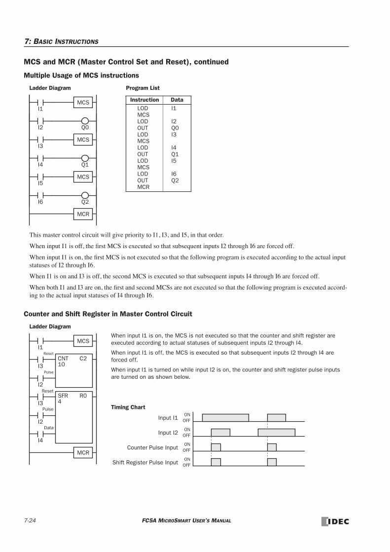
7: BASIC INSTRUCTIONS
MCS and MCR (Master Control Set and Reset), continued
Multiple Usage of MCS instructions
Counter and Shift Register in Master Control Circuit
Ladder Diagram
I1
I2
I3
I4
I5
I6
MCS
MCR
MCS
MCS
This master control circuit will give priority to I1, I3, and I5, in that order.
When input I1 is off, the first MCS is executed so that subsequent inputs I2 through I6 are forced off.
When input I1 is on, the first MCS is not executed so that the following program is executed according to the actual input statuses of I2 through I6.
When I1 is on and I3 is off, the second MCS is executed so that subsequent inputs I4 through I6 are forced off.
When both I1 and I3 are on, the first and second MCSs are not executed so that the following program is executed accord-ing to the actual input statuses of I4 through I6.
Instruction DataLODMCSLODOUTLODMCSLODOUTLODMCSLODOUTMCR
I1
I2Q0I3
I4Q1I5
I6Q2
Program List
Q2
Q0
Q1
Ladder Diagram
I1MCS
MCR
Input I1ON
OFF
Counter Pulse InputON
OFF
Shift Register Pulse InputON
OFF
Timing Chart
Input I2ON
OFF
When input I1 is on, the MCS is not executed so that the counter and shift register are executed according to actual statuses of subsequent inputs I2 through I4.
When input I1 is off, the MCS is executed so that subsequent inputs I2 through I4 are forced off.
When input I1 is turned on while input I2 is on, the counter and shift register pulse inputs are turned on as shown below.
CNT C210
I2
Reset
PulseI3
I3
I2
SFR R04
I4
Reset
Pulse
Data
7-24 FC5A MICROSMART USER’S MANUAL

7: BASIC INSTRUCTIONS
JMP (Jump) and JEND (Jump End)The JMP (jump) instruction is usually used in combination with the JEND (jump end) instruction. At the end of a program, the JMP instruction can also be used with the END instruction, instead of the JEND instruction.
These instructions are used to proceed through the portion of the program between the JMP and the JEND without pro-cessing. This is similar to the MCS/MCR instructions, except that the portion of the program between the MCS and MCR instruction is executed.
When the operation result immediately before the JMP instruction is on, the JMP is valid and the program is not executed. When the operation result immediately before the JMP instruction is off, the JMP is invalid and the program is executed.
When the input condition to the JMP instruction is on and the JMP is executed, other instructions between the JMP and JEND are executed as follows:
Input conditions cannot be set for the JEND instruction.
More than one JMP instruction can be used with one JEND instruction.
Corresponding JMP/JEND instructions cannot be nested within another pair of corresponding JMP/JEND instructions.
Instruction Status
SOTU Rising edges (ON pulses) are not detected.
SOTD Falling edges (OFF pulses) are not detected.
OUT and OUTN All are held in current status.
SET and RST All are held in current status.
TML, TIM, TMH, and TMSCurrent values are held.Timeout statuses are held.
CNT, CDP, and CUDCurrent values are held.Pulse inputs are turned off.Countout statuses are held.
SFR and SFRNShift register bit statuses are held.Pulse inputs are turned off.The output from the last bit is held.
Ladder Diagram
I0
I1
Input I0ONOFF
Input I1ONOFF
Output Q0ONOFF
Timing Chart
JMP
JEND
When input I0 is on, JMP is executed so that the subsequent output status is held.
When input I0 is off, JMP is not executed so that the following program is executed according to the actual input statuses.
Instruction DataLODJMPLODOUTJEND
I0
I1Q0
Program List
Q0
FC5A MICROSMART USER’S MANUAL 7-25

7: BASIC INSTRUCTIONS
JMP (Jump) and JEND (Jump End), continued
ENDThe END instruction is always required at the end of a program; however, it is not necessary to program the END instruc-tion after the last programmed instruction. The END instruction already exists at every unused address. (When an address is used for programming, the END instruction is removed.)
A scan is the execution of all instructions from address zero to the END instruction. The time required for this execution is referred to as one scan time. The scan time varies with respect to program length, which corresponds to the address where the END instruction is found.
During the scan time, program instructions are processed sequentially. This is why the output instruction closest to the END instruction has priority over a previous instruction for the same output. No output is initiated until all logic within a scan is processed.
Output occurs simultaneously, and this is the first part of the END instruction execution. The second part of the END instruction execution is to monitor all inputs, also done simultaneously. Then program instructions are ready to be pro-cessed sequentially once again.
Ladder Diagram
I1
I2
I3
I4
I5
I6
JMP
JEND
JMP
JMP
This jump circuit will give priority to I1, I3, and I5, in that order.
When input I1 is on, the first JMP is executed so that subsequent output statuses of Q0 through Q2 are held.
When input I1 is off, the first JMP is not executed so that the following program is executed according to the actual input statuses of I2 through I6.
When I1 is off and I3 is on, the second JMP is executed so that subsequent output statuses of Q1 and Q2 are held.
When both I1 and I3 are off, the first and second JMPs are not executed so that the following program is executed accord-ing to the actual input statuses of I4 through I6.
Instruction DataLODJMPLODOUTLODJMPLODOUTLODJMPLODOUTJEND
I1
I2Q0I3
I4Q1I5
I6Q2
Program List
Q2
Q0
Q1
Ladder Diagram
END
Instruction DataLODOUTLODOUTEND
I0Q0I1Q1
Program List
Q1
I0
I1
Q0
7-26 FC5A MICROSMART USER’S MANUAL

7: BASIC INSTRUCTIONS
Restriction on Ladder ProgrammingDue to the structure of WindLDR, the following ladder diagram cannot be programmed — a closed circuit block is formed by vertical lines, except for right and left power rails, and the closed circuit block contains one or more prohibited instruc-tions shown in the table below.
Modifying Prohibited Ladder ProgramsIntended operation can be performed by modifying the prohibited ladder program as shown in the examples below:
Prohibited Instructions OUT, OUTN, SET, RST, TML, TIM, TMH, TMS, CNT, CDP, CUD, SFR, SFRN, SOTU, SOTD
Error DetectionWhen converting the ladder program, an error message is shown, such as “TIM follows an invalid operand.” Conversion fails to create mnemonics and the program is not downloaded to the CPU module.
ProhibitedInstructionRelay 1
Program
Relay 2
Closed Circuit Block
VerticalLine A
VerticalLine B
Program
Left Power Rail Right Power Rail
M0
Prohibited Ladder Program 1
TIM100
T0Q0M1
M2
M0
Modified Ladder Program 1
TIM100
T0M1
T0M0 Q0
M2
M0
Prohibited Ladder Program 2
TIM100
T0Q0M1
M2
M0
Modified Ladder Program 2
TIM100
T0M1
T0 Q0
TIM50
T1 TIM50
T1M2
T1
FC5A MICROSMART USER’S MANUAL 7-27

7: BASIC INSTRUCTIONS
7-28 FC5A MICROSMART USER’S MANUAL

8: ADVANCED INSTRUCTIONS
IntroductionThis chapter describes general rules of using advanced instructions, terms, data types, and formats used for advanced instructions.
Advanced Instruction List
Group Symbol NameValid Data Type
See PageW I D L F
NOP NOP No Operation 8-8
Move
MOV Move X X X X 9-1MOVN Move Not X X X X 9-5IMOV Indirect Move X X 9-6IMOVN Indirect Move Not X X 9-7BMOV Block Move X 9-8IBMV Indirect Bit Move X 9-9IBMVN Indirect Bit Move Not X 9-11
Data Comparison
CMP= Compare Equal To X X X X X 10-1CMP<> Compare Unequal To X X X X X 10-1CMP< Compare Less Than X X X X X 10-1CMP> Compare Greater Than X X X X X 10-1CMP<= Compare Less Than or Equal To X X X X X 10-1CMP>= Compare Greater Than or Equal To X X X X X 10-1ICMP>= Interval Compare Greater Than or Equal To X X X X X 10-5
Binary Arithmetic
ADD Addition X X X X X 11-1SUB Subtraction X X X X X 11-1MUL Multiplication X X X X X 11-1DIV Division X X X X X 11-1ROOT Root X X X 11-13
Boolean ComputationANDW AND Word X X 12-1ORW OR Word X X 12-1XORW Exclusive OR Word X X 12-1
Shift and Rotate
SFTL Shift Left 13-1SFTR Shift Right 13-3BCDLS BCD Left Shift X 13-5WSFT Word Shift X 13-7ROTL Rotate Left X X 13-8ROTR Rotate Right X X 13-10
Data Conversion
HTOB Hex to BCD X X 14-1BTOH BCD to Hex X X 14-3HTOA Hex to ASCII X 14-5ATOH ASCII to Hex X 14-7BTOA BCD to ASCII X 14-9ATOB ASCII to BCD X 14-11ENCO Encode 14-13DECO Decode 14-14BCNT Bit Count 14-15ALT Alternate Output 14-16CVDT Convert Data Type X X X X X 14-17
Week ProgrammerWKTIM Week Timer 15-1WKTBL Week Table 15-2
FC5A MICROSMART USER’S MANUAL 8-1
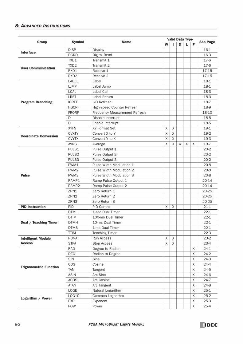
8: ADVANCED INSTRUCTIONS
InterfaceDISP Display 16-1DGRD Digital Read 16-3
User Communication
TXD1 Transmit 1 17-6TXD2 Transmit 2 17-6RXD1 Receive 1 17-15RXD2 Receive 2 17-15
Program Branching
LABEL Label 18-1LJMP Label Jump 18-1LCAL Label Call 18-3LRET Label Return 18-3IOREF I/O Refresh 18-7HSCRF High-speed Counter Refresh 18-9FRQRF Frequency Measurement Refresh 18-10DI Disable Interrupt 18-5EI Enable Interrupt 18-5
Coordinate Conversion
XYFS XY Format Set X X 19-1CVXTY Convert X to Y X X 19-2CVYTX Convert Y to X X X 19-3AVRG Average X X X X X 19-7
Pulse
PULS1 Pulse Output 1 20-2PULS2 Pulse Output 2 20-2PULS3 Pulse Output 3 20-2PWM1 Pulse Width Modulation 1 20-8PWM2 Pulse Width Modulation 2 20-8PWM3 Pulse Width Modulation 3 20-8RAMP1 Ramp Pulse Output 1 20-14RAMP2 Ramp Pulse Output 2 20-14ZRN1 Zero Return 1 20-25ZRN2 Zero Return 2 20-25ZRN3 Zero Return 3 20-25
PID Instruction PID PID Control X X 21-1
Dual / Teaching Timer
DTML 1-sec Dual Timer 22-1DTIM 100-ms Dual Timer 22-1DTMH 10-ms Dual Timer 22-1DTMS 1-ms Dual Timer 22-1TTIM Teaching Timer 22-3
Intelligent Module Access
RUNA Run Access X X 23-2STPA Stop Access X X 23-4
Trigonometric Function
RAD Degree to Radian X 24-1DEG Radian to Degree X 24-2SIN Sine X 24-3COS Cosine X 24-4TAN Tangent X 24-5ASIN Arc Sine X 24-6ACOS Arc Cosine X 24-7ATAN Arc Tangent X 24-8
Logarithm / Power
LOGE Natural Logarithm X 25-1LOG10 Common Logarithm X 25-2EXP Exponent X 25-3POW Power X 25-4
Group Symbol NameValid Data Type
See PageW I D L F
8-2 FC5A MICROSMART USER’S MANUAL

8: ADVANCED INSTRUCTIONS
Advanced Instruction Applicable CPU ModulesApplicable advanced instructions depends on the type of CPU modules as listed in the table below.
Group SymbolAll-in-One Type CPU Modules Slim Type CPU Modules
FC5A-C10R2 FC5A-C10R2C
FC5A-C16R2 FC5A-C16R2C
FC5A-C24R2FC5A-C24R2C
FC5A-D16RK1 FC5A-D16RS1
FC5A-D32K3 FC5A-D32S3
NOP NOP X X X X X
Move
MOV X X X X XMOVN X X X X XIMOV X X X X XIMOVN X X X X XBMOV X X X X XIBMV X X X X XIBMVN X X X X X
Data Comparison
CMP= X X X X XCMP<> X X X X XCMP< X X X X XCMP> X X X X XCMP<= X X X X XCMP>= X X X X XICMP>= X X X X X
Binary Arithmetic
ADD X X X X XSUB X X X X XMUL X X X X XDIV X X X X XROOT X X X X X
Boolean Computation
ANDW X X X X XORW X X X X XXORW X X X X X
Shift and Rotate
SFTL X X X X XSFTR X X X X XBCDLS X X X X XWSFT X X X X XROTL X X X X XROTR X X X X X
Data Conversion
HTOB X X X X XBTOH X X X X XHTOA X X X X XATOH X X X X XBTOA X X X X XATOB X X X X XENCO X X X X XDECO X X X X XBCNT X X X X XALT X X X X XCVDT X X X X X
Week Programmer
WKTIM X X X X XWKTBL X X X X X
InterfaceDISP X X XDGRD X X X
FC5A MICROSMART USER’S MANUAL 8-3

8: ADVANCED INSTRUCTIONS
User Communication
TXD1 X X X X XTXD2 X X X X XRXD1 X X X X XRXD2 X X X X X
Program Branching
LABEL X X X X XLJMP X X X X XLCAL X X X X XLRET X X X X XIOREF X X X X XHSCRF X X X X XFRQRF X X X X XDI X X X X XEI X X X X X
Coordinate Conversion
XYFS X X X X XCVXTY X X X X XCVYTX X X X X XAVRG X X X X X
Pulse
PULS1 X XPULS2 X XPULS3 XPWM1 X XPWM2 X XPWM3 XRAMP1 X XRAMP2 XZRN1 X XZRN2 X XZRN3 X
PID Instruction PID X X X
Dual / Teaching Timer
DTML X X X X XDTIM X X X X XDTMH X X X X XDTMS X X X X XTTIM X X X X X
Intelligent Module Access
RUNA X X XSTPA X X X
Trigonometric Function
RAD X X X X XDEG X X X X XSIN X X X X XCOS X X X X XTAN X X X X XASIN X X X X XACOS X X X X XATAN X X X X X
Logarithm / Power
LOGE X X X X XLOG10 X X X X XEXP X X X X XPOW X X X X X
Group SymbolAll-in-One Type CPU Modules Slim Type CPU Modules
FC5A-C10R2 FC5A-C10R2C
FC5A-C16R2 FC5A-C16R2C
FC5A-C24R2FC5A-C24R2C
FC5A-D16RK1 FC5A-D16RS1
FC5A-D32K3 FC5A-D32S3
8-4 FC5A MICROSMART USER’S MANUAL

8: ADVANCED INSTRUCTIONS
Structure of an Advanced Instruction
Input Condition for Advanced InstructionsAlmost all advanced instructions must be preceded by a contact, except NOP (no operation), LABEL (label), LRET (label return), STPA (stop access) instructions. The input condition can be programmed using a bit operand such as input, output, internal relay, or shift register. Timer and counter can also be used as an input condition to turn on the contact when the timer times out or the counter counts out.
While the input condition is on, the advanced instruction is executed in each scan. To execute the advanced instruction only at the rising or falling edge of the input, use the SOTU or SOTD instruction.
While the input condition is off, the advanced instruction is not executed and operand statuses are held.
Source and Destination OperandsThe source and destination operands specify 16- or 32-bit data, depending on the selected data type. When a bit operand such as input, output, internal relay, or shift register is designated as a source or destination operand, 16 or 32 points start-ing with the designated number are processed as source or destination data. When a word operand such as timer or counter is designated as a source operand, the current value is read as source data. When a timer or counter is designated as a des-tination operand, the result of the advanced instruction is set to the preset value for the timer or counter. When a data reg-ister is designated as a source or destination operand, the data is read from or written to the designated data register.
Using Timer or Counter as Source OperandSince all timer instructions — TML (1-sec timer), TIM (100-ms timer), TMH (10-ms timer), and TMS (1-ms timer) —
subtract from the preset value, the current value is decremented from the preset value and indicates the remaining time. As described above, when a timer is designated as a source operand of an advanced instruction, the current value, or the remaining time, of the timer is read as source data. Adding counters CNT start counting at 0, and the current value is incre-mented up to the preset value. Reversible counters CDP and CUD start counting at the preset value and the current value is incremented or decremented from the preset value. When any counter is designated as a source operand of an advanced instruction, the current value is read as source data.
Using Timer or Counter as Destination OperandAs described above, when a timer or counter is designated as a destination operand of an advanced instruction, the result of the advanced instruction is set to the preset value of the timer or counter. Timer and counter preset values can be 0 through 65535.
When a timer or counter preset value is designated using a data register, the timer or counter cannot be designated as a des-tination of an advanced instruction. When executing such an advanced instruction, a user program execution error will result. For details of user program execution error, see page 32-6.
Note: When a user program execution error occurs, the result is not set to the destination.
Repeat DesignationSpecifies whether repeat is used for the operand or not.
Repeat CyclesSpecifies the quantity of repeat cycles: 1 through 99.
I0S1 R
*****REP**
D1 R*****
OpcodeThe opcode is a symbol to identify the advanced instruction.
Data TypeSpecifies the word (W), integer (I), double word (D), long (L), or float (F) data type.
Source OperandThe source operand specifies the 16- or 32-bit data to be processed by the advanced instruction. Some advanced instructions require two source operands.
Destination OperandThe destination operand specifies the 16- or 32-bit data to store the result of the advanced instruction. Some advanced instructions require two destination operands.
Opcode
Source Operand
Repeat Cycles
Destination Operand
Repeat
MOV(W)
Data TypeDesignation
I0REPS1 –
D10D1 –D20
SOTU MOV(W)
FC5A MICROSMAR
T USER’S MANUAL 8-5
8: ADVANCED INSTRUCTIONS
Data Types for Advanced Instructions (Integer Type)When using move, data comparison, binary arithmetic, Boolean computation, bit shift/rotate, data conversion, and coordi-nate conversion instructions, data types can be selected from word (W), integer (I), double word (D), long (L), or float (F). For other advanced instructions, the data is processed in units of 16-bit word.
Decimal Values and Hexadecimal Storage (Word, Integer, Double, and Long Data Types)The following table shows hexadecimal equivalents which are stored in the CPU, as a result of addition and subtraction of the decimal values shown:
Data Type Symbol BitsQuantity of Data Registers Used
Range of Decimal Values
Word (Unsigned 16 bits) W 16 bits 1 0 to 65,535
Integer (Signed 15 bits) I 16 bits 1 –32,768 to 32,767
Double Word (Unsigned 32 bits) D 32 bits 2 0 to 4,294,967,295
Long (Signed 31 bits) L 32 bits 2 –2,147,483,648 to 2,147,483,647
Float (Floating point) F 32 bits 2 –3.402823×1038 to 3.402823×1038
Data Type Result of Addition Hexadecimal Storage Result of Subtraction Hexadecimal Storage
Word
065535131071
0000FFFF
(CY) FFFF
655350–1
–65535–65536
FFFF0000
(BW) FFFF(BW) 0001(BW) 0000
Integer
655343276832767
0–1
–32767–32768–32769–65535
(CY) 7FFE(CY) 0000
7FFF0000FFFF80018000
(CY) FFFF(CY) 8001
655343276832767
0–1
–32767–32768–32769–65535
(BW) 7FFE(BW) 0000
7FFF0000FFFF80018000
(BW) FFFF(BW) 8001
Double Word
042949672958589934591
00000000FFFFFFFF
(CY) FFFFFFFF
42949672950–1
–4294967295–4294967296
FFFFFFFF00000000
(BW) FFFFFFFF(BW) 00000001(BW) 00000000
Long
429496729421474836482147483647
0–1
–2147483647–2147483648–2147483649–4294967295
(CY) 7FFFFFFE(CY) 00000000
7FFFFFFF00000000FFFFFFFF
8000000180000000
(CY) FFFFFFFF(CY) 80000001
429496729421474836482147483647
0–1
–2147483647–2147483648–2147483649–4294967295
(BW) 7FFFFFFE(BW) 00000000
7FFFFFFF00000000FFFFFFFF
8000000180000000
(BW) FFFFFFFF(BW) 80000001
8-6 FC5A MICROSMART USER’S MANUAL

8: ADVANCED INSTRUCTIONS
Floating-Point Data FormatThe FC5A MicroSmart can specify the floating-point data type (F) for advanced instructions. Like the double word (D) and long integer (L) data types, the floating-point data type also uses two consecutive data registers to execute advanced instructions. The FC5A MicroSmart supports the floating-point data based on the single storage format of the IEEE (The Institute of Electrical and Electronics Engineers) Standard 754.
Single Storage FormatThe IEEE single format consists of three fields: a 23-bit fraction, f; an 8-bit biased exponent, e; and 1-bit sign, s. These fields are stored contiguously in one 32-bit word, as shown in the figure below. Bits 0:22 contain the 23-bit fraction, f, with bit 0 being the least significant bit of the fraction and bit 22 being the most significant; bits 23:30 contain the 8-bit biased exponent, e, with bit 23 being the least significant bit of the biased exponent and bit 30 being the most significant; and the highest-order bit 31 contains the sign bit, s.
The table below shows the correspondence between the values of the three constituent fields s, e, and f and the value repre-sented by the single format bit pattern. When any value out of the bit pattern is entered to the advanced instruction or when execution of advanced instructions, such as division by zero, has produced any value out of the bit pattern, a user program execution error will result, turning on special internal relay M8004 and the ERR LED on the CPU module.
Carry and Borrow in Floating-Point Data ProcessingWhen advanced instructions involving floating-point data are executed, special internal relay M8003 (carry and borrow) is updated.
Single Format Bit Patters Value
0 < e < 255 (–1)s × 2e–127 × 1.f (normal numbers)
e = 0; f = 0 (all bits in f are zero) (–1)s × 2e–127 × 0.0 (signed zero)
M8003 Execution Result Value
1 ≠ 0 Overflow (out of the range between –3.402823×1038 and 3.402823×1038)
1 0 Not zero (within the range between –1.175495×10–38 and 1.175495×10–38)
0 0 Zero
s e[30:23] f[22:0]
31 30 23 22 0
Single Storage Format
23-bit fraction8-bit biased exponent
Sign bit (0: positive, 1: negative)
0
–1.175495×10–38
M8003 1 1
1.175495×10–380–3.402823×1038
0
Execution Result
1
Overflow
0 1
3.402823×1038
OverflowNot Zero
FC5A MICROSMART USER’S MANUAL 8-7

8: ADVANCED INSTRUCTIONS
Double-word Operands in Data RegistersWhen the double-word data type is selected for the source or destination operand, the data is loaded from or stored to two consecutive data registers. The order of the two operands depends on the operand type.
When a data register, timer, or counter is selected as a double-word operand, the high-word data is loaded from or stored to the first operand selected. The low-word data is loaded from or stored to the subsequent operand.
Example: When data register D10 is designated as a double-word source operand and data register D20 is designated as a double-word destination operand, the data is loaded from or stored to two consecutive data registers as illustrated below.
Discontinuity of Operand AreasEach operand area is discrete and does not continue, for example, from input to output or from output to internal relay. In addition, special internal relays M8000 through M8157 (all-in-one type CPU) or M8317 (slim type CPU) are in a separate area from internal relays M0 through M2557. Data registers D0 through D1999, expansion data registers D2000 through D7999 (slim type CPU only), and special data registers D8000 through D8199 (all-in-one type CPU) or D8499 (slim type CPU) are in separate areas and do not continue with each other.
Advanced instructions execute operation only on the available operands in the valid area. If a user program syntax error is found during programming, WindLDR rejects the program instruction and shows an error message.
NOP (No Operation)
Details of all other advanced instructions are described in the following chapters.
305419896
Double-word Data
High Word D10
(12345678h)
Source Operand
4660(1234h)
Low Word D11 22136(5678h)
High Word D204660(1234h)
Low Word D2122136(5678h)
Destination Operand
The internal relay ends at M2557. Since the MOV (move) instruction reads 16 internal relays, the last internal relay exceeds the valid range, resulting in a user program syntax error.M8125
REPS1 –M2550
D1 –D0
MOV(W)
This program results in a user program syntax error. The destina-tion of the DIV (division) instruction requires two data registers D1999 and D2000. Since D2000 exceeds the valid range, a user program syntax error occurs.
I0REPS1 –
D100S2 –D200
DIV(W) D1 –D1999
The MOV (move) instruction sets data of data register D0 to 16 outputs Q610 through Q627 in the first repeat cycle. The destination of the sec-ond cycle is the next 16 outputs Q630 through Q647, which are invalid, resulting in a user program syntax error.
For details about repeat operations of each advanced instruction, see the following chapters.
M8125REP2
S1 –D0
D1 RQ610
MOV(W)
No operation is executed by the NOP instruction.
The NOP instruction may serve as a place holder. Another use would be to add a delay to the CPU scan time, in order to simulate communication with a machine or application, for debugging purposes.
The NOP instruction does not require an input and operand.
NOP
8-8 FC5A MICROSMART USER’S MANUAL

9: MOVE INSTRUCTIONS
IntroductionData can be moved using the MOV (move), MOVN (move not), IMOV (indirect move), or IMOVN (indirect move not) instruction. The moved data is 16-bit data, and the repeat operation can also be used to increase the quantity of data moved. In the MOV or MOVN instruction, the source and destination operand are designated by S1 and D1 directly. In the IMOV or IMOVN instruction, the source and destination operand are determined by the offset values designated by S2 and D2 added to source operand S1 and destination operand D1.
The BMOV (block move) instruction is useful to move consecutive blocks of timer, counter, and data register values.
The IBMV (indirect bit move) and IBMVN (indirect bit move not) instructions move one bit of data from a source operand to a destination operand. Both operands are determined by adding an offset to the operand. When using the repeat opera-tion, data of consecutive bits can be moved.
Since the move instructions are executed in each scan while input is on, a pulse input from a SOTU or SOTD instruction should be used as required.
MOV (Move)
Applicable CPU Modules
Valid Operands
For the valid operand number range, see pages 6-1 and 6-2.
Internal relays M0 through M2557 can be designated as D1. Special internal relays cannot be designated as D1. Source operand can be both internal relays M0 through M2557 and special internal relays M8000 through M8157 (all-in-one type CPU) or M8317 (slim type CPU).
When T (timer) or C (counter) is used as S1, the timer/counter current value is read out. When T (timer) or C (counter) is used as D1, the data is written in as a preset value which can be 0 through 65535.
Valid Data Types
FC5A-C10R2/C FC5A-C16R2/C FC5A-C24R2/C FC5A-D16RK1/RS1 FC5A-D32K3/S3
X X X X X
Operand Function I Q M R T C D Constant Repeat
S1 (Source 1) First operand number to move X X X X X X X X 1-99
D1 (Destination 1) First operand number to move to — X X X X X — 1-99
W (word) X
I (integer) X
D (double word) X
L (long) X
F (float) —
S1 → D1 When input is on, 16- or 32-bit data from operand designated by S1 is moved to operand designated by D1.
REP**
S1(R)*****
D1(R)*****
MOV(*)
When a bit operand such as I (input), Q (output), M (internal relay), or R (shift register) is desig-nated as the source or destination, 16 points (word or integer data type) or 32 points (double-word or long data type) are used. When repeat is designated for a bit operand, the quantity of operand bits increases in 16- or 32-point increments.
When a word operand such as T (timer), C (counter), or D (data register) is designated as the source or destination, 1 point (word or integer data type) or 2 points (double-word or long data type) are used. When repeat is designated for a word operand, the quantity of operand words increases in 1- or 2-point increments.
FC5A MICROSMART USER’S MANUAL 9-1

9: MOVE INSTRUCTIONS
Examples: MOV
Data Type: Word
Data Type: Word
Data move operation for the integer data type is the same as for the word data type.
Data Type: Double Word
Data move operation for the long data type is the same as for the double-word data type.
Data Type: Word
Data Type: Double Word
Double-word Data Move in Data RegistersWhen a data register, timer, or counter is selected as a double-word operand, the upper-word data is loaded from or stored to the first operand selected. The lower-word data is loaded from or stored to the subsequent operand.
I2REP
D10 → M0 When input I2 is on, the data in data register D10 designated by source operand S1 is moved to 16 internal relays starting with M0 designated by destination operand D1.
12345D10
S1 –D10
D1 –M0
M0 through M7, M10 through M17
The data in the source data register is converted into 16-bit binary data, and the ON/OFF statuses of the 16 bits are moved to internal relays M0 through M7 and M10 through M17. M0 is the LSB (least significant bit). M17 is the MSB (most significant bit).
MOV(W)
0 1 0010 0 0 0 1 0010 1 1MSB
M0
LSB
M17 M7M10
I0REP
810 → D2 When input I0 is on, constant 810 designated by source operand S1 is moved to data register D2 designated by destination operand D1.
D1
D0
810D2 810
S1 –810
D1 –D2
MOV(W)
I0REP
810 → D2·D3 When input I0 is on, constant 810 designated by source operand S1 is moved to data regis-ters D2 and D3 designated by destination oper-and D1.
D1
D0
0D2 0
S1 –810
D1 –D2
MOV(D)
810D3 810
I1REP
D10 → D2 When input I1 is on, the data in data register D10 designated by source operand S1 is moved to data register D2 designated by destination operand D1.
D1
D0
930D2
930D10
S1 –D10
D1 –D2
MOV(W)
I1REP
D10·D11 → D2·D3 When input I1 is on, the data in data registers D10 and D11 designated by source operand S1 is moved to data registers D2 and D3 desig-nated by destination operand D1.
D1
D0
D2
Double-D10
S1 –D10
D1 –D2
MOV(D)
D3
D11wordData
305419896
Double-word
(12345678h)
High Word D04660(1234h)
Low Word D122136(5678h)
I1REPS1 –
305419896D1 –D0
MOV(D) Source DataData Move to Data RegistersDouble-word Destination Operand: Data Register
9-2 FC5A MICROSMART USER’S MANUAL

9: MOVE INSTRUCTIONS
Repeat Operation in the Move Instructions
Repeat Source OperandWhen the S1 (source) is designated with repeat, operands as many as the repeat cycles starting with the operand designated by S1 are moved to the destination. As a result, only the last of the source operands is moved to the destination.
• Data Type: Word
• Data Type: Double Word
Repeat Destination OperandWhen the D1 (destination) is designated to repeat, the source operand designated by S1 is moved to all destination oper-ands as many as the repeat cycles starting with the destination designated by D1.
• Data Type: Word
• Data Type: Double Word
Repeat Source and Destination OperandsWhen both S1 (source) and D1 (destination) are designated to repeat, operands as many as the repeat cycles starting with the operand designated by S1 are moved to the same quantity of operands starting with the operand designated by D1.
Note: The BMOV (block move) instruction has the same effect as the MOV instruction with both the source and destination designated to repeat.
• Data Type: Word
111D11
110D10
112D12
D21
112D20
D22
Source (Repeat = 3) Destination (Repeat = 0)
I1REP3
S1 RD10
D1 –D20
MOV(W)
111D11
110D10
112D12
115D21
114D20
D22
Source (Repeat = 3) Destination (Repeat = 0)
I2REP3
S1 RD10
D1 –D20
MOV(D)
113D13 D23
114D14
115D15
D24
D25
111D11
110D10
112D12
110D21
110D20
110D22
Source (Repeat = 0) Destination (Repeat = 3)
I3REP3
S1 –D10
D1 RD20
MOV(W)
111D11
110D10
112D12
111D21
110D20
110D22
Source (Repeat = 0) Destination (Repeat = 3)
I4REP3
S1 –D10
D1 RD20
MOV(D)
113D13 111D23
114D14
115D15
110D24
111D25
111D11
110D10
112D12
111D21
110D20
112D22
Source (Repeat = 3) Destination (Repeat = 3)
I5REP3
S1 RD10
D1 RD20
MOV(W)
FC5A MICROSMART USER’S MANUAL 9-3
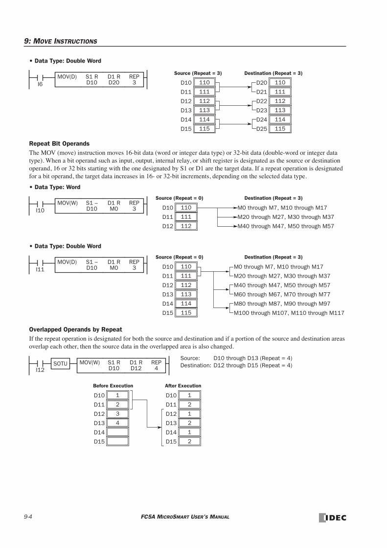
9: MOVE INSTRUCTIONS
• Data Type: Double Word
Repeat Bit OperandsThe MOV (move) instruction moves 16-bit data (word or integer data type) or 32-bit data (double-word or integer data type). When a bit operand such as input, output, internal relay, or shift register is designated as the source or destination operand, 16 or 32 bits starting with the one designated by S1 or D1 are the target data. If a repeat operation is designated for a bit operand, the target data increases in 16- or 32-bit increments, depending on the selected data type.
• Data Type: Word
• Data Type: Double Word
Overlapped Operands by RepeatIf the repeat operation is designated for both the source and destination and if a portion of the source and destination areas overlap each other, then the source data in the overlapped area is also changed.
111D11
110D10
112D12
111D21
110D20
112D22
Source (Repeat = 3) Destination (Repeat = 3)
I6REP3
S1 RD10
D1 RD20
MOV(D)
113D13 113D23
114D14
115D15
114D24
115D25
111D11
110D10
112D12
M20 through M27, M30 through M37
M0 through M7, M10 through M17
M40 through M47, M50 through M57
Source (Repeat = 0) Destination (Repeat = 3)
I10REP3
S1 –D10
D1 RM0
MOV(W)
111D11
110D10
112D12
M20 through M27, M30 through M37
M0 through M7, M10 through M17
M40 through M47, M50 through M57
Source (Repeat = 0) Destination (Repeat = 3)
I11REP3
S1 –D10
D1 RM0
MOV(D)
114D14
113D13
115D15
M80 through M87, M90 through M97
M60 through M67, M70 through M77
M100 through M107, M110 through M117
2D11
1D10
3D12
4D13
D14
D15
2D11
1D10
1D12
2D13
1D14
2D15
Before Execution After Execution
Source: D10 through D13 (Repeat = 4) Destination: D12 through D15 (Repeat = 4)
I12REP4
S1 RD10
D1 RD12
MOV(W)SOTU
9-4 FC5A MICROSMART USER’S MANUAL

9: MOVE INSTRUCTIONS
MOVN (Move Not)
Applicable CPU Modules
Valid Operands
For the valid operand number range, see pages 6-1 and 6-2.
Internal relays M0 through M2557 can be designated as D1. Special internal relays cannot be designated as D1.
When T (timer) or C (counter) is used as S1, the timer/counter current value is read out. When T (timer) or C (counter) is used as D1, the data is written in as a preset value which can be 0 through 65535.
Valid Data Types
Examples: MOVN
FC5A-C10R2/C FC5A-C16R2/C FC5A-C24R2/C FC5A-D16RK1/RS1 FC5A-D32K3/S3
X X X X X
Operand Function I Q M R T C D Constant Repeat
S1 (Source 1) First operand number to move X X X X X X X X 1-99
D1 (Destination 1) First operand number to move to — X X X X X — 1-99
W (word) X
I (integer) X
D (double word) X
L (long) X
F (float) —
S1 NOT → D1 When input is on, 16- or 32-bit data from operand designated by S1 is inverted bit by bit and moved to operand designated by D1.
REP**
S1(R)*****
D1(R)*****
MOVN(*)
When a bit operand such as I (input), Q (output), M (internal relay), or R (shift register) is desig-nated as the source or destination, 16 points (word or integer data type) or 32 points (double-word or long data type) are used. When repeat is designated for a bit operand, the quantity of operand bits increases in 16- or 32-point increments.
When a word operand such as T (timer), C (counter), or D (data register) is designated as the source or destination, 1 point (word or integer data type) or 2 points (double-word or long data type) are used. When repeat is designated for a word operand, the quantity of operand words increases in 1- or 2-point increments.
M10 NOT → M50 When input I0 is on, the 16 internal relays starting with M10 designated by source operand S1 are inverted bit by bit and moved to 16 internal relays starting with M50 designated by destination operand D1.
M10 through M17, M20 through M27 NOT M50 through M57, M60 through M67
The ON/OFF statuses of the 16 internal relays M10 through M17 and M20 through M27 are inverted and moved to 16 internal relays M50 through M57 and M60 through M67. M50 is the LSB (least signif-icant bit), and M67 is the MSB (most significant bit).
Before inversion 0 1 0010 0 0 0 1 0010 1 1
MSB LSBS1
After inversion 1 0 1101 1 1 1 0 1101 0 0
MSB LSBD1
I0REPS1 –
M10D1 –M50
MOVN(W)
(M27-M10):
(M67-M50):
810 NOT → D2 When input I1 is on, decimal constant 810 designated by source operand S1 is converted into 16-bit binary data, and the ON/OFF statuses of the 16 bits are inverted and moved to data register D2 designated by destina-tion operand D1.
D1
D0
64725D2 810
Before inversion (810): 0 0 1000 0 1 0 1 1000 1 0MSB LSBS1
After inversion (64725): 1 1 0111 1 0 1 0 0111 0 1MSB LSBD1
I1REPS1 –
810D1 –D2
MOVN(W)
D30 NOT → D20 When input I2 is on, the data in data register D30 designated by S1 is inverted bit by bit and moved to data register D20 designated by D1.
64605D20
930D30
I2REPS1 –
D30D1 –D20
MOVN(W)
FC5A MICROSMART USER’S MANUAL 9-5

9: MOVE INSTRUCTIONS
IMOV (Indirect Move)
Applicable CPU Modules
Valid Operands
For the valid operand number range, see pages 6-1 and 6-2.
Internal relays M0 through M2557 can be designated as D1. Special internal relays cannot be designated as D1.
When T (timer) or C (counter) is used as S1, S2, or D2, the operand data is the timer/counter current value. When T (timer) or C (counter) is used as D1, the operand data is the timer/counter preset value which can be 0 through 65535.
Either source operand S2 or destination operand D2 does not have to be designated. If S2 or D2 is not designated, the source or destination operand is determined by S1 or D1 without offset.
Make sure that the source data determined by S1 + S2 and the destination data determined by D1 + D2 are within the valid operand range. If the derived source or destination operand is out of the valid operand range, a user program execution error will result, turning on special internal relay M8004 and the ERR LED on the CPU module.
Valid Data Types
Example: IMOV
FC5A-C10R2/C FC5A-C16R2/C FC5A-C24R2/C FC5A-D16RK1/RS1 FC5A-D32K3/S3
X X X X X
Operand Function I Q M R T C D Constant Repeat
S1 (Source 1) Base address to move from X X X X X X X — 1-99
S2 (Source 2) Offset for S1 X X X X X X X — —
D1 (Destination 1) Base address to move to — X X X X X — 1-99
D2 (Destination 2) Offset for D1 X X X X X X X — —
W (word) X
I (integer) —
D (double word) X
L (long) —
F (float) —
S1 + S2 → D1 + D2 When input is on, the values contained in operands desig-nated by S1 and S2 are added to determine the source of data. The 16- or 32-bit data so determined is moved to destination, which is determined by the sum of values contained in operands designated by D1 and D2.
REP**
S1(R)*****
D1(R)*****
IMOV(*) S2*****
D2*****
When a bit operand such as I (input), Q (output), M (internal relay), or R (shift register) is desig-nated as the source or destination, 16 points (word data type) or 32 points (double-word data type) are used. When repeat is designated for a bit operand, the quantity of operand bits increases in 16- or 32-point increments.
When a word operand such as T (timer), C (counter), or D (data register) is designated as the source or destination, 1 point (word data type) or 2 points (double-word data type) are used. When repeat is designated for a word operand, the quantity of operand words increases in 1- or 2-point increments.
D20 + C10 → D10 + D25
Source operand S1 and destination operand D1 determine the type of operand. Source operand S2 and destination operand D2 are the offset values to determine the source and destination oper-ands.
If the current value of counter C10 designated by source operand S2 is 4, the source data is deter-mined by adding the offset to data register D20 designated by source operand S1:
D(20 + 4) = D24
If data register D25 contains a value of 20, the destination is determined by adding the offset to data register D10 designated by destination operand D1:
D(10 + 20) = D30
As a result, when input I0 is on, the data in data register D24 is moved to data register D30.
D23
D22
6450D24
6450D30
D21
D20
20D25
4C10
I0REPS1 –
D20D1 –D10
IMOV(W) S2C10
D2D25
9-6 FC5A MICROSMART USER’S MANUAL
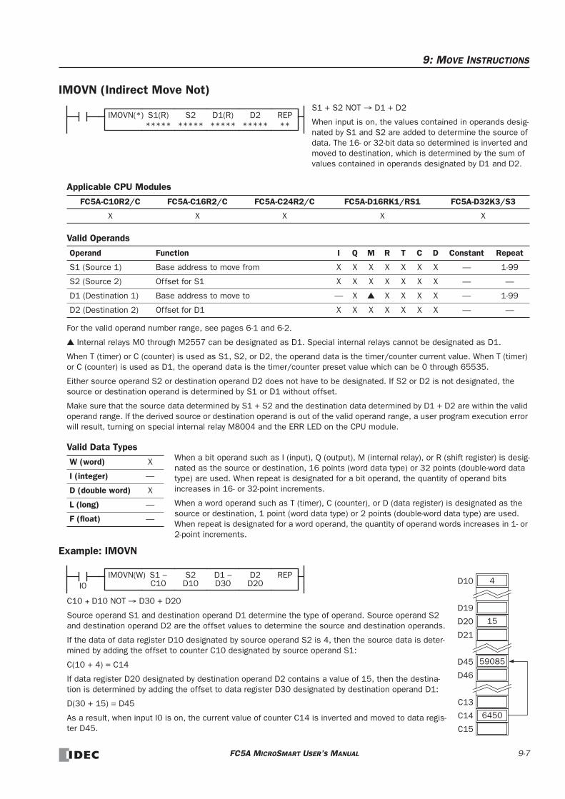
9: MOVE INSTRUCTIONS
IMOVN (Indirect Move Not)
Applicable CPU Modules
Valid Operands
For the valid operand number range, see pages 6-1 and 6-2.
Internal relays M0 through M2557 can be designated as D1. Special internal relays cannot be designated as D1.
When T (timer) or C (counter) is used as S1, S2, or D2, the operand data is the timer/counter current value. When T (timer) or C (counter) is used as D1, the operand data is the timer/counter preset value which can be 0 through 65535.
Either source operand S2 or destination operand D2 does not have to be designated. If S2 or D2 is not designated, the source or destination operand is determined by S1 or D1 without offset.
Make sure that the source data determined by S1 + S2 and the destination data determined by D1 + D2 are within the valid operand range. If the derived source or destination operand is out of the valid operand range, a user program execution error will result, turning on special internal relay M8004 and the ERR LED on the CPU module.
Valid Data Types
Example: IMOVN
FC5A-C10R2/C FC5A-C16R2/C FC5A-C24R2/C FC5A-D16RK1/RS1 FC5A-D32K3/S3
X X X X X
Operand Function I Q M R T C D Constant Repeat
S1 (Source 1) Base address to move from X X X X X X X — 1-99
S2 (Source 2) Offset for S1 X X X X X X X — —
D1 (Destination 1) Base address to move to — X X X X X — 1-99
D2 (Destination 2) Offset for D1 X X X X X X X — —
W (word) X
I (integer) —
D (double word) X
L (long) —
F (float) —
S1 + S2 NOT → D1 + D2
When input is on, the values contained in operands desig-nated by S1 and S2 are added to determine the source of data. The 16- or 32-bit data so determined is inverted and moved to destination, which is determined by the sum of values contained in operands designated by D1 and D2.
REP**
S1(R)*****
D1(R)*****
IMOVN(*) S2*****
D2*****
When a bit operand such as I (input), Q (output), M (internal relay), or R (shift register) is desig-nated as the source or destination, 16 points (word data type) or 32 points (double-word data type) are used. When repeat is designated for a bit operand, the quantity of operand bits increases in 16- or 32-point increments.
When a word operand such as T (timer), C (counter), or D (data register) is designated as the source or destination, 1 point (word data type) or 2 points (double-word data type) are used. When repeat is designated for a word operand, the quantity of operand words increases in 1- or 2-point increments.
C10 + D10 NOT → D30 + D20
Source operand S1 and destination operand D1 determine the type of operand. Source operand S2 and destination operand D2 are the offset values to determine the source and destination operands.
If the data of data register D10 designated by source operand S2 is 4, then the source data is deter-mined by adding the offset to counter C10 designated by source operand S1:
C(10 + 4) = C14
If data register D20 designated by destination operand D2 contains a value of 15, then the destina-tion is determined by adding the offset to data register D30 designated by destination operand D1:
D(30 + 15) = D45
As a result, when input I0 is on, the current value of counter C14 is inverted and moved to data regis-ter D45.
15D20
D19
D21
59085D45
4D10
C15
C13
D46
6450C14
I0REPS1 –
C10D1 –D30
IMOVN(W) S2D10
D2D20
FC5A MICROSMART USER’S MANUAL 9-7

9: MOVE INSTRUCTIONS
BMOV (Block Move)
Applicable CPU Modules
Valid Operands
For the valid operand number range, see pages 6-1 and 6-2.
Internal relays M0 through M2557 can be designated as D1. Special internal relays cannot be designated as D1.
When T (timer) or C (counter) is used as S1 or N-W, the timer/counter current value is read out. When T (timer) or C (counter) is used as D1, the data is written in as a preset value which can be 0 through 65535.
Make sure that the last source data determined by S1+N–1 and the last destination data determined by D1+N–1 are within the valid operand range. If the derived source or destination operand is out of the valid operand range, a user program exe-cution error will result, turning on special internal relay M8004 and the ERR LED on the CPU module.
Valid Data Types
Special Internal Relay M8024: BMOV/WSFT Executing FlagWhile the BMOV or WSFT is executed, M8024 turns on. When completed, M8024 turns off. If the CPU is powered down while executing BMOV or WSFT, M8024 remains on when the CPU is powered up again.
Example: BMOV
FC5A-C10R2/C FC5A-C16R2/C FC5A-C24R2/C FC5A-D16RK1/RS1 FC5A-D32K3/S3
X X X X X
Operand Function I Q M R T C D Constant Repeat
S1 (Source 1) First operand number to move X X X X X X X — —
N-W (N words) Quantity of blocks to move X X X X X X X X —
D1 (Destination 1) First operand number to move to — X X X X X — —
W (word) X
I (integer) —
D (double word) —
L (long) —
F (float) —
S1, S1+1, S1+2, ... , S1+N–1 → D1, D1+1, D1+2, ... , D1+N–1
When input is on, N blocks of 16-bit word data starting with operand designated by S1 are moved to N blocks of destinations, starting with operand designated by D1. N-W specifies the quantity of blocks to move.
BMOV(W) S1*****
D1*****
N-W*****
First 16-bit dataS1
Second 16-bit dataS1+1
Third 16-bit dataS1+2
Nth 16-bit dataS1+N–1
N blocks of 16-bit data
First 16-bit dataD1
Second 16-bit dataD1+1
Third 16-bit dataD1+2
Nth 16-bit dataD1+N–1
N blocks of 16-bit data
Block Move
When a bit operand such as I (input), Q (output), M (internal relay), or R (shift register) is desig-nated as the source, N-W, or destination, 16 points (word data type) are used.
When a word operand such as T (timer), C (counter), or D (data register) is designated as the source, N-W, or destination, 1 point (word data type) is used.
D1D20
D10 through D14 → D20 through D24
When input I0 is turned on, data of 5 data registers starting with D10 desig-nated by source operand S1 is moved to 5 data registers starting with D20 designated by destination operand D1.
12D11
2005D10
25D12
S1D10
N-W5I0
BMOV(W)
12D13
30D14
12D21
2005D20
25D22
12D23
30D24
SOTU
9-8 FC5A MICROSMART USER’S MANUAL

9: MOVE INSTRUCTIONS
IBMV (Indirect Bit Move)
Applicable CPU Modules
Valid Operands
For the valid operand number range, see pages 6-1 and 6-2.
Internal relays M0 through M2557 can be designated as D1. Special internal relays cannot be designated as D1.
When T (timer) or C (counter) is used as S2 or D2, the timer/counter current value is read out.
Make sure that the last source data determined by S1+S2 and the last destination data determined by D1+D2 are within the valid operand range. If the derived source or destination operand is out of the valid operand range, a user program exe-cution error will result, turning on special internal relay M8004 and ERR LED on the CPU module.
Either source operand S2 or destination operand D2 does not have to be designated. If S2 or D2 is not designated, the source or destination operand is determined by S1 or D1 without offset.
Examples: IBMV
Source operand S1 and destination operand D1 determine the type of operand. Source operand S2 and destination operand D2 are the offset values to determine the source and destination operands.
As a result, when input I0 is on, the ON/OFF status of internal relay M15 is moved to output Q44.
FC5A-C10R2/C FC5A-C16R2/C FC5A-C24R2/C FC5A-D16RK1/RS1 FC5A-D32K3/S3
X X X X X
Operand Function I Q M R T C D Constant Repeat
S1 (Source 1) Base address to move from X X X X — — X 0 or 1 1-99
S2 (Source 2) Offset for S1 X X X X X X X 0-65535 —
D1 (Destination 1) Base address to move to — X X — — X — 1-99
D2 (Destination 2) Offset for D1 X X X X X X X 0-65535 —
S1 + S2 → D1 + D2
When input is on, the values contained in operands des-ignated by S1 and S2 are added to determine the source of data. The 1-bit data so determined is moved to desti-nation, which is determined by the sum of values con-tained in operands designated by D1 and D2.
IBMV S1(R)*****
S2*****
D1(R)*****
D2*****
REP**
S1 –M10I0
IBMV S2D10
D1 –Q30
SOTU REPD2C5
M10 + D10 → Q30 + C5
M27 M10M17M20 M15
5th from M10
Q47 Q30Q37Q40
12th from Q30
Q44
If the value of data register D10 designated by source operand S2 is 5, the source data is determined by adding the offset to internal relay M10 designated by source operand S1.
If the current value of counter C5 designated by destination oper-and D2 is 12, the destination is determined by adding the offset to output Q30 designated by destination operand D1.
FC5A MICROSMART USER’S MANUAL 9-9

9: MOVE INSTRUCTIONS
Repeat Operation in the Indirect Bit Move Instructions
Repeat Bit Operands (Source and Destination)If a repeat operation is designated for bit operands such as input, output, internal relay, or shift register, bit operands as many as the repeat cycles are moved.
Repeat Word Operands (Source and Destination)If a repeat operation is designated for word operands such as data register, bit statuses as many as the repeat cycles in the designated data register are moved.
S1 –D10I0
IBMV S25
D1 –D20
SOTU REPD212
D10 + 5 → D20 + 12
Bit 15
Bit 5
Bit 12
Since source operand S1 is a data register and the value of source operand S2 is 5, the source data is bit 5 of data register D10 designated by source operand S1.
Since destination operand D1 is a data register and the value of source operand D2 is 12, the destination is bit 12 of data regis-ter D20 designated by destination operand D1.
As a result, when input I0 is on, the ON/OFF status of data regis-ter D10 bit 5 is moved to data register D20 bit 12.
14 13 12 11 10 9 8 7 6 5 4 3 2 1 0
D10
Bit 15 14 13 12 11 10 9 8 7 6 5 4 3 2 1 0
D20
S1 RM10I1
IBMV S25
D1 RQ30
SOTU REP3
D29
M10 + 5 → Q30 + 9 Repeat = 3
M27 M10M17M20 M15
5th from M10
Q47 Q30Q37Q41
9th from Q30
Q44
Since source operand S1 is internal relay M10 and the value of source operand S2 is 5, the source data is 3 internal relays start-ing with M15.
Since destination operand D1 is output Q30 and the value of desti-nation operand D2 is 9, the destination is 3 outputs starting with Q41.
As a result, when input I1 is on, the ON/OFF statuses of internal relays M15 through M17 are moved to outputs Q41 through Q43.
Q43
S1 RD10I2
IBMV S25
D1 RD20
SOTU REP3
D212
D10 + 5 → D20 + 12 Repeat = 3
Since source operand S1 is data register D10 and the value of source operand S2 is 5, the source data is 3 bits starting with bit 5 of data register D10.
Since destination operand D1 is data register D20 and the value of destination operand D2 is 12, the destination is 3 bits starting with bit 12 of data register D20.
As a result, when input I2 is on, the ON/OFF statuses of data reg-ister D10 bits 5 through 7 are moved to data register D20 bits 12 through 14.
Bit 15
Bit 5
Bit 12
14 13 12 11 10 9 8 7 6 5 4 3 2 1 0
D10
Bit 15 14 13 12 11 10 9 8 7 6 5 4 3 2 1 0
D20
9-10 FC5A MICROSMART USER’S MANUAL

9: MOVE INSTRUCTIONS
IBMVN (Indirect Bit Move Not)
Applicable CPU Modules
Valid Operands
For the valid operand number range, see pages 6-1 and 6-2.
Internal relays M0 through M2557 can be designated as D1. Special internal relays cannot be designated as D1.
When T (timer) or C (counter) is used as S2 or D2, the timer/counter current value is read out.
Make sure that the last source data determined by S1+S2 and the last destination data determined by D1+D2 are within the valid operand range. If the derived source or destination operand is out of the valid operand range, a user program exe-cution error will result, turning on special internal relay M8004 and ERR LED on the CPU module.
Either source operand S2 or destination operand D2 does not have to be designated. If S2 or D2 is not designated, the source or destination operand is determined by S1 or D1 without offset.
Examples: IBMVN
Source operand S1 and destination operand D1 determine the type of operand. Source operand S2 and destination operand D2 are the offset values to determine the source and destination operands.
As a result, when input I0 is on, the ON/OFF status of internal relay M30 is inverted and moved to output Q22.
FC5A-C10R2/C FC5A-C16R2/C FC5A-C24R2/C FC5A-D16RK1/RS1 FC5A-D32K3/S3
X X X X X
Operand Function I Q M R T C D Constant Repeat
S1 (Source 1) Base address to move from X X X X — — X 0 or 1 1-99
S2 (Source 2) Offset for S1 X X X X X X X 0-65535 —
D1 (Destination 1) Base address to move to — X X — — X — 1-99
D2 (Destination 2) Offset for D1 X X X X X X X 0-65535 —
S1 + S2 NOT → D1 + D2
When input is on, the values contained in operands des-ignated by S1 and S2 are added to determine the source of data. The 1-bit data so determined is inverted and moved to destination, which is determined by the sum of values contained in operands designated by D1 and D2.
IBMVN S1(R)*****
S2*****
D1(R)*****
REP**
D2*****
S1 –M20I0
IBMVN S2D10
SOTU D1 –Q10
REPD2C5
M20 + D10 NOT → Q10 + C5
M37 M20M27M30
8th from M20
Q27 Q10Q17Q20
10th from Q10
Q22
If the value of data register D10 designated by source operand S2 is 8, the source data is determined by adding the offset to internal relay M20 designated by source operand S1.
If the current value of counter C5 designated by destination oper-and D2 is 10, the destination is determined by adding the offset to output Q10 designated by destination operand D1.
NOT
FC5A MICROSMART USER’S MANUAL 9-11

9: MOVE INSTRUCTIONS
9-12 FC5A MICROSMART USER’S MANUAL

10: DATA COMPARISON INSTRUCTIONS
IntroductionData can be compared using data comparison instructions, such as equal to, unequal to, less than, greater than, less than or equal to, and greater than or equal to. When the comparison result is true, an output or internal relay is turned on. The repeat operation can also be used to compare more than one set of data.
Three values can also be compared using the ICMP>= instruction.
Since the data comparison instructions are executed in each scan while input is on, a pulse input from a SOTU or SOTD instruction should be used as required.
CMP= (Compare Equal To)
CMP<> (Compare Unequal To)
CMP< (Compare Less Than)
CMP> (Compare Greater Than)
CMP<= (Compare Less Than or Equal To)
CMP>= (Compare Greater Than or Equal To)
Data type W or I: S1 = S2 → D1 on Data type D, L, or F: S1·S1+1 = S2·S2+1 → D1 on When input is on, 16- or 32-bit data designated by source oper-ands S1 and S2 are compared. When S1 data is equal to S2 data, destination operand D1 is turned on. When the condition is not met, D1 is turned off.
REP**
S1(R)*****
D1(R)*****
CMP=(*) S2(R)*****
Data type W or I: S1 ≠ S2 → D1 on Data type D, L, or F: S1·S1+1 ≠ S2·S2+1 → D1 on When input is on, 16- or 32-bit data designated by source oper-ands S1 and S2 are compared. When S1 data is not equal to S2 data, destination operand D1 is turned on. When the condition is not met, D1 is turned off.
REP**
S1(R)*****
D1(R)*****
CMP<>(*) S2(R)*****
Data type W or I: S1 < S2 → D1 on Data type D, L, or F: S1·S1+1 < S2·S2+1 → D1 on When input is on, 16- or 32-bit data designated by source oper-ands S1 and S2 are compared. When S1 data is less than S2 data, destination operand D1 is turned on. When the condition is not met, D1 is turned off.
REP**
S1(R)*****
D1(R)*****
CMP<(*) S2(R)*****
Data type W or I: S1 > S2 → D1 on Data type D, L, or F: S1·S1+1 > S2·S2+1 → D1 on When input is on, 16- or 32-bit data designated by source oper-ands S1 and S2 are compared. When S1 data is greater than S2 data, destination operand D1 is turned on. When the condition is not met, D1 is turned off.
REP**
S1(R)*****
D1(R)*****
CMP>(*) S2(R)*****
Data type W or I: S1 ≤ S2 → D1 on Data type D, L, or F: S1·S1+1 ≤ S2·S2+1 → D1 on When input is on, 16- or 32-bit data designated by source oper-ands S1 and S2 are compared. When S1 data is less than or equal to S2 data, destination operand D1 is turned on. When the condition is not met, D1 is turned off.
REP**
S1(R)*****
D1(R)*****
CMP<=(*) S2(R)*****
Data type W or I: S1 ≥ S2 → D1 on Data type D, L, or F: S1·S1+1 ≥ S2·S2+1 → D1 on When input is on, 16- or 32-bit data designated by source oper-ands S1 and S2 are compared. When S1 data is greater than or equal to S2 data, destination operand D1 is turned on. When the condition is not met, D1 is turned off.
REP**
S1(R)*****
D1(R)*****
CMP>=(*) S2(R)*****
FC5A MICROSMART USER’S MANUAL 10-1
10: DATA COMPARISON INSTRUCTIONS
Applicable CPU Modules
Valid Operands
For the valid operand number range, see pages 6-1 and 6-2.
Internal relays M0 through M2557 can be designated as D1. Special internal relays cannot be designated as D1.
When T (timer) or C (counter) is used as S1 or S2, the timer/counter current value is read out.
When F (float) data type is selected, only data register and constant can be designated as S1 and S2.
When F (float) data type is selected and S1 or S2 does not comply with the normal floating-point format, a user program exe-cution error will result, turning on special internal relay M8004 and ERR LED on the CPU module.
Valid Data Types
Special Internal Relays M8150, M8151, and M8152 in CMP=Three special internal relays are available to indicate the comparison result of the CMP= instruction. Depending on the result, one of the three special internal relays turns on.
When more than one CMP= or ICMP>= instruction is used, M8150, M8151, or M8152 indicates the result of the instruc-tion that was executed last.
Examples: CMP>= The following examples are described using the CMP≥ instruction. Data comparison operation for all other data compari-son instructions is the same for the CMP≥ instruction.
• Data Type: Word
FC5A-C10R2/C FC5A-C16R2/C FC5A-C24R2/C FC5A-D16RK1/RS1 FC5A-D32K3/S3
X X X X X
Operand Function I Q M R T C D Constant Repeat
S1 (Source 1) Data to compare X X X X X X X X 1-99
S2 (Source 2) Data to compare X X X X X X X X 1-99
D1 (Destination 1) Comparison output — X — — — — — 1-99
W (word) X
I (integer) X
D (double word) X
L (long) X
F (float) X
When a bit operand such as I (input), Q (output), M (internal relay), or R (shift register) is desig-nated as the source, 16 points (word or integer data type) or 32 points (double-word or long data type) are used. When repeat is designated for a bit operand, the quantity of operand bits increases in 16- or 32-point increments.
When a word operand such as T (timer), C (counter), or D (data register) is designated as the source, 1 point (word or integer data type) or 2 points (double-word, long, or float data type) are used. When repeat is designated for a word operand, the quantity of operand words increases in 1- or 2-point increments.
When an output or internal relay is designated as the destination, only 1 point is used regard-less of the selected data type. When repeat is designated for the destination, outputs or inter-nal relays as many as the repeat cycles are used.
When S1 > S2, M8150 (greater than) turns on.When S1 = S2, M8151 (equal to) turns on.When S1 < S2, M8152 (less than) turns on.
S2 Value M8150 M8151 M8152 D1 Status
(1) S1 > S2 ON OFF OFF OFF(2) S1 = S2 OFF ON OFF ON(3) S1 < S2 OFF OFF ON OFF
S2
S1
(2)(1) (3)
Small LargeWhen repeat is designated, the comparison result of the last repeat cycle turns on one of the three special internal relays.
I0REPS1 –
D10D1 –Q0
CMP>=(W) S2 –D20
56D20
50D20
Q0 turned off
Q0 turned on
S2 D1
42D10
127D10
S1
10-2 FC5A MICROSMART USER’S MANUAL

10: DATA COMPARISON INSTRUCTIONS
• Data Type: Integer
• Data Type: Double Word
• Data Type: Long
• Data Type: Float
Repeat Operation in the Data Comparison InstructionsThe following examples are described using the CMP≥ instruction of the word and double word data types. Repeat opera-tion for all other data comparison instructions and other data types is the same as the following examples.
Repeat One Source OperandWhen only S1 (source) is designated to repeat, source operands (as many as the repeat cycles, starting with the operand designated by S1) are compared with the operand designated by S2. The comparison results are ANDed and set to the des-tination operand designated by D1.
• Data Type: Word
• Data Type: Double Word
I1REPS1 –
D30D1 –Q1
CMP>=(I) S2 –D40
–3D40
–3D40
Q1 turned off
Q1 turned on
S2 D1
–4D30
12D30
S1
I2REPS1 –
D50D1 –Q2
CMP>=(D) S2 –D60
S2 D1S1
23456789D50·D51 12345678D60·D61 Q2 turned on
23456789D50·D51 34567890D60·D61 Q2 turned off
I3REPS1 –
D70D1 –Q3
CMP>=(L) S2 –D80
S2 D1S1
12345678D70·D71 –12345678D80·D81 Q3 turned on
–12345678D70·D71 34567890D80·D81 Q3 turned off
I4REPS1 –
D90D1 –Q4
CMP>=(F) S2 –D95
S2 D1S1
12.4D90·D91 12.345D95·D96 Q4 turned on
–1D90·D91 –0.99D95·D96 Q4 turned off
I0REP3
S1 RD10
D1 –M10
CMP>=(W) S2 –15
AND15D11
10D10
20D12
M10
S1 (Repeat = 3) D1 (Repeat = 0)S2 (Repeat = 0)
15
15
15
I0REP3
S1 RD20
D1 –M50
CMP>=(D) S2 –D30
D22·D23
D20·D21
D24·D25
AND
S1 (Repeat = 3) D1 (Repeat = 0)S2 (Repeat = 0)
D30·D31
D30·D31
D30·D31
M50
FC5A MICROSMART USER’S MANUAL 10-3
10: DATA COMPARISON INSTRUCTIONS
Repeat Two Source OperandsWhen S1 (source) and S2 (source) are designated to repeat, source operands (as many as the repeat cycles, starting with the operands designated by S1 and S2) are compared with each other. The comparison results are ANDed and set to the destination operand designated by D1.
• Data Type: Word
• Data Type: Double Word
Repeat Source and Destination OperandsWhen S1, S2 (source), and D1 (destination) are designated to repeat, source operands (as many as the repeat cycles, start-ing with the operands designated by S1 and S2) are compared with each other. The comparison results are set to destina-tion operands (as many as the repeat cycles, starting with the operand designated by D1).
• Data Type: Word
• Data Type: Double Word
Comparison Output StatusThe comparison output is usually maintained while the input to the data comparison instruction is off. If the comparison output is on, the on status is maintained when the input is turned off as demonstrated by this program.
This program turns the output off when the input is off.
AND M10I0
REP3
S1 RD10
D1 –M10
CMP>=(W) S2 RD20
20D21
0D20
100D22
S2 (Repeat = 3) D1 (Repeat = 0)
20D11
10D10
30D12
S1 (Repeat = 3)
D22·D23
D20·D21
D24·D25
AND
S1 (Repeat = 3) D1 (Repeat = 0)S2 (Repeat = 3)
D30·D31
D32·D33
D34·D35
M50I0
REP3
S1 RD20
D1 –M50
CMP>=(D) S2 RD30
I0REP3
S1 RD10
D1 RM10
CMP>=(W) S2 RD20
20D21
0D20
100D22
M11 turned on
M10 turned on
M12 turned off
S2 (Repeat = 3) D1 (Repeat = 3)
20D11
10D10
30D12
S1 (Repeat = 3)
D22·D23
D20·D21
D24·D25
S1 (Repeat = 3) D1 (Repeat = 3)S2 (Repeat = 3)
D30·D31
D32·D33
D34·D35
M51
M50
M52
I0REP3
S1 RD20
D1 RM50
CMP>=(D) S2 RD30
Input I0ON
OFF
Comparison D10 ≥ C1D10 < C1
Comparison ONOFF
I0REPS1 –
D10D1 –Q0
CMP>=(W)
Result
Output Q0
S2 –C1
I0
M0
REPS1 –D10
D1 –M0
S2 –C1
Input I0ON
OFF
Comparison D10 ≥ C1D10 < C1
ONOFF
Result
Output Q0
CMP>=(W)
Q0
10-4 FC5A MICROSMART USER’S MANUAL

10: DATA COMPARISON INSTRUCTIONS
ICMP>= (Interval Compare Greater Than or Equal To)
Applicable CPU Modules
Valid Operands
For the valid operand number range, see pages 6-1 and 6-2.
Internal relays M0 through M2557 can be designated as D1. Special internal relays cannot be designated as D1.
When T (timer) or C (counter) is used as S1, S2, or S3, the timer/counter current value is read out.
When F (float) data type is selected, only data register and constant can be designated as S1, S2, and S3.
When F (float) data type is selected and S1, S2, or S3 does not comply with the normal floating-point format, a user program execution error will result, turning on special internal relay M8004 and ERR LED on the CPU module.
When the data of S1 is smaller than that of S3 (S1 < S3), a user program execution error will result, turning on special inter-nal relay M8004 and ERR LED on the CPU module.
Valid Data Types
Special Internal Relays M8150, M8151, and M8152 in ICMP>=Three special internal relays are available to indicate the comparison result of the ICMP>= instruction. Depending on the result, one of the three special internal relays turns on. S1 must always be greater than or equal to S3 (S1 ≥ S3).
When more than one ICMP>= or CMP= instruction is used, M8150, M8151, or M8152 indicates the result of the instruc-tion that was executed last.
FC5A-C10R2/C FC5A-C16R2/C FC5A-C24R2/C FC5A-D16RK1/RS1 FC5A-D32K3/S3
X X X X X
Operand Function I Q M R T C D Constant Repeat
S1 (Source 1) Data to compare X X X X X X X X —
S2 (Source 2) Data to compare X X X X X X X X —
S3 (Source 3) Data to compare X X X X X X X X —
D1 (Destination 1) Comparison output — X — — — — — —
W (word) X
I (integer) X
D (double word) X
L (long) X
F (float) X
Data type W or I: S1 ≥ S2 ≥ S3 → D1 on Data type D, L, F: S1·S1+1 ≥ S2·S2+1≥ S3·S3+1 → D1 on
When input is on, the 16- or 32-bit data designated by S1, S2, and S3 are compared. When the condition is met, destination operand D1 is turned on. When the condition is not met, D1 is turned off.
ICMP>=(*) S1*****
S2*****
S3*****
D1*****
When a bit operand such as I (input), Q (output), M (internal relay), or R (shift register) is desig-nated as the source, 16 points (word or integer data type) or 32 points (double-word or long data type) are used.
When a word operand such as T (timer), C (counter), or D (data register) is designated as the source, 1 point (word or integer data type) or 2 points (double-word, long, or float data type) are used.
The destination uses only one output or internal relay regardless of the selected data type.
When S2 > S1, M8150 turns on.When S2 < S3, M8151 turns on.When S1 > S2 > S3, M8152 turns on.
S2 Value M8150 M8151 M8152 D1 Status
(1) S2 < S3 OFF ON OFF OFF(2) S2 = S3 OFF OFF OFF ON
(3) S3 < S2 < S1 OFF OFF ON ON(4) S2 = S1 OFF OFF OFF ON(5) S2 > S1 ON OFF OFF OFFS2
S3 S1M8151 M8152 M8150
(2)(1) (3) (5)(4)
Small Large
FC5A MICROSMART USER’S MANUAL 10-5

10: DATA COMPARISON INSTRUCTIONS
Example: ICMP>=
D1Q1
When input I0 is turned on, data of data registers D10, D11, and D12 designated by source operands S1, S2, and S3 are compared. When the condition is met, internal relay Q1 designated by destination operand D1 is turned on. When the condi-tion is not met, Q1 is turned off.
S1D10I0
ICMP>=(W) S2D11
S3D12
SOTUD10 ≥ D11 ≥ D12 → Q1 goes on
15D11
S2
17D10
S1
15D12
S3
> = Q1 goes on
D1 M8151 M8152 M8004M8150
OFF OFF OFF OFF
18D1115D10 19D12< < Q1 goes off ON ON OFF ON
10-6 FC5A MICROSMART USER’S MANUAL

11: BINARY ARITHMETIC INSTRUCTIONS
IntroductionThe binary arithmetic instructions make it possible for the user to program computations using addition, subtraction, mul-tiplication, and division. For addition and subtraction operands, internal relay M8003 is used to carry or to borrow.
The ROOT instruction can be used to calculate the square root of the value stored in one or two data registers.
ADD (Addition)
SUB (Subtraction)
MUL (Multiplication)
DIV (Division)
Data type W or I: S1 + S2 → D1, CY Data type D, L, or F: S1·S1+1 + S2·S2+1 → D1·D1+1, CY
When input is on, 16- or 32-bit data designated by source oper-ands S1 and S2 are added. The result is set to destination oper-and D1 and carry (M8003).
REP**
S1(R)*****
D1(R)*****
ADD(*) S2(R)*****
Data type W or I: S1 – S2 → D1, BW Data type D, L, or F: S1·S1+1 – S2·S2+1 → D1·D1+1, BW
When input is on, 16- or 32-bit data designated by source oper-and S2 is subtracted from 16- or 32-bit data designated by source operand S1. The result is set to destination operand D1 and borrow (M8003).
REP**
S1(R)*****
D1(R)*****
SUB(*) S2(R)*****
Data type W or I: S1 × S2 → D1·D1+1 Data type D, L, or F: S1·S1+1 × S2·S2+1 → D1·D1+1
When input is on, 16- or 32-bit data designated by source oper-and S1 is multiplied by 16- or 32-bit data designated by source operand S2. The result is set to destination operand D1.
When the result exceeds the valid range for data types D or L, the ERR LED and special internal relay M8004 (user program execution error) are turned on.
REP**
S1(R)*****
D1(R)*****
MUL(*) S2(R)*****
Data type W or I: S1 ÷ S2 → D1 (quotient), D1+1 (remainder)
Data type D or L: S1·S1+1 ÷ S2·S2+1 → D1·D1+1 (quotient),
D1+2·D1+3 (remainder)
Data type F: S1·S1+1 ÷ S2·S2+1 → D1·D1+1 (quotient)
When input is on, 16- or 32-bit data designated by source oper-and S1 is divided by 16- or 32-bit data designated by source operand S2. The quotient is set to 16- or 32-bit destination oper-and D1, and the remainder is set to the next 16- or 32-bit data. Data type F does not generate a remainder.
When S2 is 0 (dividing by 0), the ERR LED and special internal relay M8004 (user program execution error) are turned on.
A user program execution error also occurs in the following divi-sion operations.
Data type I: –32768 ÷ (–1) Data type L: –2147483648 ÷ (–1)
REP**
S1(R)*****
D1(R)*****
DIV(*) S2(R)*****
FC5A MICROSMART USER’S MANUAL 11-1

11: BINARY ARITHMETIC INSTRUCTIONS
Applicable CPU Modules
Valid Operands
For the valid operand number range, see pages 6-1 and 6-2.
Internal relays M0 through M2557 can be designated as D1. Special internal relays cannot be designated as D1.
When T (timer) or C (counter) is used as S1 or S2, the timer/counter current value is read out. When T (timer) or C (counter) is used as D1, the data is written in as a preset value which can be 0 through 65535.
When F (float) data type is selected, only data register and constant can be designated as S1 and S2.
When F (float) data type is selected and S1 or S2 does not comply with the normal floating-point format, a user program exe-cution error will result, turning on special internal relay M8004 and ERR LED on the CPU module.
Since the binary arithmetic instructions are executed in each scan while input is on, a pulse input from a SOTU or SOTD instruction should be used as required.
Valid Data Types
Using Carry or Borrow SignalsWhen the D1 (destination) data is out of the valid data range as a result of any binary arithmetic operation, a carry or bor-row occurs, and special internal relay M8003 is turned on.
FC5A-C10R2/C FC5A-C16R2/C FC5A-C24R2/C FC5A-D16RK1/RS1 FC5A-D32K3/S3
X X X X X
Operand Function I Q M R T C D Constant Repeat
S1 (Source 1) Data for calculation X X X X X X X X 1-99
S2 (Source 2) Data for calculation X X X X X X X X 1-99
D1 (Destination 1) Destination to store results — X X X X X — 1-99
W (word) X
I (integer) X
D (double word) X
L (long) X
F (float) X
Data Type Carry/borrow occurs when D1 is out of the range between
W (word) 0 and 65,535
I (integer) –32,768 and 32,767
D (double word) 0 and 4,294,967,295
L (long) –2,147,483,648 and 2,147,483,647
F (float)–3.402823×1038 and –1.175495×10–38
1.175495×10–38 and 3.402823×1038
When a bit operand such as I (input), Q (output), M (internal relay), or R (shift register) is desig-nated as the source, 16 points (word or integer data type) or 32 points (double-word or long data type) are used. When repeat is designated for a bit operand, the quantity of operand bits increases in 16- or 32-point increments.
When a word operand such as T (timer), C (counter), or D (data register) is designated as the source, 1 point (word or integer data type) or 2 points (double-word or long data type) are used. When repeat is designated for a word operand, the quantity of operand words increases in 1- or 2-point increments.
11-2 FC5A MICROSMART USER’S MANUAL

11: BINARY ARITHMETIC INSTRUCTIONS
Examples: ADD
• Data Type: WordThis example demonstrates the use of a carry signal from special internal relay M8003 to set an alarm signal.
• Data Type: Integer
• Data Type: Double Word
• Data Type: Long
• Data Type: Float
Example: SUB
• Data Type: WordThe following example demonstrates the use of special internal relay M8003 to process a borrow.
I0REPS2 –
500D1 –D2
SOTU
M8003
I1
D2 + 500 → D2
When a carry occurs, output Q0 is set as a warning indica-tor.
When the acknowledge pushbutton (input I1) is pressed, the warning indicator is reset.
AcknowledgePushbutton
S1 –D2
ADD(W)
Q0S
Q0R
I0REPS2 –
D20D1 –D30
S1 –D10
ADD(I) –4D10 + –15D30–11D20
I0REPS2 –
D20D1 –D30
S1 –D10
ADD(D)
+1957400D10·D11 4112600D20·D21 6070000D30·D31
I0REPS2 –
D20D1 –D30
S1 –D10
ADD(L)
+216283D10·D11 –964355D20·D21 –748072D30·D31
I0REPS2 –
D20D1 –D30
S1 –D10
ADD(F)
+1.414D10·D11 3.14D20·D21 4.554D30·D31
I0SOTU
M8003
D12 – 7000 → D12
To process borrowing so that the number of times a borrow occurs is subtracted from D13.
When a borrow occurs, D13 is decremented by one.
REPS2 –7000
D1 –D12
S1 –D12
SUB(W)
REPS2 –1
D1 –D13
S1 –D13
SUB(W)
FC5A MICROSMART USER’S MANUAL 11-3

11: BINARY ARITHMETIC INSTRUCTIONS
Examples: MUL
• Data Type: Word
• Data Type: Integer
• Data Type: Double Word
Note: In multiplication of double word data type, the lower 32-bit data of the result is set to destination operand D1·D1+1.
• Data Type: Long
Note: In multiplication of long data type, the lower 32-bit data of the result is set to destination operand D1·D1+1.
• Data Type: Float
Note: Since the destination uses two word operands in the multiplication operation, data register D1999 cannot be used as destination operand D1. When using a bit operand such as internal relay for destination, 32 internal relays are required; so internal relay M2521 or a larger number cannot be used as destination operand D1.
I1REPS2 –
D20D1 –D30
S1 –D10
MUL(W)D10 × 300000
(000493E0h)500
(01F4h)600
(0258h)D20 D30·D31
When input I1 is on, data of D10 is multiplied by data of D20, and the result is set to D30 and D31.
D31 37856(93E0h)
D30 4(0004h)
I1REPS2 –
D20D1 –D30
S1 –D10
MUL(I)D10 × –300000
(FFFB6C20h)–500
(FE0Ch)600
(0258h)D20 D30·D31
D31 27680(6C20h)
D30 65531(FFFBh)
I1REPS2 –
D20D1 –D30
S1 –D10
MUL(D)
×100000D10·D11 5000D20·D21 500000000D30·D31
I1REPS2 –
D20D1 –D30
S1 –D10
MUL(L)
×–100000D10·D11 –5000D20·D21 500000000D30·D31
I1REPS2 –
D20D1 –D30
S1 –D10
MUL(F)
×4.554D10·D11 1.414D20·D21 6.439356D30·D31
11-4 FC5A MICROSMART USER’S MANUAL

11: BINARY ARITHMETIC INSTRUCTIONS
Examples: DIV
• Data Type: Word
Note: Since the destination uses two word operands in the division operation of word data type, data register D1999 cannot be used as destination operand D1. When using a bit operand such as internal relay for destination, 32 internal relays are required; so M2521 or a larger number cannot be used as destination operand D1.
• Data Type: Integer
Note: Since the destination uses two word operands in the division operation of integer data type, data register D1999 can-not be used as destination operand D1. When using a bit operand such as internal relay for destination, 32 internal relays are required; so M2521 or a larger number cannot be used as destination operand D1.
• Data Type: Double Word
Note: Since the destination uses four word operands in the division operation of double-word data type, data registers D1997 through D1999 cannot be used as destination operand D1. When using a bit operand such as internal relay for des-tination, 64 internal relays are required; so M2481 or a larger number cannot be used as destination operand D1.
• Data Type: Long
Note: Since the destination uses four word operands in the division operation of long data type, data registers D1997 through D1999 cannot be used as destination operand D1. When using a bit operand such as internal relay for destination, 64 internal relays are required; so M2481 or a larger number cannot be used as destination operand D1.
• Data Type: Float
Note: Since the destination uses two word operands in the division operation of float data type, data register D1999 cannot be used as destination operand D1.
When input I2 is on, data of D10 is divided by data of D20. The quo-tient is set to D30, and the remainder is set to D31.
I2REPS2 –
D20D1 –D30
S1 –D10
DIV(W)Quotient Remainder
50D10 ÷ 7D307D20 1D31
I2REPS2 –
D20D1 –D30
S1 –D10
DIV(I)Quotient Remainder
50D10 ÷ –7D30–7D20 1D31
I1REPS2 –
D20D1 –D30
S1 –D10
DIV(D)
÷100000D10·D11 70000D20·D21 1D30·D31 30000D32·D33
Quotient Remainder
I1REPS2 –
D20D1 –D30
S1 –D10
DIV(L)
÷100000D10·D11 –70000D20·D21 –1D30·D31 30000D32·D33
Quotient Remainder
I1REPS2 –
D20D1 –D30
S1 –D10
DIV(F)
÷4.43996D10·D11 3.14D20·D21 1.414D30·D31
Quotient
FC5A MICROSMART USER’S MANUAL 11-5

11: BINARY ARITHMETIC INSTRUCTIONS
Repeat Operation in the ADD and SUB InstructionsSource operands S1 and S2 and destination operand D1 can be designated to repeat individually or in combination. When destination operand D1 is not designated to repeat, the final result is set to destination operand D1. When repeat is desig-nated, consecutive operands as many as the repeat cycles starting with the designated operand are used. Since the repeat operation works similarly on the ADD (addition) and SUB (subtraction) instructions, the following examples are described using the ADD instruction.
Repeat One Source Operand
• Data Type: Word and IntegerWhen only S1 (source) is designated to repeat, the final result is set to destination operand D1.
• Data Type: Double Word, Long, and FloatWhen only S1 (source) is designated to repeat, the final result is set to destination operand D1·D1+1.
Repeat Destination Operand Only
• Data Type: Word and IntegerWhen only D1 (destination) is designated to repeat, the same result is set to 3 operands starting with D1.
• Data Type: Double Word, Long, and FloatWhen only D1 (destination) is designated to repeat, the same result is set to 3 operands starting with D1·D1+1.
Repeat Two Source Operands
• Data Type: Word and IntegerWhen S1 and S2 (source) are designated to repeat, the final result is set to destination operand D1.
• Data Type: Double Word, Long, and FloatWhen S1 and S2 (source) are designated to repeat, the final result is set to destination operand D1·D1+1.
I1REP3
S1 RD10
D1 –D30
15D11
10D10
20D12
S1 (Repeat = 3) D1 (Repeat = 0)S2 –D20
S2 (Repeat = 0)
+
+
+
(40)D30
(35)D30
45D30
25D20
25D20
25D20
SOTU ADD(W)
I1REP3
S1 RD10
D1 –D30
D12·D13
D10·D11
D14·D15
S1 (Repeat = 3) D1 (Repeat = 0)S2 –D20
S2 (Repeat = 0)
+
+
+
(D30·D31)
(D30·D31)
D30·D31
D20·D21
D20·D21
D20·D21
SOTU ADD(D)
I1REP3
S1 –D10
D1 RD30
10D10
10D10
10D10
S1 (Repeat = 0) D1 (Repeat = 3)S2 –D20
S2 (Repeat = 0)
+
+
+
35D31
35D30
35D32
25D20
25D20
25D20
SOTU ADD(W)
I1REP3
S1 –D10
D1 RD30
D10·D11
D10·D11
D10·D11
S1 (Repeat = 0) D1 (Repeat = 3)S2 –D20
S2 (Repeat = 0)
+
+
+
D32·D33
D30·D31
D34·D35
D20·D21
D20·D21
D20·D21
SOTU ADD(D)
I1REP3
S1 RD10
D1 –D30
15D11
10D10
20D12
S1 (Repeat = 3) D1 (Repeat = 0)S2 RD20
S2 (Repeat = 3)
+
+
+
(50)D30
(35)D30
65D30
35D21
25D20
45D22
SOTU ADD(W)
I1REP3
S1 RD10
D1 –D30
D12·D13
D10·D11
D14·D15
S1 (Repeat = 3) D1 (Repeat = 0)S2 RD20
S2 (Repeat = 3)
+
+
+
(D30·D31)
(D30·D31)
D30·D31
D22·D23
D20·D21
D24·D25
SOTU ADD(D)
11-6 FC5A MICROSMART USER’S MANUAL
11: BINARY ARITHMETIC INSTRUCTIONS
Repeat Source and Destination Operands
• Data Type: Word and IntegerWhen S1 (source) and D1 (destination) are designated to repeat, different results are set to 3 operands starting with D1.
• Data Type: Double Word, Long, and FloatWhen S1 (source) and D1 (destination) are designated to repeat, different results are set to 3 operands starting with D1·D1+1.
Repeat All Source and Destination Operands
• Data Type: Word and IntegerWhen all operands are designated to repeat, different results are set to 3 operands starting with D1.
• Data Type: Double Word, Long, and FloatWhen all operands are designated to repeat, different results are set to 3 operands starting with D1·D1+1.
Note: Special internal relay M8003 (carry/borrow) is turned on when a carry or borrow occurs in the last repeat operation. When a user program execution error occurs in any repeat operation, special internal relay M8004 (user program execution error) and the ERR LED are turned on and maintained while operation for other instructions is continued.
I1REP3
S1 RD10
D1 RD30
15D11
10D10
20D12
S1 (Repeat = 3) D1 (Repeat = 3)S2 –D20
S2 (Repeat = 0)
+
+
+
40D31
35D30
45D32
25D20
25D20
25D20
SOTU ADD(W)
I1REP3
S1 RD10
D1 RD30
D12·D13
D10·D11
D14·D15
S1 (Repeat = 3) D1 (Repeat = 3)S2 –D20
S2 (Repeat = 0)
+
+
+
D32·D33
D30·D31
D34·D35
D20·D21
D20·D21
D20·D21
SOTU ADD(D)
I1REP3
S1 RD10
D1 RD30
15D11
10D10
20D12
S1 (Repeat = 3) D1 (Repeat = 3)S2 RD20
S2 (Repeat = 3)
+
+
+
50D31
35D30
65D32
35D21
25D20
45D22
SOTU ADD(W)
I1REP3
S1 RD10
D1 RD30
D12·D13
D10·D11
D14·D15
S1 (Repeat = 3) D1 (Repeat = 3)S2 RD20
S2 (Repeat = 3)
+
+
+
D32·D33
D30·D31
D34·D35
D22·D23
D20·D21
D24·D25
SOTU ADD(D)
FC5A MICROSMART USER’S MANUAL 11-7

11: BINARY ARITHMETIC INSTRUCTIONS
Repeat Operation in the MUL InstructionSince the MUL (multiplication) instruction uses two destination operands, the result is stored to destination operands as described below. Source operands S1 and S2 and destination operand D1 can be designated to repeat individually or in combination. When destination operand D1 is not designated to repeat, the final result is set to destination operand D1 and D1+1. When repeat is designated, consecutive operands as many as the repeat cycles starting with the designated operand are used.
Since the repeat operation works similarly on the word and integer data types, the following examples are described using the word data type.
Repeat One Source OperandWhen only S1 (source) is designated to repeat, the final result is set to destination operand D1·D1+1.
• Data Type: Word and Integer
• Data Type: Double Word, Long, and Float
Repeat Destination Operand OnlyWhen only D1 (destination) is designated to repeat, the same result is set to 3 operands starting with D1·D1+1.
• Data Type: Word and Integer
• Data Type: Double Word, Long, and Float
Repeat Two Source OperandsWhen S1 and S2 (source) are designated to repeat, the final result is set to destination operand D1·D1+1.
• Data Type: Word and Integer
• Data Type: Double Word, Long, and Float
I1REP3
S1 RD10
D1 –D30 D10
S1 (Repeat = 3) D1 (Repeat = 0)S2 –D20
S2 (Repeat = 0)
× D20D11D12
××
D20D20
SOTU MUL(W)
(D30·D31)(D30·D31)
D30·D31
I1REP3
S1 RD10
D1 –D30
D12·D13D10·D11
D14·D15
S1 (Repeat = 3) D1 (Repeat = 0)S2 –D20
S2 (Repeat = 0)
×××
(D30·D31)(D30·D31)
D30·D31D20·D21D20·D21
D20·D21
SOTU MUL(D)
I1REP3
S1 –D10
D1 RD30 D10
S1 (Repeat = 0) D1 (Repeat = 3)S2 –D20
S2 (Repeat = 0)
× D20D10D10
××
D20D20
SOTU MUL(W)
D32·D33D30·D31
D34·D35
I1REP3
S1 –D10
D1 RD30
D10·D11D10·D11
D10·D11
S1 (Repeat = 0) D1 (Repeat = 3)S2 –D20
S2 (Repeat = 0)
×××
D32·D33D30·D31
D34·D35D20·D21D20·D21
D20·D21
SOTU MUL(D)
I1REP3
S1 RD10
D1 –D30 D10
S1 (Repeat = 3) D1 (Repeat = 0)S2 RD20
S2 (Repeat = 3)
× D20D11D12
××
D21D22
SOTU MUL(W)
(D30·D31)(D30·D31)
D30·D31
I1REP3
S1 RD10
D1 –D30
D12·D13D10·D11
D14·D15
S1 (Repeat = 3) D1 (Repeat = 0)S2 RD20
S2 (Repeat = 3)
×××
(D30·D31)(D30·D31)
D30·D31D22·D23D20·D21
D24·D25
SOTU MUL(D)
11-8 FC5A MICROSMART USER’S MANUAL
11: BINARY ARITHMETIC INSTRUCTIONS
Repeat Source and Destination OperandsWhen S1 (source) and D1 (destination) are designated to repeat, different results are set to 3 operands starting with D1·D1+1.
• Data Type: Word and Integer
• Data Type: Double Word, Long, and Float
Repeat All Source and Destination OperandsWhen all operands are designated to repeat, different results are set to 3 operands starting with D1·D1+1.
• Data Type: Word and Integer
• Data Type: Double Word, Long, and Float
I1REP3
S1 RD10
D1 RD30 D10
S1 (Repeat = 3) D1 (Repeat = 3)S2 –D20
S2 (Repeat = 0)
× D20D11D12
××
D20D20
SOTU MUL(W)
D32·D33D30·D31
D34·D35
I1REP3
S1 RD10
D1 RD30
D12·D13D10·D11
D14·D15
S1 (Repeat = 3) D1 (Repeat = 3)S2 –D20
S2 (Repeat = 0)
×××
D32·D33D30·D31
D34·D35D20·D21D20·D21
D20·D21
SOTU MUL(D)
I1REP3
S1 RD10
D1 RD30 D10
S1 (Repeat = 3) D1 (Repeat = 3)S2 RD20
S2 (Repeat = 3)
× D20D11D12
××
D21D22
SOTU MUL(W)
D32·D33D30·D31
D34·D35
I1REP3
S1 RD10
D1 RD30
D12·D13D10·D11
D14·D15
S1 (Repeat = 3) D1 (Repeat = 3)S2 RD20
S2 (Repeat = 3)
×××
D32·D33D30·D31
D34·D35D22·D23D20·D21
D24·D25
SOTU MUL(D)
FC5A MICROSMART USER’S MANUAL 11-9

11: BINARY ARITHMETIC INSTRUCTIONS
Repeat Operation in the DIV InstructionSince the DIV (division) instruction (except the float data type) uses two destination operands, the quotient and remainder are stored as described below. Source operands S1 and S2 and destination operand D1 can be designated to repeat individ-ually or in combination. When destination operand D1 is not designated to repeat, the final result is set to destination oper-and D1 (quotient) and D1+1 (remainder). When repeat is designated, consecutive operands as many as the repeat cycles starting with the designated operand are used.
Division instructions in the float data type do not generate remainders and use two consecutive data registers to store quo-tients. When repeat is designated for destination of the float data type, consecutive data registers as many as the repeat cycles are used.
Repeat One Source Operand
• Data Type: Word and IntegerWhen only S1 (source) is designated to repeat, the final result is set to destination operands D1 and D1+1.
• Data Type: Double Word and LongWhen only S1 (source) is designated to repeat, the final result is set to destination operands D1·D1+1 and D1+2·D1+3.
• Data Type: FloatWhen only S1 (source) is designated to repeat, the final result is set to destination operands D1·D1+1.
Repeat Destination Operand Only
• Data Type: Word and IntegerWhen only D1 (destination) is designated to repeat, the same result is set to 6 operands starting with D1.
• Data Type: Double Word and LongWhen only D1 (destination) is designated to repeat, the same result is set to 6 operands starting with D1·D1+1.
• Data Type: FloatWhen only D1 (destination) is designated to repeat, the same result is set to 3 operands starting with D1·D1+1.
I1REP3
S1 RD10
D1 –D30 D10
S1 (Repeat = 3) D1 (Repeat = 0)S2 –D20
S2 (Repeat = 0)
÷ (D30)D20 (D31)D11D12
÷÷
D20D20
(D30)D30
(D31)D31
Quotient Remainder
SOTU DIV(W)
I1REP3
S1 RD10
D1 –D30 D10·D11
S1 (Repeat = 3) D1 (Repeat = 0)S2 –D20
S2 (Repeat = 0)
÷ (D30·D31)D20·D21 (D32·D33)D12·D13D14·D15
÷÷
D20·D21D20·D21
(D30·D31)D30·D31
(D32·D33)D32·D33
Quotient Remainder
SOTU DIV(D)
I1REP3
S1 RD10
D1 –D30
D12·D13D10·D11
D14·D15
S1 (Repeat = 3) D1 (Repeat = 0)S2 –D20
S2 (Repeat = 0)
÷÷÷
(D30·D31)(D30·D31)
D30·D31D20·D21D20·D21
D20·D21
SOTU DIV(F)
Quotient
I1REP3
S1 –D10
D1 RD30 D10
S1 (Repeat = 0) D1 (Repeat = 3)S2 –D20
S2 (Repeat = 0)
÷ D30D20 D33D10D10
÷÷
D20D20
D31D32
D34D35
Quotient Remainder
SOTU DIV(W)
I1REP3
S1 –D10
D1 RD30 D10·D11
S1 (Repeat = 0) D1 (Repeat = 3)S2 –D20
S2 (Repeat = 0)
÷ D30·D31D20·D21 D36·D37D10·D11D10·D11
÷÷
D20·D21D20·D21
D32·D33D34·D35
D38·D39D40·D41
Quotient Remainder
SOTU DIV(D)
I1REP3
S1 –D10
D1 RD30
D10·D11D10·D11
D10·D11
S1 (Repeat = 0) D1 (Repeat = 3)S2 –D20
S2 (Repeat = 0)
÷÷÷
D32·D33D30·D31
D34·D35D20·D21D20·D21
D20·D21
SOTU DIV(F)
Quotient
11-10 FC5A MICROSMART USER’S MANUAL

11: BINARY ARITHMETIC INSTRUCTIONS
Repeat Two Source Operands
• Data Type: Word and IntegerWhen S1 and S2 (source) are designated to repeat, the final result is set to destination operands D1 and D1+1.
• Data Type: Double Word and LongWhen S1 and S2 (source) are designated to repeat, the final result is set to destination operands D1·D1+1 and D1+2·D1+3.
• Data Type: FloatWhen S1 and S2 (source) are designated to repeat, the final result is set to destination operands D1·D1+1.
Repeat Source and Destination Operands
• Data Type: Word and IntegerWhen S1 (source) and D1 (destination) are designated to repeat, different results are set to 6 operands starting with D1.
• Data Type: Double Word and LongWhen S1 (source) and D1 (destination) are designated to repeat, different results are set to 6 operands starting with D1·D1+1.
• Data Type: FloatWhen S1 (source) and D1 (destination) are designated to repeat, different results are set to 3 operands starting with D1·D1+1.
I1REP3
S1 RD10
D1 –D30 D10
S1 (Repeat = 3) D1 (Repeat = 0)S2 RD20
S2 (Repeat = 3)
÷ (D30)D20 (D31)D11D12
÷÷
D21D22
(D30)D30
(D31)D31
Quotient Remainder
SOTU DIV(W)
I1REP3
S1 RD10
D1 –D30 D10·D11
S1 (Repeat = 3) D1 (Repeat = 0)S2 RD20
S2 (Repeat = 3)
÷ (D30·D31)D20·D21 (D32·D33)D12·D13D14·D15
÷÷
D22·D23D24·D25
(D30·D31)D30·D31
(D32·D33)D32·D33
Quotient Remainder
SOTU DIV(D)
I1REP3
S1 RD10
D1 –D30
D12·D13D10·D11
D14·D15
S1 (Repeat = 3) D1 (Repeat = 0)S2 RD20
S2 (Repeat = 3)
÷÷÷
(D30·D31)(D30·D31)
D30·D31D22·D23D20·D21
D24·D25
SOTU DIV(F)
Quotient
I1REP3
S1 RD10
D1 RD30 D10
S1 (Repeat = 3) D1 (Repeat = 3)S2 –D20
S2 (Repeat = 0)
÷ D30D20 D33D11D12
÷÷
D20D20
D31D32
D34D35
Quotient Remainder
SOTU DIV(W)
I1REP3
S1 RD10
D1 RD30 D10·D11
S1 (Repeat = 3) D1 (Repeat = 3)S2 –D20
S2 (Repeat = 0)
÷ D30·D31D20·D21 D36·D37D12·D13D14·D15
÷÷
D20·D21D20·D21
D32·D33D34·D35
D38·D39D40·D41
Quotient Remainder
SOTU DIV(D)
I1REP3
S1 RD10
D1 RD30
D12·D13D10·D11
D14·D15
S1 (Repeat = 0) D1 (Repeat = 3)S2 –D20
S2 (Repeat = 0)
÷÷÷
D32·D33D30·D31
D34·D35D20·D21D20·D21
D20·D21
SOTU DIV(F)
Quotient
FC5A MICROSMART USER’S MANUAL 11-11

11: BINARY ARITHMETIC INSTRUCTIONS
Repeat All Source and Destination Operands
• Data Type: Word and IntegerWhen all operands are designated to repeat, different results are set to 6 operands starting with D1.
• Data Type: Double Word and LongWhen all operands are designated to repeat, different results are set to 6 operands starting with D1·D1+1.
• Data Type: FloatWhen all operands are designated to repeat, different results are set to 3 operands starting with D1·D1+1.
Note: When a user program execution error occurs in any repeat operation, special internal relay M8004 (user program exe-cution error) and the ERR LED are turned on and maintained while operation for other instructions is continued.
I1REP3
S1 RD10
D1 RD30 D10
S1 (Repeat = 3) D1 (Repeat = 3)S2 RD20
S2 (Repeat = 3)
÷ D30D20 D33D11D12
÷÷
D21D22
D31D32
D34D35
Quotient Remainder
SOTU DIV(W)
I1REP3
S1 RD10
D1 RD30 D10·D11
S1 (Repeat = 3) D1 (Repeat = 3)S2 RD20
S2 (Repeat = 3)
÷ D30·D31D20·D21 D36·D37D12·D13D14·D15
÷÷
D22·D23D24·D25
D32·D33D34·D35
D38·D39D40·D41
Quotient Remainder
SOTU DIV(D)
I1REP3
S1 RD10
D1 RD30
D12·D13D10·D11
D14·D15
S1 (Repeat = 0) D1 (Repeat = 3)S2 RD20
S2 (Repeat = 0)
÷÷÷
D32·D33D30·D31
D34·D35D22·D23D20·D21
D24·D25
SOTU DIV(F)
Quotient
11-12 FC5A MICROSMART USER’S MANUAL

11: BINARY ARITHMETIC INSTRUCTIONS
ROOT (Root)
Applicable CPU Modules
Valid Operands
For the valid operand number range, see pages 6-1 and 6-2.
When F (float) data type is selected and source operand S1 contains a negative value, a user program execution error will result, turning on special internal relay M8004 and the ERR LED on the CPU module.
When F (float) data type is selected and S1 does not comply with the normal floating-point format, a user program execution error will result, turning on special internal relay M8004 and ERR LED on the CPU module.
Since the ROOT instruction is executed in each scan while input is on, a pulse input from a SOTU or SOTD instruction should be used as required.
Valid Data Types
Examples: ROOT
FC5A-C10R2/C FC5A-C16R2/C FC5A-C24R2/C FC5A-D16RK1/RS1 FC5A-D32K3/S3
X X X X X
Operand Function I Q M R T C D Constant Repeat
S1 (Source 1) Binary data — — — — — — X X —
D1 (Destination 1) Destination to store results — — — — — — X — —
W (word) X
I (integer) —
D (double word) X
L (long) —
F (float) X
Data type W:
When input is on, the square root of operand designated by S1 is extracted and is stored to the destination designated by D1.
The square root is calculated to two decimals, omitting the figures below the second place of decimals, and multiplied by 100.
Data type D:
When input is on, the square root of operand designated by S1·S1+1 is extracted and is stored to the destination designated by D1·D1+1.
The square root is calculated to two decimals, omitting the figures below the second place of decimals, and multiplied by 100.
Data type F:
When input is on, the square root of operand designated by S1·S1+1 is extracted and is stored to the destination designated by D1·D1+1.
S1 → D1
S1·S1+1 → D1·D1+1
S1·S1+1 → D1·D1+1
ROOT(*) S1*****
D1*****
When a word operand such as D (data register) is designated as the source or destination, 1 point (word data type) or 2 points (double-word or float data type) are used.
D1D20I0
ROOT(W) S1D10 55D10 741D20
Before Execution After Execution
D1D21I1
ROOT(D) S1D11
D1D23I2
ROOT(F) S1D13
55 7.4161=
4294967295D11·D12 6553599D21·D22
4294967295 65535.99999=
20.738916D13·D14 4.554D23·D24
20.738916 4.554=
FC5A MICROSMART USER’S MANUAL 11-13

11: BINARY ARITHMETIC INSTRUCTIONS
11-14 FC5A MICROSMART USER’S MANUAL

12: BOOLEAN COMPUTATION INSTRUCTIONS
IntroductionBoolean computations use the AND, OR, and exclusive OR statements as carried out by the ANDW, ORW, and XORW instructions in the word data type, respectively.
ANDW (AND Word)
ORW (OR Word)
XORW (Exclusive OR Word)
Applicable CPU Modules
FC5A-C10R2/C FC5A-C16R2/C FC5A-C24R2/C FC5A-D16RK1/RS1 FC5A-D32K3/S3
X X X X X
S1 · S2 → D1
When input is on, 16- or 32-bit data designated by source oper-ands S1 and S2 are ANDed, bit by bit. The result is set to desti-nation operand D1.
S1 = 1 1 1001
S2 = 1 0 1100
D1 = 1 0 1000
S1 S2 D10 0 00 1 01 0 01 1 1
REP**
S1(R)*****
D1(R)*****
ANDW(*) S2(R)*****
S1 + S2 → D1
When input is on, 16- or 32-bit data designated by source oper-ands S1 and S2 are ORed, bit by bit. The result is set to destina-tion operand D1.
S1 = 1 1 1001
S2 = 1 0 1100
D1 = 1 1 1101
S1 S2 D10 0 00 1 11 0 11 1 1
REP**
S1(R)*****
D1(R)*****
ORW(*) S2(R)*****
S1 ⊕ S2 → D1
When input is on, 16- or 32-bit data designated by source oper-ands S1 and S2 are exclusive ORed, bit by bit. The result is set to destination operand D1.
S1 = 1 1 1001
S2 = 1 0 1100
D1 = 0 1 0101
S1 S2 D10 0 00 1 11 0 11 1 0
REP**
S1(R)*****
D1(R)*****
XORW(*) S2(R)*****
FC5A MICROSMART USER’S MANUAL 12-1
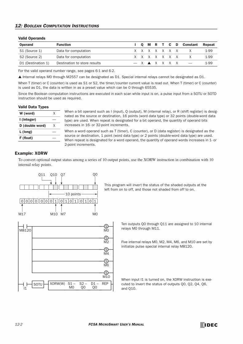
12: BOOLEAN COMPUTATION INSTRUCTIONS
Valid Operands
For the valid operand number range, see pages 6-1 and 6-2.
Internal relays M0 through M2557 can be designated as D1. Special internal relays cannot be designated as D1.
When T (timer) or C (counter) is used as S1 or S2, the timer/counter current value is read out. When T (timer) or C (counter) is used as D1, the data is written in as a preset value which can be 0 through 65535.
Since the Boolean computation instructions are executed in each scan while input is on, a pulse input from a SOTU or SOTD instruction should be used as required.
Valid Data Types
Example: XORWTo convert optional output status among a series of 10 output points, use the XORW instruction in combination with 10 internal relay points.
Operand Function I Q M R T C D Constant Repeat
S1 (Source 1) Data for computation X X X X X X X X 1-99
S2 (Source 2) Data for computation X X X X X X X X 1-99
D1 (Destination 1) Destination to store results — X X X X X — 1-99
W (word) X
I (integer) —
D (double word) X
L (long) —
F (float) —
When a bit operand such as I (input), Q (output), M (internal relay), or R (shift register) is desig-nated as the source or destination, 16 points (word data type) or 32 points (double-word data type) are used. When repeat is designated for a bit operand, the quantity of operand bits increases in 16- or 32-point increments.
When a word operand such as T (timer), C (counter), or D (data register) is designated as the source or destination, 1 point (word data type) or 2 points (double-word data type) are used. When repeat is designated for a word operand, the quantity of operand words increases in 1- or 2-point increments.
M8120
Ten outputs Q0 through Q11 are assigned to 10 internal relays M0 through M11.
Five internal relays M0, M2, M4, M6, and M10 are set by initialize pulse special internal relay M8120.
When input I1 is turned on, the XORW instruction is exe-cuted to invert the status of outputs Q0, Q2, Q4, Q6, and Q10.
0 0 00 0 0 1 10 0 1 0 1 0 1 0
Q0Q7Q10Q11
10 points
This program will invert the status of the shaded outputs at the left from on to off, and those not shaded from off to on.
REPS1 –M0
S2 –Q0
D1 –Q0
SOTUI1
M0M7M10M17
XORW(W)
M0S
M2S
M4S
M6S
M10S
12-2 FC5A MICROSMART USER’S MANUAL

12: BOOLEAN COMPUTATION INSTRUCTIONS
Repeat Operation in the ANDW, ORW, and XORW InstructionsSource operands S1 and S2 and destination operand D1 can be designated to repeat individually or in combination. When destination operand D1 is not designated to repeat, the final result is set to destination operand D1. When repeat is desig-nated, consecutive operands as many as the repeat cycles starting with the designated operand are used. Since the repeat operation works similarly on the ANDW (AND word), ORW (OR word), and XORW (exclusive OR word) instructions, the following examples are described using the ANDW instruction.
Repeat One Source Operand
• Data Type: WordWhen only S1 (source) is designated to repeat, the final result is set to destination operand D1.
• Data Type: Double WordWhen only S1 (source) is designated to repeat, the final result is set to destination operand D1·D1+1.
Repeat Destination Operand Only
• Data Type: WordWhen only D1 (destination) is designated to repeat, the same result is set to 3 operands starting with D1.
• Data Type: Double WordWhen only D1 (destination) is designated to repeat, the same result is set to 3 operands starting with D1·D1+1.
Repeat Two Source Operands
• Data Type: WordWhen S1 and S2 (source) are designated to repeat, the final result is set to destination operand D1.
• Data Type: Double WordWhen S1 and S2 (source) are designated to repeat, the final result is set to destination operand D1·D1+1.
I1 D10
S1 (Repeat = 3) D1 (Repeat = 0)S2 (Repeat = 0)
· (D30)D20
D11
D12
··
D20
D20
(D30)
D30
SOTU REP3
S1 RD10
D1 –D30
S2 –D20
ANDW(W)
D12·D13
D10·D11
D14·D15
S1 (Repeat = 3) D1 (Repeat = 0)S2 (Repeat = 0)
···
(D30·D31)
(D30·D31)
D30·D31
D20·D21
D20·D21
D20·D21
I1SOTU REP
3S1 RD10
D1 –D30
S2 –D20
ANDW(D)
I1REP3
S1 –D10
D1 RD30
S2 –D20
SOTU ANDW(W)D10
S1 (Repeat = 0) D1 (Repeat = 3)S2 (Repeat = 0)
· D30D20
D10
D10
··
D20
D20
D31
D32
I1REP3
S1 –D10
D1 RD30
D10·D11
D10·D11
D10·D11
S1 (Repeat = 0) D1 (Repeat = 3)S2 –D20
S2 (Repeat = 0)
···
D32·D33
D30·D31
D34·D35
D20·D21
D20·D21
D20·D21
SOTU ANDW(D)
I1REP3
D1 –D30
S2 RD20
SOTU D10
S1 (Repeat = 3) D1 (Repeat = 0)S2 (Repeat = 3)
· (D30)D20
D11
D12
··
D21
D22
(D30)
D30
S1 RD10
ANDW(W)
I1REP3
D1 –D30
D12·D13
D10·D11
D14·D15
S1 (Repeat = 3) D1 (Repeat = 0)S2 RD20
S2 (Repeat = 3)
···
(D30·D31)
(D30·D31)
D30·D31
D22·D23
D20·D21
D24·D25
SOTU S1 RD10
ANDW(D)
FC5A MICROSMART USER’S MANUAL 12-3
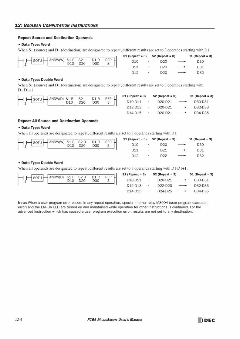
12: BOOLEAN COMPUTATION INSTRUCTIONS
Repeat Source and Destination Operands
• Data Type: WordWhen S1 (source) and D1 (destination) are designated to repeat, different results are set to 3 operands starting with D1.
• Data Type: Double WordWhen S1 (source) and D1 (destination) are designated to repeat, different results are set to 3 operands starting with D1·D1+1.
Repeat All Source and Destination Operands
• Data Type: WordWhen all operands are designated to repeat, different results are set to 3 operands starting with D1.
• Data Type: Double WordWhen all operands are designated to repeat, different results are set to 3 operands starting with D1·D1+1.
Note: When a user program error occurs in any repeat operation, special internal relay M8004 (user program execution error) and the ERROR LED are turned on and maintained while operation for other instructions is continued. For the advanced instruction which has caused a user program execution error, results are not set to any destination.
I1REP3
S1 RD10
D1 RD30
S2 –D20
SOTU ANDW(W) D10
S1 (Repeat = 3) D1 (Repeat = 3)S2 (Repeat = 0)
· D30D20
D11
D12
··
D20
D20
D31
D32
I1REP3
S1 RD10
D1 RD30
D12·D13
D10·D11
D14·D15
S1 (Repeat = 3) D1 (Repeat = 3)S2 –D20
S2 (Repeat = 0)
···
D32·D33
D30·D31
D34·D35
D20·D21
D20·D21
D20·D21
SOTU ANDW(D)
I1REP3
D1 RD30
S2 RD20
SOTU D10
S1 (Repeat = 3) D1 (Repeat = 3)S2 (Repeat = 3)
· D30D20
D11
D12
··
D21
D22
D31
D32
S1 RD10
ANDW(W)
I1REP3
D1 RD30
D12·D13
D10·D11
D14·D15
S1 (Repeat = 3) D1 (Repeat = 3)S2 RD20
S2 (Repeat = 3)
···
D32·D33
D30·D31
D34·D35
D22·D23
D20·D21
D24·D25
SOTU S1 RD10
ANDW(D)
12-4 FC5A MICROSMART USER’S MANUAL

13: SHIFT / ROTATE INSTRUCTIONS
IntroductionBit shift instructions are used to shift the data string starting with source operand S1 to the left or right by 1 to 15 bits as designated. The data string can be 1 to 65535 bits. The result is set to the source operand S1 and a carry (special internal relay M8003). The LSB or MSB is filled with 0 or 1 as designated.
Bit shift and rotate instructions are used to shift the 16- or 32-bit data string in the designated source operand S1 to the left or right by the quantity of bits designated. The result is set to the source operand S1 and a carry (special internal relay M8003).
The BCD left shift instruction shifts the BCD digits in two consecutive data registers to the left.
The word shift instruction is used to move 16-bit data to a destination data register and shifts down the data of subsequent data registers as many as designated.
SFTL (Shift Left)
Applicable CPU Modules
Valid Operands
For the valid operand number range, see pages 6-1 and 6-2.
Internal relays M0 through M2557 can be designated as S1. Special internal relays cannot be designated as S1.
Since the SFTL instruction is executed in each scan while input is on, a pulse input from a SOTU or SOTD instruction should be used as required.
FC5A-C10R2/C FC5A-C16R2/C FC5A-C24R2/C FC5A-D16RK1/RS1 FC5A-D32K3/S3
X X X X X
Operand Function I Q M R T C D Constant Repeat
S1 (Source 1) First data for bit shift — X X — — X — —
S2 (Source 2) Data to shift into the LSB X X X X — — — 0 or 1 —
N_B Number of bits in the data string — — — — — — X 1-65535 —
Bits Quantity of bits to shift — — — — — — — 1-15 —
S1*****
Bits**
CY ← S1
When input is on, N_B-bit data string starting with source operand S1 is shifted to the left by the quantity of bits designated by oper-and Bits.
The result is set to source operand S1, and the last bit status shifted out is set to a carry (special internal relay M8003). Zero or 1 designated by source operand S2 is set to the LSB.
0Before shift: 1 0 1010 1 0 1 1 1101 0 0CY
M8003
MSB LSBS1
1After shift: 00 1010 1 0 1 1 1101 0 0CY
M8003
MSB LSBS1
Shift to the left
SFTL
• S2 = 0, N_B = 16, Bits = 1
S2*****
N_B*****
S2
FC5A MICROSMART USER’S MANUAL 13-1

13: SHIFT / ROTATE INSTRUCTIONS
Examples: SFTL
• N_B = 16 bits
• N_B = 32 bits
M8120REP
M8120 is the initialize pulse special internal relay.
When the CPU starts operation, the MOV (move) instruc-tion sets 43690 to data register D10.
Each time input I0 is turned on, 16-bit data of data reg-ister D10 is shifted to the left by 1 bit as designated by operand Bits. The last bit status shifted out is set to a carry (special internal relay M8003). Zeros are set to the LSB.
0Before shift: D10 = 43690 1 1 1000 1 0 1 1 1000 1 0CY
M8003
MSB LSBD10
1After first shift: D10 = 21844 01 1000 1 0 1 1 1000 1 0CY
M8003
MSB LSBD10
Bits to shift = 1
SOTUI0
S1 –43690
D1 –D10
S1D10
Bits1
0
00 0111 0 1 0 0 0111 0 00After second shift: D10 = 43688CY
M8003
MSB LSBD10
SFTL
MOV(W)
Shift to the left
S20
N_B16
S2
M8120 is the initialize pulse special internal relay.
When the CPU starts operation, the MOV (move) instruc-tions set 0 and 65535 to data registers D10 and D11, respectively.
Each time input I0 is turned on, 32-bit data of data reg-isters D10 and D11 is shifted to the left by 2 bits as designated by operand Bits. D10 is the low word, and D11 is the high word.
The last bit status shifted out is set to a carry (special internal relay M8003). Ones are set to the LSBs.
Bits to shift = 2
1
Before shift:
0 0 0000 0 0 0 0 0000 0 0CY
M8003
MSB LSBD11
1
After shift:
10 0000 0 0 0 0 0000 0 1CY
M8003
MSB LSBD10
Shift to the left
01 1111 1 1 1 1 1111 1 0
1 1 1111 1 1 1 1 1111 1 1
M8120REP
SOTUI0
S1 –0
D1 –D10
S1D10
Bits2
SFTL
MOV(W)
S21
N_B32
REPS1 –65535
D1 –D11
MOV(W)
D10 S2
D11
13-2 FC5A MICROSMART USER’S MANUAL

13: SHIFT / ROTATE INSTRUCTIONS
SFTR (Shift Right)
Applicable CPU Modules
Valid Operands
For the valid operand number range, see pages 6-1 and 6-2.
Since the SFTR instruction is executed in each scan while input is on, a pulse input from a SOTU or SOTD instruction should be used as required.
FC5A-C10R2/C FC5A-C16R2/C FC5A-C24R2/C FC5A-D16RK1/RS1 FC5A-D32K3/S3
X X X X X
Operand Function I Q M R T C D Constant Repeat
S1 (Source 1) First data for bit shift — X X — — X — —
S2 (Source 2) Data to shift into the MSB X X X X — — — 0 or 1 —
N_B Number of bits in the data string — — — — — — X 1-65535 —
Bits Quantity of bits to shift — — — — — — — 1-15 —
S1 → CY
When input is on, N_B-bit data string starting with source oper-and S1 is shifted to the right by the quantity of bits designated by operand Bits.
The result is set to source operand S1, and the last bit status shifted out is set to a carry (special internal relay M8003). Zero or 1 designated by source operand S2 is set to the MSB.
0Before shift: 1 0 1010 1 0 1 1 1101 0 0CY
M8003
MSB LSBS1
0After shift: 11 1100 0 0 1 1 0010 1 1CY
M8003
MSB LSBS1
Shift to the right
• S2 = 0, N_B = 16, Bits = 1S2
S1*****
Bits**
SFTR S2*****
N_B*****
FC5A MICROSMART USER’S MANUAL 13-3
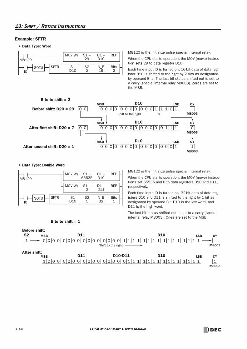
13: SHIFT / ROTATE INSTRUCTIONS
Example: SFTR
• Data Type: Word
• Data Type: Double Word
M8120REP
M8120 is the initialize pulse special internal relay.
When the CPU starts operation, the MOV (move) instruc-tion sets 29 to data register D10.
Each time input I0 is turned on, 16-bit data of data reg-ister D10 is shifted to the right by 2 bits as designated by operand Bits. The last bit status shifted out is set to a carry (special internal relay M8003). Zeros are set to the MSB.
SOTUI0
S1 –29
D1 –D10
S1D10
Bits2
SFTR
MOV(W)
0Before shift: D20 = 29 0 0 0000 0 0 0 0 0110 1 1CY
M8003
MSB LSBD10
0After first shift: D20 = 7 10 0000 0 0 0 0 1000 0 1CY
M8003
MSB LSBD10
Bits to shift = 2
0
10 0000 0 0 0 0 0000 0 0After second shift: D20 = 1CY
M8003
MSB LSBD101
0
0
Shift to the right
S20
N_B16
M8120 is the initialize pulse special internal relay.
When the CPU starts operation, the MOV (move) instruc-tions set 65535 and 0 to data registers D10 and D11, respectively.
Each time input I0 is turned on, 32-bit data of data reg-isters D10 and D11 is shifted to the right by 1 bit as designated by operand Bit. D10 is the low word, and D11 is the high word.
The last bit status shifted out is set to a carry (special internal relay M8003). Ones are set to the MSB.
Bits to shift = 1
1
Before shift:
1 1 1111 1 1 1 1 1111 1 1CY
M8003
MSB LSBD10
1
After shift:
11 1110 1 1 1 1 1111 1 1CY
M8003
MSB LSBD10·D11
Shift to the right
00 0001 0 0 0 0 0000 0 0
0 0 0000 0 0 0 0 0000 0 0
M8120REP
SOTUI0
S1 –65535
D1 –D10
S1D10
Bits1
SFTR
MOV(W)
S21
N_B32
REPS1 –0
D1 –D11
MOV(W)
D11
D11 D10
S2
13-4 FC5A MICROSMART USER’S MANUAL

13: SHIFT / ROTATE INSTRUCTIONS
BCDLS (BCD Left Shift)
Applicable CPU Modules
Valid Operands
For the valid operand number range, see pages 6-1 and 6-2.
When T (timer) or C (counter) is used as S2, the timer/counter current value is read out.
The quantity of digits to shift designated as S2 can be 1 through 7.
Make sure that the source data determined by S1 and S1+1 is between 0 and 9999 for each data register. If either source data is over 9999, a user program execution error will result, turning on special internal relay M8004 and the ERR LED on the CPU module. When S2 is over 7, a user program execution error will also result.
Valid Data Types
FC5A-C10R2/C FC5A-C16R2/C FC5A-C24R2/C FC5A-D16RK1/RS1 FC5A-D32K3/S3
X X X X X
Operand Function I Q M R T C D Constant Repeat
S1 (Source 1) Data for BCD shift — — — — — — X — —
S2 (Source 2) Quantity of digits to shift X X X X X X X 1-7 —
W (word) —
I (integer) —
D (double word) X
L (long) —
F (float) —
When input is on, the 32-bit binary data designated by S1 is converted into 8 BCD digits, shifted to the left by the quantity of digits designated by S2, and con-verted back to 32-bit binary data.
Valid values for each of S1 and S1+1 are 0 through 9999.
The quantity of digits to shift can be 1 through 7.
Zeros are set to the lowest digits as many as the digits shifted.
BCDLS S1*****
Before shift:
After shift:
0 2 31
MSD
S1 S1+1
Shift to the left
LSD
S2*
4 6 75 0
1 3 42 5 7 060
When S2 = 1 (digits to shift)
0
When a word operand such as D (data register) is designated as source S1, 2 points (double-word data type) are used.
When a bit operand such as I (input), Q (output), M (internal relay), or R (shift register) is desig-nated as source S2, 16 points are used.
When a word operand such as T (timer), C (counter), or D (data register) is designated as source S2, 1 point is used.
FC5A MICROSMART USER’S MANUAL 13-5

13: SHIFT / ROTATE INSTRUCTIONS
Example: BCDLS
M8120 is the initialize pulse special internal relay.
When the CPU starts operation, the MOV (move) instructions set 123 and 4567 to data registers D10 and D11, respectively.
Each time input I0 is turned on, the 32-bit binary data of data registers D10 and D11 designated by S1 is converted into 8 BCD digits, shifted to the left by 1 digit as designated by operand S2, and converted back to 32-bit binary data.
Zeros are set to the lowest digits as many as the digits shifted.
Before shift:
After first shift:
0 2 31D10 D11
Shift to the left
4 6 75 0
1 3 42 5 7 060
REP
SOTUI0
S1 –4567
D1 –D11
S1D10
S21
BCDLS
MOV(W)
M8120REPS1 –
123D1 –D10
MOV(W)
After second shift:MSD LSD2 4 53 6 0 071
0
When S2 = 1 (digits to shift)
13-6 FC5A MICROSMART USER’S MANUAL

13: SHIFT / ROTATE INSTRUCTIONS
WSFT (Word Shift)
Applicable CPU Modules
Valid Operands
For the valid operand number range, see pages 6-1 and 6-2.
When T (timer) or C (counter) is used as S1 or S2, the timer/counter current value is read out.
Valid Data Types
Special Internal Relay M8024: BMOV/WSFT Executing FlagWhile the BMOV or WSFT is executed, M8024 turns on. When completed, M8024 turns off. If the CPU is powered down while executing BMOV or WSFT, M8024 remains on when the CPU is powered up again.
Example: WSFT
FC5A-C10R2/C FC5A-C16R2/C FC5A-C24R2/C FC5A-D16RK1/RS1 FC5A-D32K3/S3
X X X X X
Operand Function I Q M R T C D Constant Repeat
S1 (Source 1) Source data for word shift X X X X X X X X —
S2 (Source 2) Quantity of blocks to shift X X X X X X X X —
D1 (Destination 1) First operand number to shift — — — — — — X — —
W (word) X
I (integer) —
D (double word) —
L (long) —
F (float) —
When input is on, N blocks of 16-bit word data starting with operand designated by D1 are shifted up to the next 16-bit positions. At the same time, the data designated by operand S1 is moved to operand designated by D1. S2 specifies the quantity of blocks to move.
WSFT S1*****
D1*****
S2*****
When S2 = 3 (quantity of blocks to shift)
First 16-bit dataD1+0
Second 16-bit dataD1+1
Third 16-bit dataD1+2
Fifth 16-bit dataD1+4
Fourth 16-bit dataD1+3
S1 dataD1+0
First 16-bit dataD1+1
Second 16-bit dataD1+2
Fifth 16-bit dataD1+4
Third 16-bit dataD1+33 blocks (S2)
16-bit dataS1 16-bit dataS1
When a bit operand such as I (input), Q (output), M (internal relay), or R (shift register) is desig-nated as source S1 or S2, 16 points are used.
When a word operand such as T (timer), C (counter), or D (data register) is designated as source S1 or S2, 1 point is used.
D100 through D102 → D101 through D103
D10 → D100
When input I0 is turned on, data of 3 data registers starting with D100 designated by destination operand D1 is shifted to the next data registers. Data of data register D10 designated by source oper-and S1 is moved to D100 designated by destination operand D1.
SOTUI0
S1D10
D1D100
WSFT S23
2222D101
1111D100
3333D102
4444D103
5555D104
1111D101
12345D100
2222D102
3333D103
5555D104
12345D10 12345D10
Before shift: After first shift:
FC5A MICROSMART USER’S MANUAL 13-7

13: SHIFT / ROTATE INSTRUCTIONS
ROTL (Rotate Left)
Applicable CPU Modules
Valid Operands
For the valid operand number range, see pages 6-1 and 6-2.
Internal relays M0 through M2557 can be designated as S1. Special internal relays cannot be designated as S1.
The quantity of bits to rotate can be 1 through 15 for the word data type, or 1 through 31 for the double-word data type.
Since the ROTL instruction is executed in each scan while input is on, a pulse input from a SOTU or SOTD instruction should be used as required.
Valid Data Types
FC5A-C10R2/C FC5A-C16R2/C FC5A-C24R2/C FC5A-D16RK1/RS1 FC5A-D32K3/S3
X X X X X
Operand Function I Q M R T C D Constant Repeat
S1 (Source 1) Data for bit rotation — X X — — X — —
bits Quantity of bits to rotate — — — — — — — 1-15, 1-31 —
W (word) X
I (integer) —
D (double word) X
L (long) —
F (float) —
Before rotation: 1 0 1010 1 0 1 1 1101 0 0CY
M8003
MSB LSBS1
1After rotation: 0 1010 1 0 1 1 1101 0 0CY
M8003
MSB LSBS11
Rotate to the left
S1*****
bits**
When input is on, 16- or 32-bit data of the designated source operand S1 is rotated to the left by the quantity of bits designated by operand bits.
The result is set to the source operand S1, and the last bit status rotated out is set to a carry (special internal relay M8003).
ROTL(*)
• Data Type: Word (bits to rotate = 1)
Before rotation:
1 0 1010 1 0 1 1 1101 0 0CY
M8003
MSB LSBS1
1
After rotation:
10 1010 1 0 1 1 1101 0 0CY
M8003
MSB LSBS1
Rotate to the left
10 1010 1 0 1 1 1101 0 0
1 0 1010 1 0 1 1 1101 0 0
• Data Type: Double Word (bits to rotate = 1)
When a bit operand such as Q (output), M (internal relay), or R (shift register) is designated as the source, 16 points (word data type) or 32 points (double-word data type) are used.
When a word operand such as D (data register) is designated as the source, 1 point (word data type) or 2 points (double-word data type) are used.
13-8 FC5A MICROSMART USER’S MANUAL

13: SHIFT / ROTATE INSTRUCTIONS
Example: ROTL
• Data Type: Word
• Data Type: Double Word
Before rotation: D10 = 40966 1 1 0000 0 0 0 0 1100 0 0CY
M8003
MSB LSBD10
After first rotation: D10 = 16397
Bits to rotate = 1
After second rotation: D10 = 32794
1 0 0 0001 0 0 0 0 0100 1 1CY
M8003
MSB LSBD10
0 1 0 0000 0 0 0 0 1010 1 0CY
M8003
MSB LSBD10
M8120REP
M8120 is the initialize pulse special internal relay.
When the CPU starts operation, the MOV (move) instruction sets 40966 to data register D10.
Each time input I0 is turned on, 16-bit data of data register D10 is rotated to the left by 1 bit as designated by operand bits.
The status of the MSB is set to a carry (special internal relay M8003).
SOTUI0
S1 –40966
D1 –D10
S1D10
bits1
ROTL(W)
MOV(W)
Each time input I1 is turned on, 32-bit data of data registers D10 and D11 is rotated to the left by 1 bit as designated by operand bits.
The status of the MSB is set to a carry (special internal relay M8003).
Bits to rotate = 1
SOTUI1
S1D10
bits1
ROTL(D)
Before rotation: D10·D11 = 2,684,788,742
After rotation: D10·D11 = 1,074,610,189
1 1 0000 0 0 0 0 1100 0 0CY
M8003
MSB LSBD10·D11
1 11 0000 0 0 0 0 1100 0 0CY
M8003
MSB LSBD10·D11
Rotate to the left
11 0000 0 0 0 0 1100 0 0
1 1 0000 0 0 0 0 1100 0 0
FC5A MICROSMART USER’S MANUAL 13-9

13: SHIFT / ROTATE INSTRUCTIONS
ROTR (Rotate Right)
Applicable CPU Modules
Valid Operands
For the valid operand number range, see pages 6-1 and 6-2.
Internal relays M0 through M2557 can be designated as S1. Special internal relays cannot be designated as S1.
The quantity of bits to rotate can be 1 through 15 for the word data type, or 1 through 31 for the double-word data type.
Since the ROTR instruction is executed in each scan while input is on, a pulse input from a SOTU or SOTD instruction should be used as required.
Valid Data Types
FC5A-C10R2/C FC5A-C16R2/C FC5A-C24R2/C FC5A-D16RK1/RS1 FC5A-D32K3/S3
X X X X X
Operand Function I Q M R T C D Constant Repeat
S1 (Source 1) Data for bit rotation — X X — — X — —
bits Quantity of bits to rotate — — — — — — — 1-15, 1-31 —
W (word) X
I (integer) —
D (double word) X
L (long) —
F (float) —
Before rotation: 1 0 1010 1 0 1 1 1101 0 0CY
M8003
MSB LSBS1
0After rotation: 1 1100 0 0 1 1 0010 1 1CY
M8003
MSB LSBS11
Rotate to the right
S1*****
bits**
When input is on, 16- or 32-bit data of the designated source operand S1 is rotated to the right by the quantity of bits designated by operand bits.
The result is set to the source operand S1, and the last bit status rotated out is set to a carry (special internal relay M8003).
ROTR(*)
• Data Type: Word (bits to rotate = 1)
Before rotation:
1 0 1010 1 0 1 1 1101 0 0CY
M8003
MSB LSBS1
0
After rotation:CY
M8003
MSB LSBS1
Rotate to the right1 0 1010 1 0 1 1 1101 0 0
• Data Type: Double Word (bits to rotate = 1)
1 1100 0 0 1 1 0010 1 1 1 1 1100 0 0 1 1 0010 1 1 1
When a bit operand such as Q (output), M (internal relay), or R (shift register) is designated as the source, 16 points (word data type) or 32 points (double-word data type) are used.
When a word operand such as D (data register) is designated as the source, 1 point (word data type) or 2 points (double-word data type) are used.
13-10 FC5A MICROSMART USER’S MANUAL

13: SHIFT / ROTATE INSTRUCTIONS
Example: ROTR
• Data Type: Word
• Data Type: Double Word
Before rotation: D20 = 13 0 0 0000 0 0 0 0 0100 1 1CY
M8003
MSB LSBD20
After first rotation: D20 = 16387
Bits to rotate = 2
After second rotation: D20 = 53248
00 0 0001 0 0 0 0 1000 0 1CY
M8003
MSB LSBD20
11 0 0011 0 0 0 0 0000 0 0CY
M8003
MSB LSBD20
M8120REP
M8120 is the initialize pulse special internal relay.
When the CPU starts operation, the MOV (move) instruction sets 13 to data register D20.
Each time input I1 is turned on, 16-bit data of data register D20 is rotated to the right by 2 bits as designated by operand bits.
The last bit status rotated out is set to a carry (special internal relay M8003).
SOTUI1
S1 –13
D1 –D20
S1D20
bits2
ROTR(W)
MOV(W)
Each time input I1 is turned on, 32-bit data of data registers D20 and D21 is rotated to the right by 1 bit as designated by operand bits.
The last bit status rotated out is set to a carry (special internal relay M8003).
Bits to rotate = 1
SOTUI1
S1D20
bits1
ROTR(D)
Before rotation: D20·D21 = 851,981
After rotation: D20·D21 = 2,147,909,638
0 0 0000 0 0 0 0 0100 1 1CY
M8003
MSB LSBD20·D21
1CY
M8003
MSB LSBD20·D21
Rotate to the right0 0 0000 0 0 0 0 0100 1 1
0 0001 0 0 0 0 1000 0 1 0 0 0001 0 0 0 0 1000 0 1 0
FC5A MICROSMART USER’S MANUAL 13-11

13: SHIFT / ROTATE INSTRUCTIONS
13-12 FC5A MICROSMART USER’S MANUAL
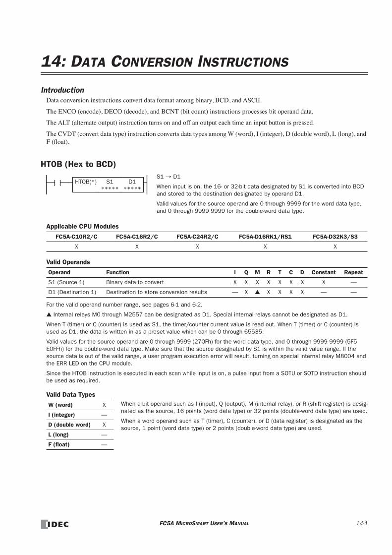
14: DATA CONVERSION INSTRUCTIONS
IntroductionData conversion instructions convert data format among binary, BCD, and ASCII.
The ENCO (encode), DECO (decode), and BCNT (bit count) instructions processes bit operand data.
The ALT (alternate output) instruction turns on and off an output each time an input button is pressed.
The CVDT (convert data type) instruction converts data types among W (word), I (integer), D (double word), L (long), and F (float).
HTOB (Hex to BCD)
Applicable CPU Modules
Valid Operands
For the valid operand number range, see pages 6-1 and 6-2.
Internal relays M0 through M2557 can be designated as D1. Special internal relays cannot be designated as D1.
When T (timer) or C (counter) is used as S1, the timer/counter current value is read out. When T (timer) or C (counter) is used as D1, the data is written in as a preset value which can be 0 through 65535.
Valid values for the source operand are 0 through 9999 (270Fh) for the word data type, and 0 through 9999 9999 (5F5 E0FFh) for the double-word data type. Make sure that the source designated by S1 is within the valid value range. If the source data is out of the valid range, a user program execution error will result, turning on special internal relay M8004 and the ERR LED on the CPU module.
Since the HTOB instruction is executed in each scan while input is on, a pulse input from a SOTU or SOTD instruction should be used as required.
Valid Data Types
FC5A-C10R2/C FC5A-C16R2/C FC5A-C24R2/C FC5A-D16RK1/RS1 FC5A-D32K3/S3
X X X X X
Operand Function I Q M R T C D Constant Repeat
S1 (Source 1) Binary data to convert X X X X X X X X —
D1 (Destination 1) Destination to store conversion results — X X X X X — —
W (word) X
I (integer) —
D (double word) X
L (long) —
F (float) —
S1 → D1
When input is on, the 16- or 32-bit data designated by S1 is converted into BCD and stored to the destination designated by operand D1.
Valid values for the source operand are 0 through 9999 for the word data type, and 0 through 9999 9999 for the double-word data type.
HTOB(*) S1*****
D1*****
When a bit operand such as I (input), Q (output), M (internal relay), or R (shift register) is desig-nated as the source, 16 points (word data type) or 32 points (double-word data type) are used.
When a word operand such as T (timer), C (counter), or D (data register) is designated as the source, 1 point (word data type) or 2 points (double-word data type) are used.
FC5A MICROSMART USER’S MANUAL 14-1

14: DATA CONVERSION INSTRUCTIONS
Examples: HTOB
• Data Type: Word
• Data Type: Double Word
D1D20
S1D10I1
HTOB(W)Binary
SOTU 0D10 (0000h)
BCD
0D20 (0000h)
1234D10 (04D2h)4660D20 (1234h)
9999D10 (270Fh)39321D20 (9999h)
D1D20
S1D10I2
HTOB(D)SOTU 0D10 (0000h)0D11 (0000h)
0D20 (0000h)0D21 (0000h)
Binary BCD
188D10 (00BCh)24910D11 (614Eh)
4660D20 (1234h)22136D21 (5678h)
1525D10 (05F5h)57599D11 (E0FFh)
39321D20 (9999h)39321D21 (9999h)
14-2 FC5A MICROSMART USER’S MANUAL

14: DATA CONVERSION INSTRUCTIONS
BTOH (BCD to Hex)
Applicable CPU Modules
Valid Operands
For the valid operand number range, see pages 6-1 and 6-2.
Internal relays M0 through M2557 can be designated as D1. Special internal relays cannot be designated as D1.
When T (timer) or C (counter) is used as S1, the timer/counter current value is read out. When T (timer) or C (counter) is used as D1, the data is written in as a preset value which can be 0 through 65535.
Valid values for the source operand are 0 through 9999 (BCD) for the word data type, and 0 through 9999 9999 (BCD) for the double-word data type. Make sure that each digit of the source designated by S1 is 0 through 9. If the source data is out of the valid range, a user program execution error will result, turning on special internal relay M8004 and the ERR LED on the CPU module.
Since the BTOH instruction is executed in each scan while input is on, a pulse input from a SOTU or SOTD instruction should be used as required.
Valid Data Types
FC5A-C10R2/C FC5A-C16R2/C FC5A-C24R2/C FC5A-D16RK1/RS1 FC5A-D32K3/S3
X X X X X
Operand Function I Q M R T C D Constant Repeat
S1 (Source 1) BCD data to convert X X X X X X X X —
D1 (Destination 1) Destination to store conversion results — X X X X X — —
W (word) X
I (integer) —
D (double word) X
L (long) —
F (float) —
S1 → D1
When input is on, the BCD data designated by S1 is converted into 16- or 32-bit binary data and stored to the destination designated by operand D1.
Valid values for the source operand are 0 through 9999 (BCD) for the word data type, and 0 through 9999 9999 (BCD) for the double-word data type.
BTOH(*) S1*****
D1*****
When a bit operand such as I (input), Q (output), M (internal relay), or R (shift register) is desig-nated as the source, 16 points (word data type) or 32 points (double-word data type) are used.
When a word operand such as T (timer), C (counter), or D (data register) is designated as the source, 1 point (word data type) or 2 points (double-word data type) are used.
FC5A MICROSMART USER’S MANUAL 14-3

14: DATA CONVERSION INSTRUCTIONS
Examples: BTOH
• Data Type: Word
• Data Type: Double Word
D1D20
S1D10I1
BTOH(W)BCD
SOTU 0D10 (0000h)
Binary
0D20 (0000h)
4660D10 (1234h)1234D20 (04D2h)
39321D10 (9999h)9999D20 (270Fh)
D1D20
S1D10I2
BTOH(D)SOTU 0D10 (0000h)0D11 (0000h)
0D20 (0000h)0D21 (0000h)
BCD Binary
188D10 (00BCh)24910D11 (614Eh)
4660 D20(1234h)22136 D21(5678h)
1525D10 (05F5h)57599D11 (E0FFh)
39321 D20(9999h)39321 D21(9999h)
14-4 FC5A MICROSMART USER’S MANUAL

14: DATA CONVERSION INSTRUCTIONS
HTOA (Hex to ASCII)
Applicable CPU Modules
Valid Operands
For the valid operand number range, see pages 6-1 and 6-2.
When T (timer) or C (counter) is used as S1 or S2, the timer/counter current value is read out.
The quantity of digits to convert can be 1 through 4. Make sure that the quantity of digits designated by S2 is within the valid range. If the S2 data is out of the valid range, a user program execution error will result, turning on special internal relay M8004 and the ERR LED on the CPU module.
Since the HTOA instruction is executed in each scan while input is on, a pulse input from a SOTU or SOTD instruction should be used as required.
Valid Data Types
FC5A-C10R2/C FC5A-C16R2/C FC5A-C24R2/C FC5A-D16RK1/RS1 FC5A-D32K3/S3
X X X X X
Operand Function I Q M R T C D Constant Repeat
S1 (Source 1) Binary data to convert X X X X X X X X —
S2 (Source 2) Quantity of digits to convert X X X X X X X 1-4 —
D1 (Destination 1) Destination to store conversion results — — — — — — X — —
W (word) X
I (integer) —
D (double word) —
L (long) —
F (float) —
S1 → D1, D1+1, D1+2, D1+3
When input is on, the 16-bit binary data designated by S1 is read from the lowest digit as many as the quantity of digits designated by S2, con-verted into ASCII data, and stored to the destination starting with the operand designated by D1.
The quantity of digits to convert can be 1 through 4.
HTOA(W) S1*****
S2*****
D1*****
When a bit operand such as I (input), Q (output), M (internal relay), or R (shift register) is desig-nated as the source, 16 points (word data type) are used.
When a word operand such as T (timer), C (counter), or D (data register) is designated as the source or destination, 1 point (word data type) is used.
FC5A MICROSMART USER’S MANUAL 14-5

14: DATA CONVERSION INSTRUCTIONS
Examples: HTOA
• Quantity of Digits: 4
• Quantity of Digits: 3
• Quantity of Digits: 2
• Quantity of Digits: 1
D1D20
S1D10I0
HTOA(W) S24
SOTU
Binary
4660D10 (1234h)
ASCII
49D20 (0031h)
50D21 (0032h)
51D22 (0033h)
52D23 (0034h)
D1D20
S1D10I1
HTOA(W) S23
SOTU
Binary
4660D10 (1234h)
ASCII
50D20 (0032h)
51D21 (0033h)
52D22 (0034h)
D1D20
S1D10I2
HTOA(W) S22
SOTU
Binary
4660D10 (1234h)
ASCII
51D20 (0033h)
52D21 (0034h)
D1D20
S1D10I3
HTOA(W) S21
SOTU
Binary
4660D10 (1234h)
ASCII
52D20 (0034h)
14-6 FC5A MICROSMART USER’S MANUAL

14: DATA CONVERSION INSTRUCTIONS
ATOH (ASCII to Hex)
Applicable CPU Modules
Valid Operands
For the valid operand number range, see pages 6-1 and 6-2.
Internal relays M0 through M2557 can be designated as D1. Special internal relays cannot be designated as D1.
When T (timer) or C (counter) is used as S2, the timer/counter current value is read out. When T (timer) or C (counter) is used as D1, the data is written in as a preset value which can be 0 through 65535.
Valid values for source S1 data to convert are 30h to 39h and 41h to 46h. Make sure that the values for each source desig-nated by S1 and the quantity of digits designated by S2 are within the valid range. If the S1 or S2 data is out of the valid range, a user program execution error will result, turning on special internal relay M8004 and the ERR LED on the CPU mod-ule.
Since the ATOH instruction is executed in each scan while input is on, a pulse input from a SOTU or SOTD instruction should be used as required.
Valid Data Types
FC5A-C10R2/C FC5A-C16R2/C FC5A-C24R2/C FC5A-D16RK1/RS1 FC5A-D32K3/S3
X X X X X
Operand Function I Q M R T C D Constant Repeat
S1 (Source 1) ASCII data to convert — — — — — — X — —
S2 (Source 2) Quantity of digits to convert X X X X X X X 1-4 —
D1 (Destination 1) Destination to store conversion results — X X X X X — —
W (word) X
I (integer) —
D (double word) —
L (long) —
F (float) —
S1, S1+1, S1+2, S1+3 → D1
When input is on, the ASCII data designated by S1 as many as the quan-tity of digits designated by S2 is converted into 16-bit binary data, and stored to the destination designated by operand D1.
Valid values for source data to convert are 30h to 39h and 41h to 46h.
The quantity of digits to convert can be 1 through 4.
ATOH(W) S1*****
S2*****
D1*****
When a bit operand such as I (input), Q (output), M (internal relay), or R (shift register) is desig-nated as the source or destination, 16 points (word data type) are used.
When a word operand such as T (timer), C (counter), or D (data register) is designated as the source or destination, 1 point (word data type) is used.
FC5A MICROSMART USER’S MANUAL 14-7

14: DATA CONVERSION INSTRUCTIONS
Examples: ATOH
• Quantity of Digits: 4
• Quantity of Digits: 3
• Quantity of Digits: 2
• Quantity of Digits: 1
D1D20
S1D10I0
ATOH(W) S24
SOTU
Binary
4660D20 (1234h)
ASCII
49D10 (0031h)
50D11 (0032h)
51D12 (0033h)
52D13 (0034h)
D1D20
S1D10I1
ATOH(W) S23
SOTU
Binary
291D20 (0123h)
ASCII
49D10 (0031h)
50D11 (0032h)
51D12 (0033h)
D1D20
S1D10I2
ATOH(W) S22
SOTU
Binary
18D20 (0012h)
ASCII
49D10 (0031h)
50D11 (0032h)
D1D20
S1D10I3
ATOH(W) S21
SOTU
Binary
1D20 (0001h)
ASCII
49D10 (0031h)
14-8 FC5A MICROSMART USER’S MANUAL

14: DATA CONVERSION INSTRUCTIONS
BTOA (BCD to ASCII)
Applicable CPU Modules
Valid Operands
For the valid operand number range, see pages 6-1 and 6-2.
When T (timer) or C (counter) is used as S1 or S2, the timer/counter current value is read out.
The quantity of digits to convert can be 1 through 5. Make sure that the quantity of digits designated by S2 is within the valid range. If the S2 data is out of the valid range, a user program execution error will result, turning on special internal relay M8004 and the ERR LED on the CPU module.
Since the BTOA instruction is executed in each scan while input is on, a pulse input from a SOTU or SOTD instruction should be used as required.
Valid Data Types
FC5A-C10R2/C FC5A-C16R2/C FC5A-C24R2/C FC5A-D16RK1/RS1 FC5A-D32K3/S3
X X X X X
Operand Function I Q M R T C D Constant Repeat
S1 (Source 1) Binary data to convert X X X X X X X X —
S2 (Source 2) Quantity of digits to convert X X X X X X X 1-5 —
D1 (Destination 1) Destination to store conversion results — — — — — — X — —
W (word) X
I (integer) —
D (double word) —
L (long) —
F (float) —
S1 → D1, D1+1, D1+2, D1+3, D1+4
When input is on, the 16-bit binary data designated by S1 is converted into BCD, and converted into ASCII data. The data is read from the low-est digit as many as the quantity of digits designated by S2. The result is stored to the destination starting with the operand designated by D1.
The quantity of digits to convert can be 1 through 5.
BTOA(W) S1*****
S2*****
D1*****
When a bit operand such as I (input), Q (output), M (internal relay), or R (shift register) is desig-nated as the source, 16 points (word data type) are used.
When a word operand such as T (timer), C (counter), or D (data register) is designated as the source or destination, 1 point (word data type) is used.
FC5A MICROSMART USER’S MANUAL 14-9

14: DATA CONVERSION INSTRUCTIONS
Examples: BTOA
• Quantity of Digits: 5
• Quantity of Digits: 4
• Quantity of Digits: 3
• Quantity of Digits: 2
• Quantity of Digits: 1
D1D20
S1D10I0
BTOA(W) S25
SOTU
BCD
12345D10 (3039h)
ASCII
49D20 (0031h)
50D21 (0032h)
51D22 (0033h)
52D23 (0034h)
Binary
53D24 (0035h)
D1D20
S1D10I1
BTOA(W) S24
SOTU
BCD
12345D10 (3039h)
ASCII
50D20 (0032h)
51D21 (0033h)
52D22 (0034h)
53D23 (0035h)
Binary
D1D20
S1D10I2
BTOA(W) S23
SOTU
BCD
12345D10 (3039h)
ASCII
51D20 (0033h)
52D21 (0034h)
53D22 (0035h)
Binary
D1D20
S1D10I3
BTOA(W) S22
SOTU
BCD
12345D10 (3039h)
ASCII
52D20 (0034h)
53D21 (0035h)
Binary
D1D20
S1D10I4
BTOA(W) S21
SOTU
BCD
12345D10 (3039h)
ASCII
53D20 (0035h)
Binary
14-10 FC5A MICROSMART USER’S MANUAL
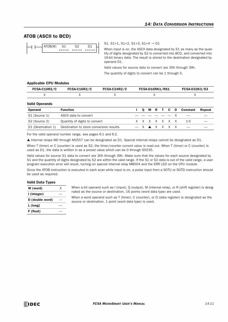
14: DATA CONVERSION INSTRUCTIONS
ATOB (ASCII to BCD)
Applicable CPU Modules
Valid Operands
For the valid operand number range, see pages 6-1 and 6-2.
Internal relays M0 through M2557 can be designated as D1. Special internal relays cannot be designated as D1.
When T (timer) or C (counter) is used as S2, the timer/counter current value is read out. When T (timer) or C (counter) is used as D1, the data is written in as a preset value which can be 0 through 65535.
Valid values for source S1 data to convert are 30h through 39h. Make sure that the values for each source designated by S1 and the quantity of digits designated by S2 are within the valid range. If the S1 or S2 data is out of the valid range, a user program execution error will result, turning on special internal relay M8004 and the ERR LED on the CPU module.
Since the ATOB instruction is executed in each scan while input is on, a pulse input from a SOTU or SOTD instruction should be used as required.
Valid Data Types
FC5A-C10R2/C FC5A-C16R2/C FC5A-C24R2/C FC5A-D16RK1/RS1 FC5A-D32K3/S3
X X X X X
Operand Function I Q M R T C D Constant Repeat
S1 (Source 1) ASCII data to convert — — — — — — X — —
S2 (Source 2) Quantity of digits to convert X X X X X X X 1-5 —
D1 (Destination 1) Destination to store conversion results — X X X X X — —
W (word) X
I (integer) —
D (double word) —
L (long) —
F (float) —
S1, S1+1, S1+2, S1+3, S1+4 → D1
When input is on, the ASCII data designated by S1 as many as the quan-tity of digits designated by S2 is converted into BCD, and converted into 16-bit binary data. The result is stored to the destination designated by operand D1.
Valid values for source data to convert are 30h through 39h.
The quantity of digits to convert can be 1 through 5.
ATOB(W) S1*****
S2*****
D1*****
When a bit operand such as I (input), Q (output), M (internal relay), or R (shift register) is desig-nated as the source or destination, 16 points (word data type) are used.
When a word operand such as T (timer), C (counter), or D (data register) is designated as the source or destination, 1 point (word data type) is used.
FC5A MICROSMART USER’S MANUAL 14-11

14: DATA CONVERSION INSTRUCTIONS
Examples: ATOB
• Quantity of Digits: 5
• Quantity of Digits: 4
• Quantity of Digits: 3
• Quantity of Digits: 2
• Quantity of Digits: 1
D1D20
S1D10I0
ATOB(W) S25
SOTU
BCD
12345D20 (3039h)
ASCII
49D10 (0031h)
50D11 (0032h)
51D12 (0033h)
52D13 (0034h)
Binary
53D14 (0035h)
D1D20
S1D10I1
ATOB(W) S24
SOTU
BCD
1234D20 (04D2h)
ASCII
49D10 (0031h)
50D11 (0032h)
51D12 (0033h)
52D13 (0034h)
Binary
D1D20
S1D10I2
ATOB(W) S23
SOTU
BCD
123D20 (007Bh)
ASCII
49D10 (0031h)
50D11 (0032h)
51D12 (0033h)
Binary
D1D20
S1D10I3
ATOB(W) S22
SOTU
BCD
12D20 (0018h)
ASCII
49D10 (0031h)
50D11 (0032h)
Binary
D1D20
S1D10I4
ATOB(W) S21
SOTU
BCD
1D20 (0001h)
ASCII
49D10 (0031h)
Binary
14-12 FC5A MICROSMART USER’S MANUAL

14: DATA CONVERSION INSTRUCTIONS
ENCO (Encode)
Applicable CPU Modules
Valid Operands
For the valid operand number range, see pages 6-1 and 6-2.
Internal relays M0 through M2557 can be designated as D1. Special internal relays cannot be designated as D1.
Valid values for Bits to designate the quantity of bits searched are 1 through 256. Make sure that the search area desig-nated by S1 plus Bits is within the valid value range. If the source data is out of the valid range, a user program execution error will result, turning on special internal relay M8004 and the ERR LED on the CPU module.
Since the ENCO instruction is executed in each scan while input is on, a pulse input from a SOTU or SOTD instruction should be used as required.
Examples: ENCO
FC5A-C10R2/C FC5A-C16R2/C FC5A-C24R2/C FC5A-D16RK1/RS1 FC5A-D32K3/S3
X X X X X
Operand Function I Q M R T C D Constant Repeat
S1 (Source 1) First bit to start search X X X X — — X — —
D1 (Destination 1) Destination to store search results — X X — — X — —
Bits Quantity of bits searched — — — — — — — 1-256 —
When input is on, a bit which is on is sought. The search begins at S1 until the first point which is set (on) is located. The quantity of points from S1 to the first set point (offset) is stored to the destination designated by operand D1.
If no point is on in the searched area, 65535 is stored to D1.
ENCOBits
S1*****
D1*****
D1D100
S1M4I0
ENCO64
M17 M0M37 M20M57 M40M77 M60M97 M80
M117 M100
When input I0 is on, a bit which is on is sought in 64 bits starting at internal relay M4 designated by operand S1.
Since internal relay M30 is the first point that is on, the offset from the first search point is 20, and 20 is stored to data register D100 designated by oper-and D1.
ON
Searched area
20D100
D1D100
S1D10I1
ENCO64
Bit 15 14 13 12 11 10 9 8 7 6 5 4 3 2 1 0
D10D11D12D13D14D15
When input I1 is on, a bit which is on is sought in 64 bits starting at bit 0 of data register D10 designated by operand S1.
Since bit 8 of data register D11 is the first point that is on, the offset from the first search point is 24, and 24 is stored to data register D100 designated by operand D1.
ON
Searched area
24D100
FC5A MICROSMART USER’S MANUAL 14-13

14: DATA CONVERSION INSTRUCTIONS
DECO (Decode)
Applicable CPU Modules
Valid Operands
For the valid operand number range, see pages 6-1 and 6-2.
Internal relays M0 through M2557 can be designated as D1. Special internal relays cannot be designated as D1.
Valid values for the offset designated by source operand S1 are 0 through 255. Make sure that the offset designated by S1 and the last bit of destination data determined by the sum of S1 and D1 are within the valid value range. If the offset or des-tination data is out of the valid range, a user program execution error will result, turning on special internal relay M8004 and the ERR LED on the CPU module.
Since the DECO instruction is executed in each scan while input is on, a pulse input from a SOTU or SOTD instruction should be used as required.
Examples: DECO
FC5A-C10R2/C FC5A-C16R2/C FC5A-C24R2/C FC5A-D16RK1/RS1 FC5A-D32K3/S3
X X X X X
Operand Function I Q M R T C D Constant Repeat
S1 (Source 1) Offset X X X X — — X 0-255 —
D1 (Destination 1) First bit to count offset — X X — — X — —
When input is on, the values contained in operands designated by S1 and D1 are added to determine the destination, and the bit so determined is turned on.DECO S1
*****D1
*****
D1M104
S1D20I0
DECO
M117 M100M137 M120M157 M140M177 M160M197 M180M217 M200
When input I0 is on, the destination bit is determined by adding the value con-tained in data register D20 designated by operand S1 to internal relay M104 des-ignated by destination operand D1.
Since 19th bit from internal relay M104 is internal relay M127, the bit so deter-mined is turned on.
19D20
First bit
ON
D1D30
S1D10I1
DECO
Bit 15 14 13 12 11 10 9 8 7 6 5 4 3 2 1 0
D30D31D32D33D34D35
When input I1 is on, the destination bit is determined by adding the value con-tained in data register D10 designated by operand S1 to data register D30 desig-nated by destination operand D1.
Since 39th bit from data register D30 bit 0 is data register D32 bit 7, the bit so determined is turned on.
ON
39D10
14-14 FC5A MICROSMART USER’S MANUAL

14: DATA CONVERSION INSTRUCTIONS
BCNT (Bit Count)
Applicable CPU Modules
Valid Operands
For the valid operand number range, see pages 6-1 and 6-2.
Internal relays M0 through M2557 can be designated as D1. Special internal relays cannot be designated as D1.
When T (timer) or C (counter) is used as S2, the timer/counter current value is read out. When T (timer) or C (counter) is used as D1, the data is written in as a preset value which can be 0 through 65535.
Valid values for S2 to designate the quantity of bits searched are 1 through 256. Make sure that the search area designated by S1 plus S2 is within the valid value range. If the source data is out of the valid range, a user program execution error will result, turning on special internal relay M8004 and the ERR LED on the CPU module.
Since the BCNT instruction is executed in each scan while input is on, a pulse input from a SOTU or SOTD instruction should be used as required.
Examples: BCNT
FC5A-C10R2/C FC5A-C16R2/C FC5A-C24R2/C FC5A-D16RK1/RS1 FC5A-D32K3/S3
X X X X X
Operand Function I Q M R T C D Constant Repeat
S1 (Source 1) First bit to start search X X X X — — X — —
S2 (Source 2) Quantity of bits searched X X X X X X X 1-256 —
D1 (Destination 1) Destination to store quantity of ON bits — X X X X X — —
When input is on, bits which are on are sought in an array of consecu-tive bits starting at the point designated by source operand S1. Source operand S2 designates the quantity of bits searched. The quantity of bits which are on is stored to the destination designated by operand D1.
BCNT S1*****
D1*****
S2*****
D1D100
S1M4I0
BCNT
M17 M0M37 M20M57 M40M77 M60M97 M80
M117 M100
ON
Searched area
3D100
S264
When input is on, bits which are on are sought in an array of 64 bits starting at internal relay M4 designated by source operand S1.
Since 3 bits are on in the searched area, the quantity is stored to data register D100 designated by destination operand D1.
D1D100
S1D10I1
BNCT
Bit 15 14 13 12 11 10 9 8 7 6 5 4 3 2 1 0
D10D11D12D13D14D15
When input I0 is on, bits which are on are sought in 60 bits starting at bit 0 of data register D10 designated by operand S1.
Since 2 bits are on among the 60 bits, 2 is stored to data register D100 designated by operand D1.
ON
Searched area
2D100
S260
FC5A MICROSMART USER’S MANUAL 14-15

14: DATA CONVERSION INSTRUCTIONS
ALT (Alternate Output)
Applicable CPU Modules
Valid Operands
For the valid operand number range, see pages 6-1 and 6-2.
Since the ALT instruction is executed in each scan while input is on, a pulse input from a SOTU or SOTD instruction must be used.
Example: ALT
FC5A-C10R2/C FC5A-C16R2/C FC5A-C24R2/C FC5A-D16RK1/RS1 FC5A-D32K3/S3
X X X X X
Operand Function I Q M R T C D Constant Repeat
D1 (Destination 1) Bit to turn on and off — X X X — — — — —
When input is turned on, output, internal relay, or shift register bit designated by D1 is turned on and remains on after the input is turned off.
When input is turned on again, the designated output, internal relay, or shift reg-ister bit is turned off.
The ALT instruction must be used with a SOTU or SOTD instruction, otherwise the designated output, internal relay, or shift register bit repeats to turn on and off in each scan.
ALT D1*****
SOTU
D1Q0I0
ALTWhen input I0 is turned on, output Q0 designated by operand D1 is turned on and remains after input I0 is turned off.
When input I0 is turned on again, output Q0 is turned off.
SOTU
Input I0
Output Q0
ON
OFF
ON
OFF
14-16 FC5A MICROSMART USER’S MANUAL
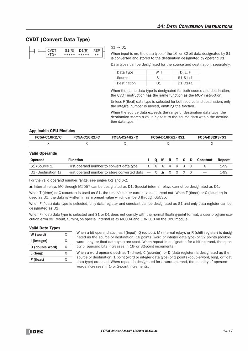
14: DATA CONVERSION INSTRUCTIONS
CVDT (Convert Data Type)
Applicable CPU Modules
Valid Operands
For the valid operand number range, see pages 6-1 and 6-2.
Internal relays M0 through M2557 can be designated as D1. Special internal relays cannot be designated as D1.
When T (timer) or C (counter) is used as S1, the timer/counter current value is read out. When T (timer) or C (counter) is used as D1, the data is written in as a preset value which can be 0 through 65535.
When F (float) data type is selected, only data register and constant can be designated as S1 and only data register can be designated as D1.
When F (float) data type is selected and S1 or D1 does not comply with the normal floating-point format, a user program exe-cution error will result, turning on special internal relay M8004 and ERR LED on the CPU module.
Valid Data Types
FC5A-C10R2/C FC5A-C16R2/C FC5A-C24R2/C FC5A-D16RK1/RS1 FC5A-D32K3/S3
X X X X X
Operand Function I Q M R T C D Constant Repeat
S1 (Source 1) First operand number to convert data type X X X X X X X X 1-99
D1 (Destination 1) First operand number to store converted data — X X X X X — 1-99
W (word) X
I (integer) X
D (double word) X
L (long) X
F (float) X
S1 → D1
When input is on, the data type of the 16- or 32-bit data designated by S1 is converted and stored to the destination designated by operand D1.
Data types can be designated for the source and destination, separately.
When the same data type is designated for both source and destination, the CVDT instruction has the same function as the MOV instruction.
Unless F (float) data type is selected for both source and destination, only the integral number is moved, omitting the fraction.
When the source data exceeds the range of destination data type, the destination stores a value closest to the source data within the destina-tion data type.
Data Type W, I D, L, FSource S1 S1·S1+1Destination D1 D1·D1+1
S1(R)*****
REP**
D1(R)*****
CVDT*TO*
When a bit operand such as I (input), Q (output), M (internal relay), or R (shift register) is desig-nated as the source or destination, 16 points (word or integer data type) or 32 points (double-word, long, or float data type) are used. When repeat is designated for a bit operand, the quan-tity of operand bits increases in 16- or 32-point increments.
When a word operand such as T (timer), C (counter), or D (data register) is designated as the source or destination, 1 point (word or integer data type) or 2 points (double-word, long, or float data type) are used. When repeat is designated for a word operand, the quantity of operand words increases in 1- or 2-point increments.
FC5A MICROSMART USER’S MANUAL 14-17

14: DATA CONVERSION INSTRUCTIONS
Examples: CVDT
• Data Type: Either S1 or D1 is not F (float)Unless F (float) data type is selected for both source and destination, only the integral number is moved, omitting the frac-tion.
• Data Type: S1 has a larger data range than D1When the source data exceeds the range of destination data type, the destination stores a value closest to the source data within the destination data type.
I0REPD1 –
D2SOTU
When input I0 is turned on, 3 is stored to data register D2.
Operand Data Type ValueSource F 3.141593Destination W 3
S1 –D0
CVDTFTOW
3D2
D1S1
3.141593D0·D1
I0REPD1 –
D2SOTU
When input I0 is turned on, 65535 is stored to data register D2.
Operand Data Type ValueSource D 4294967295Destination W 65535
S1 –D0
CVDTDTOW
65535D2
D1S1
4294967295D0·D1
14-18 FC5A MICROSMART USER’S MANUAL

15: WEEK PROGRAMMER INSTRUCTIONS
IntroductionWKTIM instructions can be used as many as required to turn on and off designated outputs and internal relays at predeter-mined times and days of the week.
Once the internal calendar/clock is set, the WKTIM instruction compares the predetermined time with the clock data in the clock cartridge. When the preset time is reached, internal relay or output designated as destination operand is turned on or off as scheduled. For setting the calendar/clock, see page 15-6.
For the specifications of the clock cartridge, see page 2-75.
WKTIM (Week Timer)
Applicable CPU Modules
Valid Operands
For the valid operand number range, see pages 6-1 and 6-2.
Internal relays M0 through M2557 can be designated as D1. Special internal relays cannot be designated as D1.
MODE — Week table output control (0 through 2)
0: Disable the week table
When the current day and time reach the presets for S1, S2, and S3, the designated output or internal relay is turned on or turned off. Set 0 for MODE when the WKTBL is not used; the WKTBL instruction is ignored even if it is pro-grammed.
1: Additional days in the week table
When the current time reaches the hour/minute comparison data set for S2 or S3 on the special day programmed in the WKTBL, the designated output or internal relay is turned on (S2) or turned off (S3).
2: Skip days in the week table
On the special day programmed in the WKTBL, the designated output or internal relay is not turned on or off, even when the current day and time reach the presets for S1, S2, and S3.
Note: When 1 or 2 is set for MODE, program special days in the week table using the WKTBL instruction, followed by the WKTIM instruction. If the WKTBL instruction is not programmed when 1 or 2 is set for MODE in the WKTIM instruc-tion, a user program execution error will result, turning on special internal relay M8004 and the ERR LED on the CPU module. The same error also occurs if the WKTIM instruction is executed before the WKTBL instruction.
FC5A-C10R2/C FC5A-C16R2/C FC5A-C24R2/C FC5A-D16RK1/RS1 FC5A-D32K3/S3
X X X X X
Operand Function I Q M R T C D Constant Repeat
MODE Week table output control — — — — — — — 0-2 —
S1 (Source 1) Day of week comparison data — — — — — — X 0-127 —
S2 (Source 2) Hour/minute comparison data to turn on — — — — — — X 0-2359 —
S3 (Source 3) Hour/minute comparison data to turn off — — — — — — X 0-2359 —
D1 (Destination 1) Comparison ON output — X — — — — — —
When input is on, the WKTIM compares the S1 and S2 preset data with the current day and time.
When the current day and time reach the presets, an output or internal relay designated by operand D1 is turned on, depend-ing on the week table output control designated by MODE.
WKTIMMODE
S1*****
S2*****
S3*****
D1*****
FC5A MICROSMART USER’S MANUAL 15-1

15: WEEK PROGRAMMER INSTRUCTIONS
S1 — Day of week comparison data (0 through 127)
Specify the days of week to turn on the output or internal relay designated by D1.
Designate the total of the values as operand S1 to turn on the output or internal relay.
Example: To turn on the output on Mondays through Fridays, designate 62 as S1 because 2 + 4 + 8 + 16 + 32 = 62.
S2 — Hour/minute comparison data to turn on S3 — Hour/minute comparison data to turn off
Specify the hours and minutes to turn on (S2) or to turn off (S3) the output or internal relay designated by D1.
Example: To turn on the output or internal relay at 8:30 a.m. using the WKTIM instruction, designate 830 as S2. To turn off the output or internal relay at 5:05 p.m., designate 1705 as S3.
When 10000 is set to hour/minute comparison data, the comparison data is ignored. For example, if 10000 is set to the hour/minute comparison data to turn off (S3), the WKTIM instruction compares only the hour/minute comparison data to turn on (S2).
When the hour/minute comparison data to turn on (S2) is larger than the hour/minute comparison data to turn off (S3), the comparison ON output (D1) turns on at S2 on the day designated by S1, remains on across 0 a.m., and turns off at S3 on the next day. For example, if S2 is 2300, S3 is 100, and Monday is included in S1, then the output designated by D1 turns on at 23 p.m. on Monday and turns off at 1 a.m. on Tuesday.
Make sure that the values set for MODE, S1, S2, and S3 are within the valid ranges. If any data is over the valid value, a user program execution error will result, turning on special internal relay M8004 and the ERR LED on the CPU module.
WKTBL (Week Table)
Applicable CPU Modules
Valid Operands
For the valid operand number range, see pages 6-1 and 6-2.
Day of Week Sunday Monday Tuesday Wednesday Thursday Friday Saturday
Value 1 2 4 8 16 32 64
Hour Minute Disable Comparison
00 through 23 00 through 59 10000
FC5A-C10R2/C FC5A-C16R2/C FC5A-C24R2/C FC5A-D16RK1/RS1 FC5A-D32K3/S3
X X X X X
Operand Function I Q M R T C D Constant Repeat
S1 (Source 1) Special month/day data — — — — — — X 101-1231 —
S1, S2, S3, ... , SN → Week Table (N ≤ 20)
When input is on, N blocks of special month/day data in oper-ands designated by S1, S2, S3, ... , SN are set to the week table.
The quantity of special days can be up to 20.
The special days stored in the week table are used to add or skip days to turn on or off the comparison outputs pro-grammed in subsequent WKTIM instructions.
The WKTBL must precede the WKTIM instructions.
WKTBL S1*****
S3*****
S2*****
..... SN
*****
15-2 FC5A MICROSMART USER’S MANUAL

15: WEEK PROGRAMMER INSTRUCTIONS
S1 through SN — Special month/day data
Specify the months and days to add or skip days to turn on or off the comparison outputs programmed in WKTIM instructions.
Example: To set July 4 as a special day, designate 704 as S1.
Make sure that the values set for S1 through SN are within the valid ranges. If any data is over the valid value, a user pro-gram execution error will result, turning on special internal relay M8004 and the ERR LED on the CPU module.
Examples: WKTIM and WKTBL
• Without Special Days (MODE = 0)This example is the basic program for week programmer application without using the WKTBL (week table) instruction. While the CPU is running, the WKTIM compares the S1, S2, and S3 preset data with the current day and time.
When the current day and time reach the presets, an output designated by operand D1 is turned on and off.
• With Additional Days in the Week Table (MODE = 1)When the current time reaches the hour/minute preset time on the special days programmed in the WKTBL, the designated output is turned on or turned off. In addition, the designated output is turned on and off every week as designated by oper-and S1 of WKTIM.
In normal execution, when the current day and time coincide with the preset day (S1) and time (S2 or S3) of the WKTIM, the designated output is turned on or off. Execution on the special days has precedence over execution on normal days.
This example demonstrates operation on special days in addition to regular weekends. The output is turned on from 10:30 a.m. to 11:10 p.m. on every Saturday and Sunday. Without regard to the day of week, the output is also turned on Decem-ber 31 through January 3.
• With Skip Days in the Week Table (MODE = 2)On the special days programmed in the WKTBL, the designated output is not turned on or off, while the designated output is turned on and off every week as designated by operand S1 of WKTIM.
In normal execution, when the current day and time coincide with the preset day (S1) and time (S2 or S3), the designated output is turned on or off. Execution on the special days has precedence over execution on normal days.
This example demonstrates operation aborted on special days. The output is turned on from 10:00 a.m. to 8:00 p.m. on every Monday through Friday, but is not turned on from May 2 through May 5.
Month Day
01 through 12 01 through 31
D1Q0
S162M8125
WKTIM0
S2830
S31715
M8125 is the in-operation output special internal relay.
S1 (62) specifies Monday through Friday.
The WKTIM turns on output Q0 at 8:30 and turns off output Q0 at 17:15 on Monday through Friday.
D1Q0
S165
WKTIM1
S21030
S32310
M8120 is the initialize pulse special internal relay.
WKTBL designates Dec. 31 to Jan. 3 as special days.
MODE (1) adds special days.
S1 (65) specifies Saturday and Sunday.
WKTIM turns on output Q0 at 10:30 and turns off at 23:10 on every Saturday, Sunday, and special days.
S4103
S11231M8120
S2101
S3102
WKTBL
M8125
D1Q0
S162
S21000
S32000
WKTBL designates May 2 to May 5 as special days.
MODE (2) skips special days.
S1 (62) specifies Monday to Friday.
WKTIM turns on output Q0 at 10:00 and turns off at 20:00 on every Monday through Friday except on special days.
S4505
S1502M8120
S2503
S3504
M8125
WKTBL
WKTIM2
FC5A MICROSMART USER’S MANUAL 15-3

15: WEEK PROGRAMMER INSTRUCTIONS
• Keep Output ON across 0 a.m.When the hour/minute comparison data to turn on (S2) is larger than the hour/minute comparison data to turn off (S3), the comparison ON output (D1) turns on at S2 on the day designated by S1, remains on across 0 a.m., and turns off at S3 on the next day. This example demonstrates a program to keep the designated output on across 0 a.m. and turn off the output on the next day.
• Keep Output ON for Several DaysMultiple WKTIM instructions can be used to keep an output on for more than 24 hours. This example demonstrates a pro-gram to keep the designated output on from 8 a.m on every Monday to 7 p.m. on every Friday.
D1Q0
S138M8125
WKTIM0
S22000
S3600
M8125 is the in-operation output special internal relay.
S1 (38) specifies Monday, Tuesday, and Friday.
The WKTIM turns on output Q0 at 20:00 on Monday, Tuesday, and Friday, and turns off output Q0 at 6:00 on the next day.
Sun Mon Tue Wed Thu Fri Sat
20:00 6:00
ONOutput Q0
20:00 6:00
ON
20:00 6:00
ON
D1M0
S12M8125
WKTIM0
S2800
S310000
M8125 is the in-operation output special internal relay.
S1 (2) specifies Monday.
S1 (28) specifies Tuesday, Wednesday, and Thursday.
S1 (32) specifies Friday.
S2 (10000) and S3 (10000) disable comparison of hour and minute data.
While internal relay M0, M1, or M2 is on, output Q0 remains on.
Sun Mon Tue Wed Thu Fri Sat
20:00 19:00
ONOutput Q0
D1M1
S128
WKTIM0
S210000
S310000
D1M2
S132
WKTIM0
S210000
S31900
M0
M1
M2
Q0
15-4 FC5A MICROSMART USER’S MANUAL
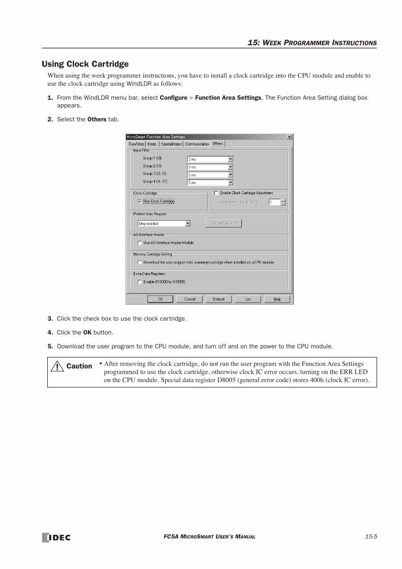
15: WEEK PROGRAMMER INSTRUCTIONS
Using Clock CartridgeWhen using the week programmer instructions, you have to install a clock cartridge into the CPU module and enable to use the clock cartridge using WindLDR as follows:
1. From the WindLDR menu bar, select Configure > Function Area Settings. The Function Area Setting dialog box appears.
2. Select the Others tab.
3. Click the check box to use the clock cartridge.
4. Click the OK button.
5. Download the user program to the CPU module, and turn off and on the power to the CPU module.
• After removing the clock cartridge, do not run the user program with the Function Area Settings programmed to use the clock cartridge, otherwise clock IC error occurs, turning on the ERR LED on the CPU module. Special data register D8005 (general error code) stores 400h (clock IC error).
Caution
FC5A MICROSMART USER’S MANUAL 15-5
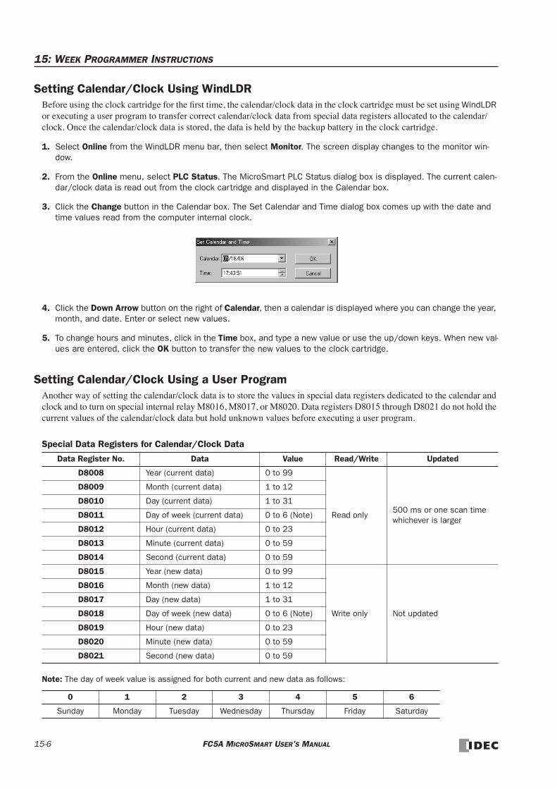
15: WEEK PROGRAMMER INSTRUCTIONS
Setting Calendar/Clock Using WindLDRBefore using the clock cartridge for the first time, the calendar/clock data in the clock cartridge must be set using WindLDR or executing a user program to transfer correct calendar/clock data from special data registers allocated to the calendar/clock. Once the calendar/clock data is stored, the data is held by the backup battery in the clock cartridge.
1. Select Online from the WindLDR menu bar, then select Monitor. The screen display changes to the monitor win-dow.
2. From the Online menu, select PLC Status. The MicroSmart PLC Status dialog box is displayed. The current calen-dar/clock data is read out from the clock cartridge and displayed in the Calendar box.
3. Click the Change button in the Calendar box. The Set Calendar and Time dialog box comes up with the date and time values read from the computer internal clock.
4. Click the Down Arrow button on the right of Calendar, then a calendar is displayed where you can change the year, month, and date. Enter or select new values.
5. To change hours and minutes, click in the Time box, and type a new value or use the up/down keys. When new val-ues are entered, click the OK button to transfer the new values to the clock cartridge.
Setting Calendar/Clock Using a User ProgramAnother way of setting the calendar/clock data is to store the values in special data registers dedicated to the calendar and clock and to turn on special internal relay M8016, M8017, or M8020. Data registers D8015 through D8021 do not hold the current values of the calendar/clock data but hold unknown values before executing a user program.
Special Data Registers for Calendar/Clock Data
Note: The day of week value is assigned for both current and new data as follows:
Data Register No. Data Value Read/Write Updated
D8008 Year (current data) 0 to 99
Read only500 ms or one scan time whichever is larger
D8009 Month (current data) 1 to 12
D8010 Day (current data) 1 to 31
D8011 Day of week (current data) 0 to 6 (Note)
D8012 Hour (current data) 0 to 23
D8013 Minute (current data) 0 to 59
D8014 Second (current data) 0 to 59
D8015 Year (new data) 0 to 99
Write only Not updated
D8016 Month (new data) 1 to 12
D8017 Day (new data) 1 to 31
D8018 Day of week (new data) 0 to 6 (Note)
D8019 Hour (new data) 0 to 23
D8020 Minute (new data) 0 to 59
D8021 Second (new data) 0 to 59
0 1 2 3 4 5 6
Sunday Monday Tuesday Wednesday Thursday Friday Saturday
15-6 FC5A MICROSMART USER’S MANUAL
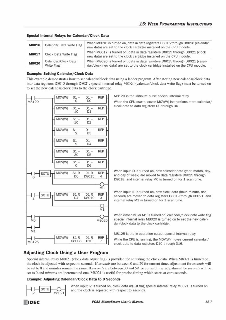
15: WEEK PROGRAMMER INSTRUCTIONS
Special Internal Relays for Calendar/Clock Data
Example: Setting Calendar/Clock DataThis example demonstrates how to set calendar/clock data using a ladder program. After storing new calendar/clock data into data registers D8015 through D8021, special internal relay M8020 (calendar/clock data write flag) must be turned on to set the new calendar/clock data to the clock cartridge.
Adjusting Clock Using a User ProgramSpecial internal relay M8021 (clock data adjust flag) is provided for adjusting the clock data. When M8021 is turned on, the clock is adjusted with respect to seconds. If seconds are between 0 and 29 for current time, adjustment for seconds will be set to 0 and minutes remain the same. If seconds are between 30 and 59 for current time, adjustment for seconds will be set to 0 and minutes are incremented one. M8021 is useful for precise timing which starts at zero seconds.
Example: Adjusting Calendar/Clock Data to 0 Seconds
M8016 Calendar Data Write FlagWhen M8016 is turned on, data in data registers D8015 through D8018 (calendar new data) are set to the clock cartridge installed on the CPU module.
M8017 Clock Data Write FlagWhen M8017 is turned on, data in data registers D8019 through D8021 (clock new data) are set to the clock cartridge installed on the CPU module.
M8020Calendar/Clock Data Write Flag
When M8020 is turned on, data in data registers D8015 through D8021 (calen-dar/clock new data) are set to the clock cartridge installed on the CPU module.
M8120
REP4
S1 RD0
MOV(W) D1 RD8015I0
SOTU
M8120 is the initialize pulse special internal relay.
When the CPU starts, seven MOV(W) instructions store calendar/clock data to data registers D0 through D6.
When input I0 is turned on, new calendar data (year, month, day, and day of week) are moved to data registers D8015 through D8018, and internal relay M0 is turned on for 1 scan time.
When input I1 is turned on, new clock data (hour, minute, and second) are moved to data registers D8019 through D8021, and internal relay M1 is turned on for 1 scan time.
When either M0 or M1 is turned on, calendar/clock data write flag special internal relay M8020 is turned on to set the new calen-dar/clock data to the clock cartridge.
M8125 is the in-operation output special internal relay.
While the CPU is running, the MOV(W) moves current calendar/clock data to data registers D10 through D16.
REP3
S1 RD4
MOV(W) D1 RD8019I1
SOTU
M0
M1
REP7
S1 RD8008
MOV(W) D1 RD10M8125
M1
M8020
REPS1 –0
MOV(W) D1 –D0
REPS1 –10
MOV(W) D1 –D1
REPS1 –10
MOV(W) D1 –D2
REPS1 –2
MOV(W) D1 –D3
REPS1 –9
MOV(W) D1 –D4
REPS1 –30
MOV(W) D1 –D5
REPS1 –0
MOV(W) D1 –D6
M0
I2SOTU
When input I2 is turned on, clock data adjust flag special internal relay M8021 is turned on and the clock is adjusted with respect to seconds.
M8021
FC5A MICROSMART USER’S MANUAL 15-7

15: WEEK PROGRAMMER INSTRUCTIONS
Adjusting Clock Cartridge AccuracyThe optional clock cartridge (FC4A-PT1) has an initial monthly error of ±2 minutes at 25°C. The accuracy of the clock cartridge can be improved to ±30 seconds using Enable Clock Cartridge Adjustment in the Function Area Settings.
Before starting the clock cartridge adjustment, confirm the adjustment value indicated on the clock cartridge. This value is an adjustment parameter measured on each clock cartridge at factory before shipment.
Programming WindLDR
1. From the WindLDR menu bar, select Configure > Function Area Settings. The Function Area Setting dialog box appears.
2. Select the Others tab.
3. Click the check box to enable the clock cartridge adjustment, and type the adjustment value found on the clock cartridge in the Adjustment Value field.
4. Click the OK button.
5. Download the user program to the CPU module, and turn off and on the power to the CPU module.
Clock Cartridge Backup DurationThe clock cartridge data is backed up by a lithium battery in the clock cartridge and held for approximately 30 days at 25°C. If the CPU module is not powered up for a period longer than the backup duration, the clock data is initialized to the following values.
Calendar: 00/01/01 Time: 0:00:00 AM
Adjustment Value
The adjustment value indicated on the clock cartridge was measured at 25°C to achieve the best accuracy. When using the clock cartridge at other temperatures, the clock cartridge accuracy may be impaired.
15-8 FC5A MICROSMART USER’S MANUAL

16: INTERFACE INSTRUCTIONS
IntroductionThe DISP (display) instruction is used to display 1 through 5 digits of timer/counter current values and data register data on 7-segment display units.
The DGRD (digital read) instruction is used to read 1 through 5 digits of digital switch settings to a data register. This instruction is useful to change preset values for timers and counters using digital switches.
DISP (Display)
Applicable CPU Modules
Note: The DISP instruction requires transistor output terminals. When using all-in-one 24-I/O type CPU module FC5A-C24R2, connect a transistor output module.
Valid Operands
For the valid operand number range, see pages 6-1 and 6-2.
Internal relays M0 through M2557 can be designated as Q. Special internal relays cannot be designated as Q. When T (timer) or C (counter) is used as S1, the timer/counter current value is read out.
ConversionBCD: To connect BCD (decimal) display units BIN: To connect BIN (hexadecimal) display units
Latch Phase and Data PhaseSelect the latch and data phases to match the phases of the display units in consideration of sink or source output of the output module.
Output PointsThe quantity of required output points is 4 plus the quantity of digits to display. When displaying 4 digits with output Q0 designated as the first output number, 8 consecutive output points must be reserved starting with Q0 through Q7.
Display Processing TimeDisplaying one digit of data requires 3 scan times after the input to the DISP instruction is turned on. Keep the input to the DISP instruction for the period of time shown below to process all digits of the display data.
When the scan time is less than 2 ms, the data cannot be displayed correctly. When the scan time is too short to ensure normal display, set a value of 3 or more (in ms) to data register D8022 (constant scan time preset value). See page 5-40.
FC5A-C10R2/C FC5A-C16R2/C FC5A-C24R2/C FC5A-D16RK1/RS1 FC5A-D32K3/S3
— — X X X
Operand Function I Q M R T C D Constant Repeat
S1 (Source 1) Data to display — — — — X X X — —
Q (Output) First output number to display data — X — — — — — —
Display Processing Time3 scan times × Quantity of digits
Latch phase:Low or High
Data phase:Low or High
Conversion:BCD or BIN
When input is on, data designated by source operand S1 is set to outputs or internal relays designated by operand Q. This instruction is used to output 7-segment data to display units.
Eight DISP instructions can be used in a user program.
Display data can be 0 through 65535 (FFFFh).
DISP DATS1*****
Q*****BCD4
LATLL
Quantity of digits:1 to 5 (decimal)1 to 4 (hex)
FC5A MICROSMART USER’S MANUAL 16-1

16: INTERFACE INSTRUCTIONS
Example: DISPThe following example demonstrates a program to display the 4-digit current value of counter CNT10 on 7-segment dis-play units (IDEC’s DD3S-F31N) connected to the transistor sink output module.
Output Wiring Diagram
When input I0 is on, the 4-digit current value of counter C10 is dis-played on 7-segment digital display units.I0
DATLATHL
S1C10
QQ30
DISPBCD4
(+)(–)
LatchABCD
(+)
(–)
24V DCPowerSupply
(+)(–)
LatchABCD
(+)(–)
LatchABCD
(+)(–)
LatchABCD
103 102 101 100
8-Transistor Sink
Upper Digit Lower Digit
FC4A-T08K1Output Module
Q30Q31Q32Q33Q34Q35Q36Q37
COM(–)+V
16-2 FC5A MICROSMART USER’S MANUAL

16: INTERFACE INSTRUCTIONS
DGRD (Digital Read)
Applicable CPU Modules
Note: The DGRD instruction requires transistor output terminals. When using all-in-one 24-I/O type CPU module FC5A-C24R2, connect a transistor output module.
Valid Operands
For the valid operand number range, see pages 6-1 and 6-2.
The DGRD instruction can read 65535 (5 digits) at the maximum. When the read value exceeds 65535 with the quantity of digits set to 5, a user program execution error will result, turning on special internal relay M8004 and the ERR LED on the CPU module.
Note: The DGRD instruction can be used up to 16 times in a user program. When transferring a user program containing more than 16 DGRD instructions to the CPU, a user program syntax error occurs, turning on the ERR LED. The user program cannot be executed.
ConversionBCD: To connect BCD (decimal) digital switches BIN: To connect BIN (hexadecimal) digital switches
Input PointsInputs are used to read the data from digital switches. The quantity of required input points is always 4. Four input points must be reserved starting with the input number designated by operand I. For example, when input I0 is designated as operand I, inputs I0 through I3 are used.
When using input terminals on the CPU module, the filter value has an effect (default value is 3 ms). Input terminals on expansion input modules have a fixed filter value of 4 ms. For Input Filter, see 5-37.
Output PointsOutputs are used to select the digits to read. The quantity of required output points is equal to the quantity of digits to read. When connecting the maximum of 5 digital switches, 5 output points must be reserved starting with the output number designated by operand Q. For example, when output Q0 is designated as operand Q to read 3 digits, outputs Q0 through Q2 are used.
Digital Switch Data Reading TimeReading digital switch data requires the following time after the input to the DGRD instruction is turned on. Keep the input to the DGRD instruction for the period of time shown below to read the digital switch data. For example, when read-ing data from 5 digital switches to the destination operand, 14 scans are required.
FC5A-C10R2/C FC5A-C16R2/C FC5A-C24R2/C FC5A-D16RK1/RS1 FC5A-D32K3/S3
— — X X X
Operand Function I Q M R T C D Constant Repeat
I First input number to read X — — — — — — — —
Q First output number for digit selection — X — — — — — — —
D1 (Destination 1) Destination to store results — — — — — — X — —
Digital Switch Data Reading Time2 scan times × (Quantity of digits + 2)
First input number
First output number
Conversion:BCD or BIN
Quantity of digits:1 to 5 (decimal)1 to 4 (hex)
When input is on, data designated by operands I and Q is set to a data register designated by destination operand D1.
This instruction can be used to change preset values for timer and counter instructions using digital switches. The data that can be read using this instruction is 0 through 65535 (5 dig-its), or FFFFh.
DGRD I*****
Q*****BCD4
D1*****
FC5A MICROSMART USER’S MANUAL 16-3

16: INTERFACE INSTRUCTIONS
Adjusting Scan TimeThe DGRD instruction requires a scan time longer than the filter time plus 6 ms.
The filter time depends on the input terminal used as shown below.
When the actual scan time is too short to execute the DGRD instruction, use the constant scan function. When the input fil-ter time is set to 3 ms, set a value of 9 or more (in ms) to special data register D8022 (constant scan time preset value). See page 5-40. When the input filter time is changed, set a proper value to D8022 to make sure of the minimum required scan time shown above.
Example: DGRDThe following example demonstrates a program to read data from four digital switches (IDEC’s DFBN-031D-B) to a data register in the CPU module, using a 8-point DC input module and a 16-point transistor sink output module.
I/O Wiring Diagram
Minimum Required Scan Time(Scan time) ≥ (Filter time) + 6 ms
Input Terminals Filter Time
I0 through I7 on CPU ModulesFilter value selected in the Function Area Settings (default 3 ms) See Input Filter on page 5-37.
I10 through I17 on CPU Modules 3 ms (fixed)
Inputs on Expansion Input Modules 4 ms (fixed)
When input I5 is on, the 4-digit value from BCD digital switches is read to data register D10.I5
II30
QQ30
D1D10
DGRDBCD4
Digital
1248
Switches
8-point DC Input ModuleFC4A-N08B1
16-point Transistor
FC4A-T16K3
103
102
101
100
Q30Q31Q32Q33Q34Q35Q36Q37
COM(–)+V
(+)
(–)
24V DCPowerSupply
I30I31I32I33I34I35I36I37
COMCOM
C
1248C
1248C
1248C
Sink Output Module
16-4 FC5A MICROSMART USER’S MANUAL

17: USER COMMUNICATION INSTRUCTIONS
IntroductionThis chapter describes the user communication function for communication between the MicroSmart and external devices with an RS232C or RS485 port, such as a computer, modem, printer, or barcode reader. The MicroSmart uses user com-munication instructions for transmitting and receiving communication to and from external devices.
User Communication OverviewEvery all-in-one CPU module has one RS232C port and port 2 connector as standard. By installing an optional RS232C communication adapter (FC4A-PC1) to the port 2 connector, the CPU module can communicate with two external devices simultaneously.
Every slim type CPU module has one RS232C port. An optional RS232C communication module can be attached to any slim type CPU module to use port 2 for additional RS232C communication. When an optional HMI base module is attached to a slim type CPU module, an optional RS232C communication adapter can be installed to the port 2 connector on the HMI base module.
When using an RS485 communication adapter or RS485 communication module for port 2, both all-in-one and slim type CPU modules can communicate with a maximum of 31 RS485 devices using the user communication.
User communication transmit and receive instructions can be programmed to match the communication protocol of the equipment to communicate with. Possibility of communication using the user communication mode can be determined referring to the user communication mode specifications described below.
User Communication Mode Specifications
Type RS232C User Communication RS485 User Communication
CPU Module and Communication Port
All CPU modules: Port 1 and Port 2 All CPU modules: Port 2
Connection Device Quantity 1 per port 31 maximum
Standards EIA RS232C EIA RS485
Baud Rate 1200, 2400, 4800, 9600, 19200, 38400, 57600 bps (Default: 9600)
Data Bits 7 or 8 bits (Default: 7)
Parity Odd, Even, None (Default: Even)
Stop Bits 1 or 2 bits (Default: 1)
Receive Timeout10 to 2540 ms (10-ms increments) or none (Receive timeout is disabled when 2550 ms is selected.)The receive timeout has an effect when using RXD instructions.
Communication Method Start-stop synchronization system half-duplex
Maximum Cable Length 2.4m 200m
Maximum Transmit Data 200 bytes
Maximum Receive Data 200 bytes
BCC CalculationXOR, ADD, ADD-2comp *, Modbus ASCII *, Modbus RTU * (* For calculation examples, see page 17-36.)
FC5A MICROSMART USER’S MANUAL 17-1

17: USER COMMUNICATION INSTRUCTIONS
Connecting RS232C Equipment through RS232C Port 1 or 2When using port 2 for RS232C communication on the all-in-one type CPU module, install the RS232C communication adapter (FC4A-PC1) to the port 2 connector.
When using port 2 for RS232C communication on the slim type CPU module, mount the RS232C communication module (FC4A-HPC1) to the left of the CPU module.
When using port 2 for RS232C communication on the slim type CPU module with the optional HMI module, install the RS232C communication adapter (FC4A-PC1) to the port 2 connector on the HMI base module.
To connect an RS232C communication device to the RS232C port 1 or 2 on the MicroSmart CPU module, use the user communication cable 1C (FC2A-KP1C). One end of the user communication cable 1C is not provided with a connector, and can be terminated with a proper connector to plug in to communicate with the RS232C port. See the figure on page 17-3.
17-2 FC5A MICROSMART USER’S MANUAL
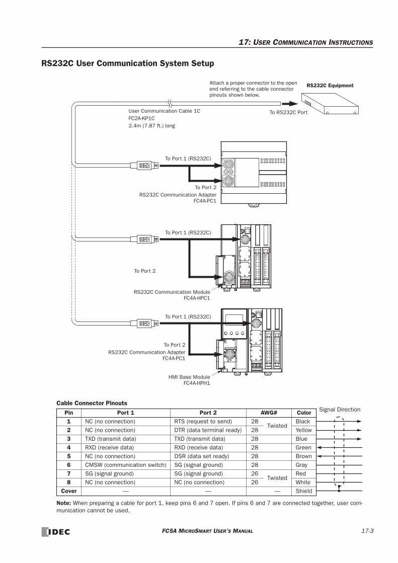
17: USER COMMUNICATION INSTRUCTIONS
RS232C User Communication System Setup
User Communication Cable 1CFC2A-KP1C2.4m (7.87 ft.) long
To RS232C Port
Attach a proper connector to the open end referring to the cable connector pinouts shown below.
Cable Connector Pinouts
Note: When preparing a cable for port 1, keep pins 6 and 7 open. If pins 6 and 7 are connected together, user com-munication cannot be used.
Pin Port 1 Port 2 AWG# Color1 NC (no connection) RTS (request to send) 28
TwistedBlack
2 NC (no connection) DTR (data terminal ready) 28 Yellow3 TXD (transmit data) TXD (transmit data) 28 Blue4 RXD (receive data) RXD (receive data) 28 Green5 NC (no connection) DSR (data set ready) 28 Brown6 CMSW (communication switch) SG (signal ground) 28 Gray7 SG (signal ground) SG (signal ground) 26
TwistedRed
8 NC (no connection) NC (no connection) 26 WhiteCover — — — Shield
RS232C Equipment
Signal Direction
To Port 2RS232C Communication Adapter
FC4A-PC1
To Port 1 (RS232C)
To Port 1 (RS232C)
To Port 2
RS232C Communication Module FC4A-HPC1
To Port 2RS232C Communication Adapter
FC4A-PC1
To Port 1 (RS232C)
HMI Base Module FC4A-HPH1
FC5A MICROSMART USER’S MANUAL 17-3

17: USER COMMUNICATION INSTRUCTIONS
Connecting RS485 Equipment through RS485 Port 2All MicroSmart CPU modules can use the RS485 user communication function. Using the RS485 user communication, a maximum of 31 RS485 devices can be connected to the MicroSmart CPU module.
When using port 2 for RS485 communication on the all-in-one type CPU module, install the RS485 communication adapter (FC4A-PC3) to the port 2 connector.
When using port 2 for RS485 communication on the slim type CPU module, mount the RS485 communication module (FC4A-HPC3) next to the CPU module.
When using port 2 for RS485 communication on the slim type CPU module with the optional HMI module, install the RS485 communication adapter (FC4A-PC3) to the port 2 connector on the HMI base module (FC4A-HPH1).
Connect RS485 device to the RS485 terminals A, B, and SG of port 2 on the MicroSmart CPU module using a shielded twisted pair cable as shown below. The total length of the cable for the RS485 user communication can be extended up to 200 meters (656 feet).
RS485 User Communication System Setup
31 devices maximum
RS485 Device
RS485 Device RS485 Device
Shielded twisted pair cable 200 meters (656 feet) maximumCore wire 0.3 mm2
Port 2RS485 Communication Adapter
FC4A-PC3
Port 2RS485 Communication Adapter
FC4A-PC3
HMI Base ModuleFC4A-HPH1
Port 2RS485 Communication Module
FC4A-HPC3
17-4 FC5A MICROSMART USER’S MANUAL

17: USER COMMUNICATION INSTRUCTIONS
Programming WindLDRWhen using the user communication function to communicate with an external RS232C or RS485 device, set the commu-nication parameters for the MicroSmart to match those of the external device.
Note: Since communication parameters in the Function Area Settings relate to the user program, the user program must be downloaded to the MicroSmart CPU module after changing any of these settings.
1. Select Configure from the WindLDR menu bar, then select Function Area Settings.
The Function Area Setting dialog box appears.
2. Click the Communication tab.
3. Select User Protocol in the Port 1 or Port 2 list box. (Click the Configure button when changing previous settings.)
The Communication Parameters dialog box appears.
When 2550 ms is selected in the Receive Timeout box, the receive timeout function is disabled.
4. Select communication parameters to the same values for the device to communicate with.
5. Click the OK button.
FC5A MICROSMART USER’S MANUAL 17-5

17: USER COMMUNICATION INSTRUCTIONS
TXD (Transmit)
Applicable CPU Modules
Valid Operands
For the valid operand number range, see pages 6-1 and 6-2.
Internal relays M0 through M2557 can be designated as D1. Special internal relays cannot be designated as D1.
Transmit data designated by operand S1 can be a maximum of 200 bytes.
When transmission is complete, an output or internal relay, designated by operand D1, is turned on.
Destination 2 occupies two consecutive data registers starting with the operand designated by D2. The transmit status data register, D0-D1998, D2000-D7998, or D10000-D49998, stores the status of transmission and error code. The next data register stores the byte count of transmitted data. The same data registers can not be used as transmit status registers for TXD1 and TXD2 instructions and receive status registers for RXD1 and RXD2 instructions.
The TXD instructions cannot be used in an interrupt program. If used, a user program execution error will result, turning on special internal relay M8004 and the ERR LED on the CPU module.
Precautions for Programming TXD Instruction• The MicroSmart has five formatting areas each for executing TXD1 and TXD2 instructions, so five instructions each of
TXD1 and TXD2 can be processed at the same time. If inputs to more than five of the same TXD instruction are turned on at the same time, an error code is set to the transmit status data register, designated by operand D2, in the excessive TXD instructions that cannot be executed.
• If the input for a TXD instruction is turned on while another TXD instruction is executed, the subsequent TXD instruction is executed 2 scan times after the preceding TXD instruction is completed.
• Since TXD instructions are executed in each scan while input is on, a pulse input from a SOTU or SOTD instruction should be used as required.
FC5A-C10R2/C FC5A-C16R2/C FC5A-C24R2/C FC5A-D16RK1/RS1 FC5A-D32K3/S3
X X X X X
Operand Function I Q M R T C D Constant Repeat
S1 (Source 1) Transmit data — — — — — — X X —
D1 (Destination 1) Transmit completion output — X — — — — — —
D2 (Destination 2) Transmit status register — — — — — — X — —
When input is on, data designated by S1 is converted into a specified format and transmitted from port 1 or port 2 to a remote terminal with an RS232C port.
TXD2 can be used to communicate with an RS485 remote terminal through port 2.
TXD*
S1*****
D1*****
D2*****
17-6 FC5A MICROSMART USER’S MANUAL
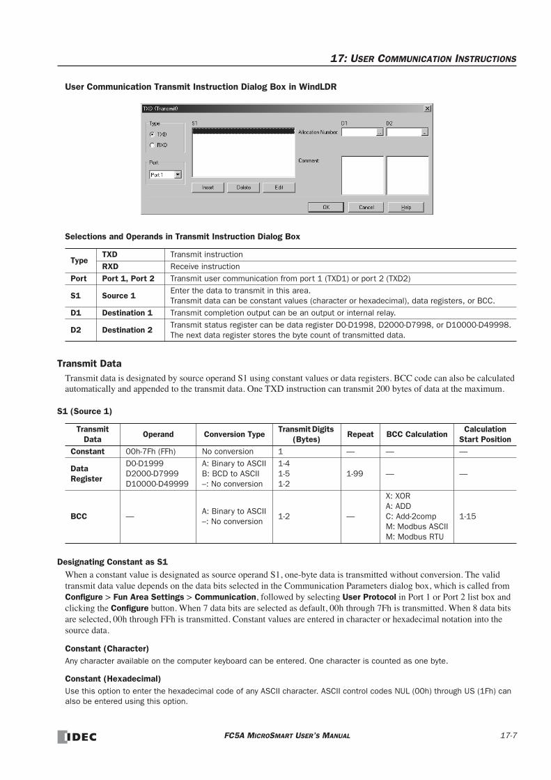
17: USER COMMUNICATION INSTRUCTIONS
User Communication Transmit Instruction Dialog Box in WindLDR
Selections and Operands in Transmit Instruction Dialog Box
Transmit DataTransmit data is designated by source operand S1 using constant values or data registers. BCC code can also be calculated automatically and appended to the transmit data. One TXD instruction can transmit 200 bytes of data at the maximum.
S1 (Source 1)
Designating Constant as S1When a constant value is designated as source operand S1, one-byte data is transmitted without conversion. The valid transmit data value depends on the data bits selected in the Communication Parameters dialog box, which is called from Configure > Fun Area Settings > Communication, followed by selecting User Protocol in Port 1 or Port 2 list box and clicking the Configure button. When 7 data bits are selected as default, 00h through 7Fh is transmitted. When 8 data bits are selected, 00h through FFh is transmitted. Constant values are entered in character or hexadecimal notation into the source data.
Constant (Character)Any character available on the computer keyboard can be entered. One character is counted as one byte.
Constant (Hexadecimal)Use this option to enter the hexadecimal code of any ASCII character. ASCII control codes NUL (00h) through US (1Fh) can also be entered using this option.
TypeTXD Transmit instructionRXD Receive instruction
Port Port 1, Port 2 Transmit user communication from port 1 (TXD1) or port 2 (TXD2)
S1 Source 1Enter the data to transmit in this area. Transmit data can be constant values (character or hexadecimal), data registers, or BCC.
D1 Destination 1 Transmit completion output can be an output or internal relay.
D2 Destination 2Transmit status register can be data register D0-D1998, D2000-D7998, or D10000-D49998. The next data register stores the byte count of transmitted data.
Transmit Data
Operand Conversion TypeTransmit Digits
(Bytes)Repeat BCC Calculation
Calculation Start Position
Constant 00h-7Fh (FFh) No conversion 1 — — —
Data Register
D0-D1999D2000-D7999D10000-D49999
A: Binary to ASCIIB: BCD to ASCII–: No conversion
1-41-51-2
1-99 — —
BCC —A: Binary to ASCII–: No conversion
1-2 —
X: XORA: ADDC: Add-2compM: Modbus ASCIIM: Modbus RTU
1-15
FC5A MICROSMART USER’S MANUAL 17-7
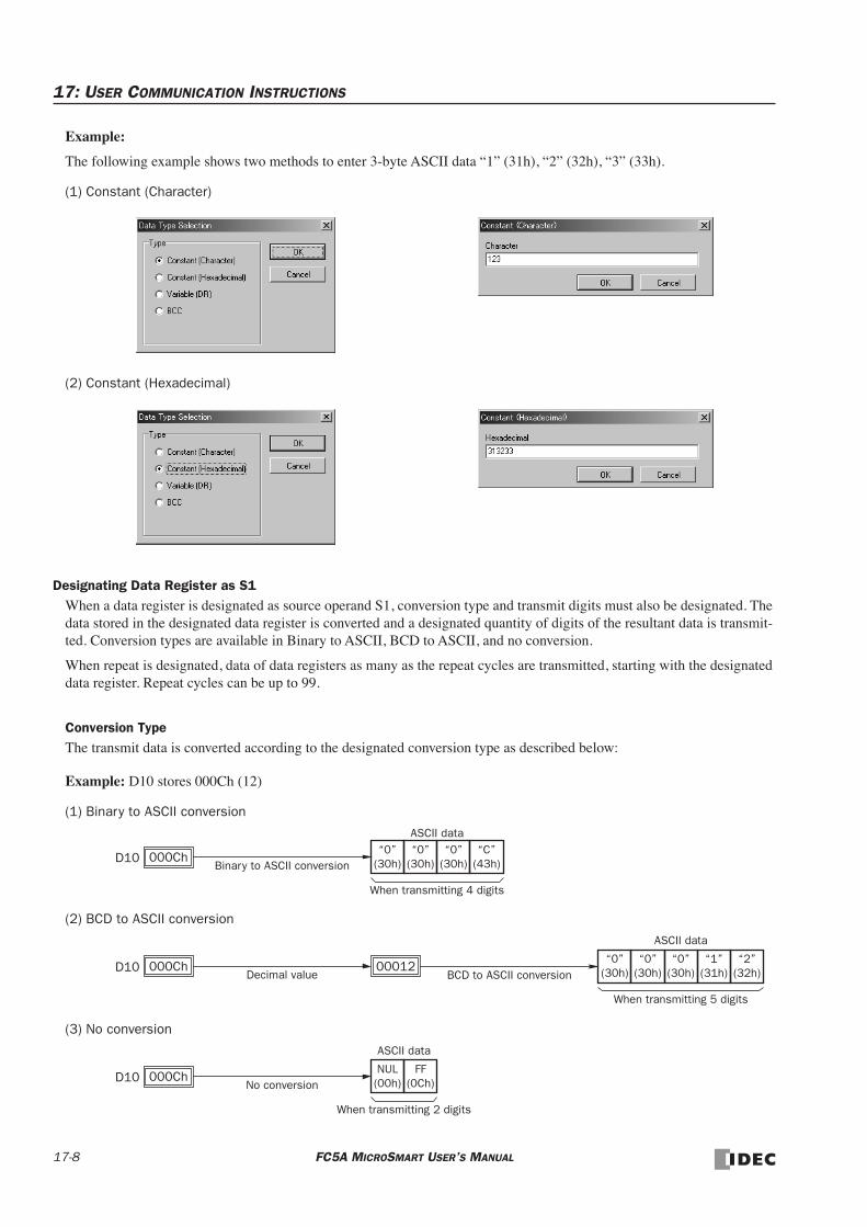
17: USER COMMUNICATION INSTRUCTIONS
Example:
The following example shows two methods to enter 3-byte ASCII data “1” (31h), “2” (32h), “3” (33h).
(1) Constant (Character)
(2) Constant (Hexadecimal)
Designating Data Register as S1When a data register is designated as source operand S1, conversion type and transmit digits must also be designated. The data stored in the designated data register is converted and a designated quantity of digits of the resultant data is transmit-ted. Conversion types are available in Binary to ASCII, BCD to ASCII, and no conversion.
When repeat is designated, data of data registers as many as the repeat cycles are transmitted, starting with the designated data register. Repeat cycles can be up to 99.
Conversion TypeThe transmit data is converted according to the designated conversion type as described below:
Example: D10 stores 000Ch (12)
(1) Binary to ASCII conversion
(2) BCD to ASCII conversion
(3) No conversion
000ChD10Binary to ASCII conversion
“0”(30h)
“0”(30h)
“0”(30h)
“C”(43h)
When transmitting 4 digits
ASCII data
000ChD10Decimal value
“0”(30h)
“0”(30h)
“0”(30h)
“1”(31h)
When transmitting 5 digits
00012BCD to ASCII conversion
“2”(32h)
ASCII data
000ChD10No conversion
NUL(00h)
FF(0Ch)
When transmitting 2 digits
ASCII data
17-8 FC5A MICROSMART USER’S MANUAL
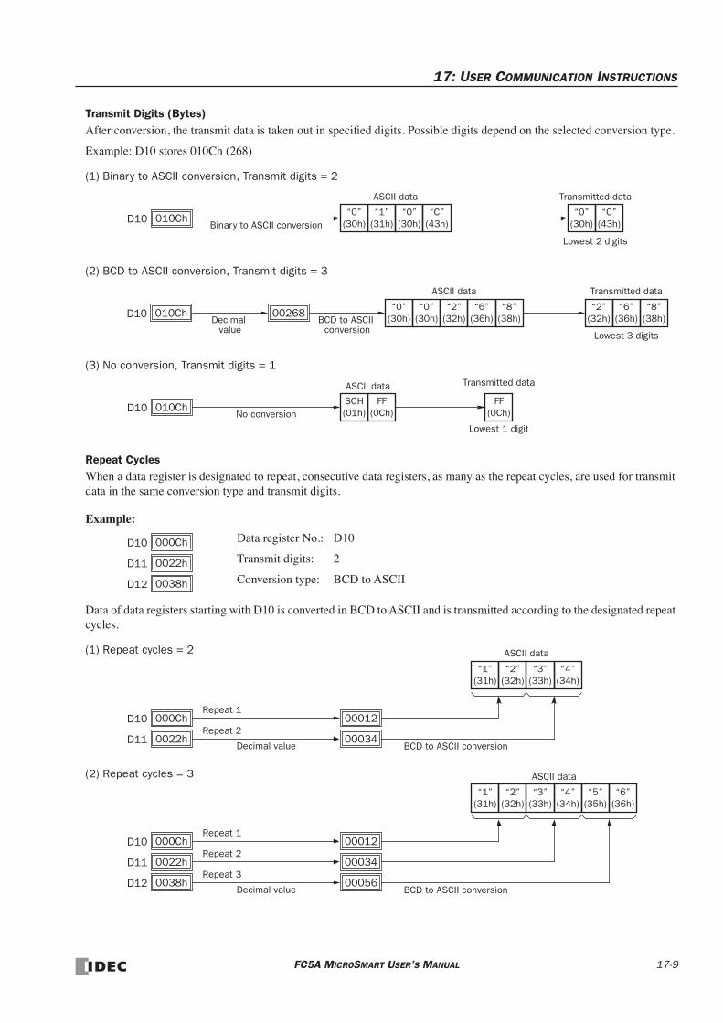
17: USER COMMUNICATION INSTRUCTIONS
Transmit Digits (Bytes)After conversion, the transmit data is taken out in specified digits. Possible digits depend on the selected conversion type.
Example: D10 stores 010Ch (268)
(1) Binary to ASCII conversion, Transmit digits = 2
(2) BCD to ASCII conversion, Transmit digits = 3
(3) No conversion, Transmit digits = 1
Repeat CyclesWhen a data register is designated to repeat, consecutive data registers, as many as the repeat cycles, are used for transmit data in the same conversion type and transmit digits.
Example:
Data of data registers starting with D10 is converted in BCD to ASCII and is transmitted according to the designated repeat cycles.
010ChD10Binary to ASCII conversion
“0”(30h)
“1”(31h)
“0”(30h)
“C”(43h)
Transmitted data
“0”(30h)
“C”(43h)
Lowest 2 digits
ASCII data
010ChD10Decimal
“0”(30h)
“0”(30h)
“2”(32h)
“6”(36h)
“8”(38h)
Lowest 3 digits
“2”(32h)
“6”(36h)
“8”(38h)BCD to ASCII
00268
value conversion
Transmitted dataASCII data
010ChD10No conversion
SOH(01h)
FF(0Ch)
FF(0Ch)
Lowest 1 digit
ASCII data Transmitted data
000ChD10
0022hD11
0038hD12
Data register No.: D10
Transmit digits: 2
Conversion type: BCD to ASCII
000ChD10
“1”(31h)
“2”(32h)
“3”(33h)
“4”(34h)
00012Repeat 1
0022hD11Decimal value
00034BCD to ASCII conversion
Repeat 2
ASCII data(1) Repeat cycles = 2
000ChD10
“1”(31h)
“2”(32h)
“3”(33h)
“4”(34h)
00012Repeat 1
0022hD11
Decimal value
00034
BCD to ASCII conversion
Repeat 2
0038hD12 00056Repeat 3
“5”(35h)
“6”(36h)
ASCII data(2) Repeat cycles = 3
FC5A MICROSMART USER’S MANUAL 17-9

17: USER COMMUNICATION INSTRUCTIONS
BCC (Block Check Character)Block check characters can be appended to the transmit data. The start position for the BCC calculation can be selected from the first byte through the 15th byte. The BCC can be 1 or 2 digits.
BCC Calculation Start PositionThe start position for the BCC calculation can be specified from the first byte through the 15th byte. The BCC is calculated for the range starting at the designated position up to the byte immediately before the BCC of the transmit data.
Example: Transmit data consists of 17 bytes plus 2 BCC digits.
(1) Calculation start position = 1
(2) Calculation start position = 2
BCC Calculation FormulaBCC calculation formula can be selected from XOR (exclusive OR), ADD (addition), ADD-2comp, Modbus ASCII, or Modbus RTU.
Example: Conversion results of transmit data consist of 41h, 42h, 43h, and 44h.
(1) BCC calculation formula = XOR
Calculation result = 41h ⊕ 42h ⊕ 43h ⊕ 44h = 04h
(2) BCC calculation formula = ADD
Calculation result = 41h + 42h + 43h + 44h = 10Ah → 0Ah (Only the last 1 or 2 digits are used as BCC.)
(3) BCC calculation formula = ADD-2comp
Calculation result = FEh, F6h (2 digits without conversion)
(4) BCC calculation formula = Modbus ASCII
Calculation result = 88 (ASCII)
(5) BCC calculation formula = Modbus RTU
Calculation result = 85h 0Fh (binary)
STX
BCC calculation start position can be selected from this range.
1st
“A”
2nd
“B”
3rd
“C”
4th
“D”
5th
“E”
6th
“0”
15th
CR
16th
LF
17th
BCC
18th
BCC
19th
BCC calculation range when starting with the 1st byte of the data.
BCC(2 digits)
STX
BCC calculation range
1st
“A”
2nd
“B”
3rd
“C”
4th
“D”
5th
“E”
6th
“0”
15th
CR
16th
LF
17th
BCC
18th
BCC
19th
BCC(2 digits)
STX
BCC calculation range
1st
“A”
2nd
“B”
3rd
“C”
4th
“D”
5th
“E”
6th
“0”
15th
CR
16th
LF
17th
BCC
18th
BCC
19th
BCC(2 digits)
“A”(41h)
“B”(42h)
“C”(43h)
“D”(44h)
ASCII data
17-10 FC5A MICROSMART USER’S MANUAL

17: USER COMMUNICATION INSTRUCTIONS
Conversion TypeThe BCC calculation result can be converted or not according to the designated conversion type as described below:
Example: BCC calculation result is 0041h.
(1) Binary to ASCII conversion
(2) No conversion
BCC Digits (Bytes)The quantity of digits (bytes) of the BCC code can be selected from 1 or 2.
Example:
Transmit Completion OutputDesignate an output, Q0 through Q627, or an internal relay, M0 through M2557, as an operand for the transmit completion output. Special internal relays cannot be used.
When the start input for a TXD instruction is turned on, preparation for transmission is initiated, followed by data trans-mission. When a sequence of all transmission operation is complete, the designated output or internal relay is turned on.
Transmit StatusDesignate a data register, D0-D1998, D2000-D7998, or D10000-D49998, as an operand to store the transmit status infor-mation including a transmission status code and a user communication error code.
Transmit Status Code
If the transmit status code is other than shown above, an error of transmit instruction is suspected. See User Communica-tion Error Code on page 17-27.
Transmit Status Code
Status Description
16 Preparing transmissionFrom turning on the start input for a TXD instruction, until the transmit data is stored in the internal transmit buffer
32 Transmitting dataFrom enabling data transmission by an END processing, until all data transmission is completed
48 Data transmission completeFrom completing all data transmission, until the END processing is completed for the TXD instruction
64 Transmit instruction completeAll transmission operation is completed and the next transmission is made possible
0041hBinary to ASCII conversion
“4”(34h)
“1”(31h)
2 digits
ASCII dataNote: On WindLDR, Modbus ASCII is defaulted to binary to ASCII conversion.
0041hNo conversion
NUL(00h)
“A”(41h)
2 digits
ASCII dataNote: On WindLDR, Modbus RTU is defaulted to no conversion.
(1) BCC digits = 2 “4”
(34h)“1”
(31h)“4”
(34h)“1”
(31h)
(2) BCC digits = 1 “4”
(34h)“1”
(31h)“1”
(31h) Lower digit
ASCII dataNote: On WindLDR, Modbus ASCII and Modbus RTU are defaulted to 2 digits.
FC5A MICROSMART USER’S MANUAL 17-11

17: USER COMMUNICATION INSTRUCTIONS
Transmit Data Byte CountThe data register next to the operand designated for transmit status stores the byte count of data transmitted by the TXD instruction. When BCC is included in the transmit data, the byte count of the BCC is also included in the transmit data byte count.
Example: Data register D100 is designated as an operand for transmit status.
Programming TXD Instruction Using WindLDRThe following example demonstrates how to program a TXD instruction including a start delimiter, BCC, and end delim-iter using WindLDR.
TXD sample program:
Data register contents:
Transmit data example:
1. Start to program a TXD instruction. Move the cursor where you want to insert the TXD instruction, and type TXD. You can also insert the TXD instruction by clicking the User Communication icon in the menu bar and clicking where you want to insert the TXD instruction in the program edit area.
The Transmit instruction dialog box appears.
D100 Transmit status
D101 Transmit data byte count
S112
D1M10I0
SOTU TXD1
D2D100
Communication port: Port 1
Transmit completion output: M10
Transmit status register: D100
Transmit data byte count: D101
04D2hD10
162EhD11
= 1234
= 5678
STX(02h)
D10
“1”(31h)
“2”(32h)
“3”(33h)
“4”(34h)
“5”(35h)
“8”(38h)
BCC
(41h)ETX
(03h)
BCC
“6”(36h)
“7”(37h)
BCC calculation range
Constant D11 Constant
(H)BCC
(36h)(L)
(hex) (hex)
17-12 FC5A MICROSMART USER’S MANUAL

17: USER COMMUNICATION INSTRUCTIONS
2. Check that TXD is selected in the Type box and select Port 1 in the Port box. Then, click Insert.
The Data Type Selection dialog box appears. You will program source operand S1 using this dialog box.
3. Click Constant (Hexadecimal) in the Type box and click OK. Next, in the Constant (Hexadecimal) dialog box, type 02 to program the start delimiter STX (02h). When finished, click OK.
4. Since the Transmit instruction dialog box reappears, repeat the above procedure. In the Data Type Selection dialog box, click Variable (DR) and click OK. Next, in the Variable (Data Register) dialog box, type D10 in the DR No. box and click BCD to ASCII to select the BCD to ASCII conversion. Enter 4 in the Digits box (4 digits) and 2 in the REP box (2 repeat cycles). When finished, click OK.
5. Again in the Data Type Selection dialog box, click BCC and click OK. Next, in the BCC dialog box, enter 1 in the Cal-culation Start Position box, select ADD for the Calculate Type, click BIN to ASCII for the Conversion Type, and click 2 for the Digits. When finished, click OK.
FC5A MICROSMART USER’S MANUAL 17-13

17: USER COMMUNICATION INSTRUCTIONS
6. Once again in the Data Type Selection dialog box, click Constant (Hexadecimal) and click OK. Next, in the Con-stant (Hexadecimal) dialog box, type 03 to program the end delimiter ETX (03h). When finished, click OK.
7. In the Transmit instruction dialog box, type M10 in the destination D1 box and type D100 in the destination D2 box. When finished, click OK.
Programming of the TXD1 instruction is complete and the transmit data is specified as follows:
STX(02h)
D10
“1”(31h)
“2”(32h)
“3”(33h)
“4”(34h)
“5”(35h)
“8”(38h)
BCC
(41h)ETX
(03h)
BCC
“6”(36h)
“7”(37h)
BCC calculation range
Constant D11 Constant
(H)BCC
(36h)(L)
(hex) (hex)
17-14 FC5A MICROSMART USER’S MANUAL

17: USER COMMUNICATION INSTRUCTIONS
RXD (Receive)
Applicable CPU Modules
Valid Operands
For the valid operand number range, see pages 6-1 and 6-2.
Internal relays M0 through M2557 can be designated as D1. Special internal relays cannot be designated as D1.
Receive format designated by operand S1 can be a maximum of 200 bytes.
When data receive is complete, an output or internal relay, designated by operand D1, is turned on.
Destination 2 occupies two consecutive data registers starting with the operand designated by D2. The receive status data register, D0-D1998, D2000-D7998, or D10000-D49998, stores the status of data receive and error code. The next data register stores the byte count of received data. The same data registers can not be used as transmit status registers for TXD1 and TXD2 instructions and receive status registers for RXD1 and RXD2 instructions.
While RXD1 or RXD2 instructions are ready for receiving data after a receive format is complete, turning on the user commu-nication receive instruction cancel flag M8022 or M8023 cancels all RXD1 and RXD2 instructions.
The RXD instructions cannot be used in an interrupt program. If used, a user program execution error will result, turning on special internal relay M8004 and the ERR LED on the CPU module.
Precautions for Programming the RXD Instruction• The MicroSmart can execute a maximum of five instructions each of RXD1 and RXD2 that have a start delimiter at the
same time. If a start delimiter is not programmed in RXD1 and RXD2 instructions, the MicroSmart can execute only one instruction each of RXD1 or RXD2 at a time. If the start input for a RXD1 or RXD2 instruction is turned on while another RXD1 or RXD2 instruction without a start delimiter is executed, a user communication error occurs.
• Since RXD instructions are executed in each scan while input is on, a pulse input from a SOTU or SOTD instruction should be used as required.
• Once the input to the RXD instruction is turned on, the RXD is activated and ready for receiving incoming communication even after the input is turned off. When the RXD completes data receiving, the RXD is deactivated if the input to the RXD is off. Or, if the input is on, the RXD is made ready for receiving another communication. Special internal relays are available to deactivate all RXD instructions waiting for incoming communication. For user communication receive instruction cancel flags, see page 17-24.
FC5A-C10R2/C FC5A-C16R2/C FC5A-C24R2/C FC5A-D16RK1/RS1 FC5A-D32K3/S3
X X X X X
Operand Function I Q M R T C D Constant Repeat
S1 (Source 1) Receive format — — — — — — X X —
D1 (Destination 1) Receive completion output — X — — — — — —
D2 (Destination 2) Receive status — — — — — — X — —
When input is on, data from an RS232C or RS485 remote terminal received by port 1 or port 2 is converted and stored in data registers according to the receive format designated by S1.
RXD2 can be used to communicate with an RS485 remote terminal through port 2.
S1*****
D1*****
D2*****
RXD*
FC5A MICROSMART USER’S MANUAL 17-15

17: USER COMMUNICATION INSTRUCTIONS
User Communication Receive Instruction Dialog Box in WindLDR
Selections and Operands in Receive Instruction Dialog Box
Receive FormatReceive format, designated by source operand S1, specifies data registers to store received data, data digits for storing data, data conversion type, and repeat cycles. A start delimiter and an end delimiter can be included in the receive format to discriminate valid incoming communication. When some characters in the received data are not needed, “skip” can be used to ignore a specified number of characters. BCC code can also be appended to the receive format to verify the received data. One RXD instruction can receive 200 bytes of data at the maximum.
S1 (Source 1)
Designating Data Register as S1When a data register is designated as source operand S1, receive digits and conversion type must also be designated. The received data is divided into a block of specified receive digits, converted in a specified conversion type, and stored to the designated data register. Conversion types are available in ASCII to Binary, ASCII to BCD, and no conversion.
When repeat is designated, received data is divided, converted, and stored into data registers as many as the repeat cycles, starting with the designated data register. Repeat cycles can be up to 99.
TypeTXD Transmit instructionRXD Receive instruction
Port Port 1, Port 2 Receive user communication to port 1 (RXD1) or port 2 (RXD2)
S1 Source 1Enter the receive format in this area.The receive format can include a start delimiter, data register to store incoming data, end delimiter, BCC, and skip.
D1 Destination 1 Receive completion output can be an output or internal relay.
D2 Destination 2Receive status register can be data register D0-D1998, D2000-D7998, or D10000-D49998.The next data register stores the byte count of received data.
Receive Format
OperandReceive Digits
(Bytes)Conversion Type Repeat BCC Calculation
Calculation Start
Position
Skip Bytes
Data Register
D0-D1999 D2000-D7999D10000-D49999
1-41-51-2
A: ASCII to BinaryB: ASCII to BCD–: No conversion
1-99 — — —
Start Delimiter
00h-7Fh (FFh) — No conversion — — — —
End Delimiter
00h-7Fh (FFh) — No conversion — — — —
BCC — 1-2A: Binary to ASCII–: No conversion
—
X: XORA: ADDC: Add-2compM: Modbus ASCIIM: Modbus RTU
1-15 —
Skip — — — — — — 1-99
17-16 FC5A MICROSMART USER’S MANUAL

17: USER COMMUNICATION INSTRUCTIONS
Receive DigitsThe received data is divided into a block of specified receive digits before conversion as described below:
Example: Received data of 6 bytes are divided in different receive digits. (Repeat is also designated.)
(1) Receive digits = 2 (2) Receive digits = 3
Conversion TypeThe data block of the specified receive digits is then converted according to the designated conversion type as described below:
Example: Received data has been divided into a 2-digit block.
(1) ASCII to Binary conversion
(2) ASCII to BCD conversion
(3) No conversion
Repeat CyclesWhen a data register is designated to repeat, the received data is divided and converted in the same way as specified, and the converted data is stored to consecutive data registers as many as the repeat cycles.
Example: Received data of 6 bytes is divided into 2-digit blocks, converted in ASCII to Binary, and stored to data registers starting at D20.
(1) Repeat cycles = 2
“1”(31h)
“2”(32h)
“3”(33h)
“4”(34h)
2 digits
“5”(35h)
“6”(36h)
2 digits 2 digits1st block 2nd block 3rd block
“1”(31h)
“2”(32h)
“3”(33h)
“4”(34h)
3 digits
“5”(35h)
“6”(36h)
3 digits1st block 2nd block
0012hASCII to Binary conversion
“1”(31h)
“2”(32h)
00012ASCII to BCD conversion
“1”(31h)
“2”(32h) 000Ch
Hexadecimal value
3132hNo conversion
“1”(31h)
“2”(32h)
0012hD20Repeat 1
0034hD21
ASCII to Binary conversion
Repeat 2
“1”(31h)
“2”(32h)
2 digits1st block
“3”(33h)
“4”(34h)
2 digits2nd block
FC5A MICROSMART USER’S MANUAL 17-17

17: USER COMMUNICATION INSTRUCTIONS
(2) Repeat cycles = 3
Designating Constant as Start DelimiterA start delimiter can be programmed at the first byte in the receive format of a RXD instruction; the MicroSmart will rec-ognize the beginning of valid communication, although a RXD instruction without a start delimiter can also be executed.
When a constant value is designated at the first byte of source operand S1, the one-byte data serves as a start delimiter to start the processing of the received data. The valid start delimiter value depends on the data bits selected in the Communi-cation Parameters dialog box, which is called from Configure > Fun Area Settings > Communication, followed by selecting User Protocol for Port 1 or Port 2 and clicking the Configure button. When 7 data bits are selected as default, start delimiters can be 00h through 7Fh. When 8 data bits are selected, start delimiters can be 00h through FFh. Constant values are entered in character or hexadecimal notation into the source data.
A maximum of five instructions each of RXD1 or RXD2 with different start delimiters can be executed at the same time. When the first byte of the incoming data matches the start delimiter of a RXD instruction, the received data is processed and stored according to the receive format specified in the RXD instruction. If the first byte of the incoming data does not match the start delimiter of any RXD instruction that is executed, the MicroSmart discards the incoming data and waits for the next communication.
While a RXD instruction without a start delimiter is executed, any incoming data is processed continuously according to the receive format. Only one instruction each of RXD1 or RXD2 without a start delimiter can be executed at a time. If start inputs to two or more RXD instructions without a start delimiter are turned on simultaneously, one at the smallest address is executed and the corresponding completion output is turned on.
Example:
(1) When a RXD instruction without a start delimiter is executed
0012hD20Repeat 1
0034hD21
ASCII to Binary conversion
Repeat 2
“1”(31h)
“2”(32h)
2 digits1st block
“3”(33h)
“4”(34h)
2 digits2nd block
“5”(35h)
“6”(36h)
2 digits3rd block
0056hD22Repeat 3
****hD100
When D100 is designated as the first data register
“0”(30h)
“1”(31h)
1stcharacter
“2”(32h)
“3”(33h)
Incoming Data
****hD100+n
****hD101
The incoming data is divided, converted, and stored to data registers according to the receive format.
17-18 FC5A MICROSMART USER’S MANUAL
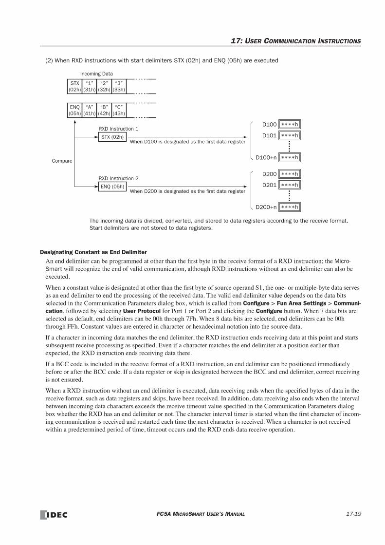
17: USER COMMUNICATION INSTRUCTIONS
(2) When RXD instructions with start delimiters STX (02h) and ENQ (05h) are executed
Designating Constant as End DelimiterAn end delimiter can be programmed at other than the first byte in the receive format of a RXD instruction; the Micro-Smart will recognize the end of valid communication, although RXD instructions without an end delimiter can also be executed.
When a constant value is designated at other than the first byte of source operand S1, the one- or multiple-byte data serves as an end delimiter to end the processing of the received data. The valid end delimiter value depends on the data bits selected in the Communication Parameters dialog box, which is called from Configure > Fun Area Settings > Communi-cation, followed by selecting User Protocol for Port 1 or Port 2 and clicking the Configure button. When 7 data bits are selected as default, end delimiters can be 00h through 7Fh. When 8 data bits are selected, end delimiters can be 00h through FFh. Constant values are entered in character or hexadecimal notation into the source data.
If a character in incoming data matches the end delimiter, the RXD instruction ends receiving data at this point and starts subsequent receive processing as specified. Even if a character matches the end delimiter at a position earlier than expected, the RXD instruction ends receiving data there.
If a BCC code is included in the receive format of a RXD instruction, an end delimiter can be positioned immediately before or after the BCC code. If a data register or skip is designated between the BCC and end delimiter, correct receiving is not ensured.
When a RXD instruction without an end delimiter is executed, data receiving ends when the specified bytes of data in the receive format, such as data registers and skips, have been received. In addition, data receiving also ends when the interval between incoming data characters exceeds the receive timeout value specified in the Communication Parameters dialog box whether the RXD has an end delimiter or not. The character interval timer is started when the first character of incom-ing communication is received and restarted each time the next character is received. When a character is not received within a predetermined period of time, timeout occurs and the RXD ends data receive operation.
****hD100RXD Instruction 1
STX(02h)
“1”(31h)
“2”(32h)
“3”(33h)
Incoming Data
****hD100+n
****hD101
The incoming data is divided, converted, and stored to data registers according to the receive format.Start delimiters are not stored to data registers.
ENQ(05h)
“A”(41h)
“B”(42h)
“C”(43h)
STX (02h)When D100 is designated as the first data register
****hD200RXD Instruction 2
****hD200+n
****hD201ENQ (05h)When D200 is designated as the first data register
Compare
FC5A MICROSMART USER’S MANUAL 17-19

17: USER COMMUNICATION INSTRUCTIONS
Example:
(1) When a RXD instruction without an end delimiter is executed
(2) When a RXD instruction with end delimiter ETX (03h) and without BCC is executed
(3) When a RXD instruction with end delimiter ETX (03h) and one-byte BCC is executed
SkipWhen “skip” is designated in the receive format, a specified quantity of digits in the incoming data are skipped and not stored to data registers. A maximum of 99 digits (bytes) of characters can be skipped continuously.
Example: When a RXD instruction with skip for 2 digits starting at the third byte is executed
****hD100When D100 is designated
“0”(30h)
“1”(31h)
Total of received characters
“2”(32h)
“3”(33h)
Incoming data
****hD100+n
****hD101
The incoming data is divided, converted, and stored to data registers according to the receive format. Receive operation is completed when the total characters programmed in RXD are received.
as the first data register
****hD100When D100 is designated
ETX(03h)
“1”(31h)
End delimiter
“2”(32h)
“3”(33h)
Incoming data
****hD100+n
****hD101
The incoming data is divided, converted, and stored to data registers according to the receive format. The end delimiter is not stored to a data register. Any data arriving after the end delimiter is discarded.
as the first data register
End of receiving data
****hD100When D100 is designated
ETX(03h)
“1”(31h)
End delimiter
“2”(32h)
BCCCode
Incoming data
****hD100+n
****hD101
The incoming data is divided, converted, and stored to data registers according to the receive format. The end delimiter and BCC code are not stored to data registers. After receiving the end delimiter, the MicroSmart receives only the one-byte BCC code.
as the first data register
End of receiving data
0035hD102
“1”(31h)
“2”(32h)
Skipped
“3”(33h)
“4”(34h)
Incoming Data
0038hD105
0036hD103
“5”(35h)
“6”(36h)
“7”(37h)
“8”(38h)
0031hD100
0032hD101
0037hD104
When D100 is designated as the first data register
17-20 FC5A MICROSMART USER’S MANUAL
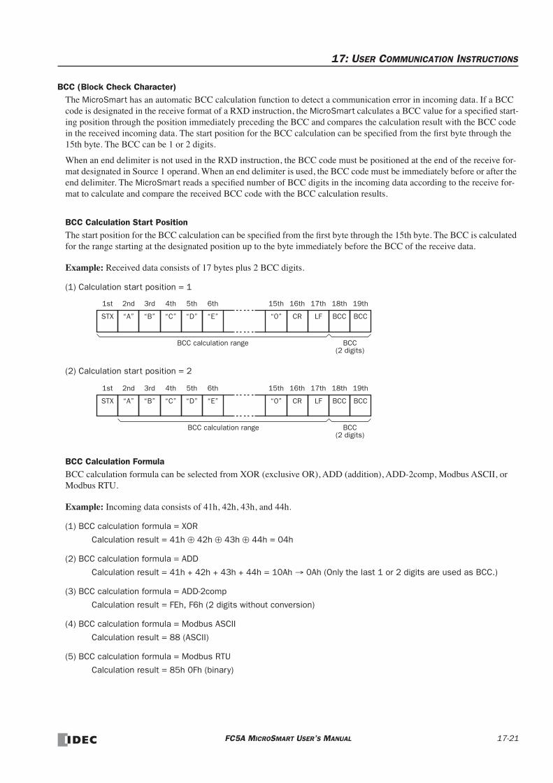
17: USER COMMUNICATION INSTRUCTIONS
BCC (Block Check Character)The MicroSmart has an automatic BCC calculation function to detect a communication error in incoming data. If a BCC code is designated in the receive format of a RXD instruction, the MicroSmart calculates a BCC value for a specified start-ing position through the position immediately preceding the BCC and compares the calculation result with the BCC code in the received incoming data. The start position for the BCC calculation can be specified from the first byte through the 15th byte. The BCC can be 1 or 2 digits.
When an end delimiter is not used in the RXD instruction, the BCC code must be positioned at the end of the receive for-mat designated in Source 1 operand. When an end delimiter is used, the BCC code must be immediately before or after the end delimiter. The MicroSmart reads a specified number of BCC digits in the incoming data according to the receive for-mat to calculate and compare the received BCC code with the BCC calculation results.
BCC Calculation Start PositionThe start position for the BCC calculation can be specified from the first byte through the 15th byte. The BCC is calculated for the range starting at the designated position up to the byte immediately before the BCC of the receive data.
Example: Received data consists of 17 bytes plus 2 BCC digits.
(1) Calculation start position = 1
(2) Calculation start position = 2
BCC Calculation FormulaBCC calculation formula can be selected from XOR (exclusive OR), ADD (addition), ADD-2comp, Modbus ASCII, or Modbus RTU.
Example: Incoming data consists of 41h, 42h, 43h, and 44h.
(1) BCC calculation formula = XOR
Calculation result = 41h ⊕ 42h ⊕ 43h ⊕ 44h = 04h
(2) BCC calculation formula = ADD
Calculation result = 41h + 42h + 43h + 44h = 10Ah → 0Ah (Only the last 1 or 2 digits are used as BCC.)
(3) BCC calculation formula = ADD-2comp
Calculation result = FEh, F6h (2 digits without conversion)
(4) BCC calculation formula = Modbus ASCII
Calculation result = 88 (ASCII)
(5) BCC calculation formula = Modbus RTU
Calculation result = 85h 0Fh (binary)
STX
BCC calculation range
1st
“A”
2nd
“B”
3rd
“C”
4th
“D”
5th
“E”
6th
“0”
15th
CR
16th
LF
17th
BCC
18th
BCC
19th
BCC(2 digits)
STX
BCC calculation range
1st
“A”
2nd
“B”
3rd
“C”
4th
“D”
5th
“E”
6th
“0”
15th
CR
16th
LF
17th
BCC
18th
BCC
19th
BCC(2 digits)
FC5A MICROSMART USER’S MANUAL 17-21

17: USER COMMUNICATION INSTRUCTIONS
Conversion TypeThe BCC calculation result can be converted or not according to the designated conversion type as described below:
Example: BCC calculation result is 0041h.
(1) Binary to ASCII conversion
(2) No conversion
BCC Digits (Bytes)The quantity of digits (bytes) of the BCC code can be selected from 1 or 2.
Example:
Comparing BCC CodesThe MicroSmart compares the BCC calculation result with the BCC code in the received incoming data to check for any error in the incoming communication due to external noises or other causes. If a disparity is found in the comparison, an error code is stored in the data register designated as receive status in the RXD instruction. For user communication error code, see page 17-27.
Example 1: BCC is calculated for the first byte through the sixth byte using the XOR format, converted in binary to ASCII, and compared with the BCC code appended to the seventh and eighth bytes of the incoming data.
0041hBinary to ASCII conversion
“4”(34h)
“1”(31h)
2 digits
Note: On WindLDR, Modbus ASCII is defaulted to binary to ASCII conversion.
0041hNo conversion
NUL(00h)
“A”(41h)
2 digits
Note: On WindLDR, Modbus RTU is defaulted to no conversion.
(1) BCC digits = 2 “4”
(34h)“1”
(31h)“4”
(34h)“1”
(31h)
(2) BCC digits = 1 “4”
(34h)“1”
(31h)“1”
(31h) Lower digit
Note: On WindLDR, Modbus ASCII and Modbus RTU are defaulted to 2 digits.
“1”(31h)
“2”(32h)
BCC Calculation Range
“3”(33h)
“4”(34h)
Incoming Data
“5”(35h)
“6”(36h)
“0”(30h)
“7”(37h)
BCC
31h ⊕ 32h ⊕ 33h ⊕ 34h ⊕ 35h ⊕ 36h = 07h
“0”(30h)
“7”(37h)
BCC Calculation Result
Binary to ASCII Conversion
Comparison result is true to indicate that data is received correctly.
17-22 FC5A MICROSMART USER’S MANUAL

17: USER COMMUNICATION INSTRUCTIONS
Example 2: BCC is calculated for the first byte through the sixth byte using the ADD format, converted in binary to ASCII, and compared with the BCC code appended to the seventh and eighth bytes of the incoming data.
Receive Completion OutputDesignate an output, Q0 through Q627, or internal relay, M0 through M2557, as an operand for the receive completion output.
When the start input for a RXD instruction is turned on, preparation for receiving data is initiated, followed by data con-version and storage. When a sequence of all data receive operation is complete, the designated output or internal relay is turned on.
Conditions for Completion of Receiving DataAfter starting to receive data, the RXD instruction can be completed in three ways:
• When an end delimiter is received (except when a BCC exists immediately after the end delimiter).
• When receive timeout occurs.
• When a specified byte count of data has been received.
Data receiving is completed when one of the above three conditions is met. To abort a RXD instruction, use the special inter-nal relay for user communication receive instruction cancel flag. See page 17-24.
Receive StatusDesignate a data register, D0-D1998, D2000-D7998, or D10000-D49998, as an operand to store the receive status infor-mation including a receive status code and a user communication error code.
Receive Status Code
If the receive status code is other than shown above, an error of receive instruction is suspected. See User Communication Error Code on page 17-27.
ReceiveStatus Code
Status Description
16 Preparing data receiveFrom turning on the start input for a RXD instruction to read the receive format, until the RXD instruction is enabled by an END processing
32 Receiving dataFrom enabling the RXD instruction by an END processing, until incom-ing data is received
48 Data receive completeFrom receiving incoming data, until the received data is converted and stored in data registers according to the receive format
64 Receive instruction completeAll data receive operation is completed and the next data receive is made possible
128User communication receive instruction cancel flag active
RXD instructions are cancelled by special internal relay for user com-munication receive instruction cancel flag, such as M8022 or M8023
“1”(31h)
“2”(32h)
BCC Calculation Range
“3”(33h)
“4”(34h)
Incoming Data
“5”(35h)
“6”(36h)
“0”(30h)
“7”(37h)
BCC
31h + 32h + 33h + 34h + 35h + 36h = 135h
“3”(33h)
“5”(35h)
BCC Calculation Result
Binary to ASCII Conversion
Comparison result is false.
Error code 9 is stored in the receive status data register.
FC5A MICROSMART USER’S MANUAL 17-23

17: USER COMMUNICATION INSTRUCTIONS
Receive Data Byte CountThe data register next to the operand designated for receive status stores the byte count of data received by the RXD instruction. When a start delimiter, end delimiter, and BCC are included in the received data, the byte counts for these codes are also included in the receive data byte count.
Example: Data register D200 is designated as an operand for receive status.
User Communication Receive Instruction Cancel Flag M8022/M8023Special internal relays M8022 and M8023 are used to cancel all RXD1 and RXD2 instructions, respectively. While the MicroSmart has completed receive format and is ready for receiving incoming data, turning on M8022 or M8023 cancels all receive instructions for port 1 or port 2, respectively. This function is useful to cancel receive instructions only, without stopping the MicroSmart.
To make the cancelled RXD instructions active, turn off the flag and turn on the input to the RXD instruction again.
Programming RXD Instruction Using WindLDRThe following example demonstrates how to program a RXD instruction including a start delimiter, skip, BCC, and end delimiter using WindLDR. Converted data is stored to data registers D20 and D21. Internal relay M20 is used as destination D1 for the receive completion output. Data register D200 is used as destination D2 for the receive status, and data register D201 is used to store the receive data byte count.
Receive data example:
RXD sample program:
1. Start to program a RXD instruction. Move the cursor where you want to insert the RXD instruction, and type RXD. You can also insert the RXD instruction by clicking the User Communication icon in the menu bar and clicking where you want to insert the RXD instruction in the program edit area, then the Transmit dialog box appears. Click RXD to change the dialog box to the Receive dialog box.
The Receive instruction dialog box appears.
D200 Receive status
D201 Receive data byte count
STX(02h)
Skip
“1”(31h)
“2”(32h)
“3”(33h)
“4”(34h)
“5”(35h)
“8”(38h)
BCC
(39h)ETX
(03h)
BCC
“6”(36h)
“7”(37h)
BCC calculation range
Start Stored to D20 End
(H)BCC
(32h)(L)
“9”(39h)
“B”(42h)
“0”(30h)
“A”(41h)
Stored to D21DelimiterDelimiter
S116
D1M20I0
SOTU RXD1
D2D200
Communication port: Port 1
Receive completion output: M20
Receive status register: D200
Receive data byte count: D201
17-24 FC5A MICROSMART USER’S MANUAL

17: USER COMMUNICATION INSTRUCTIONS
2. Check that RXD is selected in the Type box and select Port 1 in the Port box. Then, click Insert.
The Data Type Selection dialog box appears. You will program source operand S1 using this dialog box.
3. Click Constant (Hexadecimal) in the Type box and click OK. Next, in the Constant (Hexadecimal) dialog box, type 02 to program the start delimiter STX (02h). When finished, click OK.
4. Since the Receive instruction dialog box reappears, repeat the above procedure. In the Data Type Selection dialog box, click Skip and click OK. Next, in the Skip dialog box, type 4 in the Digits box and click OK.
5. Again in the Data Type Selection dialog box, click Variable (DR) and click OK. Next, in the Variable (Data Register) dialog box, type D20 in the DR No. box and click ASCII to BIN to select ASCII to binary conversion. Enter 4 in the Digits box (4 digits) and 2 in the REP box (2 repeat cycles). When finished, click OK.
FC5A MICROSMART USER’S MANUAL 17-25

17: USER COMMUNICATION INSTRUCTIONS
6. Again in the Data Type Selection dialog box, click BCC and click OK. Next, in the BCC dialog box, enter 1 in the Cal-culation Start Position box, select ADD for the Calculation Type, click BIN to ASCII for the Conversion Type, and click 2 for the Digits. When finished, click OK.
7. Once again in the Data Type Selection dialog box, click Constant (Hexadecimal) and click OK. Next, in the Con-stant (Hexadecimal) dialog box, type 03 to program the end delimiter ETX (03h). When finished, click OK.
8. In the Receive instruction dialog box, type M20 in the destination D1 box and type D200 in the destination D2 box. When finished, click OK.
Programming of the RXD1 instruction is complete and the receive data will be stored as follows:
5678hD20
90ABhD21
= 22136
= 37035
17-26 FC5A MICROSMART USER’S MANUAL

17: USER COMMUNICATION INSTRUCTIONS
User Communication ErrorWhen a user communication error occurs, a user communication error code is stored in the data register designated as a transmit status in the TXD instruction or as a receive status in the RXD instruction. When multiple errors occur, the final error code overwrites all preceding errors and is stored in the status data register.
The status data register also contains transmit/receive status code. To extract a user communication error code from the status data register, divide the value by 16. The remainder is the user communication error code. See pages 17-11 and 17-23.
To correct the error, correct the user program by referring to the error causes described below:
User Communication Error Code
User Communication
Error CodeError Cause Transmit/Receive Completion Output
1Start inputs to more than 5 TXD instructions are on simultaneously.
Transmit completion outputs of the first 5 TXD instructions from the top of the ladder diagram are turned on.
2 Transmission destination busy timeout Goes on after busy timeout.
3Start inputs to more than 5 RXD instructions with a start delimiter are on simultaneously.
Among the first 5 RXD instructions from the top of the ladder diagram, receive completion out-puts of RXD instructions go on if the start delim-iter matches the first byte of the received data.
4While a RXD instruction without a start delimiter is executed, another RXD instruction with or with-out a start delimiter is executed.
The receive completion output of the RXD instruc-tion at a smaller address goes on.
5 — Reserved — —6 — Reserved — —
7The first byte of received data does not match the specified start delimiter.
No effect on the receive completion output.If incoming data with a matching start delimiter is received subsequently, the receive completion output goes on.
8
When ASCII to binary or ASCII to BCD conversion is specified in the receive format, any code other than 0 to 9 and A to F is received. (These codes are regarded as 0 during conversion.)
The receive completion output goes on.
9BCC calculated from the RXD instruction does not match the BCC appended to the received data.
The receive completion output goes on.
10The end delimiter code specified in the RXD instruction does not match the received end delimiter code.
The receive completion output goes on.
11
Receive timeout between characters(After receiving one byte of data, the next byte is not received in the period specified for the receive timeout value.)
The receive completion output goes on.
12Overrun error(Before the receive processing is completed, the next data is received.)
The receive completion output goes off.
13Framing error(Detection error of start bit or stop bit)
No effect on the completion output.
14Parity check error(Error is found in the parity check.)
No effect on the completion output.
15TXD or RXD instruction is executed while user protocol is not selected for the communication port in the Function Area Settings.
No effect on the completion output.
FC5A MICROSMART USER’S MANUAL 17-27

17: USER COMMUNICATION INSTRUCTIONS
ASCII Character Code Table
Upper Bit
0 1 2 3 4 5 6 7 8 9 A B C D E FLower Bit
0 NULDLE SP 0 @ P ` p
Decimal 0 16 32 48 64 80 96 112 128 144 160 176 192 208 224 240
1 SOHDC1 ! 1 A Q a q
Decimal 1 17 33 49 65 81 97 113 129 145 161 177 193 209 225 241
2 STXDC2 ” 2 B R b r
Decimal 2 18 34 50 66 82 98 114 130 146 162 178 194 210 226 242
3 ETXDC3 # 3 C S c s
Decimal 3 19 35 51 67 83 99 115 131 147 163 179 195 211 227 243
4 EOTDC4 $ 4 D T d t
Decimal 4 20 36 52 68 84 100 116 132 148 164 180 196 212 228 244
5 ENQNAK % 5 E U e u
Decimal 5 21 37 53 69 85 101 117 133 149 165 181 197 213 229 245
6 ACKSYN & 6 F V f v
Decimal 6 22 38 54 70 86 102 118 134 150 166 182 198 214 230 246
7 BELETB ’ 7 G W g w
Decimal 7 23 39 55 71 87 103 119 135 151 167 183 199 215 231 247
8 BS CAN ( 8 H X h x
Decimal 8 24 40 56 72 88 104 120 136 152 168 184 200 216 232 248
9 HT EM ) 9 I Y i y
Decimal 9 25 41 57 73 89 105 121 137 153 169 185 201 217 233 249
A LF SUB * : J Z j z
Decimal 10 26 42 58 74 90 106 122 138 154 170 186 202 218 234 250
B VT ESC + ; K [ k
Decimal 11 27 43 59 75 91 107 123 139 155 171 187 203 219 235 251
C FF FS , < L \ l |
Decimal 12 28 44 60 76 92 108 124 140 156 172 188 204 220 236 252
D CR GS - = M ] m
Decimal 13 29 45 61 77 93 109 125 141 157 173 189 205 221 237 253
E SO RS . > N ^ n ~
Decimal 14 30 46 62 78 94 110 126 142 158 174 190 206 222 238 254
F SI US / ? O _ o
Decimal 15 31 47 63 79 95 111 127 143 159 175 191 207 223 239 255
17-28 FC5A MICROSMART USER’S MANUAL

17: USER COMMUNICATION INSTRUCTIONS
RS232C Line Control SignalsWhile the MicroSmart is in the user communication mode, special data registers can be used to enable or disable DSR and DTR control signal options for port 2. The DSR and DTR control signal options cannot be used for port 1.
The RTS signal line of port 2 remains on.
Special Data Registers for Port 2 RS232C Line Control SignalsSpecial data registers D8104 through D8106 and D8204 through D8206 are allocated for RS232C line control signals.
Control Signal Status D8104Special data register D8104 stores a value to show that DSR and DTR are on or off at port 2. The data of D8104 is updated at every END processing.
DSR Control Signal Status in RUN and STOP Modes
DTR Control Signal Status in RUN and STOP Modes
RS232C Port DR No. Data Register Function DR Value Updated R/W
Port 2
D8104 Control signal status Every scan R
D8105 DSR input control signal option When sending/receiving data R/W
D8106 DTR output control signal option When sending/receiving data R/W
D8104 Value DSR DTR Description
0 OFF OFF Both DSR and DTR are off
1 OFF ON DTR is on
2 ON OFF DSR is on
3 ON ON Both DSR and DTR are on
CommunicationMode
D8105/D8205 ValueDSR (Input) Status
RUN Mode STOP Mode
User Communication Mode
0 (default) No effect No effect (TXD/RXD disabled)
1ON: Enable TXD/RXD OFF: Disable TXD/RXD
No effect (TXD/RXD disabled)
2ON: Disable TXD/RXD OFF: Enable TXD/RXD
No effect (TXD/RXD disabled)
3ON: Enable TXD OFF: Disable TXD
No effect (TXD/RXD disabled)
4ON: Disable TXD OFF: Enable TXD
No effect (TXD/RXD disabled)
5 or more No effect No effect (TXD/RXD disabled)Maintenance Mode — No effect No effect
CommunicationMode
D8106/D8206 ValueDTR (Output) Status
RUN Mode STOP Mode
User Communication Mode
0 (default) ON OFF1 OFF OFF
2RXD enabled: ON RXD disabled: OFF
OFF
3 or more ON OFFMaintenance Mode — ON ON
FC5A MICROSMART USER’S MANUAL 17-29
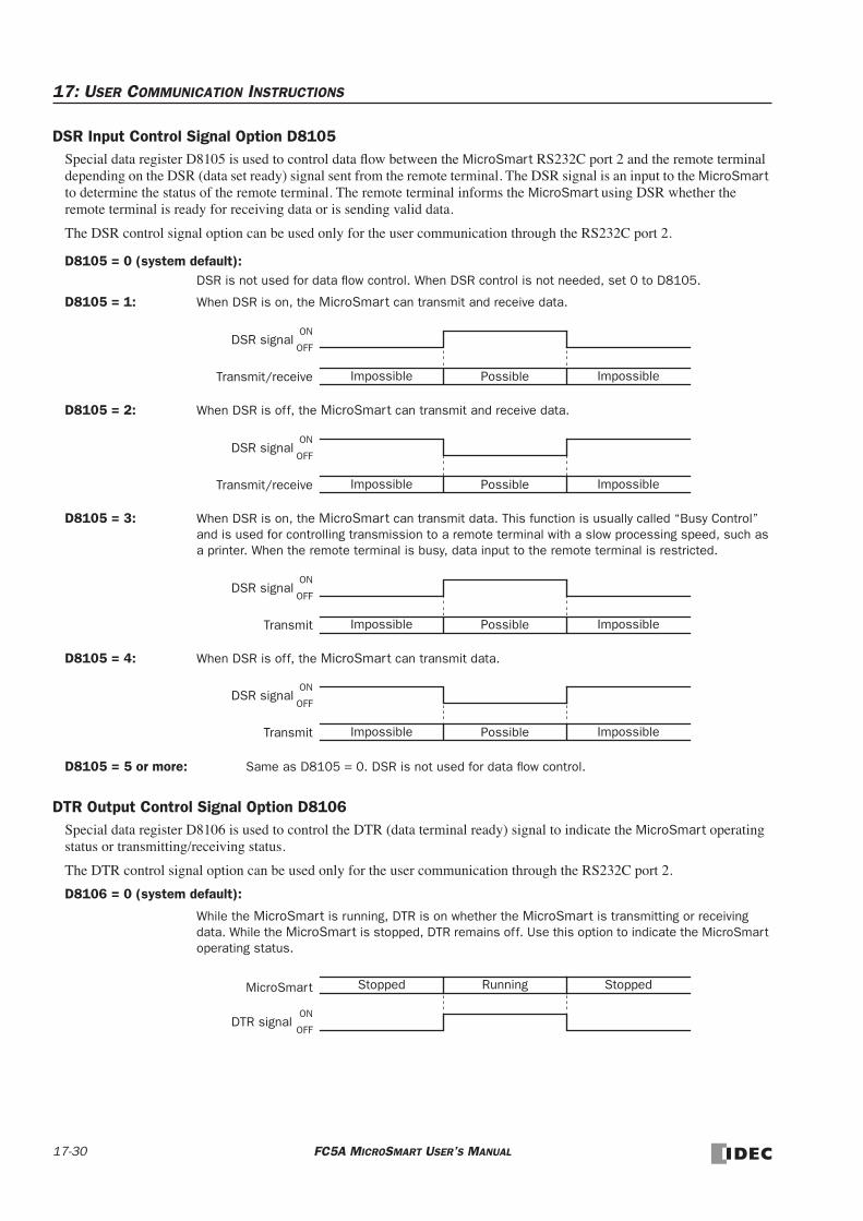
17: USER COMMUNICATION INSTRUCTIONS
DSR Input Control Signal Option D8105Special data register D8105 is used to control data flow between the MicroSmart RS232C port 2 and the remote terminal depending on the DSR (data set ready) signal sent from the remote terminal. The DSR signal is an input to the MicroSmart to determine the status of the remote terminal. The remote terminal informs the MicroSmart using DSR whether the remote terminal is ready for receiving data or is sending valid data.
The DSR control signal option can be used only for the user communication through the RS232C port 2.
D8105 = 0 (system default):DSR is not used for data flow control. When DSR control is not needed, set 0 to D8105.
D8105 = 1: When DSR is on, the MicroSmart can transmit and receive data.
D8105 = 2: When DSR is off, the MicroSmart can transmit and receive data.
D8105 = 3: When DSR is on, the MicroSmart can transmit data. This function is usually called “Busy Control” and is used for controlling transmission to a remote terminal with a slow processing speed, such as a printer. When the remote terminal is busy, data input to the remote terminal is restricted.
D8105 = 4: When DSR is off, the MicroSmart can transmit data.
D8105 = 5 or more: Same as D8105 = 0. DSR is not used for data flow control.
DTR Output Control Signal Option D8106Special data register D8106 is used to control the DTR (data terminal ready) signal to indicate the MicroSmart operating status or transmitting/receiving status.
The DTR control signal option can be used only for the user communication through the RS232C port 2.
D8106 = 0 (system default):
While the MicroSmart is running, DTR is on whether the MicroSmart is transmitting or receiving data. While the MicroSmart is stopped, DTR remains off. Use this option to indicate the MicroSmart operating status.
DSR signalON
OFF
PossibleImpossible ImpossibleTransmit/receive
DSR signalON
OFF
PossibleImpossible ImpossibleTransmit/receive
DSR signalON
OFF
PossibleImpossible ImpossibleTransmit
DSR signalON
OFF
PossibleImpossible ImpossibleTransmit
MicroSmart
DTR signalON
OFF
Stopped Running Stopped
17-30 FC5A MICROSMART USER’S MANUAL

17: USER COMMUNICATION INSTRUCTIONS
D8106 = 1: Whether the MicroSmart is running or stopped, DTR remains off.
D8106 = 2: While the MicroSmart can receive data, DTR is turned on. While the MicroSmart can not receive data, DTR remains off. Use this option when flow control of receive data is required.
D8106 = 3 or more: Same as D8106 = 0.
MicroSmart
DTR signalON
OFF
Stopped Running Stopped
DTR signalON
OFF
PossibleImpossible ImpossibleReceive
FC5A MICROSMART USER’S MANUAL 17-31

17: USER COMMUNICATION INSTRUCTIONS
Sample Program – User Communication TXDThis example demonstrates a program to send data to a printer using the user communication TXD2 (transmit) instruction, with the optional RS232C communication adapter installed on the port 2 connector of the 24-I/O type CPU module.
System Setup
The name of BUSY terminal differs depending on printers, such as DTR. The function of this terminal is to send a signal to remote equipment whether the printer is ready to print data or not. Since the operation of this signal may differ depend-ing on printers, confirm the operation before connecting the cable.
Description of OperationThe data of counter C2 and data register D30 are printed every minute. A printout example is shown on the right.
Programming Special Data RegisterSpecial data register D8105 is used to monitor the BUSY signal and to control the transmission of print data.
The MicroSmart monitors the DSR signal to prevent the receive buffer of the printer from overflowing. For the DSR sig-nal, see page 17-30.
Special DR Value Description
D8105 3
While DSR is on (not busy), the CPU sends data.While DSR is off (busy), the CPU stops data transmission.If the off duration exceeds a limit (approx. 5 sec), a trans-mission busy timeout error will occur, and the remaining data is not sent. The transmit status data register stores an error code. See pages 17-11 and 17-27.
To RS232C Port
D-sub 9-pin Connector Pinouts
Pin Description1 NC No Connection2 NC No Connection3 DATA Receive Data4 NC No Connection5 GND Ground6 NC No Connection7 NC No Connection8 BUSY Busy Signal9 NC No Connection
Printer
Mini DIN Connector Pinouts
Description Color PinShield — CoverNC No Connection Black 1NC No Connection Yellow 2TXD Transmit Data Blue 3NC No Connection Green 4DSR Data Set Ready Brown 5NC No Connection Gray 6SG Signal Ground Red 7NC No Connection White 8
User Communication Cable 1CFC2A-KP1C 2.4m (7.87 ft.) long
Attach a proper connector to the open end of the cable referring to the cable connec-tor pinouts shown below.
Cable Connection and Pinouts
To Port 2 (RS232C)
RS232C Communication AdapterFC4A-PC1
Caution • Do not connect any wiring to the NC (no connection) pins; otherwise, the MicroSmart and the printer may not work correctly and may be damaged.
--- PRINT TEST ---
11H 00M
CNT2...0050D030...3854
--- PRINT TEST ---
11H 01M
CNT2...0110D030...2124
Printout Example
17-32 FC5A MICROSMART USER’S MANUAL

17: USER COMMUNICATION INSTRUCTIONS
Setting User Communication Mode in WindLDR Function Area SettingsSince this example uses the RS232C port 2, select User Protocol for Port 2 in the Function Area Settings using WindLDR. See page 17-5.
Setting Communication ParametersSet the communication parameters to match those of the printer. See page 17-5. For details of the communication parame-ters of the printer, see the user’s manual for the printer. An example is shown below:
Note: The receive timeout value is used for the RXD instruction in the user communication mode. Since this example uses only the TXD instruction, the receive timeout value has no effect.
Ladder DiagramThe second data stored in special data register D8014 is compared with 0 using the CMP= (compare equal to) instruction. Each time the condition is met, the TXD2 instruction is executed to send the C2 and D30 data to the printer. A counting circuit for counter C2 is omitted from this sample program.
Communication Parameters:Baud rate 9600 bpsData bits 8Parity check NoneStop bits 1
S1 –3M8120
REPD1 –D8105
S2 –0
REPD1 –M0
M8120 is the initialize pulse special internal relay.
3 → D8105 to enable the DSR option for busy control.
M8125 is the in-operation output special internal relay.
CMP=(W) compares the D8014 second data with 0.
When the D8014 data equals 0 second, M0 is turned on.
Counter C2 current value is moved to D31.
D8012 hour data is moved to D20.
D8013 minute data is moved to D21.
TXD2 is executed to send 73-byte data through the RS232C port 2 to the printer.
D20 hour data is converted from BCD to ASCII, and 2 digits are sent.
D21 minute data is converted from BCD to ASCII, and 2 dig-its are sent.
D31 counter C2 data is converted from BCD to ASCII, and 4 digits are sent.
D30 data is converted from BCD to ASCII, and 4 digits are sent.
END
SOTU
SP20h
SP20h
SP20h
–2Dh
–2Dh
–2Dh
SP20h
P50h
R52h
I49h
N4Eh
T54h
SP20h
T54h
E45h
S53h
T54h
SP20h
–2Dh
–2Dh
–2Dh
CR0Dh
LF0Ah
CR0Dh
LF0Ah
SP20h
SP20h
SP20h
D20 Conversion: BCD→ASCII Digits: 2 REP: 01
H48h
SP20h
D21 Conversion: BCD→ASCII Digits: 2 REP: 01
M4Dh
CR0Dh
LF0Ah
CR0Dh
LF0Ah
SP20h
SP20h
SP20h
C43h
N4Eh
T54h
232h
.2Eh
.2Eh
.2Eh
D31 Conversion: BCD→ASCII Digits: 4 REP: 01
CR0Dh
LF0Ah
SP20h
SP20h
SP20h
D44h
030h
333h
030h
.2Eh
.2Eh
.2Eh
D30 Conversion: BCD→ASCII Digits: 4 REP: 01
CR0Dh
LF0Ah
CR0Dh
LF0Ah
S173
D2D0
D1M1
M0
M0
MOV(W)
TXD2
CMP=(W) S1 –D8014M8125
S1 –C2
REPD1 –D31
MOV(W)
S1 –D8012
REPD1 –D20
MOV(W)
S1 –D8013
REPD1 –D21
MOV(W)
FC5A MICROSMART USER’S MANUAL 17-33

17: USER COMMUNICATION INSTRUCTIONS
Sample Program – User Communication RXDThis example demonstrates a program to receive data from a barcode reader with a RS232C port using the user communi-cation RXD1 (receive) instruction.
System Setup
Description of OperationA barcode reader is used to scan barcodes of 8 numerical digits. The scanned data is sent to the MicroSmart through the RS232C port 1 and stored to data registers. The upper 8 digits of the data are stored to data register D20 and the lower 8 digits are stored to data register D21.
Setting User Communication Mode in WindLDR Function Area SettingsSince this example uses the RS232C port 1, select User Protocol for Port 1 in the Function Area Settings using WindLDR. See page 17-5.
Setting Communication ParametersSet the communication parameters to match those of the barcode reader. See page 17-5. For details of the communication parameters of the barcode reader, see the user’s manual for the barcode reader. An example is shown below:
Communication Parameters:Baud rate 9600 bpsData bits 7Parity check EvenStop bits 1
To RS232C Port
D-sub 25-pin Connector Pinouts
Pin Description1 FG Frame Ground2 TXD1 Transmit Data3 RXD1 Receive Data7 GND Ground
Barcode Reader
Mini DIN Connector Pinouts
Description Color PinShield — CoverNC No Connection Black 1NC No Connection Yellow 2TXD Transmit Data Blue 3RXD Receive Data Green 4NC No Connection Brown 5NC No Connection Gray 6SG Signal Ground Red 7NC No Connection White 8
To RS232C Port 1
User Communication Cable 1CFC2A-KP1C 2.4m (7.87 ft.) long
Attach a proper connector to the open end of the cable referring to the cable connec-tor pinouts shown below.
IDEC DATALOGICDS4600A
Caution • Do not connect any wiring to the NC (no connection) pins; otherwise, the MicroSmart and the barcode reader may not work correctly and may be damaged.
17-34 FC5A MICROSMART USER’S MANUAL

17: USER COMMUNICATION INSTRUCTIONS
Configuring Barcode ReaderThe values shown below are an example of configuring a barcode reader. For actual settings, see the user’s manual for the barcode reader.
Allocation Numbers
Ladder DiagramWhen the MicroSmart starts operation, the RXD1 instruction is executed to wait for incoming data. When data receive is complete, the data is stored to data registers D20 and D21. The receive completion signal is used to execute the RXD1 instruction to wait for another incoming data.
RXD1 Data
Synchronization mode AutoRead mode Single read or multiple read
Communication parameterBaud rate: 9600 bps Parity check: Even
Data bits: 7 Stop bit: 1
Other communication settings
Header: 02h Data echo back: No Output timing: Output priority 1 Data output filter: No Sub serial: No
Terminator: 03h BCR data output: Yes Character suppress: No Main serial input: No
Comparison preset mode Not used
M100 Input to start receiving barcode dataM101 Receive completion output for barcode dataM8120 Initialize pulse special internal relay
D20 Store barcode data (upper 4 digits)D21 Store barcode data (lower 4 digits)D100 Receive status data register for barcode dataD101 Receive data byte count data register
M8120M8120 is the initialize pulse special internal relay used to set M100.
At the rising edge of M100, RXD1 is executed to be ready for receiving data.
Even after M100 is reset, RXD1 still waits for incoming data.
When data receive is complete, M101 is turned on, then M100 is set to execute RXD1 to receive the next incoming data.
END
S110
D2D100
D1M101
M101
RXD1M100
M100S
M100R
M101R
M100S
STX(02h)
ETX(03h)Data Register
D20 B4 2
End Delimiter
D20, ASCII to BCD Conversion (4 digits), Repeat: 2
Star
t Delimiter
FC5A MICROSMART USER’S MANUAL 17-35

17: USER COMMUNICATION INSTRUCTIONS
BCC Calculation Examples
The
FC5A Micr
oSmart
CPU modules can use three ne
w BCC calculation formulas of ADD-2comp, Modbus ASCII, and Modbus RTU for transmit instructions TXD1 and TXD2 and receive instructions RXD1 and RXD2. These block check characters are calculated as described below.
ADD-2comp
Add the characters in the range from the BCC calculation start position to the byte immediately before the BCC, then
invert the result bit by bit, and add 1.
1.
Add the characters in the range from the BCC calculation start position to the byte immediately before the BCC.
2.
Invert the result bit by bit, and add 1 (2’s complement).
3.
Store the result to the BCC position according to the designated conversion type (Binary to ASCII conversion or No conversion) and the designated quantity of BCC digits.
Example:
Binary to ASCII conversion, 2 BCC digits
When the r
esult of step
2
is 175h, the BCC will consist of 37h, 35h.
Modbus ASCII — Calculating the
LRC (longitudinal redundancy check)
Calculate the BCC using LRC (longitudinal redundanc
y check) for the range from the BCC calculation start position to the byte immediately before the BCC.
1.
Convert the ASCII characters in the range from the BCC calculation start position to the byte immediately before the BCC, in units of two characters, to make 1-byte hexadecimal data. (Example: 37h, 35h
→
75h)
2.
Add up the results of step
1
.
3.
Invert the result bit by bit, and add 1 (2’s complement).
4.
Convert the lowest 1-byte data to ASCII characters. (Example: 75h
→
37h, 35h)
5.
Store the two digits to the BCC (LRC) position.
If the BCC calculation range consists of an odd number of bytes, the BCC calculation results in an indefi
nite value. Mod-bus protocol defines that the BCC calculation range is an even number of bytes.
Modbus R
TU — Calculating the CRC-16 (cyclic redundancy checksum)
Calculate the BCC using CRC-16 (c
yclic redundancy checksum) for the range from the BCC calculation start position to the byte immediately before the BCC. The generation polynomial is: X
16
+ X
15
+ X
2
+ 1.
1.
Take the exclusive OR (XOR) of FFFFh and the first 1-byte data at the BCC calculation start position.
2.
Shift the result by 1 bit to the right. When a carry occurs, take the exclusive OR (XOR) of A001h, then go to step
3
. If not, directly go to step
3
.
3. Repeat step 2 , shifting 8 times.
4.
Take the exclusive OR (XOR) of the result and the next 1-byte data.
5.
Repeat step
2
through step
4
up to the byte immediately before the BCC.
6.
Swap the higher and lower bytes of the result of step
5
, and store the resultant CRC-16 to the BCC (CRC) position. (Example: 1234h
→
34h, 12h)
17-36 FC5A MICROSMART USER’S MANUAL

18:
P
ROGRAM
B
RANCHING
I
NSTRUCTIONS
Intr
oduction
The program branching instructions reduce e
xecution time by making it possible to bypass portions of the program when-ever certain conditions are not satisfied.
The basic program branching instructions are LABEL and LJMP, which are used to tag an address and jump to the address which has been tagged. Programming tools include “either/or” options between numerous portions of a program and the ability to call one of several subroutines which return execution to where the normal program left off.
The DI or EI instruction disables or enables interrupt inputs and timer interrupt individually.
LABEL (Label)
Applicable CPU Modules
V
alid Operands
LJMP (Label Jump)
Applicable CPU Modules
V alid Operands
For the valid operand number range, see pages
6-1
and
6-2
.
Since the LJMP instr
uction is executed in each scan while input is on, a pulse input fr
om a SOTU or SOTD instruction should be used as required.
Note: Make sure that a LABEL instruction of the label number used for a LJMP instruction is programmed. When designating S1 using other than a constant, the value for the label is a variable. When using a variable for a label, make sure that all probable LABEL numbers are included in the user program. If a matching label does not exist, a user program execution error will result, turning on special internal relay M8004 and the ERR LED on the CPU module.
FC5A-C10R2/C FC5A-C16R2/C FC5A-C24R2/C FC5A-D16RK1/RS1 FC5A-D32K3/S3
X X X X X
Operand Function I Q M R T C D Constant Repeat
Label number Tag for LJMP and LCAL — — — — — — — 0-127, 0-255 —
FC5A-C10R2/C FC5A-C16R2/C FC5A-C24R2/C FC5A-D16RK1/RS1 FC5A-D32K3/S3
X X X X X
Operand Function I Q M R T C D Constant Repeat
S1 (Source 1) Label number to jump to — — — — — — X 0-127, 0-255 —
This is the label number, from 0 to 127 (all-in-one type CPU) or 0 to 255 (slim type CPU), used at the program address where the execution of program instructions begins for a program branch.
An END instruction may be used to separate a tagged portion of the program from the main pro-gram. In this way, scan time is minimized by not executing the program branch unless input condi-tions are satisfied.
Note: The same label number cannot be used more than once.
LABEL***
When input is on, jump to the address with label 0 through 127 (all-in-one type CPU) or 0 to 255 (slim type CPU) designated by S1.
When input is off, no jump takes place, and program execution proceeds with the next instruction.
The LJMP instruction is used as an “either/or” choice between two portions of a program. Program execution does not return to the instruction following the LJMP instruction, after the program branch.
LJMP S1*****
FC5A MICROSMART USER’S MANUAL 18-1

18: PROGRAM BRANCHING INSTRUCTIONS
Example: LJMP and LABELThe following example demonstrates a program to jump to three different portions of program depending on the input.
Using the Timer Instruction with Program BranchingWhen the timer start input of the TML, TIM, TMH or TMS instruction is already on, timedown begins immediately at the location jumped to, starting with the timer current value. When using a program branch, it is important to make sure that timers are initialized when desired, after the jump. If it is necessary to initialize the timer instruction (set to the preset value) after the jump, the timer’s start input should be kept off for one or more scan cycles before initialization. Otherwise, the timer input on will not be recognized.
Using the SOTU/SOTD Instructions with Program BranchingCheck that pulse inputs of counters and shift registers, and input of single outputs (SOTU and SOTD) are maintained dur-ing the jump, if required. Hold the input off for one or more scan cycles after the jump for the rising or falling edge transi-tion to be recognized.
When input I0 is on, program execution jumps to label 0.
When input I1 is on, program execution jumps to label 1.
When input I2 is on, program execution jumps to label 2.
M8121 is the 1-sec clock special internal relay.
When jump occurs to label 0, output Q0 oscillates in 1-sec increments.
M8122 is the 100-ms clock special internal relay.
When jump occurs to label 1, output Q1 oscillates in 100-ms increments.
M8123 is the 10-ms clock special internal relay.
When jump occurs to label 2, output Q2 oscillates in 10-ms increments.
LABEL0
I0LJMP S1
0
END
I1LJMP S1
1
I2LJMP S1
2
M8121
END
M8122
END
M8123
END
Q0
Q1
Q2
LABEL1
LABEL2
I1SOTU
M0LJMP S1
0
Although normally, the SOTU instruction produces a pulse for one scan, when used in a program branch the SOTU pulse will last only until the next time the same SOTU instruction is executed.
In the example on the left, the program branch will loop as long as internal relay M0 remains on. How-ever, the SOTU produces a pulse output only during the first loop.
Q1 Internal ONOFF
Q1 OutputON
OFF
Memory
END END
Q1
LABEL0
Since the END instruction is not executed as long as M0 remains on, output Q1 is not turned on even if input I1 is on.
18-2 FC5A MICROSMART USER’S MANUAL

18: PROGRAM BRANCHING INSTRUCTIONS
LCAL (Label Call)
Applicable CPU Modules
Valid Operands
For the valid operand number range, see pages 6-1 and 6-2.
Since the LCAL instruction is executed in each scan while input is on, a pulse input from a SOTU or SOTD instruction should be used as required.
Note: Make sure that a LABEL instruction of the label number used for a LCAL instruction is programmed. When designating S1 using other than a constant, the value for the label is a variable. When using a variable for a label, make sure that all probable LABEL numbers are included in the user program. If a matching label does not exist, a user program execution error will result, turning on special internal relay M8004 and the ERR LED on the CPU module.
LRET (Label Return)
Applicable CPU Modules
Valid Operands
FC5A-C10R2/C FC5A-C16R2/C FC5A-C24R2/C FC5A-D16RK1/RS1 FC5A-D32K3/S3
X X X X X
Operand Function I Q M R T C D Constant Repeat
S1 (Source 1) Label number to call — — — — — — X 0-127, 0-255 —
FC5A-C10R2/C FC5A-C16R2/C FC5A-C24R2/C FC5A-D16RK1/RS1 FC5A-D32K3/S3
X X X X X
Operand Function I Q M R T C D Constant Repeat
— — — — — — — — — — —
When input is on, the address with label 0 through 127 (all-in-one type CPU) or 0 to 255 (slim type CPU) designated by S1 is called. When input is off, no call takes place, and program execution proceeds with the next instruction.
The LCAL instruction calls a subroutine, and returns to the main program after the branch is executed. A LRET instruction (see below) must be placed at the end of a program branch which is called, so that normal program execution resumes by returning to the instruction following the LCAL instruction.
Note: The END instruction must be used to separate the main program from any subrou-tines called by the LCAL instruction.
A maximum of four LCAL instructions can be nested. When more than four LCAL instruc-tions are nested, a user program execution error will result, turning on special internal relay M8004 and the ERR LED on the CPU module.
LCAL S1*****
This instruction is placed at the end of a subroutine called by the LCAL instruction. When the subrou-tine is completed, normal program execution resumes by returning to the instruction following the LCAL instruction.
The LRET must be placed at the end of the subroutine starting with a LABEL instruction. When the LRET is programmed at other places, a user program execution error will result, turning on special internal relay M8004 and the ERR LED on the CPU module.
LRET
FC5A MICROSMART USER’S MANUAL 18-3

18: PROGRAM BRANCHING INSTRUCTIONS
Correct Structure for Calling SubroutineWhen a LCAL instruction is executed, the remaining program instructions on the same rung may not be executed upon return, if input conditions are changed by the subroutine. After the LRET instruction of a subroutine, program execution begins with the instruction following the LCAL instruction, depending on current input condition.
When instructions following a LCAL instruction must be executed after the subroutine is called, make sure the subroutine does not change input conditions unfavorably. In addition, include subsequent instructions in a new ladder line, separated from the LCAL instruction.
Example: LCAL and LRETThe following example demonstrates a program to call three different portions of program depending on the input. When the subroutine is complete, program execution returns to the instruction following the LCAL instruction.
I0
LCAL S10
REPS1 –D0
D1 –D1
MOV(W)
REPS1 –D20
D1 –D21
MOV(W)
Correct
I0
LCAL S10
REPS1 –D0
D1 –D1
MOV(W)
REPS1 –D20
D1 –D21
MOV(W)
Incorrect
Separate the ladder line for each LCAL instruction. I0 status may be changed by the subroutine upon return.
M0S
M0S
I0
When input I0 is on, program execution jumps to label 0.
When input I1 is on, program execution jumps to label 1.
When input I2 is on, program execution jumps to label 2.
M8121 is the 1-sec clock special internal relay.
When jump occurs to label 0, output Q0 oscillates in 1-sec increments.
Program execution returns to the address of input I1.
M8122 is the 100-ms clock special internal relay.
When jump occurs to label 1, output Q1 oscillates in 100-ms increments.
Program execution returns to the address of input I2.
M8123 is the 10-ms clock special internal relay.
When jump occurs to label 2, output Q2 oscillates in 10-ms increments.
Program execution returns to the address of END.
I0LCAL S1
0
END
I1LCAL S1
1
I2LCAL S1
2
M8121
LRET
M8122
LRET
M8123
LRET
Q0
Q1
Q2
LABEL0
LABEL1
LABEL2
18-4 FC5A MICROSMART USER’S MANUAL

18: PROGRAM BRANCHING INSTRUCTIONS
DI (Disable Interrupt)
EI (Enable Interrupt)
Applicable CPU Modules
Valid Operands
Interrupt inputs I2 through I5 and timer interrupt selected in the Function Area Settings are normally enabled when the CPU starts. When the DI instruction is executed, interrupt inputs and timer interrupt designated as source operand S1 are disabled even if the interrupt condition is met in the user program area subsequent to the DI instruction. When the EI instruction is executed, disabled interrupt inputs and timer interrupt designated as source operand S1 are enabled again in the user program area subsequent to the EI instruction. Different operands can be selected for the DI and EI instructions to disable and enable interrupt inputs selectively. For Interrupt Input and Timer Interrupt, see pages 5-33 and 5-35.
Make sure that interrupt inputs and timer interrupt designated as source operand S1 are selected in the Function Area Set-tings. Otherwise, when the DI or EI instruction is executed, a user program execution error will result, turning on special internal relay M8004 and the ERR LED on the CPU module.
The DI and EI instructions cannot be used in an interrupt program. If used, a user program execution error will result, turn-ing on special internal relay M8004 and the ERR LED on the CPU module.
Special Internal Relays M8140-M8144: Interrupt StatusSpecial internal relays M8140 through M8144 are provided to indicate whether interrupt inputs and timer interrupt are enabled or disabled.
Programming WindLDRIn the Disable Interrupt (DI) or Enable Interrupt (EI) dialog box, click the check box on the left of Interrupt Inputs I2 through I5 or Timer Interrupt to select source operand S1. The example below selects interrupt inputs I2, I3, and timer interrupt for the DI instruction, and a 19 will be shown as source operand S1.
FC5A-C10R2/C FC5A-C16R2/C FC5A-C24R2/C FC5A-D16RK1/RS1 FC5A-D32K3/S3
X X X X X
Operand Function I Q M R T C D Constant Repeat
S1 (Source 1) Interrupt inputs and timer interrupt — — — — — — — 1-31 —
Interrupt Interrupt Enabled Interrupt DisabledInterrupt Input I2 M8140 ON M8140 OFFInterrupt Input I3 M8141 ON M8141 OFFInterrupt Input I4 M8142 ON M8142 OFFInterrupt Input I5 M8143 ON M8143 OFFTimer Interrupt M8144 ON M8144 OFF
When input is on, interrupt inputs and timer interrupt designated by source operand S1 are disabled.DI S1
**
EI S1**
When input is on, interrupt inputs and timer interrupt designated by source operand S1 are enabled.
DI S119
The total of selected interrupt inputs and timer interrupt is shown as source operand S1.
Interrupt S1 ValueInterrupt Input I2 1Interrupt Input I3 2Interrupt Input I4 4Interrupt Input I5 8Timer Interrupt 16
FC5A MICROSMART USER’S MANUAL 18-5

18: PROGRAM BRANCHING INSTRUCTIONS
Example: DI and EIThe following example demonstrates a program to disable and enable interrupt inputs and timer interrupt selectively. For the interrupt input and timer interrupt functions, see pages 5-33 and 5-35. In this example, inputs I2 and I3 are designated as interrupt inputs and timer interrupt is used with interrupt intervals of 100 ms.
M8120 is the initialize pulse special internal relay.
D8032 stores jump destination label number 0 for interrupt input I2.
D8033 stores jump destination label number 1 for interrupt input I3.
D8036 stores jump destination label number 2 for timer interrupt.
When input I10 is on, DI disables interrupt inputs I2, I3, and timer inter-rupt, then M8140, M8141, and M8144 turn off.
When input I11 is on and I10 is off, EI enables interrupt inputs I2 and I3, then M8140 and M8141 turn on.
When input I12 is on and I10 is off, EI enables timer interrupt, then M8144 turns on.
End of the main program.
When input I2 is on, program execution jumps to label 0.
M8125 is the in-operation output special internal relay.
ALT turns on or off the output Q2 internal memory.
IOREF immediately writes the output Q2 internal memory status to actual output Q2.
Program execution returns to the main program.
When input I3 is on, program execution jumps to label 1.
M8125 is the in-operation output special internal relay.
ALT turns on or off the output Q3 internal memory.
IOREF immediately writes the output Q3 internal memory status to actual output Q3.
Program execution returns to the main program.
Timer interrupt occurs every 100 ms, then program execution jumps to label 2.
M8125 is the in-operation output special internal relay.
ALT turns on or off the output Q4 internal memory.
IOREF immediately writes the output Q4 internal memory status to actual output Q4.
Program execution returns to the main program.
M8120
END
I10
REPS1 –0
D1 –D8032
MOV(W)
DI S119
LABEL0
REPS1 –1
D1 –D8033
MOV(W)
REPS1 –2
D1 –D8036
MOV(W)
I10EI S1
3
EI S116
I11
I12 I10
M8125ALT D1
Q2
M8125IOREF S1
Q2
LRET
LABEL1
M8125ALT D1
Q3
M8125IOREF S1
Q3
LRET
LABEL2
M8125ALT D1
Q4
M8125IOREF S1
Q4
LRET
18-6 FC5A MICROSMART USER’S MANUAL

18: PROGRAM BRANCHING INSTRUCTIONS
IOREF (I/O Refresh)
Applicable CPU Modules
Valid Operands
Only input or output numbers available on the CPU module can be designated as S1. Input and output numbers for expan-sion I/O modules cannot be designated as S1. For the valid operand number range, see pages 6-1 and 6-2.
Input Operand Numbers and Allocated Internal Relays
During normal execution of a user program, I/O statuses are refreshed simultaneously when the END instruction is exe-cuted at the end of a scan. When a real-time response is needed to execute an interrupt, the IOREF instruction can be used. When the input to the IOREF instruction is turned on, the status of the designated input or output is read or written imme-diately.
When the IOREF instruction is executed for an input, the filter does not take effect and the input status at the moment is read to a corresponding internal relay.
The actual input status of the same input number is read to the internal input memory when the END instruction is exe-cuted as in the normal scanning, then the filter value has effect as designated in the Function Area Settings. See page 5-37.
FC5A-C10R2/C FC5A-C16R2/C FC5A-C24R2/C FC5A-D16RK1/RS1 FC5A-D32K3/S3
X X X X X
Operand Function I Q M R T C D Constant Repeat
S1 (Source 1) I/O for refresh X X — — — — — — —
Input Operand Internal Relay Input Operand Internal Relay
I0 M300 I10 M310
I1 M301 I11 M311
I2 M302 I12 M312
I3 M303 I13 M313
I4 M304 I14 M314
I5 M305 I15 M315
I6 M306 I16 M316
I7 M307 I17 M317
When input is on, 1-bit I/O data designated by source operand S1 is refreshed immedi-ately regardless of the scan time.
When I (input) is used as S1, the actual input status is immediately read into an internal relay starting with M300 allocated to each input available on the CPU module.
When Q (output) is used as S1, the output data in the RAM is immediately written to the actual output available on the CPU module.
Refresh instructions are useful when a real-time response is required in a user program which has a long scan time. The refresh instruction is most effective when using the refresh instruction at a ladder step immediately before using the data.
The IOREF instruction can be used with an interrupt input or timer interrupt to refresh data.
IOREF S1*****
FC5A MICROSMART USER’S MANUAL 18-7

18: PROGRAM BRANCHING INSTRUCTIONS
Example: IOREFThe following example demonstrates a program to transfer the input I0 status to output Q0 using the IOREF instruction. Input I2 is designated as an interrupt input. For the interrupt input function, see page 5-33.
M8120 is the initialize pulse special internal relay.
D8032 stores 0 to designate jump destination label 0 for interrupt input I2.
When input I2 is on, program execution jumps to label 0.
M8125 is the in-operation output special internal relay.
IOREF immediately reads input I0 status to internal relay M300.
M300 turns on or off the output Q0 internal memory.
Another IOREF immediately writes the output Q0 internal memory status to actual output Q0.
Program execution returns to the main program.
M8120
END
Main Program
M8125
Q0
REPS1 –0
D1 –D8032
MOV(W)
IOREF S1I0
M300
M8125IOREF S1
Q0
LRET
LABEL0
18-8 FC5A MICROSMART USER’S MANUAL

18: PROGRAM BRANCHING INSTRUCTIONS
HSCRF (High-speed Counter Refresh)
Applicable CPU Modules
Example: HSCRFThe following example demonstrates a program to update the current value of high-speed counter HSC1 using the HSCRF instruction. For the timer interrupt, see page 5-35.
FC5A-C10R2/C FC5A-C16R2/C FC5A-C24R2/C FC5A-D16RK1/RS1 FC5A-D32K3/S3
X X X X X
When input is on, the HSCRF instruction refreshes the high-speed counter current values in spe-cial data registers in real time.
The current values of four high-speed counters HSC1 through HSC4 are usually updated in every scan. The HSCRF can be used in any place in the ladder diagram where you want to read the updated high-speed counter current value.
For the high-speed counter function, see page 5-6.
HSCRF*
M8120 is the initialize pulse special internal relay.
D8036 stores 0 to designate jump destination label 0 for timer interrupt.
The interrupt program is separated from the main program by the END instruction.
While the CPU is running, program execution jumps to label 0 repeatedly at intervals selected in the Function Area Settings.
M8125 is the in-operation output special internal relay.
HSCRF updates the HSC1 current value in data registers D8210 and D8211.
When D8210/D8211 exceeds 150000, Q1 is turned on.
IOREF immediately writes the output Q0 internal memory status to actual output Q0.
Each time the interrupt program is completed, program execu-tion returns to the main program at the address where timer interrupt occurred.
M8120
END
Main Program
M8125
REPS1 –0
D1 –D8036
MOV(W)
M8125
M8125IOREF S1
Q1
LRET
LABEL0
HSCRF1
REPS1 –D8210
D1 –Q1
CMP>(D) S2 – 150000
FC5A MICROSMART USER’S MANUAL 18-9

18: PROGRAM BRANCHING INSTRUCTIONS
FRQRF (Fr
equency Measurement Refresh)
Applicable CPU Modules
Example: FRQRF
The follo
wing example demonstrates a program to update the current value of frequency measurement value using the FRQRF instruction. For the timer interrupt, see page 5-35.
FC5A-C10R2/C
FC5A-C16R2/C
FC5A-C24R2/C
FC5A-D16RK1/RS1
FC5A-D32K3/S3
X
X
X
X
X
When input is on, the FRQRF instruction refreshes the frequency measurement values in special data registers in real time.
The FRQRF can be used in any place in the ladder diagram where you want to read the updated fre-quency measurement value.
Before the measured results are stored in the special data registers, it takes a maximum of calcu-lation period plus one scan time. Using the FRQRF instruction in the ladder diagram, the latest value of the frequency measurement can be read out within 250 ms regardless of the input fre-quency.
For the frequency measurement function, see page 5-29.
FRQRF*
M8120 is the initialize pulse special inter
nal r
elay
.
D8036 stor
es 0 to designate jump destination label 0 for timer
inter
r
upt.
The inter
r
upt pr
ogram is separated fr
om the main pr
ogram by
the END instr
uction.
While the CPU is r
unning, pr
ogram execution jumps to label 0
r
epeatedly at inter
vals selected in the Function Ar
ea Settings.
M8125 is the in-operation output special inter
nal r
elay
.
FRQRF updates the HSC1 fr
equency measur
ement value in data
r
egisters D8060 and D8061.
When D8060/D8061 exceeds 5000, Q1 is tur
ned on.
IOREF immediately writes the output Q0 inter
nal memor
y status
to actual output Q0.
Each time the inter
r
upt pr
ogram is completed, pr
ogram execu
-
tion returns to the main program at the address where timer interrupt occurred.
M8120
END
Main Program
M8125
REPS1 –0
D1 –D8036
MOV(W)
M8125
M8125IOREF S1
Q1
LRET
LABEL0
FRQRF1
REPS1 –D8060
D1 –Q1
CMP>(D) S2 –5000
18-10 FC5A MICROSMART USER’S MANUAL

19: COORDINATE CONVERSION INSTRUCTIONS
IntroductionThe coordinate conversion instructions convert one data point to another value, using a linear relationship between values of X and Y.
⁄
XYFS (XY Format Set)
Applicable CPU Modules
Valid Operands
For the valid operand number range, see pages 6-1 and 6-2.
When T (timer) or C (counter) is used as X0 through Xn or Y0 through Yn, the timer/counter current value is read out.
S1 (Format number)Select a format number 0 through 5 (all-in-one type CPU) or 0 through 29 (slim type CPU). A maximum of 6 or 30 formats for XY conversion can be set.
Xn (X value), Yn (Y value)Enter values for the X and Y coordinates. Two different data ranges are available depending on the data type.
FC5A-C10R2/C FC5A-C16R2/C FC5A-C24R2/C FC5A-D16RK1/RS1 FC5A-D32K3/S3
X X X X X
Operand Function I Q M R T C D Constant Repeat
S1 (Source 1) Format number — — — — — — —0 to 5 (all-in-one CPU)
0 to 29 (slim CPU)—
X0 through Xn X value X X X X X X X 0 to 65535 —
Y0 through Yn Y value X X X X X X X0 to 65535
–32768 to 32767—
Data Type Word Integer
Xn (X value) 0 to 65535 0 to 65535
Yn (Y value) 0 to 65535 –32768 to 32767
(X0, Y0)
(X1, Y1)(X2, Y2)
X
Y
When input is on, the format for XY conversion is set. The XY coordinates define the linear relationship between X and Y.
CPU Module No. of XY Coordinates n
All-in-One 2 to 5 0 ≤ n ≤ 4
Slim 2 to 32 0 ≤ n ≤ 31
XYFS(*) S1*
Y0*****
Xn*****
.....X0*****
Yn*****
FC5A MICROSMART USER’S MANUAL 19-1
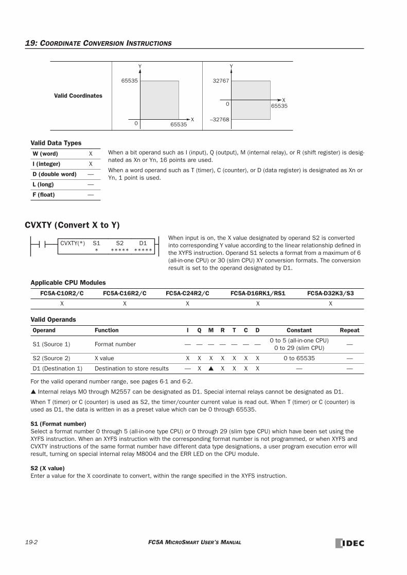
19: COORDINATE CONVERSION INSTRUCTIONS
Valid Data Types
CVXTY (Convert X to Y)
Applicable CPU Modules
Valid Operands
For the valid operand number range, see pages 6-1 and 6-2.
Internal relays M0 through M2557 can be designated as D1. Special internal relays cannot be designated as D1.
When T (timer) or C (counter) is used as S2, the timer/counter current value is read out. When T (timer) or C (counter) is used as D1, the data is written in as a preset value which can be 0 through 65535.
S1 (Format number)Select a format number 0 through 5 (all-in-one type CPU) or 0 through 29 (slim type CPU) which have been set using the XYFS instruction. When an XYFS instruction with the corresponding format number is not programmed, or when XYFS and CVXTY instructions of the same format number have different data type designations, a user program execution error will result, turning on special internal relay M8004 and the ERR LED on the CPU module.
S2 (X value)Enter a value for the X coordinate to convert, within the range specified in the XYFS instruction.
Valid Coordinates
W (word) X
I (integer) X
D (double word) —
L (long) —
F (float) —
FC5A-C10R2/C FC5A-C16R2/C FC5A-C24R2/C FC5A-D16RK1/RS1 FC5A-D32K3/S3
X X X X X
Operand Function I Q M R T C D Constant Repeat
S1 (Source 1) Format number — — — — — — —0 to 5 (all-in-one CPU)
0 to 29 (slim CPU)—
S2 (Source 2) X value X X X X X X X 0 to 65535 —
D1 (Destination 1) Destination to store results — X X X X X — —
Y
0
65535
65535X
Y
0
32767
–32768
X65535
When a bit operand such as I (input), Q (output), M (internal relay), or R (shift register) is desig-nated as Xn or Yn, 16 points are used.
When a word operand such as T (timer), C (counter), or D (data register) is designated as Xn or Yn, 1 point is used.
When input is on, the X value designated by operand S2 is converted into corresponding Y value according to the linear relationship defined in the XYFS instruction. Operand S1 selects a format from a maximum of 6 (all-in-one CPU) or 30 (slim CPU) XY conversion formats. The conversion result is set to the operand designated by D1.
CVXTY(*) S1*
S2*****
D1*****
19-2 FC5A MICROSMART USER’S MANUAL

19: COORDINATE CONVERSION INSTRUCTIONS
D1 (Destination to store results)The conversion result of the Y value is stored to the destination.
Valid Data Types
Data Conversion ErrorThe data conversion error is ±0.5.
CVYTX (Convert Y to X)
Applicable CPU Modules
Valid Operands
For the valid operand number range, see pages 6-1 and 6-2.
Internal relays M0 through M2557 can be designated as D1. Special internal relays cannot be designated as D1.
When T (timer) or C (counter) is used as S2, the timer/counter current value is read out. When T (timer) or C (counter) is used as D1, the data is written in as a preset value which can be 0 through 65535.
S1 (Format number)Select a format number 0 through 5 (all-in-one type CPU) or 0 through 29 (slim type CPU) which have been set using the XYFS instruction. When an XYFS instruction with the corresponding format number is not programmed, or when XYFS and CVYTX instructions of the same format number have different data type designations, a user program execution error will result, turning on special internal relay M8004 and the ERR LED on the CPU module.
Data Type Word Integer
S2 (X value) 0 to 65535 0 to 65535
D1 (Y value) 0 to 65535 –32768 to 32767
Valid Coordinates
W (word) X
I (integer) X
D (double word) —
L (long) —
F (float) —
FC5A-C10R2/C FC5A-C16R2/C FC5A-C24R2/C FC5A-D16RK1/RS1 FC5A-D32K3/S3
X X X X X
Operand Function I Q M R T C D Constant Repeat
S1 (Source 1) Format number — — — — — — —0 to 5 (all-in-one CPU)
0 to 29 (slim CPU)—
S2 (Source 2) Y value X X X X X X X0 to 65535
–32768 to 32767—
D1 (Destination 1) Destination to store results — X X X X X — —
Y
0
65535
65535X
Y
0
32767
–32768
X65535
When a bit operand such as I (input), Q (output), M (internal relay), or R (shift register) is desig-nated as S2 or D1, 16 points are used.
When a word operand such as T (timer), C (counter), or D (data register) is designated as S2 or D1, 1 point is used.
When input is on, the Y value designated by operand S2 is converted into corresponding X value according to the linear relationship defined in the XYFS instruction. Operand S1 selects a format from a maximum of 6 (all-in-one CPU) or 30 (slim CPU) XY conversion formats. The conversion result is set to the operand designated by D1.
CVYTX(*) S1*
S2*****
D1*****
FC5A MICROSMART USER’S MANUAL 19-3

19: COORDINATE CONVERSION INSTRUCTIONS
S2 (Y value)Enter a value for the Y coordinate to convert, within the range specified in the XYFS instruction. Two different data ranges are available depending on the data type.
D1 (Destination to store results)The conversion result of the X value is stored to the destination.
Valid Data Types
Data Conversion ErrorThe data conversion error is ±0.5.
Data Type Word Integer
S2 (Y value) 0 to 65535 –32768 to 32767
D1 (X value) 0 to 65535 0 to 65535
Valid Coordinates
W (word) X
I (integer) X
D (double word) —
L (long) —
F (float) —
Y
0
65535
65535X
Y
0
32767
–32768
X65535
When a bit operand such as I (input), Q (output), M (internal relay), or R (shift register) is desig-nated as S2 or D1, 16 points are used.
When a word operand such as T (timer), C (counter), or D (data register) is designated as S2 or D1, 1 point (integer data type) is used.
19-4 FC5A MICROSMART USER’S MANUAL

19: COORDINATE CONVERSION INSTRUCTIONS
Example: Linear ConversionThe following example demonstrates setting up two coordinate points to define the linear relationship between X and Y. The two points are (X0, Y0) = (0, 0) and (X1, Y1) = (8000, 4000). Once these are set, there is an X to Y conversion, as well as a Y to X conversion.
M8120 is the initialize pulse special internal relay.
At startup, XYFS specifies two points.
When input I0 is on, CVXTY converts the value in D10 and stores the result in D20.
When input I1 is on, CVYTX converts the value in D11 and stores the result in D21.
M8120XYFS(I) Y1
4000
END
I0CVXTY(I) D1
D20
I1CVYTX(I) S1
D21
S10
X00
Y00
X18000
S10
S2D10
S10
S2D11
(X0, Y0)
(X1, Y1)
X
Y
0D10 D21
D20 (1000)
D11 (2500)
The graph shows the linear relationship that is defined by the two points:
If the value in data register D10 is 2000, the value assigned to D20 is 1000.
For Y to X conversion, the following equation is used:
If the value in data register D11 is 2500, the value assigned to D21 is 5000.
Y 12---X=
X 2Y=8000
(2000) (5000)
FC5A MICROSMART USER’S MANUAL 19-5

19: COORDINATE CONVERSION INSTRUCTIONS
Example: Overlapping CoordinatesIn this example, the XYFS instruction sets up three coordinate points, which define two different linear relationships between X and Y. The three points are: (X0, Y0) = (0, 100), (X1, Y1) = (100, 0), and (X2, Y2) = (300, 100). The two line segments define overlapping coordinates for X. That is, for each value of Y within the designated range, there would be two X values assigned.
The first line segment defines the following relationship for X to Y conversion:
The second line segment defines another relationship for X to Y conversion:
For X to Y conversion, each value of X has only one corresponding value for Y. If the current value of counter C10 is 250, the value assigned to D90 is 75.
For Y to X conversion, the XYFS instruction assigns two possible values of X for each value of Y. The relationship defined by the first two points has priority in these cases. The line between points (X0, Y0) and (X1, Y1), that is, the line between (0, 100) and (100, 0), has priority in defining the relationship for Y to X conversion (X = –Y + 100).
Therefore, if the value in data register D95 is 40, the value assigned to D30 is 60, not 180.
Exactly the same two line segments might also be defined by the XYFS instruction, except that the point (300, 100) could be assigned first, as (X0, Y0), and the point (100, 0) could be defined next, as (X1, Y1). In this case, this linear relationship would have priority.
In this case, if the value in data register D95 is 40, the value assigned to D30 is 180, not 60.
M8120 is the initialize pulse special internal relay.
At startup, XYFS specifies three points.
CVXTY converts the value in C10 and stores the result in D90.
CVYTX converts the value in D95 and stores the result in D30.
M8120XYFS(I) Y2
100
END
I0CVXTY(I) D1
D90
I1CVYTX(I) S1
D30
S10
X00
Y0100
X1100
S10
S2C10
S10
S2D95
X
Y
0D30 C10
D95 (40)
D90 (75)
300
Y10
X2300
100
(X0, Y0)(0, 100)
(X1, Y1)(100, 0)
(X2, Y2)(300, 100)
100(60) (250)
Y X– 100+=
Y 12---X 50–=
19-6 FC5A MICROSMART USER’S MANUAL

19: COORDINATE CONVERSION INSTRUCTIONS
AVRG (Average)
The AVRG instruction is effective for data processing of analog input values. A maximum of 32 AVRG instructions can be pro-grammed in a user program.
Applicable CPU Modules
Valid Operands
For the valid operand number range, see pages 6-1 and 6-2.
Internal relays M0 through M2557 can be designated as D2. Special internal relays cannot be designated as D2. When T (timer) or C (counter) is used as S1 or S3, the timer/counter current value is read out.
When F (float) data type is selected, only data registers can be designated as S1 and D1.
While input is on, the AVRG instruction is executed in each scan. When the quantity of sampling cycles (scan times) desig-nated by operand S3 is 1 through 65535, sampling data designated by operand S1 is processed in each scan. When the designated sampling cycles have been completed, the average value of the sampling data is set to operand designated by D1 (data type W or I) or D1·D1+1 (data type D, L, or F). The maximum value of the sampling data is set to the next operand, D1+1 (data type W or I) or D1+2·D1+3 (data type D, L, or F). The minimum value of the sampling data is set to the next oper-and, D1+2 (data type W or I) or D1+4·D1+5 (data type D, L, or F). The sampling completion output designated by operand D2 is turned on.
When the quantity of sampling cycles designated by operand S3 is 0, sampling is started when the input to the AVRG instruction is turned on, and stopped when the sampling end input designated by operand S2 is turned on. Then, the aver-age, maximum, and minimum values are set to 3 operands starting with operand designated by D1.
When the sampling exceeds 65535 cycles, the average, maximum, and minimum values at this point are set to 3 operands starting with operand designated by D1, and sampling continues.
When the sampling end input is turned on before the sampling cycles designated by operand S3 have been completed, sam-pling is stopped and the results at this point are set to 3 operands starting with operand designated by D1.
The average value is calculated to units, rounding the fractions of one decimal place.
When the sampling end input is not used, designate an internal relay or another valid operand as a dummy for source oper-and S2.
When F (float) data type is selected and S1 does not comply with the normal floating-point format, a user program execution error will result, turning on special internal relay M8004 and ERR LED on the CPU module. When an error occurs, incorrect S1 data are skipped. Average, maximum, and minimum values are calculated from correct S1 data, and set to 3 operands starting with operand designated by D1.
FC5A-C10R2/C FC5A-C16R2/C FC5A-C24R2/C FC5A-D16RK1/RS1 FC5A-D32K3/S3
X X X X X
Operand Function I Q M R T C D Constant Repeat
S1 (Source 1) Sampling data X X X X X X X — —
S2 (Source 2) Sampling end input X X X X — — — — —
S3 (Source 3) Sampling cycles (scan times) X X X X X X X 0-65535 —
D1 (Destination 1) First operand number to store results — — — — — — X — —
D2 (Destination 2) Sampling completion output — X — — — — — —
When input is on, sampling data designated by oper-and S1 is processed according to sampling conditions designated by operands S2 and S3.
When sampling is complete, average, maximum, and minimum values are stored to 3 consecutive operands starting with operand designated by D1, then sampling completion output designated by operand D2 is turned on.
Data Type W, I D, L, FAverage D1 D1·D1+1Maximum value D1+1 D1+2·D1+3Minimum value D1+2 D1+4·D1+5
AVRG(*) S1*****
S3*****
D1*****
S2*****
D2*****
FC5A MICROSMART USER’S MANUAL 19-7

19: COORDINATE CONVERSION INSTRUCTIONS
Valid Data Types
Example: AVRGThe following example demonstrates a program to calculate average values of the data register D100 and store the result to data register D200 in every 500 scans.
When the sampling end input does not turn onWhile sampling end input I10 is off, the average, maximum, and minimum values are calculated in every 500 scans and stored to data registers D200, D201, and D202, respectively. Sampling completion output M100 is set every 500 scans.
When the sampling end input turns onWhen sampling end input I10 turns on, the average, maximum, and minimum values at this point are stored to data regis-ters D200, D201, and D202, respectively. Sampling completion output M100 is also set. When sampling end input I10 turns off, sampling resumes starting at the first scan.
W (word) X
I (integer) X
D (double word) X
L (long) X
F (float) X
When a bit operand such as I (input), Q (output), M (internal relay), or R (shift register) is desig-nated as the source, 16 points (word or integer data type) or 32 points (double-word or long data type) are used.
When a word operand such as T (timer), C (counter), or D (data register) is designated as the source, 1 point (word or integer data type) or 2 points (double-word, long, or float data type) are used.
M8125 is the in-operation output special internal relay.
M8125S1
D100S2I10
AVRG(W) D2M100
S3500
D1D200
512
1st scan
497
2nd scan
521
500th scan
499
1st scan
478
2nd scan
In-operation Special IR M8125ON
OFF
Sampling End Input I10ON
OFF
Sampling Completion Output M100ON
OFF
Sampling Data D100
Average Value D200 500
Maximum Value D201 530
Minimum Value D202 480
Values are set every 500 scans.
489
151st scan
510
152nd scan
509
153rd scan
504
XXXth scan
493
1st scan
In-operation Special IR M8125ON
OFF
Sampling End Input I10ON
OFF
Sampling Completion Output M100ON
OFF
Sampling Data D100
Average Value D200 502
Maximum Value D201 513
Minimum Value D202 485
Values are set when I10 is turned on.
19-8 FC5A MICROSMART USER’S MANUAL
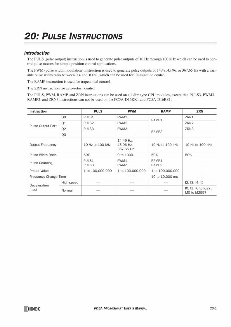
20: PULSE INSTRUCTIONS
IntroductionThe PULS (pulse output) instruction is used to generate pulse outputs of 10 Hz through 100 kHz which can be used to con-trol pulse motors for simple position control applications.
The PWM (pulse width modulation) instruction is used to generate pulse outputs of 14.49, 45.96, or 367.65 Hz with a vari-able pulse width ratio between 0% and 100%, which can be used for illumination control.
The RAMP instruction is used for trapezoidal control.
The ZRN instruction for zero-return control.
The PULS, PWM, RAMP, and ZRN instructions can be used on all slim type CPU modules, except that PULS3, PWM3, RAMP2, and ZRN3 instructions can not be used on the FC5A-D16RK1 and FC5A-D16RS1.
Instruction PULS PWM RAMP ZRN
Pulse Output Port
Q0 PULS1 PWM1RAMP1
ZRN1
Q1 PULS2 PWM2 ZRN2
Q2 PULS3 PWM3RAMP2
ZRN3
Q3 — — —
Output Frequency 10 Hz to 100 kHz14.49 Hz, 45.96 Hz, 367.65 Hz
10 Hz to 100 kHz 10 Hz to 100 kHz
Pulse Width Ratio 50% 0 to 100% 50% 50%
Pulse CountingPULS1PULS3
PWM1PWM3
RAMP1RAMP2
—
Preset Value 1 to 100,000,000 1 to 100,000,000 1 to 100,000,000 —
Frequency Change Time — — 10 to 10,000 ms —
Deceleration Input
High-speed — — — I2, I3, I4, I5
Normal — — —I0, I1, I6 to I627, M0 to M2557
FC5A MICROSMART USER’S MANUAL 20-1

20: PULSE INSTRUCTIONS
PULS1 (Pulse Output 1)
PULS2 (Pulse Output 2)
PULS3 (Pulse Output 3)
Note: The PULS1, PULS2, and PULS3 instructions can be used only once in a user program. When PULS1, PULS2, or PULS3 is not used, unused output Q0, Q1, or Q2 can be used for another pulse instruction or ordinary output.
Applicable CPU Modules
Valid Operands
Source operand S1 (control register) uses 8 data registers starting with the operand designated as S1. Data registers D0-D1992, D2000-D7992, and D10000-D49992 can be designated as S1. For details, see the following pages.
Destination operand D1 (status relay) uses 3 internal relays starting with the operand designated as D1. Internal relays M0 to M2550 can be designated as D1. The least significant digit of the internal relay number designated as D1 must be 0, oth-erwise the PULS instruction does not operate correctly. Special internal relays cannot be designated as D1. For details, see page 6-2.
Source Operand S1 (Control Register)Store appropriate values to data registers starting with the operand designated by S1 before executing the PULS instruction as required, and make sure that the values are within the valid range. Operands S1+5 through S1+7 are for read only.
FC5A-C10R2/C FC5A-C16R2/C FC5A-C24R2/C FC5A-D16RK1/RS1 FC5A-D32K3/S3
— — — X (PULS1 and PULS2) X
Operand Function I Q M R T C D Constant Repeat
S1 (Source 1) Control register — — — — — — X — —
D1 (Destination 1) Status relay — — X — — — — — —
Operand Function Description R/W
S1+0 Operation mode
0: 10 Hz to 1 kHz 1: 100 Hz to 10 kHz 2: 1 kHz to 100 kHz 3: 200 Hz to 100 kHz
R/W
S1+1 Output pulse frequencyWhen S1+0 (operation mode) = 0 to 2: 1 to 100 (%) (1% to 100% of the maximum frequency of selected mode S1+0)When S1+0 (operation mode) = 3: 20 to 10,000 (×10 Hz)
R/W
When input is on, the PULS1 instruction sends out a pulse output from output Q0. The output pulse frequency is determined by source operand S1. The output pulse width ratio is fixed at 50%.
PULS1 can be programmed to generate a predetermined number of output pulses. When pulse counting is disabled, PULS1 generates output pulses while the start input for the PULS1 instruction remains on.
PULS1
S1*****
D1*****
When input is on, the PULS2 instruction sends out a pulse output from output Q1. The output pulse frequency is determined by source operand S1. The output pulse width ratio is fixed at 50%.
PULS2 generates output pulses while the start input for the PULS2 instruction remains on. PULS2 cannot be programmed to generate a predetermined number of output pulses.
PULS2
S1*****
D1*****
When input is on, the PULS3 instruction sends out a pulse output from output Q2. The output pulse frequency is determined by source operand S1. The output pulse width ratio is fixed at 50%.
PULS3 can be programmed to generate a predetermined number of output pulses. When pulse counting is disabled, PULS3 generates output pulses while the start input for the PULS3 instruction remains on.
PULS3
S1*****
D1*****
Not available on FC5A-16RK1/RS1
20-2 FC5A MICROSMART USER’S MANUAL

20: PULSE INSTRUCTIONS
S1+0 Operation Mode
The value stored in the data register designated by operand S1+0 determines the frequency range of the pulse output.
0: 10 Hz to 1 kHz
1: 100 Hz to 10 kHz
2: 1 kHz to 100 kHz
3: 200 Hz to 100 kHz
S1+1 Output Pulse Frequency
When S1+0 is set to 0 through 2, the value stored in the data register designated by operand S1+1 specifies the frequency of the pulse output in percent of the maximum of the frequency range selected by S1+0. Valid values for operand S1+1 are 1 through 100, thus the output pulse frequency can be 10 Hz to 1 kHz (operation mode 0), 100 Hz to 10 kHz (operation mode 1), or 1 kHz to 100 kHz (operation mode 2).
When S1+0 is set to 3 (200 Hz to 100 kHz), valid values for operand S1+1 are 20 through 10,000 and the S1+1 value mul-tiplied by 10 determines the output pulse frequency, thus the output pulse frequency can be 200 Hz to 100 kHz. The output frequency error is ±5% maximum.
S1+2 Pulse Counting
Pulse counting can be enabled for the PULS1 and PULS3 instruction only. With pulse counting enabled, PULS1 or PULS3 generates a predetermined number of output pulses as designated by operands S1+3 and S1+4. With pulse counting dis-abled, PULS1, PULS2, or PULS3 generates output pulses while the start input for the PULS instruction remains on.
0: Disable pulse counting
1: Enable pulse counting (PULS1/PULS3 only)
When programming PULS2, store 0 to the data register designated by S1+2.
S1+3 Preset Value (High Word) S1+4 Preset Value (Low Word)
With pulse counting enabled as described above, PULS1 or PULS3 generates a predetermined number of output pulses as designated by operands S1+3 and S1+4. The preset value can be 1 through 100,000,000 (05F5 E100h) stored in two con-secutive data registers designated by S1+3 (high word) and S1+4 (low word).
When pulse counting is disabled for PULS1 or PULS3 or when programming PULS2, store 0 to data registers designated by S1+3 and S1+4.
S1+5 Current Value (High Word) S1+6 Current Value (Low Word)
While the PULS1 or PULS3 instruction is executed with pulse counting enabled, the output pulse count is stored in two consecutive data registers designated by operands S1+5 (high word) and S1+6 (low word). The current value can be 1 through 100,000,000 (05F5 E100h) and is updated in every scan.
S1+2 Pulse counting0: Disable pulse counting 1: Enable pulse counting (PULS1/PULS3 only)
R/W
S1+3 Preset value (high word)1 to 100,000,000 (05F5 E100h) (PULS1/PULS3 only) R/W
S1+4 Preset value (low word)
S1+5 Current value (high word)1 to 100,000,000 (05F5 E100h) (PULS1/PULS3 only) R
S1+6 Current value (low word)
S1+7 Error status 0 to 5 R
Operation Mode (S1+0) S1+1 Output Pulse Frequency (Hz)
0 to 2 1 to 100 Maximum frequency selected by S1+0 × S1+1 value (%)
3 20 to 10,000 S1+1 value × 10
Operand Function Description R/W
FC5A MICROSMART USER’S MANUAL 20-3

20: PULSE INSTRUCTIONS
S1+7 Error Status
When the start input for the PULS instruction is turned on, operand values are checked. When any error is found in the operand values, the data register designated by operand S1+7 stores an error code.
Destination Operand D1 (Status Relay)Three internal relays starting with the operand designated by D1 indicate the status of the PULS instruction. These oper-ands are for read only.
D1+0 Pulse Output ON
The internal relay designated by operand D1+0 remains on while the PULS instruction generates output pulses. When the start input for the PULS instruction is turned off or when the PULS1 or PULS3 instruction has completed generating a pre-determined number of output pulses, the internal relay designated by operand D1+0 turns off.
D1+1 Pulse Output Complete
The internal relay designated by operand D1+1 turns on when the PULS1 or PULS3 instruction has completed generating a predetermined number of output pulses or when either PULS instruction is stopped to generate output pulses. When the start input for the PULS instruction is turned on, the internal relay designated by operand D1+1 turns off.
D1+2 Pulse Output Overflow
The internal relay designated by operand D1+2 turns on when the PULS1 or PULS3 instruction has generated more than the predetermined number of output pulses. When the start input for the PULS instruction is turned on, the internal relay designated by operand D1+2 turns off.
Special Data Registers for Pulse OutputsThree additional special data registers store the current frequency of pulse outputs.
Error Code Description
0 Normal
1 Operation mode designation error (S1+0 stores other than 0 through 3)
2Output pulse frequency designation error Mode 0 to 2: S1+1 stores other than 1 through 100 Mode 3: S1+1 stores other than 20 through 10,000
3 Pulse counting designation error (S1+2 stores other than 0 and 1)
4 Preset value designation error (S1+3 and S1+4 store other than 1 through 100,000,000)
5 Invalid pulse counting designation for PULS2 (S1+2 stores 1)
Operand Function Description R/W
D1+0 Pulse output ON0: Pulse output OFF 1: Pulse output ON
R
D1+1 Pulse output complete0: Pulse output not complete 1: Pulse output complete
R
D1+2 Pulse output overflow0: Overflow not occurred 1: Overflow occurred (PULS1/PULS3 only)
R
Allocation No. Function Description
D8055Current Pulse Frequency of PULS1 or RAMP1 (Q0)
While the PULS1 or RAMP1 instruction is executed, D8055 stores the cur-rent pulse frequency of output Q0. The value is updated every scan.
D8056Current Pulse Frequency of PULS2 or RAMP1 (Q1)
While the PULS2 or RAMP1 (reversible control dual-pulse output) instruc-tion is executed, D8056 stores the current pulse frequency of output Q1. The value is updated every scan.
D8059Current Pulse Frequency of PULS3 or RAMP2 (Q2)
While the PULS3 or RAMP2 instruction is executed, D8059 stores the cur-rent pulse frequency of output Q2. The value is updated every scan.
20-4 FC5A MICROSMART USER’S MANUAL

20: PULSE INSTRUCTIONS
Timing Chart for Enable Pulse CountingThis program demonstrates a timing chart of the PULS1 instruction when pulse counting is enabled.
D1M50I0
PULS1
S1D200
D202 = 1 (enable pulse counting)
Output Pulse Q0
Output Pulse Frequency D201
PV1
FR1
Start Input I0
• When input I0 is turned on, PULS1 starts to generate output pulses at the frequency designated by the value stored in data register D201. While the output pulses are sent out from output Q0, internal relay M50 remains on.
• When the quantity of generated output pulses reaches the preset value designated by data registers D203 and D204, PULS1 stops generating output pulses. Then internal relay M50 turns off, and internal relay M51 turns on.
• If the output pulse frequency value in D201 is changed while generating output pulses, the change takes effect in the next scan. When changing the pulse frequency, make sure that the timing of the change is much slower than the output pulse frequency, so that the pulse frequency is changed successfully.
• If input I0 is turned off before reaching the preset value, PULS1 stops generating output pulses immediately, then internal relay M50 turns off and internal relay M51 turns on.
FR2 FR3
Preset Value D203·D204 PV1 PV2 PV3
Pulse Output ON M50
Pulse Output Complete M51
PV2
FC5A MICROSMART USER’S MANUAL 20-5

20: PULSE INSTRUCTIONS
Timing Chart for Disable Pulse CountingThis program demonstrates a timing chart of the PULS2 instruction without pulse counting.
D1M20I1
PULS2
S1D100
D102 = 0 (disable pulse counting)
Output Pulse Q1
Output Pulse Frequency D101
FR1
FR1
Start Input I1
• When input I1 is turned on, PULS2 starts to generate output pulses at the frequency designated by the value stored in data register D101. While the output pulses are sent out from output Q1, internal relay M20 remains on.
• When input I1 is turned off, PULS2 stops generating output pulses immediately, then internal relay M20 turns off and internal relay M21 turns on.
• If the output pulse frequency value in D101 is changed while generating output pulses, the change takes effect in the next scan. When changing the pulse frequency, make sure that the timing of the change is much slower than the output pulse frequency, so that the pulse frequency is changed successfully.
FR2 FR3
Pulse Output ON M20
Pulse Output Complete M21
FR2
20-6 FC5A MICROSMART USER’S MANUAL

20: PULSE INSTRUCTIONS
Sample Program: PULS1This program demonstrates a user program of the PULS1 instruction to generate 5,000 pulses at a frequency of 200 Hz from output Q0, followed by 60,000 pulses at a frequency of 500 Hz.
Programming WindLDR
On the WindLDR editing screen, place the cursor where you want to insert the pulse instruction macro, and type PULSST. Enter parameters as shown below.
Operand SettingsOperand Function Description Allocation No. (Value)
S1+0 Operation mode Frequency range 200 Hz to 100 kHz D0 (3)S1+1 Output pulse frequency 200 Hz D1 (20)S1+2 Pulse counting Enable pulse counting D2 (1)S1+3 Preset value (high word)
5,000 D3/D4 (5000)S1+4 Preset value (low word)S1+5 Current value (high word)
0 to 60,000 D5/D6S1+6 Current value (low word)
Same operand as S1 for the PULS1
instruction
M8120
REPS1 –50
MOV(W) D1 –D1M101
SOTU
M8120 is the initialize pulse special internal relay.
When the CPU starts, PULSST macro designates parameters for pulse output in the first stage.
Pulse data update flag M1 is reset (pulse data not updated).
Pulse output complete flag M101 is turned off.
When M101 is turned on, two MOV instructions store second-stage parameters to data registers D1, D3, and D4.
D1 (output pulse frequency): 50 (500 Hz)
D3/D4 (preset value): 60,000
Pulse data update flag M1 is set (pulse data updated).
When start input I0 is turned on, PULS1 starts to generate 5,000 output pulses at 200Hz in the first stage.
Pulse output complete M101 is turned off.
I0
SOTUM1
S1D0
PULSST
M1S
M1R
M101R
REPS1 –60000
MOV(D) D1 –D3
M101R
M101D1
M100PULS1
S1D0
FC5A MICROSMART USER’S MANUAL 20-7

20: PULSE INSTRUCTIONS
PWM1 (Pulse Width Modulation 1)
PWM2 (Pulse Width Modulation 2)
PWM3 (Pulse Width Modulation 3)
Note: The PWM1, PWM2, and PWM3 instructions can be used only once in a user program. When PWM1, PWM2, or PWM3 is not used, unused output Q0, Q1, or Q2 can be used for another pulse instruction or ordinary output.
Applicable CPU Modules
Valid Operands
Source operand S1 (control register) uses 8 data registers starting with the operand designated as S1. Data registers D0-D1992, D2000-D7992, and D10000-D49992 can be designated as S1. For details, see the following pages.
Destination operand D1 (status relay) uses 3 internal relays starting with the operand designated as D1. Internal relays M0 to M2550 can be designated as D1. The least significant digit of the internal relay number designated as D1 must be 0, oth-erwise the PWM instruction does not operate correctly. Special internal relays cannot be designated as D1. For details, see page 6-2.
FC5A-C10R2/C FC5A-C16R2/C FC5A-C24R2/C FC5A-D16RK1/RS1 FC5A-D32K3/S3
— — — X (PWM1 and PWM2) X
Operand Function I Q M R T C D Constant Repeat
S1 (Source 1) Control register — — — — — — X — —
D1 (Destination 1) Status relay — — X — — — — — —
When input is on, the PWM1 instruction generates a pulse output. The output pulse frequency is selected from 14.49, 45.96, or 367.65 Hz, and the output pulse width ratio is determined by source operand S1.
PWM1 sends out output pulses from output Q0.
PWM1 can be programmed to generate a predetermined number of output pulses. When pulse counting is disabled, PWM1 generates output pulses while the start input for the PWM1 instruction remains on.
PWM1
S1*****
D1*****
When input is on, the PWM2 instruction generates a pulse output. The output pulse frequency is selected from 14.49, 45.96, or 367.65 Hz, and the output pulse width ratio is determined by source operand S1.
PWM2 sends out output pulses from output Q1.
PWM2 generates output pulses while the start input for the PWM2 instruction remains on. PWM2 cannot be programmed to generate a predetermined number of output pulses.
PWM2
S1*****
D1*****
When input is on, the PWM3 instruction generates a pulse output. The output pulse frequency is selected from 14.49, 45.96, or 367.65 Hz, and the output pulse width ratio is determined by source operand S1.
PWM3 sends out output pulses from output Q2.
PWM3 can be programmed to generate a predetermined number of output pulses. When pulse counting is disabled, PWM3 generates output pulses while the start input for the PWM3 instruction remains on.
PWM3
S1*****
D1*****
Not available on FC5A-16RK1/RS1
20-8 FC5A MICROSMART USER’S MANUAL

20: PULSE INSTRUCTIONS
Source Operand S1 (Control Register)Store appropriate values to data registers starting with the operand designated by S1 before executing the PWM instruction as required, and make sure that the values are within the valid range. Operands S1+5 through S1+7 are for read only.
S1+0 Output Pulse Frequency
The value stored in the data register designated by operand S1+0 determines the pulse output frequency.
0: 14.49 Hz (69.01 ms period)
1: 45.96 Hz (21.76 ms period)
2: 367.65 Hz (2.72 ms period)
S1+1 Pulse Width Ratio
The value stored in the data register designated by operand S1+1 specifies the pulse width ratio of the pulse output in per-cent of the period determined by the output pulse frequency selected with S1+0. Valid values for operand S1+1 are 1 through 100.
S1+2 Pulse Counting
Pulse counting can be enabled for the PWM1 and PWM3 instructions only. With pulse counting enabled, PWM1 or PWM3 generates a predetermined number of output pulses as designated by operands S1+3 and S1+4. With pulse count-ing disabled, the PWM instruction generates output pulses while the start input for the PWM instruction remains on.
0: Disable pulse counting
1: Enable pulse counting (PWM1/PWM3 only)
When programming PWM2, store 0 to the data register designated by S1+2.
S1+3 Preset Value (High Word) S1+4 Preset Value (Low Word)
With pulse counting enabled as described above, PWM1 or PWM3 generates a predetermined number of output pulses as designated by operands S1+3 and S1+4. The preset value can be 1 through 100,000,000 (05F5 E100h) stored in two con-secutive data registers designated by S1+3 (high word) and S1+4 (low word).
When pulse counting is disabled for PWM1 or PWM3 or when programming PWM2, store 0 to data registers designated by S1+3 and S1+4.
Operand Function Description R/W
S1+0 Output pulse frequency0: 14.49 Hz 1: 45.96 Hz 2: 367.65 Hz
R/W
S1+1 Pulse width ratio1 to 100 (1% to 100% of the period determined by output pulse frequency S1+0)
R/W
S1+2 Pulse counting0: Disable pulse counting 1: Enable pulse counting (PWM1/PWM3 only)
R/W
S1+3 Preset value (high word)1 to 100,000,000 (05F5 E100h) (PWM1/PWM3 only) R/W
S1+4 Preset value (low word)S1+5 Current value (high word)
1 to 100,000,000 (05F5 E100h) (PWM1/PWM3 only) RS1+6 Current value (low word)S1+7 Error status 0 to 5 R
Pulse Width = Period × Pulse Width Ratio (%)
Pulse Width Period Pulse Width Ratio 100
- - - - - - - - - - - - - - - - - - - - - - - - - - - - - - - - - - - - - - - - - - - - - - × =
1
Output Pulse Frequency -
-
-
-
-
-
-
-
-
-
-
-
-
-
-
-
-
-
-
-
-
-
-
-
-
-
-
-
-
-
-
-
-
-
-
-
-
-
-
-
-
-
-
-
-
-
-
-
-
-
-
-
-
-
-
-
-
-
-
-
-
-
Pulse Width Ratio
100 - - - - - - - - - - - - - - - - - - - - - - - - - - - - - - - - - - - - - - - - - - - - - - × =
Period (69.01, 21.76, or 2.72 ms)
FC5A MICROSMART USER’S MANUAL 20-9

20: PULSE INSTRUCTIONS
S1+5
Current Value (High Word) S1+6 Current Value (Low Word)
While the PWM1 or PWM3 instruction is e
xecuted, the output pulse count is stored in two consecutive data registers des-ignated by operands S1+5 (high word) and S1+6 (low word). The current value can be 1 through 100,000,000 (05F5 E100h) and is updated in every scan.
S1+7
Error Status
When the start input for the PWM instruction is turned on, operand v
alues are checked. When any error is found in the operand values, the data register designated by operand S1+7 stores an error code.
Destination Operand D1 (
Status Relay)
Three internal relays starting with the operand designated by D1 indicate the status of the PWM instruction.
These oper-ands are for read only.
D1+0 Pulse Output ON
The internal relay designated by operand D1+0 remains on while the PWM instruction generates output pulses.
When the start input for the PWM instruction is turned off or when the PWM1 or PWM3 instruction has completed generating a pre-determined number of output pulses, the internal relay designated by operand D1+0 turns off.
D1+1
Pulse Output Complete
The internal relay designated by operand D1+1 turns on when the PWM1 or PWM3 instruction has completed generating
a predetermined number of output pulses or when either PWM instruction is stopped to generate output pulses. When the start input for the PWM instruction is turned on, the internal relay designated by operand D1+1 turns off.
D1+2
Pulse Output Overflow
The internal relay designated by operand D1+2 turns on when the PWM1 or PWM3 instruction has generated more than
the predetermined number of output pulses. When the start input for the PWM instruction is turned on, the internal relay designated by operand D1+2 turns off.
Er
ror Code Description
0
Nor
mal
1 Output pulse frequency designation error (S1+0 stores other than 0 through 2)
2 Pulse width ratio designation error (S1+1 stores other than 1 through 100)
3 Pulse counting designation error (S1+2 stores other than 0 and 1)
4 Preset value designation error (S1+3 and S1+4 store other than 1 through 100,000,000)
5 Invalid pulse counting designation for PWM2 (S1+2 stores 1)
Operand Function Description R/W
D1+0 Pulse output ON0: Pulse output OFF 1: Pulse output ON
R
D1+1 Pulse output complete0: Pulse output not complete 1: Pulse output complete
R
D1+2 Pulse output overflow0: Overflow not occurred 1: Overflow occurred (PWM1/PWM3 only)
R
20-10 FC5A MICROSMART USER’S MANUAL

20: PULSE
I
NSTRUCTIONS
Timing Chart for Enable Pulse CountingThis program demonstrates a timing chart of the PWM1 instruction when pulse counting is enabled.
D1M50I0
PWM1
S1D200
D202 = 1 (enable pulse counting)
• When input I0 is turned on, PWM1 starts to generate output pulses at the frequency designated by the value stored in data register D200. The pulse width is determined by the value stored in data register D201. While the output pulses are sent out from output Q0, internal relay M50 remains on.
• When the quantity of generated output pulses reaches the preset value designated by data registers D203 and D204, PWM1 stops generating output pulses. Then internal relay M50 turns off, and internal relay M51 turns on.
• If the pulse width ratio value in D201 is changed while generating output pulses, the change takes effect in the next scan. When changing the pulse width ratio, make sure that the timing of the change is much slower than the output pulse frequency, so that the pulse width ratio is changed successfully.
• If input I0 is turned off before reaching the preset value, PWM1 stops generating output pulses immediately, then internal relay M50 turns off and internal relay M51 turns on.
Output Pulse Q0
Pulse Width Ratio D201
PV1
PWR1
Start Input I0
PWR2 PWR3
Preset Value D203·D204 PV1 PV2 PV3
Pulse Output ON M50
Pulse Output Complete M51
PV2
PWR1 PWR2
FC5A MICROSMART USER’S MANUAL 20-11

20: PULSE INSTRUCTIONS
Timing Chart for Disable Pulse CountingThis program demonstrates a timing chart of the PWM2 instruction without pulse counting.
D1M20I1
PWM2
S1D100
D102 = 0 (disable pulse counting)
Output Pulse Q1
Pulse Width Ratio D101 PWR1
Start Input I1
• When input I1 is turned on, PWM2 starts to generate output pulses at the frequency designated by the value stored in data register D100. The pulse width is determined by the value stored in data register D101. While the output pulses are sent out from output Q1, internal relay M20 remains on.
• When input I1 is turned off, PWM2 stops generating output pulses immediately, then internal relay M20 turns off and internal relay M21 turns on.
• If the pulse width ratio value in D101 is changed while generating output pulses, the change takes effect in the next scan. When changing the pulse width ratio, make sure that the timing of the change is much slower than the output pulse frequency, so that the pulse width ratio is changed successfully.
PWR2 PWR3
Pulse Output ON M20
Pulse Output Complete M21
PWR1 PWR2
20-12 FC5A MICROSMART USER’S MANUAL

20: PULSE INSTRUCTIONS
Sample Program: PWM2This program demonstrates a user program of the PWM2 instruction to generate pulses from output Q1, with an ON/OFF ratio of 30% while input I0 is off or 60% when input I0 is on.
Programming WindLDR
On the WindLDR editing screen, place the cursor where you want to insert the pulse instruction macro, and type PWMST. Enter parameters as shown below.
Operand SettingsOperand Function Description Allocation No. (Value)
S1+0 Output pulse frequency 367.65 Hz D0 (2)S1+1 Pulse width ratio 30% D1 (30)S1+2 Pulse counting Disable pulse counting D2 (0)S1+3 Preset value (high word)
Not usedD3
S1+4 Preset value (low word) D4S1+5 Current value (high word)
Not usedD5
S1+6 Current value (low word) D6S1+7 Error status D7
D1+0 Pulse output ON0: Pulse output OFF 1: Pulse output ON
M100
D1+1 Pulse output complete0: Pulse output not complete 1: Pulse output complete
M101
D1+2 Pulse output overflow0: Overflow not occurred 1: Overflow occurred (PWM1/PWM3 only)
M102
Same operand as S1 for the PWM2
instruction
M8120
I0
M8120 is the initialize pulse special internal relay.
When the CPU starts, PWMST macro designates parameters for pulse out-put in the first stage.
When input I0 is off, D1 (pulse width ratio) stores 30 (30%).
When input I0 is on, D1 (pulse width ratio) stores 60 (60%).
When input I1 is on, PWM2 generates output pulses of a 30% or 60% pulse width ratio from output Q1 depending whether input I0 is off or on, respectively.
REPS1 –30
MOV(W) D1 –D1
REPS1 –60
MOV(W) D1 –D1
I0
D1M100
PWM2
S1D0I1
S1D0
PWMST
FC5A MICROSMART USER’S MANUAL 20-13

20: PULSE INSTRUCTIONS
RAMP1 (Ramp Control 1)
Note: The RAMP1 instruction can be used only once in a user program. When RAMP1 is used with reversible control dis-abled, unused output Q1 can be used for another pulse instruction PULS2, PWM2, or ZRN2 or ordinary output.
RAMP2 (Ramp Control 2)
Note: The RAMP2 instruction can be used only once in a user program.
Applicable CPU Modules
Valid Operands
Source operand S1 (control register) uses 11 data registers starting with the operand designated as S1. Data registers D0-D1989, D2000-D7989, and D10000-D49989 can be designated as S1. For details, see the following pages.
Destination operand D1 (status relay) uses 4 internal relays starting with the operand designated as D1. Internal relays M0 to M2550 can be designated as D1. The least significant digit of the internal relay number designated as D1 must be 0, oth-erwise the RAMP instruction does not operate correctly. Special internal relays cannot be designated as D1. For details, see page 6-2.
Source Operand S1 (Control Register)Store appropriate values to data registers starting with the operand designated as S1 before executing the RAMP instruc-tion as required, and make sure that the values are within the valid range. Operands S1+8 through S1+10 are for read only.
FC5A-C10R2/C FC5A-C16R2/C FC5A-C24R2/C FC5A-D16RK1/RS1 FC5A-D32K3/S3
— — — X (RAMP1) X
Operand Function I Q M R T C D Constant Repeat
S1 (Source 1) Control register — — — — — — X — —
D1 (Destination 1) Status relay — — X — — — — — —
Operand Function Description R/W
S1+0 Operation mode
0: 10 Hz to 1 kHz 1: 100 Hz to 10 kHz 2: 1 kHz to 100 kHz 3: 200 Hz to 100 kHz
R/W
When input is on, the RAMP1 instruction sends out a predetermined number of output pulses from output Q0. The output frequency changes in a trapezoidal pat-tern determined by source operand S1. After starting the RAMP1 instruction, the output pulse frequency increases linearly to a predetermined constant value, remains constant at this value for some time, and then decreases linearly to the original value.
The frequency change rate or the frequency change time can be selected for acceleration and deceleration of the movement.
When input is off, the pulse output remains off. When input is turned on again, the RAMP1 instruction starts a new cycle of generating output pulses.
RAMP1 can also be used for reversible control to generate a control direction output or reverse output pulse from output Q1.
S1*****
D1*****
RAMP1
When input is on, the RAMP2 instruction sends out a predetermined number of output pulses from output Q2. The output frequency changes in a trapezoidal pat-tern determined by source operand S1. After starting the RAMP2 instruction, the output pulse frequency increases linearly to a predetermined constant value, remains constant at this value for some time, and then decreases linearly to the original value.
The frequency change rate or the frequency change time can be selected for acceleration and deceleration of the movement.
When input is off, the pulse output remains off. When input is turned on again, the RAMP2 instruction starts a new cycle of generating output pulses.
RAMP2 can not be used for reversible control.
S1*****
D1*****
Not available on FC5A-16RK1/RS1
RAMP2
20-14 FC5A MICROSMART USER’S MANUAL
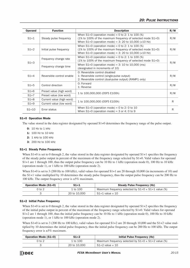
20: PULSE INSTRUCTIONS
S1+0 Operation Mode
The value stored in the data register designated by operand S1+0 determines the frequency range of the pulse output.
0: 10 Hz to 1 kHz
1: 100 Hz to 10 kHz
2: 1 kHz to 100 kHz
3: 200 Hz to 100 kHz
S1+1 Steady Pulse Frequency
When S1+0 is set to 0 through 2, the value stored in the data register designated by operand S1+1 specifies the frequency of the steady pulse output in percent of the maximum of the frequency range selected by S1+0. Valid values for operand S1+1 are 1 through 100, thus the output pulse frequency can be 10 Hz to 1 kHz (operation mode 0), 100 Hz to 10 kHz (operation mode 1), or 1 kHz to 100 kHz (operation mode 2).
When S1+0 is set to 3 (200 Hz to 100 kHz), valid values for operand S1+1 are 20 through 10,000 (in increments of 10) and the S1+1 value multiplied by 10 determines the steady pulse frequency, thus the output pulse frequency can be 200 Hz to 100 kHz. The output frequency error is ±5% maximum.
S1+2 Initial Pulse Frequency
When S1+0 is set to 0 through 2, the value stored in the data register designated by operand S1+2 specifies the frequency of the initial pulse output in percent of the maximum of the frequency range selected by S1+0. Valid values for operand S1+2 are 1 through 100, thus the initial pulse frequency can be 10 Hz to 1 kHz (operation mode 0), 100 Hz to 10 kHz (operation mode 1), or 1 kHz to 100 kHz (operation mode 2).
When S1+0 is set to 3 (200 Hz to 100 kHz), valid values for operand S1+2 are 20 through 10,000 and the S1+2 value mul-tiplied by 10 determines the initial pulse frequency, thus the initial pulse frequency can be 200 Hz to 100 kHz. The output frequency error is ±5% maximum.
S1+1 Steady pulse frequencyWhen S1+0 (operation mode) = 0 to 2: 1 to 100 (%) (1% to 100% of the maximum frequency of selected mode S1+0)When S1+0 (operation mode) = 3: 20 to 10,000 (×10 Hz)
R/W
S1+2 Initial pulse frequencyWhen S1+0 (operation mode) = 0 to 2: 1 to 100 (%) (1% to 100% of the maximum frequency of selected mode S1+0)When S1+0 (operation mode) = 3: 20 to 10,000 (×10 Hz)
R/W
S1+3Frequency change rate
When S1+0 (operation mode) = 0 to 2: 1 to 100 (%) (1% to 100% of the maximum frequency of selected mode S1+0)
R/WFrequency change time
When S1+0 (operation mode) = 3: 10 to 10,000 (ms)(designated in increments of 10)
S1+4 Reversible control enable0: Reversible control disabled 1: Reversible control (single-pulse output) 2: Reversible control (dual-pulse output) (RAMP1 only)
R/W
S1+5 Control direction0: Forward 1: Reverse
R/W
S1+6 Preset value (high word)1 to 100,000,000 (05F5 E100h) R/W
S1+7 Preset value (low word)S1+8 Current value (high word)
1 to 100,000,000 (05F5 E100h) RS1+9 Current value (low word)
S1+10 Error statusWhen S1+0 (operation mode) = 0 to 2: 0 to 10 When S1+0 (operation mode) = 3 or 4: 0 to 9
R
Operation Mode (S1+0) S1+1 Steady Pulse Frequency (Hz)0 to 2 1 to 100 Maximum frequency selected by S1+0 × S1+1 value (%)
3 20 to 10,000 S1+1 value × 10
Operation Mode (S1+0) S1+2 Initial Pulse Frequency (Hz)0 to 2 1 to 100 Maximum frequency selected by S1+0 × S1+2 value (%)
3 20 to 10,000 S1+2 value × 10
Operand Function Description R/W
FC5A MICROSMART USER’S MANUAL 20-15

20: PULSE INSTRUCTIONS
S1+3 Frequency Change Rate / Frequency Change Time
When S1+0 is set to 0 through 2, the value stored in the data register designated by operand S1+3 determines the rate of pulse output frequency change for a period of 10 ms in percent of the maximum of the frequency range selected by S1+0. Valid values for operand S1+3 are 1 through 100, thus the frequency change rate can be 10 Hz to 1 kHz (operation mode 0), 100 Hz to 10 kHz (operation mode 1), or 1 kHz to 100 kHz (operation mode 2).
When S1+0 is set to 3, the value stored in the data register designated by operand S1+3 determines the frequency change time. Valid values are 10 through 10,000 in increments of 10, thus the frequency change time can be 10 to 10,000 ms. The value at the lowest digit is omitted.
The same frequency change rate and frequency change time apply to the accelerating and decelerating periods of the trap-ezoidal frequency change pattern.
S1+4 Reversible Control Enable
The value stored in the data register designated by operand S1+4 specifies one of the output modes.
RAMP1 can designate 0 through 2 for operand S1+4, while RAMP2 can designate 0 and 1.
Operation Mode
Frequency Change Rate / Frequency Change Time
0 to 2 Frequency change rate in 10 ms (Hz) Maximum frequency (Hz) selected by S1+0 × S1+3 value (%)3 Frequency change time (ms) Frequency change time (ms) selected by S1+3
S1+4 Value Reversible Control Description
0Reversible control disabled
Output Q0 or Q2 generates output pulses; used for single-direction control.
Output Q1 can be used for PULS2, PWM2, ZRN2, or an ordinary output.When using RAMP2, output Q3 can be used for an ordinary output.
1Reversible control (Single-pulse output)
Output Q0 or Q2 generates output pulses, and output Q1 or Q3 generates a direction control signal.
Output Q1 or Q3 turns on or off depending on the value stored in data register designated by operand S1+5 (control direction): 0 for forward or 1 for reverse.
2(RAMP1 only)
Reversible control (Dual-pulse output)
Output Q0 generates forward output pulses, and output Q1 generates reverse output pulses.
Output Q0 or Q1 generates output pulses alternately depending on the value stored in data register designated by operand S1+5 (control direction): 0 for forward or 1 for reverse.
Output Pulse
Initial Pulse Frequency
Steady Pulse Frequency
Modes 0 to 2
10 ms
Frequency Change Rate
Mode 3
Frequency Change Time
Output Q0/Q2
Output Q0/Q2
Output Q1/Q3 Forward Reverse
Output Q0
Output Q1
(Forward)
(Reverse)
20-16 FC5A MICROSMART USER’S MANUAL

20: PULSE INSTRUCTIONS
If the value stored in the data register designated by operand S1+4 is changed after the start input for the RAMP instruc-tion has been turned on, the change can take effect only after the CPU starts again.
S1+5 Control Direction
When S1+4 is set to 1 or 2 to enable reversible control, the value stored in the data register designated by operand S1+5 specifies the control direction.
0: Forward
1: Reverse
S1+6 Preset Value (High Word) S1+7 Preset Value (Low Word)
The RAMP1 or RAMP2 instruction generates a predetermined number of output pulses as designated by operands S1+6 and S1+7. The preset value can be 1 through 100,000,000 (05F5 E100h) stored in two consecutive data registers desig-nated by S1+6 (high word) and S1+7 (low word).
S1+8 Current Value (High Word) S1+9 Current Value (Low Word)
While the RAMP1 or RAMP2 instruction is executed to generate output pulses, the output pulse count is stored in two consecutive data registers designated by operands S1+8 (high word) and S1+9 (low word). The current value can be 1 through 100,000,000 (05F5 E100h) and is updated in every scan.
S1+10 Error Status
When the start input for the RAMP instruction is turned on, operand values are checked. When any error is found in the operand values, the data register designated by operand S1+10 stores an error code.
Error Code Description
0 Normal
1Operation mode designation error (S1+0 stores other than 0 through 3)
2Initial pulse frequency designation error Modes 0 to 2: S1+2 stores other than 1 through 100 Mode 3: S1+2 stores other than 20 through 10,000
3Preset value designation error (S1+6 and S1+7 store other than 1 through 100,000,000)
4Steady pulse frequency designation error Modes 0 to 2: S1+1 stores other than 1 through 100 Mode 3: S1+1 stores other than 20 through 10,000
5Frequency change rate designation error Modes 0 to 2: S1+3 stores other than 1 through 100 Mode 3: S1+3 stores other than 10 through 10,000
6 Reversible control enable designation error (S1+4 stores other than 0 through 2)
7 Control direction designation error (S1+5 stores other than 0 and 1)
8
The number of pulses for the frequency change areas calculated from the steady pulse frequency (S1+1), initial pulse frequency (S1+2), and frequency change rate/time (S1+3) exceeds the preset value (S1+6/7) of the total output pulses. To correct this error, reduce the value of the steady pulse frequency (S1+1) or initial pulse frequency (S1+2), or increase the frequency change rate/time (S1+3).
9The initial pulse frequency (S1+2) is equal to or larger than the steady pulse frequency (S1+1). Reduce the initial pulse frequency (S1+2) to a value smaller than the steady pulse frequency (S1+1).
10
Modes 0 to 2:The frequency change rate (S1+3) is larger than the difference between the initial pulse frequency (S1+2) and the steady pulse frequency (S1+1). Reduce the frequency change rate (S1+3) or the initial pulse fre-quency (S1+2).
FC5A MICROSMART USER’S MANUAL 20-17

20: PULSE INSTRUCTIONS
Destination Operand D1 (Status Relay)Four internal relays starting with the operand designated by D1 indicate the status of the RAMP instruction. These oper-ands are for read only.
D1+0 Pulse Output ON
The internal relay designated by operand D1+0 remains on while the RAMP instruction generates output pulses. When the start input for the RAMP instruction is turned off or when the RAMP instruction has completed generating a predeter-mined number of output pulses, the internal relay designated by operand D1+0 turns off.
D1+1 Pulse Output Complete
The internal relay designated by operand D1+1 turns on when the RAMP instruction has completed generating a predeter-mined number of output pulses or when the RAMP instruction is stopped to generate output pulses. When the start input for the RAMP instruction is turned on, the internal relay designated by operand D1+1 turns off.
D1+2 Pulse Output Status
The internal relay designated by operand D1+2 turns on while the output pulse frequency is increasing or decreasing, and turns off when the output pulse frequency reaches the steady pulse frequency (S1+1). While the pulse output is off, the internal relay designated by operand D1+2 remains off.
D1+3 Pulse Output Overflow
The internal relay designated by operand D1+3 turns on when the RAMP instruction has generated more than the prede-termined number of output pulses (S1+6/7). When an overflow occurs, the current value (S1+8/9) stops at the preset value (S1+6/7). When the start input for the RAMP instruction is turned on, the internal relay designated by operand D1+3 turns off.
Special Data Registers for Pulse OutputsThree additional special data registers store the current frequency of pulse outputs.
Operand Function Description R/W
D1+0 Pulse output ON0: Pulse output OFF 1: Pulse output ON
R
D1+1 Pulse output complete0: Pulse output not complete 1: Pulse output complete
R
D1+2 Pulse output status0: Steady pulse output 1: Changing output pulse frequency
R
D1+3 Pulse output overflow0: Overflow not occurred 1: Overflow occurred
R
Allocation No. Function Description
D8055Current Pulse Frequency of PULS1 or RAMP1 (Q0)
While the PULS1 or RAMP1 instruction is executed, D8055 stores the cur-rent pulse frequency of output Q0. The value is updated every scan.
D8056Current Pulse Frequency of PULS2 or RAMP1 (Q1)
While the PULS2 or RAMP1 (reversible control dual-pulse output) instruc-tion is executed, D8056 stores the current pulse frequency of output Q1. The value is updated every scan.
D8059Current Pulse Frequency of PULS3 or RAMP2 (Q2)
While the PULS3 or RAMP2 instruction is executed, D8059 stores the cur-rent pulse frequency of output Q2. The value is updated every scan.
20-18 FC5A MICROSMART USER’S MANUAL
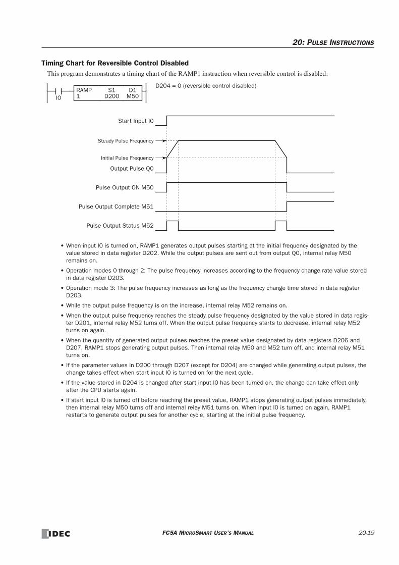
20: PULSE INSTRUCTIONS
Timing Chart for Reversible Control DisabledThis program demonstrates a timing chart of the RAMP1 instruction when reversible control is disabled.
D1M50I0
RAMP1
S1D200
D204 = 0 (reversible control disabled)
• When input I0 is turned on, RAMP1 generates output pulses starting at the initial frequency designated by the value stored in data register D202. While the output pulses are sent out from output Q0, internal relay M50 remains on.
• Operation modes 0 through 2: The pulse frequency increases according to the frequency change rate value stored in data register D203.
• Operation mode 3: The pulse frequency increases as long as the frequency change time stored in data register D203.
• While the output pulse frequency is on the increase, internal relay M52 remains on.
• When the output pulse frequency reaches the steady pulse frequency designated by the value stored in data regis-ter D201, internal relay M52 turns off. When the output pulse frequency starts to decrease, internal relay M52 turns on again.
• When the quantity of generated output pulses reaches the preset value designated by data registers D206 and D207, RAMP1 stops generating output pulses. Then internal relay M50 and M52 turn off, and internal relay M51 turns on.
• If the parameter values in D200 through D207 (except for D204) are changed while generating output pulses, the change takes effect when start input I0 is turned on for the next cycle.
• If the value stored in D204 is changed after start input I0 has been turned on, the change can take effect only after the CPU starts again.
• If start input I0 is turned off before reaching the preset value, RAMP1 stops generating output pulses immediately, then internal relay M50 turns off and internal relay M51 turns on. When input I0 is turned on again, RAMP1 restarts to generate output pulses for another cycle, starting at the initial pulse frequency.
Pulse Output Status M52
Output Pulse Q0
Start Input I0
Pulse Output ON M50
Pulse Output Complete M51
Initial Pulse Frequency
Steady Pulse Frequency
FC5A MICROSMART USER’S MANUAL 20-19

20: PULSE INSTRUCTIONS
Timing Chart for Reversible Control with Single Pulse OutputThis program demonstrates a timing chart of the RAMP1 instruction when reversible control is enabled with single pulse output.
D1M50I0
RAMP1
S1D200
D204 = 1 (reversible control with single pulse output)
• When input I0 is turned on, RAMP1 generates output pulses starting at the initial frequency designated by the value stored in data register D202. While the output pulses are sent out from output Q0, internal relay M50 remains on.
• Operation modes 0 through 2: The pulse frequency increases according to the frequency change rate value stored in data register D203.
• Operation mode 3: The pulse frequency increases as long as the frequency change time stored in data register D203.
• While the output pulse frequency is on the increase, internal relay M52 remains on.
• Depending on the control direction designated by the value stored in data register D205, control direction output Q1 turns off or on while D205 stores 0 (forward) or 1 (reverse), respectively.
• When the output pulse frequency reaches the steady pulse frequency designated by the value stored in data regis-ter D201, internal relay M52 turns off. When the output pulse frequency starts to decrease, internal relay M52 turns on again.
• When the quantity of generated output pulses reaches the preset value designated by data registers D206 and D207, RAMP1 stops generating output pulses. Then internal relay M50 and M52 turn off, and internal relay M51 turns on.
• If the parameter values in D200 through D207 (except for D204) are changed while generating output pulses, the change takes effect when start input I0 is turned on for the next cycle.
• If the value stored in D204 is changed after start input I0 has been turned on, the change can take effect only after the CPU starts again.
• If start input I0 is turned off before reaching the preset value, RAMP1 stops generating output pulses immediately, then internal relay M50 turns off and internal relay M51 turns on. When input I0 is turned on again, RAMP1 restarts to generate output pulses for another cycle, starting at the initial pulse frequency.
Pulse Output Status M52
Output Pulse Q0
Start Input I0
Control Direction Output Q1
Pulse Output Complete M51
Initial Pulse Frequency
Steady Pulse Frequency
Control Direction D205 0 (Forward) 1 (Reverse)
Pulse Output ON M50
20-20 FC5A MICROSMART USER’S MANUAL

20: PULSE INSTRUCTIONS
Timing Chart for Reversible Control with Dual Pulse OutputThis program demonstrates a timing chart of the RAMP1 instruction when reversible control is enabled with dual pulse output.
D1M50I0
RAMP1
S1D200
D204 = 2 (reversible control with dual pulse output)
• When input I0 is turned on, RAMP1 generates output pulses starting at the initial frequency designated by the value stored in data register D202. While the output pulses are sent out from output Q0 or Q1, internal relay M50 remains on.
• Operation modes 0 through 2: The pulse frequency increases according to the frequency change rate value stored in data register D203.
• Operation mode 3: The pulse frequency increases as long as the frequency change time stored in data register D203.
• While the output pulse frequency is on the increase, internal relay M52 remains on.
• Depending on the control direction designated by the value stored in data register D205, output Q0 or Q1 sends out output pulses while D205 stores 0 (forward) or 1 (reverse), respectively.
• When the output pulse frequency reaches the steady pulse frequency designated by the value stored in data regis-ter D201, internal relay M52 turns off. When the output pulse frequency starts to decrease, internal relay M52 turns on again.
• When the quantity of generated output pulses reaches the preset value designated by data registers D206 and D207, RAMP1 stops generating output pulses. Then internal relay M50 and M52 turn off, and internal relay M51 turns on.
• If the parameter values in D200 through D207 (except for D204) are changed while generating output pulses, the change takes effect when start input I0 is turned on for the next cycle.
• If the value stored in D204 is changed after start input I0 has been turned on, the change can take effect only after the CPU starts again.
• If start input I0 is turned off before reaching the preset value, RAMP1 stops generating output pulses immediately, then internal relay M50 turns off and internal relay M51 turns on. When input I0 is turned on again, RAMP1 restarts to generate output pulses for another cycle, starting at the initial pulse frequency.
Forward (CW) Output Pulse Q0
Start Input I0
Initial Pulse Frequency
Steady Pulse Frequency
Control Direction D205 0 (Forward) 1 (Reverse)
Pulse Output Status M52
Pulse Output Complete M51
Pulse Output ON M50
Reverse (CCW) Output Pulse Q1
Initial Pulse Frequency
Steady Pulse Frequency
FC5A MICROSMART USER’S MANUAL 20-21

20: PULSE INSTRUCTIONS
Sample Program: RAMP1 — Reversible Control DisabledThis program demonstrates a user program of the RAMP1 instruction to generate 48,000 pulses from output Q0.
Steady pulse frequency: 6 kHz
Initial pulse frequency: 300 Hz
Frequency change time: 2,000 ms
Reversible control enable: Reversible control disabled
Preset value: 48,000 pulses total
Programming WindLDR
On the WindLDR editing screen, place the cursor where you want to insert the pulse instruction macro, and type RAMPST. Enter parameters as shown below.
Operand SettingsOperand Function Description Allocation No. (Value)
S1+0 Operation mode Frequency range 200 Hz to 100 kHz D0 (3)S1+1 Steady pulse frequency 6 kHz D1 (600)S1+2 Initial pulse frequency 300 Hz D2 (30)S1+3 Frequency change time 2,000 ms D3 (2000)S1+4 Reversible control enable Reversible control disabled D4 (0)S1+5 Control direction Not used (no effect) D5S1+6 Preset value (high word)
48,000 D6/D7 (48000)S1+7 Preset value (low word)S1+8 Current value (high word)
0 to 48,000 D8/D9S1+9 Current value (low word)S1+10 Error status D10
D1+0 Pulse output ON0: Pulse output OFF 1: Pulse output ON
M100
D1+1 Pulse output complete0: Pulse output not complete 1: Pulse output complete
M101
D1+2 Pulse output status0: Steady pulse output 1: Changing output pulse frequency
M102
D1+3 Pulse output overflow0: Overflow not occurred 1: Overflow occurred
M103
Same operand as S1 for the RAMP1
instruction
M8120
M8120 is the initialize pulse special internal relay.
When the CPU starts, RAMPST macro designates parameters for pulse output.
When start input I0 is turned on, RAMP1 starts to generate 48,000 output pulses.I0
D1M100
RAMP1
S1D0
S1D0
RAMPST
20-22 FC5A MICROSMART USER’S MANUAL
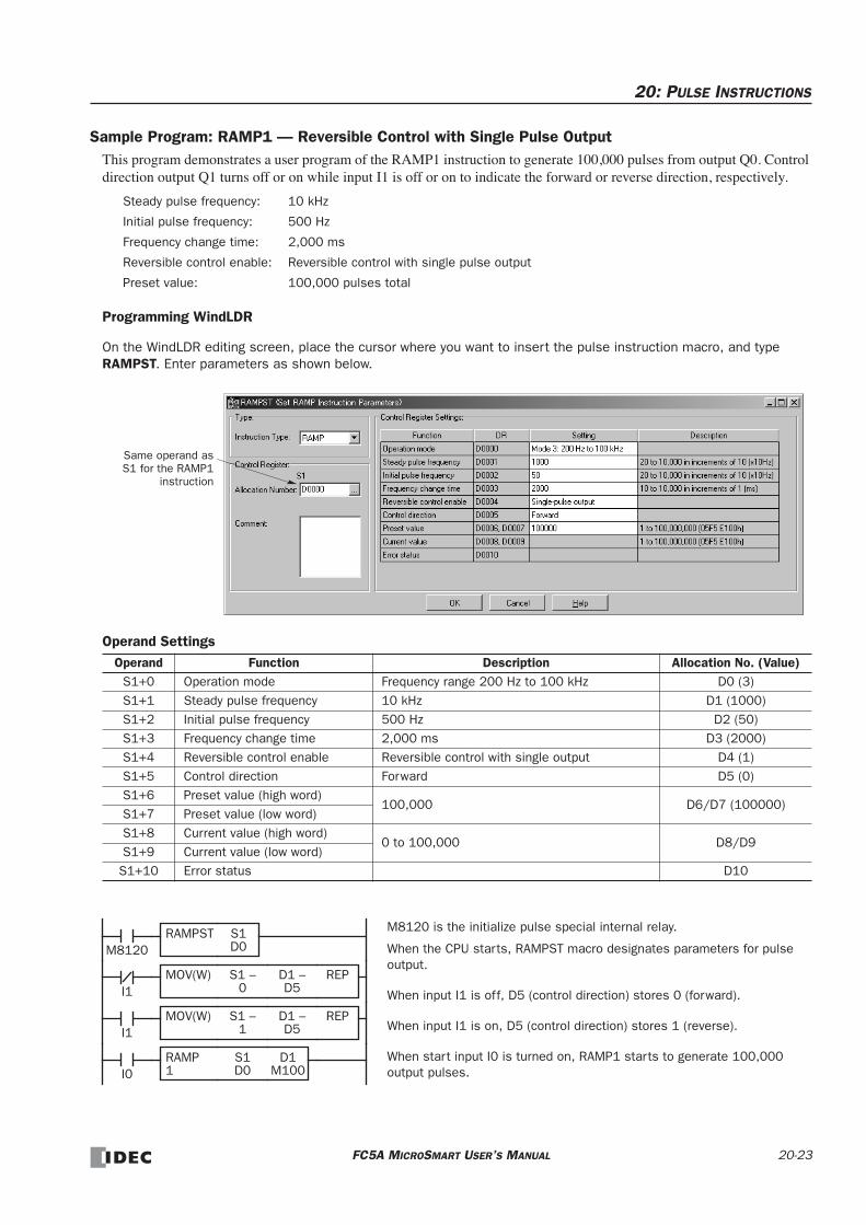
20: PULSE INSTRUCTIONS
Sample Program: RAMP1 — Reversible Control with Single Pulse OutputThis program demonstrates a user program of the RAMP1 instruction to generate 100,000 pulses from output Q0. Control direction output Q1 turns off or on while input I1 is off or on to indicate the forward or reverse direction, respectively.
Steady pulse frequency: 10 kHz
Initial pulse frequency: 500 Hz
Frequency change time: 2,000 ms
Reversible control enable: Reversible control with single pulse output
Preset value: 100,000 pulses total
Programming WindLDR
On the WindLDR editing screen, place the cursor where you want to insert the pulse instruction macro, and type RAMPST. Enter parameters as shown below.
Operand SettingsOperand Function Description Allocation No. (Value)
S1+0 Operation mode Frequency range 200 Hz to 100 kHz D0 (3)S1+1 Steady pulse frequency 10 kHz D1 (1000)S1+2 Initial pulse frequency 500 Hz D2 (50)S1+3 Frequency change time 2,000 ms D3 (2000)S1+4 Reversible control enable Reversible control with single output D4 (1)S1+5 Control direction Forward D5 (0)S1+6 Preset value (high word)
100,000 D6/D7 (100000)S1+7 Preset value (low word)S1+8 Current value (high word)
0 to 100,000 D8/D9S1+9 Current value (low word)S1+10 Error status D10
Same operand as S1 for the RAMP1
instruction
M8120
M8120 is the initialize pulse special internal relay.
When the CPU starts, RAMPST macro designates parameters for pulse output.
When input I1 is off, D5 (control direction) stores 0 (forward).
When input I1 is on, D5 (control direction) stores 1 (reverse).
When start input I0 is turned on, RAMP1 starts to generate 100,000 output pulses.I0
D1M100
RAMP1
S1D0
REPS1 –0
MOV(W) D1 –D5
REPS1 –1
MOV(W) D1 –D5I1
I1
S1D0
RAMPST
FC5A MICROSMART USER’S MANUAL 20-23

20: PULSE INSTRUCTIONS
Sample Program: RAMP1 — Reversible Control with Dual Pulse OutputThis program demonstrates a user program of the RAMP1 instruction to generate 1,000,000 pulses from output Q0 (for-ward pulse) or Q1 (reverse pulse) while input I1 is off or on, respectively.
Steady pulse frequency: 30 kHz
Initial pulse frequency: 10 kHz
Frequency change time: 2,000 ms
Reversible control enable: Reversible control with dual pulse output
Preset value: 1,000,000 pulses total
Programming WindLDR
On the WindLDR editing screen, place the cursor where you want to insert the pulse instruction macro, and type RAMPST. Enter parameters as shown below.
Operand SettingsOperand Function Description Allocation No. (Value)
S1+0 Operation mode Frequency range 1 kHz to 100 kHz D0 (2)S1+1 Steady pulse frequency 30 kHz D1 (30)S1+2 Initial pulse frequency 10 kHz D2 (10)S1+3 Frequency change time 2,000 ms D3 (2000)S1+4 Reversible control enable Reversible control with dual output D4 (2)S1+5 Control direction Forward D5 (0)S1+6 Preset value (high word)
1,000,000 D6/D7 (1000000)S1+7 Preset value (low word)S1+8 Current value (high word)
0 to 1,000,000 D8/D9S1+9 Current value (low word)S1+10 Error status D10
Same operand as S1 for the RAMP1
instruction
M8120
M8120 is the initialize pulse special internal relay.
When the CPU starts, RAMPST macro designates parameters for pulse output.
When input I1 is off, D5 (control direction) stores 0 (forward).
When input I1 is on, D5 (control direction) stores 1 (reverse).
When start input I0 is turned on, RAMP1 starts to generate 1,000,000 output pulses.I0
D1M100
RAMP1
S1D0
REPS1 –0
MOV(W) D1 –D5
REPS1 –1
MOV(W) D1 –D5I1
I1
S1D0
RAMPST
20-24 FC5A MICROSMART USER’S MANUAL

20: PULSE INSTRUCTIONS
ZRN1 (Zero Return 1)
ZRN2 (Zero Return 2)
ZRN3 (Zero Return 3)
Note: The ZRN1, ZRN2, and ZRN3 instructions can be used only once in a user program. When ZRN1, ZRN2, or ZRN3 is not used, unused output Q0, Q1, or Q2 can be used for another pulse instruction or ordinary output.
Applicable CPU Modules
Valid Operands
Source operand S1 (control register) uses 5 data registers starting with the operand designated as S1. Data registers D0-D1995, D2000-D7995, and D10000-D49995 can be designated as S1. For details, see the following pages.
Source operand S2 (deceleration input) can designate inputs I0 to I627 and internal relays M0 to M2557. Special internal relays cannot be designated as S2.
Destination operand D1 (status relay) uses 2 internal relays starting with the operand designated as D1. Internal relays M0 to M2550 can be designated as D1. The least significant digit of the internal relay number designated as D1 must be 0, oth-erwise the ZRN instruction does not operate correctly. Special internal relays cannot be designated as D1. For details, see page 6-2.
FC5A-C10R2/C FC5A-C16R2/C FC5A-C24R2/C FC5A-D16RK1/RS1 FC5A-D32K3/S3
— — — X (ZRN1 and ZRN2) X
Operand Function I Q M R T C D Constant Repeat
S1 (Source 1) Control register — — — — — — X — —
S2 (Source 2) Deceleration input X — — — — — — —
D1 (Destination 1) Status relay — — — — — — — —
When input is on, the ZRN1 instruction sends out a pulse output of a predetermined high frequency from output Q0. When a deceleration input turns on, the output frequency decreases to a creep frequency. When the deceleration input turns off, the ZRN1 instruction stops gener-ating output pulses.
The output pulse width ratio is fixed at 50%.
ZRN1
S1*****
D1*****
S2*****
When input is on, the ZRN2 instruction sends out a pulse output of a predetermined high frequency from output Q1. When a deceleration input turns on, the output frequency decreases to a creep frequency. When the deceleration input turns off, the ZRN2 instruction stops gener-ating output pulses.
The output pulse width ratio is fixed at 50%.
ZRN2
S1*****
D1*****
S2*****
When input is on, the ZRN3 instruction sends out a pulse output of a predetermined high frequency from output Q2. When a deceleration input turns on, the output frequency decreases to a creep frequency. When the deceleration input turns off, the ZRN3 instruction stops gener-ating output pulses.
The output pulse width ratio is fixed at 50%.
ZRN3
S1*****
D1*****
S2*****
Not available on FC5A-16RK1/RS1
FC5A MICROSMART USER’S MANUAL 20-25

20: PULSE INSTRUCTIONS
Source Operand S1 (Control Register)Store appropriate values to data registers starting with the operand designated by S1 before executing the ZRN instruction as required, and make sure that the values are within the valid range. Operand S1+4 is for read only.
S1+0 Initial Operation Mode
The value stored in the data register designated by operand S1+0 determines the frequency range of the high-frequency initial pulse output.
0: 10 Hz to 1 kHz
1: 100 Hz to 10 kHz
2: 1 kHz to 100 kHz
3: 200 Hz to 100 kHz
S1+1 Initial Pulse Frequency
When S1+0 is set to 0 through 2, the value stored in the data register designated by operand S1+1 specifies the initial fre-quency of the pulse output in percent of the maximum of the frequency range selected by S1+0. Valid values for operand S1+1 are 1 through 100, thus the initial pulse frequency can be 10 Hz to 1 kHz (operation mode 0), 100 Hz to 10 kHz (operation mode 1), or 1 kHz to 100 kHz (operation mode 2).
When S1+0 is set to 3 (200 Hz to 100 kHz), valid values for operand S1+1 are 20 through 10,000 and the S1+1 value mul-tiplied by 10 determines the output pulse frequency, thus the output pulse frequency can be 200 Hz to 100 kHz. The pulse frequency error is ±5% maximum.
S1+2 Creep Operation Mode
The value stored in the data register designated by operand S1+2 determines the frequency range of the low-frequency creep pulse output.
0: 10 Hz to 1 kHz
1: 100 Hz to 10 kHz
2: 1 kHz to 100 kHz
3: 200 Hz to 100 kHz
Operand Function Description R/W
S1+0 Initial operation mode
0: 10 Hz to 1 kHz 1: 100 Hz to 10 kHz 2: 1 kHz to 100 kHz 3: 200 Hz to 100 kHz
R/W
S1+1 Initial pulse frequencyWhen S1+0 (operation mode) = 0 to 2: 1 to 100 (%) (1% to 100% of the maximum frequency of selected mode S1+0)When S1+0 (operation mode) = 3: 20 to 10,000 (×10 Hz)
R/W
S1+2 Creep operation mode
0: 10 Hz to 1 kHz 1: 100 Hz to 10 kHz 2: 1 kHz to 100 kHz 3: 200 Hz to 100 kHz
R/W
S1+3 Creep pulse frequencyWhen S1+2 (operation mode) = 0 to 2: 1 to 100 (%) (1% to 100% of the maximum frequency of selected mode S1+2)When S1+2 (operation mode) = 3: 20 to 10,000 (×10 Hz)
R/W
S1+4 Error status 0 to 2 R
Initial Operation Mode (S1+0) S1+1 Initial Pulse Frequency (Hz)
0 to 2 1 to 100 Maximum frequency selected by S1+0 × S1+1 value (%)
3 20 to 10,000 S1+1 value × 10
20-26 FC5A MICROSMART USER’S MANUAL
20: PULSE INSTRUCTIONS
S1+3 Creep Pulse Frequency
When S1+2 is set to 0 through 2, the value stored in the data register designated by operand S1+3 specifies the frequency of the creep pulse output in percent of the maximum of the frequency range selected by S1+2. Valid values for operand S1+3 are 1 through 100, thus the initial pulse frequency can be 10 Hz to 1 kHz (operation mode 0), 100 Hz to 10 kHz (operation mode 1), or 1 kHz to 100 kHz (operation mode 2).
When S1+2 is set to 3 (200 Hz to 100 kHz), valid values for operand S1+3 are 20 through 10,000 and the S1+3 value mul-tiplied by 10 determines the creep pulse frequency, thus the creep pulse frequency can be 200 Hz to 100 kHz. The pulse frequency error is ±5% maximum.
S1+4 Error Status
When the start input for the ZRN instruction is turned on, operand values are checked. When any error is found in the operand values, the data register designated by operand S1+4 stores an error code.
Source Operand S2 (Deceleration Input)When the deceleration input turns on while the ZRN instruction is generating output pulses of the initial pulse frequency, the pulse frequency is changed to the creep pulse frequency. When the deceleration input turns off, the ZRN instruction stops generating output pulses.
When using the ZRN1, ZRN2, and ZRN3 instructions, designate different input or internal relay numbers as deceleration inputs for the ZRN1, ZRN2, and ZRN3 instructions. If the same deceleration input is used and the ZRN1, ZRN2, and ZRN3 instructions are executed at the same time, the pulse outputs may not turn off when the deceleration input turns on.
The deceleration input is available in two types depending on the designated operand number.
High-speed Deceleration Input (I2, I3, I4, I5)
The high-speed deceleration input uses interrupt processing to read the deceleration input signal immediately without regard to the scan time.
When I2 through I5 are used as a deceleration input for the ZRN instruction, designate these input numbers as normal inputs in the Function Area Settings. If I2 through I5 used as a deceleration input are designated as an interrupt input, catch input, or high-speed counter input in the Function Area Settings, the inputs work as a deceleration input for the ZRN instruction; the designation in the Function Area Settings will have no effect.
When using a high-speed deceleration input, make sure that the input contact does not bounce. If the input signal contains chatter, the pulse output will be stopped immediately.
Normal Deceleration Input (I0, I1, I6 through I627, M0 through M2557)
The normal deceleration input reads the deceleration input signal when the input data is updated at the END processing, so the timing of accepting the deceleration input depends on the scan time.
Creep Operation Mode (S1+2) S1+3 Creep Pulse Frequency (Hz)
0 to 2 1 to 100 Maximum frequency selected by S1+2 × S1+3 value (%)
3 20 to 10,000 S1+3 value × 10
Error Code Description
0 Normal
1 Operation mode designation error (S1+0 or S1+2 stores other than 0 through 3)
2Output pulse frequency designation errorModes 0 to 2: S1+1 or S1+3 stores other than 1 through 100 Mode 3: S1+1 or S1+3 stores other than 20 through 10,000
Operand Function Description
S2High-speed deceleration input I2, I3, I4, I5Normal deceleration input I0, I1, I6 through I627, M0 through M2557
FC5A MICROSMART USER’S MANUAL 20-27
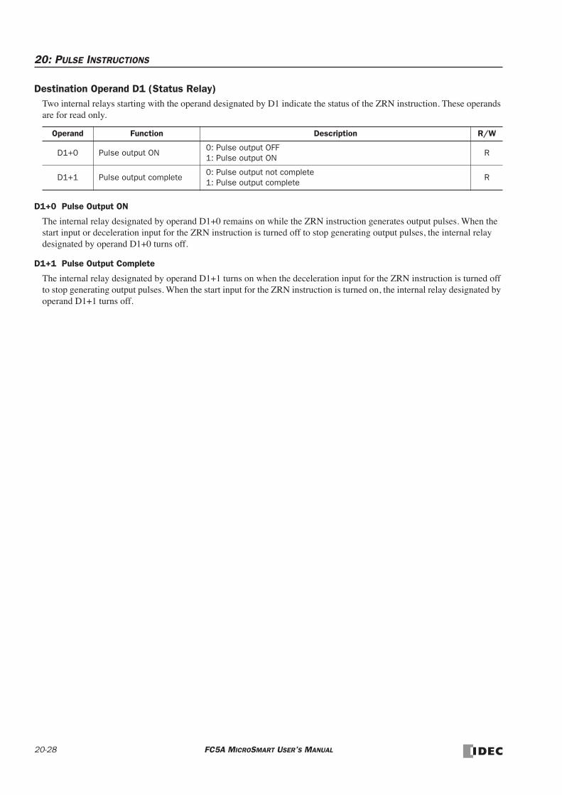
20: PULSE INSTRUCTIONS
Destination Operand D1 (Status Relay)Two internal relays starting with the operand designated by D1 indicate the status of the ZRN instruction. These operands are for read only.
D1+0 Pulse Output ON
The internal relay designated by operand D1+0 remains on while the ZRN instruction generates output pulses. When the start input or deceleration input for the ZRN instruction is turned off to stop generating output pulses, the internal relay designated by operand D1+0 turns off.
D1+1 Pulse Output Complete
The internal relay designated by operand D1+1 turns on when the deceleration input for the ZRN instruction is turned off to stop generating output pulses. When the start input for the ZRN instruction is turned on, the internal relay designated by operand D1+1 turns off.
Operand Function Description R/W
D1+0 Pulse output ON0: Pulse output OFF 1: Pulse output ON
R
D1+1 Pulse output complete0: Pulse output not complete 1: Pulse output complete
R
20-28 FC5A MICROSMART USER’S MANUAL
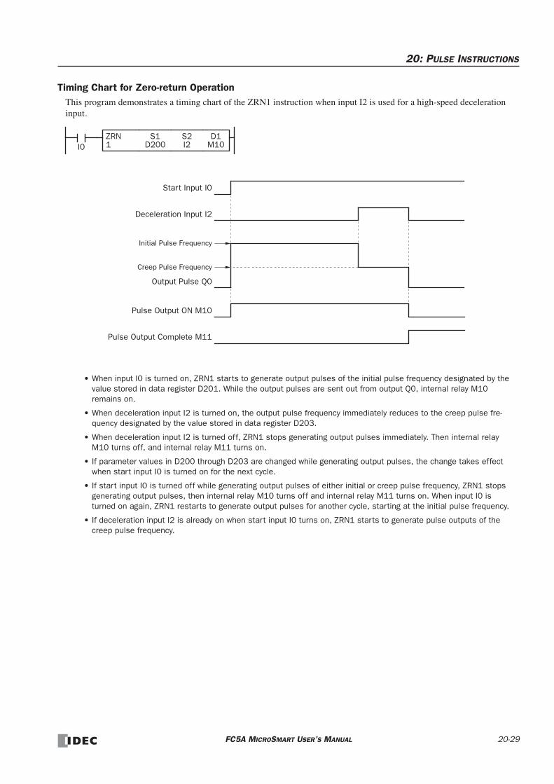
20: PULSE INSTRUCTIONS
Timing Chart for Zero-return OperationThis program demonstrates a timing chart of the ZRN1 instruction when input I2 is used for a high-speed deceleration input.
D1M10I0
ZRN1
S1D200
Output Pulse Q0
Deceleration Input I2
Start Input I0
• When input I0 is turned on, ZRN1 starts to generate output pulses of the initial pulse frequency designated by the value stored in data register D201. While the output pulses are sent out from output Q0, internal relay M10 remains on.
• When deceleration input I2 is turned on, the output pulse frequency immediately reduces to the creep pulse fre-quency designated by the value stored in data register D203.
• When deceleration input I2 is turned off, ZRN1 stops generating output pulses immediately. Then internal relay M10 turns off, and internal relay M11 turns on.
• If parameter values in D200 through D203 are changed while generating output pulses, the change takes effect when start input I0 is turned on for the next cycle.
• If start input I0 is turned off while generating output pulses of either initial or creep pulse frequency, ZRN1 stops generating output pulses, then internal relay M10 turns off and internal relay M11 turns on. When input I0 is turned on again, ZRN1 restarts to generate output pulses for another cycle, starting at the initial pulse frequency.
• If deceleration input I2 is already on when start input I0 turns on, ZRN1 starts to generate pulse outputs of the creep pulse frequency.
Pulse Output ON M10
Pulse Output Complete M11
S2I2
Initial Pulse Frequency
Creep Pulse Frequency
FC5A MICROSMART USER’S MANUAL 20-29

20: PULSE INSTRUCTIONS
Sample Program: ZRN1This program demonstrates a user program of the ZRN1 instruction used for zero-return operation to generate output pulses of 3 kHz initial pulse frequency from output Q0 while input I1 is on. When deceleration input I3 is turned on, the output pulse frequency reduces to the creep pulse frequency of 800 Hz. When deceleration input I3 is turned off, ZRN1 stops generating output pulses.
Initial pulse frequency: 3 kHz
Creep pulse frequency: 800 Hz
Deceleration input: I3 (high-speed deceleration input)
Programming WindLDR
On the WindLDR editing screen, place the cursor where you want to insert the pulse instruction macro, and type ZRNST. Enter parameters as shown below.
Operand SettingsOperand Function Description Allocation No. (Value)
S1+0 Initial operation mode Frequency range 100 Hz to 10 kHz D0 (1)S1+1 Initial pulse frequency 10 kHz × 30% = 3 kHz D1 (30)S1+2 Creep operation mode Frequency range 10 Hz to 1 kHz D2 (0)S1+3 Creep pulse frequency 1 kHz × 80% = 800 Hz D3 (80)S1+4 Error status D4S2 Deceleration input High-speed deceleration input I3
D1+0 Pulse output ON0: Pulse output OFF 1: Pulse output ON
M100
D1+1 Pulse output complete0: Pulse output not complete 1: Pulse output complete
M101
Same operand as S1 for the ZRN1
instruction
M8120
M8120 is the initialize pulse special internal relay.
When the CPU starts, ZRNST macro designates parameters for pulse out-put.
Pulse output ON flag M100 is turned off.
Pulse output complete flag M101 is turned off.
When start input I1 is turned on, ZRN1 starts to generate output pulses from output Q0.I1
D1M100
ZRN1
S1D0
M100R
M101R
S2I3
S1D0
ZRNST
20-30 FC5A MICROSMART USER’S MANUAL

21: PID INSTRUCTION
IntroductionThe PID instruction implements a PID (proportional, integral, and derivative) algorithm with built-in auto tuning to deter-mine PID parameters, such as proportional gain, integral time, derivative time, and control action automatically. In addi-tion, advanced auto tuning automatically determines the PID parameters without the need for designating auto tuning parameters.
The PID instruction is primarily designed for use with an analog I/O module to read analog input data, and turns on and off a designated output to perform PID control in applications such as temperature control described in the application exam-ple on page 21-18. In addition, the PID instruction also generates an output manipulated variable for analog output mod-ule. When this operand value is moved to an analog output module, a voltage (0 to 10V DC) or current (4 to 20 mA DC) output can be generated.
PID (PID Control)
Applicable CPU Modules and Quantity of PID InstructionsA maximum of 32 or 56 PID instructions can be used in a user program, depending on the CPU module type.
• Special technical knowledge about the PID control is required to use the PID function of the Micro-Smart. Use of the PID function without understanding the PID control may cause the MicroSmart to perform unexpected operation, resulting in disorder of the control system, damage, or accidents.
• When using the PID instruction for feedback control, emergency stop and interlocking circuits must be configured outside the MicroSmart. If such a circuit is configured inside the MicroSmart, failure of inputting the process variable may cause equipment damage or accidents.
FC5A-C10R2/C FC5A-C16R2/C FC5A-C24R2/C FC5A-D16RK1/RS1 FC5A-D32K3/S3
— — X (32) X (56) X (56)
Warning
When input is on, auto tuning and/or PID action is exe-cuted according to the value (0 through 4) stored in a data register operand assigned for operation mode.
D1*****
S1*****
PID(*)0-****
S2*****
S3*****
S4*****
FC5A MICROSMART USER’S MANUAL 21-1
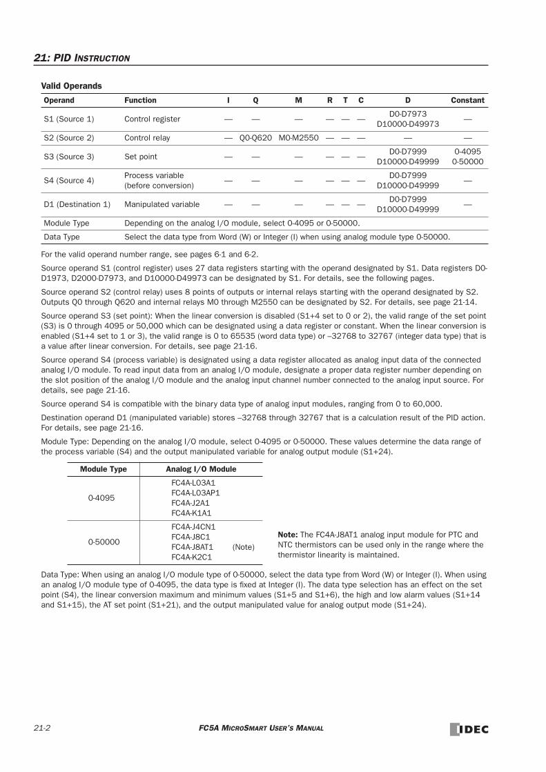
21: PID INSTRUCTION
Valid Operands
For the valid operand number range, see pages 6-1 and 6-2.
Source operand S1 (control register) uses 27 data registers starting with the operand designated by S1. Data registers D0-D1973, D2000-D7973, and D10000-D49973 can be designated by S1. For details, see the following pages.
Source operand S2 (control relay) uses 8 points of outputs or internal relays starting with the operand designated by S2. Outputs Q0 through Q620 and internal relays M0 through M2550 can be designated by S2. For details, see page 21-14.
Source operand S3 (set point): When the linear conversion is disabled (S1+4 set to 0 or 2), the valid range of the set point (S3) is 0 through 4095 or 50,000 which can be designated using a data register or constant. When the linear conversion is enabled (S1+4 set to 1 or 3), the valid range is 0 to 65535 (word data type) or –32768 to 32767 (integer data type) that is a value after linear conversion. For details, see page 21-16.
Source operand S4 (process variable) is designated using a data register allocated as analog input data of the connected analog I/O module. To read input data from an analog I/O module, designate a proper data register number depending on the slot position of the analog I/O module and the analog input channel number connected to the analog input source. For details, see page 21-16.
Source operand S4 is compatible with the binary data type of analog input modules, ranging from 0 to 60,000.
Destination operand D1 (manipulated variable) stores –32768 through 32767 that is a calculation result of the PID action. For details, see page 21-16.
Module Type: Depending on the analog I/O module, select 0-4095 or 0-50000. These values determine the data range of the process variable (S4) and the output manipulated variable for analog output module (S1+24).
Data Type: When using an analog I/O module type of 0-50000, select the data type from Word (W) or Integer (I). When using an analog I/O module type of 0-4095, the data type is fixed at Integer (I). The data type selection has an effect on the set point (S4), the linear conversion maximum and minimum values (S1+5 and S1+6), the high and low alarm values (S1+14 and S1+15), the AT set point (S1+21), and the output manipulated value for analog output mode (S1+24).
Operand Function I Q M R T C D Constant
S1 (Source 1) Control register — — — — — —D0-D7973
D10000-D49973—
S2 (Source 2) Control relay — Q0-Q620 M0-M2550 — — — — —
S3 (Source 3) Set point — — — — — —D0-D7999
D10000-D499990-40950-50000
S4 (Source 4)Process variable (before conversion)
— — — — — —D0-D7999
D10000-D49999—
D1 (Destination 1) Manipulated variable — — — — — —D0-D7999
D10000-D49999—
Module Type Depending on the analog I/O module, select 0-4095 or 0-50000.
Data Type Select the data type from Word (W) or Integer (I) when using analog module type 0-50000.
Module Type Analog I/O Module
0-4095
FC4A-L03A1 FC4A-L03AP1 FC4A-J2A1 FC4A-K1A1
0-50000
FC4A-J4CN1 FC4A-J8C1 FC4A-J8AT1 (Note) FC4A-K2C1
Note: The FC4A-J8AT1 analog input module for PTC and NTC thermistors can be used only in the range where the thermistor linearity is maintained.
21-2 FC5A MICROSMART USER’S MANUAL

21: PID INSTRUCTION
Source Operand S1 (Control Register)Store appropriate values to data registers starting with the operand designated by S1 before executing the PID instruction as required, and make sure that the values are within the valid range. Operands S1+0 through S1+2, S1+23, and S1+24 are for read only. For programming the operands using a macro, see page 21-21.
Operand Function Description R/W
S1+0Process variable (after conversion)
When S1+4 (control mode) = 1 or 3 (enable linear conversion): Stores the process variable after conversion.When S1+4 (control mode) = 0 or 2 (disable linear conversion): Stores the process variable without conversion.
R
S1+1 Output manipulated variableStores the output manipulated variable (manual mode output variable and AT output manipulated variable) in percent. 0 to 100 (0% to 100%)
R
S1+2 Operating status Stores the operating or error status of the PID instruction. R
S1+3 Operation mode
0: PID action 1: AT (auto tuning) + PID action 2: AT (auto tuning) 3: Advanced AT + PID action 4: Advanced AT
R/W
S1+4Control mode (linear conversion and proportional term)
0: Disable linear conversion, proportional gain 1: Enable linear conversion, proportional gain 2: Disable linear conversion, proportional band 3: Enable linear conversion, proportional band
R/W
S1+5Linear conversion maximum value
Word data type: 0 to 65535 Integer data type: –32768 to +32767
R/W
S1+6Linear conversion minimum value
Word data type: 0 to 65535 Integer data type: –32768 to +32767
R/W
S1+7 Proportional term
When S1+4 (control mode) = 0 or 1 (proportional gain):1 to 10000 (0.01% to 100.00%) 0 designates 0.01%, ≥10001 designates 100.00%
When S1+4 (control mode) = 2 or 3 (proportional band):1 to 10000 (±0.01% to ±100.00%) 0 designates ±0.01%, ≥10001 designates ±100.00%
R/W
S1+8 Integral time 1 to 65535 (0.1 sec to 6553.5 sec), 0 disables integral action R/W
S1+9 Derivative time 1 to 65535 (0.1 sec to 6553.5 sec), 0 disables derivative action R/W
S1+10 Integral start coefficient 1 to 100 (1% to 100%), 0 and ≥101 designate 100% R/W
S1+11 Input filter coefficient 0 to 99 (0% to 99%), ≥100 designates 99% R/W
S1+12 Sampling period1 to 10000 (0.01 sec to 100.00 sec) 0 designates 0.01 sec, ≥10001 designates 100.00 sec
R/W
S1+13 Control period1 to 500 (0.1 sec to 50.0 sec) 0 designates 0.1 sec, ≥501 designates 50.0 sec
R/W
S1+14 High alarm value
When S1+4 (control mode) = 0 or 2 (disable linear conversion):0 to 4095 (≥4096 designates 4095) 0 to 50000 (≥50001 designates 50000)
When S1+4 (control mode) = 1 or 3 (enable linear conversion): Linear conversion min. ≤ High alarm ≤ Linear conversion max. When S1+14 < S1+6 (linear conversion min.), S1+6 becomes high alarm. When S1+14 > S1+5 (linear conversion max.), S1+5 becomes high alarm.
R/W
S1+15 Low alarm value
When S1+4 (control mode) = 0 or 2 (disable linear conversion):0 to 4095 (≥4096 designates 4095) 0 to 50000 (≥50001 designates 50000)
When S1+4 (control mode) = 1 or 3 (enable linear conversion): Linear conversion min. ≤ Low alarm ≤ Linear conversion max. When S1+15 < S1+6 (linear conversion min.), S1+6 becomes low alarm. When S1+15 > S1+5 (linear conversion max.), S1+5 becomes low alarm.
R/W
S1+16Output manipulated variable upper limit
0 to 100, 10001 to 10099 (other values designate 100) R/W
S1+17Output manipulated variable lower limit
0 to 100 (≥101 designates 100) R/W
S1+18Manual mode output manipulated variable
0 to 100 (≥101 designates 100) R/W
S1+19 AT sampling period1 to 10000 (0.01 sec to 100.00 sec) 0 designates 0.01 sec, ≥10001 designates 100.00 sec
R/W
FC5A MICROSMART USER’S MANUAL 21-3
21: PID INSTRUCTION
Note: The value stored in the data register designated by S1+3 (operation mode) is checked only when the start input for the PID instruction is turned on. Values in all other control registers are refreshed in every scan.
S1+0 Process Variable (after conversion)
When the linear conversion is enabled (S1+4 set to 1 or 3), the data register designated by S1+0 stores the linear conver-sion result of the process variable (S4). The process variable (S1+0) takes a value between the linear conversion minimum value (S1+6) and the linear conversion maximum value (S1+5).
When the linear conversion is disabled (S1+4 is set to 0 or 2), the data register designated by S1+0 stores the same value as the process variable (S4).
S1+1 Output Manipulated Variable
While the PID action is in progress, the data register designated by S1+1 holds 0 through 100 read from the manipulated variable, –32768 through 32767, stored in the data register designated by D1, omitting values less than 0 and greater than 100. The percent value in S1+1 determines the ON duration of the control output (S2+6) in proportion to the control period (S1+13).
While manual mode is enabled with the auto/manual mode control relay (S2+1) set to on, S1+1 stores 0 through 100 read from the manual mode output manipulated variable (S1+18).
While auto tuning (AT) is in progress, S1+1 stores 0 through 100 read from the AT output manipulated variable (S1+22).
S1+2 Operating Status
The data register designated by S1+2 stores the operating or error status of the PID instruction.
Status codes 1X through 6X contain the time elapsed after starting auto tuning or PID action. X changes from 0 through 9 in 10-minute increments to represent 0 through 90 minutes. The time code remains 9 after 90 minutes has elapsed. When the operation mode (S1+3) is set to 1 (AT+PID), the time code is reset to 0 at the transition from AT to PID.
Status codes 100 and above indicate an error, stopping the auto tuning or PID action. When these errors occur, a user pro-gram execution error will result, turning on the ERR LED and special internal relay M8004 (user program execution error). To continue operation, enter correct parameters and turn on the start input for the PID instruction.
S1+20 AT control period1 to 500 (0.1 sec to 50.0 sec) 0 designates 0.1 sec, ≥501 designates 50.0 sec
R/W
S1+21 AT set point
When S1+4 (control mode) = 0 or 2: 0 to 4095 (≥4096 designates 4095) 0 to 50000 (≥50001 designates 50000)
When S1+4 (control mode) = 1 or 3: Linear conversion min. ≤ AT set point ≤ Linear conversion max. When S1+21 < S1+6 (linear conversion min.), S1+6 becomes AT set point. When S1+21 > S1+5 (linear conversion max.), S1+5 becomes AT set point.
R/W
S1+22 AT output manipulated variable 0 to 100 (≥101 designates 100) R/W
S1+23 Output manipulated variable % –32768 to 32767 (–327.68% to 327.67%) R
S1+24Output manipulated variable for analog output module
Converted from output manipulated variable (S1+1) depending on analog output module type0 to 4095 (0% to 100%) 0 to 50000 (0% to 100%)
R
S1+25 Proportional band offset value–100 to 100 (–100% to 100%) ≤–101 designates –100%, ≥101 designates 100%
R/W
S1+26 Derivative gain0 to 100 (0% to 100%) ≥101 designates 100%
R/W
Status Code Description Operation
1X AT in progressAT is normal.
2X AT completed
5X PID action in progressPID action is normal.
6XPID set point (S3) is reached. Status code changes from 5X to 6X once the PID set point is reached.
Operand Function Description R/W
21-4 FC5A MICROSMART USER’S MANUAL

21: PID INSTRUCTION
S1+3 Operation Mode
When the start input for the PID instruction is turned on, the CPU module checks the value stored in the data register des-ignated by S1+3 and executes the selected operation. The selection cannot be changed while executing the PID instruction.
0: PID action The PID action is executed according to the designated PID parameters such as proportional term (S1+7), integral time (S1+8), derivative time (S1+9), sampling period (S1+12), control period (S1+13), and control action (S2+0).
1: AT (auto tuning) + PID action Auto tuning is first executed according to the designated AT parameters such as AT sampling period (S1+19), AT control period (S1+20), AT set point (S1+21), and AT output manipulated variable (S1+22). As a result of auto tuning, PID parameters are determined such as proportional term (S1+7), integral time (S1+8), derivative time (S1+9), and control direction (S2+0), then PID action is executed according to the derived PID parameters in addition to the designated PID parameters such as sampling period (S1+12) and control period (S1+13).
2: AT (auto tuning) Auto tuning is executed according to designated AT parameters to determine PID parameters such as proportional term (S1+7), integral time (S1+8), derivative time (S1+9), and control direction (S2+0); PID action is not executed.
100 The operation mode (S1+3) is set to a value over 4.
PID action or AT is stopped because of incorrect parameter settings.
101 The control mode (S1+4) is set to a value over 3.
102When the linear conversion is enabled (S1+4 to 1 or 3), the linear conversion maximum value (S1+5) and the linear conversion minimum value (S1+6) are set to the same value.
103The output manipulated variable upper limit (S1+16) is set to a value smaller than the out-put manipulated variable lower limit (S1+17).
104When the linear conversion is enabled (S1+4 set to 1 or 3), the AT set point (S1+21) is set to a value larger than the linear conversion maximum value (S1+5) or smaller than the linear conversion minimum value (S1+6).
105When the linear conversion is disabled (S1+4 set to 0 or 2), the AT set point (S1+21) is set to a value larger than 4095 or 50000, depending on the analog I/O module type.
106When the linear conversion is enabled (S1+4 set to 1 or 3), the set point (S3) is set to a value larger than the linear conversion maximum value (S1+5) or smaller than the linear con-version minimum value (S1+6).
107When the linear conversion is disabled (S1+4 set to 0 or 2), the set point (S3) is set to a value larger than 4095 or 50000, depending on the analog I/O module type.
108
While the AT + PID action is executed (S1+3 set to 1 or 3), the process variable (S1+0) can-not reach the AT set point (S1+21).• In the direct control action (S2+0 on), the AT + PID action is started when the process vari-able is in the following relationship: Set point (S3) ≤ Process variable (S1+0) ≤ AT set point (S1+21)To solve this problem, set the AT set point to a value smaller than the process variable.• In the reverse control action (S2+0 off), the AT + PID action is started when the process variable is in the following relationship: AT set point (S1+21) ≤ Process variable (S1+0) ≤ Set point (S3)To solve this problem, set the AT set point to a value greater than the process variable.
200
The current control action (S2+0) differs from that determined at the start of AT. To restart AT, set correct parameters referring to the probable causes listed below:• The manipulated variable (D1) or the control output (S2+6) is not outputted to the control target correctly.• The process variable is not stored to the operand designated by S4.• The AT output manipulated variable (S1+22) is not set to a large value so that the process variable (S4) can change sufficiently.• A large disturbance occurred.
AT is stopped because of AT execution error.
201AT failed to complete normally because the process variable (S4) fluctuated excessively. To restart AT, set the AT sampling period (S1+19) or the input filter coefficient (S1+11) to a larger value.
202
AT failed to produce correct results because the quantity of AT sampling cycles is too small. This error occurs when the AT sampling period (S1+19) is too long or when the difference is too small between the process variable at the start of AT sampling and the AT set point (S1+21). Set the AT set point (S1+21) to a value so that a sufficient step action can be per-formed, and set the AT sampling period (S1+19) to a value so that sampling can be per-formed more than 10 cycles.
Status Code Description Operation
FC5A MICROSMART USER’S MANUAL 21-5
21: PID INSTRUCTION
3: Advanced AT (auto tuning) + PID action Auto tuning is first executed according to the AT parameters which are designated automatically, such as AT sampling period (S1+19), AT control period (S1+20), AT set point (S1+21), and AT output manipulated variable (S1+22). As a result of auto tuning, PID parameters are determined such as proportional term (S1+7), integral time (S1+8), derivative time (S1+9), sampling period (S1+12), control period (S1+13), and control direction (S2+0), then PID action is executed according to the derived PID parameters.
4: Advanced AT (auto tuning) Auto tuning is executed according to automatically designated AT parameters, except for AT set point (S1+21), to deter-mine PID parameters such as proportional term (S1+7), integral time (S1+8), derivative time (S1+9), sampling period (S1+12), control period (S1+13), and control direction (S2+0); PID action is not executed.
Operand Designations by Operation Mode (S1+3) The following table summarizes operands which have to be designated for each operation mode. When auto tuning is used, several operands are automatically determined and do not have to be designated.
* While the PID action is in progress (operating status S1+1 is 5X or 6X), these values can be changed for fine tuning. Be careful improper changes may result in undesired operation.
S1+4 Control Mode (Linear Conversion and Proportional Term)
The control mode designates whether to disable or enable the linear conversion and whether the proportional term uses the proportional gain or proportional band.
Note: While the PID action is in progress (operating status S1+1 is 5X or 6X), do not change the control mode (S1+4), other-wise the PID action may result in an error and stop operation.
Disable linear conversion Linear conversion is not executed. When the linear conversion is disabled (S1+4 set to 0 or 2), the analog input data (0 through 4095 or 50000, depending on the analog I/O module type) from the analog I/O module is stored to the process variable (S4), and the same value is stored to the process variable (S1+0) without conversion.
Enable linear conversion The linear conversion function is useful for scaling the process variable to the actual measured value in engineering units.
When the linear conversion is enabled (S1+4 set to 1 or 3), the analog input data (0 through 4095 or 50000, depending on the analog I/O module type) from the analog I/O module is linear-converted, and the result is stored to the process variable (S1+0). When using the linear conversion, set proper values to the linear conversion maximum value (S1+5) and linear conversion minimum value (S1+6) to specify the linear conversion output range. When using the linear conversion function in a temperature control application, temperature values can be used to designate the set point (S3), high alarm value (S1+14), low alarm value (S1+15), and AT set point (S1+21), and also to read the process variable (S1+0).
Operation Mode (S1+3)0 1 2 3 4
PID actionAT (auto tuning)
+ PID actionAT (auto tuning)
Advanced AT + PID action
Advanced AT
S1+7 Proportional term Designate * Auto * Auto Auto * Auto
S1+8 Integral time Designate * Auto * Auto Auto * Auto
S1+9 Derivative time Designate * Auto * Auto Auto * Auto
S1+12 Sampling period Designate * Designate * — Auto * Auto
S1+13 Control period Designate * Designate * — Auto * Auto
S1+19 AT sampling period — Designate Designate Auto Auto
S1+20 AT control period — Designate Designate Auto Auto
S1+21 AT set point — Designate Designate Auto Designate
S1+22 AT output manipulated variable — Designate Designate Auto Auto
S2+0 Control action Designate Auto Auto Auto Auto
Control Mode (S1+4) Linear Conversion Proportional Term
0 Disable linear conversion Proportional gain
1 Enable linear conversion Proportional gain
2 Disable linear conversion Proportional band
3 Enable linear conversion Proportional band
Others Error status 101
21-6 FC5A MICROSMART USER’S MANUAL

21: PID INSTRUCTION
Proportional gain or proportional band The proportional term (S1+7) can be selected from the proportional gain (S1+4 set to 0 or 1) or the proportional band (S1+4 set to 2 or 3).
S1+5 Linear Conversion Maximum Value
When the linear conversion is enabled (S1+4 set to 1 or 3), set the linear conversion maximum value to the data register designated by S1+5. Valid values are 0 through 65535 (word data type) or –32768 through 32767 (integer data type), and the linear conversion maximum value must be larger than the linear conversion minimum value (S1+6). Select an appro-priate value for the linear conversion maximum value to represent the maximum value of the input signal to the analog I/O module.
When the linear conversion is disabled (S1+4 set to 0 or 2), you do not have to set the linear conversion maximum value.
S1+6 Linear Conversion Minimum Value
When the linear conversion is enabled (S1+4 set to 1 or 3), set the linear conversion minimum value to the data register designated by S1+6. Valid values are 0 through 65535 (word data type) or –32768 through 32767 (integer data type), and the linear conversion minimum value must be smaller than the linear conversion maximum value (S1+5). Select an appro-priate value for the linear conversion minimum value to represent the minimum value of the input signal to the analog I/O module.
When the linear conversion is disabled (S1+4 set to 0 or 2), you do not have to set the linear conversion minimum value.
Example:When type K thermocouple is connected, the analog input data ranges from 0 through 4095. To convert the analog input data to actual measured temperature values, set the following parameters.
Linear conversion (S1+4): 1 or 3 (enable linear conversion) Linear conversion maximum value (S1+5): 1300 (1300°C) Linear conversion minimum value (S1+6): 0 (0°C)
S1+7 Proportional Term
The proportional term is a parameter to determine the amount of proportional action in terms of the proportional gain or proportional band according to the selection by the control mode (S1+4).
When auto tuning or advanced auto tuning is used by setting the operation mode (S1+3) to 1 (AT+PID), 2 (AT), 3 (advanced AT+PID), or 4 (advanced AT), a proportional term is determined automatically and does not have to be desig-nated by the user.
Linear Conversion Result
0Analog Input Data
Linear Conversion Maximum Value (S1+5)
Linear Conversion Minimum Value (S1+6)
4095
Set point (S3), AT set point (S1+21), and process variable (S1+0) must be within this range.
50000Analog Input Maximum ValueAnalog Input Minimum Value
Process Variable after Conversion (S1+0)
Analog Input Data
Linear Conversion Maximum Value (S1+5): 1300 (1300°C)
Linear Conversion Minimum Value (S1+6): 0 (0°C)40950
FC5A MICROSMART USER’S MANUAL 21-7

21: PID INSTRUCTION
When auto tuning is not used by setting the operation mode (S1+3) to 0 (PID), set a required value of 1 through 10000 to specify a proportional gain of 0.01% through 100.00% or a proportional band of ±0.01% through ±100.00% to the data register designated by S1+7. When S1+7 stores 0, the proportional gain is set to 0.01% or the proportional band is set to ±0.01%. When S1+7 stores a value larger than 10000, the proportional gain is set to 100.00% or the proportional band is set to ±100.00%.
When the proportional gain is selected, the output manipulated variable (S1+1) is calculated from the deviation between the set point (S3) and the process variable (S4). When the proportional gain is set to a large value, the proportional band becomes small and the response becomes fast, but overshoot and hunching will be caused. In contrast, when the propor-tional gain is set to a small value, overshoot and hunching are suppressed, but response to disturbance will become slow.
The proportional band is the range of inputs (deviation between the set point and the process variable) required for the out-put manipulated variable (S1+1) to change from 0% to 100%. The output manipulated variable (S1+1) of the proportional term is calculated from the current input with respect to the proportional band. When the proportional band is selected, the integral action is enabled only while the process variable (S1+0) is within the proportional band, that is while the calcu-lated value for the output manipulated variable is between 0% and 100%. While the process variable (S1+0) is out of the proportional band, the integral action is disabled.
While the PID action is in progress, the proportional term value can be changed by the user.
S1+8 Integral Time
When only the proportional action is used, a certain amount of difference (offset) between the set point (S3) and the pro-cess variable (S1+0) remains after the control target has reached a stable state. An integral action is needed to reduce the offset to zero. The integral time is a parameter to determine the amount of integral action.
When auto tuning or advanced auto tuning is used by setting the operation mode (S1+3) to 1 (AT+PID), 2 (AT), 3 (advanced AT+PID), or 4 (advanced AT), an integral time is determined automatically and does not have to be designated by the user.
When auto tuning is not used by setting the operation mode (S1+3) to 0 (PID), set a required value of 1 through 65535 to specify an integral time of 0.1 sec through 6553.5 sec to the data register designated by S1+8. When S1+8 is set to 0, the integral action is disabled.
When the integral time is too short, the integral action becomes too large, resulting in hunching of a long period. In con-trast, when the integral time is too long, it takes a long time before the process variable (S1+0) reaches the set point (S3).
The integral action is executed within the range between the plus proportional band and the minus proportional band. When the process variable (S1+0) runs out of the proportional band due to an external noise or a change in the set point, the integral action is disabled. As a result, the manipulated variable quickly follows up the set point, with smaller over-shoot and undershoot.
While the PID action is in progress, the integral time value can be changed by the user.
4095PV–205
PV PV+205
+Proportional Band
–Proportional Band
PV+410
PV–410Process Variable (S1+0)
Integral Action RangeS1+4: 2 or 3 (proportional band)S1+7: 1000 (proportional band: ±10%)
Output Manipulated Variable
100%
0
(S1+1)
50%
–50%
–100%
21-8 FC5A MICROSMART USER’S MANUAL
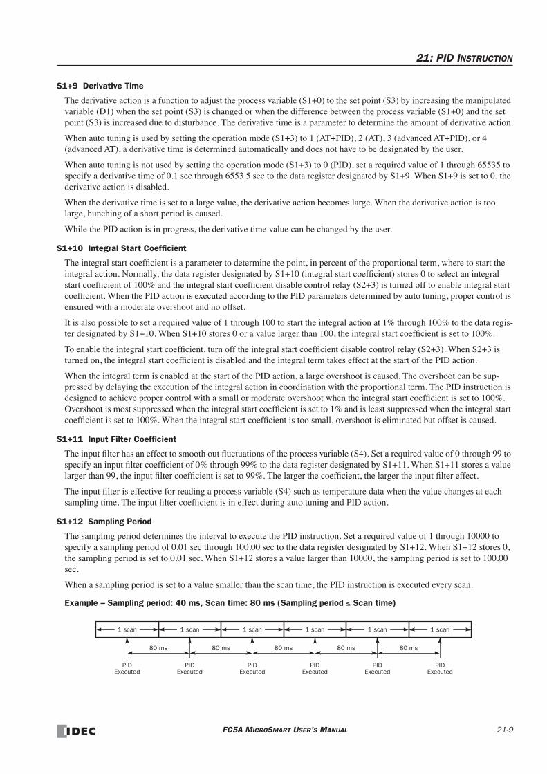
21: PID INSTRUCTION
S1+9 Derivative Time
The derivative action is a function to adjust the process variable (S1+0) to the set point (S3) by increasing the manipulated variable (D1) when the set point (S3) is changed or when the difference between the process variable (S1+0) and the set point (S3) is increased due to disturbance. The derivative time is a parameter to determine the amount of derivative action.
When auto tuning is used by setting the operation mode (S1+3) to 1 (AT+PID), 2 (AT), 3 (advanced AT+PID), or 4 (advanced AT), a derivative time is determined automatically and does not have to be designated by the user.
When auto tuning is not used by setting the operation mode (S1+3) to 0 (PID), set a required value of 1 through 65535 to specify a derivative time of 0.1 sec through 6553.5 sec to the data register designated by S1+9. When S1+9 is set to 0, the derivative action is disabled.
When the derivative time is set to a large value, the derivative action becomes large. When the derivative action is too large, hunching of a short period is caused.
While the PID action is in progress, the derivative time value can be changed by the user.
S1+10 Integral Start Coefficient
The integral start coefficient is a parameter to determine the point, in percent of the proportional term, where to start the integral action. Normally, the data register designated by S1+10 (integral start coefficient) stores 0 to select an integral start coefficient of 100% and the integral start coefficient disable control relay (S2+3) is turned off to enable integral start coefficient. When the PID action is executed according to the PID parameters determined by auto tuning, proper control is ensured with a moderate overshoot and no offset.
It is also possible to set a required value of 1 through 100 to start the integral action at 1% through 100% to the data regis-ter designated by S1+10. When S1+10 stores 0 or a value larger than 100, the integral start coefficient is set to 100%.
To enable the integral start coefficient, turn off the integral start coefficient disable control relay (S2+3). When S2+3 is turned on, the integral start coefficient is disabled and the integral term takes effect at the start of the PID action.
When the integral term is enabled at the start of the PID action, a large overshoot is caused. The overshoot can be sup-pressed by delaying the execution of the integral action in coordination with the proportional term. The PID instruction is designed to achieve proper control with a small or moderate overshoot when the integral start coefficient is set to 100%. Overshoot is most suppressed when the integral start coefficient is set to 1% and is least suppressed when the integral start coefficient is set to 100%. When the integral start coefficient is too small, overshoot is eliminated but offset is caused.
S1+11 Input Filter Coefficient
The input filter has an effect to smooth out fluctuations of the process variable (S4). Set a required value of 0 through 99 to specify an input filter coefficient of 0% through 99% to the data register designated by S1+11. When S1+11 stores a value larger than 99, the input filter coefficient is set to 99%. The larger the coefficient, the larger the input filter effect.
The input filter is effective for reading a process variable (S4) such as temperature data when the value changes at each sampling time. The input filter coefficient is in effect during auto tuning and PID action.
S1+12 Sampling Period
The sampling period determines the interval to execute the PID instruction. Set a required value of 1 through 10000 to specify a sampling period of 0.01 sec through 100.00 sec to the data register designated by S1+12. When S1+12 stores 0, the sampling period is set to 0.01 sec. When S1+12 stores a value larger than 10000, the sampling period is set to 100.00 sec.
When a sampling period is set to a value smaller than the scan time, the PID instruction is executed every scan.
Example – Sampling period: 40 ms, Scan time: 80 ms (Sampling period ≤ Scan time)
1 scan
80 ms 80 ms 80 ms 80 ms 80 ms
PIDExecuted
PIDExecuted
PIDExecuted
PIDExecuted
PIDExecuted
PIDExecuted
1 scan 1 scan 1 scan 1 scan 1 scan
FC5A MICROSMART USER’S MANUAL 21-9
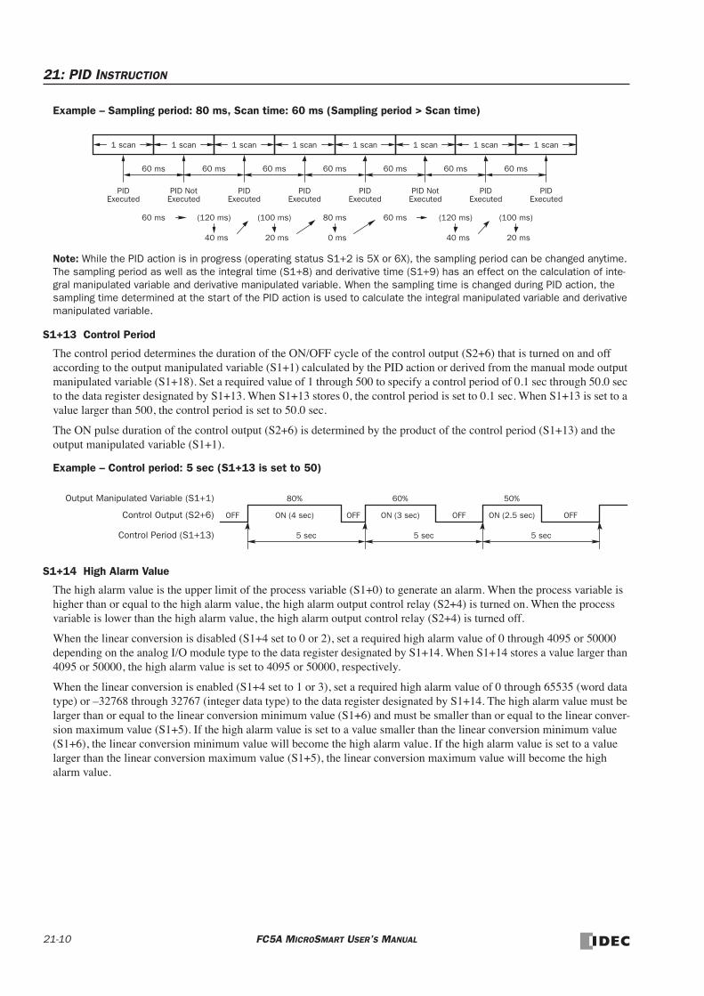
21: PID INSTRUCTION
Example – Sampling period: 80 ms, Scan time: 60 ms (Sampling period > Scan time)
Note: While the PID action is in progress (operating status S1+2 is 5X or 6X), the sampling period can be changed anytime. The sampling period as well as the integral time (S1+8) and derivative time (S1+9) has an effect on the calculation of inte-gral manipulated variable and derivative manipulated variable. When the sampling time is changed during PID action, the sampling time determined at the start of the PID action is used to calculate the integral manipulated variable and derivative manipulated variable.
S1+13 Control Period
The control period determines the duration of the ON/OFF cycle of the control output (S2+6) that is turned on and off according to the output manipulated variable (S1+1) calculated by the PID action or derived from the manual mode output manipulated variable (S1+18). Set a required value of 1 through 500 to specify a control period of 0.1 sec through 50.0 sec to the data register designated by S1+13. When S1+13 stores 0, the control period is set to 0.1 sec. When S1+13 is set to a value larger than 500, the control period is set to 50.0 sec.
The ON pulse duration of the control output (S2+6) is determined by the product of the control period (S1+13) and the output manipulated variable (S1+1).
Example – Control period: 5 sec (S1+13 is set to 50)
S1+14 High Alarm Value
The high alarm value is the upper limit of the process variable (S1+0) to generate an alarm. When the process variable is higher than or equal to the high alarm value, the high alarm output control relay (S2+4) is turned on. When the process variable is lower than the high alarm value, the high alarm output control relay (S2+4) is turned off.
When the linear conversion is disabled (S1+4 set to 0 or 2), set a required high alarm value of 0 through 4095 or 50000 depending on the analog I/O module type to the data register designated by S1+14. When S1+14 stores a value larger than 4095 or 50000, the high alarm value is set to 4095 or 50000, respectively.
When the linear conversion is enabled (S1+4 set to 1 or 3), set a required high alarm value of 0 through 65535 (word data type) or –32768 through 32767 (integer data type) to the data register designated by S1+14. The high alarm value must be larger than or equal to the linear conversion minimum value (S1+6) and must be smaller than or equal to the linear conver-sion maximum value (S1+5). If the high alarm value is set to a value smaller than the linear conversion minimum value (S1+6), the linear conversion minimum value will become the high alarm value. If the high alarm value is set to a value larger than the linear conversion maximum value (S1+5), the linear conversion maximum value will become the high alarm value.
60 ms
1 scan
60 ms 60 ms 60 ms 60 ms 60 ms 60 ms
PID
60 ms (120 ms)
40 ms
(100 ms)
20 ms
80 ms
0 ms
60 ms (120 ms)
40 ms
(100 ms)
20 ms
1 scan 1 scan 1 scan 1 scan 1 scan 1 scan 1 scan
ExecutedPID Not
ExecutedPID
ExecutedPID
ExecutedPID
ExecutedPID Not
ExecutedPID
ExecutedPID
Executed
5 sec 5 sec 5 sec
ON (4 sec) OFF ON (3 sec) ON (2.5 sec)OFF OFFOFFControl Output (S2+6)
80% 60% 50%Output Manipulated Variable (S1+1)
Control Period (S1+13)
21-10 FC5A MICROSMART USER’S MANUAL

21: PID INSTRUCTION
S1+15 Low Alarm Value
The low alarm value is the lower limit of the process variable (S1+0) to generate an alarm. When the process variable is lower than or equal to the low alarm value, the low alarm output control relay (S2+5) is turned on. When the process vari-able is higher than the low alarm value, the low alarm output control relay (S2+5) is turned off.
When the linear conversion is disabled (S1+4 set to 0 or 2), set a required low alarm value of 0 through 4095 or 50000 depending on the analog I/O module type to the data register designated by S1+15. When S1+15 stores a value larger than 4095 or 50000, the low alarm value is set to 4095 or 50000, respectively.
When the linear conversion is enabled (S1+4 set to 1 or 3), set a required low alarm value of 0 through 65535 (word data type) or –32768 through 32767 (integer data type) to the data register designated by S1+15. The low alarm value must be larger than or equal to the linear conversion minimum value (S1+6) and must be smaller than or equal to the linear conver-sion maximum value (S1+5). If the low alarm value is set to a value smaller than the linear conversion minimum value (S1+6), the linear conversion minimum value will become the low alarm value. If the low alarm value is set to a value larger than the linear conversion maximum value (S1+5), the linear conversion maximum value will become the low alarm value.
S1+16 Output Manipulated Variable Upper Limit
The value contained in the data register designated by S1+16 specifies the upper limit of the output manipulated variable (S1+1) in two ways: direct and proportional.
S1+16 Value 0 through 100When S1+16 contains a value 0 through 100, the value directly determines the upper limit of the output manipulated vari-able (S1+1). If the manipulated variable (D1) is greater than or equal to the upper limit value (S1+16), the upper limit value is outputted to the output manipulated variable (S1+1). Set a required value of 0 through 100 for the output manipu-lated variable upper limit to the data register designated by S1+16. When S1+16 stores a value larger than 100 (except 10001 through 10099), the output manipulated variable upper limit (S1+16) is set to 100. The output manipulated variable upper limit (S1+16) must be larger than the output manipulated variable lower limit (S1+17).
To enable the manipulated variable upper limit, turn on the output manipulated variable limit enable control relay (S2+2). When S2+2 is turned off, the output manipulated variable upper limit (S1+16) has no effect.
S1+16 Value 10001 through 10099 (disables Output Manipulated Variable Lower Limit S1+17)When S1+16 contains a value 10001 through 10099, the value minus 10000 determines the ratio of the output manipulated variable (S1+1) in proportion to the manipulated variable (D1) of 0 through 100. The output manipulated variable (S1+1) can be calculated by the following equation:
Output manipulated variable (S1+1) = Manipulated variable (D1) × (N – 10000)
where N is the value stored in the output manipulated variable upper limit (S1+16), 10001 through 10099.
If the manipulated variable (D1) is greater than or equal to 100, 100 multiplied by (N – 10000) is outputted to the output manipulated variable (S1+1). If D1 is less than or equal to 0, 0 is outputted to S1+1.
To enable the manipulated variable upper limit, turn on the output manipulated variable limit enable control relay (S2+2). When S2+2 is turned off, the output manipulated variable upper limit (S1+16) has no effect.
When S1+16 is set to a value 10001 through 10099, the output manipulated variable lower limit (S1+17) is disabled.
S1+17 Output Manipulated Variable Lower Limit
The value contained in the data register designated by S1+17 specifies the lower limit of the output manipulated variable (S1+1). Set a required value of 0 through 100 for the output manipulated variable lower limit to the data register desig-nated by S1+17. When S1+17 stores a value larger than 100, the output manipulated variable lower limit is set to 100. The output manipulated variable lower limit (S1+17) must be smaller than the output manipulated variable upper limit (S1+16).
To enable the output manipulated variable lower limit, turn on the output manipulated variable limit enable control relay (S2+2), and set the output manipulated variable upper limit (S1+16) to a value other than 10001 through 10099. When the manipulated variable (D1) is smaller than or equal to the specified lower limit, the lower limit value is outputted to the out-put manipulated variable (S1+1).
When the output manipulated variable limit enable control relay (S2+2) is turned off, the output manipulated variable lower limit (S1+17) has no effect.
FC5A MICROSMART USER’S MANUAL 21-11

21: PID INSTRUCTION
S1+18 Manual Mode Output Manipulated Variable
The manual mode output manipulated variable specifies the output manipulated variable (0 through 100) for manual mode. Set a required value of 0 through 100 for the manual mode output manipulated variable to the data register designated by S1+18. When S1+18 stores a value larger than 100, the manual mode output manipulated variable is set to 100.
To enable the manual mode, turn on the auto/manual mode control relay (S2+1). While in manual mode, the PID action is disabled. The specified value of the manual mode output manipulated variable (S1+18) is outputted to the output manipu-lated variable (S1+1) and the output manipulated variable for analog output module (S1+24). The control output (S2+6) is turned on and off according to the control period (S1+13) and the manual mode output manipulated variable (S1+18).
The S1+18 value has no effect on the manipulated value (D1) and the output manipulated variable % (S1+23).
Auto Tuning (AT) and Advanced Auto Tuning (Advanced AT)When auto tuning is selected with the operation mode (S1+3) set to 1 (AT+PID) or 2 (AT), the auto tuning is executed before starting PID control to determine PID parameters, such as proportional term (S1+7), integral time (S1+8), deriva-tive time (S1+9), and control action (S2+0) automatically. The MicroSmart uses the step response method to execute auto tuning. To enable auto tuning, set four parameters for auto tuning before executing the PID instruction, such as AT sampling period (S1+19), AT control period (S1+20), AT set point (S1+21), and AT output manipulated variable (S1+22).
When advanced auto tuning is selected with the operation mode (S1+3) set to 3 (advanced AT+PID) or 4 (advanced AT), most AT parameters are determined automatically and do not have to be designated by the user. Only when advanced auto tuning is used with S1+3 set to 4 (advanced AT), the user has to designate the AT set point (S1+21).
AT ParametersBefore executing auto tuning, AT parameters must be designated by the user as summarized in the table below.
Step Response MethodThe MicroSmart uses the step response method to execute auto tuning and determine PID parameters such as proportional term (S1+7), integral time (S1+8), derivative time (S1+9), and control action (S2+0) automatically. The auto tuning is executed in the following steps:
1. Calculate the maximum slope of the process variable (S1+0) before the process variable reaches the AT set point (S1+21).
2. Calculate the dead time based on the derived maximum slope.
3. Based on the maximum slope and dead time, calculate the four PID parameters.
Operation Mode (S1+3)AT sampling period
(S1+19)AT control
period (S1+20)AT set point
(S1+21)AT output manipulated
variable (S1+22)
0: PID action — — — —
1: AT (auto tuning) + PID actionBy user By user By user
By user (0 to 100)2: AT (auto tuning)
3: Advanced AT + PID action Automatic Automatic Automatic Automatic
4: Advanced AT Automatic Automatic By user Automatic
Process Variable (S1+0)
Dead Time
Maximum Slope
AT Set Point (S1+21)
21-12 FC5A MICROSMART USER’S MANUAL
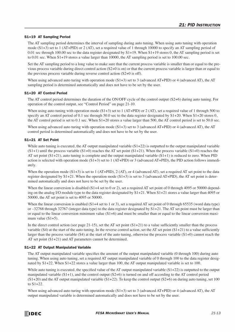
21: PID INSTRUCTION
S1+19 AT Sampling Period
The AT sampling period determines the interval of sampling during auto tuning. When using auto tuning with operation mode (S1+3) set to 1 (AT+PID) or 2 (AT), set a required value of 1 through 10000 to specify an AT sampling period of 0.01 sec through 100.00 sec to the data register designated by S1+19. When S1+19 stores 0, the AT sampling period is set to 0.01 sec. When S1+19 stores a value larger than 10000, the AT sampling period is set to 100.00 sec.
Set the AT sampling period to a long value to make sure that the current process variable is smaller than or equal to the pre-vious process variable during direct control action (S2+0 is on) or that the current process variable is larger than or equal to the previous process variable during reverse control action (S2+0 is off).
When using advanced auto turing with operation mode (S1+3) set to 3 (advanced AT+PID) or 4 (advanced AT), the AT sampling period is determined automatically and does not have to be set by the user.
S1+20 AT Control Period
The AT control period determines the duration of the ON/OFF cycle of the control output (S2+6) during auto tuning. For operation of the control output, see “Control Period” on page 21-10.
When using auto tuning with operation mode (S1+3) set to 1 (AT+PID) or 2 (AT), set a required value of 1 through 500 to specify an AT control period of 0.1 sec through 50.0 sec to the data register designated by S1+20. When S1+20 stores 0, the AT control period is set to 0.1 sec. When S1+20 stores a value larger than 500, the AT control period is set to 50.0 sec.
When using advanced auto turing with operation mode (S1+3) set to 3 (advanced AT+PID) or 4 (advanced AT), the AT control period is determined automatically and does not have to be set by the user.
S1+21 AT Set Point
While auto tuning is executed, the AT output manipulated variable (S1+22) is outputted to the output manipulated variable (S1+1) until the process variable (S1+0) reaches the AT set point (S1+21). When the process variable (S1+0) reaches the AT set point (S1+21), auto tuning is complete and the output manipulated variable (S1+1) is reduced to zero. When PID action is selected with operation mode (S1+3) set to 1 (AT+PID) or 3 (advanced AT+PID), the PID action follows immedi-ately.
When the operation mode (S1+3) is set to 1 (AT+PID), 2 (AT), or 4 (advanced AT), set a required AT set point to the data register designated by S1+21. When the operation mode (S1+3) is set to 3 (advanced AT+PID), the AT set point is deter-mined automatically and does not have to be set by the user.
When the linear conversion is disabled (S1+4 set to 0 or 2), set a required AT set point of 0 through 4095 or 50000 depend-ing on the analog I/O module type to the data register designated by S1+21. When S1+21 stores a value larger than 4095 or 50000, the AT set point is set to 4095 or 50000.
When the linear conversion is enabled (S1+4 set to 1 or 3), set a required AT set point of 0 through 65535 (word data type) or –32768 through 32767 (integer data type) to the data register designated by S1+21. The AT set point must be larger than or equal to the linear conversion minimum value (S1+6) and must be smaller than or equal to the linear conversion maxi-mum value (S1+5).
In the direct control action (see page 21-15), set the AT set point (S1+21) to a value sufficiently smaller than the process variable (S4) at the start of the auto tuning. In the reverse control action, set the AT set point (S1+21) to a value sufficiently larger than the process variable (S4) at the start of the auto tuning, otherwise the process variable (S1+0) cannot reach the AT set point (S1+21) and AT parameters cannot be determined.
S1+22 AT Output Manipulated Variable
The AT output manipulated variable specifies the amount of the output manipulated variable (0 through 100) during auto tuning. When using auto tuning, set a required AT output manipulated variable of 0 through 100 to the data register desig-nated by S1+22. When S1+22 stores a value larger than 100, the AT output manipulated variable is set to 100.
While auto tuning is executed, the specified value of the AT output manipulated variable (S1+22) is outputted to the output manipulated variable (S1+1), and the control output (S2+6) is turned on and off according to the AT control period (S1+20) and the AT output manipulated variable (S1+22). To keep the control output (S2+6) on during auto tuning, set 100 to S1+22.
When using advanced auto turing with operation mode (S1+3) set to 3 (advanced AT+PID) or 4 (advanced AT), the AT output manipulated variable is determined automatically and does not have to be set by the user.
FC5A MICROSMART USER’S MANUAL 21-13

21: PID INSTRUCTION
S1+23 Output Manipulated Variable %
While the PID action is in progress, the data register designated by S1+23 holds the manipulated variable, –32768 through 32767 (–327.68% through 327.67%), indicating the value to the second decimal place.
While manual mode is enabled with the auto/manual mode control relay (S2+1) set to on, S1+23 holds an indefinite value.
While auto tuning or advanced auto tuning is in progress, S1+23 holds an indefinite value.
S1+24 Output Manipulated Variable for Analog Output Module
While the PID action is in progress, the data register designated by S1+24 holds a value of 0 through 4095 or 50000, depending on the analog I/O module type. The value is converted from the value of 0 through 100 stored in S1+1 to repre-sent the output manipulated variable of 0% through 100%.
While manual mode is enabled with the auto/manual mode control relay (S2+1) set to on, S1+24 holds a value of 0 through 4095 or 50000 converted from the manual mode output manipulated variable (S1+18).
While auto tuning or advanced auto tuning is in progress, S1+24 holds a value of 0 through 4095 or 50000 read from the AT output manipulated variable (S1+22).
S1+25 Proportional Band Offset Value
When the proportional band is selected (S1+4 set to 2 or 3), the output manipulated variable (S1+1) of 0% through 100% can be shifted by an offset of –100% through 100%. Set a required offset value of –100 through 100 to the data register designated by S1+25 before executing auto tuning.
When the proportional gain is selected (S1+4 set to 0 or 1), the proportional band offset value (S1+25) has no effect.
S1+26 Derivative Gain
The derivative gain can be selected from 0% through 100%. When the derivative gain is set to a small value, the output manipulated variable (S1+1) is susceptible to an external noise or a change in the set point. When the derivative gain is set to a large value, the output manipulated variable (S1+1) becomes less susceptible to an external noise or a change in the set point, but stability is adversely affected during normal operation. Set a required derivative gain of 0 through 100 to the data register designated by S1+26 before executing auto tuning.
Recommended values are 20% through 30% when the process variable fluctuates or is subject to noise.
Source Operand S2 (Control Relay)Turn on or off appropriate outputs or internal relays starting with the operand designated by S2 before executing the PID instruction as required. Operands S2+4 through S2+7 are for read only to reflect the PID and auto tuning statuses.
Operand Function Description R/W
S2+0 Control actionON: Direct control action OFF: Reverse control action
R/W
S2+1 Auto/manual modeON: Manual mode OFF: Auto mode
R/W
S2+2Output manipulated variable limit enable
ON: Enable output manipulated variable upper and lower limits (S1+16 and S1+17) OFF: Disable output manipulated variable upper and lower limits (S1+16 and S1+17)
R/W
S2+3Integral start coefficient disable
ON: Disable integral start coefficient (S1+10) OFF: Enable integral start coefficient (S1+10)
R/W
S2+4 High alarm outputON: When process variable (S1+0) ≥ high alarm value (S1+14) OFF: When process variable (S1+0) < high alarm value (S1+14)
R
S2+5 Low alarm outputON: When process variable (S1+0) ≤ low alarm value (S1+15) OFF: When process variable (S1+0) > low alarm value (S1+15)
R
S2+6 Control output Goes on and off according to the AT parameters or PID calculation results R
S2+7 AT complete output Goes on when AT is complete or failed, and remains on until reset R
21-14 FC5A MICROSMART USER’S MANUAL
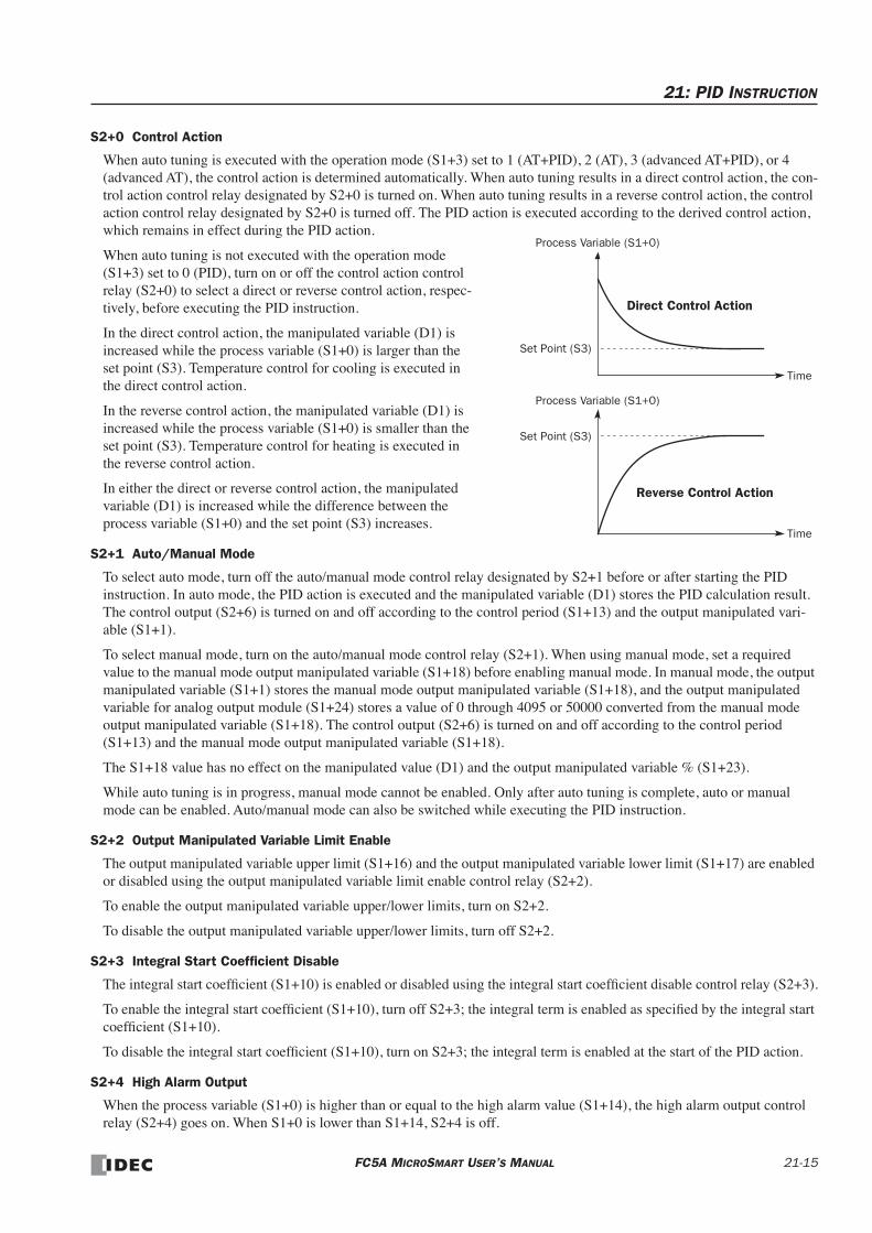
21: PID INSTRUCTION
S2+0 Control Action
When auto tuning is executed with the operation mode (S1+3) set to 1 (AT+PID), 2 (AT), 3 (advanced AT+PID), or 4 (advanced AT), the control action is determined automatically. When auto tuning results in a direct control action, the con-trol action control relay designated by S2+0 is turned on. When auto tuning results in a reverse control action, the control action control relay designated by S2+0 is turned off. The PID action is executed according to the derived control action, which remains in effect during the PID action.
When auto tuning is not executed with the operation mode (S1+3) set to 0 (PID), turn on or off the control action control relay (S2+0) to select a direct or reverse control action, respec-tively, before executing the PID instruction.
In the direct control action, the manipulated variable (D1) is increased while the process variable (S1+0) is larger than the set point (S3). Temperature control for cooling is executed in the direct control action.
In the reverse control action, the manipulated variable (D1) is increased while the process variable (S1+0) is smaller than the set point (S3). Temperature control for heating is executed in the reverse control action.
In either the direct or reverse control action, the manipulated variable (D1) is increased while the difference between the process variable (S1+0) and the set point (S3) increases.
S2+1 Auto/Manual Mode
To select auto mode, turn off the auto/manual mode control relay designated by S2+1 before or after starting the PID instruction. In auto mode, the PID action is executed and the manipulated variable (D1) stores the PID calculation result. The control output (S2+6) is turned on and off according to the control period (S1+13) and the output manipulated vari-able (S1+1).
To select manual mode, turn on the auto/manual mode control relay (S2+1). When using manual mode, set a required value to the manual mode output manipulated variable (S1+18) before enabling manual mode. In manual mode, the output manipulated variable (S1+1) stores the manual mode output manipulated variable (S1+18), and the output manipulated variable for analog output module (S1+24) stores a value of 0 through 4095 or 50000 converted from the manual mode output manipulated variable (S1+18). The control output (S2+6) is turned on and off according to the control period (S1+13) and the manual mode output manipulated variable (S1+18).
The S1+18 value has no effect on the manipulated value (D1) and the output manipulated variable % (S1+23).
While auto tuning is in progress, manual mode cannot be enabled. Only after auto tuning is complete, auto or manual mode can be enabled. Auto/manual mode can also be switched while executing the PID instruction.
S2+2 Output Manipulated Variable Limit Enable
The output manipulated variable upper limit (S1+16) and the output manipulated variable lower limit (S1+17) are enabled or disabled using the output manipulated variable limit enable control relay (S2+2).
To enable the output manipulated variable upper/lower limits, turn on S2+2.
To disable the output manipulated variable upper/lower limits, turn off S2+2.
S2+3 Integral Start Coefficient Disable
The integral start coefficient (S1+10) is enabled or disabled using the integral start coefficient disable control relay (S2+3).
To enable the integral start coefficient (S1+10), turn off S2+3; the integral term is enabled as specified by the integral start coefficient (S1+10).
To disable the integral start coefficient (S1+10), turn on S2+3; the integral term is enabled at the start of the PID action.
S2+4 High Alarm Output
When the process variable (S1+0) is higher than or equal to the high alarm value (S1+14), the high alarm output control relay (S2+4) goes on. When S1+0 is lower than S1+14, S2+4 is off.
Process Variable (S1+0)
Direct Control Action
Set Point (S3)
Time
Process Variable (S1+0)
Reverse Control Action
Set Point (S3)
Time
FC5A MICROSMART USER’S MANUAL 21-15

21: PID INSTRUCTION
S2+5 Low Alarm Output
When the process variable (S1+0) is lower than or equal to the low alarm value (S1+15), the low alarm output control relay (S2+5) goes on. When S1+0 is higher than S1+15, S2+5 is off.
S2+6 Control Output
During auto tuning in auto mode with the auto/manual mode control relay (S2+1) set to off, the control output (S2+6) is turned on and off according to the AT control period (S1+20) and AT output manipulated variable (S1+22).
During PID action in auto mode with the auto/manual mode control relay (S2+1) set to off, the control output (S2+6) is turned on and off according to the control period (S1+13) and the output manipulated variable (S1+1) calculated by the PID action.
While advanced auto tuning is in progress, the control output (S2+6) remains on.
In manual mode with the auto/manual mode control relay (S2+1) set to on, the control output (S2+6) is turned on and off according to the control period (S1+13) and the manual mode output manipulated variable (S1+18).
S2+7 AT Complete Output
The AT complete output control relay (S2+7) goes on when auto tuning is complete or failed, and remains on until reset. Operating status codes are stored to the operating status control register (S1+2). See page 21-4.
Source Operand S3 (Set Point)The PID action is executed to adjust the process variable (S1+0) to the set point (S3).
When the linear conversion is disabled (S1+4 set to 0 or 2), set a required set point value of 0 through 4095 or 50000, depending on the analog I/O module type, to the operand designated by S3. Valid operands are data register and constant.
When the linear conversion is enabled (S1+4 set to 1 or 3), designate a data register as operand S3 and set a required set point value of 0 through 65535 (word data type) or –32768 through 32767 (integer data type) to the data register desig-nated by S3. The set point value (S3) must be larger than or equal to the linear conversion minimum value (S1+6) and smaller than or equal to the linear conversion maximum value (S1+5).
When an invalid value is designated as a set point, the PID action is stopped and an error code is stored to the data register designated by S1+2. See “Operating Status” on page 21-4.
Source Operand S4 (Process Variable before Conversion)The PID instruction is designed to use analog input data from an analog I/O module as process variable. The analog I/O module converts the input signal to a digital value of 0 through 4095 or 50000, and stores the digital value to a data register depending on the mounting position of the analog I/O module and the analog input channel connected to the analog input source. Designate a data register as source operand S4 to store the process variable.
For the data register number to designate as source operand S4, see page 26-3. Specify the data register number shown under Data in the Configure Parameters dialog box as source operand S4 (process variable) of the PID instruction. The analog input data in the selected data register is used as the process variable of the PID instruction.
Destination Operand D1 (Manipulated Variable)The data register designated by destination operand D1 stores the manipulated variable of –32768 through 32767 calcu-lated by the PID action. When the calculation result is less than –32768, D1 stores –32768. When the calculation result is greater than 32767, D1 stores 32767. While the calculation result is less than –32768 or greater than 32767, the PID action still continues.
When the output manipulated variable limit is disabled (S2+2 set to off) while the PID action is in progress, the data regis-ter designated by S1+1 holds 0 through 100 of the manipulated variable (D1), omitting values less than 0 and greater than 100. The percent value in S1+1 determines the ON duration of the control output (S2+6) in proportion to the control period (S1+13).
When the output manipulated variable limit is enabled (S2+2 set to on), the manipulated variable (D1) is stored to the out-put manipulated variable (S1+1) according to the output manipulated variable upper limit (S1+16) and the output manipu-lated variable lower limit (S1+17) as summarized in the table below.
21-16 FC5A MICROSMART USER’S MANUAL
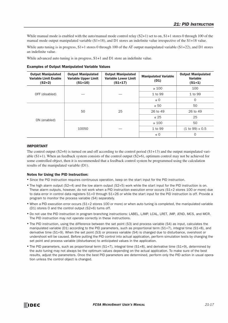
21: PID INSTRUCTION
While manual mode is enabled with the auto/manual mode control relay (S2+1) set to on, S1+1 stores 0 through 100 of the manual mode output manipulated variable (S1+18), and D1 stores an indefinite value irrespective of the S1+18 value.
While auto tuning is in progress, S1+1 stores 0 through 100 of the AT output manipulated variable (S1+22), and D1 stores an indefinite value.
While advanced auto tuning is in progress, S1+1 and D1 store an indefinite value.
Examples of Output Manipulated Variable Values
IMPORTANTThe control output (S2+6) is turned on and off according to the control period (S1+13) and the output manipulated vari-able (S1+1). When an feedback system consists of the control output (S2+6), optimum control may not be achieved for some controlled object, then it is recommended that a feedback control system be programmed using the calculation results of the manipulated variable (D1).
Notes for Using the PID Instruction:• Since the PID instruction requires continuous operation, keep on the start input for the PID instruction.
• The high alarm output (S2+4) and the low alarm output (S2+5) work while the start input for the PID instruction is on. These alarm outputs, however, do not work when a PID instruction execution error occurs (S1+2 stores 100 or more) due to data error in control data registers S1+0 through S1+26 or while the start input for the PID instruction is off. Provide a program to monitor the process variable (S4) separately.
• When a PID execution error occurs (S1+2 stores 100 or more) or when auto tuning is completed, the manipulated variable (D1) stores 0 and the control output (S2+6) turns off.
• Do not use the PID instruction in program branching instructions: LABEL, LJMP, LCAL, LRET, JMP, JEND, MCS, and MCR. The PID instruction may not operate correctly in these instructions.
• The PID instruction, using the difference between the set point (S3) and process variable (S4) as input, calculates the manipulated variable (D1) according to the PID parameters, such as proportional term (S1+7), integral time (S1+8), and derivative time (S1+9). When the set point (S3) or process variable (S4) is changed due to disturbance, overshoot or undershoot will be caused. Before putting the PID control into actual application, perform simulation tests by changing the set point and process variable (disturbance) to anticipated values in the application.
• The PID parameters, such as proportional term (S1+7), integral time (S1+8), and derivative time (S1+9), determined by the auto tuning may not always be the optimum values depending on the actual application. To make sure of the best results, adjust the parameters. Once the best PID parameters are determined, perform only the PID action in usual opera-tion unless the control object is changed.
Output Manipulated Variable Limit Enable
(S2+2)
Output Manipulated Variable Upper Limit
(S1+16)
Output Manipulated Variable Lower Limit
(S1+17)
Manipulated Variable(D1)
Output Manipulated Variable(S1+1)
OFF (disabled) — —
≥ 100 100
1 to 99 1 to 99
≤ 0 0
ON (enabled)
50 25
≥ 50 50
26 to 49 26 to 49
≤ 25 25
10050 —
≥ 100 50
1 to 99 (1 to 99) × 0.5
≤ 0 0
FC5A MICROSMART USER’S MANUAL 21-17

21: PID INSTRUCTION
Application ExamplesThe following two application examples demonstrate an advanced auto tuning and PID action to keep a heater temperature at 200°C.
In both examples, when the program is started, the PID instruction first executes advanced auto tuning to determine the AT parameters, such as AT sampling period, AT control period, AT set point, and AT output manipulated variable, using the temperature data inputted to the analog input module, then executes auto tuning to determine PID parameters such as pro-portional term, integral time, derivative time, sampling period, control period, and control action. When auto tuning is complete, PID action starts to control the temperature to 200°C using the derived PID parameters.
Example 1: ON/OFF Control Using Relay OutputThe heater is turned on and off according to the output manipulated variable calculated by the PID action. When the heater temperature is higher than or equal to 250°C, an alarm light is turned on by the high alarm output.
The analog input operating status is also monitored to force off the heater power switch and force on the high alarm light.
System Setup
Temperature Control by Auto Tuning and PID Action
Type K
High Alarm LightOutput Q1
Heater
+24V 0V 10 11 12 13 14 15DC OUT COM
DC IN 0 1 2 3 4 5 6 7
L N100-240VAC Ry.OUT
COM0Ry.OUTCOM1
Ry.OUTCOM3 11
Ry.OUTCOM2 100 1 2 3 4 5 6 7
Fuse
+
–
+
–
LOutput Q0
IN0
FC5A-C24R2 FC4A-L03AP1
Thermocouple
Process Variable after Conversion (S1+0)
Time
High Alarm Value (S1+14): 2500 (250°C)
Set Point (S3): 2000 (200°C)
AT Set Point (automatically determined)
Auto Tuning
PID Action
21-18 FC5A MICROSMART USER’S MANUAL

21: PID INSTRUCTION
Operand Settings
Note: When analog I/O module FC4A-L03AP1 is used for the PID instruction, select the binary data to make sure that the process variable takes a value of 0 through 4095.
Analog Input Data vs. Process Variable after Conversion
Operand Function Description Allocation No. (Value)S1+3 Operation mode Advanced AT (auto tuning) + PID action D3 (3)S1+4 Control mode Enable linear conversion, proportional band D4 (3)S1+5 Linear conversion maximum value 1300°C D5 (13000)S1+6 Linear conversion minimum value 0°C D6 (0)S1+10 Integral start coefficient 100% D10 (100)S1+11 Input filter coefficient 70% D11 (70)S1+14 High alarm value 250°C D14 (2500)S1+15 Low alarm value 0°C D15 (0)S1+25 Proportional band offset value 0% D25 (0)S1+26 Derivative gain 0% D26 (0)
S2+2Output manipulated variable limit enable
Disable output manipulated variable limits M2 (OFF)
S2+3 Integral start coefficient disable Enable integral start coefficient (S1+10) M3 (OFF)
S2+4 High alarm outputON: When temperature ≥ 250°C OFF: When temperature < 250°C
M4
S2+6 Control output
Remains on during advanced auto tuning; Goes on and off according to the control period (S1+13) and output manipulated vari-able (S1+1) during PID action
M6
S3 Set point 200°C D100 (2000)
S4 Process variableAnalog input data of analog I/O module 1, ana-log input channel 0; stores 0 through 4095
D760
Analog input operating status Stores 0 through 5 D761Analog input signal type Type K thermometer D762 (2)Analog input data type 12-bit data (0 to 4095) (Note) D763 (0)
D1 Manipulated variable Stores PID calculation result D50PID start input Starts to execute the PID instruction I0Heater power switch Turned on and off by control output M6 Q0
High alarm lightTurned on and off by high alarm output M4 and analog input error M11
Q1
Analog input errorTurns on when analog input operating status D761 is 3 or more
M11
High Alarm Value (S1+14): 2500 (250°C)
4095Linear Conversion Minimum Value (S1+6): 0 (0°C)
Linear Conversion Maximum Value (S1+5): 13000 (1300°C)
Set Point (S3): 2000 (200°C)AT Set Point (automatically determined)
Analog Input Data D760
Process Variable after Conversion (S1+0)
Process Variable before Conversion (S4)
0
FC5A MICROSMART USER’S MANUAL 21-19

21: PID INSTRUCTION
Ladder ProgramThe ladder diagram shown below describes an example of using the PID instruction. The user program must be modified according to the application and simulation must be performed before actual operation.
Set Analog Module Parameters (ANST) Dialog BoxWindLDR has a macro to program parameters for analog I/O modules. Place the cursor where to insert the ANST instruc-tion, click the right mouse button, and select Macro Instructions > Set Analog Module Parameters (ANST). In the ANST dialog box, press the Configure button under Slot 1, and program as shown below.
I0
When I0 is turned on, the ANST (analog macro) instruction stores parameters for the analog I/O module function.
The PIDST (PID macro) instruction also stores parameters for the PID function.
D760 is the analog input data of analog I/O module 1, ana-log input channel 0; stores 0 through 4095
When internal relay M4 (high alarm output) is turned on or M11 is turned on (analog input operating status is 3 or more), Q0 (heater output) is turned off and output Q1 (high alarm light) is turned on.
When M4 and M11 are off and M6 (control output) is turned on, Q0 (heater output) is turned on and output Q1 (high alarm light) is turned off.
When D761 (analog input operating status) stores 3 or more, internal relay M11 is turned on.
S1D0
S2M0
PIDST S3D100
NO.1L03AP1
ANSTSOTU
I0D1D50
S1D0
S2M0
S3D100
PID(I)0-4095
S4D760
M4
M6
Q1S
Q0
M11
REPS1 –D761
D1 –M11
CMP>=(W) S2 –3
M4 M11
Q0R
Q1R
I0
21-20 FC5A MICROSMART USER’S MANUAL

21: PID INSTRUCTION
Set PID Parameters (PIDST) Dialog BoxPlace the cursor where to insert the PIDST instruction, click the right mouse button, and select Macro Instructions > Set PID Parameters (PIDST). In the PIDST dialog box, program as shown below.
PID Control (PID) Dialog Box
S1+3 Operation mode S1+14 High alarm valueS1+4 Control mode S1+15 Low alarm valueS1+5 Linear conversion maximum value S1+25 Proportional band offset valueS1+6 Linear conversion minimum value S1+26 Derivative gainS1+10 Integral start coefficient S2+2 Output manipulated variable limit enableS1+11 Input filter coefficient S2+3 Integral start coefficient disable
S3 Set point
S1+3
S2+3
S3
S1+10
S1+4
S1+5S1+6
S1+14S1+11
S1+15
S2+2
S1+25
S1+26
Select options and operands as with the PID instruction.
FC5A MICROSMART USER’S MANUAL 21-21

21: PID INSTRUCTION
Example 2: ON/OFF Control Using Analog OutputThe output manipulated variable for analog output module (S1+24) of the PID instruction is moved to the analog output data (D772) and the analog I/O module sends out a voltage output of 0 to 10V DC. The analog output is then connected to a thyristor unit which controls the AC power using phase control.
System Setup
Temperature Control by Auto Tuning and PID Action
Operand Settings for Analog I/O ModuleAnalog Channel
Function Description Allocation No. (Value)
Input Channel 0
Analog input dataAnalog input data of analog I/O module 1, ana-log input channel 0; stores 0 through 4095
D760
Analog input operating status Stores 0 through 5 D761Analog input signal type Type K thermometer D762 (2)Analog input data type 12-bit data (0 to 4095) D763 (0)
Output
Analog output data 0 to 4095 D772Analog output operating status Stores 0 through 4 D773Analog output signal type Voltage output (0 to 10V DC) D774 (0)Analog output data type 12-bit data (0 to 4095) D775 (0)
Type K
Heater
+24V 0V 10 11 12 13 14 15DC OUT COM
DC IN 0 1 2 3 4 5 6 7
L N100-240VAC Ry.OUT
COM0Ry.OUTCOM1
Ry.OUTCOM3 11
Ry.OUTCOM2 100 1 2 3 4 5 6 7
Fuse
+
–
+
– IN0
FC5A-C24R2 FC4A-L03AP1
Thermocouple
1
2L2
3
L1
Thyristor Unit
+
–
OUT
Process Variable after Conversion (S1+0)
Time
High Alarm Value (S1+14): 2500 (250°C)
Set Point (S3): 2000 (200°C)
AT Set Point (automatically determined)
Auto Tuning
PID Action
21-22 FC5A MICROSMART USER’S MANUAL

21: PID INSTRUCTION
Ladder ProgramThe ladder diagram shown below describes an example of using the PID instruction. The user program must be modified according to the application and simulation must be performed before actual operation.
Programming in the dialog boxes of the ANST (Set Analog Module Parameters), PIDST (Set PID Parameters), and PID (PID Control) instructions are the same as the preceding example.
Notes for Using Ladder Refresh Type Analog Input Modules:• When using analog input module FC4A-J4CN1 with Pt100 or Ni100 inputs, use the XYFS and CVXTY instructions to convert
the 0-6,000 input to 0-50,000 input and store the result to the process variable (S4) of the PID instruction.
• When using analog input module FC4A-J4CN1 with Pt1000 or Ni1000 inputs, use the XYFS and CVXTY instructions to con-vert the 0-60,000 input to 0-50,000 input and store the result to the process variable (S4) of the PID instruction.
• When using analog input module FC4A-J8AT1, keep the operation within the temperature range where the thermistor shows linear characteristics.
• When using analog input module FC4A-J8AT1, use the XYFS and CVXTY instructions to convert the 0-4,000 input to 0-50,000 input and store the result to the process variable (S4) of the PID instruction.
• When using analog output module FC4A-K2C1 with voltage outputs, use the XYFS and CVXTY instructions to convert the output manipulated variable for analog output module (S1+24) and store the result to the data register designated as ana-log output data of the analog output module.
• The following example demonstrates a program for analog input module FC4A-J4CN1 to convert Pt1000 or Ni1000 analog input data in D410 to a value within the range between 0 and 50,000, and store the result to D510.
I0
When I0 is turned on, the ANST (analog macro) instruc-tion stores parameters for the analog I/O module func-tion.
The PIDST (PID macro) instruction also stores parame-ters for the PID function.
D760 is the analog input data of analog I/O module 1, analog input channel 0; stores 0 through 4095
When internal relay M4 (high alarm output) is turned on or M11 is turned on (analog input operating status is 3 or more), 0 is set to D772 (analog output data), turning off the heater power.
When M4 and M11 are off, D24 (output manipulated variable for analog output module S1+24) of the PID instruction is moved to D772 (analog output data).
When D761 (analog input operating status) stores 3 or more, internal relay M11 is turned on.
S1D0
S2M0
PIDST S3D100
NO.1L03AP1
ANSTSOTU
I0D1D50
S1D0
S2M0
S3D100
PID(I)0-4095
S4D760
M4
M11
REPS1 –D761
D1 –M11
CMP>=(W) S2 –3
M4 M11
I0
S1 –0
D1 –D772
MOV(W) REP
S1 –D24
D1 –D772
MOV(W) REP
M8120 is the initialize pulse special internal relay.
At startup, XYFS specifies two points.
When input I0 is on, CVXTY converts the value in D410 and stores the result to D510.
M8120XYFS(W) Y1
50000
END
I0CVXTY(W) D1
D510
S11
X00
Y00
X160000
S11
S2D410
FC5A MICROSMART USER’S MANUAL 21-23

21: PID INSTRUCTION
21-24 FC5A MICROSMART USER’S MANUAL

22: DUAL / TEACHING TIMER INSTRUCTIONS
IntroductionDual timer instructions generate ON/OFF pulses of required durations from a designated output, internal relay, or shift register bit. Four dual timers are available and the ON/OFF duration can be selected from 1 ms up to 65535 sec.
Teaching timer instruction measures the ON duration of the start input for the teaching timer instruction and stores the measured data to a designated data register, which can be used as a preset value for a timer instruction.
DTML (1-sec Dual Timer)
DTIM (100-ms Dual Timer)
DTMH (10-ms Dual Timer)
DTMS (1-ms Dual Timer)
Applicable CPU Modules
FC5A-C10R2/C FC5A-C16R2/C FC5A-C24R2/C FC5A-D16RK1/RS1 FC5A-D32K3/S3
X X X X X
While input is on, destination operand D1 repeats to turn on and off for a duration designated by operands S1 and S2, respectively.
The time range is 0 through 65535 sec.
S1*****
D1*****
DTML S2*****
D2*****
While input is on, destination operand D1 repeats to turn on and off for a duration designated by operands S1 and S2, respectively.
The time range is 0 through 6553.5 sec.
S1*****
D1*****
DTIM S2*****
D2*****
While input is on, destination operand D1 repeats to turn on and off for a duration designated by operands S1 and S2, respectively.
The time range is 0 through 655.35 sec.
S1*****
D1*****
DTMH S2*****
D2*****
While input is on, destination operand D1 repeats to turn on and off for a duration designated by operands S1 and S2, respectively.
The time range is 0 through 65.535 sec.
S1*****
D1*****
DTMS S2*****
D2*****
FC5A MICROSMART USER’S MANUAL 22-1
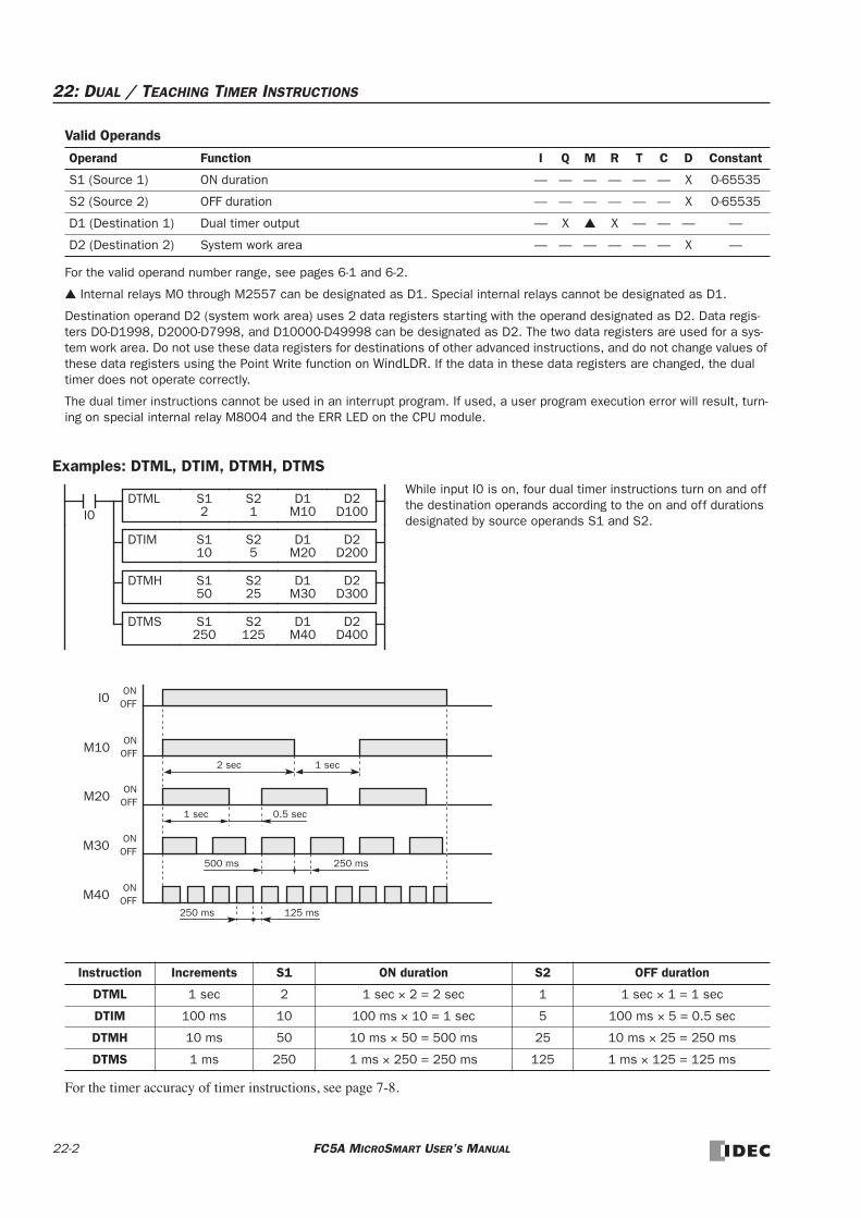
22: DUAL / TEACHING TIMER INSTRUCTIONS
Valid Operands
For the valid operand number range, see pages 6-1 and 6-2.
Internal relays M0 through M2557 can be designated as D1. Special internal relays cannot be designated as D1.
Destination operand D2 (system work area) uses 2 data registers starting with the operand designated as D2. Data regis-ters D0-D1998, D2000-D7998, and D10000-D49998 can be designated as D2. The two data registers are used for a sys-tem work area. Do not use these data registers for destinations of other advanced instructions, and do not change values of these data registers using the Point Write function on WindLDR. If the data in these data registers are changed, the dual timer does not operate correctly.
The dual timer instructions cannot be used in an interrupt program. If used, a user program execution error will result, turn-ing on special internal relay M8004 and the ERR LED on the CPU module.
Examples: DTML, DTIM, DTMH, DTMS
For the timer accuracy of timer instructions, see page 7-8.
Operand Function I Q M R T C D Constant
S1 (Source 1) ON duration — — — — — — X 0-65535
S2 (Source 2) OFF duration — — — — — — X 0-65535
D1 (Destination 1) Dual timer output — X X — — — —
D2 (Destination 2) System work area — — — — — — X —
Instruction Increments S1 ON duration S2 OFF duration
DTML 1 sec 2 1 sec × 2 = 2 sec 1 1 sec × 1 = 1 sec
DTIM 100 ms 10 100 ms × 10 = 1 sec 5 100 ms × 5 = 0.5 sec
DTMH 10 ms 50 10 ms × 50 = 500 ms 25 10 ms × 25 = 250 ms
DTMS 1 ms 250 1 ms × 250 = 250 ms 125 1 ms × 125 = 125 ms
500 ms 250 ms
I0D2
D100
While input I0 is on, four dual timer instructions turn on and off the destination operands according to the on and off durations designated by source operands S1 and S2.
S12
D1M10
DTML S21
D2D200
S110
D1M20
DTIM S25
D2D300
S150
D1M30
DTMH S225
D2D400
S1250
D1M40
DTMS S2125
M10ON
OFF
M20ON
OFF
M30ONOFF
I0ONOFF
2 sec
M40ONOFF
1 sec
1 sec 0.5 sec
250 ms 125 ms
22-2 FC5A MICROSMART USER’S MANUAL

22: DUAL / TEACHING TIMER INSTRUCTIONS
TTIM (Teaching Timer)
Applicable CPU Modules
Valid Operands
For the valid operand number range, see pages 6-1 and 6-2.
Destination operand D1 (measured value) uses 3 data registers starting with the operand designated as D1. Data registers D0-D1997, D2000-D7997, and D10000-D49997 can be designated as D1. Subsequent two data registers starting with destination operand D1+1 are used for a system work area. Do not use these two data registers for destinations of other advanced instructions, and do not change values of these data registers using the Point Write function on WindLDR. If the data in these data registers are changed, the teaching timer does not operate correctly.
The teaching timer instruction cannot be used in an interrupt program. If used, a user program execution error will result, turning on special internal relay M8004 and the ERR LED on the CPU module.
Examples: TTIM
The following example demonstrates a program to measure the ON duration of input I0 and to use the ON duration as a preset value for 100-ms timer instruction TIM.
FC5A-C10R2/C FC5A-C16R2/C FC5A-C24R2/C FC5A-D16RK1/RS1 FC5A-D32K3/S3
X X X X X
Operand Function I Q M R T C D Constant
D1 (Destination 1) Measured value — — — — — — X —
While input is on, the ON duration is measured in units of 100 ms and the measured value is stored to a data register designated by destination operand D1.
The measured time range is 0 through 6553.5 sec.
TTIM D1*****
I0D1
D100
When input I0 is turned on, TTIM resets data register D100 to zero and starts to store the ON duration of input I0 to data register D100, measured in units of 100 ms.
When input I0 is turned off, TTIM stops the measurement, and data register D100 main-tains the measured value of the ON duration.
TTIM
D100 Value
I0ON
OFF1500 ms
0 15
I0D1
D100
When input I1 is turned on, 100-ms timer T0 starts to operate with a preset value stored in data register D0.
While input I0 is on, TTIM measures the ON duration of input I0 and stores the measured value in units of 100 ms to data regis-ter D100.
When input I0 is turned off, MOV(W) stores the D100 value to data register D0 as a preset value for timer T0.
TTIM
I1TIMD0
T0
I0SOTD REPS1 –
D100D1 –D0
MOV(W)
FC5A MICROSMART USER’S MANUAL 22-3

22: DUAL / TEACHING TIMER INSTRUCTIONS
22-4 FC5A MICROSMART USER’S MANUAL

23: INTELLIGENT MODULE ACCESS INSTRUCTIONS
IntroductionIntelligent module access instructions are used to read or write data between the CPU module and a maximum of seven intelligent modules while the CPU module is running or when the CPU module is stopped.
Intelligent Module Access OverviewThe Run Access Read instruction reads data from the designated address in the intelligent module and stores the read data to the designated operand while the CPU module is running. The Run Access Write instruction writes data from the desig-nated operand to the designated address in the intelligent module while the CPU module is running.
The Stop Access Read instruction reads data from the designated address in the intelligent module and stores the read data to the designated operand when the CPU module is stopped. The Stop Access Write instruction writes data from the desig-nated operand to the designated address in the intelligent module when the CPU module is stopped.
While the CPU module is running and the input is on, RUNA READ is executed to read data from the intelligent module, and RUNA WRITE to write data to the intelli-gent module.
RUNA(*)READ ******
ONRUNA(*)READ ******
OFF
RUNA(*)WRITE ******
RUNA(*)READ ******
STPA(*)READ ******
STPA(*)WRITE ******
STPA(*)READ ******
STPA(*)WRITE ******
RUNA(*)WRITE ******
ONRUNA(*)WRITE ******
OFF
OFF
OFF
Read
Write
Intelligent Module
Write
ReadWhen the CPU module is stopped, STPA READ is executed to read data from the intelligent module, and STPA WRITE to write data to the intelligent module.
Intelligent ModuleData movement when the CPU module is stopped
Data movement while the CPU module is running
FC5A MICROSMART USER’S MANUAL 23-1

23: INTELLIGENT MODULE ACCESS INSTRUCTIONS
RUNA READ (Run Access Read)
Applicable CPU Modules
Valid Operands (Run Access Read)
For the valid operand number range, see pages 6-1 and 6-2.
DATA: Specify the first operand number to store the data read from the intelligent module.
Internal relays M0 through M2557 can be designated as DATA. Special internal relays cannot be desig-nated as DATA.
When T (timer) or C (counter) is used as DATA for Run Access Read, the data read from the intelligent module is stored as a preset value which can be 0 through 65535.
All data registers, including special data registers and expansion data registers, can be designated as DATA.
STATUS: Specify a data register to store the operating status code. Data registers D0-D1999 and D10000-D49999 can be designated as STATUS. Special data registers and expansion data registers cannot be designated. For status code description, see page 23-6.
SLOT: Enter the slot number where the intelligent module is mounted. A maximum of seven intelligent modules can be used.
ADDRESS: Specify the first address in the intelligent module to read data from.
BYTE: Specify the quantity of data to read in bytes.
The RUNA READ instruction cannot be used in an interrupt program. If used, a user program execution error will result, turn-ing on special internal relay M8004 and the ERR LED on the CPU module.
Valid Data Types
FC5A-C10R2/C FC5A-C16R2/C FC5A-C24R2/C FC5A-D16RK1/RS1 FC5A-D32K3/S3
— — X X X
Operand Function I Q M R T C D Constant Repeat
DATA First operand number to store read data — X X X X X — —
STATUS Operating status code — — — — — — X — —
SLOT Intelligent module slot number — — — — — — — 1-7 —
ADDRESS First address in intelligent module to read data from — — — — — — — 0-127 —
BYTE Bytes of data to read — — — — — — — 1-127 —
W (word) X
I (integer) X
D (double word) —
L (long) —
F (float) —
While input is on, data is read from the area starting at ADDRESS in the intelligent module designated by SLOT and stored to the operand designated by DATA.
BYTE designates the quantity of data to read.
STATUS stores the operating status code.
DATA*****
SLOT*
STATUS*****
BYTE***
ADDRESS***
RUNA(*)READ
When a bit operand such as I (input), Q (output), M (internal relay), or R (shift register) is desig-nated as DATA, 16 points are used.
When a word operand such as T (timer), C (counter), or D (data register) is designated as DATA, 1 point is used.
23-2 FC5A MICROSMART USER’S MANUAL

23: INTELLIGENT MODULE ACCESS INSTRUCTIONS
RUNA WRITE (Run Access Write)
Applicable CPU Modules
Valid Operands (Run Access Write)
For the valid operand number range, see pages 6-1 and 6-2.
DATA: Specify the first operand number to extract the data to write to the intelligent module.
When T (timer) or C (counter) is used as DATA for Run Access Write, the timer/counter current value is written to the intelligent module.
All data registers, including special data registers and expansion data registers, can be designated as DATA.
When a constant is designated as DATA, Repeat cannot be selected. For details about the data movement with or without Repeat, see page 23-7.
STATUS: Specify a data register to store the operating status code. Data registers D0-D1999 and D10000-D49999 can be designated as STATUS. Special data registers and expansion data registers cannot be designated. For status code description, see page 23-6.
SLOT: Enter the slot number where the intelligent module is mounted. A maximum of seven intelligent modules can be used.
ADDRESS: Specify the first address in the intelligent module to store the data.
BYTE: Specify the quantity of data to write in bytes.
The RUNA WRITE instruction cannot be used in an interrupt program. If used, a user program execution error will result, turn-ing on special internal relay M8004 and the ERR LED on the CPU module.
Valid Data Types
FC5A-C10R2/C FC5A-C16R2/C FC5A-C24R2/C FC5A-D16RK1/RS1 FC5A-D32K3/S3
— — X X X
Operand Function I Q M R T C D Constant Repeat
DATA First operand number to extract data from X X X X X X X X X
STATUS Operating status code — — — — — — X — —
SLOT Intelligent module slot number — — — — — — — 1-7 —
ADDRESS First address in intelligent module to write data to — — — — — — — 0-127 —
BYTE Bytes of data to write — — — — — — — 1-127 —
W (word) X
I (integer) X
D (double word) —
L (long) —
F (float) —
While input is on, data in the area starting at the operand designated by DATA is written to ADDRESS in the intelligent module designated by SLOT.
BYTE designates the quantity of data to write.
STATUS stores the operating status code.
DATA(R)*****
SLOT*
STATUS*****
BYTE***
ADDRESS***
RUNA(*)WRITE
When a bit operand such as I (input), Q (output), M (internal relay), or R (shift register) is desig-nated as DATA, 16 points are used.
When a word operand such as T (timer), C (counter), or D (data register) is designated as DATA, 1 point is used.
FC5A MICROSMART USER’S MANUAL 23-3

23: INTELLIGENT MODULE ACCESS INSTRUCTIONS
STPA READ (Stop Access Read)
Note: STPA READ and STPA WRITE instructions can be used 64 times in a user program. When more than 64 STPA READ and STPA WRITE instructions are used in a user program, the excess instructions are not executed and error code 7 is stored in the data register designated as STATUS.
Applicable CPU Modules
Valid Operands (Stop Access Read)
For the valid operand number range, see pages 6-1 and 6-2.
DATA: Specify the first operand number to store the data read from the intelligent module.
Internal relays M0 through M2557 can be designated as DATA. Special internal relays cannot be desig-nated as DATA.
When T (timer) or C (counter) is used as DATA for Stop Access Read, the data read from the intelligent module is stored as a preset value which can be 0 through 65535.
All data registers, including special data registers and expansion data registers, can be designated as DATA.
STATUS: Specify a data register to store the operating status code. Data registers D0-D1999 and D10000-D49999 can be designated as STATUS. Special data registers and expansion data registers cannot be designated. For status code description, see page 23-6.
SLOT: Enter the slot number where the intelligent module is mounted. A maximum of seven intelligent modules can be used.
ADDRESS: Specify the first address in the intelligent module to read data from.
BYTE: Specify the quantity of data to read in bytes.
The STPA READ instruction cannot be used in an interrupt program. If used, a user program execution error will result, turn-ing on special internal relay M8004 and the ERR LED on the CPU module.
If a STPA READ instruction is programmed between MCS and MCR instructions, the STPA READ instruction is executed when the CPU module is stopped regardless whether the input condition for the MCS instruction is on or off. For MCS and MCR instructions, see page 7-23.
Valid Data Types
FC5A-C10R2/C FC5A-C16R2/C FC5A-C24R2/C FC5A-D16RK1/RS1 FC5A-D32K3/S3
— — X X X
Operand Function I Q M R T C D Constant Repeat
DATA First operand number to store read data — X X X X X — —
STATUS Operating status code — — — — — — X — —
SLOT Intelligent module slot number — — — — — — — 1-7 —
ADDRESS First address in intelligent module to read data from — — — — — — — 0-127 —
BYTE Bytes of data to read — — — — — — — 1-127 —
W (word) X
I (integer) X
D (double word) —
L (long) —
F (float) —
When the CPU module stops, data is read from the area starting at ADDRESS in the intelligent module designated by SLOT and stored to the operand designated by DATA.
BYTE designates the quantity of data to read.
STATUS stores the operating status code.
DATA*****
SLOT*
STATUS*****
BYTE***
ADDRESS***
STPA(*)READ
Start input is not needed for this instruction.
When a bit operand such as I (input), Q (output), M (internal relay), or R (shift register) is desig-nated as DATA, 16 points are used.
When a word operand such as T (timer), C (counter), or D (data register) is designated as DATA, 1 point is used.
23-4 FC5A MICROSMART USER’S MANUAL

23: INTELLIGENT MODULE ACCESS INSTRUCTIONS
STPA WRITE (Stop Access Write)
Note: STPA READ and STPA WRITE instructions can be used 64 times in a user program. When more than 64 STPA READ and STPA WRITE instructions are used in a user program, the excess instructions are not executed and error code 7 is stored in the data register designated as STATUS.
Applicable CPU Modules
Valid Operands (Run Access Write)
For the valid operand number range, see pages 6-1 and 6-2.
DATA: Specify the first operand number to extract the data to write to the intelligent module.
When T (timer) or C (counter) is used as DATA for Stop Access Write, the timer/counter current value is written to the intelligent module.
All data registers, including special data registers and expansion data registers, can be designated as DATA.
When a constant is designated as DATA, Repeat cannot be selected. For details about the data movement with or without Repeat, see page 23-7.
STATUS: Specify a data register to store the operating status code. Data registers D0-D1999 and D10000-D49999 can be designated as STATUS. Special data registers and expansion data registers cannot be designated. For status code description, see page 23-6.
SLOT: Enter the slot number where the intelligent module is mounted. A maximum of seven intelligent modules can be used.
ADDRESS: Specify the first address in the intelligent module to store the data.
BYTE: Specify the quantity of data to write in bytes.
The STPA WRITE instruction cannot be used in an interrupt program. If used, a user program execution error will result, turn-ing on special internal relay M8004 and the ERR LED on the CPU module.
If a STPA WRITE instruction is programmed between MCS and MCR instructions, the STPA WRITE instruction is executed when the CPU module is stopped regardless whether the input condition for the MCS instruction is on or off. For MCS and MCR instructions, see page 7-23.
Valid Data Types
FC5A-C10R2/C FC5A-C16R2/C FC5A-C24R2/C FC5A-D16RK1/RS1 FC5A-D32K3/S3
— — X X X
Operand Function I Q M R T C D Constant Repeat
DATA First operand number to extract data from X X X X X X X X X
STATUS Operating status code — — — — — — X — —
SLOT Intelligent module slot number — — — — — — — 1-7 —
ADDRESS First address in intelligent module to write data to — — — — — — — 0-127 —
BYTE Bytes of data to write — — — — — — — 1-127 —
W (word) X
I (integer) X
D (double word) —
L (long) —
F (float) —
When the CPU module stops, data in the area starting at the operand designated by DATA is written to ADDRESS in the intelligent module designated by SLOT.
BYTE designates the quantity of data to write.
STATUS stores the operating status code.
DATA(R)*****
SLOT*
STATUS*****
BYTE***
ADDRESS***
STPA(*)WRITE
Start input is not needed for this instruction.
When a bit operand such as I (input), Q (output), M (internal relay), or R (shift register) is desig-nated as DATA, 16 points are used.
When a word operand such as T (timer), C (counter), or D (data register) is designated as DATA, 1 point is used.
FC5A MICROSMART USER’S MANUAL 23-5

23: INTELLIGENT MODULE ACCESS INSTRUCTIONS
Intelligent Module Access Status CodeThe data register designated as STATUS stores a status code to indicate the operating status and error of the intelligent module access operation. When status code 1, 3, or 7 is stored, take a corrective measure as described in the table below:
STPA Execution during Program DownloadWhen downloading a user program, the CPU module is automatically stopped as default. Depending on the timing of the initiation of the download and the total time to execute all STPA Read and Write instructions, some of the STPA instruc-tions may not be executed. If this is the case, manually stop the CPU module. After more than 1 second, initiate user pro-gram download as shown in the chart below.
STPA Execution between MCS and MCR InstructionsWhen the CPU module stops, STPA instructions programmed between MCS and MCR instructions are executed whether the input to the MCS instructions is on or off. For MCS and MCR instructions, see page 7-23.
Status Code
Status Description RUNA STPA
0 Normal Intelligent module access is normal. X X
1 Bus errorThe intelligent module is not installed correctly.Power down the MicroSmart modules, and re-install the intelli-gent module correctly.
X X
3 Invalid module numberThe designated module number is not found.Confirm the intelligent module number and correct the program.
X X
7 Excessive multiple usageMore than 64 STPA READ and STPA WRITE instructions are used. Eliminate the excess instructions.
— X
STPA instructions
CPU module
One cycle to execute all STPAs
Run
Power up
Stop
Initiate downloadAutomatic stop
Executed Not executed
Actual start to download
STPA instructions
CPU module
One cycle to execute all STPAs
Run
Power up
Stop
Manual stop
Executed
Initiate download
More than 1 sec
Automatic Stop Sequence
Manual Stop Sequence
23-6 FC5A MICROSMART USER’S MANUAL

23: INTELLIGENT MODULE ACCESS INSTRUCTIONS
Example: RUNA READThe following example illustrates the data movement of the RUNA READ instruction. The data movement of the STPA READ is the same as the RUNA READ instruction.
Example: RUNA WRITE without RepeatThe following example illustrates the data movement of the RUNA WRITE instruction without repeat designation. The data movement of the STPA WRITE is the same as the RUNA WRITE instruction.
Example: RUNA WRITE with RepeatThe following example illustrates the data movement of the RUNA WRITE instruction with repeat designation. The data movement of the STPA WRITE is the same as the RUNA WRITE instruction.
While input I0 is on, data of 5 bytes is read from the area starting at address 1 in intelligent mod-ule 1 and stored to the 5-byte area in data regis-ters starting at D9.
Status code is stored in data register D100.
I0DATAD9
SLOT1
STATUSD100
BYTE5
ADDRESS1READ
RUNA(W)
02hD9
04hD10
D11
High
01h
Low
03h
05h
00hAddress 0
01hAddress 1
02hAddress 2
03hAddress 3
04hAddress 4
05hAddress 5
CPU Module Intelligent Module 1
While input I1 is on, data in data register D19 is written to the 5-byte area starting at address 1 in intelligent module 1.
Status code is stored in data register D101.
I1DATA –D19
SLOT1
STATUSD101
BYTE5
ADDRESS1WRITE
RUNA(W)
02hD19
D20
D21
High
01h
Low Address 0
01hAddress 1
02hAddress 2
01hAddress 3
02hAddress 4
01hAddress 5
CPU Module Intelligent Module 1
While input I2 is on, data in 5-byte area starting at data register D22 is written to the 5-byte area starting at address 7 in intelligent module 1.
Status code is stored in data register D102.
I2DATA R
D22SLOT
1STATUSD102
BYTE5
ADDRESS7WRITE
RUNA(W)
04hD22
06hD23
D24
High
03h
Low
05h
07h
Address 6
03hAddress 7
04hAddress 8
05hAddress 9
06hAddress 10
07hAddress 11
CPU Module Intelligent Module 1
FC5A MICROSMART USER’S MANUAL 23-7

23: INTELLIGENT MODULE ACCESS INSTRUCTIONS
23-8 FC5A MICROSMART USER’S MANUAL

24: TRIGONOMETRIC FUNCTION INSTRUCTIONS
IntroductionTrigonometric function instructions are used for conversion between radian and degree values, conversion from radian value to sine, cosine, and tangent, and also calculation of arc sine, arc cosine, and arc tangent values.
RAD (Degree to Radian)
Applicable CPU Modules
Valid Operands
For the valid operand number range, see pages 6-1 and 6-2.
When the conversion result is not within the range between –3.402823 × 1038 and –1.175495 × 10–38 or between 1.175495 × 10–38 and 3.402823 × 1038, special internal relay M8003 (carry or borrow) is turned on except when the con-version result is 0. When the conversion result is between –1.175495 × 10–38 and 1.175495 × 10–38, the destination oper-and designated by D1 stores 0.
When the data designated by S1 does not comply with the normal floating-point format, a user program execution error will result, turning on special internal relay M8004 and ERR LED on the CPU module.
Since the RAD instruction is executed in each scan while input is on, a pulse input from a SOTU or SOTD instruction should be used as required.
Valid Data Types
Example: RAD
FC5A-C10R2/C FC5A-C16R2/C FC5A-C24R2/C FC5A-D16RK1/RS1 FC5A-D32K3/S3
X X X X X
Operand Function I Q M R T C D Constant Repeat
S1 (Source 1) Degree value to convert into radian — — — — — — X X —
D1 (Destination 1) Destination to store conversion results — — — — — — X — —
W (word) —
I (integer) —
D (double word) —
L (long) —
F (float) X
S1·S1+1° × π/180 → D1·D1+1 rad
When input is on, the degree value designated by source operand S1 is converted into a radian value and stored to the destination designated by operand D1.
RAD(F) S1*****
D1*****
0
–1.175495×10–38
M8003 1 1
1.175495×10–380–3.402823×1038
0
Execution Result
1
Overflow
0 1
3.402823×1038
OverflowNot Zero
Since the floating point data type is used, the source and destination operands use two con-secutive data registers.
I1S1
D10RAD(F) D1
D20
When input I1 is turned on, the degree value of data registers D10 and D11 designated by source operand S1 is converted into a radian value and stored to data registers D20 and D21 designated by destination operand D1.
270° × π/180 → 4.712389 rad
D1S1
270.0D10·D11 4.712389D20·D21
SOTU
FC5A MICROSMART USER’S MANUAL 24-1

24: TRIGONOMETRIC FUNCTION INSTRUCTIONS
DEG (Radian to Degree)
Applicable CPU Modules
Valid Operands
For the valid operand number range, see pages 6-1 and 6-2.
When the conversion result is not within the range between –3.402823 × 1038 and –1.175495 × 10–38 or between 1.175495 × 10–38 and 3.402823 × 1038, special internal relay M8003 (carry or borrow) is turned on except when the con-version result is 0. When the conversion result is below –3.402823 × 1038 or over 3.402823 × 1038, causing an overflow, the destination operand designated by D1 stores a value of minus or plus infinity.
When the data designated by S1 does not comply with the normal floating-point format, a user program execution error will result, turning on special internal relay M8004 and ERR LED on the CPU module.
Since the DEG instruction is executed in each scan while input is on, a pulse input from a SOTU or SOTD instruction should be used as required.
Valid Data Types
Example: DEG
FC5A-C10R2/C FC5A-C16R2/C FC5A-C24R2/C FC5A-D16RK1/RS1 FC5A-D32K3/S3
X X X X X
Operand Function I Q M R T C D Constant Repeat
S1 (Source 1) Radian value to convert into degree — — — — — — X X —
D1 (Destination 1) Destination to store conversion results — — — — — — X — —
W (word) —
I (integer) —
D (double word) —
L (long) —
F (float) X
S1·S1+1 rad × 180/π → D1·D1+1°
When input is on, the radian value designated by source operand S1 is converted into a degree value and stored to the destination designated by operand D1.
DEG(F) S1*****
D1*****
0
–1.175495×10–38
M8003 1 1
1.175495×10–380–3.402823×1038
0
Execution Result
1
Overflow
0 1
3.402823×1038
OverflowNot Zero
Since the floating point data type is used, the source and destination operands use two con-secutive data registers.
I1S1
D10DEG(F) D1
D20
When input I1 is turned on, the radian value of data registers D10 and D11 designated by source operand S1 is converted into a degree value and stored to data registers D20 and D21 designated by destination operand D1.
4.712389 rad × 180/π → 270.0°
D1S1
4.712389D10·D11 270.0D20·D21
SOTU
24-2 FC5A MICROSMART USER’S MANUAL

24: TRIGONOMETRIC FUNCTION INSTRUCTIONS
SIN (Sine)
Applicable CPU Modules
Valid Operands
For the valid operand number range, see pages 6-1 and 6-2.
When the data designated by S1 does not comply with the normal floating-point format, a user program execution error will result, turning on special internal relay M8004 and ERR LED on the CPU module.
Since the SIN instruction is executed in each scan while input is on, a pulse input from a SOTU or SOTD instruction should be used as required.
Valid Data Types
Example: SIN
FC5A-C10R2/C FC5A-C16R2/C FC5A-C24R2/C FC5A-D16RK1/RS1 FC5A-D32K3/S3
X X X X X
Operand Function I Q M R T C D Constant Repeat
S1 (Source 1) Radian value to convert into sine value — — — — — — X X —
D1 (Destination 1) Destination to store conversion results — — — — — — X — —
W (word) —
I (integer) —
D (double word) —
L (long) —
F (float) X
sin S1·S1+1 → D1·D1+1
When input is on, the sine of the radian value designated by source operand S1 is stored to the destination designated by operand D1.
SIN(F) S1*****
D1*****
Since the floating point data type is used, the source and destination operands use two con-secutive data registers.
I1S1
D10SIN(F) D1
D20
When input I1 is turned on, the sine of the radian value of data registers D10 and D11 designated by source operand S1 is stored to data regis-ters D20 and D21 designated by destination operand D1.
3.926991 rad = 5π/4 rad
sin 5π/4 → –0.7071069
D1S1
3.926991D10·D11 –0.7071069D20·D21
SOTU
FC5A MICROSMART USER’S MANUAL 24-3
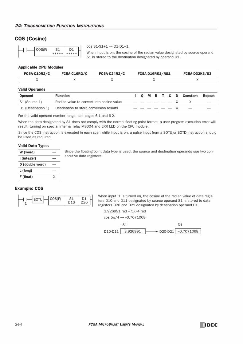
24: TRIGONOMETRIC FUNCTION INSTRUCTIONS
COS (Cosine)
Applicable CPU Modules
Valid Operands
For the valid operand number range, see pages 6-1 and 6-2.
When the data designated by S1 does not comply with the normal floating-point format, a user program execution error will result, turning on special internal relay M8004 and ERR LED on the CPU module.
Since the COS instruction is executed in each scan while input is on, a pulse input from a SOTU or SOTD instruction should be used as required.
Valid Data Types
Example: COS
FC5A-C10R2/C FC5A-C16R2/C FC5A-C24R2/C FC5A-D16RK1/RS1 FC5A-D32K3/S3
X X X X X
Operand Function I Q M R T C D Constant Repeat
S1 (Source 1) Radian value to convert into cosine value — — — — — — X X —
D1 (Destination 1) Destination to store conversion results — — — — — — X — —
W (word) —
I (integer) —
D (double word) —
L (long) —
F (float) X
cos S1·S1+1 → D1·D1+1
When input is on, the cosine of the radian value designated by source operand S1 is stored to the destination designated by operand D1.
COS(F) S1*****
D1*****
Since the floating point data type is used, the source and destination operands use two con-secutive data registers.
I1S1
D10COS(F) D1
D20
When input I1 is turned on, the cosine of the radian value of data regis-ters D10 and D11 designated by source operand S1 is stored to data registers D20 and D21 designated by destination operand D1.
3.926991 rad = 5π/4 rad
cos 5π/4 → –0.7071068
D1S1
3.926991D10·D11 –0.7071068D20·D21
SOTU
24-4 FC5A MICROSMART USER’S MANUAL

24: TRIGONOMETRIC FUNCTION INSTRUCTIONS
TAN (Tangent)
Applicable CPU Modules
Valid Operands
For the valid operand number range, see pages 6-1 and 6-2.
When the conversion result is not within the range between –3.402823 × 1038 and –1.175495 × 10–38 or between 1.175495 × 10–38 and 3.402823 × 1038, special internal relay M8003 (carry or borrow) is turned on except when the con-version result is 0. When the conversion result is below –3.402823 × 1038 or over 3.402823 × 1038, causing an overflow, the destination operand designated by D1 stores a value of minus or plus infinity.
When the data designated by S1 does not comply with the normal floating-point format, a user program execution error will result, turning on special internal relay M8004 and ERR LED on the CPU module.
Since the TAN instruction is executed in each scan while input is on, a pulse input from a SOTU or SOTD instruction should be used as required.
Valid Data Types
Example: TAN
FC5A-C10R2/C FC5A-C16R2/C FC5A-C24R2/C FC5A-D16RK1/RS1 FC5A-D32K3/S3
X X X X X
Operand Function I Q M R T C D Constant Repeat
S1 (Source 1) Radian value to convert into tangent value — — — — — — X X —
D1 (Destination 1) Destination to store conversion results — — — — — — X — —
W (word) —
I (integer) —
D (double word) —
L (long) —
F (float) X
tan S1·S1+1 → D1·D1+1
When input is on, the tangent of the radian value designated by source operand S1 is stored to the destination designated by operand D1.
TAN(F) S1*****
D1*****
0
–1.175495×10–38
M8003 1 1
1.175495×10–380–3.402823×1038
0
Execution Result
1
Overflow
0 1
3.402823×1038
OverflowNot Zero
Since the floating point data type is used, the source and destination operands use two con-secutive data registers.
I1S1
D10TAN(F) D1
D20
When input I1 is turned on, the tangent of the radian value of data regis-ters D10 and D11 designated by source operand S1 is stored to data registers D20 and D21 designated by destination operand D1.
3.926991 rad = 5π/4 rad
tan 5π/4 → 1.000001
D1S1
3.926991D10·D11 1.000001D20·D21
SOTU
FC5A MICROSMART USER’S MANUAL 24-5

24: TRIGONOMETRIC FUNCTION INSTRUCTIONS
ASIN (Arc Sine)
Applicable CPU Modules
Valid Operands
For the valid operand number range, see pages 6-1 and 6-2.
When the data designated by source operand S1 is not within the range between –1.0 and 1.0 or does not comply with the normal floating-point format, a user program execution error will result, turning on special internal relay M8004 and ERR LED on the CPU module.
Since the ASIN instruction is executed in each scan while input is on, a pulse input from a SOTU or SOTD instruction should be used as required.
Valid Data Types
Example: ASIN
FC5A-C10R2/C FC5A-C16R2/C FC5A-C24R2/C FC5A-D16RK1/RS1 FC5A-D32K3/S3
X X X X X
Operand Function I Q M R T C D Constant Repeat
S1 (Source 1) Arc sine value to convert into radian — — — — — — X X —
D1 (Destination 1) Destination to store conversion results — — — — — — X — —
W (word) —
I (integer) —
D (double word) —
L (long) —
F (float) X
asin S1·S1+1 → D1·D1+1 rad
When input is on, the arc sine of the value designated by source operand S1 is stored in radians to the destination designated by operand D1.
The S1·S1+1 value must be within the following range:
If the S1·S1+1 value is not within this range, an indefinite value is stored to D1·D1+1.
–1.0 ≤ S1·S1+1 ≤ 1.0
ASIN(F) S1*****
D1*****
Since the floating point data type is used, the source and destination operands use two con-secutive data registers.
I1S1
D10ASIN(F) D1
D20
When input I1 is turned on, the arc sine of the value of data registers D10 and D11 designated by source operand S1 is stored to data regis-ters D20 and D21 designated by destination operand D1.
asin –0.7071069 → –0.7853982 rad
–0.7853982 rad = –π/4 rad
D1S1
–0.7071069D10·D11 –0.7853982D20·D21
SOTU
24-6 FC5A MICROSMART USER’S MANUAL

24: TRIGONOMETRIC FUNCTION INSTRUCTIONS
ACOS (Arc Cosine)
Applicable CPU Modules
Valid Operands
For the valid operand number range, see pages 6-1 and 6-2.
When the data designated by source operand S1 is not within the range between –1.0 and 1.0 or does not comply with the normal floating-point format, a user program execution error will result, turning on special internal relay M8004 and ERR LED on the CPU module.
Since the ACOS instruction is executed in each scan while input is on, a pulse input from a SOTU or SOTD instruction should be used as required.
Valid Data Types
Example: ACOS
FC5A-C10R2/C FC5A-C16R2/C FC5A-C24R2/C FC5A-D16RK1/RS1 FC5A-D32K3/S3
X X X X X
Operand Function I Q M R T C D Constant Repeat
S1 (Source 1) Arc cosine value to convert into radian — — — — — — X X —
D1 (Destination 1) Destination to store conversion results — — — — — — X — —
W (word) —
I (integer) —
D (double word) —
L (long) —
F (float) X
acos S1·S1+1 → D1·D1+1 rad
When input is on, the arc cosine of the value designated by source operand S1 is stored in radians to the destination designated by operand D1.
The S1·S1+1 value must be within the following range:
If the S1·S1+1 value is not within this range, an indefinite value is stored to D1·D1+1.
–1.0 ≤ S1·S1+1 ≤ 1.0
ACOS(F) S1*****
D1*****
Since the floating point data type is used, the source and destination operands use two con-secutive data registers.
I1S1
D10ACOS(F) D1
D20
When input I1 is turned on, the arc cosine of the value of data registers D10 and D11 designated by source operand S1 is stored to data regis-ters D20 and D21 designated by destination operand D1.
acos –0.7071068 → 2.356195 rad
2.356195 rad = 3π/4 rad
D1S1
–0.7071068D10·D11 2.356195D20·D21
SOTU
FC5A MICROSMART USER’S MANUAL 24-7

24: TRIGONOMETRIC FUNCTION INSTRUCTIONS
ATAN (Arc Tangent)
Applicable CPU Modules
Valid Operands
For the valid operand number range, see pages 6-1 and 6-2.
When the data designated by source operand S1 does not comply with the normal floating-point format, a user program exe-cution error will result, turning on special internal relay M8004 and ERR LED on the CPU module.
Since the ATAN instruction is executed in each scan while input is on, a pulse input from a SOTU or SOTD instruction should be used as required.
Valid Data Types
Example: ATAN
FC5A-C10R2/C FC5A-C16R2/C FC5A-C24R2/C FC5A-D16RK1/RS1 FC5A-D32K3/S3
X X X X X
Operand Function I Q M R T C D Constant Repeat
S1 (Source 1) Arc tangent value to convert into radian — — — — — — X X —
D1 (Destination 1) Destination to store conversion results — — — — — — X — —
W (word) —
I (integer) —
D (double word) —
L (long) —
F (float) X
atan S1·S1+1 → D1·D1+1 rad
When input is on, the arc tangent of the value designated by source operand S1 is stored in radians to the destination designated by operand D1.
ATAN(F) S1*****
D1*****
Since the floating point data type is used, the source and destination operands use two con-secutive data registers.
I1S1
D10ATAN(F) D1
D20
When input I1 is turned on, the arc tangent of the value of data registers D10 and D11 designated by source operand S1 is stored to data regis-ters D20 and D21 designated by destination operand D1.
atan 0.4142136 → 0.3926992 rad
0.3926992 rad = π/8 rad
D1S1
0.4142136D10·D11 0.3926992D20·D21
SOTU
24-8 FC5A MICROSMART USER’S MANUAL

25: LOGARITHM / POWER INSTRUCTIONS
IntroductionThis chapter describes logarithm and power instructions which are used to calculate logarithm or powered values of source operands.
LOGE (Natural Logarithm)
Applicable CPU Modules
Valid Operands
For the valid operand number range, see pages 6-1 and 6-2.
When the data designated by source operand S1 is less than or equal to 0 or does not comply with the normal floating-point format, a user program execution error will result, turning on special internal relay M8004 and ERR LED on the CPU module.
Since the LOGE instruction is executed in each scan while input is on, a pulse input from a SOTU or SOTD instruction should be used as required.
Valid Data Types
Example: LOGE
FC5A-C10R2/C FC5A-C16R2/C FC5A-C24R2/C FC5A-D16RK1/RS1 FC5A-D32K3/S3
X X X X X
Operand Function I Q M R T C D Constant Repeat
S1 (Source 1) Binary data to convert into natural logarithm — — — — — — X X —
D1 (Destination 1) Destination to store conversion results — — — — — — X — —
W (word) —
I (integer) —
D (double word) —
L (long) —
F (float) X
loge S1·S1+1 → D1·D1+1
When input is on, the natural logarithm of the binary data designated by source operand S1 is stored to the destination designated by operand D1.
LOGE(F) S1*****
D1*****
Since the floating point data type is used, the source and destination operands use two consec-utive data registers.
I1S1
D10LOGE(F) D1
D20
When input I1 is on, the natural logarithm of the binary data of data reg-isters D10 and D11 designated by source operand S1 is stored to data registers D20 and D21 designated by destination operand D1.
loge 86 → 4.454347
D1S1
86.0D10·D11 4.454347D20·D21
SOTU
FC5A MICROSMART USER’S MANUAL 25-1

25: LOGARITHM / POWER INSTRUCTIONS
LOG10 (Common Logarithm)
Applicable CPU Modules
Valid Operands
For the valid operand number range, see pages 6-1 and 6-2.
When the data designated by source operand S1 is less than or equal to 0 or does not comply with the normal floating-point format, a user program execution error will result, turning on special internal relay M8004 and ERR LED on the CPU module.
Since the LOG10 instruction is executed in each scan while input is on, a pulse input from a SOTU or SOTD instruction should be used as required.
Valid Data Types
Example: LOG10
FC5A-C10R2/C FC5A-C16R2/C FC5A-C24R2/C FC5A-D16RK1/RS1 FC5A-D32K3/S3
X X X X X
Operand Function I Q M R T C D Constant Repeat
S1 (Source 1) Binary data to convert into common logarithm — — — — — — X X —
D1 (Destination 1) Destination to store conversion results — — — — — — X — —
W (word) —
I (integer) —
D (double word) —
L (long) —
F (float) X
log10 S1·S1+1 → D1·D1+1
When input is on, the common logarithm of the binary data designated by source operand S1 is stored to the destination designated by operand D1.
LOG10(F) S1*****
D1*****
Since the floating point data type is used, the source and destination operands use two consec-utive data registers.
I1S1
D10LOG10(F) D1
D20
When input I1 is on, the common logarithm of the binary data of data registers D10 and D11 designated by source operand S1 is stored to data registers D20 and D21 designated by destination operand D1.
log10 0.0000278 → –4.555955
D1S1
0.0000278D10·D11 –4.555955D20·D21
SOTU
25-2 FC5A MICROSMART USER’S MANUAL

25: LOGARITHM / POWER INSTRUCTIONS
EXP (Exponent)
Applicable CPU Modules
Valid Operands
For the valid operand number range, see pages 6-1 and 6-2.
When the operation result is not within the range between –3.402823 × 1038 and –1.175495 × 10–38 or between 1.175495 × 10–38 and 3.402823 × 1038, special internal relay M8003 (carry or borrow) is turned on except when the result is 0.
When the operation result is between –1.175495 × 10–38 and 1.175495 × 10–38, the destination operand designated by D1 stores 0. When the operation result is less than –3.402823 × 1038 or larger than 3.402823 × 1038, causing an overflow, the destination operand designated by D1 stores a value of minus or plus infinity.
When the data designated by source operand S1 does not comply with the normal floating-point format, a user program exe-cution error will result, turning on special internal relay M8004 and ERR LED on the CPU module.
Since the EXP instruction is executed in each scan while input is on, a pulse input from a SOTU or SOTD instruction should be used as required.
Valid Data Types
Example: EXP
FC5A-C10R2/C FC5A-C16R2/C FC5A-C24R2/C FC5A-D16RK1/RS1 FC5A-D32K3/S3
X X X X X
Operand Function I Q M R T C D Constant Repeat
S1 (Source 1) Binary data of exponent — — — — — — X X —
D1 (Destination 1) Destination to store results — — — — — — X — —
W (word) —
I (integer) —
D (double word) —
L (long) —
F (float) X
eS1·S1+1 → D1·D1+1
When input is on, e is raised to the power S1·S1+1 designated by source oper-and S1 and is stored to the destination designated by operand D1.
e (base of natural logarithm) = 2.7182818
EXP(F) S1*****
D1*****
Since the floating point data type is used, the source and destination operands use two consec-utive data registers.
I1S1
D10EXP(F) D1
D20
When input I1 is on, e is raised to the data of data registers D10 and D11 designated by source operand S1 and the operation result is stored to data registers D20 and D21 designated by destination operand D1.
e2 = 2.71828182 → 7.389056
D1S1
2.0D10·D11 7.389056D20·D21
SOTU
FC5A MICROSMART USER’S MANUAL 25-3

25: LOGARITHM / POWER INSTRUCTIONS
POW (Power)
Applicable CPU Modules
Valid Operands
For the valid operand number range, see pages 6-1 and 6-2.
When the operation result is not within the range between –3.402823 × 1038 and –1.175495 × 10–38 or between 1.175495 × 10–38 to 3.402823 × 1038, special internal relay M8003 (carry or borrow) is turned on, except when the result is 0.
When the operation result is between –1.175495 × 10–38 and 1.175495 × 10–38, the destination operand designated by D1 stores 0. When the operation result is less than –3.402823 × 1038 or greater than 3.402823 × 1038, causing an overflow, the destination operand designated by D1 stores a value of minus or plus infinity.
When one of the following conditions occurs, a user program execution error will result, turning on special internal relay M8004 and ERR LED on the CPU module.
• The data designated by source operand S1 is less than 0 and the data designated by source operand S2 is not an integer. • The data designated by source operand S1 is 0 and the data designated by source operand S2 is less than or equal to 0. • The data designated by source operand S1 or S2 does not comply with the normal floating-point format.
Since the POW instruction is executed in each scan while input is on, a pulse input from a SOTU or SOTD instruction should be used as required.
Valid Data Types
Example: POW
FC5A-C10R2/C FC5A-C16R2/C FC5A-C24R2/C FC5A-D16RK1/RS1 FC5A-D32K3/S3
X X X X X
Operand Function I Q M R T C D Constant Repeat
S1 (Source 1) Binary data of base — — — — — — X X —
S2 (Source 2) Binary data of exponent — — — — — — X X —
D1 (Destination 1) Destination to store results — — — — — — X — —
W (word) —
I (integer) —
D (double word) —
L (long) —
F (float) X
S1·S1+1S2·S2+1 → D1·D1+1
When input is on, binary data designated by source operand S1 is raised to the power S2·S2+1 designated by source operand S2 and the operation result is stored to the destination designated by operand D1.
POW(F) S1*****
D1*****
S2*****
Since the floating point data type is used, the source and destination operands use two consec-utive data registers.
I1S2
D20POW(F) D1
D30
When input I1 is on, the data of data registers D10 and D11 designated by source operand S1 is raised to the power D20·D20+1 designated by source operand S2 and the operation result is stored to data registers D30 and D31 designated by destination operand D1.
41.25 → 5.656856
S2S1
4.0D10·D11 1.25D20·D21
SOTU S1D10
D1
5.656856D30·D31
25-4 FC5A MICROSMART USER’S MANUAL

26: ANALOG I/O CONTROL
IntroductionThe MicroSmart provides analog I/O control capabilities of 12- through 16-bit resolution using analog I/O modules.
This chapter describes the system setup for using analog I/O modules, WindLDR programming procedures, data register allocation numbers for analog I/O modules, and application examples.
For hardware specifications of analog I/O modules, see page 2-44.
System SetupThe MicroSmart CPU module can be used with a maximum of seven expansion I/O modules, which include digital I/O modules and analog I/O modules.
Quantity of Applicable Analog I/O ModulesThe quantity of the analog I/O modules that can be connected to the MicroSmart CPU module depends on the model of the MicroSmart CPU modules as listed below:
System Setup Example
• Slot No.Indicates the position where the expansion module is mounted. The slot number starts with 1 next to the CPU module up to a maximum of 7.
Note: Analog I/O modules cannot be mounted to the right of the expansion interface module.
CPU ModuleAll-in-One Type CPU Module Slim Type CPU Module
FC5A-C10R2 FC5A-C10R2C
FC5A-C16R2 FC5A-C16R2C
FC5A-C24R2 FC5A-C24R2C
FC5A-D16RK1 FC5A-D16RS1
FC5A-D32K3 FC5A-D32S3
Quantity of Analog I/O Modules — — 4 7 7
Analog
Slot No.: 1 2 3 4
I/O
Expansion I/O Modules (7 maximum)
ModuleSlim Type
5 6 7
DigitalI/OModule
AnalogI/OModule
AnalogI/OModule
DigitalI/OModule
DigitalI/OModule
AnalogI/OModule
CPU Module
FC5A MICROSMART USER’S MANUAL 26-1
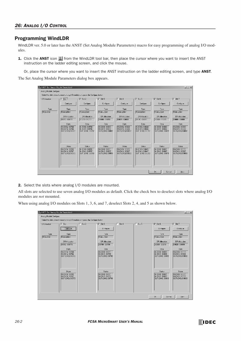
26: ANALOG I/O CONTROL
Programming WindLDRWindLDR ver. 5.0 or later has the ANST (Set Analog Module Parameters) macro for easy programming of analog I/O mod-ules.
1. Click the ANST icon from the WindLDR tool bar, then place the cursor where you want to insert the ANST instruction on the ladder editing screen, and click the mouse.
Or, place the cursor where you want to insert the ANST instruction on the ladder editing screen, and type ANST.
The Set Analog Module Parameters dialog box appears.
2. Select the slots where analog I/O modules are mounted.
All slots are selected to use seven analog I/O modules as default. Click the check box to deselect slots where analog I/O modules are not mounted.
When using analog I/O modules on Slots 1, 3, 6, and 7, deselect Slots 2, 4, and 5 as shown below.
26-2 FC5A MICROSMART USER’S MANUAL

26: ANALOG I/O CONTROL
3. Click the Configure button under the selected slots.
The Configure Parameters dialog box appears. All parameters for analog I/O control can be set in this dialog box. Avail-able parameters vary with the type of the analog I/O module.
4. Select the type of the analog I/O module.
Click on the right of the analog I/O module Type No., then a pull-down list shows eight available modules.
Depending on the selected analog I/O module, other parameters available for the selected module are shown.
In the Configure Parameters dialog box, parameters in white cells are selectable while gray cells indicate default parame-ters. In the white cells, optional values can be selected from a pull-down list or entered by typing required values.
Note for PID Instruction Source Operand S4 (process variable)
When using the PID instruction, specify the data register number shown under Data in the Configure Parameters dialog box as source operand S4 (process variable) of the PID instruction. The analog input data in the selected data register is used as the process variable of the PID instruction.
END Refresh Type Configure Parameters dialog box FC4A-L03A1 FC4A-L03AP1 FC4A-J2A1 FC4A-K1A1
Analog I/O Data (Note) Analog I/O Operating Status
Ladder Refresh Type Configure Parameters dialog box FC4A-J4CN1 FC4A-J8C1 FC4A-J8AT1 FC4A-K2C1
Analog I/O Data (Note) Analog I/O Operating Status
FC5A MICROSMART USER’S MANUAL 26-3

26: ANALOG I/O CONTROL
5. Select a DR allocation number (Ladder refresh type only).
6. Enter a filter value (Ladder refresh type analog input modules only).
The filter function is available for the FC4A-J4CN1, FC4A-J8C1, and FC4A-J8AT1 only. Filtering ensures smooth input of analog data into the CPU module.
7. Select a signal type for each channel.
Click on the right of the Signal Type field, then a pull-down list appears to show all available input or output signal types.
When you do not use any input or output signal, select the default value or Not used for the channel.
CPU Module DR Allocation
END Refresh Type FC4A-L03A1 FC4A-L03AP1 FC4A-J2A1 FC4A-K1A1
DR allocation starts with D760 as default, and the first DR number cannot be changed.One analog I/O module occupies 20 data registers. When a maximum of seven analog I/O modules are used, data registers D760 through D899 are used for analog I/O control.
Ladder Refresh Type FC4A-J4CN1 FC4A-J8C1 FC4A-J8AT1 FC4A-K2C1
The first data register can be selected as required. Enter the first DR number used for analog I/O control.One analog input module occupies a maximum of 65 data registers.One analog output module occupies 15 data registers.
Filter Value Description
0 or 1 Without filter function
2 to 255
The average of N pieces of analog input data is read as analog input data, where N is the designated filter value.
Analog I/O Module For unused channel, select
END Refresh TypeFC4A-L03A1, FC4A-J2A1 0 to 10V DC
FC4A-L03AP1 Type K
Ladder Refresh Type FC4A-J4CN1, FC4A-J8C1, FC4A-J8AT1, FC4A-K2C1 Not used
Ladder Refresh Type Configure Parameters dialog box
First Data Register No. Allocation range changes automatically.
Analog input data (Previous analog input data) (Filter value) (Current analog input data)+×(Filter value) 1+
--------------------------------------------------------------------------------------------------------------------------------------------------------------------------------------------=
26-4 FC5A MICROSMART USER’S MANUAL

26: ANALOG I/O CONTROL
8. Select a data type for each channel.
Click on the right of the Data Type field, then a pull-down list appears to show all available input or output data types.
9. Select a scale value (Ladder refresh type analog input modules only).
When Celsius or Fahrenheit is selected for thermocouple, resistance thermometer, or thermistor signal types on ladder refresh type analog input modules, the scale value can be selected from ×1, ×10, or ×100 depending on the selected signal type. Using this function, the analog input data can be multiplied to ensure precise control.
FC5A MICROSMART USER’S MANUAL 26-5

26: ANALOG I/O CONTROL
10. Select maximum and minimum values.
For analog input values, when Optional range is selected for the Data Type, designate the analog input data minimum and maximum values which can be –32,768 through 32,767.
In addition, when using resistance thermometers (Pt100, Pt1000, Ni100, or Ni1000) with the Celsius or Fahrenheit Data Type and the ×100 scale, select the analog input data minimum value from 0 or another value in the pull-down list. The maximum value is changed automatically according to the selected minimum value.
For analog output values, when Optional range is selected for the Data Type, designate the analog output data minimum and maximum values which can be –32,768 through 32,767.
11. View the data register numbers allocated to Data and Status.
12. Click the OK button to save changes and exit the Configure Parameter dialog box.
13. Repeat the same steps for other slots.
14. When finished, click the OK button to save changes and exit the Set Analog Module Parameters dialog box.
Parameter DR Allocation
Data
Analog I/O DataStores the digital data converted from an analog input signal or converted into an analog output signal.Designated as source operand S4 (process variable) of the PID instruction.
END Refresh TypeData registers are automatically allocated depending on the slot where the analog I/O module is mounted.
Ladder Refresh TypeData registers are automatically allocated depending on the number designated in the DR Allocation Num-ber field.
StatusAnalog I/O Operating StatusStores an analog I/O operating status code.See pages 26-13 and 26-15.
26-6 FC5A MICROSMART USER’S MANUAL

26: ANALOG I/O CONTROL
Analog I/O Control ParametersAvailable parameters for analog I/O control depend on the type of analog I/O modules as summarized in the following table. Designate the parameters in the Configure Parameters dialog box of the ANST macro as required by your applica-tion.
Parameter
Analog I/O Module Analog Input Module Analog Output Module
END Refresh Type Ladder Refresh Type END Ladder
FC4A-L03A1
FC4A-L03AP1
FC4A-J2A1
FC4A-J4CN1
FC4A-J8C1
FC4A-J8AT1
FC4A-K1A1
FC4A-K2C1
Analog Input Signal TypeX X X X X X — —
Page 26-11 Page 26-11 —
Analog Input Data TypeX X X X X X — —
Page 26-11 Page 26-11 —
Analog Input Data Minimum/Maximum Values
X X X X X X — —
Page 26-13 Page 26-13 —
Filter Value— — — X X X — —
— — Page 26-13 —
Thermistor Parameter— — — — — X — —
— — 26-13 —
Analog Input DataX X X X X X — —
Page 26-13 Page 26-13 —
Analog Input Operating Status
X X X X X X — —
Page 26-13 Page 26-13 —
Analog Output Signal TypeX X — — — — X X
Page 26-15 — Page 26-15
Analog Output Data TypeX X — — — — X X
Page 26-15 — Page 26-15
Analog Output Data Minimum/Maximum Values
X X — — — — X X
Page 26-15 — Page 26-15
Analog Output DataX X — — — — X X
Page 26-15 — Page 26-15
Analog Output Operating Status
X X — — — — X X
Page 26-15 — Page 26-15
FC5A MICROSMART USER’S MANUAL 26-7

26: ANALOG I/O CONTROL
Data Register Allocation Numbers for Analog I/O Modules Analog I/O modules are numbered from 1 through 7, in the order of increasing distance from the CPU module. Data regis-ters are allocated to each analog I/O module depending on the analog I/O module number. END refresh type analog I/O modules and ladder refresh type analog I/O modules have different data register allocation.
END Refresh Type Analog I/O ModulesEach END refresh type analog I/O module is automatically allocated 20 data registers to store parameters for controlling analog I/O operation, starting with D760 through D779 for analog I/O module No. 1, up to D880 through D899 for analog I/O module No. 7. When a maximum of seven analog I/O modules are not used, data registers allocated to the unused ana-log I/O module numbers can be used as ordinary data registers.
When a maximum of seven END refresh type analog I/O modules are mounted, data registers D760 through D899 are allocated to analog modules 1 through 7 as shown below. The ANST macro is used to program data registers for the analog I/O module configuration. The CPU module checks the analog I/O configuration only once when the CPU starts to run. If you have changed the parameter while the CPU is running, stop and restart the CPU to enable the new parameter.
The END refresh type analog I/O module number starts with 1 next to the CPU module up to a maximum of 7.
The run-time program download and test program download cannot be used to change analog I/O parameters.
Note: Data registers allocated to the unused analog I/O module numbers can be used as ordinary data registers.
Channel FunctionEND Refresh Type Analog I/O Module No.
R/W1 2 3 4 5 6 7
Analog InputCh 0
Analog input data D760 D780 D800 D820 D840 D860 D880 R
Analog input operating status D761 D781 D801 D821 D841 D861 D881 R
Analog input signal type D762 D782 D802 D822 D842 D862 D882 R/W
Analog input data type D763 D783 D803 D823 D843 D863 D883 R/W
Analog input data minimum value D764 D784 D804 D824 D844 D864 D884 R/W
Analog input data maximum value D765 D785 D805 D825 D845 D865 D885 R/W
Analog InputCh 1
Analog input data D766 D786 D806 D826 D846 D866 D886 R
Analog input operating status D767 D787 D807 D827 D847 D867 D887 R
Analog input signal type D768 D788 D808 D828 D848 D868 D888 R/W
Analog input data type D769 D789 D809 D829 D849 D869 D889 R/W
Analog input data minimum value D770 D790 D810 D830 D850 D870 D890 R/W
Analog input data maximum value D771 D791 D811 D831 D851 D871 D891 R/W
Analog Output
Analog output data D772 D792 D812 D832 D852 D872 D892 R/W
Analog output operating status D773 D793 D813 D833 D853 D873 D893 R
Analog output signal type D774 D794 D814 D834 D854 D874 D894 R/W
Analog output data type D775 D795 D815 D835 D855 D875 D895 R/W
Analog output data minimum value D776 D796 D816 D836 D856 D876 D896 R/W
Analog output data maximum value D777 D797 D817 D837 D857 D877 D897 R/W
– Reserved –D778 D798 D818 D838 D858 D878 D898 R/W
D779 D799 D819 D839 D859 D879 D899 R/W
26-8 FC5A MICROSMART USER’S MANUAL

26: ANALOG I/O CONTROL
Ladder Refresh Type Analog I/O ModulesWhen using a ladder refresh type analog input or output module, the first data register number can be designated in the ASNT macro dialog box. The quantity of required data registers depends on the model of the ladder refresh type analog input or output module.
Data register numbers and parameters are shown in the table below.
Ladder Refresh Type Analog Input Module Data Register Allocation (FC4A-J4CN1, FC4A-J8C1, and FC4A-J8AT1)
* Data registers for channels 4 through 7 are reserved on the FC4A-J4CN1.
Analog I/O Module FC4A-J4CN1 FC4A-J8C1 FC4A-J8AT1 FC4A-K2C1
Quantity of Data Registers for Analog I/O Operation 65 65 65 15
Data Register Number Offset
Data Size(word)
Parameter Channel Default R/W
+0 (Low Byte)1
Analog input signal type CH0 FFhR/W
+0 (High Byte) — Reserved — All channels 00h
+1 4 Analog input data configuration CH0 0 R/W
+5 1 Analog input signal typeCH1
00FFh R/W
+6 4 Analog input data configuration 0 R/W
+10 1 Analog input signal typeCH2
00FFh R/W
+11 4 Analog input data configuration 0 R/W
+15 1 Analog input signal typeCH3
00FFh R/W
+16 4 Analog input data configuration 0 R/W
+20 1 Analog input signal typeCH4 *
00FFh R/W
+21 4 Analog input data configuration 0 R/W
+25 1 Analog input signal typeCH5 *
00FFh R/W
+26 4 Analog input data configuration 0 R/W
+30 1 Analog input signal typeCH6 *
00FFh R/W
+31 4 Analog input data configuration 0 R/W
+35 1 Analog input signal typeCH7 *
00FFh R/W
+36 4 Analog input data configuration 0 R/W
+40 3 Thermistor parameters(FC4A-J8AT1 only)
CH0 to CH3 0 R/W
+43 3 CH4 to CH7 * 0 R/W
+46 1
Analog input data
CH0 — R
+47 1 CH1 — R
+48 1 CH2 — R
+49 1 CH3 — R
+50 1 CH4 * — R
+51 1 CH5 * — R
+52 1 CH6 * — R
+53 1 CH7 * — R
+54 1
Analog input operating status
CH0 — R
+55 1 CH1 — R
+56 1 CH2 — R
+57 1 CH3 — R
+58 1 CH4 * — R
+59 1 CH5 * — R
+60 1 CH6 * — R
+61 1 CH7 * — R
+62 3 — Reserved — All channels — R
FC5A MICROSMART USER’S MANUAL 26-9

26: ANALOG I/O CONTROL
Ladder Refresh Type Analog Output Module Data Register Allocation (FC4A-K2C1)
Data Register Number Offset
Data Size(word)
Parameter Channel Default R/W
+0 (Low Byte)1
Analog output signal type CH0 FFhR/W
+0 (High Byte) — Reserved — All channels 00h
+1 3 Analog output data configuration CH0 0 R/W
+4 1 Analog output signal typeCH1
00FFh R/W
+5 3 Analog output data configuration 0 R/W
+8 1Analog output data
CH0 0 R/W
+9 1 CH1 0 R/W
+10 1Analog output operating status
CH0 — R
+11 1 CH1 — R
+12 3 — Reserved — All channels — R
26-10 FC5A MICROSMART USER’S MANUAL

26: ANALOG I/O CONTROL
Analog Input ParametersAnalog input parameters include the analog input signal type, analog input data type, analog input minimum and maxi-mum values, filter value, thermistor parameter, analog input data, and analog input operating status. This section describes these parameters in detail.
Analog Input Signal TypeA total of 11 analog input signal types are available, depending on the analog I/O or analog input module. Select an analog input signal type for each analog input channel. When a channel is not used, select the default value or Not used for the channel.
Analog Input Data TypeA total of five analog input data types are available, depending on the analog I/O or analog input module. Select an analog input data type for each analog input channel.
Binary DataWhen Binary data is selected as an analog input data type, the analog input is linearly converted into digital data in the range described in the table below.
ParameterFC4A-
L03A1FC4A-
L03AP1FC4A-
J2A1FC4A-
J4CN1FC4A-
J8C1FC4A-
J8AT1
0 Voltage input (0 to 10V DC) X — X X X —
1 Current input (4 to 20 mA DC) X — X X X —
2 Type K thermocouple — X — X — —
3 Type J thermocouple — X — X — —
4 Type T thermocouple — X — X — —
5 Pt 100 resistance thermometer — X — X — —
6 Pt 1000 resistance thermometer — — — X — —
7 Ni 100 resistance thermometer — — — X — —
8 Ni 1000 resistance thermometer — — — X — —
9 NTC type thermistor — — — — — X
10 PTC type thermistor — — — — — X
255 Not used — — — X X X
ParameterFC4A-
L03A1FC4A-
L03AP1FC4A-
J2A1FC4A-
J4CN1FC4A-
J8C1FC4A-
J8AT1
0 Binary data X X X X X X
1 Optional range X X X X X X
2 Celsius — X — X — NTC only
3 Fahrenheit — X — X — NTC only
4 Resistance — — — — — X
Type No.FC4A-L03A1 FC4A-L03AP1 FC4A-J2A1
FC4A-J4CN1 FC4A-J8C1 FC4A-J8AT1
Analog Input Data 0 to 4095
Analog Input Signal Type Analog Input DataVoltage/Current: 0 to 50,000 Thermocouple: 0 to 50,000 Pt100, Ni100: 0 to 6,000 Pt1000, Ni1000: 0 to 60,000
0 to 50000 0 to 4000
FC5A MICROSMART USER’S MANUAL 26-11

26: ANALOG I/O CONTROL
Optional RangeWhen Optional range is selected as an analog input data type, the analog input is linearly converted into digital data in the range between the minimum and maximum values designated in the Configure Parameters dialog box.
Celsius and FahrenheitWhen Celsius or Fahrenheit is selected as an analog input data type, the analog input data range depends on the analog input signal type, scale value, and the type of the analog input module, FC4A-L03AP1, FC4A-J4CN1, and FC4A-J8AT1.
• FC4A-L03AP1
• FC4A-J4CN1
• FC4A-J8AT1
ResistanceWhen Resistance is selected as an analog input data type, the analog input is linearly converted into digital data in the range described in the table below. This option is available only when NTC or PTC type thermistor is selected for the FC4A-J8AT1.
• FC4A-J8AT1
Type No. FC4A-L03A1 FC4A-L03AP1 FC4A-J2A1 FC4A-J4CN1 FC4A-J8C1 FC4A-J8AT1
Analog Input Data Analog input data minimum value to maximum value (–32768 to 32767)
Analog Input Signal TypeCelsius Fahrenheit
Temperature (°C) Analog Input Data Temperature (°F) Analog Input Data
Type K thermocouple 0 to 1300 0 to 13000 32 to 2372 320 to 23720
Type J thermocouple 0 to 1200 0 to 12000 32 to 2192 320 to 21920
Type T thermocouple 0 to 400 0 to 4000 32 to 752 320 to 7520
Pt100 resistance thermometer –100.0 to 500.0 –1000 to 5000 –148.0 to 932.0 –1480 to 9320
Analog Input Signal Type
ScaleCelsius Fahrenheit
Temperature (°C) Analog Input Data Temperature (°F) Analog Input Data
Type K thermocouple ×1 0 to 1300 0 to 1300 32 to 2372 32 to 2372
×10 0.0 to 1300.0 0 to 13000 32.0 to 2372.0 320 to 23720
Type J thermocouple ×1 0 to 1200 0 to 1200 32 to 2192 32 to 2192
×10 0.0 to 1200.0 0 to 12000 32.0 to 2192.0 320 to 21920
Type T thermocouple ×1 0 to 400 0 to 400 32 to 752 32 to 752
×10 0.0 to 400.0 0 to 4000 32.0 to 752.0 320 to 7520
Pt100, Pt1000 resistance thermometer
×1 –100 to 500 –100 to 500 –148 to 932 –148 to 932
×10 –100.0 to 500.0 –1000 to 5000 –148.0 to 932.0 –1480 to 9320
×100 0.00 to 500.00
–100.00 to 327.67 0 to 50000
–10000 to 32767 0.00 to 655.35
–148.00 to 327.67 0 to 65535
–14800 to 32767
Ni100, Ni1000 resistance thermometer
×1 –60 to 180 –60 to 180 –76 to 356 –76 to 356
×10 –60.0 to 180.0 –600 to 1800 –76.0 to 356.0 –760 to 3560
×100 –60.00 to 180.00 –6000 to 18000 0.00 to 356.00
–76.00 to 327.67 0 to 35600
–7600 to 32767
Analog Input Signal Type
ScaleCelsius Fahrenheit
Temperature (°C) Analog Input Data Temperature (°F) Analog Input Data
NTC thermistor ×1 –50 to 150 –50 to 150 –58 to 302 –58 to 302
×10 –50.0 to 150.0 –500 to 1500 –58.0 to 302.0 –580 to 3020
Analog Input Signal TypeResistance
Resistance (Ω) Analog Input Data
NTC/PTC thermistor 0 to 100000 0 to 10000
26-12 FC5A MICROSMART USER’S MANUAL

26: ANALOG I/O CONTROL
Analog Input Minimum/Maximum ValuesFor analog input values, when Optional range is selected for the Data Type, designate the analog input data minimum and maximum values which can be –32,768 through 32,767.
In addition, when using resistance thermometers (Pt100, Pt1000, Ni100, or Ni1000) with the Celsius or Fahrenheit Data Type and the ×100 scale, select the analog input data minimum value from 0 or another value in the pull-down list. The maximum value is changed automatically according to the selected minimum value.
Filter ValueThe filter function is available for the ladder input type FC4A-J4CN1, FC4A-J8C1, and FC4A-J8AT1 only. Filtering ensures smooth input of analog data into the CPU module. For the filtering function of analog input signals, see page 26-4.
Valid values are 0 through 255.
Thermistor ParameterThermistor parameters are enabled when selecting NTC thermistor for the analog input type of the FC4A-J8AT1. The same parameters are specified for four channels: CH0 to CH3 and CH4 to CH7.
For NTC type thermistors, analog input data can be calculated from the following formula:
For PTC type thermistors, linearize the analog input data using the XYFS instruction.
Analog Input DataThe analog input signal is converted into a digital value within the range specified by the analog input data type and appli-cable parameters, and is stored to a data register allocated to analog input data. The analog input data register number is shown under Data in the Configure Parameters dialog box.
END Refresh TypeThe analog input signal is converted into a digital value and stored to a data register, such as D760 or D766, allocated to analog input channel 1 or 2 on analog module number 1 through 7 depending on the mounting position.
The analog input data stored in the allocated data register is updated whether the CPU module is running or stopped. When the CPU module is running, the update occurs at the END processing of every scan or 10 ms, whichever is longer. When the CPU module is stopped, the update occurs every 10 ms.
Ladder Refresh TypeThe analog input signal is converted into a digital value and stored to a data register determined by the data register num-ber selected in the Configure Parameters dialog box of the ANST macro. The analog input data stored in the allocated data register is updated when the RUNA instruction contained in the ANST macro is executed.
When a certain channel of a ladder refresh type analog input module is not used, data registers allocated to the unused channel will store indefinite values if the values are read out of the analog input module. Do not use the allocated data reg-isters for other purposes.
Only when the analog input status code is 0, the analog input data is assured. Make sure that a user program reads analog input data only when the analog input status code is 0.
Analog Input Operating StatusThe operating status of each analog input channel is stored to a data register allocated to analog input operating status. While the analog input is operating normally, the data register stores 0. The analog input operating status data register number is shown under Status in the Configure Parameters dialog box.
ChannelNTC Thermistor Parameters
(Values indicated on the thermistor)Valid Range
CH0 to CH3CH4 to CH7
R0: Thermistor resistance value at the absolute temperature 0 to 65535
T0: Absolute temperature –32768 to 32767
B: Thermistor B parameter 0 to 65535
Analog Input Data B T0×B T0 r R0⁄( )log×+-------------------------------------------------=
where, r = thermistor resistance (Ω)
FC5A MICROSMART USER’S MANUAL 26-13

26: ANALOG I/O CONTROL
END Refresh TypeThe operating status of each analog input channel is stored to a data register, such as D761 or D767, allocated to analog input channel 1 or 2 on analog module number 1 through 7 depending on the mounting position.
The analog input operating status data is updated whether the CPU module is running or stopped. When the CPU module is running, the update occurs at the END processing of every scan or 10 ms, whichever is longer. When the CPU module is stopped, the update occurs every 10 ms.
Ladder Refresh TypeThe operating status of each analog input channel is stored to a data register determined by the data register number selected in the Configure Parameters dialog box of the ANST macro.
Status Code Analog Input Operating Status (END refresh type)
0 Normal operation
1 Converting data (during the first data conversion after power-up)
2 Initializing
3 Invalid parameter or analog input channel not available on the installed analog module
4 Hardware failure (external power supply failure)
5 Incorrect wiring (input data over valid range)
6 Incorrect wiring (input data below valid range or current loop open)
Operating Status Bit Analog Input Operating Status (Ladder refresh type)
Bit 00
Operating status bitNormal operation
1 Initializing, changing configuration, hardware initialization error
Bit 10
Parameter bitParameter configuration normal
1 Parameter configuration error
Bit 20
External power supply bitExternal power supply normal
1 External power supply error
Bit 30
Maximum value over bitWithin the maximum value
1 Maximum value over error
Bit 40
Minimum value over bitWithin the minimum value
1 Minimum value under error
Bit 5 to Bit 15 0 Reserved Normal operation
26-14 FC5A MICROSMART USER’S MANUAL

26: ANALOG I/O CONTROL
Analog Output ParametersAnalog output parameters include the analog output signal type, analog output data type, analog output minimum and maximum values, analog output data, and analog output operating status. This section describes these parameters in detail.
Analog Output Signal TypeA total of three analog output signal types are available, depending on the analog I/O or analog output module. Select an analog output signal type for each analog output channel. When a channel is not used, select the default value or Not used for the channel.
Analog Output Data TypeA total of two analog output data types are available, depending on the analog I/O or analog output module. Select an ana-log output data type for each analog output channel.
Analog Output Minimum/Maximum ValuesFor analog output values, when Optional range is selected for the Data Type, designate the analog output data minimum and maximum values which can be –32,768 through 32,767.
Analog Output DataThe analog output data is converted into an analog output signal within the range specified by the analog output data type and applicable parameters. The analog output data register number is shown under Data in the Configure Parameters dia-log box.
END Refresh TypeThe analog output data stored in a data register, such as D772, is converted into an analog output signal of voltage output (0 to 10V DC) or current output (4 to 20 mA) as designated by the value stored in the data register allocated to analog out-put signal type, such as D774.
While the CPU module is running, the analog output data stored in the allocated data register is updated at the END pro-cessing of every scan or 10 ms, whichever is longer. While the CPU module is stopped, the analog output data remains at 0 or the designated analog output data minimum value, so the generated analog output signal remains at the minimum value of 0V DC or 4 mA DC.
Ladder Refresh TypeWhile the CPU module is running, the analog output data stored in the allocated data register is updated when the RUNA instruction contained in the ANST macro is executed. While the CPU module is stopped, the analog output data is not updated. But the analog output signal can be changed by using the STPA instruction. For details, see page 26-21.
Analog Output Operating StatusThe operating status of each analog output channel is stored to a data register allocated to analog output operating status. While the analog output is operating normally, the data register stores 0. The analog output operating status data register number is shown under Status in the Configure Parameters dialog box.
END Refresh TypeThe operating status of each analog output is stored to a data register, such as D773. While the analog output is operating normally, the data register stores 0. The analog output operating status data is updated whether the CPU module is running or stopped. The update occurs at the END processing of every scan or 10 ms, whichever is longer.
Parameter FC4A-L03A1 FC4A-L03AP1 FC4A-K1A1 FC4A-K2C1
0 Voltage input 0 to 10V DC –10 to +10V DC
1 Current input 4 to 20 mA DC
255 Not used — — — X
Parameter FC4A-L03A1 FC4A-L03AP1 FC4A-K1A1 FC4A-K2C1
0 Binary dataVoltage
0 to 4095–25000 to 25000
Current 0 to 50000
1 Optional rangeVoltage
Analog output data minimum value to maximum value (–32768 to 32767)Current
FC5A MICROSMART USER’S MANUAL 26-15
26: ANALOG I/O CONTROL
Ladder Refresh TypeThe operating status of each analog output channel is stored to a data register determined by the data register number selected in the Configure Parameters dialog box of the ANST macro.
Status Code Analog Output Operating Status (END refresh type)
0 Normal operation
1 (reserved)
2 Initializing
3 Invalid parameter or analog output channel not available on the installed analog module
4 Hardware failure (external power supply failure)
Operating Status Bit Analog Output Operating Status (Ladder refresh type)
Bit 00
Operating status bitNormal operation
1 Initializing, changing configuration, hardware initialization error
Bit 10
Parameter bitParameter configuration normal
1 Parameter configuration error
Bit 20
External power supply bitExternal power supply normal
1 External power supply error
Bit 30
Output data error bitOutput data normal
1 Output data range error
Bit 4 to Bit 15 0 Reserved Normal operation
26-16 FC5A MICROSMART USER’S MANUAL

26: ANALOG I/O CONTROL
Example: Analog I/OThe following example demonstrates a program of analog I/O control using an NTC thermistor. Two analog I/O modules are mounted in the slots shown below.
System Setup
OperationIn this example, the input value from the NTC thermistor is calibrated. When the temperature reaches the preset value, the output is turned off. The thermistor temperature is monitored on an analog meter.
Slot No.: 1 2 3
Slim Type CPU Module FC5A-D32S3
Analog Input Module (Thermistor) FC4A-J8AT1
Output Module (Tr. Source) FC4A-T08S1
ThermistorExternalDevice
Analog Meter
Calibrated voltage
Analog Output Module FC4A-K1A1
FC5A MICROSMART USER’S MANUAL 26-17

26: ANALOG I/O CONTROL
Wiring Diagram
FC4A-J8AT1 (Analog Input Module)
FC4A-T08S1 (8-point Transistor Source Output Module)
FC4A-K1A1 (Analog Output Module)
Terminal No. Channel24V
24V DC0V
NC —A
IN0BA
IN1BA
IN2B
AIN3
BA
IN4BA
IN5BA
IN6BA
IN7B
Fuse+–
24V DC
NTC Thermistor B
A
• Thermistor Specifications
Type No. NT731ATTD103K38J (KOA)
Type NTC
RO 10,000Ω
T0 298K (25°C)
B Parameter 3,800K
Terminal No. Output0 Q01 Q12 Q23 Q34 Q45 Q56 Q67 Q7
COM(+) COM(+)–V –V
Fuse+–
External Device
+IN
–IN
Terminal No. Channel+
24V DC–
+OUT
–NC
—NCNCNC
—NCNC
Fuse+–
24V DC
+ –
Analog Meter
V
26-18 FC5A MICROSMART USER’S MANUAL

26: ANALOG I/O CONTROL
WindLDR ProgrammingAnalog I/O modules are programmed using the ANST macro in WindLDR. Program the ANST macro as shown below.
• Analog Input Module FC4A-J8AT1 on Slot 1
Note: When CH4 through CH7 are not used, thermistor settings are not required.
DR Allocation Range Designation Description
D630 - D694 D630 Optional range allocation, 65 words
I/O Channel Item Designation Description
IN
CH0
Filter 10 Averages input values
Data Type Celsius Analog input range –50 to 150°C
Scale ×10 Analog input data –500 to 1500
CH1 Data Type Not used Unused channel
CH2 Data Type Not used Unused channel
CH3 Data Type Not used Unused channel
CH4 Data Type Not used Unused channel
CH5 Data Type Not used Unused channel
CH6 Data Type Not used Unused channel
CH7 Data Type Not used Unused channel
CH0 - CH3
Thermistor Type NTC NTC thermistor
R0 10,000 Resistance value at the absolute temperature = 10 kΩ
T0 298 Absolute temperature = 298K (25°C)
B 3,800 B parameter = 3,800K
FC5A MICROSMART USER’S MANUAL 26-19

26: ANALOG I/O CONTROL
• Analog Output Module FC4A-K1A1 on Slot 3
Ladder DiagramAs shown in the ladder diagram below, when initialize pulse special internal relay M8120 is used for the ANST macro in parallel with another instruction, load M8120 again for the other instruction.
Note: The above ladder diagram is only an example and should be modified as required.
DR Allocation Range Designation Description
D760 - D779 — Automatic range allocation, 20 words
I/O Channel Item Designation Description
OUT CH0Signal Type 0 to 10V DC Voltage output
Data Type Binary data 0 to 4095
M8120 is the initialize pulse special internal relay.
When the CPU starts to run, ANST stores parameters to data registers to configure analog I/O modules and Q30 is turned on.
When I0 is turned on, analog input data is moved from D676 to D1000.
The temperature is compared with the alarm tempera-ture of 100°C.
When the temperature is higher than 100°C, Q30 is turned off.
When the temperature is not higher than 100°C, Q30 is turned on.
Analog input data of –500 to +1500 is converted to 0 to 2000.
Analog input data of 0 to 2000 is converted to 0 to 4000.
Analog input data of 0 to 4000 is moved to D772 (ana-log output data) of the analog output module.
M8120
REPS1 –D676
D1 –D1000
MOV(I)
REPS1 –D1000
D1 –D772
MOV(W)
REPS1 –D676
D1 –M30
CMP>(I) S2 –1000
NO.1J8AT1
NO.3K1A1
ANST
Q30S
Q30R
Q30S
M30
M30
I0
REPS2 –500
D1 –D1000
S1 –D1000
ADD(I)
REPS2 –2
D1 –D1000
S1 –D1000
MUL(W)
M8120
26-20 FC5A MICROSMART USER’S MANUAL

26: ANALOG I/O CONTROL
Changing Analog Output While CPU is StoppedWhen using the FC4A-K2C1 analog output module, the analog output value can be changed while the CPU module is stopped. To change the analog output value, store a required output value to the memory addresses allocated to the analog output data.
Example: Memory Allocation of Ladder Refresh Type Analog Output Module FC4A-K2C1
STPA instruction when FC4A-K2C1 is mounted on slot 4
Ladder Diagram
Note: The above ladder diagram is only an example and should be modified as required.
Precautions for Programming ANST MacroWhen using the ANST macro, do not make a branch from the ladder line of the ANST macro.
Delete the branch from the ANST macro, and start another line by inserting a LOD instruction.
Memory Address(data address used for STPA)
Data Size(bytes)
R/W Parameter
+20 2 R/WAnalog Output Data
CH0
+22 2 R/W CH1
M8120 is the initialize pulse special internal relay.
MOV stores output values at the OFF state.
When the CPU stops, STPA updates the analog output value of the analog output module.
M8120REP2
S1 –0
D1 RD1400
MOV(I)
DATAD1400
SLOT4
STATUSD1500
BYTE4
ADDRESS20WRITE
STPA(I)
M8120NO.1J8AT1
ANST
Q1
Incorrect
M8120NO.1J8AT1
ANST
Q1M8120
Correct
FC5A MICROSMART USER’S MANUAL 26-21

26: ANALOG I/O CONTROL
26-22 FC5A MICROSMART USER’S MANUAL

27: DATA LINK COMMUNICATION
IntroductionThis chapter describes the data link communication function used to set up a distributed control system.
A data link communication system consists of one master station and a maximum of 31 slave stations, each station com-prising any all-in-one type or slim type CPU module. When the data link communication is enabled, the master station has 12 data registers assigned for each slave station, and each slave station has 12 data registers for communication with the master station. Using these data registers, the master station can send and receive data of 6 data registers to and from each slave station. No particular program is required for sending or receiving data in the data link communication system.
Data link communication proceeds independently of the user program execution, and the data registers for the data link communication are updated at the END processing.
When data of inputs, outputs, internal relays, timers, counters, or shift registers are moved to data registers using the move instructions in the user program, these data can also be exchanged between the master and slave stations.
The FC4A MicroSmart (except all-in-one 10-I/O type CPU module), OpenNet Controller, MICRO3, MICRO3C, and FA-3S series PLCs can also be connected to the data link communication system.
Data Link Specifications
Electric Specifications Compliance with EIA-RS485
Baud Rate 19,200, 38,400, 57,600 bps
Synchronization
Start-stop synchronizationStart bit: 1 Data bits: 7 Parity: Even Stop bit: 1
Communication Cable Shielded twisted pair cable, core wire 0.3 mm2
Maximum Cable Length 200m (656 feet) total
Maximum Slave Stations 31 slave stations
Transmit/Receive DataTransmit data: 186 words maximum, Receive data: 186 words maximum0 through 6 words each for transmission and receiving per slave station
Special Internal RelayM8005-M8007: communication control and error M8080-M8116: communication completion for each slave station M8117: communication completion for all slave stations
Data Register D900-D1271: transmit/receive data
Special Data RegisterD8069-D8099: communication error code D8100: data link slave station number
Master Station Slave Station 1 Slave Station 31
FC5A MICROSMART USER’S MANUAL 27-1

27: DATA LINK COMMUNICATION
Data Link System SetupTo set up a data link system, install the RS485 communication adapter (FC4A-PC3) to the port 2 connector on the all-in-one type CPU module.
When using the slim type CPU module, mount the RS485 communication module (FC4A-HPC3) next to the CPU module.
When using the optional HMI module (FC4A-PH1) with the slim type CPU module, install the RS485 communication adapter (FC4A-PC3) to the port 2 connector on the HMI base module (FC4A-HPH1).
Connect the RS485 terminals A, B, and SG on every CPU module using a shielded twisted pair cable as shown below. The total length of the cable for the data link system can be extended up to 200 meters (656 feet).
A B SG
Cable Cable
A B SG
Master Station Slave Station 1
Slave Station 2Slave Station 31
RS485 Communication Adapter FC4A-PC3
on Port 2 Connector
HMI Base Module FC4A-HPH1
All-in-One Type CPU Module
Slim Type CPU Module
Shielded twisted pair cable 200 meters (656 feet) maximumCore wire 0.3mm2
RS485 Communication Module FC4A-HPC3
RS485 Communication Adapter FC4A-PC3
on Port 2 Connector
27-2 FC5A MICROSMART USER’S MANUAL

27: DATA LINK COMMUNICATION
Data Register Allocation for Transmit/Receive DataThe master station has 12 data registers assigned for data communication with each slave station. Each slave station has 12 data registers assigned for data communication with the master station. When data is set in data registers at the master sta-tion assigned for data link communication, the data is sent to the corresponding data registers at a slave station. When data is set in data registers at a slave station assigned for data link communication, the data is sent to the corresponding data registers at the master station.
Master Station
If any slave stations are not connected, master station data registers which are assigned to the vacant slave stations can be used as ordinary data registers.
Slave Station
Slave station data registers D912 through D1271 can be used as ordinary data registers.
Slave Station Number
Data Register Transmit/Receive DataSlave
Station Number
Data Register Transmit/Receive Data
Slave 1D900-D905 Transmit data to slave 1
Slave 17D1092-D1097 Transmit data to slave 17
D906-D911 Receive data from slave 1 D1098-D1103 Receive data from slave 17
Slave 2D912-D917 Transmit data to slave 2
Slave 18D1104-D1109 Transmit data to slave 18
D918-D923 Receive data from slave 2 D1110-D1115 Receive data from slave 18
Slave 3D924-D929 Transmit data to slave 3
Slave 19D1116-D1121 Transmit data to slave 19
D930-D935 Receive data from slave 3 D1122-D1127 Receive data from slave 19
Slave 4D936-D941 Transmit data to slave 4
Slave 20D1128-D1133 Transmit data to slave 20
D942-D947 Receive data from slave 4 D1134-D1139 Receive data from slave 20
Slave 5D948-D953 Transmit data to slave 5
Slave 21D1140-D1145 Transmit data to slave 21
D954-D959 Receive data from slave 5 D1146-D1151 Receive data from slave 21
Slave 6D960-D965 Transmit data to slave 6
Slave 22D1152-D1157 Transmit data to slave 22
D966-D971 Receive data from slave 6 D1158-D1163 Receive data from slave 22
Slave 7D972-D977 Transmit data to slave 7
Slave 23D1164-D1169 Transmit data to slave 23
D978-D983 Receive data from slave 7 D1170-D1175 Receive data from slave 23
Slave 8D984-D989 Transmit data to slave 8
Slave 24D1176-D1181 Transmit data to slave 24
D990-D995 Receive data from slave 8 D1182-D1187 Receive data from slave 24
Slave 9D996-D1001 Transmit data to slave 9
Slave 25D1188-D1193 Transmit data to slave 25
D1002-D1007 Receive data from slave 9 D1194-D1199 Receive data from slave 25
Slave 10D1008-D1013 Transmit data to slave 10
Slave 26D1200-D1205 Transmit data to slave 26
D1014-D1019 Receive data from slave 10 D1206-D1211 Receive data from slave 26
Slave 11D1020-D1025 Transmit data to slave 11
Slave 27D1212-D1217 Transmit data to slave 27
D1026-D1031 Receive data from slave 11 D1218-D1223 Receive data from slave 27
Slave 12D1032-D1037 Transmit data to slave 12
Slave 28D1224-D1229 Transmit data to slave 28
D1038-D1043 Receive data from slave 12 D1230-D1235 Receive data from slave 28
Slave 13D1044-D1049 Transmit data to slave 13
Slave 29D1236-D1241 Transmit data to slave 29
D1050-D1055 Receive data from slave 13 D1242-D1247 Receive data from slave 29
Slave 14D1056-D1061 Transmit data to slave 14
Slave 30D1248-D1253 Transmit data to slave 30
D1062-D1067 Receive data from slave 14 D1254-D1259 Receive data from slave 30
Slave 15D1068-D1073 Transmit data to slave 15
Slave 31D1260-D1265 Transmit data to slave 31
D1074-D1079 Receive data from slave 15 D1266-D1271 Receive data from slave 31
Slave 16D1080-D1085 Transmit data to slave 16
—D1086-D1091 Receive data from slave 16
Data Data Register Transmit/Receive Data
Slave Station DataD900-D905 Transmit data to master stationD906-D911 Receive data from master station
FC5A MICROSMART USER’S MANUAL 27-3

27: DATA LINK COMMUNICATION
Special Data Registers for Data Link Communication ErrorIn addition to data registers assigned for data communication, the master station has 31 special data registers and each slave station has one special data register to store data link communication error codes. If any communication error occurs in the data link system, communication error codes are set to a corresponding data register for link communication error at the master station and to data register D8069 at the slave station. For details of link communication error codes, see below.
If a communication error occurs in the data link communication system, the data is resent two times. If the error still exists after three attempts, then the error code is set to the data registers for data link communication error. Since the error code is not communicated between the master and slave stations, error codes must be cleared individually.
Master Station
If any slave stations are not connected, master station data registers which are assigned to the vacant slave stations can be used as ordinary data registers.
Slave Station
Note: Slave station data registers D8070 through D8099 can be used as ordinary data registers.
Data Link Communication Error CodeThe data link error code is stored in the special data register allocated to indicate a communication error in the data link system. When this error occurs, special internal relay M8005 (communication error) is also turned on at both master and slave stations. The detailed information of general errors can be viewed using WindLDR. Select Online > Monitor, then select Online > PLC Status > Error Status: Details. See page 32-2.
When more than one error is detected in the data link system, the total of error codes is indicated. For example, when framing error (error code 2h) and BCC error (error code 10h) are found, error code 12h (18) is stored.
Special Data Register
Data Link Communication Error DataSpecial Data
RegisterData Link Communication Error Data
D8069 Slave station 1 communication error D8085 Slave station 17 communication errorD8070 Slave station 2 communication error D8086 Slave station 18 communication errorD8071 Slave station 3 communication error D8087 Slave station 19 communication errorD8072 Slave station 4 communication error D8088 Slave station 20 communication errorD8073 Slave station 5 communication error D8089 Slave station 21 communication errorD8074 Slave station 6 communication error D8090 Slave station 22 communication errorD8075 Slave station 7 communication error D8091 Slave station 23 communication errorD8076 Slave station 8 communication error D8092 Slave station 24 communication errorD8077 Slave station 9 communication error D8093 Slave station 25 communication errorD8078 Slave station 10 communication error D8094 Slave station 26 communication errorD8079 Slave station 11 communication error D8095 Slave station 27 communication errorD8080 Slave station 12 communication error D8096 Slave station 28 communication errorD8081 Slave station 13 communication error D8097 Slave station 29 communication errorD8082 Slave station 14 communication error D8098 Slave station 30 communication errorD8083 Slave station 15 communication error D8099 Slave station 31 communication errorD8084 Slave station 16 communication error — —
Special Data Register Data Link Communication Error DataD8069 Slave station communication error
Error Code Error Details1h (1) Overrun error (data is received when the receive data registers are full)2h (2) Framing error (failure to detect start or stop bit)4h (4) Parity error (an error was found by the parity check)8h (8) Receive timeout (line disconnection)
10h (16) BCC (block check character) error (disparity with data received up to BCC)20h (32) Retry cycle over (error occurred in all 3 trials of communication)40h (64) I/O definition quantity error (discrepancy of transmit/receive station number or data quantity)
27-4 FC5A MICROSMART USER’S MANUAL

27: DATA LINK COMMUNICATION
Data Link Communication between Master and Slave StationsThe master station has 6 data registers assigned to transmit data to a slave station and 6 data registers assigned to receive data from a slave station. The quantity of data registers for data link can be selected from 0 through 6 using WindLDR. The following examples illustrate how data is exchanged between the master and slave stations when 2 or 6 data registers are used for data link communication with each of 31 slave stations.
Example 1: Transmit Data 2 Words and Receive Data 2 Words
Example 2: Transmit Data 6 Words and Receive Data 6 Words
Master Station
D8069 Communication Error
D900 - D901 Transmit Data
D906 - D907 Receive Data
D8070 Communication Error
D912 - D913 Transmit Data
D918 - D919 Receive Data
D8071 Communication Error
D924 - D925 Transmit Data
D930 - D931 Receive Data
D8072 Communication Error
D936 - D937 Transmit Data
D942 - D943 Receive Data
D8098 Communication Error
D1248 - D1249 Transmit Data
D1254 - D1255 Receive Data
D8099 Communication Error
D1260 - D1261 Transmit Data
D1266 - D1267 Receive Data
Slave Stations
D8069 Communication Error
Slave Station 1D900 - D901 Transmit Data
D906 - D907 Receive Data
D8069 Communication Error
Slave Station 2D900 - D901 Transmit Data
D906 - D907 Receive Data
D8069 Communication Error
Slave Station 3D900 - D901 Transmit Data
D906 - D907 Receive Data
D8069 Communication Error
Slave Station 4D900 - D901 Transmit Data
D906 - D907 Receive Data
D8069 Communication Error
Slave Station 30D900 - D901 Transmit Data
D906 - D907 Receive Data
D8069 Communication Error
Slave Station 31D900 - D901 Transmit Data
D906 - D907 Receive Data
Master Station
D8069 Communication Error
D900 - D905 Transmit Data
D906 - D911 Receive Data
D8070 Communication Error
D912 - D917 Transmit Data
D918 - D923 Receive Data
D8071 Communication Error
D924 - D929 Transmit Data
D930 - D935 Receive Data
D8072 Communication Error
D936 - D941 Transmit Data
D942 - D947 Receive Data
D8098 Communication Error
D1248 - D1253 Transmit Data
D1254 - D1259 Receive Data
D8099 Communication Error
D1260 - D1265 Transmit Data
D1266 - D1271 Receive Data
Slave Stations
D8069 Communication Error
Slave Station 1D900 - D905 Transmit Data
D906 - D911 Receive Data
D8069 Communication Error
Slave Station 2D900 - D905 Transmit Data
D906 - D911 Receive Data
D8069 Communication Error
Slave Station 3D900 - D905 Transmit Data
D906 - D911 Receive Data
D8069 Communication Error
Slave Station 4D900 - D905 Transmit Data
D906 - D911 Receive Data
D8069 Communication Error
Slave Station 30D900 - D905 Transmit Data
D906 - D911 Receive Data
D8069 Communication Error
Slave Station 31D900 - D905 Transmit Data
D906 - D911 Receive Data
FC5A MICROSMART USER’S MANUAL 27-5

27: DATA LINK COMMUNICATION
Special Internal Relays for Data Link CommunicationSpecial internal relays M8005 through M8007 and M8080 through M8117 are assigned for the data link communication.
M8005 Data Link Communication Error
When an error occurs during communication in the data link system, M8005 turns on. The M8005 status is maintained when the error is cleared and remains on until M8005 is reset using WindLDR or until the CPU is turned off. The cause of the data link communication error can be checked using Online > Monitor, followed by Online > PLC Status > Error Sta-tus: Details. See page 27-4.
M8006 Data Link Communication Prohibit Flag (Master Station)
When M8006 at the master station is turned on in the data link system, data link communication is stopped. When M8006 is turned off, data link communication resumes. The M8006 status is maintained when the CPU is turned off and remains on until M8006 is reset using WindLDR.
When M8006 is on at the master station, M8007 is turned on at slave stations in the data link system.
M8007 Data Link Communication Initialize Flag (Master Station) Data Link Communication Stop Flag (Slave Station)
M8007 has a different function at the master or slave station of the data link communication system.
Master station: Data link communication initialize flagWhen M8007 at the master station is turned on during operation, the link configuration is checked to initialize the data link system. When a slave station is powered up after the master station, turn M8007 on to initialize the data link system. After a data link system setup is changed, M8007 must also be turned on to ensure correct communication.
Slave station: Data link communication stop flagWhen a slave station does not receive communication data from the master station for 10 seconds or more in the data link system, M8007 turns on. When a slave station does not receive data in 10 seconds after initializing the data link system, M8007 also turns on at the slave station. When the slave station receives correct communication data, M8007 turns off.
M8080-M8116 Slave Station Communication Completion Relay (Master Station)
Special internal relays M8080 through M8116 are used to indicate the completion of data refresh. When data link commu-nication with a slave station is complete, a special internal relay assigned for the slave station is turned on for one scan time at the master station.
M8080 Communication Completion Relay (Slave Station)
When data link communication with a master station is complete, special internal relay M8080 at the slave station is turned on for one scan time.
M8117 All Slave Station Communication Completion Relay
When data link communication with all slave stations is complete, special internal relay M8117 at the master station is turned on for one scan time. M8117 at slave stations does not go on.
Special Internal Relay
Slave Station Number
Special Internal Relay
Slave Station Number
Special Internal Relay
Slave Station Number
M8080 Slave Station 1 M8092 Slave Station 11 M8104 Slave Station 21 M8081 Slave Station 2 M8093 Slave Station 12 M8105 Slave Station 22 M8082 Slave Station 3 M8094 Slave Station 13 M8106 Slave Station 23 M8083 Slave Station 4 M8095 Slave Station 14 M8107 Slave Station 24 M8084 Slave Station 5 M8096 Slave Station 15 M8110 Slave Station 25 M8085 Slave Station 6 M8097 Slave Station 16 M8111 Slave Station 26 M8086 Slave Station 7 M8100 Slave Station 17 M8112 Slave Station 27 M8087 Slave Station 8 M8101 Slave Station 18 M8113 Slave Station 28 M8090 Slave Station 9 M8102 Slave Station 19 M8114 Slave Station 29 M8091 Slave Station 10 M8103 Slave Station 20 M8115 Slave Station 30
— — — — M8116 Slave Station 31
27-6 FC5A MICROSMART USER’S MANUAL

27: DATA LINK COMMUNICATION
Programming WindLDRThe Communication page in the Function Area Settings is used to program the data link master and slave stations.
Since these settings relate to the user program, the user program must be downloaded to the CPU module after changing any of these settings.
Data Link Master Station
1. From the WindLDR menu bar, select Configure > Function Area Settings. The Function Area Setting dialog box appears.
2. Click the Communication tab, and select Data Link Master in the Port 2 pull-down list.
3. The Data Link Master Settings dialog box appears. Select a baud rate and the quantity of slave stations. Select a slave station number from the list on the left and make settings as shown below.
4. Click the OK button.
Selects the same quantities of transmit and receive data for all slave stations.
Baud Rate 19200, 38400, or 57600 bps
Slave Station Number 01 through 31
TX: Transmit from master RX: Receive to master
Selected data quantity 0 through 6 words
Transmit/Receive Data Quantity (Words) Select the quantity of data registers for transmit and receive data per slave station: 0 through 6 words
Quantity of Slave Stations1 through 31
Note: When the data link system includes the MICRO3 or MICRO3C, select 19200 bps baud rate, and select 2 words of transmit/receive data for MICRO3 or MICRO3C.
FC5A MICROSMART USER’S MANUAL 27-7
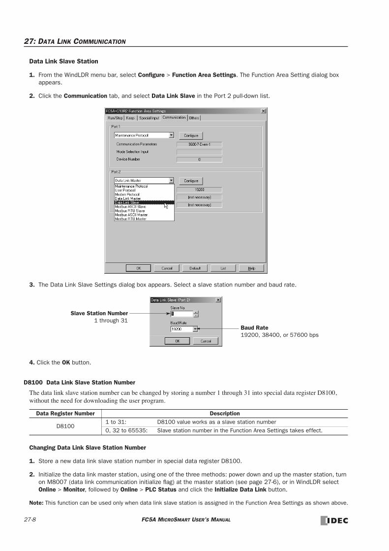
27: DATA LINK COMMUNICATION
Data Link Slave Station
1. From the WindLDR menu bar, select Configure > Function Area Settings. The Function Area Setting dialog box appears.
2. Click the Communication tab, and select Data Link Slave in the Port 2 pull-down list.
3. The Data Link Slave Settings dialog box appears. Select a slave station number and baud rate.
4. Click the OK button.
D8100 Data Link Slave Station Number
The data link slave station number can be changed by storing a number 1 through 31 into special data register D8100, without the need for downloading the user program.
Changing Data Link Slave Station Number
1. Store a new data link slave station number in special data register D8100.
2. Initialize the data link master station, using one of the three methods: power down and up the master station, turn on M8007 (data link communication initialize flag) at the master station (see page 27-6), or in WindLDR select Online > Monitor, followed by Online > PLC Status and click the Initialize Data Link button.
Note: This function can be used only when data link slave station is assigned in the Function Area Settings as shown above.
Data Register Number Description
D81001 to 31: D8100 value works as a slave station number0, 32 to 65535: Slave station number in the Function Area Settings takes effect.
Baud Rate 19200, 38400, or 57600 bps
Slave Station Number 1 through 31
27-8 FC5A MICROSMART USER’S MANUAL

27: DATA LINK COMMUNICATION
Data RefreshIn the data link communication, the master station communicates with only one slave station in one communication cycle. When a slave station receives a communication from the master station, the slave station returns data stored in data regis-ters assigned for data link communication. After receiving data from slave stations, the master station stores the data into data registers allocated to each slave station. The process of updating data into data registers is called refresh. When the maximum 31 slave stations are connected, the master station requires 31 communication cycles to communicate with all slave stations.
Note: When the data link system contains the MicroSmart (FC4A/FC5A) and MICRO3/MICRO3C, set the baud rate to 19200 bps and transmit/receive data quantity to 2 words in the Function Area Settings for the MicroSmart to communicate with MICRO3/MICRO3C stations.
Both master and slave stations refresh communication data at the END processing. When data refresh is complete, com-munication completion special internal relays M8080 through M8116 (slave station communication completion relay) go on at the master station for one scan time after the data refresh. At each slave station, special internal relay M8080 (com-munication completion relay) goes on.
When the master station completes communication with all slave stations, special internal relay M8117 (all slave station communication completion relay) goes on at the master station for one scan time.
Total Refresh Time at Master Station for Communication with All Slave Stations (Trfn)The master station requires the following time to refresh the transmit and receive data for communication with all slave stations, that is the total of refresh times.
[Baud Rate 19200 bps] Trfn = ∑ Trf = ∑ 4.2 ms + 2.4 ms × (Transmit Words + Receive Words) + 1 scan time[Baud Rate 38400 bps] Trfn = ∑ Trf = ∑ 2.2 ms + 1.3 ms × (Transmit Words + Receive Words) + 1 scan time[Baud Rate 57600 bps] Trfn = ∑ Trf = ∑ 1.6 ms + 0.9 ms × (Transmit Words + Receive Words) + 1 scan time
Example: Refresh TimeWhen data link communication is performed with such parameters as transmit words 6, receive words 6, slave stations 8, and average scan time 20 ms, then the total refresh time Trf8 for communication with all eight slave stations will be:
[Baud Rate 19200 bps] Trf8 = 4.2 ms + 2.4 ms × (6 + 6) + 20 ms × 8 = 424.0 ms[Baud Rate 38400 bps] Trf8 = 2.2 ms + 1.3 ms × (6 + 6) + 20 ms × 8 = 302.4 ms[Baud Rate 57600 bps] Trf8 = 1.6 ms + 0.9 ms × (6 + 6) + 20 ms × 8 = 259.2 ms
Mode Separate Refresh Mode
Scan TimeSince the communication between the master station and slave stations proceeds inde-pendently of the user program scanning, the scan time is not affected.
Data Refresh TimingAt both master and slave stations, received data is refreshed at the END processing. Refresh completion can be confirmed with communication completion special internal relays M8080 through M8117.
Applicable Master Station MicroSmart (FC4A/FC5A), OpenNet Controller, MICRO3, MICRO3C, FA-3S (PF3S-SIF4)
Applicable Slave Station MicroSmart (FC4A/FC5A), OpenNet Controller, MICRO3, MICRO3C, FA-3S (PF3S-SIF4)
FC5A MICROSMART USER’S MANUAL 27-9
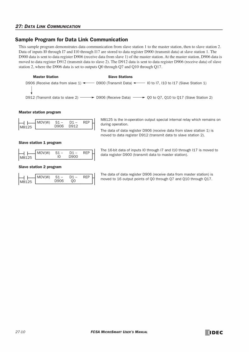
27: DATA LINK COMMUNICATION
Sample Program for Data Link CommunicationThis sample program demonstrates data communication from slave station 1 to the master station, then to slave station 2. Data of inputs I0 through I7 and I10 through I17 are stored to data register D900 (transmit data) at slave station 1. The D900 data is sent to data register D906 (receive data from slave 1) of the master station. At the master station, D906 data is moved to data register D912 (transmit data to slave 2). The D912 data is sent to data register D906 (receive data) of slave station 2, where the D906 data is set to outputs Q0 through Q7 and Q10 through Q17.
Master station program
Slave station 1 program
Slave station 2 program
Master Station Slave Stations
D906 (Receive data from slave 1)
D912 (Transmit data to slave 2)
D900 (Transmit Data)
D906 (Receive Data)
I0 to I7, I10 to I17 (Slave Station 1)
Q0 to Q7, Q10 to Q17 (Slave Station 2)
M8125 is the in-operation output special internal relay which remains on during operation.
The data of data register D906 (receive data from slave station 1) is moved to data register D912 (transmit data to slave station 2).
M8125REPS1 –
D906D1 –D912
MOV(W)
The 16-bit data of inputs I0 through I7 and I10 through I17 is moved to data register D900 (transmit data to master station).
M8125REPS1 –
I0D1 –D900
MOV(W)
The data of data register D906 (receive data from master station) is moved to 16 output points of Q0 through Q7 and Q10 through Q17.
M8125REPS1 –
D906D1 –Q0
MOV(W)
27-10 FC5A MICROSMART USER’S MANUAL

27: DATA LINK COMMUNICATION
Operating Procedure for Data Link SystemTo set up and use a data link system, complete the following steps:
1. Connect the MicroSmart CPU modules at the master station and all slave stations as illustrated on page 27-2.
2. Create user programs for the master and slave stations. Different programs are used for the master and slave sta-tions.
3. Using WindLDR, access Configure > Function Area Settings > Communication and make settings for the master and slave stations. For programming WindLDR, see pages 27-7 and 27-8.
4. Download the user programs to the master and slave stations.
5. To start data link communication, power up slave stations first, and power up the master station at least 1 second later. Monitor the data registers used for data link at the master and slave stations.
Note: To enable data link communication, power up slave stations first. If a slave station is powered up later than or at the same time with the master station, the master station does not recognize the slave station. To make the master station rec-ognize the slave station in this case, turn on special internal relay M8007 (data link communication initialize flag) at the master station (see page 27-6), or in WindLDR select Online > Monitor, followed by Online > PLC Status and click the Ini-tialize Data Link button.
Data Link Initialization ProgramIf the master station does not recognize the slave station when the master station is powered up, include the following pro-gram into the user program for the master station.
Initialize Data Link Initializes data link communication
M8120 M8007
M8120 is the initialize pulse special internal relay.
M8007 is the data link communication initialize flag.
When the master station CPU module starts to run, M8120 turns on M8007 for one scan to initialize the data link communication. The master station will recognize the slave station.
FC5A MICROSMART USER’S MANUAL 27-11

27: DATA LINK COMMUNICATION
Data Link with Other PLCsThe data link communication system can include IDEC’s OpenNet Controller, MICRO3/MICRO3C micro programmable controllers, and FA-3S programmable controllers using serial interface modules.
Data Link with OpenNet Controller
Data Link with FA-3S High-performance CPU using Serial Interface Module PF3S-SIF4
D8101 Data Link Transmit Wait Time (ms)
When a data link system consists of an FC5A master station and FA3S slave stations, store 20 to special data register D8101 of the FC5A CPU module at the master station. This way, the FC5A CPU module has a data link transmit wait time of 20 ms.
OpenNet Controller Settings MicroSmart Settings MicroSmart Settings
Transmit data: 6 wordsReceive data: 6 wordsBaud rate: 19200 or 38400 bps
Slave station number 1 Slave station number 2
FA-3S (PF3S-SIF4) Settings MicroSmart Settings MicroSmart Settings
Transmit data: 6 wordsReceive data: 6 wordsBaud rate: 19200 or 38400 bps
Slave station number 1 Slave station number 2
Data Register Number Description
D8101 20: D8101 value specifies data link transmit wait time in ms.
Slave Station 1
OpenNet Controller
Slave Station 2
Slave Station 1
FA-3S (CP12/13)PF3S-SIF4
Slave Station 2
27-12 FC5A MICROSMART USER’S MANUAL

28: COMPUTER LINK COMMUNICATION
IntroductionWhen the MicroSmart CPU module is connected to a computer, operating status and I/O status can be monitored on the computer, data in the CPU module can be monitored or updated, and user programs can be downloaded and uploaded. The CPU module can also be started and stopped from the computer. A maximum of 32 CPU modules can be connected to one computer in the 1:N computer link system.
The maximum communication speed in the 1:1 or 1:N computer link system is 57,600 bps.
This chapter describes the 1:N computer link system. For the 1:1 computer link system, see page 4-1.
Computer Link System Setup (1:N Computer Link System)To set up a 1:N communication computer link system, install the RS485 communication adapter (FC4A-PC3) to the port 2 connector on the all-in-one type CPU module, or mount the RS485 communication module (FC4A-HPC3) next to the slim type CPU module. Connect the RS232C/RS485 converter to the RS485 terminals A, B, and SG on every CPU module using a shielded twisted pair cable as shown below. The total length of the cable for the computer link system can be extended up to 200 meters (656 feet).
Connect the RS232C port on the computer to the RS232C/RS485 converter using the RS232C cable HD9Z-C52. The RS232C cable has a D-sub 9-pin female connector for connection with a computer.
FC4A MicroSmart, OpenNet Controllers, MICRO3, and MICRO3C can be connected to the same 1:N computer link system.
RS485CommunicationAdapterFC4A-PC3
RS485 Terminal on the Communication Module
A B SG
Cable
Port 1
Port 2
RS232C/RS485 ConverterFC2A-MD1
RS232C CableHD9Z-C521.5m (4.92 feet) long
1st Unit (Device No. 0)
2nd Unit (Device No. 1)
32nd Unit (Device No. 31)
A B SG
Cable
A B SG
Cable
Shielded twisted pair cable 200 meters (656 feet) maximum
Core wire 0.3 mm2
RS485 CommunicationModule FC4A-HPC3
FC5A MICROSMART USER’S MANUAL 28-1

28: COMPUTER LINK COMMUNICATION
Programming WindLDRIn the 1:1 computer link system, a computer can be connected to either port 1 or 2 on the MicroSmart CPU module. In the 1:N computer link system, a computer must be connected to port 2 on the CPU module and every CPU module must have a unique device number 0 through 31. The Communication page in the Function Area Settings must be programmed for each station in the computer link system. If required, communication parameters can also be changed.
Since these settings relate to the user program, the user program must be downloaded to the MicroSmart after changing any of these settings.
1. From the WindLDR menu bar, select Configure > Function Area Settings. The Function Area Setting dialog box appears.
2. Click the Communication tab, and select Maintenance Protocol in the Port 1 or 2 pull-down list.
3. Click the Configure button. The Communication Parameters dialog box appears. Change settings, if required.
4. Click the OK button.
Baud Rate (bps)1200, 2400, 4800, 9600, 19200,38400, 57600
Data Bits 7 or 8
Parity None, Odd, Even
Stop Bits 1 or 2
Receive Timeout (ms)10 to 2540 (10-ms increments) (Receive timeout is disabled when 2550 is selected.)
Device Number 0 to 31
Mode Selection Input Any input number
Note: When a mode selection input has been designated and the mode selection input is turned on, the selected communication parameters are enabled. When communication parameters are changed without designating a mode selection input, the changed communication parameters take effect immediately when the user program is down-loaded.
28-2 FC5A MICROSMART USER’S MANUAL
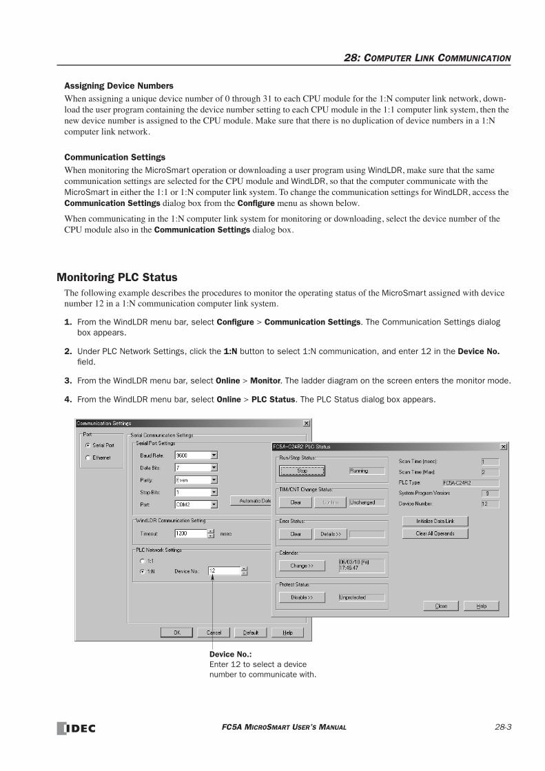
28: COMPUTER LINK COMMUNICATION
Assigning Device NumbersWhen assigning a unique device number of 0 through 31 to each CPU module for the 1:N computer link network, down-load the user program containing the device number setting to each CPU module in the 1:1 computer link system, then the new device number is assigned to the CPU module. Make sure that there is no duplication of device numbers in a 1:N computer link network.
Communication SettingsWhen monitoring the MicroSmart operation or downloading a user program using WindLDR, make sure that the same communication settings are selected for the CPU module and WindLDR, so that the computer communicate with the MicroSmart in either the 1:1 or 1:N computer link system. To change the communication settings for WindLDR, access the Communication Settings dialog box from the Configure menu as shown below.
When communicating in the 1:N computer link system for monitoring or downloading, select the device number of the CPU module also in the Communication Settings dialog box.
Monitoring PLC StatusThe following example describes the procedures to monitor the operating status of the MicroSmart assigned with device number 12 in a 1:N communication computer link system.
1. From the WindLDR menu bar, select Configure > Communication Settings. The Communication Settings dialog box appears.
2. Under PLC Network Settings, click the 1:N button to select 1:N communication, and enter 12 in the Device No. field.
3. From the WindLDR menu bar, select Online > Monitor. The ladder diagram on the screen enters the monitor mode.
4. From the WindLDR menu bar, select Online > PLC Status. The PLC Status dialog box appears.
Device No.: Enter 12 to select a device number to communicate with.
FC5A MICROSMART USER’S MANUAL 28-3

28: COMPUTER LINK COMMUNICATION
RS232C/RS485 Converter FC2A-MD1The RS232C/RS485 converter FC2A-MD1 is used to convert data signals between EIA RS232C and EIA RS485. This converter makes it possible to connect a host device with RS232C interface to multiple MicroSmart CPU modules using one cable.
Parts Description
Specifications
General Specifications
Serial Interface Specifications
Rated Power VoltagePower terminals:DC IN adapter jack:
24V DC ±20% (ripple 10% maximum)9V DC, 350mA supplied from AC adapter
Current Draw Power terminals: Approx. 40 mA at the rated voltageOperating Temperature 0 to 60°CStorage Temperature –20 to +70°COperating Humidity 45 to 85% RH (no condensation)Vibration Resistance 5 to 55 Hz, 60 m/sec2, 2 hours each in 3 axesShock Resistance 300 m/sec2, 3 shocks each in 3 axesDielectric Strength 1500V AC, 1 minute between live parts and dead partsInsulation Resistance 10 MΩ minimum between live parts and dead parts (500V DC megger)Noise Resistance Power terminals: ±1 kV, 1 µsec (using noise simulator)Weight Approx. 550g
Standards in ComplianceEIA standard RS232C (D-sub 25-pin female connector)EIA standard RS485 (screw terminals)
Communication Method Half-duplexCommunication Configuration 1:N (N ≤ 32)Communication Cable Shielded twisted-pair cableCommunication Baud Rate 9600 bps (fixed)Slave Stations 32 slave stations maximum (RS485 line)
Maximum Cable LengthRS232C: 15m (49.2 ft.) RS485: Total 200m (656 ft.)
RS232CSignal LevelConverter
RS485Signal Level
RS485 I/O
Termination ResistorTransmit/Receive Data ATransmit/Receive Data B
Signal Ground
Vcc (+24V)GND
Power IndicatorGoes on when power is supplied
Transmit Data IndicatorGoes on when RS232C transmit data (pin #2) is on
Receive Data IndicatorGoes on when RS232C receive data (pin #3) is on
RS232C I/OConnect to the RS232C port on the computer
AC Adapter Jack
Frame Ground
Note: Connect 24V DC to POWER SUPPLY + and – terminals or connect an AC adapter with 9V DC, 350mA output to the AC adapter jack.Note: The FC2A-MD1 contains a 220Ω termination resistor on the RS485 line, eliminating the need for an external termi-nation resistor. To use the internal termination resistor, connect terminal T to terminal B. When the termination resistor is not needed, disconnect terminal T from terminal B.
1
T2
A3
B4
SG5
FG6
+7
–
SD
RD
POWER
DC IN
RS485SERIAL PORT
POWER SUPPLY24V DC
RS
232C
SE
RIA
L P
OR
T
RS232C/RS485CONVERTER
Type FC2A-MD1
28-4 FC5A MICROSMART USER’S MANUAL

28: COMPUTER LINK COMMUNICATION
RS232C Connector Pinouts
Dimensions
RS232C Cable HD9Z-C52
AC AdapterThe RS232C/RS485 converter is powered by a 24V DC source or an AC adapter with 9V DC, 350mA output capacity.
Pin No. Description1 GND Frame Ground2 TXD Transmit Data3 RXD Receive Data4 (RTS) Unused5 (CTS) Unused6 (NC) Unused7 GND Signal Ground
8-25 (NC) Unused
113
1425
Note: Terminals 4 and 5 are connected together internally.
D-sub 25-pin Female Connector
110 mm (4.331")
10 mm (0.394")
132 mm (5.197")
3.6 mm
7 mm (0.276")
34 mm (1.339")
AC Adapter Jack
Mounting Bracket
5 mm
Rubber Feet
24.4 mm
3.6 mm
D-sub 25-pin Connector
ø4.5 mm hole × 2
142 mm
10 mm (0.394")
(0.142")3.6 mm(0.142")
(0.142")
3.6 mm(0.142")
(0.197")
(0.961")
(5.591")
(0.177" dia.)
Note: When mounting the RS232C/RS485 converter on a panel surface, remove the rubber feet; then attach the supplied mounting brackets on the bottom of the converter using screws.
Mounting Hole Layout
Connector for RS232C/RS485 Converter
D-sub 25-pin male connector
Description Pin No.GND Frame Ground 1TXD Transmit Data 2RXD Receive Data 3RTS Request to Send 4CTS Clear to Send 5DSR Data Set Ready 6DCD Data Carrier Detect 8DTR Data Terminal Ready 20GND Signal Ground 7
Connector for Computer
D-sub 9-pin female connector
Pin No. Symbol1 DCD2 RXD3 TXD4 DTR5 GND6 DSR7 RTS8 CTS9 RI
1.5m (4.92 ft.) long
9.5ø2.1ø5
.5 Polarity
+ –
Dimensions in mm.
FC5A MICROSMART USER’S MANUAL 28-5

28: COMPUTER LINK COMMUNICATION
28-6 FC5A MICROSMART USER’S MANUAL
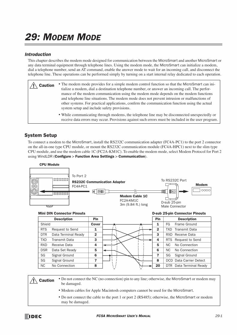
29: MODEM MODE
Introduction This chapter describes the modem mode designed for communication between the MicroSmart and another MicroSmart or any data terminal equipment through telephone lines. Using the modem mode, the MicroSmart can initialize a modem, dial a telephone number, send an AT command, enable the answer mode to wait for an incoming call, and disconnect the telephone line. These operations can be performed simply by turning on a start internal relay dedicated to each operation.
System SetupTo connect a modem to the MicroSmart, install the RS232C communication adapter (FC4A-PC1) to the port 2 connector on the all-in-one type CPU module, or mount the RS232C communication module (FC4A-HPC1) next to the slim type CPU module, and use the modem cable 1C (FC2A-KM1C). To enable the modem mode, select Modem Protocol for Port 2 using WindLDR (Configure > Function Area Settings > Communication).
Caution • The modem mode provides for a simple modem control function so that the MicroSmart can ini-tialize a modem, dial a destination telephone number, or answer an incoming call. The perfor-mance of the modem communication using the modem mode depends on the modem functions and telephone line situations. The modem mode does not prevent intrusion or malfunctions of other systems. For practical applications, confirm the communication function using the actual system setup and include safety provisions.
• While communicating through modems, the telephone line may be disconnected unexpectedly or receive data errors may occur. Provisions against such errors must be included in the user program.
Modem Cable 1CFC2A-KM1C 3m (9.84 ft.) long
To RS232C Port
D-sub 25-pin Male Connector
D-sub 25-pin Connector Pinouts
Pin Description1 FG Frame Ground2 TXD Transmit Data3 RXD Receive Data4 RTS Request to Send5 NC No Connection6 NC No Connection7 SG Signal Ground8 DCD Data Carrier Detect20 DTR Data Terminal Ready
Modem
Mini DIN Connector Pinouts
Description PinShield CoverRTS Request to Send 1DTR Data Terminal Ready 2TXD Transmit Data 3RXD Receive Data 4DSR Data Set Ready 5SG Signal Ground 6SG Signal Ground 7NC No Connection 8
Caution • Do not connect the NC (no connection) pin to any line; otherwise, the MicroSmart or modem may be damaged.
• Modem cables for Apple Macintosh computers cannot be used for the MicroSmart.
• Do not connect the cable to the port 1 or port 2 (RS485); otherwise, the MicroSmart or modem may be damaged.
To Port 2
RS232C Communication AdapterFC4A-PC1
CPU Module
FC5A MICROSMART USER’S MANUAL 29-1
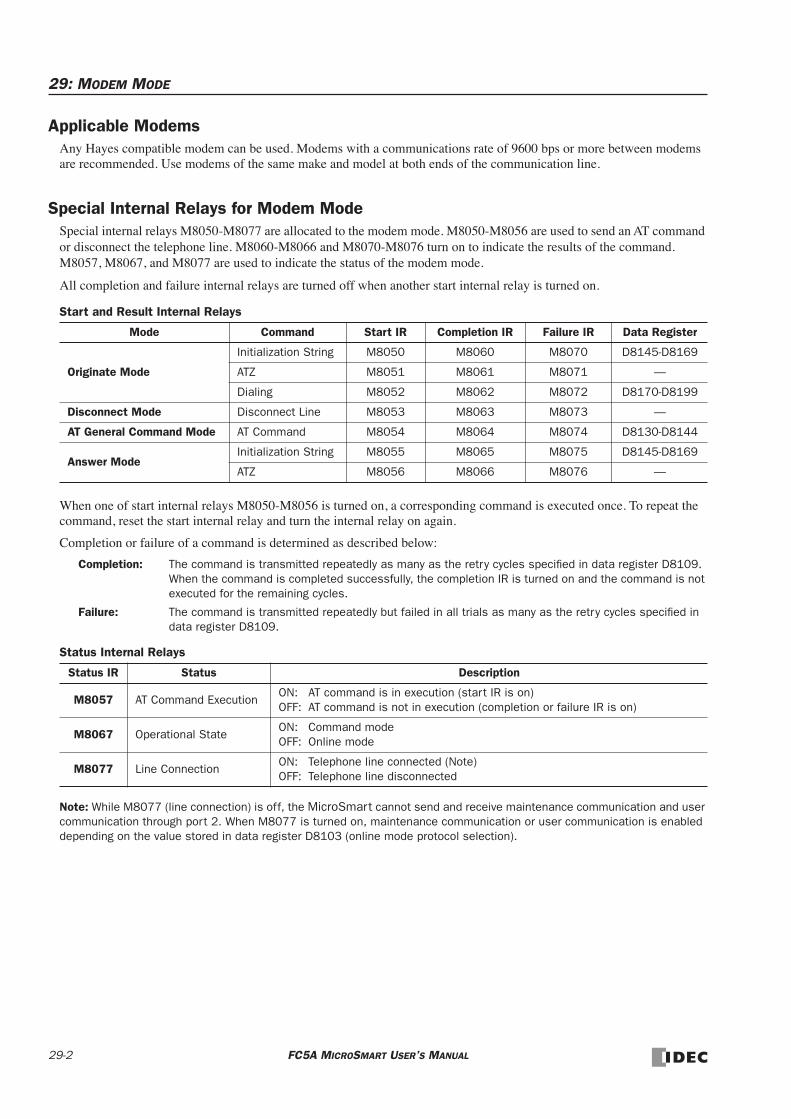
29: MODEM MODE
Applicable ModemsAny Hayes compatible modem can be used. Modems with a communications rate of 9600 bps or more between modems are recommended. Use modems of the same make and model at both ends of the communication line.
Special Internal Relays for Modem ModeSpecial internal relays M8050-M8077 are allocated to the modem mode. M8050-M8056 are used to send an AT command or disconnect the telephone line. M8060-M8066 and M8070-M8076 turn on to indicate the results of the command. M8057, M8067, and M8077 are used to indicate the status of the modem mode.
All completion and failure internal relays are turned off when another start internal relay is turned on.
Start and Result Internal Relays
When one of start internal relays M8050-M8056 is turned on, a corresponding command is executed once. To repeat the command, reset the start internal relay and turn the internal relay on again.
Completion or failure of a command is determined as described below:
Completion: The command is transmitted repeatedly as many as the retry cycles specified in data register D8109. When the command is completed successfully, the completion IR is turned on and the command is not executed for the remaining cycles.
Failure: The command is transmitted repeatedly but failed in all trials as many as the retry cycles specified in data register D8109.
Status Internal Relays
Note: While M8077 (line connection) is off, the MicroSmart cannot send and receive maintenance communication and user communication through port 2. When M8077 is turned on, maintenance communication or user communication is enabled depending on the value stored in data register D8103 (online mode protocol selection).
Mode Command Start IR Completion IR Failure IR Data Register
Originate Mode
Initialization String M8050 M8060 M8070 D8145-D8169
ATZ M8051 M8061 M8071 —
Dialing M8052 M8062 M8072 D8170-D8199
Disconnect Mode Disconnect Line M8053 M8063 M8073 —
AT General Command Mode AT Command M8054 M8064 M8074 D8130-D8144
Answer ModeInitialization String M8055 M8065 M8075 D8145-D8169
ATZ M8056 M8066 M8076 —
Status IR Status Description
M8057 AT Command ExecutionON: AT command is in execution (start IR is on)OFF: AT command is not in execution (completion or failure IR is on)
M8067 Operational StateON: Command modeOFF: Online mode
M8077 Line ConnectionON: Telephone line connected (Note)OFF: Telephone line disconnected
29-2 FC5A MICROSMART USER’S MANUAL

29: MODEM MODE
Special Data Registers for Modem ModeSpecial data registers D8103 and D8109-D8199 are allocated to the modem mode. When the MicroSmart starts to run, D8109 and D8110 store the default values, and D8145-D8169 store the default initialization string.
Originate ModeThe originate mode is used to send an initialization string to the modem, issue the ATZ command to reset the modem, and dial the telephone number. To execute a command, turn on one of start internal relays M8050-M8052. If two or more start internal relays are turned on simultaneously, an error will result and error code 61 is stored in modem mode status data register D8111 (see page 29-7). When a start internal relay is turned on, a corresponding sequence of commands is exe-cuted once as described below. When the start command fails, the same command is repeated as many as the retry cycles specified by D8109.
M8050: Send an initialization string, send the ATZ command, and dial the telephone number
M8051: Send the ATZ command and dial the telephone number
M8052: Dial the telephone number
Initialization String in Originate ModeWhen the modem mode is enabled as described on page 29-1 and the MicroSmart is started to run, the default initialization string is stored to data registers D8145-D8169 at the END processing of the first scan. To send the initialization string from the MicroSmart to the modem, turn M8050 on; then the ATZ command is issued and the telephone number is dialed suc-cessively.
Default Initialization String: ATE0Q0V1&D2&C1\V0X4&K3\A0\N5S0=2&W
Data Register Stored Data Description
D8103Online Mode Protocol Selection
The D8103 value selects the protocol for the RS232C port 2 after telephone line is connected.
0 (other than 1): Maintenance protocol1: User protocol
D8109Retry Cycles(default = 3)
The D8109 value selects how many retries will be made until the operation initi-ated by a start internal relay M8050-M8056 is completed.
0: No retry1-65535: Executes a specified number of retries
D8110Retry Interval(default = 90 sec)
The D8110 value specifies the interval to start a retry of dialing when a dialing fails with the retry cycles set to a value more than 1. (Other start commands are repeated continuously as many as the retry cycles.)
Valid value: 0 to 65535 (seconds)
If a telephone line is not connected within the retry interval, the MicroSmart starts a retry. Consequently, if the retry interval is set to a too small value, the telephone line can not be connected correctly.
D8111Modem Mode Status
Modem mode status is stored (see page 29-7). When not in the modem mode, D8111 stores 0.
D8115-D8129AT Command Result Code
AT command result codes returned from modem are stored. When the result code exceeds 30 bytes, first 30 bytes are stored.
D8130-D8144AT Command String
AT command string for the AT general command mode is stored. Enter an AT command string to these data registers to send by turning on M8054 (AT com-mand start internal relay). “AT” and LF (0Ah) are appended automatically.
D8145-D8169 Initialization String
Initialization string for the originate and answer modes is stored.
To change the initialization string, enter a new value to these data registers. The new value is sent by turning on M8050 or M8055. “AT” and LF (0Ah) are appended automatically.
D8170-D8199 Telephone NumberTelephone number for dialing in the originate mode is stored. “ATD” and LF (0Ah) are appended automatically.
CR LF
FC5A MICROSMART USER’S MANUAL 29-3

29: MODEM MODE
AT and are appended at the beginning and end of the initialization string automatically by the system program and are not stored in data registers.
Depending on your modem and telephone line, the initialization string may have to be modified. Consult the manual for your modem.
Changes can be made by entering required values to data registers D8145-D8169. Store two characters in one data regis-ter; the first character at the upper byte and the second character at the lower byte in the data register. AT and need not be stored in data registers. Use the MOV (move) instructions on WindLDR to set the initialization string characters and ASCII value 0Dh for at the end. Program the MOV instructions to replace the default values in D8145-D8169 stored in the first scan and execute the MOV instructions in a subsequent scan. For essential commands which must be included in the initialization string, see page 29-8. After the new values are stored, turn on M8050 to send the new initialization string to the modem.
When the initialization string has been sent successfully, internal relay M8060 is turned on. If the initialization string fails, internal relay M8070 is turned on. When the subsequent commands of ATZ and dialing are also completed successfully, M8061 and M8062 will also be turned on.
The default initialization string or the modified initialization string stored in D8145-D8169 is also used for the initializa-tion in the answer mode.
ATZ (Resetting the Modem) in Originate ModeThe default initialization string specifies to be stored in the non-volatile memory of the modem, using the &W command. The initialization string is restored when the modem is powered up or when the ATZ command is issued. The MicroSmart sends the ATZ command to the modem, following the initialization string when M8050 is turned on. The ATZ command can also be issued separately by turning M8051 on, followed by the dial command to be executed automatically.
ATZ Command: ATZ
When the ATZ command has been completed successfully, internal relay M8061 is turned on. If the ATZ command fails, internal relay M8071 is turned on. When the subsequent dialing is also completed successfully, M8062 will also be turned on.
If the initialization string has been stored in the non-volatile memory of the modem, M8050 may be skipped. Start with M8051 to send the ATZ command.
Dialing the Telephone NumberData registers D8170-D8199 are allocated to the telephone number. Before turning on one of the start internal relays M8050-M8052 for the originate mode, store the telephone number in data registers starting with D8170. One data register stores two characters: the first character at the upper byte and the second character at the lower byte in the data register. Since 30 data registers are allocated to the telephone number, up to 60 characters can be stored, as many as the modem capacity allows. Use the MOV (move) instructions on WindLDR to set the telephone number and execute the MOV instruc-tions before turning on start internal relays M8050-M8052.
Example of Dial Command: ATD1234
ATD and are appended at the beginning and end of the dial command automatically by the system program and need not be stored in data registers. To program the telephone number of the example above, store the telephone number and ASCII value 0Dh for to data registers starting with D8170. It is also possible to store character T for touch-tone phone or P for pulse or rotary phone.
LF
0D008161
Q08146
V18147
&D8148
2&8149
C18150
\V8151
0X8152
4&8153
K38154
\A8155
0\8156
N58157
S08158
=28159
&W8160
E08145
ATDR
LF
LF
CR
CR LF
CR LF
LF
CR
3132hD8170
3334hD8171
0D00hD8172
31h = “1” 32h = “2”33h = “3” 34h = “4”
0Dh = All characters subsequent to CR are ignored.CR
29-4 FC5A MICROSMART USER’S MANUAL

29: MODEM MODE
As described above, when start internal relay M8050 is turned on, the initialization string is sent, followed by the ATZ command and the dial command. When start internal relay M8051 is turned on, the ATZ command is sent, followed by the dial command. The dial command can also be sent separately by turning on start internal relay M8052.
If retry cycles are set to data register D8109, the dial command is repeated at retry intervals specified by D8110 (default 90 seconds) as many as the specified retry cycles (default 3 cycles) until the telephone line is connected.
When the dial command has been completed successfully, internal relay M8062 is turned on. If the dial command fails, internal relay M8072 is turned on.
The dial command is determined successful when the DCD signal is turned on.
Note: When the MicroSmart is powered down while the telephone line is connected, the telephone line is disconnected because the DTR signal is turned off. This method should not be used for disconnecting the telephone line. Always use M8053 to disconnect the telephone line as described below.
RS232C Port Communication ProtocolBefore the telephone line is connected in the modem mode after powerup, the RS232C port 2 can only send out an AT command by turning on a start internal relay M8050-M8056. The communication protocol for the RS232C port 2 after the telephone line is connected is selected by the value stored in data register D8103.
When the telephone line is disconnected, the RS232C port 2 restores the state as before the telephone line was connected, whether D8103 is set to 0 or 1.
When using a TXD or RXD instruction in the user communication mode while the telephone line is connected, insert internal relay M8077 (line connection) as an input condition for the TXD or RXD instruction. After the telephone line is connected, make sure of an approximately 1-second interval before executing the TXD or RXD instruction until the tele-phone line connection stabilizes.
Note: When the MicroSmart is stopped while the telephone line is connected, the RS232C port 2 protocol changes to the maintenance protocol even if D8103 is set to 1 (user protocol in the online mode); then the telephone line remains con-nected. When the MicroSmart is restarted, the user protocol is enabled again.
Disconnect ModeThe disconnect mode includes only one command to disconnect the telephone line. To disconnect the telephone line, turn on internal relay M8053. The telephone line is disconnected by turning off the DTR signal since the initialization string includes the &D2 command.
While a modem command is executed, another command cannot be executed. If two or more start internal relays are turned on simultaneously, an error will result and error code 61 is stored in modem mode status data register D8111 (see page 29-7).
When the disconnect command has been completed successfully, internal relay M8063 is turned on. If the disconnect com-mand fails, internal relay M8073 is turned on.
The disconnect command is determined successful when the DCD signal is turned off.
After the telephone line is disconnected, the RS232C port 2 restores the state as before the telephone line was connected whether D8103 is set to 0 or 1 so that the RS232C port 2 can be controlled by turning on a start internal relay M8050-M8056.
AT General Command ModeData registers D8130-D8144 are allocated to the AT command string. Before turning on start internal relay M8054 for the AT general command mode, store an AT command string in data registers starting with D8130. One data register stores two characters: the first character at the upper byte and the second character at the lower byte in the data register. Use the MOV (move) instructions on WindLDR to set the AT command string and execute the MOV instructions before turning M8054 on.
D8103 Value RS232C Port 2 Communication Protocol in the Online Mode
0 (other than 1) Maintenance protocol
1 User protocol
FC5A MICROSMART USER’S MANUAL 29-5

29: MODEM MODE
Example of AT Command: ATE0Q0V1
AT and are appended at the beginning and end of the AT general command string automatically by the system program and need not be stored in data registers. To program the AT command string of the example above, store the command characters and ASCII value 0Dh for to data registers starting with D8130.
When the AT general command has been completed successfully, internal relay M8064 is turned on. If the AT general command fails, internal relay M8074 is turned on.
The AT general command is determined successful when result code OK returned from the modem is received.
Answer ModeThe answer mode is used to send an initialization string to the modem and to issue the ATZ command to reset the modem. To execute a command, turn on one of start internal relays M8055 or M8056. If two or more start internal relays are turned on simultaneously, an error will result and error code 61 is stored in modem mode status data register D8111 (see page 29-7). When a start internal relay is turned on, a corresponding sequence of commands is executed once as described below.
M8055: Send initialization string and send the ATZ command
M8056: Send the ATZ command
Initialization String in Answer ModeWhen the modem mode is enabled as described on page 29-1 and the MicroSmart is started to run, the default initialization string is stored to data registers D8145-D8169 at the END processing of the first scan. To send the initialization string from the data registers to the modem, turn M8055 on; then the ATZ command is issued subsequently.
Default Initialization String: ATE0Q0V1&D2&C1\V0X4&K3\A0\N5S0=2&W
As described in the Originate Mode, the initialization string can be modified to match your modem. For details of modify-ing the initialization string, see page 29-3.
When the initialization string has been sent successfully, internal relay M8065 is turned on. If the initialization string fails, internal relay M8075 is turned on. When the subsequent ATZ command is also completed successfully, M8066 will also be turned on.
ATZ (Resetting the Modem) in Answer ModeThe default initialization string specifies to be stored in the non-volatile memory of the modem, using the &W command. The initialization string is restored when the modem is powered up or when the ATZ command is issued. The MicroSmart sends the ATZ command to the modem following the initialization string when M8055 is turned on. The ATZ command can also be issued separately by turning M8056 on.
ATZ Command: ATZ
When the ATZ command has been completed successfully, internal relay M8066 is turned on. If the ATZ command fails, internal relay M8076 is turned on.
If the initialization string has been stored in the non-volatile memory of the modem, M8055 may be skipped. Start with M8056 to send the ATZ command.
CR LF
LF
CR
4530hD8130
5130hD8131
5631hD8132
45h = “E” 30h = “0”51h = “Q” 30h = “0”
56h = “V” 31h = “1”
0D00hD8133 0Dh = All characters subsequent to CR are ignored.CR
CR LF CR LF
CR LF
CR LF
29-6 FC5A MICROSMART USER’S MANUAL
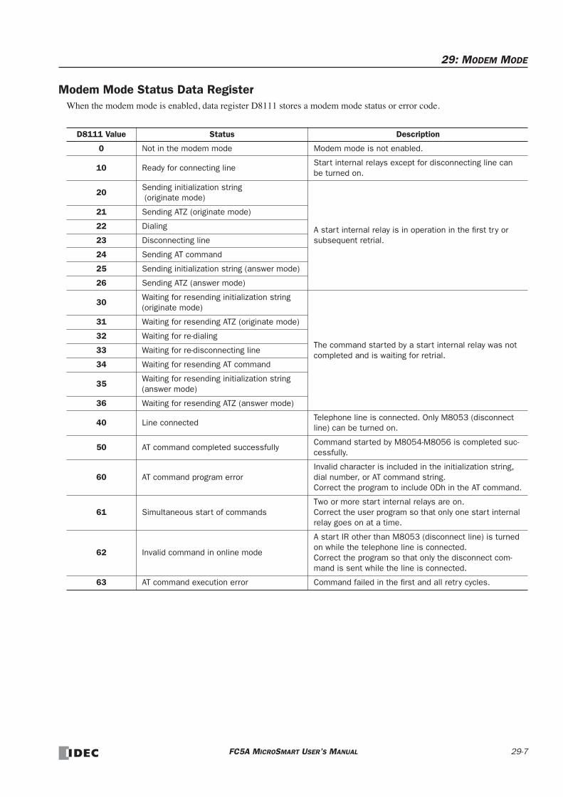
29: MODEM MODE
Modem Mode Status Data RegisterWhen the modem mode is enabled, data register D8111 stores a modem mode status or error code.
D8111 Value Status Description
0 Not in the modem mode Modem mode is not enabled.
10 Ready for connecting lineStart internal relays except for disconnecting line can be turned on.
20Sending initialization string (originate mode)
A start internal relay is in operation in the first try or subsequent retrial.
21 Sending ATZ (originate mode)
22 Dialing
23 Disconnecting line
24 Sending AT command
25 Sending initialization string (answer mode)
26 Sending ATZ (answer mode)
30Waiting for resending initialization string (originate mode)
The command started by a start internal relay was not completed and is waiting for retrial.
31 Waiting for resending ATZ (originate mode)
32 Waiting for re-dialing
33 Waiting for re-disconnecting line
34 Waiting for resending AT command
35Waiting for resending initialization string (answer mode)
36 Waiting for resending ATZ (answer mode)
40 Line connectedTelephone line is connected. Only M8053 (disconnect line) can be turned on.
50 AT command completed successfullyCommand started by M8054-M8056 is completed suc-cessfully.
60 AT command program errorInvalid character is included in the initialization string, dial number, or AT command string. Correct the program to include 0Dh in the AT command.
61 Simultaneous start of commandsTwo or more start internal relays are on. Correct the user program so that only one start internal relay goes on at a time.
62 Invalid command in online mode
A start IR other than M8053 (disconnect line) is turned on while the telephone line is connected. Correct the program so that only the disconnect com-mand is sent while the line is connected.
63 AT command execution error Command failed in the first and all retry cycles.
FC5A MICROSMART USER’S MANUAL 29-7

29: MODEM MODE
Initialization String CommandsThe built-in initialization string (see page 29-3) include the commands shown below. For details of modem commands, see the user’s manual for your modem. When you make an optional initialization string, modify the initialization string to match your modem.
E0
Characters NOT echoed.The modem mode of the MicroSmart operates without echo back. Without the E0 command, the MicroSmart misunderstands an echo for a result code. An error will be caused although a command is executed correctly.This command must be included in the initialization string.
Q0
Result codes displayed.The modem mode of the MicroSmart is configured to use result codes. Without the Q0 command, a timeout error will be caused although a command is executed correctly.This command must be included in the initialization string.
V1
Word result code.The modem mode of the MicroSmart is configured to use word result codes. Without the V1 com-mand, result codes are regarded as invalid and a timeout error will be caused although a command is executed correctly.This command must be included in the initialization string.
&D2
Hang up and disable auto-answer on DTR detection.When the DTR signal turns off, the telephone line is disconnected. The MicroSmart uses this function to disconnect the telephone line.This command must be included in the initialization string.
&C1
DCD ON with carrier from remote modem.DCD tracks the state of the data carrier from the remote modem. An ON condition of DCD indicates the presence of a carrier.This command must be included in the initialization string.
\V0MNP result codes disabled.Conventional result codes are used and reliable link result codes are not used.
X4 Enables dial tone and busy detection.
&K3Enables hardware flow control. The software flow control (XON/XOFF) cannot be used for the MicroSmart modem mode.This command must be included in the initialization string.
\A0 Set MNP maximum block size to 64 bytes.
\N5 MNP auto-reliable mode
S0=2Ring to answer ON.Specifies the ring on which the modem will pick up the telephone line. S0=2 specifies that the modem answers an incoming call when detecting 2 ring calls. S0=0 disables the auto-answer function.
&WWrite active profile.The current configuration profile is saved to a non-volatile memory of the modem.
29-8 FC5A MICROSMART USER’S MANUAL

29: MODEM MODE
Preparations for Using ModemBefore using a modem, read the user’s manual for your modem.
The required initialization string depends on the model and make of the modem. When the MicroSmart starts to run the user program, the default modem initialization strings is stored to D8145-D8169. See page 29-3.
Default Initialization String: ATE0Q0V1&D2&C1\V0X4&K3\A0\N5S0=2&W
Programming Data Registers and Internal RelaysTo enable the modem mode and communicate through the telephone line, the following settings are needed.
1. If the default initialization string does not match your modem, program a proper initialization string and enter the ASCII values to data registers starting with D8145 (initialization string). To send out the new initialization string, turn on internal relay M8050 (initialization string start IR) after the new values have been stored to the data regis-ters.
2. Program to move 0 or 1 to data register D8103 (online mode protocol selection) to select maintenance protocol or user protocol for the RS232C port 2 after telephone line is connected.
3. Program the destination telephone number if dialing is required. Enter the ASCII values of the telephone number to data registers starting with D8170 (telephone number). Store two characters each in one data register. Enter 0Dh at the end of the telephone number. See page 29-4.
4. If you want to change the default value of 3 retry cycles, program to move a required value to data register D8109.
5. Include internal relays M8050-M8077 in the user program to control the modem communication as required.
Setting Up the CPU Module
1. Install the RS232C communication adapter (FC4A-PC1) to the port 2 connector on the all-in-one type CPU module.
When using any slim type CPU module, mount the RS232C communication module (FC4A-HPC1) next to the slim type CPU module, and use the port 2 on the RS232C communication module.
When using the HMI base module with any slim type CPU module, install the RS232C communication adapter (FC4A-PC1) to the port 2 connector on the HMI base module.
2. Connect the MicroSmart CPU module port 2 to a modem using the modem cable 1C (FC2A-KM1C) as shown on page 29-1.
CR LF
FC5A MICROSMART USER’S MANUAL 29-9

29: MODEM MODE
Programming WindLDRThe Communication page in the Function Area Settings must be programmed to enable the modem communication for port 2. If required, communication parameters of the CPU module port 2 can also be changed.
Since these settings relate to the user program, the user program must be downloaded to the MicroSmart after changing any of these settings.
1. From the WindLDR menu bar, select Configure > Function Area Settings. The Function Area Setting dialog box appears.
2. Click the Communication tab, and select Modem Protocol in the Port 2 pull-down list.
3. Click the Configure button. The Communication Parameters dialog box appears. Change settings, if required.
The default communication parameters shown below are recommended.
4. Click the OK button.
Baud rate 9600 bps Only when the modem connected on the communication line uses differ-ent communication parameters than the default values of the MicroSmart, set the matching communication parameters. Since the total of modem communication parameters is 10 bits, set the value to a total of 10 bits.
Start bit 1Data bits 7Parity EvenStop bit 1Total 10 bits
Baud Rate (bps)1200, 2400, 4800, 9600, 19200,38400, 57600
Data Bits 7 or 8
Parity None, Odd, Even
Stop Bits 1 or 2
Receive Timeout (ms)10 to 2540 (10-ms increments) (Receive timeout is disabled when 2550 is selected.)
Device Number 0 to 31
29-10 FC5A MICROSMART USER’S MANUAL

29: MODEM MODE
Operating Procedure for Modem Mode
1. After completing the user program including the Function Area Settings, download the user program to the Micro-Smart from a computer running WindLDR.
2. Start the MicroSmart to run the user program.
3. Turn on start internal relay M8050 or M8055 to initialize the modem.
When originating the modem communication, turn on M8050 to send the initialization string, the ATZ command, and the dial command. If the initialization string has been stored in the non-volatile memory of the modem, turn on M8051 to start with the ATZ command followed by the dial command.
When answering an incoming call, turn on M8055 to send the initialization string and the ATZ command. If the ini-tialization string has been stored in the non-volatile memory of the modem, turn on M8056 to send the ATZ com-mand only.
4. Transmit or receive communication through the modem.
5. Turn on start internal relay M8053 to disconnect the telephone line.
FC5A MICROSMART USER’S MANUAL 29-11
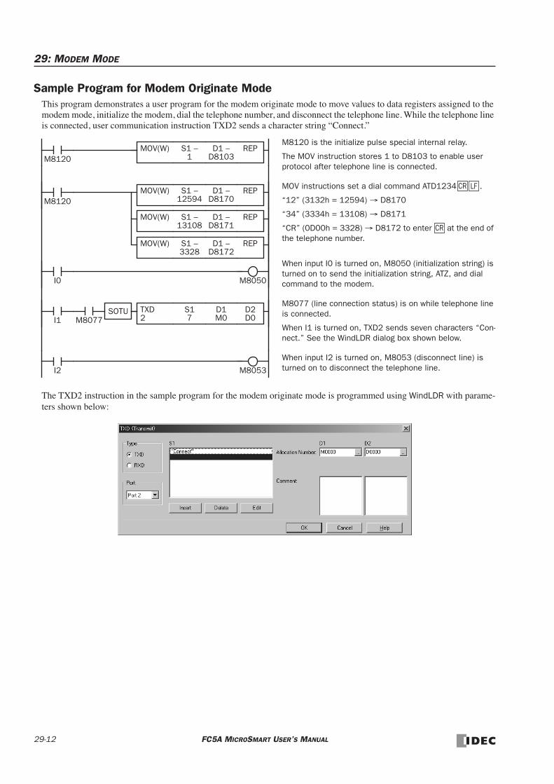
29: MODEM MODE
Sample Program for Modem Originate ModeThis program demonstrates a user program for the modem originate mode to move values to data registers assigned to the modem mode, initialize the modem, dial the telephone number, and disconnect the telephone line. While the telephone line is connected, user communication instruction TXD2 sends a character string “Connect.”
The TXD2 instruction in the sample program for the modem originate mode is programmed using WindLDR with parame-ters shown below:
M8120 is the initialize pulse special internal relay.
The MOV instruction stores 1 to D8103 to enable user protocol after telephone line is connected.
MOV instructions set a dial command ATD1234 .
“12” (3132h = 12594) → D8170
“34” (3334h = 13108) → D8171
“CR” (0D00h = 3328) → D8172 to enter at the end of the telephone number.
When input I0 is turned on, M8050 (initialization string) is turned on to send the initialization string, ATZ, and dial command to the modem.
M8077 (line connection status) is on while telephone line is connected.
When I1 is turned on, TXD2 sends seven characters “Con-nect.” See the WindLDR dialog box shown below.
When input I2 is turned on, M8053 (disconnect line) is turned on to disconnect the telephone line.
CR LF
CR
M8120REPS1 –
1D1 –
D8103MOV(W)
I0
I1 M8077SOTU D2
D0S17
D1M0
TXD2
I2
M8050
M8053
M8120REPS1 –
12594D1 –
D8170MOV(W)
REPS1 –13108
D1 –D8171
MOV(W)
REPS1 –3328
D1 –D8172
MOV(W)
29-12 FC5A MICROSMART USER’S MANUAL

29: MODEM MODE
Sample Program for Modem Answer ModeThis program demonstrates a user program for the modem answer mode to move a value to a data register assigned to the modem mode and initialize the modem. While the telephone line is connected, user communication instruction RXD2 is executed to receive an incoming communication.
The RXD2 instruction is programmed using WindLDR with parameters shown below:
Source S1: Data register D10, No conversion, 2 digits, Repeat 10
M8120 is the initialize pulse special internal relay.
When the MicroSmart starts to run, M8055 is turned on to send the initialization string for the modem answer mode.
The MOV instruction stores 1 to D8103 to enable user protocol after telephone line is connected.
M8077 (line connection status) is on while telephone line is con-nected.
RXD2 receives incoming communication and stores received data to data registers starting with D10.
M8120
M8120REPS1 –
1D1 –
D8103MOV(W)
M8077D2D0
S120
D1M0
RXD2
M8055
FC5A MICROSMART USER’S MANUAL 29-13

29: MODEM MODE
Troubleshooting in Modem Communication
When a start internal relay is turned on, the data of D8111 (modem mode status) changes, but the modem does not work.
Cause: A wrong cable is used or wiring is incorrect.
Solution: Use the modem cable 1C (FC2A-KM1C).
The DTR or ER indicator on the modem does not turn on.
Cause: A wrong cable is used or wiring is incorrect.
Solution: Use the modem cable 1C (FC2A-KM1C).
When a start internal relay is turned on, the data of D8111 (modem mode status) does not change.
Cause: Modem protocol is not selected for port 2.
Solution: Select Modem Protocol for Port 2 using WindLDR (Configure > Function Area Settings > Communica-tion) and download the user program to the CPU module.
When an initialization string is sent, a failure occurs, but sending ATZ completes successfully.
Cause: The initialization string is not valid for the modem.
Solution: Refer to the user’s manual for the modem and correct the initialization string.
When a dial command is sent, a result code “NO DIALTONE” is returned and the telephone line is not connected.
Cause 1: The modular cable is not connected.
Solution 1: Connect the modular cable to the modem.
Cause 2: The modem is used in a PBX environment.
Solution 2: Add X0 or X3 to the initialization string stored in data registers D8145-D8169, and try initialization again.
Dialing completes successfully, but the telephone line is disconnected in a short period of time.
Cause 1: The modem settings at the both ends of the line are different.
Solution 1: Make the same settings for the modems at the both ends.
Cause 2: The model of the modems at the both ends of the line is different.
Solution 2: Use the same modems at the both ends.
Cause 3: The quality of the telephone line is low.
Solution 3: Decrease the baud rate of the MicroSmart to lower than 9600 bps.
29-14 FC5A MICROSMART USER’S MANUAL

30: MODBUS COMMUNICATION
IntroductionThis chapter describes the Modbus master and slave communication function of the MicroSmart CPU module.
All FC5A MicroSmart CPU modules can be connected to the Modbus network using communication port 2 through the RS485 or RS232C line. The MicroSmart Modbus communication function is compatible with ASCII and RTU modes.
Modbus Communication System SetupTo set up a 1:N Modbus communication system, install the RS485 communication adapter (FC4A-PC3) to the port 2 con-nector on the all-in-one type CPU module.
When using the slim type CPU module, mount the RS485 communication module (FC4A-HPC3) next to the CPU module.
When using the optional HMI module with the slim type CPU module, install the RS485 communication adapter (FC4A-PC3) to the port 2 connector on the HMI base module.
Connect the RS485 terminals A, B, and SG on every CPU module using a shielded twisted pair cable as shown below. The total length of the cable for the RS485 Modbus communication system can be extended up to 200 meters (656 feet).
To set up RS232C communication system, use RS232C communication adapter (FC4A-PC1) or RS232C communication module (FC4A-HPC1). The RS232C can set up only 1:1 communication system.
A B SG
Cable Cable
A B SG
Master Station Slave Station 1
Slave Station 2Slave Station 31
RS485 Communication Adapter FC4A-PC3
on Port 2 Connector
RS485 Communication Module FC4A-HPC3
All-in-One Type CPU Module
Slim Type CPU Module
Shielded twisted pair cable 200 meters (656 feet) maximum
Core wire 0.3mm2
Mini DIN connector type RS485 communication adapter FC4A-PC2 or RS485 communication module FC4A-HPC2 can also be used.
RS485 Communication Adapter FC4A-PC3
on Port 2 Connector
HMI Base Module FC4A-HPH1
FC5A MICROSMART USER’S MANUAL 30-1
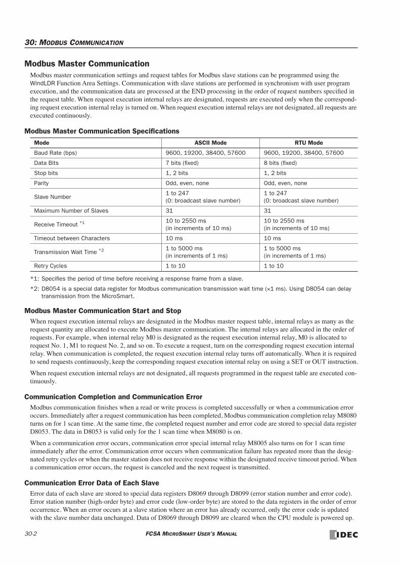
30: MODBUS COMMUNICATION
Modbus Master CommunicationModbus master communication settings and request tables for Modbus slave stations can be programmed using the WindLDR Function Area Settings. Communication with slave stations are performed in synchronism with user program execution, and the communication data are processed at the END processing in the order of request numbers specified in the request table. When request execution internal relays are designated, requests are executed only when the correspond-ing request execution internal relay is turned on. When request execution internal relays are not designated, all requests are executed continuously.
Modbus Master Communication Specifications
*1: Specifies the period of time before receiving a response frame from a slave.
*2: D8054 is a special data register for Modbus communication transmission wait time (×1 ms). Using D8054 can delay transmission from the MicroSmart.
Modbus Master Communication Start and StopWhen request execution internal relays are designated in the Modbus master request table, internal relays as many as the request quantity are allocated to execute Modbus master communication. The internal relays are allocated in the order of requests. For example, when internal relay M0 is designated as the request execution internal relay, M0 is allocated to request No. 1, M1 to request No. 2, and so on. To execute a request, turn on the corresponding request execution internal relay. When communication is completed, the request execution internal relay turns off automatically. When it is required to send requests continuously, keep the corresponding request execution internal relay on using a SET or OUT instruction.
When request execution internal relays are not designated, all requests programmed in the request table are executed con-tinuously.
Communication Completion and Communication ErrorModbus communication finishes when a read or write process is completed successfully or when a communication error occurs. Immediately after a request communication has been completed, Modbus communication completion relay M8080 turns on for 1 scan time. At the same time, the completed request number and error code are stored to special data register D8053. The data in D8053 is valid only for the 1 scan time when M8080 is on.
When a communication error occurs, communication error special internal relay M8005 also turns on for 1 scan time immediately after the error. Communication error occurs when communication failure has repeated more than the desig-nated retry cycles or when the master station does not receive response within the designated receive timeout period. When a communication error occurs, the request is canceled and the next request is transmitted.
Communication Error Data of Each SlaveError data of each slave are stored to special data registers D8069 through D8099 (error station number and error code). Error station number (high-order byte) and error code (low-order byte) are stored to the data registers in the order of error occurrence. When an error occurs at a slave station where an error has already occurred, only the error code is updated with the slave number data unchanged. Data of D8069 through D8099 are cleared when the CPU module is powered up.
Mode ASCII Mode RTU Mode
Baud Rate (bps) 9600, 19200, 38400, 57600 9600, 19200, 38400, 57600
Data Bits 7 bits (fixed) 8 bits (fixed)
Stop bits 1, 2 bits 1, 2 bits
Parity Odd, even, none Odd, even, none
Slave Number1 to 247(0: broadcast slave number)
1 to 247(0: broadcast slave number)
Maximum Number of Slaves 31 31
Receive Timeout *1 10 to 2550 ms (in increments of 10 ms)
10 to 2550 ms (in increments of 10 ms)
Timeout between Characters 10 ms 10 ms
Transmission Wait Time *2 1 to 5000 ms (in increments of 1 ms)
1 to 5000 ms (in increments of 1 ms)
Retry Cycles 1 to 10 1 to 10
30-2 FC5A MICROSMART USER’S MANUAL
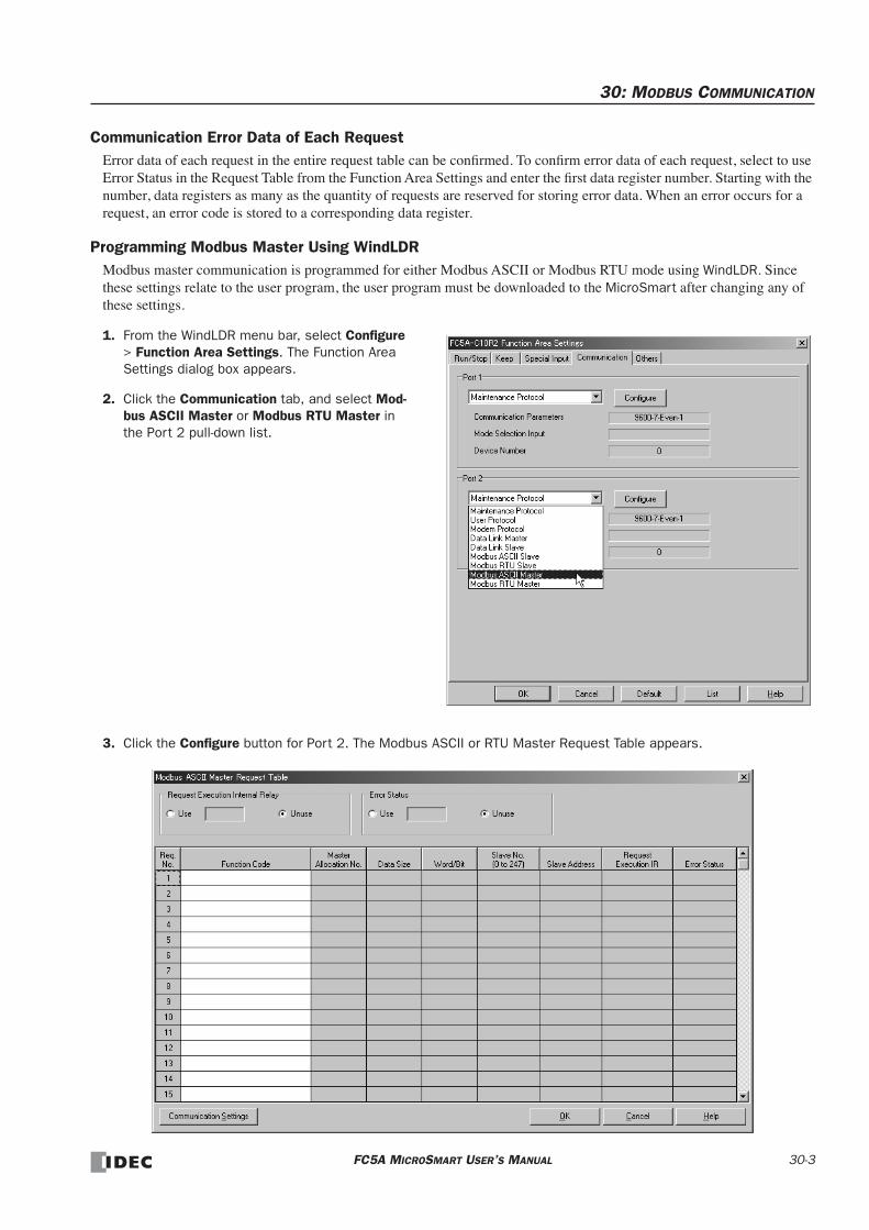
30: MODBUS COMMUNICATION
Communication Error Data of Each RequestError data of each request in the entire request table can be confirmed. To confirm error data of each request, select to use Error Status in the Request Table from the Function Area Settings and enter the first data register number. Starting with the number, data registers as many as the quantity of requests are reserved for storing error data. When an error occurs for a request, an error code is stored to a corresponding data register.
Programming Modbus Master Using WindLDRModbus master communication is programmed for either Modbus ASCII or Modbus RTU mode using WindLDR. Since these settings relate to the user program, the user program must be downloaded to the MicroSmart after changing any of these settings.
1. From the WindLDR menu bar, select Configure > Function Area Settings. The Function Area Settings dialog box appears.
2. Click the Communication tab, and select Mod-bus ASCII Master or Modbus RTU Master in the Port 2 pull-down list.
3. Click the Configure button for Port 2. The Modbus ASCII or RTU Master Request Table appears.
FC5A MICROSMART USER’S MANUAL 30-3

30: MODBUS COMMUNICATION
4. Click the Communication Settings button. The Communication Parameters dialog box appears. Change settings, if required.
5. Click the OK button to return to the Modbus ASCII or RTU Master Request Table. Designate requests under the Function Code. A maximum of 255 requests can be entered in one request table.
Choose to use Request Execution Internal Relays and Error Status data registers. When using Request Execution Internal Relays and Error Status data registers, enter the first number of the operands.
Notes for Editing the Request TableRequest execution internal relays and error status data registers are allocated in the order of request numbers. When deleting a request or changing the order of requests, the relationship of the request to the request execution internal relays and error status data register is changed. If the internal relay or data register is used in the user program, the operand numbers must be changed accordingly. After completing the changes, download the user program again.
6. When editing the Master Request Table is complete, click the OK button to save changes.
7. After closing the Master Request Table, edit a user program for special data register D8054 (transmission wait time) and error detection.
8. Download the user program to the CPU module.
Now, programming for the Modbus master is complete. Details about parameters and valid values are as follows.
Baud Rate (bps) 9600, 19200, 38400, 57600
Parity Even, Odd, None
Stop Bits 1 or 2
Retry Cycle 1 to 10
Receive Timeout 1 to 255 (×10 ms)
30-4 FC5A MICROSMART USER’S MANUAL
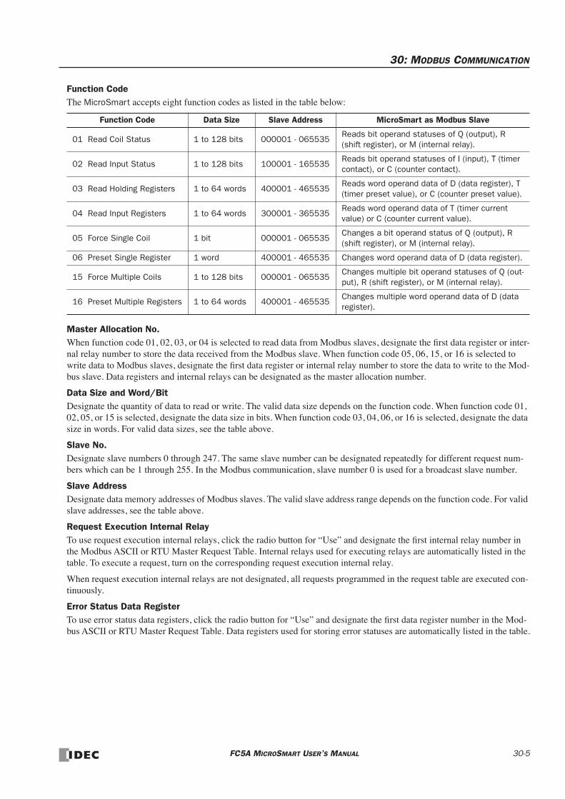
30: MODBUS COMMUNICATION
Function CodeThe MicroSmart accepts eight function codes as listed in the table below:
Master Allocation No.When function code 01, 02, 03, or 04 is selected to read data from Modbus slaves, designate the first data register or inter-nal relay number to store the data received from the Modbus slave. When function code 05, 06, 15, or 16 is selected to write data to Modbus slaves, designate the first data register or internal relay number to store the data to write to the Mod-bus slave. Data registers and internal relays can be designated as the master allocation number.
Data Size and Word/BitDesignate the quantity of data to read or write. The valid data size depends on the function code. When function code 01, 02, 05, or 15 is selected, designate the data size in bits. When function code 03, 04, 06, or 16 is selected, designate the data size in words. For valid data sizes, see the table above.
Slave No.Designate slave numbers 0 through 247. The same slave number can be designated repeatedly for different request num-bers which can be 1 through 255. In the Modbus communication, slave number 0 is used for a broadcast slave number.
Slave AddressDesignate data memory addresses of Modbus slaves. The valid slave address range depends on the function code. For valid slave addresses, see the table above.
Request Execution Internal RelayTo use request execution internal relays, click the radio button for “Use” and designate the first internal relay number in the Modbus ASCII or RTU Master Request Table. Internal relays used for executing relays are automatically listed in the table. To execute a request, turn on the corresponding request execution internal relay.
When request execution internal relays are not designated, all requests programmed in the request table are executed con-tinuously.
Error Status Data RegisterTo use error status data registers, click the radio button for “Use” and designate the first data register number in the Mod-bus ASCII or RTU Master Request Table. Data registers used for storing error statuses are automatically listed in the table.
Function Code Data Size Slave Address MicroSmart as Modbus Slave
01 Read Coil Status 1 to 128 bits 000001 - 065535Reads bit operand statuses of Q (output), R (shift register), or M (internal relay).
02 Read Input Status 1 to 128 bits 100001 - 165535Reads bit operand statuses of I (input), T (timer contact), or C (counter contact).
03 Read Holding Registers 1 to 64 words 400001 - 465535Reads word operand data of D (data register), T (timer preset value), or C (counter preset value).
04 Read Input Registers 1 to 64 words 300001 - 365535Reads word operand data of T (timer current value) or C (counter current value).
05 Force Single Coil 1 bit 000001 - 065535Changes a bit operand status of Q (output), R (shift register), or M (internal relay).
06 Preset Single Register 1 word 400001 - 465535 Changes word operand data of D (data register).
15 Force Multiple Coils 1 to 128 bits 000001 - 065535Changes multiple bit operand statuses of Q (out-put), R (shift register), or M (internal relay).
16 Preset Multiple Registers 1 to 64 words 400001 - 465535Changes multiple word operand data of D (data register).
FC5A MICROSMART USER’S MANUAL 30-5

30: MODBUS COMMUNICATION
Processing RequestsThe data for Modbus communication are processed between the master and slaves as shown below.
Bit Data at Slaves (Function Codes 01, 02, 05, and 15)
• Master Allocation Number: Internal Relay
• Master Allocation Number: Data Register
Word Data at Slaves (Function Codes 03, 04, 06, and 16)
• Master Allocation Number: Internal Relay
• Master Allocation Number: Data Register
Bit +0
Master
Bit +1
Bit +2
Internal Relay (M)
Bit +0
Slave
Bit +1
Bit +2
Modbus Address
Word +0 b15
Master
Word +1
Word +2
Data Register (D)
b14 . . . b1 b0 Bit +0
Slave
Bit +1
Bit +2
Modbus Addr
ess
b2
b15
b14
. . . b1 b0 b2
b15
b14
. . . b1 b0 b2
Bit +0 +15
Master
Bit +16
Bit +32
Internal Relay (M)
+14 . . . +1 +0 W or d +0
Slave
W
or
d +1
W
or
d +2
Modbus Addr
ess
+2
+31
+30
. . . +17 +16 +18
+47
+46
. . . +33 +32 +34
Word +0 b15
Master
Word +1
Word +2
Data Register (D)
b14 . . . b1 b0 W or d +0
Slave
W
or
d +1
W
or
d +2
Modbus Addr
ess
b2
b15
b14
. . . b1 b0 b2
b15
b14
. . . b1 b0 b2
30-6 FC5A MICROSMART USER’S MANUAL

30: MODBUS COMMUNICATION
Operand Allocation Numbers for Modbus Master
Special internal relays and special data re
gisters are allocated to Modbus master communication as shown below.
Special Inter
nal Relay Allocation Numbers
Special Data Register Allocation Numbers
Allocation No.
Description
R/W
M8005
Communication Er
ror
When a communication er
ror occurs, communication error special internal relay M8005 turns on for 1 scan time immediately after the error. Communication error occurs when communica-tion failure has repeated more than the designated retry cycles or when the master station does not receive response within the designated receive timeout period. When a communica-tion error occurs, the request is canceled and the next request is transmitted.The completed request number and error code are stored to special data register D8053.
R
M8080
Modbus Communication Completion Relay
Immediately after a r
equest communication has been completed, Modbus communication completion relay M8080 turns on for 1 scan time. Similarly, when an error occurs, M8080 turns on for 1 scan time. At the same time, the completed request number and error code are stored to special data register D8053.
R
Allocation No.
Description
R/W
D8053
Modbus Communication Er
ror Code
When a Modbus communication is completed, the r
equest number and error code are stored.
High-order byte: Request No.1 to 255
Low-order byte: Error code00h: Normal completion01h: Function error02h: Access destination error (address out of range, address+operand quantity out of range)03h: Operand quantity error, 1-bit write data error11h: ASCII code error (ASCII mode only)12h: Frame length error13h: BCC error14h: Slave number error16h: Timeout error
R
D8054 Modbus Communication T
ransmission Wait Time
When the Micr oSmart sends communication, transmission wait time can be designated by storing a wait time value to D8054. Valid values are 1 through 5000 in milliseconds.
R/W
D8069-D8099
Er
ror Station Number and Error Code
When a communication er
ror occurs in the Modbus communication, the slave number (high-order byte) and error code (low-order byte) are stored to these data registers. Error codes are the same as D8053. When the CPU module is powered up, these data registers are cleared.
R
FC5A MICROSMART USER’S MANUAL 30-7
30: MODBUS COMMUNICATION
Modbus Slave Communication
Modb
us slave communication is made possible by selecting Modbus ASCII Slave or Modbus RTU Slave for port 2 in the
W
indLDR
Function
Area Settings. When a Modbus slave receives a request from the Modbus master, the Modbus slave reads or writes data according to the request. The request is processed at the END processing of the user program.
Modbus Slave Communication Specifi
cations
*1:
D8054 is a special data r
egister for Modbus communication transmission wait time (
×
1 ms). 0 designates 1 ms, and
5000 or mor
e designates 5000 ms. Using D8054 can delay transmission fr
om the Micr
oSmar
t.
*2:
When timeout occurs, the Micr
oSmar
t discar
ds the r
eceived data and waits for the fi
rst frame of the next valid commu
-
nication.
*3:
ASCII mode fi
nds the beginning of a frame by the “:” code. While the
Micr
oSmar
t
is r
eceiving an incoming r
equest mes
-
sage and at the same time r
eceives a “:” code, the
Micr
oSmar
t
discar
ds the r
eceived data and waits for a slave num
-
ber
.
*4:
For communication at 57600 bps, space between frames needs to be a minimum of 1.0 ms.
Communication Completion and Communication ErrorModbus communication finishes when a read or write process is completed successfully or when a communication error occurs. Immediately after a request communication has been completed, Modbus communication completion relay M8080 turns on for 1 scan time. At the same time, the error code is stored to special data register D8053. The data in D8053 is valid only for the 1 scan time when M8080 is on.
When a communication error occurs, communication error special internal relay M8005 also turns on for 1 scan time immediately after the error.
Mode ASCII Mode RTU Mode
Baud Rate (bps) 9600, 19200, 38400, 57600 9600, 19200, 38400, 57600
Data Bits 7 bits (fixed) 8 bits (fixed)
Stop bits 1, 2 bits 1, 2 bits
Parity Odd, even, none Odd, even, none
Slave Number 1 to 31 1 to 31
Response Time *1 1 to 5000 ms (in increments of 1 ms)
1 to 5000 ms (in increments of 1 ms)
Timeout between Characters *2 —*3 1.5 characters minimum
Timeout between Frames *2 —*3 3.5 characters minimum *4
30-8 FC5A MICROSMART USER’S MANUAL

30: MODBUS COMMUNICATION
Address Map
*1: Addresses generally used for Modbus communication. Calculation method of Modbus addresses for MicroSmart operands are described below.
*2: These 4-digit addresses are used in the communication frame. To calculate the address used in communication frame, extract lower 5 digits of the Modbus address, subtract 1 from the value, and conver t the result into hexadecimal.
*3: These operand numbers represent the slim type CPU module. For the operand numbers of the all-in-one type CPU modules, see page 6-1.
Calculating Modbus Addresses for MicroSmart Operands
Modbus Device Name
Modbus Address Map (Decimal) *1
Communication Frame Address *2 MicroSmart Operand *3 Applicable
Function Code
Coil (000000 and above)
000001 - 000504 0000 - 01F7 Q0 - Q627
1, 5, 15000701 - 000956 02BC - 03BB R0 - R255
001001 - 003048 03E8 - 07F7 M0 - M2557
009001 - 009256 2328 - 2427 M8000 - M8317
Input Relay (100000 and above)
100001 - 100504 0000 - 01F7 I0 - I627
2101001 - 101256 03E8 - 04E7 T0 - T255 (timer contact)
101501 - 101756 05DC - 06DB C0 - C255 (counter contact)
Input Register (300000 and above)
300001 - 300256 0000 - 00FF T0 - T255 (timer current value)4
300501 - 300756 01F4 - 02F3 C0 - C255 (counter current value)
Holding Register (400000 and above)
400001 - 408000 0000 - 1F3F D0 - D79993, 6, 16
408001 - 408500 1F40 - 2133 D8000 - D8499
409001 - 409256 2328 - 2427 T0 - T255 (timer preset value)3
409501 - 409756 251C - 261B C0 - C255 (counter preset value)
410001 - 450000 2710 -C34F D10000 - D49999 3, 6, 16
MicroSmart Operand Calculating Modbus Address Calculation Example
I, Q, M
Example: M1325
(132 – 0) × 8 + 5 + 1001 = 2062 Modbus address: 2062
2062 – 1 = 2061 = 80Dh Communication frame address: 080Dh
R, T, C, D
Example: D1756
(1756 – 0) + 400001 = 401757 Modbus address: 401757
Extract lower 5 digits → 1757 1757 – 1 = 1756 = 6CDh Communication frame address: 06DCh
Modbus Device Name MicroSmart Operand Minimum Address ➃ Offset ➄
Coil
Q0 - Q627 0 1
R0 - R255 0 701
M0 - M2557 0 1001
M8000 - M8317 8000 9001
Input Relay
I0 - I627 0 100001
T0 - T255 (timer contact) 0 101001
C0 - C255 (counter contact) 0 101501
Input RegisterT0 - T255 (timer current value) 0 300001
C0 - C255 (counter current value) 0 300501
Holding Register
D0 - D7999 0 400001
D8000 - D8499 8000 408001
T0 - T255 (timer preset value) 0 409001
C0 - C255 (counter preset value) 0 409501
D10000 - D49999 10000 410001
M XXX X➁: Octal
➀: Decimal
(➀ – ➃) × 8 + ➁ + ➄
Minimum Offsetaddress
D XXXXX
➂: Decimal
(➂ – ➃) + ➄
Minimum Offsetaddress
FC5A MICROSMART USER’S MANUAL 30-9

30: MODBUS COMMUNICATION
Programming Modbus Slave Using WindLDRModbus slave communication is programmed for either Modbus ASCII or Modbus RTU mode using WindLDR. Since these settings relate to the user program, the user program must be downloaded to the MicroSmart after changing any of these settings.
1. From the WindLDR menu bar, select Configure > Function Area Settings. The Function Area Settings dialog box appears.
2. Click the Communication tab, and select Modbus ASCII Slave or Modbus RTU Slave in the Port 2 pull-down list.
3. Click the Configure button. The Communication Parameters dialog box appears. Change settings, if required.
4. Click the OK button to save changes.
5. After closing the Function Area Settings screen, edit a user program for special data register D8054 (transmission wait time) and error detection.
6. Download the user program to the CPU module.
Now, programming for the Modbus slave is complete. Details about parameters and valid values are as follows.
Baud Rate (bps)
9600192003840057600
Data Bits7 (ASCII mode)8 (RTU mode)
Parity None, Odd, Even
Stop Bits 1 or 2
Slave Number 1 to 31
Modbus RTU SlaveModbus ASCII Slave
30-10 FC5A MICROSMART USER’S MANUAL
30: MODBUS COMMUNICATION
Operand Allocation Numbers for Modbus SlaveSpecial internal relays and special data registers are allocated to Modbus slave communication as shown below.
Special Internal Relay Allocation Numbers
Special Data Register Allocation Numbers
Allocation No. Description R/W
M8005
Communication ErrorWhen a communication error occurs, communication error special internal relay M8005 turns on for 1 scan time immediately after the error.The error code is stored to special data register D8053.
R
M8080
Modbus Communication Completion RelayImmediately after a request communication has been completed, Modbus communication completion relay M8080 turns on for 1 scan time. Similarly, when an error occurs, M8080 turns on for 1 scan time. At the same time, the error code is stored to special data register D8053.
R
Allocation No. Description R/W
D8053
Modbus Communication Error CodeWhen a Modbus communication error occurs, an error code is stored.
01h: Function error02h: Access destination error (address out of range, address+operand quantity out of range)03h: Operand quantity error, 1-bit write data error11h: ASCII code error (ASCII mode only)12h: Frame length error13h: BCC error
R
D8054Modbus Communication Transmission Wait TimeWhen the MicroSmart sends communication, transmission wait time can be designated by storing a wait time value to D8054. Valid values are 1 through 5000 in milliseconds.
R/W
FC5A MICROSMART USER’S MANUAL 30-11

30: MODBUS COMMUNICATION
Communication ProtocolThis section describes the communication frame format used for Modbus communication. ASCII mode and RTU mode use different communication frame formats.
Communication Frame Format
• ASCII ModeRequest from Modbus Master
ACK Reply from Modbus Slave
NAK Reply from Modbus Slave
• RTU ModeRequest from Modbus Master
ACK Reply from Modbus Slave
NAK Reply from Modbus Slave
Note: Idle means no data flowing on the communication line.
Communication Frame FormatASCII mode finds the beginning of a frame by the “:” code. While the MicroSmart is receiving an incoming request mes-sage and at the same time receives a “:” code, the MicroSmart discards the received data and waits for a slave number.
RTU mode requires a minimum of 3.5-character-long idle time between frames to determine the beginning of a frame. The MicroSmart Modbus master sends requests at idle intervals of 5 ms, which can be changed by storing a required value to special data register D8054.
Slave No.The MicroSmart can be assigned slave numbers 1 through 31. In the 1:1 communication using RS232C, the same slave number must be set in the master and the MicroSmart.
Slave No. 0 is reserved for broadcast slave number and is used to clear all operand data in the slave, or the MicroSmart. In this case, the MicroSmart does not send a reply to the master.
“:” Slave No. Function Code Data LRC CR LF
1 byte 2 bytes 2 bytes 2 bytes 2 bytes
“:” Slave No. Function Code Data LRC CR LF
1 byte 2 bytes 2 bytes 2 bytes 2 bytes
“:” Slave No.Function Code
+ 80HError Code LRC CR LF
1 byte 2 bytes 2 bytes 2 bytes 2 bytes 2 bytes
Idle3.5 characters
Slave No. Function Code Data CRC Idle3.5 characters
1 byte 1 byte 2 bytes
Idle3.5 characters
Slave No. Function Code Data CRC Idle3.5 characters
1 byte 1 byte 2 bytes
Idle3.5 characters
Slave No.Function Code
+ 80HError Code CRC Idle
3.5 characters1 byte 1 byte 1 byte 2 bytes
30-12 FC5A MICROSMART USER’S MANUAL
30: MODBUS COMMUNICATION
LRC and CRCASCII mode uses LRC check codes and RTU mode uses CRC check codes.
• Modbus ASCII Mode — Calculating the LRC (longitudinal redundancy check)Calculate the BCC using LRC for the range from the slave number to the byte immediately before the BCC.
1. Convert the ASCII characters in the range from the slave number to the byte immediately before the BCC, in units of two characters, to make 1-byte hexadecimal data. (Example: 37h, 35h → 75h)
2. Add up the results of step 1.
3. Invert the result bit by bit, and add 1 (2’s complement).
4. Convert the lowest 1-byte data to ASCII characters. (Example: 75h → 37h, 35h)
5. Store the two digits to the BCC (LRC) position.
• Modbus RTU Mode — Calculating the CRC-16 (cyclic redundancy checksum)Calculate the BCC using CRC-16 for the range from the slave number to the byte immediately before the BCC. The gen-eration polynomial is: X16 + X15 + X2 + 1.
1. Take the exclusive OR (XOR) of FFFFh and the first 1-byte data at the slave number.
2. Shift the result by 1 bit to the right. When a carry occurs, take the exclusive OR (XOR) of A001h, then go to step 3. If not, directly go to step 3.
3. Repeat step 2, shifting 8 times.
4. Take the exclusive OR (XOR) of the result and the next 1-byte data.
5. Repeat step 2 through step 4 up to the byte immediately before the BCC.
6. Swap the higher and lower bytes of the result of step 5, and store the resultant CRC-16 to the BCC (CRC) position. (Example: 1234h → 34h, 12h)
FC5A MICROSMART USER’S MANUAL 30-13

30: MODBUS COMMUNICATION
Communication FormatThis section describes the communication format for each function code from the slave number up to immediately before the check code.
Function Code 01 (Read Coil Status) and Function Code 02 (Read Input Status)Function code 01 reads bit operand statuses of Q (output), R (shift register), or M (internal relay). One through 128 con-secutive bits can be read out.
Function code 02 reads bit operand statuses of I (input), T (timer contact), or C (counter contact). One through 128 consec-utive bits can be read out.
Communication FrameRequest from Modbus Master
ACK Reply from Modbus Slave
NAK Reply from Modbus Slave
Communication Example
• ASCII Mode
• RTU Mode
Slave No. Function Code Address No. of Bits
xxh 01h / 02h xxxxh xxxxh
Slave No. Function CodeQuantity of
DataFirst 8 Bits Second 8 Bits Last 8 Bits
xxh 01h / 02h xxh xxh xxh xxh
Slave No. Function Code Error Code
xxh 81h / 82h xxh
Purpose
Read 15 bits starting at output Q10.
Q10 → (1 – 0) × 8 + 0 + 1 = 9Modbus address: 9
9 – 1 = 8 = 8hCommunication frame address: 0008h
ConditionSlave No. 8Q10 through Q26 binary data: 1234h
Request from Modbus Master ‘:’ 3038 3031 30303038 30303046 (LRC) CRLF
ACK Reply from Modbus Slave ‘:’ 3038 3031 3032 3334 3132 (LRC) CRLF
NAK Reply from Modbus Slave ‘:’ 3038 3831 xxxx (LRC) CRLF
Request from Modbus Master 08 01 0008 000F (CRC)
ACK Reply from Modbus Slave 08 01 02 34 12 (CRC)
NAK Reply from Modbus Slave 08 81 xx (CRC)
30-14 FC5A MICROSMART USER’S MANUAL

30: MODBUS COMMUNICATION
Function Code 03 (Read Holding Registers) and Function Code 04 (Read Input Registers)Function code 03 reads word operand data of D (data register), T (timer preset value), or C (counter preset value). One through 64 consecutive words can be read out.
Function code 04 reads word operand data of T (timer current value) or C (counter current value). One through 64 consec-utive words can be read out.
Communication FrameRequest from Modbus Master
ACK Reply from Modbus Slave
NAK Reply from Modbus Slave
• Communication Example
• ASCII Mode
• RTU Mode
Slave No. Function Code Address No. of Words
xxh 03h / 04h xxxxh xxxxh
Slave No. Function CodeQuantity of
DataFirst High Byte First Low Byte Last Low Byte
xxh 03h / 04h xxh xxh xxh xxh
Slave No. Function Code Error Code
xxh 83h / 84h xxh
Purpose
Read 2 words starting at data register D1710.
D1710 → (1710 – 0) + 400001 = 401711Modbus address: 401711
Extract lower 5 digits → 17111711 – 1 = 1710 = 6AEhCommunication frame address: 06AEh
ConditionSlave No. 8D1710 data: 1234hD1711 data: 5678h
Request from Modbus Master ‘:’ 3038 3033 30364145 30303032 (LRC) CRLF
ACK Reply from Modbus Slave ‘:’ 3038 3033 3034 3132 3334 3536 3738 (LRC) CRLF
NAK Reply from Modbus Slave ‘:’ 3038 3833 xxxx (LRC) CRLF
Request from Modbus Master 08 03 06AE 0002 (CRC)
ACK Reply from Modbus Slave 08 03 04 12 34 56 78 (CRC)
NAK Reply from Modbus Slave 08 83 xx (CRC)
FC5A MICROSMART USER’S MANUAL 30-15

30: MODBUS COMMUNICATION
Function Code 05 (Force Single Coil)Function code 05 changes a bit operand status of Q (output), R (shift register), or M (internal relay).
Communication FrameRequest from Modbus Master
ACK Reply from Modbus Slave
NAK Reply from Modbus Slave
Communication Example
• ASCII Mode
• RTU Mode
Slave No. Function Code AddressOFF: 0000HON: FF00H
xxh 05h xxxxh xxxxh
Slave No. Function Code AddressOFF: 0000HON: FF00H
xxh 05h xxxxh xxxxh
Slave No. Function Code Error Code
xxh 85h xxh
Purpose
Force internal relay M1320 on.
M1320 → (132 – 0) × 8 + 0 + 1001 = 2057Modbus address: 2057
2057 – 1 = 2056 = 808hCommunication frame address: 0808h
Condition Slave No. 8
Request from Modbus Master ‘:’ 3038 3035 30383038 46463030 (LRC) CRLF
ACK Reply from Modbus Slave ‘:’ 3038 3035 30383038 46463030 (LRC) CRLF
NAK Reply from Modbus Slave ‘:’ 3038 3835 xxxx (LRC) CRLF
Request from Modbus Master 08 05 0808 FF00 (CRC)
ACK Reply from Modbus Slave 08 05 0808 FF00 (CRC)
NAK Reply from Modbus Slave 08 85 xx (CRC)
30-16 FC5A MICROSMART USER’S MANUAL

30: MODBUS COMMUNICATION
Function Code 06 (Preset Single Register)Function code 06 changes word operand data of D (data register).
Communication FrameRequest from Modbus Master
ACK Reply from Modbus Slave
NAK Reply from Modbus Slave
Communication Example
• ASCII Mode
• RTU Mode
Slave No. Function Code Address New Data
xxh 06h xxxxh xxxxh
Slave No. Function Code AddressAcknowledge
Data
xxh 06h xxxxh xxxxh
Slave No. Function Code Error Code
xxh 86h xxh
Purpose
Write 8000 to data register D1708.
D1708 → (1708 – 0) + 400001 = 401709Modbus address: 401709
Extract lower 5 digits → 17091709 – 1 = 1708 = 6AChCommunication frame address: 06ACh
Condition Slave No. 8
Request from Modbus Master ‘:’ 3038 3036 30364143 31463430 (LRC) CRLF
ACK Reply from Modbus Slave ‘:’ 3038 3036 30364143 31463430 (LRC) CRLF
NAK Reply from Modbus Slave ‘:’ 3038 3836 xxxx (LRC) CRLF
Request from Modbus Master 08 06 06AC 1F40 (CRC)
ACK Reply from Modbus Slave 08 06 06AC 1F40 (CRC)
NAK Reply from Modbus Slave 08 86 xx (CRC)
FC5A MICROSMART USER’S MANUAL 30-17

30: MODBUS COMMUNICATION
Function Code 15 (Force Multiple Coils)Function code 15 changes bit operand statuses of Q (output), R (shift register), or M (internal relay). One through 128 con-secutive bits can be changed.
Communication FrameRequest from Modbus Master
ACK Reply from Modbus Slave
NAK Reply from Modbus Slave
Communication Example
• ASCII Mode
• RTU Mode
Slave No.Function
CodeAddress
No. of Bits
Quantity of Data
First 8 Bits
Second 8 Bits
Last 8 Bits
xxh 0Fh xxxxh xxxxh xxh xxh xxh xxh
Slave No. Function Code Address No. of Bits
xxh 0Fh xxxxh xxxxh
Slave No. Function Code Error Code
xxh 8Fh xxh
Purpose
Write the following bit statuses to internal relays M605 through M624.M605 M606 M607 (ON) (0N) (OFF)
M610 M611 M612 M613 M614 M615 M616 M617 (ON) (OFF) (ON) (ON) (OFF) (OFF) (0N) (OFF)
M620 M621 M622 M623 M624 (OFF) (OFF) (OFF) (OFF) (OFF)
M605 (LSB) through M614 (MSB) binary data: 6BM615 (LSB) through M624 (MSB) binary data: 02
M605 → (60 – 0) × 8 + 5 + 1001 = 1486Modbus address: 1486
1486 – 1 = 1485 = 5CDhCommunication frame address: 05CDh
Condition Slave No. 8
Request from Modbus Master ‘:’ 3038 3046 30354344 30303130 3032 3642 3032 (LRC) CRLF
ACK Reply from Modbus Slave ‘:’ 3038 3046 30354344 30303130 (LRC) CRLF
NAK Reply from Modbus Slave ‘:’ 3038 3846 xxxx (LRC) CRLF
Request from Modbus Master 08 0F 05CD 0010 02 6B 02 (CRC)
ACK Reply from Modbus Slave 08 0F 05CD 0010 (CRC)
NAK Reply from Modbus Slave 08 8F xx (CRC)
30-18 FC5A MICROSMART USER’S MANUAL

30: MODBUS COMMUNICATION
Function Code 16 (Preset Multiple Registers)Function code 16 changes word operand data of D (data register). One through 64 consecutive words can be changed.
Communication FrameRequest from Modbus Master
ACK Reply from Modbus Slave
NAK Reply from Modbus Slave
Communication Example
• ASCII Mode
• RTU Mode
Slave No.Function
CodeAddress
No. of Words
Quantity of Data
First High Byte
First Low Byte
Last Low Byte
xxh 10h xxxxh xxxxh xxh xxh xxh xxh
Slave No. Function Code Address No. of Words
xxh 10h xxxxh xxxxh
Slave No. Function Code Error Code
xxh 90h xxh
Purpose
Write the following data to four data registers D1708 through D1711.D1708 D1709 D1710 D1711 (1234h) (5678h) (ABCDh) (EF01h)
D1708 → (1708 – 0) + 400001 = 401709Modbus address: 401709
Extract lower 5 digits → 17091709 – 1 = 1708 = 6AChCommunication frame address: 06ACh
Condition Slave No. 8
Request from Modbus Master‘:’ 3038 3130 30364143 30303034 3038 3132 3334 3536 3738 4142 4344 4546 3031 (LRC) CRLF
ACK Reply from Modbus Slave ‘:’ 3038 3130 30364143 30303034 (LRC) CRLF
NAK Reply from Modbus Slave ‘:’ 3038 3930 xxxx (LRC) CRLF
Request from Modbus Master 08 10 06AC 0004 08 12 34 56 78 AB CD EF 01 (CRC)
ACK Reply from Modbus Slave 08 10 06AC 0004 (CRC)
NAK Reply from Modbus Slave 08 90 xx (CRC)
FC5A MICROSMART USER’S MANUAL 30-19

30: MODBUS COMMUNICATION
30-20 FC5A MICROSMART USER’S MANUAL

31: AS-INTERFACE MASTER COMMUNICATION
IntroductionThis chapter describes general information about the Actuator-Sensor-Interface, abbreviated AS-Interface, and detailed information about using the AS-Interface master module.
About AS-InterfaceAS-Interface is a type of field bus that is primarily intended to be used to control sensors and actuators. AS-Interface is a network system that is compatible with the IEC62026 standard and is not proprietary to any one manufacturer. A master device can communicate with slave devices such as sensors, actuators, and remote I/Os, using digital and analog signals transmitted over the AS-Interface bus.
The AS-Interface system is comprised of the following three major components:
• One master, such as the MicroSmart AS-Interface master module (FC4A-AS62M) • One or more slave devices, such as sensors, actuators, switches, and indicators • Dedicated 30V DC AS-Interface power supply (26.5 to 31.6V DC)
These components are connected using a two-core cable for both data transmission and AS-Interface power supply. AS-Interface employs a simple yet efficient wiring system and features automatic slave address assignment function, while installation and maintenance are also very easy.
Applicable Sensors and Actuators for AS-Interface
AS-Interface Compatible Sensors and ActuatorsAS-Interface compatible sensors and actuators communicate using the built-in AS-Interface function, and serve as AS-Interface slaves when connected directly to the AS-Interface bus via a branch unit or a T-junction unit.
Sensors/Actuators Not Compatible with AS-InterfaceConventional sensors and actuators that are not compatible with the AS-Interface can also be connected to the AS-Inter-face bus using a remote I/O slave and be handled in the same way as devices that are compatible with the AS-Interface.
Remote I/O Type SlaveBranch Unit T-junction Unit
AS-Interface Non-compatibleSensors/ActuatorsAS-Interface Compatible Sensors/Actuators
AS-Interface Bus
Maximum I/O points when using one or two AS-Interface master modules
AS-Interface Master Module 1 module 2 modules
Maximum Slaves 62 slaves 124 slaves
Maximum I/O Points 434 (248 inputs / 186 outputs) 868 (496 inputs / 372 outputs)
Maximum Communication Distance
Without repeater: 100m With 2 repeaters: 300m
Without repeater: 100m With 2 repeaters: 300m
FC5A MICROSMART USER’S MANUAL 31-1

31: AS-INTERFACE MASTER COMMUNICATION
AS-Interface System Requirements
MasterThe AS-Interface master controls and monitors the status of slave devices connected to the AS-Interface bus.
Normally, the AS-Interface master is connected to a PLC (sometimes called ‘host’) or a gateway. For example, the Micro-Smart AS-Interface master module is connected to the MicroSmart CPU module.
The FC5A MicroSmart CPU module can be used with one or two AS-Interface master modules, so two separate AS-Inter-face networks can be set up.
The AS-Interface master module can connect a maximum of 62 digital I/O slaves. A maximum of seven analog I/O slaves can also be connected to the AS-Interface master module (compliant with AS-Interface ver. 2.1 and analog slave profile 7.3).
SlavesVarious types of slave devices can be connected to the AS-Interface bus, including sensors, actuators, and remote I/O devices. Analog slaves can also be connected to process analog data.
Slaves are available in standard slaves and A/B slaves. Standard slaves have an address of 1 trough 31 in the standard address range. A/B slaves have an address of 1A through 31A in the standard address range or 1B through 31B in the expanded address range. Among the A/B slaves, slaves with an address of 1A through 31A are called A slaves, and slaves with an address of 1B through 31B are called B slaves.
• The AS-Interface master module cannot be connected to the all-in-one 10-I/O and 16-I/O type CPU modules and the expansion interface module.
• One or two AS-Interface master modules can be connected to the CPU module. If more than two AS-Interface master modules are connected, an error occurs and special data register D8037 (quan-tity of expansion I/O modules) stores error code 40 (hex).
• Normally, a maximum of four expansion I/O modules can be connected to the all-in-one 24-I/O type CPU module. But when one or two AS-Interface master modules are connected, only a total of three expansion modules can be connected, including the AS-Interface master modules. Do not con-nect more than three expansion modules due to the amount of heat generated. If more than three expansion modules, including the AS-Interface master module, are connected, an error occurs and special data register D8037 (quantity of expansion I/O modules) stores error code 20 (hex).
• Similarly, slim type CPU modules can normally connect a maximum of seven expansion I/O mod-ules, but can connect a maximum of six expansion modules including one or two AS-Interface mas-ter modules. If more than six expansion modules, including the AS-Interface master module, are connected, an error occurs and special data register D8037 (quantity of expansion I/O modules) stores error code 20 (hex).
• The AS-Interface master module can connect a maximum of seven analog I/O slaves. When more than seven analog I/O slaves are connected, the AS-Interface system will not operate correctly.
AS-Interface Master Module FC4A-AS62MOne or two AS-Interface master modules can be mounted.Note: The AS-Interface master module can not be mounted to the right of the expansion interface module.
Applicable FC5A MicroSmart CPU Modules
FC5A-C24R2 FC5A-C24R2C FC5A-D16RK1 FC5A-D16RS1
FC5A-D32K3 FC5A-D32S3
Caution
31-2 FC5A MICROSMART USER’S MANUAL

31: AS-INTERFACE MASTER COMMUNICATION
AS-Interface Power SupplyThe AS-Interface bus uses a dedicated 30V DC power supply (AS-Interface power supply), which is indicated with the AS-Interface mark. General-purpose power sup-ply units cannot be used for the AS-Interface bus.
When using two AS-Interface master modules, two AS-Interface power supplies are needed. Since the AS-Interface cable transmits both signals and power, each network requires a separate power supply.
Recommended IDEC AS-Interface Power Supplies
CablesThe AS-Interface bus uses only one cable to transmit signals and power. Use one of the following cable types (the wire does not have to be stranded).
• Standard yellow unshielded AS-Interface cable (with polarity)
• Ordinary two-wire flat cable
Applicable Cable Specifications
Note: When using single wires, the maximum cable length is 200 mm. See “Maximum Communication Distance” on page 31-1.
• Use a VLSV (very low safety voltage) to power the AS-Interface bus. The normal output voltage of the AS-Interface power supply is 30V DC.
Input Voltage Output Voltage Output Wattage Type No.
100 to 240V AC 30.5V DC 73W PS2R-Q30ABL
145W PS2R-F30ABL
Cable Type Cable Size/Manufacturer Cross-sectional View
AS-Interface Standard Cable
Cable sheath color: Yellow Conductor cross section: 1.5 mm2
LAPP’s CablesType No: 2170228 (sheath material EPDM)Type No: 2170230 (sheath material TPE)
2-wire Flat CableorSingle Wires(See Note)
Conductor cross sectionStranded wire: 0.5 to 1.0 mm2
Solid wire: 0.75 to 1.5 mm2
AWG: 20 to 16
AS-Interface Marks
Caution
AS-Interface Cable Two-wire Flat Cable
AS-Interface – AS-Interface + (blue) (brown)
AS-Interface – AS-Interface + (blue) (brown)
FC5A MICROSMART USER’S MANUAL 31-3

31: AS-INTERFACE MASTER COMMUNICATION
Main Features of AS-Interface V2 with Slave Expansion CapabilityThe AS-Interface is a reliable bus management system in which one master periodically monitors each slave device con-nected on the AS-Interface bus in sequence. The master manages the I/O data, parameters, and identification codes of each slave in addition to slave addresses. The management data depends on the type of the slave as follows:
Standard Slaves• A maximum of four inputs and four outputs for each slave• Four parameters for setting a slave’s operation mode (P3, P2, P1, P0)• Four identification codes (ID code, I/O code, ID2 code, and ID1 code)
A/B Slaves• A maximum of four inputs and three outputs for each slave• Three parameters for setting a slave’s operation mode (P2, P1, P0)• Four identification codes (ID code, I/O code, ID2 code, and ID1 code)
Note 1: Parameters P3 through P0 are used to set an operation mode of the slave. For details, see the user’s manual for the slave.
Note 2: The slaves connected to the AS-Interface bus are distinguished from each other by the ID code and I/O code con-tained in each slave. Some slaves have ID2 code and ID1 code to indicate the internal functions of the slave. For example, analog slaves use the ID2 code to represent the channel number of the slave.
Note 3: The MicroSmart AS-Interface master module is also compatible with AS-Interface ver. 2.1 and earlier slaves.
Slave AddressesEach standard slave connected to the AS-Interface bus can be allocated an address of 1 through 31. Each A/B slave can be allocated an address of 1A through 31A or 1B through 31B. All slaves are set to address 0 at factory before shipment. The address of a slave can be changed using the “addressing tool.” Using WindLDR, the addresses of slaves connected to the AS-Interface master modules 1 and 2 can also be changed (see page 31-35).
When a slave fails during operation and needs to be replaced, if the auto addressing function is enabled on the master mod-ule, just replace the slave with a new one (with address 0 and the same identification codes). The new slave will automati-cally be allocated the same address as the slave that was removed, and you do not have to set the address again. For details of the ASI command to enable auto addressing, see page 31-30.
Slave IdentificationSlaves have the following four identification codes. The master checks the identification codes to determine the type and feature of the slave connected on the AS-Interface bus.
ID CodeThe ID code consists of 4 bits to indicate the type of the slave, such as sensor, actuator, standard slave, or A/B slave. For example, the ID code for a standard remote I/O is 0, and that for an A/B slave is A (hex).
I/O CodeThe I/O code consists of 4 bits to indicate the quantity and allocation of I/O points on a slave.
I: input, O: output, B: input and output
ID2 CodeThe ID2 code consists of 4 bits to indicate the internal function of the slave.
ID1 CodeThe ID1 code consists of 4 bits to indicate additional identification of the slave. Standard slaves can have an ID1 code of 0000 through 1111 (bin). A/B slaves use the MSB to indicate A or B slave, and can have a unique value only for the lower three bits. The MSB of A slaves is set to 0, and that of B slaves is set to 1.
I/O Code Allocation I/O Code Allocation I/O Code Allocation I/O Code Allocation0h I, I, I, I 4h I, I, B, B 8h O, O, O, O Ch O, O, B, B1h I, I, I, O 5h I, O, O, O 9h O, O, O, I Dh O, I, I, I2h I, I, I, B 6h I, B, B, B Ah O, O, O, B Eh O, B, B, B3h I, I, O, O 7h B, B, B, B Bh O, O, I, I Fh (reserved)
31-4 FC5A MICROSMART USER’S MANUAL

31: AS-INTERFACE MASTER COMMUNICATION
Quantities of Slaves and I/O PointsThe quantity of slaves that can be connected to one AS-Interface master module is as follows.
• Standard slaves: 31 maximum
• A/B slaves: 62 maximum
The limits for slave quantities given above apply when the slaves are either all standard slaves or are all A/B slaves.
When 62 A/B slaves (with four inputs and three outputs) are connected, a maximum of 434 I/O points (248 inputs and 186 outputs) can be controlled by one AS-Interface master module.
When using a mix of standard slaves and A/B slaves together, the standard slaves can only use addresses 1(A) through 31(A). Also, when a standard slave takes a certain address, the B address of the same number cannot be used for A/B slaves.
AS-Interface Bus Topology and Maximum LengthThe AS-Interface bus topology is flexible, and you can wire the bus freely according to your requirements.
When repeaters or extenders are not used, the bus length can be 100m (328 feet) at the maximum.
The FC4A-AS62M AS-Interface master module can use two repeaters to extend the bus length to 300m.
AS-Interface Bus Cycle TimeThe AS-Interface bus cycle time is the amount of time required for a master to cycle through every slave on the bus.
The information for each slave is continuously transmitted over the bus in sequence, so the AS-Interface bus cycle time depends on the quantity of active slaves.
• When up to 19 slaves are active, the bus cycle time is 3 ms.
• When 20 to 62 slaves are active, the bus cycle time is 0.156 × (1+N) ms where N is the number of slaves.
When A slave and B slave have the same address number (e.g. 12A and 12B), the two slaves are alternately updated each cycle. Therefore, when the system consists of 31 A slaves and 31 B slaves, then the AS-Interface bus cycle time will be 10 ms.
Maximum AS-Interface Bus Cycle Time
• When 31 slaves are connected, the maximum bus cycle time is 5 ms.
• When 62 slaves are connected, the maximum bus cycle time is 10 ms.
High Reliability and SecurityThe AS-Interface employs a transfer process of high reliability and high security. The master monitors the AS-Interface power supply voltage and data transmitted on the bus, and detects slave failures and data errors.
Even when a slave is replaced or a new slave is added during operation, the AS-Interface master module need not be shut down and can continue uninterrupted communication with other active slaves on the bus.
FC5A MICROSMART USER’S MANUAL 31-5

31: AS-INTERFACE MASTER COMMUNICATION
Operation BasicsThis section describes simple operating procedures for the basic AS-Interface system from programming WindLDR on a computer to monitoring the slave operation.
AS-Interface System SetupThe sample AS-Interface system consists of the following devices:
AS-Interface Cable WiringBefore wiring the AS-Interface cable, remove the AS-Interface cable terminal block from the AS-Interface cable connector on the AS-Interface master module.
AS-Interface specifies use of brown cables for the AS-Interface + line, and blue cables for the AS-Interface – line. Connect the cables to match the color labels on the terminal block. Tighten the terminal screws to a torque of 0.5 to 0.6 N·m.
Insert the terminal block to the connector on the AS-Interface master module, and tighten the mounting screws to a torque of 0.3 to 0.5 N·m.
Name Type No. Description
FC5A MicroSmart Slim Type CPU Module FC5A-D16RK1 —
MicroSmart AS-Interface Master Module FC4A-AS62M —
WindLDR FC9Y-LP2CDW Version 5.0 or higher
AS-Interface Standard Slave —1 unitAddress 0ID: 0, I/O: 7, ID2: F, ID1: 7
AS-Interface Power Supply PS2R-Q30ABL Output 30.5V DC, 2.4A (73W)
Slim Type CPU Module FC5A-D16RK1
AS-Interface Master Module FC4A-AS62M
Standard AS-Interface Cable
Computer Link Cable 4C FC2A-KC4C 3m (9.84 ft.) long
AS-Interface Power Supply
Standard SlaveAddress 0ID: 0, I/O: 7, ID2: F, ID1: 7
Blue AS-Interface –
Use a ferrule.
Brown AS-Interface +
Use a ferrule. Blue Label
Brown Label
31-6 FC5A MICROSMART USER’S MANUAL

31: AS-INTERFACE MASTER COMMUNICATION
Power Supply
Power Supply Wiring DiagramA recommended power supply wiring diagram is shown below. Use a common power switch for both the CPU module power supply and AS-Interface power supply to make sure that both power supplies are turned on and off at the same time.
Note: A failed slave can be replaced with a new slave with address 0 without turning off the power to the CPU module and the AS-Interface line. But, if power has been turned off before replacing the slaves, install a new slave with address 0 and take one of the following steps, because the AS-Interface master module has to be initialized to enable communication.
• Disconnect the AS-Interface cable connector and turn on both power supplies. Five seconds later, connect the AS-Interface cable connector.
• Turn on the CPU module power supply first. Five seconds later, turn on the AS-Interface power supply.
• When turning off the power to the CPU module, also turn off the AS-Interface power supply. If the CPU module is powered down and up while the AS-Interface power remains on, AS-Interface com-munication may stop due to a configuration error, resulting in a communication error.
• Turn on the AS-Interface power supply no later than the CPU module power supply, except when slave address 0 exists on the network. The two power supplies may be turned off in any order.
• Immediately after power-up, the CPU module cannot access slave I/O data in the AS-Interface mas-ter module. Make the user program so that slave I/O data are accessed after special internal relay M1945 (Normal_Operation_Active) has turned on. See page 31-25.
Caution
AS-Interface Power Supply30V DC
Slim Type CPU Module FC5A-D32K3
AS-Interface Master Module FC4A-AS62M
Slave 1
Slave 2
AC Power
CPU Module Power Supply24V DC
Power Switch
AS-Interface Power Switch (Note)
AS-Interface Cable Connector
VLSV (very low safety voltage)
FC5A MICROSMART USER’S MANUAL 31-7
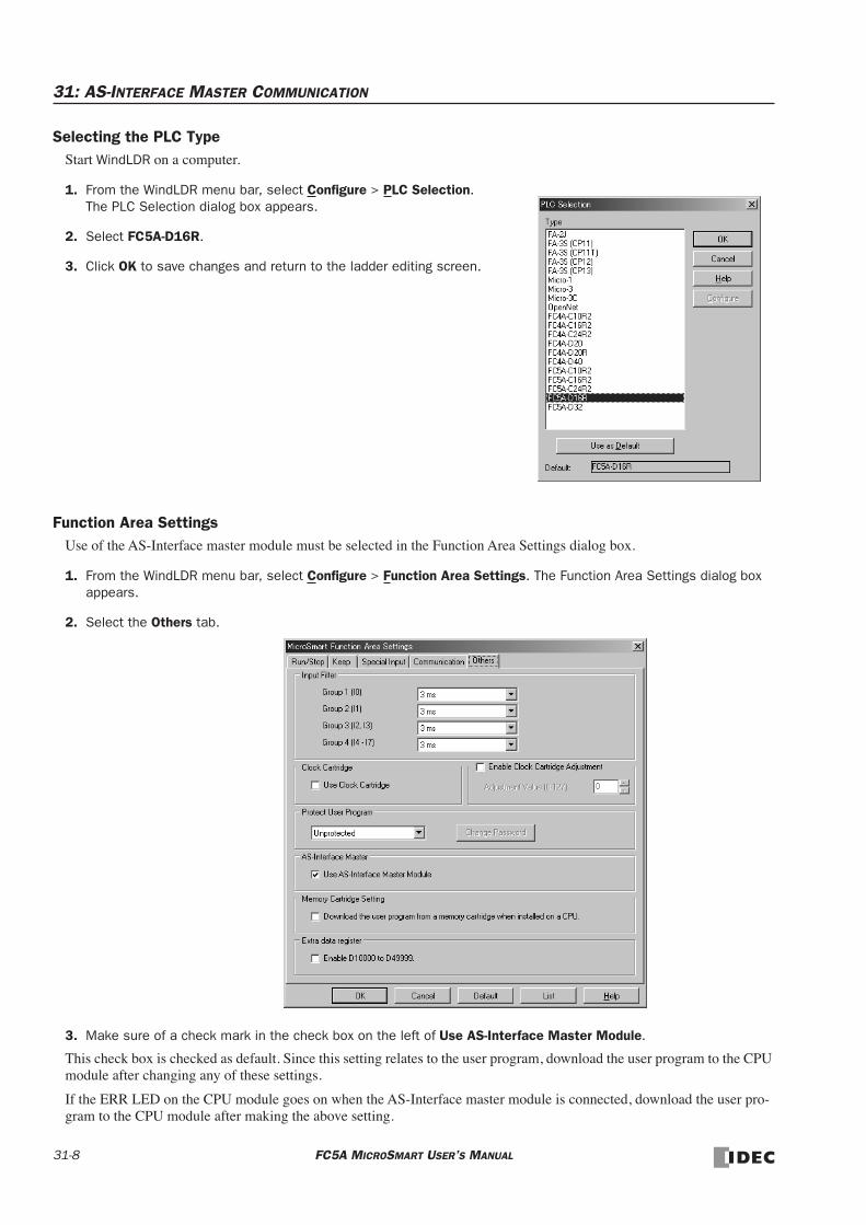
31: AS-INTERFACE MASTER COMMUNICATION
Selecting the PLC TypeStart WindLDR on a computer.
1. From the WindLDR menu bar, select Configure > PLC Selection. The PLC Selection dialog box appears.
2. Select FC5A-D16R.
3. Click OK to save changes and return to the ladder editing screen.
Function Area SettingsUse of the AS-Interface master module must be selected in the Function Area Settings dialog box.
1. From the WindLDR menu bar, select Configure > Function Area Settings. The Function Area Settings dialog box appears.
2. Select the Others tab.
3. Make sure of a check mark in the check box on the left of Use AS-Interface Master Module.
This check box is checked as default. Since this setting relates to the user program, download the user program to the CPU module after changing any of these settings.
If the ERR LED on the CPU module goes on when the AS-Interface master module is connected, download the user pro-gram to the CPU module after making the above setting.
31-8 FC5A MICROSMART USER’S MANUAL

31: AS-INTERFACE MASTER COMMUNICATION
Assigning a Slave AddressAS-Interface compatible slave devices are set to address 0 at factory. Connect the slave to the AS-Interface master module as shown on page 31-6. Do not connect two or more slaves with slave address 0, otherwise the AS-Interface master module cannot recognize slave addresses correctly.
1. Power up the MicroSmart CPU module first. Approximately 5 seconds later, turn on the AS-Interface power supply.
Note: When slave address 0 is not mounted on the AS-Interface bus, the CPU module power supply and the AS-Interface power supply can be turned on at the same time. See page 31-7.
2. From the WindLDR menu bar, select Configure > AS-Interface Master to open the Configure AS-Interface Master dialog box. Press Refresh to collect slave information and update the screen display. (When configuration in the master module is complete, you do not have to press Refresh since the screen display is updated automatically.)
On the Configure AS-Interface Master dialog box, slave address 0 is shaded with yellow. This means that the master mod-ule has found slave address 0 on the AS-Interface bus. The CDI for address 0 shows 07F7 (ID: 0, I/O: 7, ID2: F, ID1: 7).
3. Click the slave address “00” to open the Change Slave Address dialog box for slave 0. To assign slave address 1 to the slave, enter 1 in the New Address field and click OK.
The new address “01” is shaded with yellow to indicate that the address assignment is complete.
4. When changing slave addresses on other slaves, continue from step 3 if it is possible to wire the slave without turning off power, or from step 1 if the CPU module is shut down.
Yellow Shade
Click slave address 0 to open the Change Slave Address dialog box.
CDI: Configuration Data Image PCD: Permanent Configuration Data
Yellow Shade
FC5A MICROSMART USER’S MANUAL 31-9

31: AS-INTERFACE MASTER COMMUNICATION
Configuring a SlaveNext, you have to set the slave configuration in the AS-Interface master module, either by using pushbuttons PB1 and PB2 on the AS-Interface master module or WindLDR.
Configuration Using Pushbuttons PB1 and PB2
1. Check that PWR LED and CMO LED on the AS-Interface master module are on (normal protected mode).
2. Press pushbuttons PB1 and PB2 together for 3 seconds. CMO LED turns off and LMO LED turns on (protected mode).
3. Press pushbutton PB2 for 3 seconds. CNF LED flashes (configuration mode).
4. About 5 seconds later, press pushbutton PB1 for 3 seconds. All I/O LEDs blink once to complete configuration.
5. Shut down the CPU module and AS-Interface master module, and power up again. Check that FLT LED is off, which indicates that configuration is complete.
6. Use WindLDR to view slave information on the Configure AS-Interface Master dialog box and check that all slaves are recognized correctly.
Press PB1 and PB2. Press PB2. Press PB1.
Shut down andpower up again.
31-10 FC5A MICROSMART USER’S MANUAL

31: AS-INTERFACE MASTER COMMUNICATION
Configuration Using WindLDR
Slave configuration can be set using WindLDR in two ways; using the Auto Configuration or Manual Configuration button on the Configure AS-Interface Master dialog box.
1. Click the Auto Configuration button to store the configuration information (LDS, CDI, PI) of the connected slaves to the EEPROM (LPS, PCD, PP) in the AS-Interface master module. For details, see page 31-36.
The auto configuration automatically stores the information of slaves found on the AS-Interface bus to the EEPROM in the master module, and this completes configuration. Another method of configuration is manual configuration as follows.
2. Click the PCD value “FFFF” of slave address 01 to open the Configure Slave 01A dialog box.
3. Enter the same value as CDI “07F7” in the PCD field. (Set FFFF to PCD values of all unused slaves.)
4. Select initial settings of parameters (PP) P0 through P3, if required.
5. Click the Manual Configuration button to store the selected PCD and parameter values to the master module.
6. Check that the blue shade appears at slave address 01. Now, configuration is complete.
Yellow Shade
Blue Shade
FC5A MICROSMART USER’S MANUAL 31-11

31: AS-INTERFACE MASTER COMMUNICATION
Monitoring Digital I/O, and Changing Output Status and ParametersWhile the MicroSmart is communicating with AS-Interface slaves through the AS-Interface bus, operating status of AS-Interface slaves can be monitored using WindLDR on a computer. Output statuses and parameter image (PI) of slaves con-nected to the AS-Interface master module can also be changed using WindLDR.
1. From the WindLDR menu bar, select Online > Monitor. From the WindLDR menu bar, select Online, and select Monitor AS-Interface Slaves in the pull-down menu. The Monitor AS-Interface Slaves dialog box appears.
Active slaves are indicated with blue shade.
Next step is to change output status of the active slave.
2. Click the output of slave address 01 to open the Slave Status 01A dialog box.
3. Click the On or Off button to change the statuses of outputs O0 through O3 and parameters (PI) P0 through P3 as required.
The selected parameters (PI) are in effect until the CPU module is shut down. When the CPU module is powered up again, the parameter values (PP) selected in the slave configuration procedure (page 31-10) will take effect. To store the changed parameter values to the AS-Interface master module EEPROM, execute the Copy PI to PP command by storing 0306, 0100, 0000, 0000, 0001 to data registers D1941 through D1945. See page 31-30.
Blue Shade
31-12 FC5A MICROSMART USER’S MANUAL

31: AS-INTERFACE MASTER COMMUNICATION
Troubles at System Start-upThe following table summarizes possible troubles at system start-up, probable causes and actions to be taken.
Trouble Cause and Action
PWR LED is off.(power)
• AS-Interface power is not supplied to the AS-Interface master module. Check that wiring is correct and AS-Interface power is supplied.
• Power is not supplied from the CPU module to the AS-Interface master module. Check the connection between the CPU module and the AS-Interface master module.
FLT LED is on.(fault)
• Slave configuration on the bus is incorrect. Use the WindLDR slave monitor function to check that slaves are connected correctly. Perform configuration, if necessary. For the configuration method, see page 31-34.
If FLT LED remains on even though slaves are connected correctly and configuration is completed, either disconnect and reconnect the AS-Interface connector, or turn off and on the AS-Interface power supply.
LMO LED is on.(local mode)
The CPU module fails to communicate with the AS-Interface master module. Check the following points.
• Is the CPU module compatible with AS-Interface? Check the Type No. of the CPU module.
• Is a check mark put in the check box “Use AS-Interface Master Module” in WindLDR Function Area Settings? The box is checked as default. If not, put a check mark and download the user program to the CPU module.
OFF LED is on.(offline)
• While a slave of address 0 was connected, power was turned on. After changing the slave address, power up again. For the address changing method, see page 31-35.
Slave operation is unstable.
• Check if there are two or more slaves with the same address. Each slave must have a unique address. If two slaves have the same address and same identification codes (ID, I/O, ID2, ID1), the AS-Interface master module may fail to detect an error. When changing the duplicate slave address using WindLDR, remove one of the slaves from the bus.
FC5A MICROSMART USER’S MANUAL 31-13

31: AS-INTERFACE MASTER COMMUNICATION
Pushbuttons and LED IndicatorsThis section describes the operation of pushbuttons PB1 and PB2 on the AS-Interface master module to change operation modes, and also explains the functions of address and I/O LED indicators.
Pushbutton OperationThe operations performed by pushbuttons PB1 and PB2 on the front of the AS-Interface master module depend on the duration of being pressed. A “long press” switches the operation mode, and a “short press” switches the slave being moni-tored on the I/O LEDs. If the duration of pressing PB1 or PB2 does not correspond to either of these, the status of the AS-Interface master module does not change.
Long Press
A “long press” takes effect when you press either pushbutton PB1 or PB2 or both for 3 seconds or more. Use the long press to change the operation mode of the AS-Interface master module or to save the configuration data to the AS-Interface master module EEPROM.
Short PressA “short press” takes effect when you press either pushbutton PB1 or PB2 for 0.5 second or less. Use the short press to change the slave address when monitoring slave I/O status on the AS-Inter-face master module LED indicators.
Transition of AS-Interface Master Module Modes Using Pushbuttons
*1 Pushbutton operation or execution of the ASI command Go to Normal Protected Offline.
*2 Pushbutton operation or execution of the ASI command Go to Normal Protected Mode.
*3 Execution of the ASI command Prohibit Data Exchange.
*4 Execution of the ASI command Enable Data Exchange.
*5 Configuration is done by clicking the Auto Configuration or Manual Configuration button in WindLDR. The configuration data is saved to the AS-Interface master module EEPROM.
PB1
PB2
Normal Protected Offline Store ConfigurationData to EEPROM
Connected Mode
Normal Protected Data Exchange Off
*5*4*3
MicroSmart Power ON
*2*1
Local Mode
Configuration Mode
Protected Mode
Store ConfigurationData to EEPROM
PB1
Note: All pushbutton operations for changing modes are “long press.”
PB2
PB1
Normal Protected Mode
PB2 PB2
PB2
PB2
PB1
31-14 FC5A MICROSMART USER’S MANUAL
31: AS-INTERFACE MASTER COMMUNICATION
AS-Interface Master Module Operation ModesThe AS-Interface master module has two modes of operation: connected mode is used for actual operation, and local mode is used for maintenance purposes.
Connected ModeIn connected mode, the CPU module communicates with the AS-Interface master module to monitor and control each slave. Connected mode is comprised of the following three modes.
• Normal Protected ModeWhen the CPU module is powered up, the AS-Interface master module initially enters normal protected mode of con-nected mode if no error occurs. This is the normal operation mode for the AS-Interface master module to perform data communication with the connected slaves.
If the configuration data stored in the AS-Interface master module do not match the currently connected slave configura-tion, the FLT LED on the front of the AS-Interface master module goes on. Execute configuration using the pushbuttons on the AS-Interface master module. Configuration can also be done using WindLDR. See page 31-36.
• Normal Protected OfflineThe AS-Interface master module stops communication with all slaves and enables offline operation (initialization of the master module). In this mode, the CPU module cannot monitor the slave status.
To enter normal protected offline from normal protected mode, either long-press the PB2 button or execute the ASI com-mand Go to Normal Protected Offline. To return to normal protected mode and resume data communication, either long-press the PB2 button again or execute the ASI command Go to Normal Protected Mode. For details about the ASI com-mands, see page 31-30.
• Normal Protected Data Exchange OffData communication with all slaves is prohibited. To enter this mode, execute the ASI command Prohibit Data Exchange. To return to normal protected mode and resume data communication, execute the ASI command Enable Data Exchange. For details about the ASI commands, see page 31-30.
When auto configuration or manual configuration is executed on WindLDR, the AS-Interface master module enters this mode during configuration.
Local ModeIn local mode, the CPU module does not communicate with the AS-Interface master module. Local mode is used to carry out maintenance operations such as checking the configuration and slave inputs. Use the input LEDs to check the slave input data during operation.
When the CPU module is powered up, the AS-Interface master module initially enters normal protected mode of con-nected mode if no error occurs. To switch from any of connected mode to local mode (protected mode), long-press the PB1 and PB2 buttons simultaneously. It is not possible to switch from local mode back to connected mode using the pushbut-tons. To return to connected mode, shut down the CPU module and power up again.
Local mode is comprised of two modes: protected mode and configuration mode.
• Protected ModeThis mode operates the slaves in accordance with the slave configuration data stored in the AS-Interface master module. If the configuration data stored in the AS-Interface master module does not match the currently connected slave configura-tion, the FLT LED on the front of the AS-Interface master module goes on, and slaves are not operated correctly.
To enter protected mode from any of connected mode, long-press the PB1 and PB2 buttons simultaneously.
• Configuration ModeThis mode switches all currently connected slaves to active, regardless of the slave configuration data stored in the AS-Interface master module. To store the current slave configuration data to the AS-Interface master module EEPROM, long press the PB1 button. This way, configuration is executed.
To enter configuration mode from protected mode, long-press the PB2 button. To return to protected mode, long-press the PB1 and PB2 buttons simultaneously.
FC5A MICROSMART USER’S MANUAL 31-15
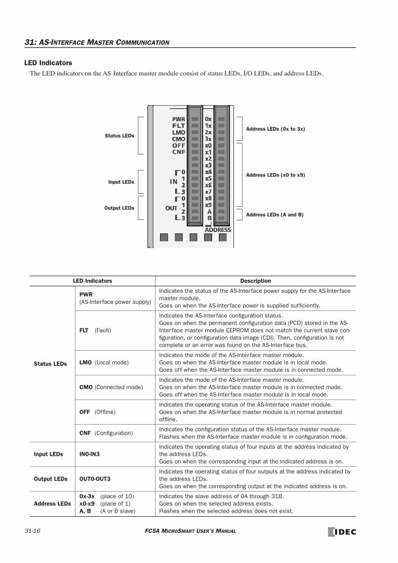
31: AS-INTERFACE MASTER COMMUNICATION
LED IndicatorsThe LED indicators on the AS-Interface master module consist of status LEDs, I/O LEDs, and address LEDs.
LED Indicators Description
Status LEDs
PWR (AS-Interface power supply)
Indicates the status of the AS-Interface power supply for the AS-Interface master module.Goes on when the AS-Interface power is supplied sufficiently.
FLT (Fault)
Indicates the AS-Interface configuration status. Goes on when the permanent configuration data (PCD) stored in the AS-Interface master module EEPROM does not match the current slave con-figuration, or configuration data image (CDI). Then, configuration is not complete or an error was found on the AS-Interface bus.
LMO (Local mode)Indicates the mode of the AS-Interface master module.Goes on when the AS-Interface master module is in local mode.Goes off when the AS-Interface master module is in connected mode.
CMO (Connected mode)Indicates the mode of the AS-Interface master module.Goes on when the AS-Interface master module is in connected mode.Goes off when the AS-Interface master module is in local mode.
OFF (Offline)Indicates the operating status of the AS-Interface master module.Goes on when the AS-Interface master module is in normal protected offline.
CNF (Configuration)Indicates the configuration status of the AS-Interface master module.Flashes when the AS-Interface master module is in configuration mode.
Input LEDs IN0-IN3Indicates the operating status of four inputs at the address indicated by the address LEDs.Goes on when the corresponding input at the indicated address is on.
Output LEDs OUT0-OUT3Indicates the operating status of four outputs at the address indicated by the address LEDs.Goes on when the corresponding output at the indicated address is on.
Address LEDs0x-3x (place of 10) x0-x9 (place of 1) A, B (A or B slave)
Indicates the slave address of 0A through 31B.Goes on when the selected address exists.Flashes when the selected address does not exist.
Status LEDs
Input LEDs
Output LEDs
Address LEDs (x0 to x9)
Address LEDs (0x to 3x)
Address LEDs (A and B)
31-16 FC5A MICROSMART USER’S MANUAL

31: AS-INTERFACE MASTER COMMUNICATION
Status LEDsThe operation modes of the AS-Interface master module can be changed by pressing the pushbuttons on the front of the AS-Interface master module or by executing ASI commands. The operation modes can be confirmed on the six status LEDs on the AS-Interface master module. For details about the ASI commands, see page 31-30.
Status LED Indication
*1: Goes off when AS-Interface power is not supplied. *2: Goes on when an error is found on the AS-Interface bus.
Address LEDs and I/O LEDsThe operating status and I/O status of each slave can be monitored on the address LEDs and I/O LEDs on the front of the AS-Interface master module.
Slave Operating StatusThe operating status of each slave can be determined by viewing the address LEDs and I/O LEDs.
Slave I/O StatusThe I/O status of each slave can be monitored on the address LEDs and I/O LEDs. Use the short press to change the slave address when monitoring slave I/O status on the AS-Interface master module. A short press on PB1 increments the address. At the last address (31B), another short press will return to the first address (0A). A short press on PB2 decre-ments the address. At the first address (0A), another short press will return to the last address (31B).
The figures below illustrate what happens when you press the PB1 button while the address LEDs indicate 25A. The address LEDs increment to 26A where a slave is assigned. Note that the address LEDs flash if no slave is assigned.
Status LED PWR FLT LMO CMO OFF CNF
Connected Mode
Normal Protected Mode ON *1 OFF *2 OFF ON OFF OFF
Normal Protected Offline ON *1 ON OFF ON ON OFF
Normal Protected Data Exchange Off
ON *1 ON OFF ON OFF OFF
Local ModeProtected Mode ON *1 OFF *2 ON OFF OFF OFF
Configuration Mode ON *1 OFF *2 ON OFF OFF Flash
Address LED I/O LED Description
ON ON or OFF The slave at this address is active.
ON Flash The slave at this address is active, but has an error.
Flash OFF This address is not assigned a slave.
OFF OFFThe AS-Interface bus communication is disabled because the AS-Interface power is not supplied or the AS-Interface master module is in normal protected offline.
Monitoring Slave Address 25A Address LEDs are flashing since no slave is assigned.
Short press on PB1
I/O LEDs indicate statuses
Monitoring Slave Address 26AAddress LEDs go on and I/O LEDs indicate the statuses.
FC5A MICROSMART USER’S MANUAL 31-17

31: AS-INTERFACE MASTER COMMUNICATION
AS-Interface OperandsThis section describes AS-Interface operands assigned in the CPU module to control and monitor the AS-Interface master module, and describes ASI commands used to update AS-Interface operands in the CPU module or to control the AS-Inter-face master module.
The FC5A MicroSmart CPU modules can be used with one or two AS-Interface master modules. For the first AS-Interface master module, which is mounted closer to the CPU module, the AS-Interface objects can be accessed through the AS-Interface operands, such as internal relays M1300 through M1997 and data registers D1700 through D1999 as shown on page 31-19.
Details about AS-Interface objects for AS-Interface master module 2 are described on the following pages.
Processing TimeFor AS-Interface master module 1, AS-Interface internal relays for digital I/O and status information, and data registers for LAS, LDS, LPF are updated in every scan. Data registers for analog I/O operands are also updated in every scan only when analog I/O are connected to the AS-Interface bus. The processing times for these AS-Interface operands are shown in the table on page 31-19.
Other AS-Interface data registers are updated when an ASI command is executed in the CPU module. For the processing times of the ASI commands, see page 31-30.
For AS-Interface master module 1, AS-Interface objects are updated using the RUNA instruction.
AS-Interface Master Module 1 AS-Interface Master Module 2AS-Interface Power Supply ×××× 2
To two separate AS-Interface networks
Note: When using two AS-Interface master modules, two AS-Interface power supplies are needed. Since the AS-Interface cable transmits both signals and power, each network requires a separate power supply.
LadderProcessing
OtherProcessing
AS-InterfaceProcessing
Constantly Updated OperandsM1300-M1997
ASI CommandD1941-D1945
ASI Command
AS-Interface
AS-Interface Objects
IDI, ODI Status InformationAnalog I/OLAS, LDS, LPF
LPS, CDI, PCD PI, PP Slave 0 ID1D1776-D1940
Updated Operands
D1700-D1775
AS-Interface Operands
Master Module 1
MicroSmart CPU Module
AS-Interface Master Module 2
AS-Interface Objects
IDI, ODI Status InformationAnalog I/OLAS, LDS, LPF
RUNA Instruction
31-18 FC5A MICROSMART USER’S MANUAL

31: AS-INTERFACE MASTER COMMUNICATION
Accessing AS-Interface Objects for AS-Interface Master Module 1The I/O data and parameters of slaves on the AS-Interface bus, the status of the AS-Interface bus, and various list informa-tion of the slaves are allocated to the AS-Interface master module EEPROM. This information is called AS-Interface objects, which can be accessed through the AS-Interface operands, such as internal relays M1300 through M1997 and data registers D1700 through D1999. The allocation for AS-Interface master module 1 is shown in the table below.
*1: The time required for the CPU module to update the operand data. When using AS-Interface master module 1, the scan time increases by a minimum of 10 ms. For AS-Interface master module 2, see page 31-32.
*2: These AS-Interface operand data can be read or written using WindLDR. For details, see page 31-34.*3: The LPS, PCD, and PP are set and downloaded to the CPU module using WindLDR. For details, see page 31-36.*4: The analog I/O data is updated only when an analog slave is connected to the AS-Interface bus.
Accessing AS-Interface Objects for AS-Interface Master Module 2When using two AS-Interface master modules, the AS-Interface objects for the second AS-Interface master module can be assigned to any internal relays and data registers and accessed using RUNA or STPA instructions. See page 31-32.
MicroSmart CPU Module Allocation No. Precessing
Time (ms) *1Read/Write
AS-Interface Master Module EEPROMOperand Updated
OperandAS-Interface
Master Module 1AS-Interface Object
AS-Interface Internal Relays
M1300-M1617 3.0 R *2 Digital input (IDI: input data image)
Every scan
M1620-M1937 3.0 W *2 Digital output (ODI: output data image)
M1940-M1997 1.0 R Status information
AS-Interface Data Registers
D1700-D1731 5.2 R Analog input *4
D1732-D1763 5.2 W Analog output *4
D1764-D1767 1.0 R *2 List of active slaves (LAS)
D1768-D1771 1.0 R *2 List of detected slaves (LDS)
D1772-D1775 1.0 R *2 List of peripheral fault slaves (LPF)
D1776-D1779 1.0 R/W *2*3 List of projected slaves (LPS)
Each time ASI command is executed
D1780-D1811 5.2 R *2 Configuration data image A (CDI)
D1812-D1843 5.2 R *2 Configuration data image B (CDI)
D1844-D1875 5.2 R/W *2*3 Permanent configuration data A (PCD)
D1876-D1907 5.2 R/W *2*3 Permanent configuration data B (PCD)
D1908-D1923 3.0 R *2 Parameter image (PI)
D1924-D1939 3.0 R/W *2*3 Permanent parameter (PP)
D1940 0.7 R/W Slave 0 ID1 code
D1941-D1945 — R/W ASI command description —
D1946-D1999 — — (reserved) —
FC5A MICROSMART USER’S MANUAL 31-19

31: AS-INTERFACE MASTER COMMUNICATION
I/O Data for AS-Interface Master ModuleThe AS-Interface master module can process digital I/O data and analog I/O data. Digital I/O data can be a maximum of 4 digital inputs and 4 digital outputs per slave. Analog I/O data consists of 4 channels of 16-bit analog input or output data per slave.
Digital I/O Data of Standard Slaves and Expansion SlavesFor AS-Interface master module 1, the digital I/O data for standard slaves and A/B slaves (sensors and actuators) on the AS-Interface bus are allocated to the AS-Interface internal relays in the ascending order starting with slave 0. The input data image (IDI) for each slave is allocated to M1300 through M1617, and the output data image (ODI) is allocated to M1620 through M1937. For example, in the case of slave 3A, the input data is allocated to M1314 (DI0) through M1317 (DI3), and the output data is allocated to M1634 (DO0) through M1637 (DO3).
For AS-Interface master module 2, the digital I/O data can be accessed using RUNA or STPA instruction.
• Digital Input Data Image (IDI)
* Data Address represents the offset from the Data Address designated in the RUNA or STPA instruction dialog box.
AS-Interface Master Module 1
Allocation No.
AS-Interface Master Module 2Data Address *
Data Format
7(DI3)
6(DI2)
5(DI1)
4(DI0)
3(DI3)
2(DI2)
1(DI1)
0(DI0)
M1300 +0 (low byte) Slave 1(A) (Slave 0)
M1310 +0 (high byte) Slave 3(A) Slave 2(A)
M1320 +1 (low byte) Slave 5(A) Slave 4(A)
M1330 +1 (high byte) Slave 7(A) Slave 6(A)
M1340 +2 (low byte) Slave 9(A) Slave 8(A)
M1350 +2 (high byte) Slave 11(A) Slave 10(A)
M1360 +3 (low byte) Slave 13(A) Slave 12(A)
M1370 +3 (high byte) Slave 15(A) Slave 14(A)
M1380 +4 (low byte) Slave 17(A) Slave 16(A)
M1390 +4 (high byte) Slave 19(A) Slave 18(A)
M1400 +5 (low byte) Slave 21(A) Slave 20(A)
M1410 +5 (high byte) Slave 23(A) Slave 22(A)
M1420 +6 (low byte) Slave 25(A) Slave 24(A)
M1430 +6 (high byte) Slave 27(A) Slave 26(A)
M1440 +7 (low byte) Slave 29(A) Slave 28(A)
M1450 +7 (high byte) Slave 31(A) Slave 30(A)
M1460 +8 (low byte) Slave 1B —
M1470 +8 (high byte) Slave 3B Slave 2B
M1480 +9 (low byte) Slave 5B Slave 4B
M1490 +9 (high byte) Slave 7B Slave 6B
M1500 +10 (low byte) Slave 9B Slave 8B
M1510 +10 (high byte) Slave 11B Slave 10B
M1520 +11 (low byte) Slave 13B Slave 12B
M1530 +11 (high byte) Slave 15B Slave 14B
M1540 +12 (low byte) Slave 17B Slave 16B
M1550 +12 (high byte) Slave 19B Slave 18B
M1560 +13 (low byte) Slave 21B Slave 20B
M1570 +13 (high byte) Slave 23B Slave 22B
M1580 +14 (low byte) Slave 25B Slave 24B
M1590 +14 (high byte) Slave 27B Slave 26B
M1600 +15 (low byte) Slave 29B Slave 28B
M1610 +15 (high byte) Slave 31B Slave 30B
31-20 FC5A MICROSMART USER’S MANUAL

31: AS-INTERFACE MASTER COMMUNICATION
• Digital Output Data Image (ODI)
* Data Address represents the offset from the Data Address designated in the RUNA or STPA instruction dialog box.
AS-Interface Master Module 1
Allocation No.
AS-Interface Master Module 2Data Address *
Data Format
7(DO3)
6(DO2)
5(DO1)
4(DO0)
3(DO3)
2(DO2)
1(DO1)
0(DO0)
M1620 +0 (low byte) Slave 1(A) (Slave 0)
M1630 +0 (high byte) Slave 3(A) Slave 2(A)
M1640 +1 (low byte) Slave 5(A) Slave 4(A)
M1650 +1 (high byte) Slave 7(A) Slave 6(A)
M1660 +2 (low byte) Slave 9(A) Slave 8(A)
M1670 +2 (high byte) Slave 11(A) Slave 10(A)
M1680 +3 (low byte) Slave 13(A) Slave 12(A)
M1690 +3 (high byte) Slave 15(A) Slave 14(A)
M1700 +4 (low byte) Slave 17(A) Slave 16(A)
M1710 +4 (high byte) Slave 19(A) Slave 18(A)
M1720 +5 (low byte) Slave 21(A) Slave 20(A)
M1730 +5 (high byte) Slave 23(A) Slave 22(A)
M1740 +6 (low byte) Slave 25(A) Slave 24(A)
M1750 +6 (high byte) Slave 27(A) Slave 26(A)
M1760 +7 (low byte) Slave 29(A) Slave 28(A)
M1770 +7 (high byte) Slave 31(A) Slave 30(A)
M1780 +8 (low byte) Slave 1B —
M1790 +8 (high byte) Slave 3B Slave 2B
M1800 +9 (low byte) Slave 5B Slave 4B
M1810 +9 (high byte) Slave 7B Slave 6B
M1820 +10 (low byte) Slave 9B Slave 8B
M1830 +10 (high byte) Slave 11B Slave 10B
M1840 +11 (low byte) Slave 13B Slave 12B
M1850 +11 (high byte) Slave 15B Slave 14B
M1860 +12 (low byte) Slave 17B Slave 16B
M1870 +12 (high byte) Slave 19B Slave 18B
M1880 +13 (low byte) Slave 21B Slave 20B
M1890 +13 (high byte) Slave 23B Slave 22B
M1900 +14 (low byte) Slave 25B Slave 24B
M1910 +14 (high byte) Slave 27B Slave 26B
M1920 +15 (low byte) Slave 29B Slave 28B
M1930 +15 (high byte) Slave 31B Slave 30B
• Immediately after power up, the digital I/O data of standard slaves and expansion slaves cannot be accessed. Data communication between the CPU module and the connected slaves starts when spe-cial internal relay M1945 (Normal_Operation_Active) turns on. Make sure that M1945 is on before starting to access the slave I/O data.
Caution
FC5A MICROSMART USER’S MANUAL 31-21

31: AS-INTERFACE MASTER COMMUNICATION
Analog I/O Data of Analog SlavesFor AS-Interface master module 1, the I/O data for a maximum of seven analog slaves (four channels for each slave) on the AS-Interface bus is stored to AS-Interface data registers in the CPU module. The analog slave addresses (1 to 31) are in the ascending order. The input data for each analog slave is allocated to data registers D1700 to D1731, and the output data is allocated to D1732 to D1763.
For AS-Interface master module 2, the analog I/O data can be accessed using RUNA or STPA instructions.
The AS-Interface master module is compliant with analog slave profile 7.3.
• Analog Input Data
• The maximum number of analog slaves that can be connected to the AS-Interface bus is seven. Do not connect eight or more analog slaves to one bus, otherwise the slaves will not function correctly.
• When data registers D1700 through D1731 allocated to analog inputs contain 7FFF, do not use this data for programming, because this value is reserved for a special meaning as follows:
Unused channel on a slave allocated to analog slave. (For a channel on a slave not allocated an analog slave, the corresponding data register holds an indefinite value.) Data overflow. Communication between the master and analog slave is out of synchronism.
• When using analog slaves, read the user’s manual for the analog slave to process the data properly.
AS-Interface Master Module 1 Allocation No.
AS-Interface Master Module 2Data Address *
Channel No. Data Format
D1700 +0 Channel 1
1st data(AI0)
D1701 +1 Channel 2D1702 +2 Channel 3D1703 +3 Channel 4D1704 +4 Channel 1
2nd data(AI1)
D1705 +5 Channel 2D1706 +6 Channel 3D1707 +7 Channel 4D1708 +8 Channel 1
3rd data(AI2)
D1709 +9 Channel 2D1710 +10 Channel 3D1711 +11 Channel 4D1712 +12 Channel 1
4th data(AI3)
D1713 +13 Channel 2D1714 +14 Channel 3D1715 +15 Channel 4D1716 +16 Channel 1
5th data(AI4)
D1717 +17 Channel 2D1718 +18 Channel 3D1719 +19 Channel 4D1720 +20 Channel 1
6th data(AI5)
D1721 +21 Channel 2D1722 +22 Channel 3D1723 +23 Channel 4D1724 +24 Channel 1
7th data(AI6)
D1725 +25 Channel 2D1726 +26 Channel 3D1727 +27 Channel 4D1728 +28 —
(reserved)D1729 +29 —D1730 +30 —D1731 +31 —
Caution
31-22 FC5A MICROSMART USER’S MANUAL

31: AS-INTERFACE MASTER COMMUNICATION
• Analog Output Data
* Data Address represents the offset from the Data Address designated in the RUNA or STPA instruction dialog box.
For example, when analog input slaves 1, 13 and 20, analog output slaves 5 and 25, and analog I/O slaves 14 and 21 are used, the analog I/O slave data will be allocated by configuration as shown below and maintained until the next configura-tion is executed. Four channels (8 bytes) are always reserved for each slave.
The data range area for AS-Interface module 2 is the same.
AS-Interface Master Module 1 Allocation No.
AS-Interface Master Module 2Data Address *
Channel No. Data Format
D1732 +0 Channel 1
1st data(AO0)
D1733 +1 Channel 2D1734 +2 Channel 3D1735 +3 Channel 4D1736 +4 Channel 1
2nd data(AO1)
D1737 +5 Channel 2D1738 +6 Channel 3D1739 +7 Channel 4D1740 +8 Channel 1
3rd data(AO2)
D1741 +9 Channel 2D1742 +10 Channel 3D1743 +11 Channel 4D1744 +12 Channel 1
4th data(AO3)
D1745 +13 Channel 2D1746 +14 Channel 3D1747 +15 Channel 4D1748 +16 Channel 1
5th data(AO4)
D1749 +17 Channel 2D1750 +18 Channel 3D1751 +19 Channel 4D1752 +20 Channel 1
6th data(AO5)
D1753 +21 Channel 2D1754 +22 Channel 3D1755 +23 Channel 4D1756 +24 Channel 1
7th data(AO6)
D1757 +25 Channel 2D1758 +26 Channel 3D1759 +27 Channel 4D1760 +28 —
(reserved)D1761 +29 —D1762 +30 —D1763 +31 —
Analog Slave ModuleAS-Interface Master
Module 1 Data Storage
Analog Input SlaveAS-Interface Master
Module 1 Data Storage
Analog Output Slave
1st D1700-D1703 Slave 1 D1732-D1735 Unused2nd D1704-D1707 Unused D1736-D1739 Slave 53rd D1708-D1711 Slave 13 D1740-D1743 Unused4th D1712-D1715 Slave 14 D1744-D1747 Slave 145th D1716-D1719 Slave 20 D1748-D1751 Unused6th D1720-D1723 Slave 21 D1752-D1755 Slave 217th D1724-D1727 Unused D1756-D1759 Slave 25
(8th) (D1728-D1731) (reserved) (D1760-D1763) (reserved)
FC5A MICROSMART USER’S MANUAL 31-23
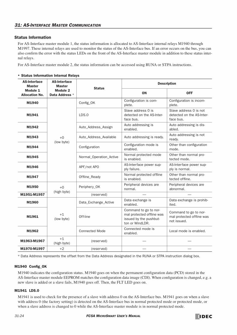
31: AS-INTERFACE MASTER COMMUNICATION
Status InformationFor AS-Interface master module 1, the status information is allocated to AS-Interface internal relays M1940 through M1997. These internal relays are used to monitor the status of the AS-Interface bus. If an error occurs on the bus, you can also confirm the error with the status LEDs on the front of the AS-Interface master module in addition to these status inter-nal relays.
For AS-Interface master module 2, the status information can be accessed using RUNA or STPA instructions.
• Status Information Internal Relays
* Data Address represents the offset from the Data Address designated in the RUNA or STPA instruction dialog box.
M1940 Config_OK
M1940 indicates the configuration status. M1940 goes on when the permanent configuration data (PCD) stored in the AS-Interface master module EEPROM matches the configuration data image (CDI). When configuration is changed, e.g. a new slave is added or a slave fails, M1940 goes off. Then, the FLT LED goes on.
M1941 LDS.0
M1941 is used to check for the presence of a slave with address 0 on the AS-Interface bus. M1941 goes on when a slave with address 0 (the factory setting) is detected on the AS-Interface bus in normal protected mode or protected mode, or when a slave address is changed to 0 while the AS-Interface master module is in normal protected mode.
AS-Interface Master
Module 1 Allocation No.
AS-Interface Master
Module 2Data Address *
StatusDescription
ON OFF
M1940
+0(low byte)
Config_OKConfiguration is com-plete.
Configuration is incom-plete.
M1941 LDS.0Slave address 0 is detected on the AS-Inter-face bus.
Slave address 0 is not detected on the AS-Inter-face bus.
M1942 Auto_Address_AssignAuto addressing is enabled.
Auto addressing is dis-abled.
M1943 Auto_Address_Available Auto addressing is ready.Auto addressing is not ready.
M1944 ConfigurationConfiguration mode is enabled.
Other than configuration mode.
M1945 Normal_Operation_ActiveNormal protected mode is enabled.
Other than normal pro-tected mode.
M1946 APF/not APOAS-Interface power sup-ply failure.
AS-Interface power sup-ply is normal.
M1947 Offline_ReadyNormal protected offline is enabled.
Other than normal pro-tected offline.
M1950 +0(high byte)
Periphery_OKPeripheral devices are normal.
Peripheral devices are abnormal.
M1951-M1957 (reserved) — —
M1960
+1(low byte)
Data_Exchange_ActiveData exchange is enabled.
Data exchange is prohib-ited.
M1961 Off-line
Command to go to nor-mal protected offline was issued by the pushbut-ton or WindLDR.
Command to go to nor-mal protected offline was not issued.
M1962 Connected ModeConnected mode is enabled.
Local mode is enabled.
M1963-M1967+1
(high byte)(reserved) — —
M1970-M1997 +2 (reserved) — —
31-24 FC5A MICROSMART USER’S MANUAL

31: AS-INTERFACE MASTER COMMUNICATION
M1942 Auto_Address_Assign
M1942 indicates that the auto addressing function is enabled. The default setting is “enabled,” and M1942 is normally on. This setting can be changed using the ASI commands Enable Auto Addressing and Disable Auto Addressing.
Note: When the auto addressing function is enabled at the AS-Interface master module and a slave fails, you can replace the slave with a new slave which has the same identification codes without stopping the AS-Interface bus.
• If the replacement slave is assigned the same address and has the same identification codes as the failed slave, the replacement slave is automatically added to the LDS (list of detected slaves) to continue operation. If the assigned address or the identification codes of the replacement slave are different from the failed slave, the FLT LED will go on.
• When replacing a failed slave with a new slave which is assigned address 0 (factory setting) and has the same identifica-tion codes, the new slave will be assigned the address of the failed slave and added to the LDS and LAS (list of active slaves). If the identification codes of the replacement slave are different from the failed slave, the FLT LED will go on.
• The auto addressing function for a replacement slave works only when one slave has failed. This function cannot be used to replace multiple slaves.
M1943 Auto_Address_Available
M1943 indicates whether or not the conditions for the auto addressing function are satisfied. M1943 goes on when the auto addressing function is enabled and there is one faulty slave (a slave which cannot be recognized by the AS-Interface mas-ter module) on the AS-Interface bus.
M1944 Configuration
M1944 indicates whether the AS-Interface master module is in configuration mode (on) or other mode (off). While config-uration mode is enabled, M1944 remains on, and the CNF LED flashes.
M1945 Normal_Operation_Active
M1945 remains on while the AS-Interface master module is in normal protected mode. M1945 is off while in other modes. When M1945 turns on, the CPU module starts to exchange data communication with the connected slaves.
M1946 APF/not APO
M1946 goes on when the AS-Interface power supply has failed, then the PWR LED goes off.
M1947 Offline_Ready
M1947 indicates that the AS-Interface master module is in normal protected offline. While in normal protected offline, M1947 remains on and the OFF LED also remains on.
M1950 Periphery_OK
M1950 remains on while the AS-Interface master module does not detect a failure in peripheral devices. When a failure is found, M1950 goes off.
M1960 Data_Exchange_Active
M1960 indicates that data exchange is enabled. While M1960 is on, the AS-Interface master module is in normal protected mode, and data exchange between the AS-Interface master module and slaves is enabled. The data exchange can be enabled and disabled using the ASI commands Enable Data Exchange and Prohibit Data Exchange.
M1961 Off-line
M1961 goes on when a command to switch to normal protected offline is issued. To switch to normal protected offline from normal protected mode, either press the PB2 button on the AS-Interface master module or issue the ASI command Go to Normal Protected Offline. M1961 remains on until normal protected offline is exited.
M1962 Connected Mode
M1962 indicates that the AS-Interface master module is in connected mode. While in connected mode, M1962 remains on. Then, LMO LED remains off and the CMO LED remains on.
FC5A MICROSMART USER’S MANUAL 31-25

31: AS-INTERFACE MASTER COMMUNICATION
Slave List InformationFor AS-Interface master module 1, data registers D1764 through D1779 are assigned to slave list information to determine the operating status of the slaves. The slave list information is grouped into four lists. List of active slaves (LAS) shows the slaves currently in operation. List of detected slaves (LDS) the slaves detected on the AS-Interface bus. List of peripheral fault slaves (LPF) the faulty slaves. List of projected slaves (LPS) the slave configuration stored in the AS-Interface master module.
For AS-Interface master module 2, the slave list information can be accessed using RUNA or STPA instructions.
List of Active Slaves (LAS)
For AS-Interface master module 1, data registers D1764 through D1767 are allocated to read the LAS. You can check the register bits to determine the operating status of each slave. When a bit is on, it indicates that the corresponding slave is active.
List of Detected Slaves (LDS)
For AS-Interface master module 1, data registers D1768 through D1771 are allocated to read the LDS. You can check the register bits to determine the detection status of each slave. When a bit is on, it indicates that the corresponding slave has been detected by the master.
List of Peripheral Fault Slaves (LPF)
For AS-Interface master module 1, data registers D1772 through D1775 are allocated to read the LPF. You can check the register bits to determine the fault status of each slave. When a bit is on, it indicates that the corresponding slave is faulty.
* Data Address represents the offset from the Data Address designated in the RUNA or STPA instruction dialog box.
AS-Interface Master Module 1 Allocation No.
AS-Interface Master Module 2Data Address *
Data FormatBits 15 to 8 Bits 7 to 0
D1764 +0 Slaves 15(A) to 8(A) Slaves 7(A) to 0D1765 +1 Slaves 31(A) to 24(A) Slaves 23(A) to 16(A)D1766 +2 Slaves 15B to 8B Slaves 7B to (0B)D1767 +3 Slaves 31B to 24B Slaves 23B to 16B
AS-Interface Master Module 1 Allocation No.
AS-Interface Master Module 2Data Address *
Data FormatBits 15 to 8 Bits 7 to 0
D1768 +4 Slaves 15(A) to 8(A) Slaves 7(A) to 0D1769 +5 Slaves 31(A) to 24(A) Slaves 23(A) to 16(A)D1770 +6 Slaves 15B to 8B Slaves 7B to (0B)D1771 +7 Slaves 31B to 24B Slaves 23B to 16B
AS-Interface Master Module 1 Allocation No.
AS-Interface Master Module 2Data Address *
Data FormatBits 15 to 8 Bits 7 to 0
D1772 +8 Slaves 15(A) to 8(A) Slaves 7(A) to 0D1773 +9 Slaves 31(A) to 24(A) Slaves 23(A) to 16(A)D1774 +10 Slaves 15B to 8B Slaves 7B to (0B)D1775 +11 Slaves 31B to 24B Slaves 23B to 16B
31-26 FC5A MICROSMART USER’S MANUAL

31: AS-INTERFACE MASTER COMMUNICATION
List of Projected Slaves (LPS)
For AS-Interface master module 1, D1776 through D1779 are allocated to read and write the LPS. The LPS settings are stored to the AS-Interface master module when either Auto Configuration or Manual Configuration is executed on WindLDR. The ASI command Read LPS can be used to read the LPS data to data registers D1776 through D1779. Then, you can check the register bits to determine the slave projection. When a bit is on, it indicates that the corresponding slave is set as a projected slave. After changing the LPS settings, execute the ASI command Read LPS, then you can use the updated data for program execution.
For AS-Interface master module 2, the list of projected slaves cannot be accessed using the RUNA or STPA instruction.
Slave Identification Information (Slave Profile)For AS-Interface master module 1, data registers D1780 through D1940 are assigned to the slave identification informa-tion, or the slave profile. The slave profile includes configuration data and parameters to indicate the slave type and slave operation, respectively.
For AS-Interface master module 2, the slave identification information can not be accessed using RUNA or STPA instruc-tions.
Configuration Data Image (CDI)
For AS-Interface master module 1, data registers D1780 through D1843 are allocated to read the CDI of each slave. The CDI is the current slave configuration data collected by the AS-Interface master module at power-up and stored in the AS-Interface master module.
The CDI is made up of four codes: the ID code, I/O code, ID2 code, and ID1 code. The CDI of slaves not connected to the AS-Interface bus is FFFFh.
The ASI command Read CDI can be used to read the CDI data to data registers D1780 through D1843. Execute the ASI command Read CDI before using the CDI data for program execution.
AS-Interface Master Module 1 Allocation No.
AS-Interface Master Module 2Data Address
Data FormatBits 15 to 8 Bits 7 to 0
D1776 — Slaves 15(A) to 8(A) Slaves 7(A) to 0D1777 — Slaves 31(A) to 24(A) Slaves 23(A) to 16(A)D1778 — Slaves 15B to 8B Slaves 7B to (0B)D1779 — Slaves 31B to 24B Slaves 23B to 16B
AS-Interface Master Module 1
Allocation No.
AS-Interface Master Module 2
Data Address
Data FormatBits 15 to 12
ID CodeBits 11 to 8
I/O CodeBits 7 to 4ID2 Code
Bits 3 to 0ID1 Code
D1780 — Slave 0D1781 — Slave 1(A)D1782 — Slave 2(A)
D(1780+N) — Slave N(A)D1811 — Slave 31(A)D1812 — (unused)D1813 — Slave 1B
D(1812+N) — Slave NBD1843 — Slave 31B
FC5A MICROSMART USER’S MANUAL 31-27

31: AS-INTERFACE MASTER COMMUNICATION
Permanent Configuration Data (PCD)
For AS-Interface master module 1, data registers D1844 through D1907 are allocated to read and write the PCD of each slave. Like the CDI, the PCD is made up of four codes: the ID code, I/O code, ID2 code, and ID1 code.
When auto configuration is executed, the CDI is copied to the PCD and stored in the EEPROM of the AS-Interface master module. When you execute manual configuration, you can set the PCD using the Configure Slave dialog box on WindLDR. Set the PCD of each slave to the same value as its CDI. If the PCD is different from the CDI for a slave, then that slave does not function correctly. Set FFFFh to the PCD of vacant slave numbers.
The ASI command Read PCD can be used to read the PCD data to data registers D1844 through D1907. Execute the ASI command Read PCD before using the PCD data for program execution.
Parameter Image (PI)
For AS-Interface master module 1, data registers D1908 through D1923 are allocated to read the PI of each slave. The PI is made up of four parameters: the P3, P2, P1, and P0. The PI is the current slave parameter data collected by the AS-Inter-face master module at power-up and stored in the AS-Interface master module. To change the PI settings, use WindLDR (Slave Status dialog box) or execute the ASI command Change Slave PI.
The ASI command Read PI can be used to read PI data to data registers D1908 through D1923. After changing the PI set-tings, execute the ASI command Read PI, then you can use the updated PI data for program execution.
AS-Interface Master Module 1
Allocation No.
AS-Interface Master Module 2
Data Address
Data FormatBits 15 to 12
ID CodeBits 11 to 8
I/O CodeBits 7 to 4ID2 Code
Bits 3 to 0ID1 Code
D1844 — Slave 0D1845 — Slave 1(A)D1846 — Slave 2(A)
D(1844+N) — Slave N(A)D1875 — Slave 31(A)D1876 — (unused)D1877 — Slave 1B
D(1876+N) — Slave NBD1907 — Slave 31B
AS-Interface Master Module 1
Allocation No.
AS-Interface Master Module 2
Data Address
Data FormatBits 15 to 12P3/P2/P1/P0
Bits 11 to 8P3/P2/P1/P0
Bits 7 to 4P3/P2/P1/P0
Bits 3 to 0P3/P2/P1/P0
D1908 — Slave 3(A) Slave 2(A) Slave 1(A) Slave 0D1909 — Slave 7(A) Slave 6(A) Slave 5(A) Slave 4(A)D1910 — Slave 11(A) Slave 10(A) Slave 9(A) Slave 8(A)
D(1908+N/4) — Slave (N+3)(A) Slave (N+2)(A) Slave (N+1)(A) Slave N(A)D1915 — Slave 31(A) Slave 30(A) Slave 29(A) Slave 28(A)D1916 — Slave 3B Slave 2B Slave 1B (unused)D1917 — Slave 7B Slave 6B Slave 5B Slave 4B
D(1916+N/4) — Slave (N+3)B Slave (N+2)B Slave (N+1)B Slave NBD1923 — Slave 31B Slave 30B Slave 29B Slave 28B
31-28 FC5A MICROSMART USER’S MANUAL

31: AS-INTERFACE MASTER COMMUNICATION
Permanent Parameter (PP)
For AS-Interface master module 1, data registers D1924 through D1939 are allocated to read and write the PP of each slave. Like the PI, the PP is made up of four parameters: the P3, P2, P1, and P0. When auto configuration is executed, the PI is copied to the PP and stored in the EEPROM of the AS-Interface master module. When you execute manual configu-ration, you can set the PP using the Configure Slave dialog box on WindLDR.
The ASI command Read PP can be used to read PP data to data registers D1924 through D1939. After changing the PP set-tings, execute the ASI command Read PP, then you can use the updated PP data for program execution.
Changing ID1 Code of Slave 0
For AS-Interface master module 1, data register D1940 is allocated to read and write the ID1 code of slave 0. To change the slave 0 ID1 settings, store a required value in D1940 and execute the ASI command Write Slave 0 ID1. The ASI com-mand Read Slave 0 ID1 can be used to read slave 0 ID1 data to data register D1940. After changing the slave 0 ID1 set-tings, execute the ASI command Read Slave 0 ID1, then you can use the updated slave 0 ID1 data for program execution.
AS-Interface Master Module 1
Allocation No.
AS-Interface Master Module 2
Data Address
Data FormatBits 15 to 12P3/P2/P1/P0
Bits 11 to 8P3/P2/P1/P0
Bits 7 to 4P3/P2/P1/P0
Bits 3 to 0P3/P2/P1/P0
D1924 — Slave 3(A) Slave 2(A) Slave 1(A) Slave 0D1925 — Slave 7(A) Slave 6(A) Slave 5(A) Slave 4(A)D1926 — Slave 11(A) Slave 10(A) Slave 9(A) Slave 8(A)
D(1924+N/4) — Slave (N+3)(A) Slave (N+2)(A) Slave (N+1)(A) Slave N(A)D1931 — Slave 31(A) Slave 30(A) Slave 29(A) Slave 28(A)D1932 — Slave 3B Slave 2B Slave 1B (unused)D1933 — Slave 7B Slave 6B Slave 5B Slave 4B
D(1932+N/4) — Slave (N+3)B Slave (N+2)B Slave (N+1)B Slave NBD1939 — Slave 31B Slave 30B Slave 29B Slave 28B
AS-Interface Master Module 1
Allocation No.
AS-Interface Master Module 2
Data Address
Data Format
Bits 15 to 12 Bits 11 to 8 Bits 7 to 4 Bits 3 to 0
D1940 — — — — ID1 code
FC5A MICROSMART USER’S MANUAL 31-29

31: AS-INTERFACE MASTER COMMUNICATION
ASI Commands (AS-Interface Master Module 1)The ASI commands are used to update AS-Interface operands in the CPU module or to control the AS-Interface master module 1. Data registers D1941 through D1944 are used to store command data. D1945 is used to store a request code before executing the command. While the command is executed, D1945 stores status and result codes.
ASI Command Format
ASI Command DataTo execute an ASI command, store required values to data resisters D1941 through D1945 as listed in the table below:
*1: WindLDR has the Slave Status dialog box to execute this command to write a PI value to a designated slave. See Sam-ple Program on page 31-31.
*2: WindLDR has the Change Slave Address dialog box to execute this command.
*3: Completed in a scan when the five data registers store respective values. When completed, D1945 stores 4. See Request and Result Codes on page 31-31. Other commands takes several scans to complete execution.
*4: Each scan time extends by 0.8 ms. At least 1 sec is required until the ASI command takes effect.
Note: Specify the slave address in the data register as shown in the table below:
Command Part (8 bytes) Request/Result
D1941 D1942 D1943 D1944 D1945
ASI CommandProcessing Time (ms)
DescriptionCommand Data (Hexadecimal)
D1941 D1942 D1943 D1944 D1945
Read LPS 1.0 *3 Reads LPS to D1776-D1779 010B 084C 0000 0000 0001
Read CDI 10.4 *3 Reads CDI to D1780-D1843 010C 4050 0000 0000 0001
Read PCD 10.4 *3 Reads PCD to D1844-D1907 010E 4090 0000 0000 0001
Read PI 3.0 *3 Reads PI to D1908-D1923 0107 20D0 0000 0000 0001
Read PP 3.0 *3 Reads PP to D1924-D1939 0108 20E0 0000 0000 0001
Read Slave 0 ID1 0.7 *3 Reads slave 0 ID1 to D1940 0109 02F0 0000 0000 0001
Write Slave 0 ID1 0.7 *3 Writes D1940 to slave 0 ID1 0209 02F0 0000 0000 0001
Copy PI to PP 0.8 *4 Copies parameter image to perma-nent parameter
0306 0100 0000 0000 0001
Change Slave PI *1 0.8 *4 Writes PI (∗) to slave (∗∗) (Note) 0306 0102 000∗ 00∗∗ 0001
Go to Normal Protected Offline 0.8 *4 From normal protected mode to nor-mal protected offline
0306 0301 0000 0000 0001
Go to Normal Protected Mode 0.8 *4 From normal protected offline to nor-mal protected mode
0306 0300 0000 0000 0001
Prohibit Data Exchange 0.8 *4 From normal protected mode to nor-mal protected data exchange off
0306 0401 0000 0000 0001
Enable Data Exchange 0.8 *4 From normal protected data exchange off to normal protected mode
0306 0400 0000 0000 0001
Change Slave Address *2 0.8 *4 Change slave address (∗∗) to new address (++) (Note)
0306 0500 00∗∗ 00++ 0001
Enable Auto Addressing 0.8 *4 Enables auto address assign (default) 0306 0800 0000 0000 0001
Disable Auto Addressing 0.8 *4 Disables auto address assign 0306 0801 0000 0000 0001
Slave AddressData Register Value
Slave AddressData Register Value
Hexadecimal Decimal Hexadecimal Decimal
0(A) 00h 0 — — —
1(A) 01h 1 1B 21h 33
2(A) 02h 2 2B 22h 34
| | | | | |
31(A) 1Fh 31 31B 3Fh 63
31-30 FC5A MICROSMART USER’S MANUAL

31: AS-INTERFACE MASTER COMMUNICATION
Request and Result Codes
Sample Program: Change Slave PIThis sample program changes the PI value of slave 1A to 3. To use the ASI command Change Slave PI, store new parame-ter value 3 to D1943 and 1 to D1944 to designate the slave address using the MACRO instruction on WindLDR.
To designate slave 31A, set 001F to D1944. For slave 1B, set 0021.
Parameters P3 through P0 are weighted as shown in the table below. When the PI parameter is set to 3, P3 and P2 are turned off, and P1 and P0 are turned on.
D1945 Value Low Byte Description Note
00h Initial value at power up
While D1945 lower byte stores 01h, 02h, or 08h, do not write any value to D1945, otherwise the ASI command is not executed correctly.
The CPU module stores all values automatically, except for 01h.
01h Request
02h Processing ASI command
04h Completed normally
08h (Executing configuration)
14h Peripheral device failure
24h ASI command error
74h Impossible to execute
84h Execution resulting in error
ProgramCommand Data (Hexadecimal)
D1941 D1942 D1943 D1944 D1945
Write PI parameter “3” to slave 1A 0306 0102 0003 0001 0001
Parameter P3 P2 P1 P0
Weight 8 4 2 1
ON/OFF OFF OFF ON ON
S110
D1D1941I0
SOTU MACRO D2D1945
When input I0 turns on, the MACRO instruction stores hexa-decimal values 0306, 0102, 0003, 0001, and 0001 to five data registers D1941 through D1945.
FC5A MICROSMART USER’S MANUAL 31-31

31: AS-INTERFACE MASTER COMMUNICATION
Using Two AS-Interface Master ModulesThe FC5A MicroSmart CPU modules can be used with one or two AS-Interface master modules. For the first AS-Interface master module, which is mounted closer to the CPU module, the AS-Interface objects can be accessed through the AS-Interface operands, such as internal relays M1300 through M1997 and data registers D1700 through D1999 as shown on page 31-19.
Accessing AS-Interface Objects for AS-Interface Master Module 2The I/O data and parameters of slaves on the AS-Interface bus, the status of the AS-Interface bus, and various list informa-tion of the slaves are allocated to the AS-Interface master module EEPROM. This information is called AS-Interface objects. The AS-Interface objects for the second AS-Interface master module can be assigned to any internal relays and data registers and accessed using RUNA or STPA instructions.
The data addresses for AS-Interface master module 2 are shown in the table below.
*1: The time required for the CPU module to update the operand data for RUNA or STPA instruction. For example, when reading IDI, ODI, status information, LAS, LDS, and LPF continuously in every scan, the scan time increases by 10 ms.
*2: These AS-Interface operand data can be read or written using WindLDR. For details, see page 31-34.
• While performing master configuration or slave monitoring for AS-Interface master module 2 using WindLDR, RUNA and STPA instructions for AS-Interface master module 2 cannot be executed.
• ASI commands cannot be used for AS-Interface master module 2. Use pushbuttons PB1 and PB2 on the AS-Interface master module to go to Normal Protected Mode, Normal Protected Offline, and Normal Protected Data Exchange Off.
• AS-Interface master module 2 does not have the function to change ID1 code of slave 1 and enable/disable auto addressing. Auto addressing is always enabled.
AS-Interface Master Module 2Precessing
Time (ms) *1 Read/WriteAS-Interface Master Module EEPROM
Data AddressData Size (bytes)
AS-Interface Object
0 32 3.0 R Digital input (IDI: input data image)
3 32 3.0 W Digital output (ODI: output data image)
2 6 1.0 R Status information
1 64 5.2 R Analog input
4 64 5.2 W Analog output
9 24 3.0 RList of active slaves (LAS)List of detected slaves (LDS)List of peripheral fault slaves (LPF)
— — — — List of projected slaves (LPS) *2
— — — — Configuration data image A (CDI) *2
— — — — Configuration data image B (CDI) *2
— — — — Permanent configuration data A (PCD) *2
— — — — Permanent configuration data B (PCD) *2
— — — — Parameter image (PI) *2
— — — — Permanent parameter (PP) *2
— — — — Slave 0 ID1 code
— — — — ASI command description
Caution
31-32 FC5A MICROSMART USER’S MANUAL
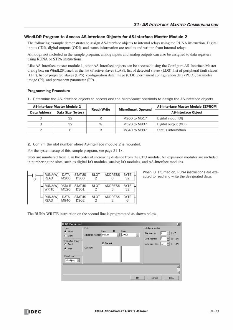
31: AS-INTERFACE MASTER COMMUNICATION
WindLDR Program to Access AS-Interface Objects for AS-Interface Master Module 2The following example demonstrates to assign AS-Interface objects to internal relays using the RUNA instruction. Digital inputs (IDI), digital outputs (ODI), and status information are read to and written from internal relays.
Although not included in the sample program, analog inputs and analog outputs can also be assigned to data registers using RUNA or STPA instructions.
Like AS-Interface master module 1, other AS-Interface objects can be accessed using the Configure AS-Interface Master dialog box on WindLDR, such as the list of active slaves (LAS), list of detected slaves (LDS), list of peripheral fault slaves (LPF), list of projected slaves (LPS), configuration data image (CDI), permanent configuration data (PCD), parameter image (PI), and permanent parameter (PP).
Programming Procedure
1. Determine the AS-Interface objects to access and the MicroSmart operands to assign the AS-Interface objects.
2. Confirm the slot number where AS-Interface module 2 is mounted.
For the system setup of this sample program, see page 31-18.
Slots are numbered from 1, in the order of increasing distance from the CPU module. All expansion modules are included in numbering the slots, such as digital I/O modules, analog I/O modules, and AS-Interface modules.
The RUNA WRITE instruction on the second line is programmed as shown below.
AS-Interface Master Module 2Read/Write MicroSmart Operand
AS-Interface Master Module EEPROM
Data Address Data Size (bytes) AS-Interface Object
0 32 R M200 to M517 Digital input (IDI)
3 32 W M520 to M837 Digital output (ODI)
2 6 R M840 to M897 Status information
When I0 is turned on, RUNA instructions are exe-cuted to read and write the designated data.
I0DATAM200
SLOT2
STATUSD300
BYTE32
ADDRESS0READ
RUNA(W)
DATA RM520
SLOT2
STATUSD301
BYTE32
ADDRESS3WRITE
RUNA(W)
DATAM840
SLOT2
STATUSD302
BYTE6
ADDRESS2READ
RUNA(W)
FC5A MICROSMART USER’S MANUAL 31-33
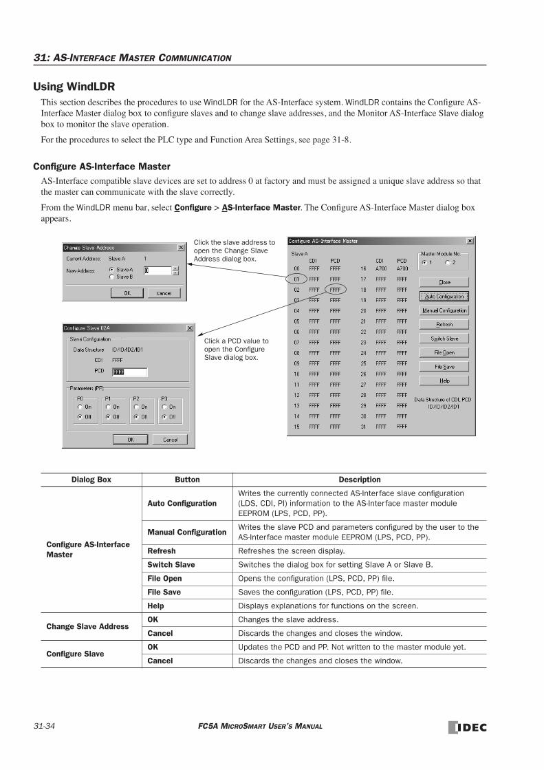
31: AS-INTERFACE MASTER COMMUNICATION
Using WindLDRThis section describes the procedures to use WindLDR for the AS-Interface system. WindLDR contains the Configure AS-Interface Master dialog box to configure slaves and to change slave addresses, and the Monitor AS-Interface Slave dialog box to monitor the slave operation.
For the procedures to select the PLC type and Function Area Settings, see page 31-8.
Configure AS-Interface MasterAS-Interface compatible slave devices are set to address 0 at factory and must be assigned a unique slave address so that the master can communicate with the slave correctly.
From the WindLDR menu bar, select Configure > AS-Interface Master. The Configure AS-Interface Master dialog box appears.
Dialog Box Button Description
Configure AS-Interface Master
Auto ConfigurationWrites the currently connected AS-Interface slave configuration (LDS, CDI, PI) information to the AS-Interface master module EEPROM (LPS, PCD, PP).
Manual ConfigurationWrites the slave PCD and parameters configured by the user to the AS-Interface master module EEPROM (LPS, PCD, PP).
Refresh Refreshes the screen display.
Switch Slave Switches the dialog box for setting Slave A or Slave B.
File Open Opens the configuration (LPS, PCD, PP) file.
File Save Saves the configuration (LPS, PCD, PP) file.
Help Displays explanations for functions on the screen.
Change Slave AddressOK Changes the slave address.
Cancel Discards the changes and closes the window.
Configure SlaveOK Updates the PCD and PP. Not written to the master module yet.
Cancel Discards the changes and closes the window.
Click the slave address to open the Change Slave Address dialog box.
Click a PCD value to open the Configure Slave dialog box.
31-34 FC5A MICROSMART USER’S MANUAL

31: AS-INTERFACE MASTER COMMUNICATION
Slave Address Shading ColorsOperating status of the slave can be confirmed by viewing the shading color at the slave address on the Configure AS-Interface Master dialog box. The screen display can be updated by clicking the Refresh button.
Change Slave AddressWhen a slave is connected to the AS-Interface master module, the slave address can be changed using WindLDR.
To change a slave address, from the WindLDR menu bar, select Configure > AS-Interface Master. The Configure AS-Interface Master dialog box appears.
Click a slave address to open the Change Slave Address dialog box. Select Slave A or Slave B, enter a required address in the New Address field, and click OK. The Change Slave Address dialog box is closed. The new slave address is stored in the slave module nonvolatile memory.
If the command is not processed correctly, the error message “AS-Interface Master Error” and an error code will appear. See page 31-38.
The address cannot be changed in the following cases.
Address Shading DescriptionLASList of active slaves
LDSList of
detected slaves
LPFList of
peripheral fault slaves
LPSList of
projected slaves
No Shade The slave is not recognized by the master. OFF OFF OFF ON/OFF
Blue Shade The slave is active. ON ON OFF ON
Yellow Shade The slave is recognized but not enabled to operate. OFF ON OFF OFF
Red Shade An error was found in the slave. ON/OFF ON/OFF ON ON/OFF
• Duplicate slave addresses
Each slave must have a unique address. Do not connect two or more slaves with the same address, otherwise the AS-Interface master module cannot locate the slave correctly. When two slaves have the same address and different identification codes (ID, I/O, ID2, ID1), the AS-Interface master module detects an error. When two slaves have the same address and same identification codes, the AS-Inter-face master module cannot detect an error. Failure to observe this warning may cause severe personal injury or heavy damage to property.
• When a slave with address 0 is connected to the AS-Interface master module, power up the Micro-Smart CPU module first. Approximately 5 seconds later, turn on the AS-Interface power supply. If the CPU module and AS-Interface power supply are turned on at the same time, the AS-Interface master module enters normal protected offline. In this mode, slave addresses can be changed, but the slave status cannot be confirmed on WindLDR.
Error Code Description
1 • An error was found on the expansion I/O bus.
7 • The AS-Interface master module is in local mode.
8
• The slave you are trying to change does not exist.• A slave of the designated new address already exists.• While a standard slave was set at A address, attempt was made to set an A/B slave at B
address of the same number.• While an A/B slave was set at B address, attempt was made to set a standard slave at A
address of the same number.
Warning
Caution
FC5A MICROSMART USER’S MANUAL 31-35

31: AS-INTERFACE MASTER COMMUNICATION
ConfigurationBefore commissioning the AS-Interface master module, configuration must be done using either WindLDR or the pushbut-tons on the front of the AS-Interface master module. This section describes the method of configuration using WindLDR. For configuration using the pushbuttons, see page 31-10. Configuration is the procedure to store the following information to the AS-Interface master module EEPROM.
• A list of slave addresses to be used• Configuration data to specify slave types, or identification codes (ID, I/O, ID2, ID1)• Parameters (P3, P2, P1, P0) to designate the slave operation at power-up
WindLDR provides two options for configuration: auto configuration to execute automatic configuration and manual con-figuration to execute configuration according to the data selected by the user.
Auto ConfigurationAuto configuration stores the current slave configuration data (LDS, CDI, PI) to the AS-Interface master module EEPROM (LPS, PCD, PP). To execute auto configuration, press Auto Configuration in the Configure AS-Interface Master dialog box. Auto configuration has the same effect as the configuration using the pushbuttons on the AS-Interface master module.
Manual ConfigurationManual configuration is the procedure to write the LPS, PCD, and PP desig-nated on WindLDR to the AS-Interface master module EEPROM. LPS is auto-matically generated by WindLDR based on the value for PCD.
To change PCD and PP, use the Configure Slave dialog box. Set the PCD of each slave to the same value as its CDI. If the PCD is differ-ent from the CDI for a slave, then that slave does not function cor-rectly. Set FFFFh to the PCD of vacant slave numbers.
After entering a PCD value and selecting parameter statuses, click OK. At this point, the configuration data are not stored to the AS- Interface master module EEPROM. To store the changes, click Manual Configuration on the Configure AS-Interface Mas-ter dialog box. The screen display of the Configure AS-Interface Master dialog box can be updated using Refresh.
If you save the configuration data to a file, you can open the file to configure other AS-Interface master modules using the same data. To save and open the configuration file, click File Save or File Open.
If the configuration command is not processed correctly, the error message “AS-Interface Master Error” and an error code will appear. See page 31-38.
If the error message “Configuration failure. Confirm the slave setup, and perform configuration again.” is shown, and the FLT LED is on, then remove the cause of the error, referring to page 31-13, and repeat configuration.
The configuration cannot be done in the following cases.
Slave Configuration Data AS-Interface Master Module EEPROM
List of detected slaves (LDS)Configuration data image (CDI)Parameter image (PI)
List of projected slaves (LPS)Permanent configuration data (PCD)Permanent parameter (PP)
Error Code Description
1 • An error was found on the expansion I/O bus.
2• While the AS-Interface master module was in offline mode, attempt was made to execute auto
configuration or manual configuration.
7• While slave address 0 existed on the bus, attempt was made to execute auto configuration or
manual configuration.• The AS-Interface master module is in local mode.
Configuration
PermanentParameter
(PP)
PCD LPS
FFFFh 0
Other values 1
31-36 FC5A MICROSMART USER’S MANUAL

31: AS-INTERFACE MASTER COMMUNICATION
Monitor AS-Interface SlaveWhile the MicroSmart is communicating with AS-Interface slaves through the AS-Interface bus, operating status of AS-Interface slaves can be monitored using WindLDR on a computer. Output statuses and parameter image (PI) can also be changed using WindLDR.
To open the Monitor AS-Interface Slaves dialog box, from the WindLDR menu bar, select Online > Monitor. From the WindLDR menu bar, select Online, and select Monitor AS-Interface Slaves in the pull-down menu.
Change Slave Output Statuses and ParametersThe output statuses and parameter image (PI) of the slaves connected to the AS-Interface master module can be changed. To open the Slave Status dialog box, click the output of a required slave address in the Monitor AS-Interface Slaves dialog box. Then, click the On or Off button to change the statuses of outputs DO0 through DO3 and parameters P0 through P3 as required. Click Store to save the changes to the slave module.
If the command is not processed correctly, the error message “AS-Interface Master Error” and an error code will appear. See page 31-38.
The output statuses and parameters cannot be changed in the following cases.
Dialog Box Button Description
Monitor AS-Interface Slaves
Switch Slaves Switches between Slave A screen and Slave B screen.
Close Closes the window.
Help Displays explanations for functions on the screen.
Slave StatusStore Stores output statuses and parameters to the slave.
Close Closes the window.
Error Code Description
1 • An error was found on the expansion I/O bus.
7 • The AS-Interface master module is in local mode.
8 • Attempt was made to change the parameters of a slave which did not exist.
Parameter Image
(PI)
FC5A MICROSMART USER’S MANUAL 31-37

31: AS-INTERFACE MASTER COMMUNICATION
Error MessagesWhen an error is returned from the AS-Interface master module, WindLDR will display an error message. The error codes and their meanings are given below.
When a reply message is not returned from the AS-Interface master module, the following error message will be dis-played.
Error Code Description
1 • An error was found on the expansion I/O bus.
2• While the AS-Interface master module was in offline mode, attempt was made to perform auto
configuration or manual configuration.• An incorrect command was sent.
7• While slave address 0 existed on the bus, attempt was made to perform auto configuration or
manual configuration.• The AS-Interface master module is in local mode.
8
• The slave you are trying to change does not exist.• A slave of the designated new address already exists.• While a standard slave was set at A address, attempt was made to set an A/B slave at B
address of the same number.• While an A/B slave was set at B address, attempt was made to set a standard slave at A
address of the same number.• Attempt was made to change the parameters of a slave which did not exist.
31-38 FC5A MICROSMART USER’S MANUAL

31: AS-INTERFACE MASTER COMMUNICATION
SwitchNet Data I/O Port (AS-Interface Master Module 1)SwitchNet control units can be used as slaves in the AS-Interface network and are available in ø16mm L6 series and ø22mm HW series. Input signals to the MicroSmart AS-Interface master module are read to internal relays allocated to each input point designated by a slave number and a DI number. Similarly, output signals from the MicroSmart AS-Inter-face master module are written to internal relays allocated to each output point designated by a slave number and a DO number. When programming a ladder diagram for the MicroSmart, use internal relays allocated to input signals and output signals of SwitchNet control units.
L6 series and HW series SwitchNet control units have slightly different digital I/O data allocations.
L6 Series Digital I/O Data Allocation
Input data is sent from slaves to the AS-Interface master. Output data is sent from the AS-Interface master to slaves.
Notes:
SwitchNet L6 SeriesSlave Unit Used I/O
Input Data(slave send data)
Output Data(slave receive data)
DI3 DI2 DI1 DI0 DO3 DO2 DO1 DO0
Pushbutton 1 in 0 X1 1 1 * — — —
Pilot light 1 out 0 0 1 1 * — — X1
Illuminated pushbutton 1 in/1 out 0 X1 1 1 * — — X1
Selector, Key selector, Lever: 2-position 1 in 0 X2 1 1 * — — —
Selector, Key selector, Lever: 3-position 2 in X3 X3 1 1 * — — —
Illuminated selector: 2-position 1 in/1 out 0 X2 1 1 * — — X1
Illuminated selector: 3-position 2 in/1 out X3 X3 1 1 * — — X1
1. ∗ The AS-Interface master uses bit DO3 for addressing A/B slaves.
2. In the above table, bits marked with X1, X2, and X3 are used for SwitchNet I/O data.
3. X1: When pushbutton is pressed, input data is 1 (on). When not pressed, input data is 0 (off). When output data is 1 (on), LED is on. When output data is 0 (off), LED is off.
4. X2: The input data from 2-position selector, key selector, and illuminated selector switches and 2-position lever switches depend on the operator position as shown below.
5. X3: The input data from 3-position selector, key selector, and illuminated selector switches and 3-position lever switches depend on the operator position as shown below.
6. Unused input bits DI3 and DI2 are 0 (off), and unused input bits DI1 and DI0 are 1 (on). Slaves ignore unused output data (—) sent from the master.
2-position Operator
Operator Position Left/Down Right/Up
DI2 0 1
Selector
Left Right Up
Down
Lever
3-position Operator
Operator Position Left/Down Center Right/Up
DI3 0 0 1
DI2 1 0 0
Selector
Left RightCenter Up
Center
Down
Lever
• Write_Parameter Command • Write_Parameter Settings
0 0 A4 A3 A2 A1 A0 1 SelP3 P2 P1 P0 PB 1
LED Brightness
Settings
RemarksOutput Selection Control Data
P2 P1 P0
100%
1: DO00: DO1
1 1 Default
50% 0 1
25% 1 0
12.5% 0 0
FC5A MICROSMART USER’S MANUAL 31-39

31: AS-INTERFACE MASTER COMMUNICATION
HW Series Digital I/O Data Allocation
Input data is sent from slaves to the AS-Interface master. Output data is sent from the AS-Interface master to slaves.
Notes:
SwitchNet HW SeriesSlave Unit Used I/O
Communication Block Mounting
Position
Input Data(slave send data)
Output Data(slave receive data)
DI3 DI2 DI1 DI0 DO3 DO2 DO1 DO0
Pushbutton 1 in ➁ 0 X1 1 1 * — — —
Pilot light 1 out ➁ 0 0 1 1 * — — X1
Illuminated pushbutton 1 in/1 out ➁ 0 X1 1 1 * — — X1
Selector, Key selector: 2-position 1 in ➁ 0 X2 1 1 * — — —
Selector, Key selector: 3-position1 in ➀ 0 X3 1 1 * — — —
1 in ➁ 0 X3 1 1 * — — —
Illuminated selector: 2-position 1 in/1 out ➁ 0 X2 1 1 * — — X1
Illuminated selector: 3-position1 in ➀ 0 X3 1 1 * — — —
1 in/1 out ➁ 0 X3 1 1 * — — X1
1. ∗ The AS-Interface master uses bit DO3 for addressing A/B slaves.
2. In the above table, bits marked with X1, X2, and X3 are used for SwitchNet I/O data.
3. X1: When pushbutton is pressed, input data is 1 (on). When not pressed, input data is 0 (off). When output data is 1 (on), LED is on. When output data is 0 (off), LED is off.
4. X2: The input data from 2-position selector, key selector, and illuminated selector switches depend on the operator position as shown below.
5. X3: The input data from 3-position selector, key selector, and illuminated selector switches depend on the operator position as shown below.
As shown in the table and figure, 3-position selector, key selector, and illuminated selector switches use two communi-cation blocks. Each communication block must have a unique address, therefore the 3-position selectors require 2 slave addresses.
6. Unused input bits DI3 and DI2 are 0 (off), and unused input bits DI1 and DI0 are 1 (on). Slaves ignore unused output data (—) sent from the master.
2-position Operator
Operator Position Left Right
DI2 0 1
3-position Operator
Operator Position Left Center Right
Communication Block Mounting
PositionInput Data Bit
➀ DI2 1 0 0
➁ DI2 0 0 1
SelectorLeft Right
Selector
Left RightCenter
Address Marking Area
MountingPosition ➀
MountingPosition ➁
AS-Interface –
AS-Interface +
AS-Interface +
AS-Interface –
Communication Block Mounting Position(Rear View)
On 3-position selector, key selector, and illuminated selector switches, communication blocks ➀ and ➁ are mounted in positions shown above.
• Write_Parameter Command • Write_Parameter Settings
0 0 A4 A3 A2 A1 A0 1 SelP3 P2 P1 P0 PB 1
LED Brightness
Settings
RemarksOutput Selection Control Data
P2 P1 P0
100%
1: DO00: DO1
1 1 Default
50% 0 1
25% 1 0
12.5% 0 0
31-40 FC5A MICROSMART USER’S MANUAL

31: AS-INTERFACE MASTER COMMUNICATION
•Internal Relays for SwitchNet Slaves (AS-Interface Master Module 1)
L6 Series
Slave NumberPushbutton Pilot Light Illuminated Pushbutton Selector, Key selector,
Lever: 2-positionInput DI2 Output DO0 Input DI2 Output DO0 Input DI2
(Slave 0) M1302 M1620 M1302 M1620 M1302Slave 1(A) M1306 M1624 M1306 M1624 M1306Slave 2(A) M1312 M1630 M1312 M1630 M1312Slave 3(A) M1316 M1634 M1316 M1634 M1316Slave 4(A) M1322 M1640 M1322 M1640 M1322Slave 5(A) M1326 M1644 M1326 M1644 M1326Slave 6(A) M1332 M1650 M1332 M1650 M1332Slave 7(A) M1336 M1654 M1336 M1654 M1336Slave 8(A) M1342 M1660 M1342 M1660 M1342Slave 9(A) M1346 M1664 M1346 M1664 M1346Slave 10(A) M1352 M1670 M1352 M1670 M1352Slave 11(A) M1356 M1674 M1356 M1674 M1356Slave 12(A) M1362 M1680 M1362 M1680 M1362Slave 13(A) M1366 M1684 M1366 M1684 M1366Slave 14(A) M1372 M1690 M1372 M1690 M1372Slave 15(A) M1376 M1694 M1376 M1694 M1376Slave 16(A) M1382 M1700 M1382 M1700 M1382Slave 17(A) M1386 M1704 M1386 M1704 M1386Slave 18(A) M1392 M1710 M1392 M1710 M1392Slave 19(A) M1396 M1714 M1396 M1714 M1396Slave 20(A) M1402 M1720 M1402 M1720 M1402Slave 21(A) M1406 M1724 M1406 M1724 M1406Slave 22(A) M1412 M1730 M1412 M1730 M1412Slave 23(A) M1416 M1734 M1416 M1734 M1416Slave 24(A) M1422 M1740 M1422 M1740 M1422Slave 25(A) M1426 M1744 M1426 M1744 M1426Slave 26(A) M1432 M1750 M1432 M1750 M1432Slave 27(A) M1436 M1754 M1436 M1754 M1436Slave 28(A) M1442 M1760 M1442 M1760 M1442Slave 29(A) M1446 M1764 M1446 M1764 M1446Slave 30(A) M1452 M1770 M1452 M1770 M1452Slave 31(A) M1456 M1774 M1456 M1774 M1456Slave 1B M1466 M1784 M1466 M1784 M1466Slave 2B M1472 M1790 M1472 M1790 M1472Slave 3B M1476 M1794 M1476 M1794 M1476Slave 4B M1482 M1800 M1482 M1800 M1482Slave 5B M1486 M1804 M1486 M1804 M1486Slave 6B M1492 M1810 M1492 M1810 M1492Slave 7B M1496 M1814 M1496 M1814 M1496Slave 8B M1502 M1820 M1502 M1820 M1502Slave 9B M1506 M1824 M1506 M1824 M1506Slave 10B M1512 M1830 M1512 M1830 M1512Slave 11B M1516 M1834 M1516 M1834 M1516Slave 12B M1522 M1840 M1522 M1840 M1522Slave 13B M1526 M1844 M1526 M1844 M1526Slave 14B M1532 M1850 M1532 M1850 M1532Slave 15B M1536 M1854 M1536 M1854 M1536Slave 16B M1542 M1860 M1542 M1860 M1542Slave 17B M1546 M1864 M1546 M1864 M1546Slave 18B M1552 M1870 M1552 M1870 M1552Slave 19B M1556 M1874 M1556 M1874 M1556Slave 20B M1562 M1880 M1562 M1880 M1562Slave 21B M1566 M1884 M1566 M1884 M1566Slave 22B M1572 M1890 M1572 M1890 M1572Slave 23B M1576 M1894 M1576 M1894 M1576Slave 24B M1582 M1900 M1582 M1900 M1582Slave 25B M1586 M1904 M1586 M1904 M1586Slave 26B M1592 M1910 M1592 M1910 M1592Slave 27B M1596 M1914 M1596 M1914 M1596Slave 28B M1602 M1920 M1602 M1920 M1602Slave 29B M1606 M1924 M1606 M1924 M1606Slave 30B M1612 M1930 M1612 M1930 M1612Slave 31B M1616 M1934 M1616 M1934 M1616
FC5A MICROSMART USER’S MANUAL 31-41

31: AS-INTERFACE MASTER COMMUNICATION
L6 Series (continued)
Slave NumberSelector, Key selector, Lever:
3-position Illuminated selector: 2-position Illuminated selector: 3-position
Input DI3 Input DI2 Input DI2 Output DO0 Input DI3 Input DI2 Output DO0(Slave 0) M1303 M1302 M1302 M1620 M1303 M1302 M1620Slave 1(A) M1307 M1306 M1306 M1624 M1307 M1306 M1624Slave 2(A) M1313 M1312 M1312 M1630 M1313 M1312 M1630Slave 3(A) M1317 M1316 M1316 M1634 M1317 M1316 M1634Slave 4(A) M1323 M1322 M1322 M1640 M1323 M1322 M1640Slave 5(A) M1327 M1326 M1326 M1644 M1327 M1326 M1644Slave 6(A) M1333 M1332 M1332 M1650 M1333 M1332 M1650Slave 7(A) M1337 M1336 M1336 M1654 M1337 M1336 M1654Slave 8(A) M1343 M1342 M1342 M1660 M1343 M1342 M1660Slave 9(A) M1347 M1346 M1346 M1664 M1347 M1346 M1664Slave 10(A) M1353 M1352 M1352 M1670 M1353 M1352 M1670Slave 11(A) M1357 M1356 M1356 M1674 M1357 M1356 M1674Slave 12(A) M1363 M1362 M1362 M1680 M1363 M1362 M1680Slave 13(A) M1367 M1366 M1366 M1684 M1367 M1366 M1684Slave 14(A) M1373 M1372 M1372 M1690 M1373 M1372 M1690Slave 15(A) M1377 M1376 M1376 M1694 M1377 M1376 M1694Slave 16(A) M1383 M1382 M1382 M1700 M1383 M1382 M1700Slave 17(A) M1387 M1386 M1386 M1704 M1387 M1386 M1704Slave 18(A) M1393 M1392 M1392 M1710 M1393 M1392 M1710Slave 19(A) M1397 M1396 M1396 M1714 M1397 M1396 M1714Slave 20(A) M1403 M1402 M1402 M1720 M1403 M1402 M1720Slave 21(A) M1407 M1406 M1406 M1724 M1407 M1406 M1724Slave 22(A) M1413 M1412 M1412 M1730 M1413 M1412 M1730Slave 23(A) M1417 M1416 M1416 M1734 M1417 M1416 M1734Slave 24(A) M1423 M1422 M1422 M1740 M1423 M1422 M1740Slave 25(A) M1427 M1426 M1426 M1744 M1427 M1426 M1744Slave 26(A) M1433 M1432 M1432 M1750 M1433 M1432 M1750Slave 27(A) M1437 M1436 M1436 M1754 M1437 M1436 M1754Slave 28(A) M1443 M1442 M1442 M1760 M1443 M1442 M1760Slave 29(A) M1447 M1446 M1446 M1764 M1447 M1446 M1764Slave 30(A) M1453 M1452 M1452 M1770 M1453 M1452 M1770Slave 31(A) M1457 M1456 M1456 M1774 M1457 M1456 M1774Slave 1B M1467 M1466 M1466 M1784 M1467 M1466 M1784Slave 2B M1473 M1472 M1472 M1790 M1473 M1472 M1790Slave 3B M1477 M1476 M1476 M1794 M1477 M1476 M1794Slave 4B M1483 M1482 M1482 M1800 M1483 M1482 M1800Slave 5B M1487 M1486 M1486 M1804 M1487 M1486 M1804Slave 6B M1493 M1492 M1492 M1810 M1493 M1492 M1810Slave 7B M1497 M1496 M1496 M1814 M1497 M1496 M1814Slave 8B M1503 M1502 M1502 M1820 M1503 M1502 M1820Slave 9B M1507 M1506 M1506 M1824 M1507 M1506 M1824Slave 10B M1513 M1512 M1512 M1830 M1513 M1512 M1830Slave 11B M1517 M1516 M1516 M1834 M1517 M1516 M1834Slave 12B M1523 M1522 M1522 M1840 M1523 M1522 M1840Slave 13B M1527 M1526 M1526 M1844 M1527 M1526 M1844Slave 14B M1533 M1532 M1532 M1850 M1533 M1532 M1850Slave 15B M1537 M1536 M1536 M1854 M1537 M1536 M1854Slave 16B M1543 M1542 M1542 M1860 M1543 M1542 M1860Slave 17B M1547 M1546 M1546 M1864 M1547 M1546 M1864Slave 18B M1553 M1552 M1552 M1870 M1553 M1552 M1870Slave 19B M1557 M1556 M1556 M1874 M1557 M1556 M1874Slave 20B M1563 M1562 M1562 M1880 M1563 M1562 M1880Slave 21B M1567 M1566 M1566 M1884 M1567 M1566 M1884Slave 22B M1573 M1572 M1572 M1890 M1573 M1572 M1890Slave 23B M1577 M1576 M1576 M1894 M1577 M1576 M1894Slave 24B M1583 M1582 M1582 M1900 M1583 M1582 M1900Slave 25B M1587 M1586 M1586 M1904 M1587 M1586 M1904Slave 26B M1593 M1592 M1592 M1910 M1593 M1592 M1910Slave 27B M1597 M1596 M1596 M1914 M1597 M1596 M1914Slave 28B M1603 M1602 M1602 M1920 M1603 M1602 M1920Slave 29B M1607 M1606 M1606 M1924 M1607 M1606 M1924Slave 30B M1613 M1612 M1612 M1930 M1613 M1612 M1930Slave 31B M1617 M1616 M1616 M1934 M1617 M1616 M1934
31-42 FC5A MICROSMART USER’S MANUAL

31: AS-INTERFACE MASTER COMMUNICATION
HW Series
Slave NumberPushbutton Pilot Light Illuminated Pushbutton Selector, Key selector:
2-positionInput DI2 Output DO0 Input DI2 Output DO0 Input DI2
(Slave 0) M1302 M1620 M1302 M1620 M1302Slave 1(A) M1306 M1624 M1306 M1624 M1306Slave 2(A) M1312 M1630 M1312 M1630 M1312Slave 3(A) M1316 M1634 M1316 M1634 M1316Slave 4(A) M1322 M1640 M1322 M1640 M1322Slave 5(A) M1326 M1644 M1326 M1644 M1326Slave 6(A) M1332 M1650 M1332 M1650 M1332Slave 7(A) M1336 M1654 M1336 M1654 M1336Slave 8(A) M1342 M1660 M1342 M1660 M1342Slave 9(A) M1346 M1664 M1346 M1664 M1346Slave 10(A) M1352 M1670 M1352 M1670 M1352Slave 11(A) M1356 M1674 M1356 M1674 M1356Slave 12(A) M1362 M1680 M1362 M1680 M1362Slave 13(A) M1366 M1684 M1366 M1684 M1366Slave 14(A) M1372 M1690 M1372 M1690 M1372Slave 15(A) M1376 M1694 M1376 M1694 M1376Slave 16(A) M1382 M1700 M1382 M1700 M1382Slave 17(A) M1386 M1704 M1386 M1704 M1386Slave 18(A) M1392 M1710 M1392 M1710 M1392Slave 19(A) M1396 M1714 M1396 M1714 M1396Slave 20(A) M1402 M1720 M1402 M1720 M1402Slave 21(A) M1406 M1724 M1406 M1724 M1406Slave 22(A) M1412 M1730 M1412 M1730 M1412Slave 23(A) M1416 M1734 M1416 M1734 M1416Slave 24(A) M1422 M1740 M1422 M1740 M1422Slave 25(A) M1426 M1744 M1426 M1744 M1426Slave 26(A) M1432 M1750 M1432 M1750 M1432Slave 27(A) M1436 M1754 M1436 M1754 M1436Slave 28(A) M1442 M1760 M1442 M1760 M1442Slave 29(A) M1446 M1764 M1446 M1764 M1446Slave 30(A) M1452 M1770 M1452 M1770 M1452Slave 31(A) M1456 M1774 M1456 M1774 M1456Slave 1B M1466 M1784 M1466 M1784 M1466Slave 2B M1472 M1790 M1472 M1790 M1472Slave 3B M1476 M1794 M1476 M1794 M1476Slave 4B M1482 M1800 M1482 M1800 M1482Slave 5B M1486 M1804 M1486 M1804 M1486Slave 6B M1492 M1810 M1492 M1810 M1492Slave 7B M1496 M1814 M1496 M1814 M1496Slave 8B M1502 M1820 M1502 M1820 M1502Slave 9B M1506 M1824 M1506 M1824 M1506Slave 10B M1512 M1830 M1512 M1830 M1512Slave 11B M1516 M1834 M1516 M1834 M1516Slave 12B M1522 M1840 M1522 M1840 M1522Slave 13B M1526 M1844 M1526 M1844 M1526Slave 14B M1532 M1850 M1532 M1850 M1532Slave 15B M1536 M1854 M1536 M1854 M1536Slave 16B M1542 M1860 M1542 M1860 M1542Slave 17B M1546 M1864 M1546 M1864 M1546Slave 18B M1552 M1870 M1552 M1870 M1552Slave 19B M1556 M1874 M1556 M1874 M1556Slave 20B M1562 M1880 M1562 M1880 M1562Slave 21B M1566 M1884 M1566 M1884 M1566Slave 22B M1572 M1890 M1572 M1890 M1572Slave 23B M1576 M1894 M1576 M1894 M1576Slave 24B M1582 M1900 M1582 M1900 M1582Slave 25B M1586 M1904 M1586 M1904 M1586Slave 26B M1592 M1910 M1592 M1910 M1592Slave 27B M1596 M1914 M1596 M1914 M1596Slave 28B M1602 M1920 M1602 M1920 M1602Slave 29B M1606 M1924 M1606 M1924 M1606Slave 30B M1612 M1930 M1612 M1930 M1612Slave 31B M1616 M1934 M1616 M1934 M1616
FC5A MICROSMART USER’S MANUAL 31-43
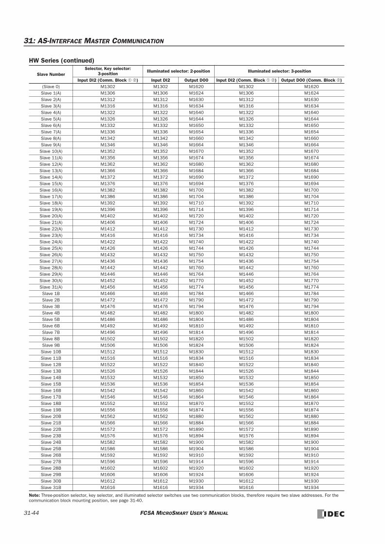
31: AS-INTERFACE MASTER COMMUNICATION
HW Series (continued)
Note: Three-position selector, key selector, and illuminated selector switches use two communication blocks, therefore require two slave addresses. For the communication block mounting position, see page 31-40.
Slave NumberSelector, Key selector:
3-position Illuminated selector: 2-position Illuminated selector: 3-position
Input DI2 (Comm. Block ➀ ➁) Input DI2 Output DO0 Input DI2 (Comm. Block ➀ ➁) Output DO0 (Comm. Block ➁)(Slave 0) M1302 M1302 M1620 M1302 M1620Slave 1(A) M1306 M1306 M1624 M1306 M1624Slave 2(A) M1312 M1312 M1630 M1312 M1630Slave 3(A) M1316 M1316 M1634 M1316 M1634Slave 4(A) M1322 M1322 M1640 M1322 M1640Slave 5(A) M1326 M1326 M1644 M1326 M1644Slave 6(A) M1332 M1332 M1650 M1332 M1650Slave 7(A) M1336 M1336 M1654 M1336 M1654Slave 8(A) M1342 M1342 M1660 M1342 M1660Slave 9(A) M1346 M1346 M1664 M1346 M1664Slave 10(A) M1352 M1352 M1670 M1352 M1670Slave 11(A) M1356 M1356 M1674 M1356 M1674Slave 12(A) M1362 M1362 M1680 M1362 M1680Slave 13(A) M1366 M1366 M1684 M1366 M1684Slave 14(A) M1372 M1372 M1690 M1372 M1690Slave 15(A) M1376 M1376 M1694 M1376 M1694Slave 16(A) M1382 M1382 M1700 M1382 M1700Slave 17(A) M1386 M1386 M1704 M1386 M1704Slave 18(A) M1392 M1392 M1710 M1392 M1710Slave 19(A) M1396 M1396 M1714 M1396 M1714Slave 20(A) M1402 M1402 M1720 M1402 M1720Slave 21(A) M1406 M1406 M1724 M1406 M1724Slave 22(A) M1412 M1412 M1730 M1412 M1730Slave 23(A) M1416 M1416 M1734 M1416 M1734Slave 24(A) M1422 M1422 M1740 M1422 M1740Slave 25(A) M1426 M1426 M1744 M1426 M1744Slave 26(A) M1432 M1432 M1750 M1432 M1750Slave 27(A) M1436 M1436 M1754 M1436 M1754Slave 28(A) M1442 M1442 M1760 M1442 M1760Slave 29(A) M1446 M1446 M1764 M1446 M1764Slave 30(A) M1452 M1452 M1770 M1452 M1770Slave 31(A) M1456 M1456 M1774 M1456 M1774Slave 1B M1466 M1466 M1784 M1466 M1784Slave 2B M1472 M1472 M1790 M1472 M1790Slave 3B M1476 M1476 M1794 M1476 M1794Slave 4B M1482 M1482 M1800 M1482 M1800Slave 5B M1486 M1486 M1804 M1486 M1804Slave 6B M1492 M1492 M1810 M1492 M1810Slave 7B M1496 M1496 M1814 M1496 M1814Slave 8B M1502 M1502 M1820 M1502 M1820Slave 9B M1506 M1506 M1824 M1506 M1824Slave 10B M1512 M1512 M1830 M1512 M1830Slave 11B M1516 M1516 M1834 M1516 M1834Slave 12B M1522 M1522 M1840 M1522 M1840Slave 13B M1526 M1526 M1844 M1526 M1844Slave 14B M1532 M1532 M1850 M1532 M1850Slave 15B M1536 M1536 M1854 M1536 M1854Slave 16B M1542 M1542 M1860 M1542 M1860Slave 17B M1546 M1546 M1864 M1546 M1864Slave 18B M1552 M1552 M1870 M1552 M1870Slave 19B M1556 M1556 M1874 M1556 M1874Slave 20B M1562 M1562 M1880 M1562 M1880Slave 21B M1566 M1566 M1884 M1566 M1884Slave 22B M1572 M1572 M1890 M1572 M1890Slave 23B M1576 M1576 M1894 M1576 M1894Slave 24B M1582 M1582 M1900 M1582 M1900Slave 25B M1586 M1586 M1904 M1586 M1904Slave 26B M1592 M1592 M1910 M1592 M1910Slave 27B M1596 M1596 M1914 M1596 M1914Slave 28B M1602 M1602 M1920 M1602 M1920Slave 29B M1606 M1606 M1924 M1606 M1924Slave 30B M1612 M1612 M1930 M1612 M1930Slave 31B M1616 M1616 M1934 M1616 M1934
31-44 FC5A MICROSMART USER’S MANUAL

32: TROUBLESHOOTING
IntroductionThis chapter describes the procedures to determine the cause of trouble and actions to be taken when any trouble occurs while operating the MicroSmart.
The MicroSmart has self-diagnostic functions to prevent the spread of troubles if any trouble should occur. In case of any trouble, follow the troubleshooting procedures to determine the cause and to correct the error.
Errors are checked in various stages. While editing a user program on WindLDR, incorrect operands and other data are rejected. User program syntax errors are found during compilation on WindLDR. When an incorrect program is down-loaded to the MicroSmart, user program syntax errors are still checked. Errors are also checked at starting and during operation of the MicroSmart. When an error occurs, the error is reported by turning on the ERR LED on the MicroSmart and an error message can be viewed on WindLDR. Error codes can also be read on the HMI module.
ERR LEDThe MicroSmart CPU module has an error indicator ERR. When an error occurs in the MicroSmart CPU module, the ERR LED is lit. See the trouble shooting diagrams on page 32-10.
For error causes to turn on the ERR LED, see page 32-4.
Reading Error DataWhen any error occurs during the MicroSmart operation, “Error” is indicated and error details can be read using WindLDR on a computer.
Monitoring WindLDR
1. From the WindLDR menu bar, select Online > Monitor. The monitor mode is enabled.
2. From the WindLDR menu bar, select Online > PLC Status. The PLC Status dialog box appears.
When any error exists, “Error” is displayed in the error status box.
PWR
RUN
ERR
STAT
0 1 2 3 4 5 7 106 11
0 1 2 3 4 5 6 7 10 11 12 13 14 15
OUT
IN
ERR LED
Error Status BoxD8005 (general error code)
Details Button
System Program VersionD8029
FC5A MICROSMART USER’S MANUAL 32-1

32: TROUBLESHOOTING
3. Under the Error Status in the PLC Status dialog box, click the Details button. The PLC Error Status screen appears.
Clearing Error Codes from WindLDRAfter removing the cause of the error, clear the error code using the following procedure:
1. From the WindLDR menu bar, select Online > Monitor. The monitor mode is enabled.
2. From the WindLDR menu bar, select Online > PLC Status. The PLC Status dialog box appears.
3. Under the Error Status in the PLC Status dialog box, click the Clear button.
This procedure clears the error code from special data register D8005 (general error code), and the error is cleared from the PLC Status dialog box.
Clear ButtonError Cleared
32-2 FC5A MICROSMART USER’S MANUAL

32: TROUBLESHOOTING
Special Data Registers for Error InformationTwo data registers are assigned to store information on errors.
General Error CodesThe general error code is stored to special data register D8005 (general error code).
When monitoring the PLC status using WindLDR, the error code is displayed in the error code box under the Error Status in the PLC Status dialog box using four hexadecimal digits 0 through F. Each digit of the error code indicates a different set of conditions requiring attention. After the error code is cleared as described on the preceding page, the error code box is left blank.
For example, the error code may read out “0021.” This indicates two conditions requiring attention, “User program sum check error” from the third chart and “Power failure” from the fourth chart. If the read-out displays “000D,” this indicates three conditions exist from only the fourth chart.
D8005 General Error Code
D8006 User Program Execution Error Code
Error Code: Most Significant Digit F000 E000 D000 C000 B000 A000 9000 8000 7000 6000 5000 4000 3000 2000 1000 0000
I/O bus initialize error X
Error Code: 2nd Digit from Left F00 E00 D00 C00 B00 A00 900 800 700 600 500 400 300 200 100 000
User program writing error X X X X X X X X
CPU module error X X X X X X X X
Clock IC error X X X X X X X X
Error Code: 3rd Digit from Left F0 E0 D0 C0 B0 A0 90 80 70 60 50 40 30 20 10 00
TIM/CNT preset value sum check error X X X X X X X X
User program RAM sum check error X X X X X X X X
Keep data error X X X X X X X X
User program syntax error X X X X X X X X
Error Code: Least Significant Digit F E D C B A 9 8 7 6 5 4 3 2 1 0
Power failure X X X X X X X X
Watchdog timer error X X X X X X X X
Data link connection error X X X X X X X X
User program EEPROM sum check error X X X X X X X X
FC5A MICROSMART USER’S MANUAL 32-3

32: TROUBLESHOOTING
CPU Module Operating Status, Output, and ERR LED during Errors
*1: When a program RAM sum check error occurs, operation is stopped momentarily for reloading the user program. After completing the reloading, operation resumes.
*2: Operation starts to run and outputs are turned on or off according to the user program as default, but it is also possible to stop operation and turn off outputs using the Function Area Settings on WindLDR. See page 5-3.
Error Causes and Actions
0001h: Power FailureThis error indicates when the power supply is lower than the specified voltage. This error is also recorded when the power is turned off. Clear the error code using the HMI module or WindLDR on a computer.
0002h: Watchdog Timer ErrorThe watchdog timer monitors the time required for one program cycle (scan time). When the time exceeds approximately 340 ms, the watchdog timer indicates an error. Clear the error code using the HMI module or WindLDR on a computer. If this error occurs frequently, the MicroSmart CPU module has to be replaced.
0004h: Data Link Connection ErrorThis error indicates that the Function Area Settings for data link communication are incorrect or the cable is not connected correctly. Make sure that slave stations are set to station numbers 1 through 31 using WindLDR. No duplication of station numbers is allowed. See page 27-7.
To correct this error, make corrections in the Function Area Settings and download the user program to each station, or connect the cable correctly. Turn power off and on again for the slave station. Then take one of the following actions:
• Turn power off and on for the master station.• Initialize data link communication for the master station using WindLDR on a computer. See page 27-11.• Turn on special internal relay M8007 (data link communication initialize flag) at the master station. See page 27-6.
0008h: User Program EEPROM Sum Check ErrorThe user program stored in the MicroSmart CPU module EEPROM is broken. Download a correct user program to the MicroSmart, and clear the error code using the HMI module or WindLDR on a computer.
When a memory cartridge is installed on the CPU module, the user program in the memory cartridge is checked.
0010h: Timer/Counter Preset Value Sum Check ErrorThe execution data of timer/counter preset values is broken. The timer/counter preset values are initialized to the values of the user program automatically. Note that changed preset values are cleared and that the original values are restored. Clear the error code using the HMI module or WindLDR on a computer.
Error ItemsOperating
StatusOutput ERR LED Checked at
Power failure Stop OFF OFF Any time
Watchdog timer error Stop OFF ON Any time
Data link connection error Stop OFF OFF Initializing data link
User program EEPROM sum check error Stop OFF ON Starting operation
TIM/CNT preset value sum check error Maintained Maintained OFF Starting operation
User program RAM sum check error Stop *1 OFF ON During operation
Keep data errorMaintained/
Stop *2Maintained/
OFF *2OFF Turning power on
User program syntax error Stop OFF ON Downloading user program
User program writing error Stop OFF ON Downloading user program
CPU module error Stop OFF ON Turning power on
Clock IC error Maintained Maintained ON Any time
I/O bus initialize error Stop OFF ON Turning power on
User program execution error Maintained Maintained ON Executing user program
32-4 FC5A MICROSMART USER’S MANUAL

32: TROUBLESHOOTING
0020h: User Program RAM Sum Check ErrorThe data of the user program compile area in the MicroSmart CPU module RAM is broken.When this error occurs, the user program is recompiled automatically, and the timer/counter preset values and expansion data register preset values are initialized to the values of the user program. Note that changed preset values are cleared and that the original values are restored. Clear the error code using the HMI module or WindLDR on a computer.
0040h: Keep Data ErrorThis error indicates that the data designated to be maintained during power failure is broken because of memory backup failure. Note that the “keep” data of internal relays and shift registers are cleared. Data of counters and data registers are also cleared. Clear the error code using the HMI module or WindLDR on a computer.
If this error occurs in a short period of power interruption after the battery has been charged as specified, the battery is defective and the CPU module has to be replaced.
0080h: User Program Syntax ErrorThis error indicates that the user program has a syntax error. Correct the user program, and download the corrected user program to the MicroSmart. The error code is cleared when a correct user program is transferred.
0100h: User Program Writing ErrorThis error indicates a failure of writing into the MicroSmart CPU module EEPROM when downloading a user program. The error code is cleared when writing into the EEPROM is completed successfully. If this error occurs frequently, the MicroSmart CPU module has to be replaced.
When a memory cartridge is installed on the CPU module, writing into the memory cartridge is checked.
0200h: CPU Module ErrorThis error is issued when the EEPROM is not found. When this error occurred, turn power off and on. Clear the error code using the HMI module or WindLDR on a computer. If this error occurs frequently, the MicroSmart CPU module has to be replaced.
0400h: Clock IC ErrorThis error indicates that the real time calendar/clock in the clock cartridge has lost clock backup data or has an error caused by invalid clock data.
Clear the error code and set the calendar/clock data using the HMI module or WindLDR on a computer. The clock cartridge will recover from the error. If the error continues, the clock cartridge has to be replaced. See Troubleshooting Diagram on page 32-17.
2000h: I/O Bus Initialize ErrorThis error indicates that an I/O module has a fault. If this error occurs frequently or normal I/O function is not restored automatically, the I/O module has to be replaced.
FC5A MICROSMART USER’S MANUAL 32-5

32: TROUBLESHOOTING
User Program Execution ErrorThis error indicates that invalid data is found during execution of a user program. When this error occurs, the ERR LED and special internal relay M8004 (user program execution error) are also turned on. The detailed information of this error can be viewed from the error code stored in special data register D8006 (user program execution error code).
User Program Execution Error Code
(D8006)Error Details
1 Source/destination operand is out of range
2 MUL result is out of data type range.
3 DIV result is out of data type range, or division by 0.
4 BCDLS has S1 or S1+1 exceeding 9999.
5 HTOB(W) has S1 exceeding 9999.
6 BTOH has any digit of S1 exceeding 9.
7 HTOA/ATOH/BTOA/ATOB has quantity of digits to convert out of range.
8 ATOH/ATOB has non-ASCII data for S1 through S1+4.
9
WKTIM has S1, S2, and S3 exceeding the valid range.S1: 0 through 127S2/S3: Hour data 0 through 23, minute data 0 through 59S2/S3 can be 10000.
WKTBL instruction is not programmed or WKTIM instruction is executed before WKTBL instruc-tion when 1 (additional days in the week table) or 2 (skip days in the week table) is set for MODE in the WKTIM instruction.
10WKTBL has S1 through Sn out of range.Month: 01 through 12Day: 01 through 31
11 DGRD data exceeds 65535 with BCD5 digits selected.
12CVXTY/CVYTX is executed without matching XYFS.XYFS and CVXTY/CVYTX have the same S1, but have different data types.
13 CVXTY/CVYTX has S2 exceeding the value specified in XYFS.
14 Label in LJMP/LCAL is not found.
15 TXD/RXD is executed while the RS232C port 1 or 2 is not set to user communication mode.
16 PID instruction execution error (see page 21-4).
17 Preset value is written to a timer/counter whose preset value is designated with a data register.
18
Attempt was made to execute an instruction that cannot be used in an interrupt program: SOTU, SOTD, TML, TIM, TMH, TMS, CNT, CDP, CUD, SFR, SFRN, WKTIM, WKTBL, DISP, DGRD, TXD, RXD, DI, EI, XYFS, CVXTY, CVYTX, PULS, PWM, RAMP, ZRN, PID, DTML, DTIM, DTMH, DTMS, TTIM, RUNA, and STPA (see page 5-34).
19 Attempt was made to execute an instruction that is not available for the PLC.
20 PULS, PWM, RAMP, or ZRN has an invalid value in control registers.
21 DECO has S1 exceeding 255.
22 BCNT has S2 exceeding 256.
23 ICMP>= has S1 < S3.
24 — Reserved —
25 BCDLS has S2 exceeding 7.
26DI or EI is executed when interrupt input or timer interrupt is not programmed in the Function Area Settings.
27 Work area is broken when using DTML, DTIM, DTMH, DTMS, or TTIM.
28 S1 for trigonometric function instruction is invalid.
29 Result of F (float) data type instruction is out of the data type range.
30 N_B for SFTL/SFTR is out of range.
32-6 FC5A MICROSMART USER’S MANUAL

32: TROUBLESHOOTING
Troubleshooting Diagrams
When one of the following problems is encountered, see the trouble shooting diagrams on the following pages.
ProblemTroubleshooting
Diagram
The PWR LED does not go on. Diagram 1
The RUN LED does not go on. Diagram 2
The ERR LED is on. Diagram 3
Input does not operate normally. Diagram 4
Output does not operate normally. Diagram 5
Communication between WindLDR on a computer and the MicroSmart is not possible. Diagram 6
Cannot stop or reset operation. Diagram 7
Watchdog timer error occurs and the CPU does not run. Diagram 8
The interrupt/catch input cannot receive short pulses. Diagram 9
Frequency measurement does not work. Diagram 10
The calendar/clock does not operate correctly. Diagram 11
Analog I/O module does not work (END refresh type). Diagram 12
Data link communication is impossible. Diagram 13
Data is not transmitted at all in the user communication mode. Diagram 14
Data is not transmitted correctly in the user communication mode. Diagram 15
Data is not received at all in the user communication mode. Diagram 16
Data is not received correctly in the user communication mode. Diagram 17
Modbus master communication does not work. Diagram 18
Modbus master communication request is slow. Diagram 19
FC5A MICROSMART USER’S MANUAL 32-7

32: TROUBLESHOOTING
Troubleshooting Diagram 1
Is power supplied?
Is the power voltage correct?
The PWR LED does not go on.
Is the PWR LED on?
Supply power.
ENDCall IDEC for assistance.
Is the PWR LED on?
NO
NO
YES
YES
NO
YES
NO YES
Supply the rated voltage.All-in-one type: 100-240V AC
24V DCSlim type: 24V DC
32-8 FC5A MICROSMART USER’S MANUAL

32: TROUBLESHOOTING
Troubleshooting Diagram 2
Is stop or reset input designated using Function
Area Settings?
The RUN LED does not go on.
Click the PLC Start button in WindLDR on a computer con-nected to the MicroSmart.
ENDCall IDEC for assistance.
Is the ERR LED on?
NO
See Troubleshooting Diagram 3,“The ERR LED is on.”
YES
Is the RUN LED on?
Monitor M8000 (star t control spe-cial internal relay) using WindLDR.
Is M8000 on?
Turn on M8000 using WindLDR.
Is the RUN LED on?
Turn off the stop and reset inputs.
Is the RUN LED on?
YES
NO
YES
YES
NO
NO
YES
Note: To access the PLC Start button, from the WindLDR menu bar, select Online > Download Program.
NO
YES
Note: To monitor M8000, from the WindLDR menu bar, select Online > Monitor, then Online > Direct Monitor. Enter M8000 in the Direct Monitor Dialog.
Note: To turn on M8000, from the WindLDR menu bar, select Online > Monitor, then Online > Direct Set/Reset. Enter M8000 in the Direct Set/Reset Dialog. Click Set.
NO
FC5A MICROSMART USER’S MANUAL 32-9

32: TROUBLESHOOTING
Troubleshooting Diagram 3
The ERR LED is on.
Clear error codes using WindLDR.See Note below.
ENDSee page 32-3.Identify the error code and correct the error.
YES
Note: Temporary errors can be cleared to restore normal operation by clearing error codes from WindLDR. See page 32-2.
Is the ERR LED turned off?
NO
32-10 FC5A MICROSMART USER’S MANUAL

32: TROUBLESHOOTING
Troubleshooting Diagram 4
Are wiring and operation of external
devices correct?
Is the input terminal powered correctly?
Is the input wiring correct?
Input does not operate normally.
END
YES
NO
Are input allocation numbers correct?
Call IDEC for assistance.
Correct the external device wiring.
Is the input LED on?
Correct the program.
YES
NONO
YES
NO
YES
YES
NO
Correct the input wiring.
Supply the rated voltage to the input terminal.
Input voltage rangeAll-in-one CPU, input, mixed I/O modules: 20.4 to 28.8V DC Slim type CPU modules: 20.4 to 26.4V DCAC input module: 85 to 132V AC
FC5A MICROSMART USER’S MANUAL 32-11

32: TROUBLESHOOTING
Troubleshooting Diagram 5
Does the monitored output turn on and
off?
YES
NO
YES
NO
YES
Call IDEC for assistance.
NOAre output allocation numbers correct?
Is the output LED on? Make sure of correct output wiring.
Correct the program.
The output circuit in the CPU or output module is damaged.Replace the module.
END
Output does not operate normally.
Check the output allocation numbers.
Monitor the output using WindLDR.
Click the PLC Start button in WindLDR on a computer con-nected to the MicroSmart.
Note: To access the PLC Start button, from the WindLDR menu bar, select Online > Download Program.
NO
YES
Is the RUN LED on?
Is the expansion interface module
used?
YES
NO
See “I/O Refreshing by Expan-sion Inter face Module” on page A-4.
32-12 FC5A MICROSMART USER’S MANUAL

32: TROUBLESHOOTING
Troubleshooting Diagram 6
Correct the Communication Set-tings using WindLDR. See page 28-3.
Disable the user program protection.For details, see page 5-38.
Is “Protect User Program” enabled?
NO
YES
YES
NO
YES
Call IDEC for assistance.
NO
Communication between WindLDR on a computer and the MicroSmart is not possible.
Is the PWR LED on?
Is the computer link cable connected correctly?
Connect the cable completely.
Call IDEC for assistance.
When only program download is not possible:
Only program download is not possible.
YES
NOIs the Communication Settings
correct?
See Troubleshooting Diagram 1,“The PWR LED does not go on.”
FC5A MICROSMART USER’S MANUAL 32-13
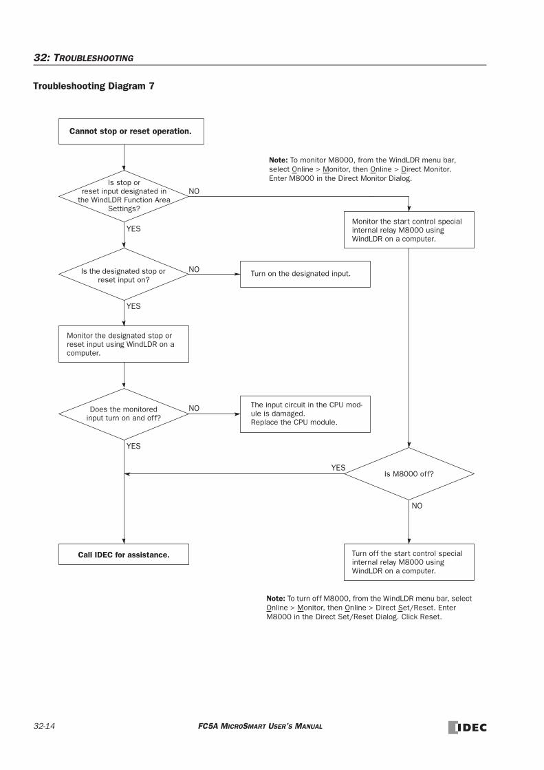
32: TROUBLESHOOTING
Troubleshooting Diagram 7
Does the monitored input turn on and off?
NO
YES
NO
YES
YES
Call IDEC for assistance.
Monitor the designated stop or reset input using WindLDR on a computer.
NOIs the designated stop or reset input on?
Is M8000 off?
Turn on the designated input.
The input circuit in the CPU mod-ule is damaged.Replace the CPU module.
Is stop or reset input designated in
the WindLDR Function Area Settings?
Monitor the start control special internal relay M8000 using WindLDR on a computer.
YES
Turn off the start control special internal relay M8000 using WindLDR on a computer.
NO
Cannot stop or reset operation.
Note: To monitor M8000, from the WindLDR menu bar, select Online > Monitor, then Online > Direct Monitor. Enter M8000 in the Direct Monitor Dialog.
Note: To turn off M8000, from the WindLDR menu bar, select Online > Monitor, then Online > Direct Set/Reset. Enter M8000 in the Direct Set/Reset Dialog. Click Reset.
32-14 FC5A MICROSMART USER’S MANUAL

32: TROUBLESHOOTING
Troubleshooting Diagram 8
Troubleshooting Diagram 9
YES
NO
Is the scan time longer than 340 ms?
NOP instruction can reset the watchdog timer. Insert NOP in the ladder diagram so that the watchdog timer does not exceed 340 ms.
Call IDEC for assistance.
Watchdog timer error occurs and the CPU does not run.
Are the input ON/OFF voltage levels correct?
Call IDEC for assistance.
The interrupt/catch input cannot receive short pulses.
END
YES
NO Make sure of correct input voltage. ON voltage: 15V DC minimumOFF voltage: 5V DC maximum
FC5A MICROSMART USER’S MANUAL 32-15

32: TROUBLESHOOTING
Troubleshooting Diagram 10
NO
YES
YES
NOAre the Function Area Settings completed?
Are input signals connected to correct
terminals?
Make sure that input signals are con-nected to correct terminals. See page 5-29.
Call IDEC for assistance.
Frequency measurement does not work.
Select Single-phase High-speed Counter in the Groups 1 through 4.
YES
NOIs the gate input on? Is the reset input off?
Make sure that the gate input is on and the reset input is off.
32-16 FC5A MICROSMART USER’S MANUAL
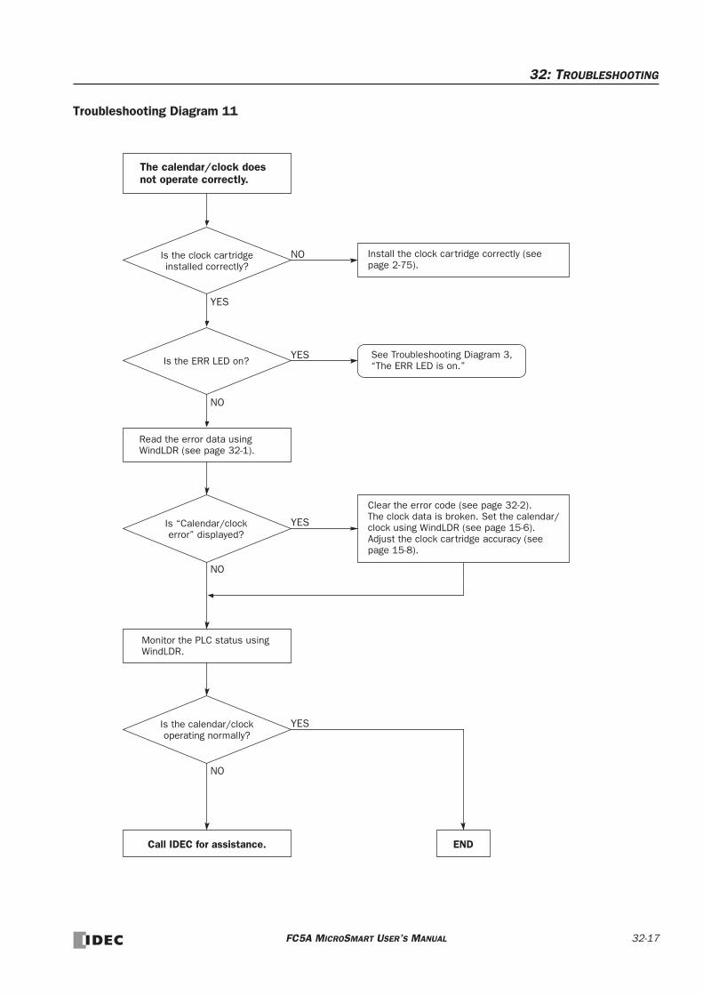
32: TROUBLESHOOTING
Troubleshooting Diagram 11
NO
Call IDEC for assistance.
YESIs the ERR LED on?
Is “Calendar/clock error” displayed?
YES
NO
The calendar/clock does not operate correctly.
See Troubleshooting Diagram 3,“The ERR LED is on.”
Read the error data using WindLDR (see page 32-1).
Is the calendar/clock operating normally?
Clear the error code (see page 32-2).The clock data is broken. Set the calendar/clock using WindLDR (see page 15-6). Adjust the clock cartridge accuracy (see page 15-8).
Monitor the PLC status using WindLDR.
YES
NO
END
YES
NOIs the clock cartridgeinstalled correctly?
Install the clock cartridge correctly (see page 2-75).
FC5A MICROSMART USER’S MANUAL 32-17

32: TROUBLESHOOTING
Troubleshooting Diagram 12
YES
NO
NO
YES
Does the status DR store status code 4
(hardware failure)?
Call IDEC for assistance.
Analog I/O module does not work (END refresh type).
Make sure of correct parameters.
YES
NOAfter changing settings, was the CPU stopped and
restarted?
Stop and restart the CPU to configure the analog I/O settings.
Supply the rated power voltage to the analog I/O module.
Does the status DR store status code 3
(invalid parameter)?
YES
NO
Are data registers duplicated?
Change data register numbers to eliminate duplicated data registers.
32-18 FC5A MICROSMART USER’S MANUAL

32: TROUBLESHOOTING
Troubleshooting Diagram 13
Turn off the power to the master station, and turn on the power after a few seconds.
Is the error code 0 at all stations?
Is thecommunication cable
connected to the RS485 port correctly?
Call IDEC for assistance.
NO
Make sure of correct wiring (see page 27-2).
END
Turn off M8006 using WindLDR.
Check error codes for the troubled stations (see page 27-4).
For the master station, click the Initialize Data Link button (see page 27-11) or turn on M8007 dur-ing operation using WindLDR.
Are error codes cleared to 0 at all
stations?
Clear the error codes at all stations using WindLDR (see page 32-2).
Data link communication is impossible.
NO
YES
YES
YES
NO
M8006: Data link communication prohibit flagM8007: Data link communication initialize flag
NO
YES
Is data link selected for port 2 correctly?
NO
YES
YES
NO
Is the PWR LED on? See Troubleshooting Diagram 1,“The PWR LED does not go on.”
Is M8006 on at the master station?
Check port 2 settings using WindLDR (see pages 27-7 and 27-8).
Select data link for port 2 correctly and down-load the user program again (see pages 27-7 and 27-8).
FC5A MICROSMART USER’S MANUAL 32-19
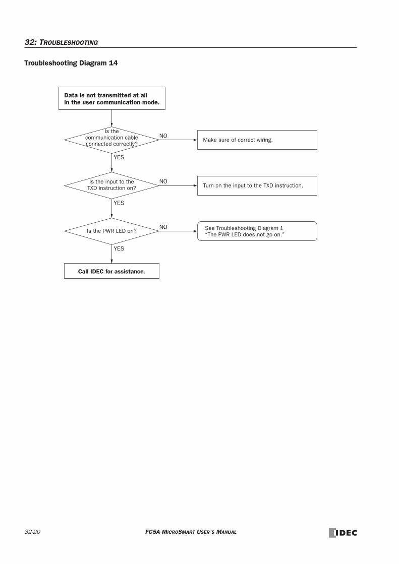
32: TROUBLESHOOTING
Troubleshooting Diagram 14
See Troubleshooting Diagram 1“The PWR LED does not go on.”
Is the PWR LED on?
Is thecommunication cableconnected correctly?
Call IDEC for assistance.
Make sure of correct wiring.
YES
YES
Is the input to the TXD instruction on? Turn on the input to the TXD instruction.
NO
NO
NO
YES
Data is not transmitted at all in the user communication mode.
32-20 FC5A MICROSMART USER’S MANUAL

32: TROUBLESHOOTING
Troubleshooting Diagram 15
Did you make sure of source 1 operand of the
TXD instruction?
Call IDEC for assistance.
NOAre communication parameters set correctly
using WindLDR?
NO
Are inputs to more than 5 TXD instructions on
simultaneously?
YES Correct the program to make sure that inputs to more than 5 TXD instructions do not go on simultaneously.
Data is not transmitted correctly in the user communication mode.
Set the communication parameters to match those of the remote terminal using WindLDR (see page 17-5).
Make sure that the busy signal at the remote terminal does not exceed 5 sec.
NO
NO
Is the data register designated as transmit status
used repeatedly?
Correct the program to replace the duplicate data register with a different data register.
Is duration of the busy signal at the remote
terminal less than 5 sec?
YES
NO
YES
Make sure that the transmit data desig-nated as source 1 operand is correct.
YES
YES
When the user communication still has a problem after completing the above procedure, also perform the procedure of Diagram 14 described on the preceding page.
FC5A MICROSMART USER’S MANUAL 32-21

32: TROUBLESHOOTING
Troubleshooting Diagram 16
See Troubleshooting Diagram 1“The PWR LED does not go on.”
Is the PWR LED on?
Is thecommunication cableconnected correctly?
Call IDEC for assistance.
Make sure of correct wiring.
YES
YES
Is the input to the RXD instruction on? Turn on the input to the RXD instruction.
NO
NO
NO
YES
Data is not received at all in the user communication mode.
32-22 FC5A MICROSMART USER’S MANUAL

32: TROUBLESHOOTING
Troubleshooting Diagram 17
Did you make sure of source 1 operand of the
RXD instruction?
Call IDEC for assistance.
NOAre communication parameters set correctly
using WindLDR?
Are inputs to more than 5 RXD instructions on
simultaneously?
Data is not received correctly in the user communication mode.
Set the communication parameters to match those of the remote termi-nal using WindLDR. MicroSmart can use constants only for start and stop delimiters (see page 17-5.)
Is the data register designated as receive status
used repeatedly?
Correct the program to replace the duplicate data register with a differ-ent data register.
YES
NO
Is a start delimiter specified in the RXD
instruction?
YES
Did you check the start delimiter of incoming
data?
Did you check the format of incoming
data?
Is an end delimiter specified in the RXD
instruction?
Did you check the end delimiter of
incoming data?
Is the receive timeout value set correctly
using WindLDR?
Is one input used to start multiple RXD
instructions?
Make sure that the receive format of the RXD instruction matches that of the incoming data.
Correct the program to make sure that inputs to more than 5 RXD instructions do not go on simultaneously.
NO
YES
NO
YES
YES
YES
YES
YES
YES
NO
YES
NO
Use one input to start one RXD instruction without a start delim-iter.
Make sure that the start delimiter in the RXD instruction matches that of the incoming data.
Make sure that the end delimiter in the RXD instruction matches that of the incoming data.
Make sure that the receive timeout value is larger than character inter-vals of the incoming data.
Make sure that the receive data designated as the source 1 oper-and is correct.
YES
NO
NO
NO
NO
NO
FC5A MICROSMART USER’S MANUAL 32-23

32: TROUBLESHOOTING
Troubleshooting Diagram 18
Confirm slave settings again.
Make sure that the slave is compat-ible with the function code.
Make sure that the slave number and communication settings are correct.
Are communication parameters equal at master
and slave?
Modbus master communication does not work.
Are error data stored in D8069 to D8099?
YES
NO
Is request execution IR designated and
turned on?
YES
NO
NO
Confirm communication settings using WindLDR (see page 30-4).
Confirm the slave number (high-order byte) and error code (low-order byte) (see page 30-7).
Make sure that slave address set-tings are correct.
Turn on the request execution internal relay.
YES
Is it clear which request has an error?
NO
See the request table to find which request has an error and what error occurred (see page 30-3).
YES01h (function error)?
NO
02h (access destination error)?
NO
YES03h (operand quantity error, 1-bit write
data error)?
NO
YES16h (timeout error)?
NO
YES
Make sure of the valid slave address range and master settings.
YES
Data size and actual data may not match. Make sure that slave set-tings and hardware are correct (without noise and failure).
32-24 FC5A MICROSMART USER’S MANUAL

32: TROUBLESHOOTING
Troubleshooting Diagram 19
Modbus master communication request is slow.
END
Select to use request execution internal relay and designate an inter-nal relay number.
Keep unnecessary internal relays turned off and turn on internal relays only when sending requests.
FC5A MICROSMART USER’S MANUAL 32-25

32: TROUBLESHOOTING
32-26 FC5A MICROSMART USER’S MANUAL
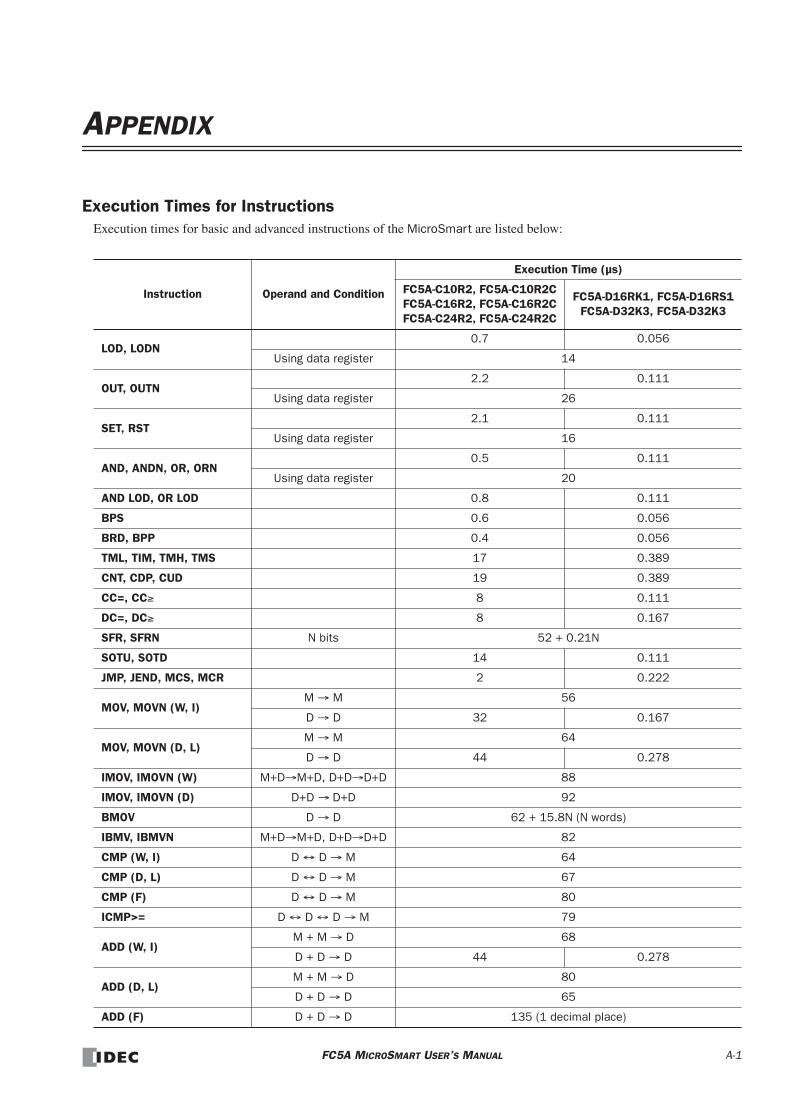
APPENDIX
Execution Times for InstructionsExecution times for basic and advanced instructions of the MicroSmart are listed below:
Instruction Operand and Condition
Execution Time (µs)
FC5A-C10R2, FC5A-C10R2CFC5A-C16R2, FC5A-C16R2CFC5A-C24R2, FC5A-C24R2C
FC5A-D16RK1, FC5A-D16RS1FC5A-D32K3, FC5A-D32K3
LOD, LODN0.7 0.056
Using data register 14
OUT, OUTN2.2 0.111
Using data register 26
SET, RST2.1 0.111
Using data register 16
AND, ANDN, OR, ORN0.5 0.111
Using data register 20
AND LOD, OR LOD 0.8 0.111
BPS 0.6 0.056
BRD, BPP 0.4 0.056
TML, TIM, TMH, TMS 17 0.389
CNT, CDP, CUD 19 0.389
CC=, CC≥ 8 0.111
DC=, DC≥ 8 0.167
SFR, SFRN N bits 52 + 0.21N
SOTU, SOTD 14 0.111
JMP, JEND, MCS, MCR 2 0.222
MOV, MOVN (W, I)M → M 56
D → D 32 0.167
MOV, MOVN (D, L)M → M 64
D → D 44 0.278
IMOV, IMOVN (W) M+D→M+D, D+D→D+D 88
IMOV, IMOVN (D) D+D → D+D 92
BMOV D → D 62 + 15.8N (N words)
IBMV, IBMVN M+D→M+D, D+D→D+D 82
CMP (W, I) D ↔ D → M 64
CMP (D, L) D ↔ D → M 67
CMP (F) D ↔ D → M 80
ICMP>= D ↔ D ↔ D → M 79
ADD (W, I)M + M → D 68
D + D → D 44 0.278
ADD (D, L)M + M → D 80
D + D → D 65
ADD (F) D + D → D 135 (1 decimal place)
FC5A MICROSMART USER’S MANUAL A-1

APPENDIX
SUB (W, I)M – M → D 71
D – D → D 60 0.278
SUB (D, L)M – M → D 91
D – D → D 66
SUB (F) D – D → D 134 (1 decimal place)
MUL (W, I)M × M → D 61
D × D → D 60
MUL (D, L)M × M → D 83
D × D → D 76
MUL (F) D × D → D 104
DIV (W, I)M ÷ M → D 71
D ÷ D → D 71
DIV (D, L)M ÷ M → D 98
D ÷ D → D 89
DIV (F) D ÷ D → D 166
ROOT (W) 165
ROOT (D) 228
ROOT (F) 926
ANDW, ORW, XORW (W) M · M → D, D · D → D 60
ANDW, ORW, XORW (D) D · D → D 65
SFTL, SFTR N_B = 100 125
BCDLS D → D, S1 = 1 77
WSFT D → D 62 + 16.1N (N words to shift)
ROTL, ROTR D, bits = 1 46
HTOB D → D 61
BTOH D → D 56
HTOA D → D 66
ATOH D → D 62
BTOA D → D 68
ATOB D → D 61
ENCO M → D, 16 bits 42
DECO D → M 47
BCNT M → D, 16 bits 185
ALT 33
CVNTW, I, D, L → F 106
F → W, I, D, L 142
DISPBCD 5 digits 70
BIN 4 digits 66
DGRDBCD 5 digits 62
BIN 4 digits 61
LCAL 32
LRET 17
Instruction Operand and Condition
Execution Time (µs)
FC5A-C10R2, FC5A-C10R2CFC5A-C16R2, FC5A-C16R2CFC5A-C24R2, FC5A-C24R2C
FC5A-D16RK1, FC5A-D16RS1FC5A-D32K3, FC5A-D32K3
D → D
D → D
D → D
A-2 FC5A MICROSMART USER’S MANUAL

APPENDIX
Note: Repeat is not designated for any operand.
Processing in One ScanWhile the MicroSmart CPU module is running, the CPU module performs operations repeatedly such as input refreshing, ladder program processing, output refreshing, and error checking.
A scan is the execution of all instructions from address zero to the END instruction. The time required for this execution is referred to as one scan time. The scan time varies with respect to program length.
The current value of the scan time is stored to special data register D8023 (scan time current value), and the maximum value of the scan time is stored to special data register D8024 (scan time maximum value). These values can be viewed on the PLC status screen of WindLDR while monitoring on a PC.
Executing Program InstructionsDuring the scan time, program instructions are processed sequentially starting with the first line of the ladder program, except for interrupt program execution. The one scan time of a ladder program is approximately equal to the total of exe-cution time of each instruction shown on preceding pages.
Watchdog TimerThe watchdog timer monitors the time required for one program cycle (scan time) to prevent hardware malfunction. When the time exceeds approximately 340 ms, the watchdog timer indicates an error and stops CPU operation. If this is the case, place NOP instructions in the ladder diagram. The NOP instruction resets the watchdog timer.
IOREF 18
HSCRF 36
FRQRF 33
EI 25
DI 22
AVRG (W, I) S3 = 10 84
AVRG (D, L) S3 = 10 88
AVRG (F) S3 = 10 161
PID AT+PID in progress 520
DTML, DTIM, DTMH 87
DTMS 92
TTIM 50
RAD F → F 127
DEG F → F 145
SIN, COS F → F 1826
TAN F → F 1736
ASIN, ACOS F → F 6090
ATAN F → F 5402
LOGE, LOG10 F → F 2999
EXP F → F 1072
POW F → F 3819
Instruction Operand and Condition
Execution Time (µs)
FC5A-C10R2, FC5A-C10R2CFC5A-C16R2, FC5A-C16R2CFC5A-C24R2, FC5A-C24R2C
FC5A-D16RK1, FC5A-D16RS1FC5A-D32K3, FC5A-D32K3
FC5A MICROSMART USER’S MANUAL A-3

APPENDIX
Breakdown of END Processing TimeThe END processing time depends on the MicroSmart settings and system configuration. The total of execution times for applicable conditions shown below is the actual END processing time.
Note 1: Expansion bus processing time per ladder refresh type analog I/O module depends on the byte count of the RUNA/STPA communication data.Note 2: Processing time of AS-Interface master module 2 depends on the byte count of the RUNA/STPA communication data.Note 3: Clock function is processed once every 500 ms.
I/O Refreshing by Expansion Interface ModuleThe expansion interface module performs I/O refreshing independent of the I/O refreshing by the CPU module. While the I/O refresh time (D8252 expansion interface module I/O refresh time ×100 µs) of the expansion interface module is longer than the CPU module scan time (D8023 scan time current value in ms), executing OUT/OUTN, SET/RST, SOTU/SOTD or ALT instructions, which change output statuses every scan, may fail to generate outputs to the output modules beyond the expansion interface module correctly in every scan.
If the I/O refresh time of the expansion interface module is longer than the CPU module scan time, adjust the scan time using special data register D8022 (constant scan time preset value in ms) or change the mounting positions of the expan-sion I/O modules.
Item Condition Execution Time
Housekeeping (built-in I/O service) Slim 32-I/O type CPU 263 µs
Expansion I/O service(1 expansion I/O module)
8 inputs or 8 outputs 130 µs
16 inputs or 16 outputs 183 µs
32 inputs or 32 outputs 357 µs
4 inputs and 4 outputs 127 µs
16 inputs and 8 outputs 305 µs
Expansion Processing(1 analog I/O module) (Note 1)
END refresh type 1.8 ms
Expansion Processing(1 expansion interface module)
Integrated or separate mounting2.5 ms (one 4-in/4-out mixed I/O module) 4.5 ms (seven 32-I/O modules)
AS-Interface Master Module (Note 2) AS-Interface master module 1 9.4 ms
Clock function processing (Note 3) 850 µs
A-4 FC5A MICROSMART USER’S MANUAL

APPENDIX
Instruction Steps and Applicability in Interrupt ProgramsThe steps and bytes of basic and advanced instructions are listed below. Applicability of basic and advanced instructions in interrupt programs are also shown in the rightmost column of the following tables.
Note: One bit of data register is not used in the measurement of steps and bytes of basic instructions.
Basic InstructionAll-in-One Type CPU Module Slim Type CPU Module
InterruptQty of Steps Qty of Bytes Qty of Steps Qty of Bytes
LOD, LODN 1.00 6 0.67 4 X
OUT, OUTN 1.00 6 0.67 4 X
SET, RST 1.00 6 0.67 4 X
AND, ANDN, OR, ORN 1.00 6 0.67 4 X
AND LOD, OR LOD 0.83 5 0.67 4 X
BPS 0.83 5 0.67 4 X
BRD 0.50 3 0.67 4 X
BPP 0.33 2 0.67 4 X
TML, TIM, TMH, TMS 0.67 4 2.00 12 —
CNT, CDP, CUD 0.67 4 2.00 12 —
CC=, CC≥ 1.17 7 1.67 10 X
DC=, DC≥ 1.33 8 1.67 10 X
SFR, SFRN 1.00 6 1.67 10 —
SOTU, SOTD 0.83 5 0.67 4 —
JMP 1.00 4 1.00 6 X
JEND, MCS, MCR 0.67 4 0.67 4 X
END 0.33 2 0.67 4 X
Advanced InstructionAll-in-One Type CPU Module Slim Type CPU Module
InterruptQty of Steps Qty of Bytes Qty of Steps Qty of Bytes
NOP 0.33 2 0.67 4 X
MOV, MOVN 2.67 to 3.00 16 to 18 2.00 to 2.67 12 to 16 X
IMOV, IMOVN 3.33 to 4.00 20 to 24 2.33 to 2.67 14 to 16 X
BMOV 3.00 18 2.00 to 2.67 12 to 16 X
IBMV, IBMVN 3.33 to 4.00 20 to 24 2.33 to 2.67 14 to 16 X
CMP 3.33 to 4.00 20 to 24 2.33 to 3.67 14 to 22 X
ICMP>= 3.67 to 4.67 22 to 28 2.33 to 4.33 14 to 26 X
ADD, SUB, MUL, DIV 3.33 to 4.00 20 to 24 2.33 to 3.67 14 to 22 X
ROOT 2.33 to 2.67 14 to 16 1.67 to 2.33 10 to 14 X
ANDW, ORW, XORW 3.33 to 4.00 20 to 24 2.33 to 3.67 14 to 22 X
SFTL, SFTR 3.67 22 2.33 to 3.33 14 to 20 X
BCDLS 2.33 14 1.67 to 2.00 10 to 12 X
WSFT 3.00 18 2.00 to 2.67 12 to 16 X
ROTL, ROTR 2.00 12 1.67 10 X
HTOB, BTOH 2.33 to 2.67 14 to 16 1.67 to 2.33 10 to 14 X
HTOA, ATOH, BTOA, ATOB 3.00 to 3.67 18 to 22 2.00 to 2.67 12 to 16 X
ENCO, DECO 2.67 16 2.00 to 2.33 12 to 14 X
BCNT 3.00 18 2.00 to 2.33 12 to 14 X
ALT 1.67 10 1.33 8 X
FC5A MICROSMART USER’S MANUAL A-5

APPENDIX
CVDT 2.67 to 3.00 16 to 18 2.00 to 2.67 12 to 16 X
WKTIM 4.00 24 2.67 to 3.67 16 to 22 —
WKTBL 2.00 to 14.67 12 to 88 1.67 to 14.67 10 to 88 —
DISP 2.67 16 2.00 12 —
DGRD 3.33 20 2.33 14 —
TXD1, TXD2, RXD1, RXD2 3.50 to 136.50 21 to 819 2.67 to 135.67 16 to 814 —
LABEL 1.33 8 1.33 8 X
LJMP, LCAL 1.67 10 1.33 to 1.67 8 to 10 X
LRET 1.00 6 1.00 6 X
IOREF 2.00 12 1.67 10 X
HSCRF, FRQRF 1.00 6 1.00 6 X
DI, EI 1.33 8 1.33 8 —
XYFS 4.67 to 44.67 28 to 268 3.33 to 44.67 20 to 268 —
CVXTY, CVYTX 3.00 18 2.33 to 2.67 14 to 16 —
AVRG 4.33 26 2.67 to 3.00 16 to 18 —
PULS1, PULS2, PULS3 — — 1.67 10 —
PWM1, PWM2, PWM3 — — 1.67 10 —
RAMP1, RAMP2 — — 1.67 10 —
ZRN1, ZRN2, ZRN3 — — 2.00 12 —
PID 4.33 26 2.67 to 3.00 16 to 18 —
DTML, DTIM, DTMH, DTMS 3.67 22 2.33 to 3.00 14 to 18 —
TTIM 1.67 10 1.33 8 —
RUNA, STPA 3.33 20 2.67 to 3.00 16 to 18 —
RAD, DEG, SIN, COS, TAN, ASIN, ACOS, ATAN
2.33 to 2.67 14 to 16 1.67 to 2.33 10 to 14 X
LOGE, LOG10, EXP 2.33 to 2.67 14 to 16 1.67 to 2.33 10 to 14 X
POW 3.00 to 3.67 18 to 22 2.00 to 3.33 12 to 20 X
Advanced InstructionAll-in-One Type CPU Module Slim Type CPU Module
InterruptQty of Steps Qty of Bytes Qty of Steps Qty of Bytes
A-6 FC5A MICROSMART USER’S MANUAL

APPENDIX
CablesCommunication cables and their connector pinouts are described in this section.
Communication Port and Applicable Cables
Modem Cable 1C (FC2A-KM1C)
Cable Length: 3m (9.84 feet)
Connector Communication Port Applicable Cable
RS232C Mini DIN Connector
Built-in port on CPU module FC2A-KM1CFC2A-KC4CFC2A-KP1CFC4A-KC1CFC4A-KC2C
FC4A-PC1 (RS232C Communication Adapter)
FC4A-HPC1 (RS232C Communication Module)
FC4A-SX5ES1E (Web Server Unit) FC4A-KC3C
RS485 Mini DIN ConnectorFC4A-PC2 (RS485 Communication Adapter)
FC2A-KP1CFC4A-HPC2 (RS485 Communication Module)
To MicroSmart Port 2
D-sub 25-pin Male Connector Pinouts
Pin Description1 FG Frame Ground2 TXD Transmit Data3 RXD Receive Data4 RTS Request to Send5 NC No Connection6 NC No Connection7 SG Signal Ground8 DCD Data Carrier Detect20 DTR Data Terminal Ready
Mini DIN Connector Pinouts
Description PinShield CoverRTS Request to Send 1DTR Data Terminal Ready 2TXD Transmit Data 3RXD Receive Data 4DSR Data Set Ready 5SG Signal Ground 6SG Signal Ground 7NC No Connection 8
To Modem RS232C Port
FC5A MICROSMART USER’S MANUAL A-7

APPENDIX
Computer Link Cable 4C (FC2A-KC4C)
Cable Length: 3m (9.84 feet)
User Communication Cable 1C (FC2A-KP1C)
Cable Length: 2.4m (7.87 feet)
To MicroSmart RS232C Port 1 or 2
D-sub 9-pin Female Connector Pinouts
Pin DescriptionCover FG Frame Ground
3 TXD Transmit Data2 RXD Receive Data6 DSR Data Set Ready8 CTS Clear to Send1 DCD Data Carrier Detect4 DTR Data Terminal Ready5 SG Signal Ground7 RTS Request to Send9 RI Ring Indicator
Mini DIN Connector Pinouts
Description PinShield CoverTXD Transmit Data 3RXD Receive Data 4RTS Request to Send 1NC No Connection 8DSR Data Set Ready 5DTR Data Terminal Ready 2SG Signal Ground 7SG Signal Ground 6
To Computer RS232C Port
To MicroSmart RS232C Port 1 or 2 To RS232C Port
Attach a proper connector to the open end referring to the cable connector pinouts shown below.
Mini DIN Connector Pinouts
Note: When preparing a cable for port 1, keep pins 6 and 7 open. If pins 6 and 7 are connected together, user com-munication cannot be used. Make sure that unused leads do not interconnect.
Pin Port 1 Port 2 AWG# Color1 NC No Connection RTS Request to Send 28
TwistedBlack
2 NC No Connection DTR Data Terminal Ready 28 Yellow3 TXD Transmit Data TXD Transmit Data 28 Blue4 RXD Receive Data RXD Receive Data 28 Green5 NC No Connection DSR Data Set Ready 28 Brown6 CMSW Communication Switch SG Signal Ground 28 Gray7 SG Signal Ground SG Signal Ground 26
TwistedRed
8 NC No Connection NC No Connection 26 WhiteCover — — — Shield
• Do not connect any wiring to NC terminals, otherwise operation failure or device damage may be caused.
Caution
Signal Direction
1
2
3
4
5
6
7
8
A-8 FC5A MICROSMART USER’S MANUAL
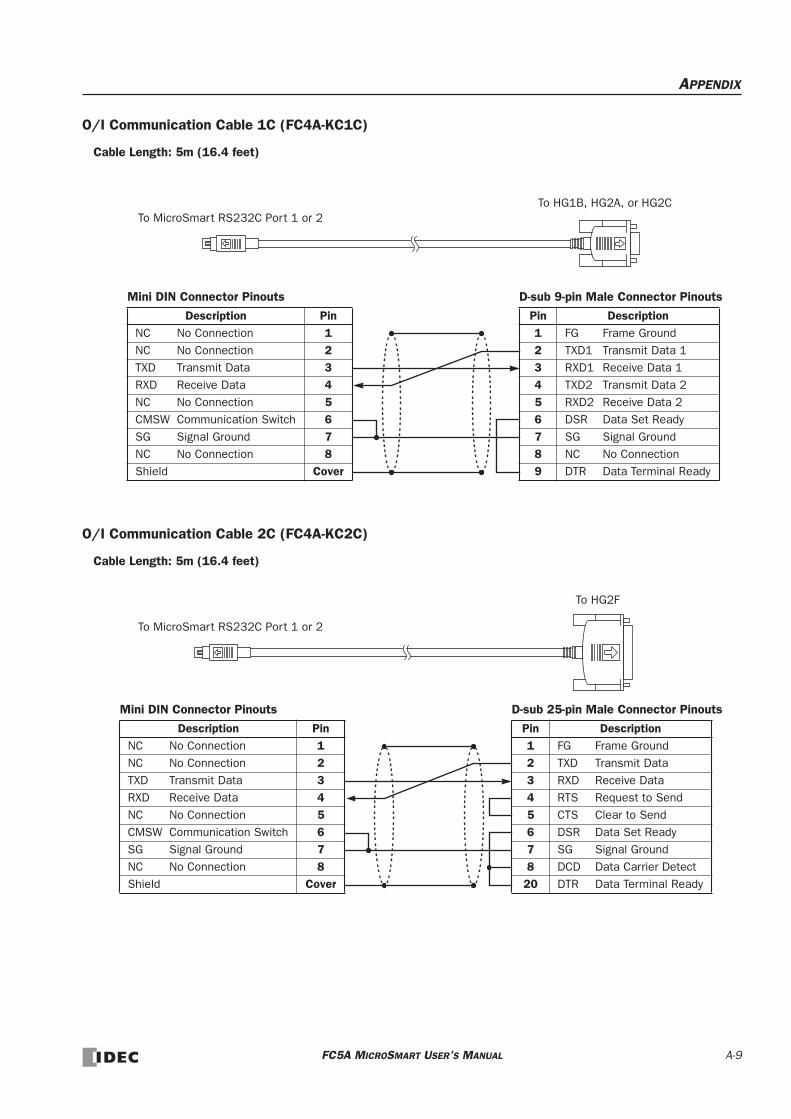
APPENDIX
O/I Communication Cable 1C (FC4A-KC1C)
Cable Length: 5m (16.4 feet)
O/I Communication Cable 2C (FC4A-KC2C)
Cable Length: 5m (16.4 feet)
Mini DIN Connector Pinouts
Description PinNC No Connection 1NC No Connection 2TXD Transmit Data 3RXD Receive Data 4NC No Connection 5CMSW Communication Switch 6SG Signal Ground 7NC No Connection 8Shield Cover
To MicroSmart RS232C Port 1 or 2To HG1B, HG2A, or HG2C
D-sub 9-pin Male Connector Pinouts
Pin Description1 FG Frame Ground2 TXD1 Transmit Data 13 RXD1 Receive Data 14 TXD2 Transmit Data 25 RXD2 Receive Data 26 DSR Data Set Ready7 SG Signal Ground8 NC No Connection9 DTR Data Terminal Ready
Mini DIN Connector Pinouts
Description PinNC No Connection 1NC No Connection 2TXD Transmit Data 3RXD Receive Data 4NC No Connection 5CMSW Communication Switch 6SG Signal Ground 7NC No Connection 8Shield Cover
To MicroSmart RS232C Port 1 or 2
D-sub 25-pin Male Connector Pinouts
Pin Description1 FG Frame Ground2 TXD Transmit Data3 RXD Receive Data4 RTS Request to Send5 CTS Clear to Send6 DSR Data Set Ready7 SG Signal Ground8 DCD Data Carrier Detect
20 DTR Data Terminal Ready
To HG2F
FC5A MICROSMART USER’S MANUAL A-9
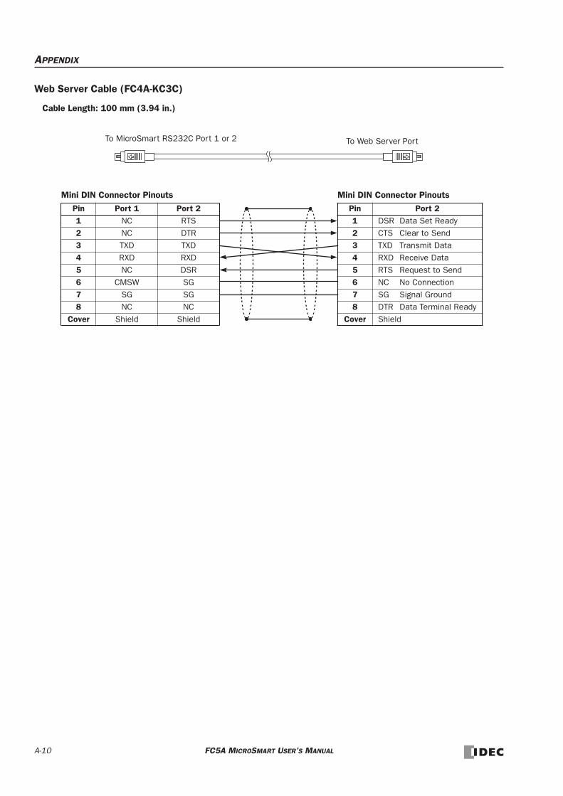
APPENDIX
Web Server Cable (FC4A-KC3C)
Cable Length: 100 mm (3.94 in.)
To MicroSmart RS232C Port 1 or 2 To Web Server Port
Mini DIN Connector Pinouts
Pin Port 1 Port 21 NC RTS2 NC DTR3 TXD TXD4 RXD RXD5 NC DSR6 CMSW SG7 SG SG8 NC NC
Cover Shield Shield
Mini DIN Connector Pinouts
Pin Port 21 DSR Data Set Ready2 CTS Clear to Send3 TXD Transmit Data4 RXD Receive Data5 RTS Request to Send6 NC No Connection7 SG Signal Ground8 DTR Data Terminal Ready
Cover Shield
A-10 FC5A MICROSMART USER’S MANUAL
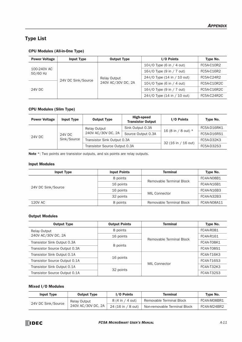
APPENDIX
Type List
CPU Modules (All-in-One Type)
CPU Modules (Slim Type)
Note *: Two points are transistor outputs, and six points are relay outputs.
Input Modules
Output Modules
Mixed I/O Modules
Power Voltage Input Type Output Type I/O Points Type No.
100-240V AC50/60 Hz
24V DC Sink/SourceRelay Output 240V AC/30V DC, 2A
10-I/O Type (6 in / 4 out) FC5A-C10R2
16-I/O Type (9 in / 7 out) FC5A-C16R2
24-I/O Type (14 in / 10 out) FC5A-C24R2
24V DC
10-I/O Type (6 in / 4 out) FC5A-C10R2C
16-I/O Type (9 in / 7 out) FC5A-C16R2C
24-I/O Type (14 in / 10 out) FC5A-C24R2C
Power Voltage Input Type Output TypeHigh-speed
Transistor OutputI/O Points Type No.
24V DC24V DC Sink/Source
Relay Output 240V AC/30V DC, 2A
Sink Output 0.3A16 (8 in / 8 out) *
FC5A-D16RK1
Source Output 0.3A FC5A-D16RS1
Transistor Sink Output 0.3A32 (16 in / 16 out)
FC5A-D32K3
Transistor Source Output 0.3A FC5A-D32S3
Input Type Input Points Terminal Type No.
24V DC Sink/Source
8 pointsRemovable Terminal Block
FC4A-N08B1
16 points FC4A-N16B1
16 pointsMIL Connector
FC4A-N16B3
32 points FC4A-N32B3
120V AC 8 points Removable Terminal Block FC4A-N08A11
Output Type Output Points Terminal Type No.
Relay Output240V AC/30V DC, 2A
8 points
Removable Terminal Block
FC4A-R081
16 points FC4A-R161
Transistor Sink Output 0.3A8 points
FC4A-T08K1
Transistor Source Output 0.3A FC4A-T08S1
Transistor Sink Output 0.1A16 points
MIL Connector
FC4A-T16K3
Transistor Source Output 0.1A FC4A-T16S3
Transistor Sink Output 0.1A32 points
FC4A-T32K3
Transistor Source Output 0.1A FC4A-T32S3
Input Type Output Type I/O Points Terminal Type No.
24V DC Sink/SourceRelay Output240V AC/30V DC, 2A
8 (4 in / 4 out) Removable Terminal Block FC4A-M08BR1
24 (16 in / 8 out) Non-removable Terminal Block FC4A-M24BR2
FC5A MICROSMART USER’S MANUAL A-11

APPENDIX
Analog I/O Modules
Web Server Unit
AS-Interface Master Module
Optional Modules, Adapters, and Cartridges
Note *: RS232C or RS485 communication adapters can also be installed on the HMI base module mounted next to the slim type CPU module.
Name I/O Signal I/O Points Category Terminal Type No.
Analog I/O Module
Voltage (0 to 10V DC) Current (4 to 20mA) 2 inputs
END Refresh Type
Removable Terminal Block
FC4A-L03A1Voltage (0 to 10V DC) Current (4 to 20mA) 1 output
Thermocouple (K, J, T) Resistance thermometer (Pt100) 2 inputs
FC4A-L03AP1Voltage (0 to 10V DC) Current (4 to 20mA) 1 output
Analog Input Module
Voltage (0 to 10V DC) Current (4 to 20mA) 2 inputs FC4A-J2A1
Voltage (0 to 10V DC) Current (4 to 20mA) Thermocouple (K, J, T) Resistance thermometer (Pt100, Pt1000, Ni100, Ni1000)
4 inputsLadder Refresh Type
FC4A-J4CN1
Voltage (0 to 10V DC) Current (4 to 20mA) 8 inputs FC4A-J8C1
Thermistor (PTC, NTC) 8 inputs FC4A-J8AT1
Analog Output Module
Voltage (0 to 10V DC) Current (4 to 20mA) 1 output END
Refresh FC4A-K1A1
Voltage (–10 to +10V DC) Current (4 to 20mA) 2 outputs Ladder
Refresh FC4A-K2C1
Name Terminal Type No.
Web Server Unit Screw Terminal FC4A-SX5ES1E
Name Terminal Type No.
AS-Interface Master Module Removable Terminal Block FC4A-AS62M
Name Description Type No.
Expansion Interface Module For integrated mounting FC5A-EXM2
Expansion Interface Master ModuleFor separate mounting
FC5A-EXM1M
Expansion Interface Slave Module FC5A-EXM1S
HMI Module For displaying and changing required operands FC4A-PH1
HMI Base Module For mounting HMI module with slim type CPU module FC4A-HPH1
RS232C Communication Adapter * Mini DIN connector type for all-in-one 16- and 24-I/O CPU modules FC4A-PC1
RS485 Communication Adapter *Mini DIN connector type for all-in-one 16- and 24-I/O CPU modules FC4A-PC2
Terminal block type for all-in-one 16- and 24-I/O CPU modules FC4A-PC3
RS232C Communication Module Mini DIN connector type for slim type CPU module FC4A-HPC1
RS485 Communication ModuleMini DIN connector type for slim type CPU module FC4A-HPC2
Terminal block type for slim type CPU module FC4A-HPC3
Memory Cartridge32KB EEPROM for storing a user program FC4A-PM32
64KB EEPROM for storing a user program FC4A-PM64
Clock Cartridge Real time calendar/clock function FC4A-PT1
A-12 FC5A MICROSMART USER’S MANUAL

APPENDIX
Accessories
BX Series I/O Terminals and Applicable Cables
Specify required designation codes in place of ➀, ➁, and ➂.
Name Function Type No.
RS232C/RS485 ConverterUsed for interface between a computer and the MicroSmart CPU modules in the computer link 1:N communication system or through modems
FC2A-MD1
RS232C Cable (4-wire) (1.5m/4.92 ft. long)
Used to connect the RS232C/RS485 converter to a computer, with D-sub 9-pin female connector to connect to computer
HD9Z-C52
DIN Rails(1m/3.28 ft. long)
35-mm-wide aluminum DIN rail to mount MicroSmart modules (package quantity 10)
BAA1000NP10
DIN Rails(1m/3.28 ft. long)
35-mm-wide steel DIN rail to mount MicroSmart modules (package quantity 10)
BAP1000NP10
Mounting ClipsUsed on DIN rail to fasten MicroSmart modules (package quantity 10)
BNL6P
Direct Mounting StripsUsed for direct mounting of slim type CPU or I/O modules on a panel (package quantity 5)
FC4A-PSP1P
10-position Terminal Blocks For I/O modules (package quantity 2) FC4A-PMT10P
11-position Terminal Blocks For I/O modules (package quantity 2) FC4A-PMT11P
13-position Terminal BlocksFor slim type CPU modules FC4A-D20RK1 and FC4A-D20RS1 (package quantity 2)
FC4A-PMT13P
16-position Terminal Blocks For slim type CPU module FC5A-D16RK1 (package quantity 2) FC4A-PMTK16P
16-position Terminal Blocks For slim type CPU module FC5A-D16RS1 (package quantity 2) FC4A-PMTS16P
20-position Connector Socket MIL connector for I/O modules (package quantity 2) FC4A-PMC20P
26-position Connector Socket MIL connector for slim type CPU modules (package quantity 2) FC4A-PMC26P
Phoenix Ferrule Ferrule for connecting 1 or 2 wires to screw terminal See page 3-19
Phoenix Crimping Tool Used for crimping ferrules See page 3-19
Phoenix Screwdriver Used for tightening screw terminals See page 3-19
WindLDR Programming and monitoring software for Windows PC (CD) FC9Y-LP2CDW
MicroSmart User’s Manual This printed manual FC9Y-B927
Web Server Unit User’s Manual Printed manual for the web server unit FC9Y-B919
MicroSmartCable Type No. I/O Terminal Type No. Connector
Module Type No.
CPU ModuleFC5A-D32K3 FC5A-D32S3
FC9Z-H➀➁26BX1D-➂26A BX1F-➂26A
26-pole MIL connector
Input ModuleFC4A-N16B3 FC4A-N32B3
FC9Z-H➀➁20BX1D-➂20A BX1F-➂20A BX7D-BT16A1T (16-pt relay output)
20-pole MIL connectorOutput Module
FC4A-T16K3 FC4A-T16S3 FC4A-T32K3 FC4A-T32S3
➀ Cable Length Code ➁ Cable Shield Code ➂ Terminal Screw Style Code
050: 0.5m100: 1m200: 2m300: 3m
A: Shielded cableB: Non-shielded cable
T: Touch-down terminalS: Screw terminal
FC5A MICROSMART USER’S MANUAL A-13

APPENDIX
Cables
Name Function Type No.
Modem Cable 1C (3m/9.84 ft. long)
Used to connect a modem to the MicroSmart RS232C port, with D-sub 25-pin male connector to connect to modem
FC2A-KM1C
Computer Link Cable 4C (3m/9.84 ft. long)
Used to connect a computer to the MicroSmart RS232C port (1:1 computer link), with D-sub 9-pin female connector to connect to computer
FC2A-KC4C
User Communication Cable 1C (2.4m/7.87 ft. long)
Used to connect RS232C equipment to the MicroSmart RS232C port, without a connector to connect to RS232C equipment
FC2A-KP1C
O/I Communication Cable 1C (5m/16.4 ft. long)
RS232C cable used to connect IDEC HG1B/2A/2C operator inter-face to MicroSmart RS232C port 1 or 2
FC4A-KC1C
O/I Communication Cable 2C (5m/16.4 ft. long)
RS232C cable used to connect IDEC HG2F operator interface to MicroSmart RS232C port 1 or 2
FC4A-KC2C
Analog Voltage Input Cable (1m/3.28 ft. long)
Used to connect an analog voltage source to the analog voltage input connector on the slim type CPU module (package quantity 2)
FC4A-PMAC2P
Web Server Cable (100 mm/3.94 in.)
Used to connect the web server unit to MicroSmart RS232C port 1 or 2
FC4A-KC3C
Expansion Interface Cable (1m/3.28 ft. long)
Used to connect separate mounting type expansion interface mas-ter and slave modules
FC5A-KX1C
Shielded CPU Flat Cable (0.5m/1.64 ft. long)
26-wire shielded straight cable for connecting the MicroSmart slim type CPU module to an I/O terminal
FC9Z-H050A26
Shielded CPU Flat Cable (1m/3.28 ft. long)
FC9Z-H100A26
Shielded CPU Flat Cable (2m/6.56 ft. long)
FC9Z-H200A26
Shielded CPU Flat Cable (3m/9.84 ft. long)
FC9Z-H300A26
Non-shielded CPU Flat Cable (0.5m/1.64 ft. long)
26-wire non-shielded straight cable for connecting the MicroSmart slim type CPU module to an I/O terminal
FC9Z-H050B26
Non-shielded CPU Flat Cable (1m/3.28 ft. long)
FC9Z-H100B26
Non-shielded CPU Flat Cable (2m/6.56 ft. long)
FC9Z-H200B26
Non-shielded CPU Flat Cable (3m/9.84 ft. long)
FC9Z-H300B26
Shielded I/O Flat Cable (0.5m/1.64 ft. long)
20-wire shielded straight cable for connecting the MicroSmart I/O module to an I/O terminal
FC9Z-H050A20
Shielded I/O Flat Cable (1m/3.28 ft. long)
FC9Z-H100A20
Shielded I/O Flat Cable (2m/6.56 ft. long)
FC9Z-H200A20
Shielded I/O Flat Cable (3m/9.84 ft. long)
FC9Z-H300A20
Non-shielded I/O Flat Cable (0.5m/1.64 ft. long)
20-wire non-shielded straight cable for connecting the MicroSmart I/O module to an I/O terminal
FC9Z-H050B20
Non-shielded I/O Flat Cable (1m/3.28 ft. long)
FC9Z-H100B20
Non-shielded I/O Flat Cable (2m/6.56 ft. long)
FC9Z-H200B20
Non-shielded I/O Flat Cable (3m/9.84 ft. long)
FC9Z-H300B20
A-14 FC5A MICROSMART USER’S MANUAL

INDEX
# 1:1 computer link 4-11:N computer link 28-1100-ms
clock M8122 6-13dual timer 22-1
10-msclock M8123 6-13dual timer 22-1
1-ms dual timer 22-11-sec
clockM8121 6-13reset M8001 6-11
dual timer 22-1
A A/B slaves 31-4AC
adapter 4-2, 28-5input module specifications 2-26
accessories A-13ACOS 24-7active slaves (LAS) 31-26Actuator-Sensor-Interface 1-9adapter A-12
AC 4-2, 28-5communication 2-68RS232C communication 2-68, 4-1, 17-3RS485 communication 2-68, 4-2, 27-2, 28-1, 30-1
ADD 11-1ADD-2comp 17-36adding counter CNT 7-10addition 11-1address
LEDs 31-16and I/O LEDs 31-17
map 30-9addressing tool 31-4adjusting
clock cartridge accuracy 15-8clock using a user program 15-7scan time 16-4
advanced instruction 8-1ACOS 24-7ADD 11-1ALT 14-16ANDW 12-1applicable CPU modules 8-3ASIN 24-6ATAN 24-8ATOB 14-11ATOH 14-7AVRG 19-7BCDLS 13-5BCNT 14-15BMOV 9-8BTOA 14-9BTOH 14-3CMP< 10-1
FC5A MICROSMA
CMP<= 10-1CMP<> 10-1CMP= 10-1CMP> 10-1CMP>= 10-1COS 24-4CVDT 14-17CVXTY 19-2CVYTX 19-3data types 8-6DECO 14-14DEG 24-2DGRD 16-3DI 18-5DISP 16-1DIV 11-1DTIM 22-1DTMH 22-1DTML 22-1DTMS 22-1EI 18-5ENCO 14-13EXP 25-3FRQRF 18-10HSCRF 18-9HTOA 14-5HTOB 14-1IBMV 9-9IBMVN 9-11ICMP>= 10-5IMOV 9-6IMOVN 9-7input condition 8-5IOREF 18-7LABEL 18-1LCAL 18-3list 8-1LJMP 18-1LOG10 25-2LOGE 25-1LRET 18-3MOV 9-1MOVN 9-5MUL 11-1NOP 8-8ORW 12-1PID 21-1POW 25-4PULS1 20-2PULS2 20-2PULS3 20-2PWM1 20-8PWM2 20-8PWM3 20-8RAD 24-1RAMP1 20-14RAMP2 20-14ROOT 11-13
RT USER’S MANUAL i

INDEX
ROTL 13-8ROTR 13-10RUNA READ 23-2RUNA WRITE 23-3RXD 17-15SFTL 13-1SFTR 13-3SIN 24-3STPA READ 23-4STPA WRITE 23-5structure 8-5SUB 11-1TAN 24-5TTIM 22-3TXD 17-6WKTBL 15-2WKTIM 15-1WSFT 13-7XORW 12-1XYFS 19-1ZRN1 20-25ZRN2 20-25ZRN3 20-25
all outputs OFF M8002 6-11allocation numbers 6-1, 6-6ALT 14-16alternate output 14-16analog
I/O control 26-1I/O data 26-6, 31-22I/O module specifications 2-46I/O modules 2-44, A-12
notes for using 2-57input data 31-22output data 31-23potentiometer 2-5, 2-15, 5-48slave profile 31-22voltage input 2-16, 5-49
cable 5-49AND and ANDN instructions 7-4AND LOD instruction 7-5AND word 12-1ANDW 12-1answer mode 29-2, 29-6APF/not APO 31-25applicability in interrupt programs A-5applicable sensors and actuators 31-1arc
cosine 24-7sine 24-6tangent 24-8
ASCIIcharacter code table 17-28to BCD 14-11to hex 14-7
ASI commands 31-30ASIN 24-6AS-Interface 1-9, 31-1
buscycle time 31-5topology and maximum length 31-5
cable 31-3
ii FC5A MICROSMART
length 2-65wiring 31-6
master module 1-9, 2-64, A-12objects 31-19operand allocation numbers 6-6operands 31-18power supply 31-3standard cable 31-3system setup 31-6
assembling modules 3-2assigning a slave address 31-9AT 21-12
commandexecution 29-2result code 29-3string 29-3
general command mode 29-2, 29-5ATAN 24-8ATOB 14-11ATOH 14-7ATZ 29-2, 29-4, 29-6auto tuning 21-12Auto_Address_Assign 31-25Auto_Address_Available 31-25average 19-7AVRG 19-7
B backupduration clock cartridge 15-8relay 6-22, 6-24
basicinstructions 7-1system 1-11
BCC (block check character) 17-10, 17-21BCD
left shift 13-5to ASCII 14-9to hex 14-3
BCDLS 13-5BCNT 14-15bidirectional shift register 7-21binary arithmetic instructions 11-1bit count 14-15block move 9-8BMOV 9-8BMOV/WSFT executing flag M8024 6-13, 9-8, 13-7Boolean computation instructions 12-1BPS, BRD, and BPP instructions 7-6breakdown of END processing time A-4BTOA 14-9BTOH 14-3busy
control 17-30signal 17-32
BX series A-13
C cable 17-3, 17-32, 31-3, A-7, A-8, A-10, A-14analog voltage input 5-49AS-Interface 31-3computer link 4C 4-1, 31-6, A-8modem 1C 29-1, A-7O/I communication
1C A-9
USER’S MANUAL

INDEX
2C A-9RS232C 4-2, 28-1user communication 1C 17-3, 17-32, 17-34, A-8web server A-10
calendar data 5-58write flag M8016 6-12
calendar/clockdata
read error flag M8014 6-12read prohibit flag M8015 6-12write flag M8020 6-12write/adjust error flag M8013 6-12
setting usinga user program 15-6WindLDR 15-6
carry (Cy) and borrow (Bw) M8003 6-11carry or borrow signals 11-2cartridge A-12
clock 2-75connector 2-5, 2-16memory 2-72
catch input 5-31ON/OFF status M8154-M8157 6-14
CC= and CC≥ instructions 7-14CDI 31-27change
counter preset and current values 7-10timer preset and current values 7-8
changingcalendar data 5-58clock data 5-59data register values 5-55ID1 code of slave 0 31-29preset values for timers and counters 7-13timer/counter preset values 5-53
character string 6-23clear button 7-13clearing
changed preset values 7-13error
codes 32-2data 5-57
high-speed counter current value 5-22clock
adjusting using a user program 15-7cartridge 2-6, 2-17, 2-75
adjusting accuracy 15-8backup duration 15-8enable adjustment 15-8
data 5-59adjust flag M8021 6-12write flag M8017 6-12
function processing A-4IC error 32-5
CMP< 10-1CMP<= 10-1CMP<> 10-1CMP= 10-1CMP> 10-1CMP>= 10-1CNT, CDP, and CUD instructions 7-10common logarithm 25-2
FC5A MICROSMA
communicationadapter information D8030 6-20adapters 2-68block mounting position 31-40completion relay M8080 27-6, 30-7, 30-11connector cover removing 3-6distance 1-9error code D8053 30-7, 30-11error M8005 6-11, 30-7, 30-11format 30-14function 2-6, 2-16mode information (port 1 and 2) D8026 6-20modules 2-68parameters 17-5, 17-33, 17-34, 28-2, 29-10, 30-4,
30-10port 2-5, 2-16protocol 30-12settings 28-3, 30-4tab 17-5, 27-7, 27-8, 28-2, 29-10, 30-3, 30-10
compareequal to 10-1greater than 10-1
or equal to 10-1less than 10-1
or equal to 10-1unequal to 10-1
comparisonaction 5-23output 5-11, 5-24result
equal to M8151 6-14greater than M8150 6-14less than M8152 6-14M8150, M8151, M8152 10-2, 10-5
computer link1:1 communication 1-61:N communication 1-6cable 4C 4-1, 31-6, A-8communication 28-1system 1-6
Config_OK 31-24Configuration 31-25configuration 31-36
data image (CDI) 31-27mode 31-15
configure AS-Interface master 31-34configuring a slave 31-10confirm
button 7-13password 5-38
confirming changedpreset values 7-13timer/counter preset values 5-54
Connected Mode 31-25connected mode 31-15connector pinout 17-3, 17-32, 29-1, A-7, A-8, A-9, A-10constant scan time 5-40contact protection circuit for output 3-16control
register 20-2, 20-9, 20-14, 20-26, 21-3relay 21-14
control signal
RT USER’S MANUAL iii

INDEX
optionDSR D8105 17-30DTR D8106 17-30
status D8104 17-29conversion 16-1, 16-3
linear 19-5type 17-8, 17-17
convertdata type 14-17X to Y 19-2Y to X 19-3
coordinate conversion instructions 19-1COS 24-4cosine 24-4counter
adding (up) counter 7-10and shift register in master control circuit 7-24comparison instructions 7-14dual-pulse reversible 7-11high-speed 5-6keep designation 5-4up/down selection reversible 7-12
counting mode 5-23CPU module 2-1, 2-12, A-11
error 32-5specifications 2-4, 2-15terminal arrangement 2-9, 2-21type information D8002 6-20
CRC-16 17-36, 30-13crimping tool 3-19current value
changecounter 7-10timer 7-8
comparison 5-23CVDT 14-17CVXTY 19-2CVYTX 19-3cycle time 31-5cyclic redundancy checksum 17-36, 30-13
D datacomparison instructions 10-1conversion
error 19-3, 19-4instructions 14-1
input 7-18movement
preset data registers 6-24timer/counter preset value 7-13
phase 16-1refresh 27-9set ready DSR 6-21, 17-30terminal ready DTR 6-21, 17-30type 8-5types for advanced instructions 8-6
data linkcommunication 27-1
error 27-4error code 27-4error M8005 27-6initialize flag M8007 6-12, 27-6prohibit flag M8006 6-11, 27-6
iv FC5A MICROSMART
stop flag M8007 6-12, 27-6connection error 32-4slave station number D8100 27-8system 1-7transmit wait time D8101 27-12with other PLCs 27-12
data registercomparison instructions 7-16double-word
data move 9-2operands 8-8
expansion 6-22for analog I/O modules 26-8for transmit/receive data 27-3keep designation 5-4values 5-55
Data_Exchange_Active 31-25DC input specifications
CPU module 2-7, 2-18input module 2-25mixed I/O module 2-41
DC= and DC≥ instructions 7-16deceleration input 20-27decimal values and hexadecimal storage 8-6DECO 14-14decode 14-14DEG 24-2degree 24-2delay output 2-8, 2-19, 2-32, 2-42destination operand 8-5details button 32-1detected slaves (LDS) 31-26device number 28-3DGRD 16-3DI 18-5dialing 29-2
telephone number 29-4digital
I/O data allocation 31-39, 31-40input data image 31-20output data image 31-21read 16-3switch data reading time 16-3
dimensions 2-76, 28-5DIN rail 3-7direct
control action 21-14mounting
on panel surface 3-7strip 3-7
direction mounting 3-13disable
and enable interrupts 5-33, 5-35interrupt 18-5protect 5-39
disabling protection 5-39disassembling modules 3-2disconnect
line 29-2mode 29-2, 29-5
discontinuity of operand areas 8-8DISP 16-1
USER’S MANUAL

INDEX
display 16-1processing time 16-1
displayingcalendar data 5-58clock data 5-59data register values 5-55error data 5-57timer/counter current values 5-53
DIV 11-1division 11-1double-word
data move in data registers 9-2operands in data registers 8-8
down pulse 5-14download
high-speed counter program 5-22program 2-73, 4-10program from memory cartridge 2-73run-time program 5-41
DSRcontrol signal status 17-29input control signal option 6-21
D8105 17-30DTIM 22-1DTMH 22-1DTML 22-1DTMS 22-1DTR
control signal status 17-29output control signal option 6-21
D8106 17-30dual/teaching timer instructions 22-1dual-pulse reversible counter CDP 7-11
E edit user program 4-8EI 18-5enable
clock cartridge adjustment 15-8comparison 5-11interrupt 18-5
enabling protection 5-39ENCO 14-13encode 14-13END
instruction 7-26processing time, breakdown A-4
end delimiter 17-19ERR LED 32-1
during errors 32-4error
causes and actions 32-4code 31-35, 31-36, 31-37, 31-38
data link communication 27-4general 32-3user communication 17-27user program execution 32-6
data 5-57messages 31-38station number and error code 30-7status box 32-1
ESC button 5-50exclusive OR word 12-1execution times for instructions A-1
FC5A MICROSMA
EXP 25-3expansion
capability 31-4data register 6-22
data writing flag M8026 6-13data writing flag M8027 6-13
I/Omodule operands 6-25service A-4
interface module 2-58terminal arrangement 2-62
exponent 25-3extra data registers 6-2
F falling edge of catch input 5-32features 1-1ferrule 3-19fill 6-23filter input 5-37flat cable 31-3format number 19-1, 19-2, 19-3forward shift register 7-18frequency measurement 5-29
refresh 18-10FRQRF 18-10function
area settings 5-1, 31-8code 30-5communication 2-6, 2-16single-phase high-speed counter 5-8, 5-16specifications 2-4, 2-15two-phase high-speed counter 5-9, 5-19
G generalerror codes 32-3information 1-1specifications 2-3, 2-14, 2-46
grounding 3-17, 3-18
H hex toASCII 14-5BCD 14-1
hexadecimal storage decimal values 8-6high-speed counter 2-5, 2-15, 5-6
comparison output reset M8030, M8034, M8040, M8044 6-13
gate input M8031, M8035, M8041, M8045 6-13refresh 18-9reset input M8032, M8036, M8042, M8046 6-13single-phase 5-7, 5-14timing chart 5-8, 5-10, 5-17, 5-21two-phase 5-9, 5-18
HMIbase module 2-67, 4-1, 4-2, 17-3, 27-2, 30-1module 2-66, 5-50
initial screen selection D8068 5-52installing 3-3removing 3-4
operation prohibit flag M8012 5-52, 6-12write prohibit flag M8011 5-52, 6-12
housekeeping A-4HSC 5-9, 5-18
reset input 5-11, 5-24
RT USER’S MANUAL v

INDEX
HSCRF 18-9HTOA 14-5HTOB 14-1HW series digital I/O data allocation 31-40
I I/Obus initialize error 32-5code 31-4data 31-20refresh 18-7service A-4terminals A-13usage limits 2-7, 2-18, 2-41wiring diagrams 2-11
IBMV 9-9IBMVN 9-11ICMP>= 10-5ID code 31-4ID1 code 31-4
of slave 0 31-29ID2 code 31-4identification 31-4IDI 31-20IMOV 9-6IMOVN 9-7indirect
bit move 9-9bit move not 9-11move 9-6move not 9-7
initialization string 29-2, 29-3, 29-6commands 29-8
initializedata link 27-11pulse M8120 6-13
initializing relay 6-22, 6-24in-operation output M8125 6-14input
condition for advanced instructions 8-5data 31-39, 31-40filter 5-37internal circuit 2-7, 2-18, 2-25, 2-26, 2-41LEDs 31-16module 2-24, A-11
terminal arrangement 2-27, 2-30operating range 2-7, 2-18, 2-25, 2-26, 2-41points 16-3specifications
AC input module 2-26CPU module 2-7, 2-18DC input module 2-25mixed I/O module 2-41
usage limits 2-25, 2-26wiring 3-14
inrush current at powerup 3-17, 3-18installation
and wiring 3-1in control panel 3-12location 3-1
installingclock cartridge 2-75communication
adapter 2-70
vi FC5A MICROSMART
module 2-70HMI module 3-3memory cartridge 2-74
instruction steps A-5instructions
binary arithmetic 11-1Boolean computation 12-1coordinate conversion 19-1data comparison 10-1data conversion 14-1dual/teaching timer 22-1intelligent module access 23-1interface 16-1logarithm/power 25-1move 9-1PID 21-1program branching 18-1prohibited 7-27pulse 20-1shift/rotate 13-1trigonometric function 24-1user communication 17-1week programmer 15-1
intelligent module accessinstructions 23-1status code 23-6
interface instructions 16-1internal
circuitinput 2-7, 2-18, 2-25, 2-26, 2-41output 2-20, 2-34, 2-37
relayfor SwitchNet slaves 31-41keep designation 5-4
interruptinput 5-33
status M8140-M8143 6-14program applicability A-5timer 5-35
interval compare greater than or equal to 10-5IOREF 18-7
J JMP and JEND instructions 7-25jump instructions 7-25
K keepcurrent value 5-24data error 32-5designation 5-4
L L6 series digital I/O data allocation 31-39LABEL 18-1label 18-1
call 18-3jump 18-1number 5-24return 18-3
LAPP’s cables 31-3LAS 31-26latch phase 16-1LCAL 18-3LDS 31-26LDS.0 31-24
USER’S MANUAL

INDEX
LED indicators 31-14, 31-16line
connection 29-2control signals RS232C 17-29
linear conversion 19-5list
advanced instruction 8-1basic instruction 7-1of active slaves (LAS) 31-26of detected slaves (LDS) 31-26of peripheral fault slaves (LPF) 31-26of projected slaves (LPS) 31-27type A-11
LJMP 18-1local mode 31-15LOD and LODN instructions 7-2LOG10 25-2logarithm/power instructions 25-1LOGE 25-1long press 31-14longitudinal redundancy check 17-36, 30-13LPF 31-26LPS 31-27LRC 17-36, 30-13LRET 18-3
M maintain outputs while CPU stopped M8025 6-13maintaining catch input 5-32maintenance protocol 28-2manipulated variable 21-16master
control instruction 7-23station 27-7
maximumAS-Interface bus cycle time 31-5communication distance 1-9relay outputs turning on simultaneously 2-32
MCS and MCR instructions 7-23memory
backup error run/stop selection 5-3cartridge 2-6, 2-17, 2-72
information D8003 6-20mixed I/O module 2-40, A-11
specifications 2-41terminal arrangement 2-42
ModbusASCII 17-36, 30-13communication 30-1
completion relay 30-7, 30-11error code 30-7, 30-11system 1-7transmission wait time 30-7, 30-11
master request table 30-3RTU 17-36, 30-13
mode 5-11, 15-1modem
cable 1C 29-1, A-7communication system 1-5mode 29-1
status 29-3status data register 29-7
protocol 29-10module
FC5A MICROSMA
HMI base 2-67, 3-3, 4-1, 4-2RS232C communication 2-68, 4-1, 17-3RS485 communication 2-68, 4-2, 27-2, 28-1, 30-1specifications 2-1
monitorAS-Interface slave 31-37operation 4-11
monitoringdigital I/O and changing output status 31-12PLC status 28-3WindLDR 32-1
mountingclip 3-1direction 3-13hole layout
for direct mounting 3-8RS232C/RS485 converter 28-5
on DIN rail 3-7on panel surface 3-7position communication block 31-40strip 3-7
MOV 9-1move 9-1
instructions 9-1not 9-5
MOVN 9-5MUL 11-1multiple
OUT and OUTN 7-2usage of MCS instructions 7-24
multiplication 11-1
N natural logarithm 25-1no operation 8-8NOP 8-8normal
operating conditions 2-3, 2-14protected
data exchange off 31-15mode 31-15offline 31-15
Normal_Operation_Active 31-25
O O/I communication cable1C A-92C A-9
ODI 31-21Off-line 31-25Offline_Ready 31-25online
edit 5-41, 5-42mode protocol selection 29-3
opcode 8-5operand
allocation numbers 6-1, 6-3for analog I/O modules 6-6for data link master station 6-7for data link slave station 6-7for Modbus master 30-7for Modbus slave 30-11
areas discontinuity 8-8AS-Interface 31-18expansion I/O module 6-25
RT USER’S MANUAL vii

INDEX
frequency measurement 5-29operating
proceduredata link system 27-11modem mode 29-11
range input 2-7, 2-18, 2-25, 2-26, 2-41status during errors 32-4
operationbasics 4-1, 31-6mode 5-23, 31-15
operational state 29-2operator interface communication system 1-8optional cartridge information D8031 6-21OR and ORN instructions 7-4OR LOD instruction 7-5OR word 12-1originate mode 29-2, 29-3ORW 12-1others tab 2-73, 5-37, 5-38, 6-2, 15-5, 15-8OUT and OUTN
instructions 7-2multiple 7-2
outputdata 31-39, 31-40delay 2-8, 2-19, 2-32, 2-42during errors 32-4internal circuit 2-20, 2-34, 2-37LEDs 31-16module 2-31, A-11points 16-1, 16-3wiring 3-15
overlapping coordinates 19-6
P parameter 31-4image (PI) 31-28
password 5-38PCD 31-28peripheral fault slaves (LPF) 31-26Periphery_OK 31-25permanent
configuration data (PCD) 31-28parameter (PP) 31-29
phaseA 5-7, 5-14B 5-7, 5-14Z 5-7, 5-12, 5-14, 5-27
Phoenix 3-19PI 31-28PID
control 21-1instruction 21-1
notes for using 21-17pinout 17-3, 17-32, 29-1, A-7, A-8, A-9, A-10
RS232C connector 28-5PLC status 5-39, 7-13, 27-8, 27-11, 32-1, 32-2
monitoring 28-3point write 7-8, 7-10, 7-13potentiometers analog 5-48POW 25-4power 25-4
failure 32-4memory protection 7-9
supply 2-3, 2-4, 2-14, 3-17
viii FC5A MICROSMART
AS-Interface 31-3sensor 2-5voltage 3-17, 3-18wiring 3-17, 3-18, 31-7
power supply 31-7PP 31-29precautions for
downloading high-speed counter program 5-22programming ANST macro 26-21using frequency measurement function 5-29
preparations for using modem 29-9preset
data registers 6-24range 6-22values
change counter 7-10change timer 7-8changing 7-13restoring 7-13
process variable before conversion 21-16processing time 31-18, 31-30profile 31-27
analog slave 31-22program branching
instructions 18-1using with SOTU/SOTD instructions 18-2using with timer instruction 18-2
programmingcatch input using WindLDR 5-31clock cartridge accuracy using WindLDR 15-8computer link using WindLDR 28-2data link using WindLDR 27-7data registers and internal relays 29-9DI or EI using WindLDR 18-5expansion data register using WindLDR 6-22frequency measurement using WindLDR 5-30high-speed counter using WindLDR 5-11, 5-23input filter using WindLDR 5-37interrupt input using WindLDR 5-33Modbus master using WindLDR 30-3Modbus slave using WindLDR 30-10modem mode using WindLDR 29-10RXD instruction using WindLDR 17-24special data register 17-32timer interrupt using WindLDR 5-35TXD instruction using WindLDR 17-12user communication using WindLDR 17-5user program protection using WindLDR 5-38
prohibitedinstructions 7-27ladder programs 7-27
projected slaves (LPS) 31-27protected mode 31-15protection
circuit for output 3-16type of 2-56user program 5-38
PULS1 20-2PULS2 20-2PULS3 20-2pulse
down 5-14
USER’S MANUAL

INDEX
input 5-7, 5-14, 7-18instructions 20-1output 2-16, 20-2up 5-14width modulation 20-8
pushbutton operation 31-14pushbuttons and LED indicators 31-14PWM1 20-8PWM2 20-8PWM3 20-8
Q qty ofbytes A-5steps A-5
quantities of slaves and I/O points 31-5quantity of expansion I/O modules D8037 6-21quit WindLDR 4-11
R RAD 24-1radian 24-1ramp control 20-14RAMP1 20-14RAMP2 20-14read/write protected 5-38reading
error data 32-1time digital switch data 16-3
receive 17-15completion output 17-15, 17-23data byte count 17-24digits 17-17format 17-15, 17-16instruction cancel flag M8022/M8023 17-24slave data 31-39, 31-40status 17-15, 17-23
code 17-23timeout 17-5, 17-19, 17-23, 28-2
relay output specificationsCPU module 2-8, 2-19mixed I/O module 2-42output module 2-32
removingclock cartridge 2-75communication
adapter 2-71connector cover 3-6module 2-71
from DIN rail 3-7HMI module 3-4memory cartridge 2-74terminal block 3-5
repeatcycles 8-5, 17-9, 17-17designation 8-5operation
ADD and SUB instructions 11-6ANDW, ORW, and XORW instructions 12-3data comparison instructions 10-3DIV instruction 11-10indirect bit move instruction 9-10move instructions 9-3MUL instruction 11-8
repeater 1-9
FC5A MICROSMA
requestand result codes 31-31table 30-4
resetinput 4-6, 5-2, 5-7, 5-14, 7-18
HSC 5-11, 5-24system status 2-5, 2-16
resettingbit operand status 5-56modem 29-4, 29-6
response time 4-6restart system status 2-5, 2-16restore timer/counter preset values 7-13restriction on ladder programming 7-27retry
cycles 29-3interval 29-3
reversecontrol action 21-14shift register 7-20
rising edge of catch input 5-32rising/falling edge selection 5-31, 5-33ROOT 11-13rotary encoder 5-27rotate
left 13-8right 13-10
ROTL 13-8ROTR 13-10RS232C
cable 4-2, 28-1, 28-5communication
adapter 2-68, 4-1, 17-3, 17-32, 29-1module 2-68, 4-1, 17-3
control signal status 6-21DSR input control signal option 6-21DTR output control signal option 6-21line control signals 17-29port
communication protocol 29-5connecting equipment 17-2
RS232C/RS485 converter 4-2, 28-1, 28-4RS485
communicationadapter 2-68, 4-2, 27-2, 28-1, 30-1module 2-68, 4-2, 27-2, 28-1, 30-1
port connecting equipment 17-4run access
read 23-2write 23-3
RUN mode control signal status 17-29run/stop selection at memory backup error 5-3RUNA READ 23-2RUNA WRITE 23-3rung 4-8run-time program download 5-41, 5-43
completion M8125 5-47, 6-14RXD 17-15
S sample programchange slave PI 31-31modem answer mode 29-13modem originate mode 29-12
RT USER’S MANUAL ix

INDEX
scan timeadjusting 16-4constant 5-40
screwdriver 3-19selecting the PLC type 31-8send slave data 31-39, 31-40sensor power supply 2-5serial interface
module 27-12specifications 28-4
SET and RST instructions 7-3set point 21-16setting
bit operand status 5-56calendar/clock
using a user program 15-6using WindLDR 15-6
SFR and SFRN instructions 7-18SFTL 13-1SFTR 13-3shift
left 13-1register
instructions 7-18keep designation 5-4
right 13-3shift/rotate instructions 13-1short press 31-14simple operation 4-7simulate operation 4-10SIN 24-3sine 24-3single output instruction 7-22single-phase high-speed counter 5-7, 5-14skip 17-20slave
addresses 31-4expansion capability 31-4identification 31-4
information 31-27list information 31-26profile 31-27
analog 31-22receive data 31-39, 31-40send data 31-39, 31-40
slave stationcommunication completion relay
M8080-M8116 27-6M8117 27-6
number 27-7, 27-8data link D8100 27-8
SOTU and SOTD instructions 7-22SOTU/SOTD instructions using with program
branching 18-2source
and destination operands 8-5operand 8-5
specialfunctions 1-3, 5-1input tab 5-11, 5-23, 5-30, 5-31, 5-33, 5-35
special data register 6-15for analog potentiometers 5-48, 6-16
x FC5A MICROSMART
for analog voltage input 5-49for calendar/clock data 15-6for communication ports 6-18for data link communication error 27-4for data link master/slave stations 6-17for error information 32-3for expansion interface module 2-61, 6-19for high-speed counter 5-7, 5-9, 5-16, 5-19, 6-16, 6-18for HMI module 6-16for interrupt inputs 5-33for Modbus communication 6-16for Modbus master station 6-17for modem mode 29-3for pulse outputs 6-16, 20-4, 20-18for RS232C line control signals 17-29for scan time 5-40for timer interrupt 5-35
special internal relay 6-8for calendar/clock data 15-7for catch inputs 5-31for data link communication 27-6for expansion data registers 6-24for high-speed counter 5-7, 5-9, 5-16, 5-19for interrupt inputs 5-33for interrupt status 18-5for modem mode 29-2for timer interrupt 5-35
specificationsAC input module 2-26analog
I/O module 2-46input 2-47, 2-48, 2-50output 2-51
AS-Interface module 2-65catch input 5-31clock cartridge 2-75communication
adapter 2-68module 2-68
CPU module 2-4, 2-15data link 27-1DC input
CPU module 2-7, 2-18input module 2-25mixed I/O module 2-41
expansion interface module 2-60function 2-4, 2-15general 2-3, 2-14, 2-46HMI module 2-66memory cartridge 2-72mixed I/O module 2-41Modbus master communication 30-2relay output
CPU module 2-8, 2-19mixed I/O module 2-42output module 2-32
RS232C/RS485 converter 28-4serial interface 28-4transistor
output CPU module 2-20sink output module 2-34source output module 2-37
USER’S MANUAL
INDEX
user communication mode 17-1standard
slaves 31-4start
and result internal relays 29-2control M8000 6-11delimiter 17-18WindLDR 4-3, 4-7
start/stopoperation 4-5schematic 4-5using HMI module 5-57using power supply 4-6using WindLDR 4-5
statuscode
intelligent module access 23-6receive 17-23transmit 17-11
data register modem mode 29-7information 31-24
internal relays 31-24internal relays 29-2LED M8010 6-12LEDs 31-16, 31-17relay 20-4, 20-10, 20-18, 20-28system 2-5, 2-16, 4-6
step response method 21-12steps A-5stop
accessread 23-4write 23-5
input 4-6, 5-2system status 2-5, 2-16
STOP mode control signal status 17-29STPA READ 23-4STPA WRITE 23-5strip direct mounting 3-7structure of an advanced instruction 8-5SUB 11-1subroutine 18-4subtraction 11-1SwitchNet 1-9
data I/O port 31-39slaves internal relays 31-41
systemprogram version D8029 6-20, 32-1requirements 31-2setup 1-5, 31-6
data link 27-2expansion interface module 2-63ID quantity of inputs D8000 6-20ID quantity of outputs D8001 6-20Modbus communication 30-1modem mode 29-1RS232C user communication 17-3RS485 user communication 17-4
statuses at stop, reset, and restart 2-5, 2-16, 4-6
T table ASCII character code 17-28TAN 24-5tangent 24-5
FC5A MICROSMA
teaching timer 22-3telephone number 29-3, 29-4terminal
arrangementAC input module 2-30analog I/O module 2-52CPU module 2-9, 2-21DC input module 2-27expansion interface module 2-62mixed I/O module 2-42relay output module 2-33transistor sink output module 2-35transistor source output module 2-38
block removing 3-5connection 3-19
test program download 5-41, 5-45tightening torque 3-19timer
accuracy 7-8instruction using with program branching 18-2interrupt 5-35
status M8144 6-14or counter
as destination operand 8-5as source operand 8-5
timer/countercurrent value 5-53preset value 5-53
changed M8124 6-14confirming 5-54sum check error 32-4
timing chartdisable pulse counting 20-6, 20-12enable pulse counting 20-5, 20-11high-speed counter 5-8, 5-10, 5-13, 5-17, 5-21, 5-28reversible control
disabled 20-19with dual pulse output 20-21with single pulse output 20-20
zero-return operation 20-29TML, TIM, TMH, and TMS instructions 7-7topology 31-5transistor
output specifications CPU module 2-20sink output module
specifications 2-34terminal arrangement 2-35
source output modulespecifications 2-37terminal arrangement 2-38
transition of AS-Interface master module modes 31-14transmit 17-6
bytes 17-9completion output 17-11data 17-7
byte count 17-12digits 17-9status 17-11
code 17-11wait time data link D8101 27-12
trigonometric function instructions 24-1troubles at system start-up 31-13
RT USER’S MANUAL xi

INDEX
troubleshooting 32-1diagrams 32-7modem communication 29-14
TTIM 22-3two-phase high-speed counter 5-9, 5-18TXD 17-6type
list A-11of protection 2-56
U upcounter CNT 7-10pulse 5-14
up/down selection reversible counter CUD 7-12upload program 2-73user
communicationcable 1C 17-3, 17-32, 17-34, A-8error 17-27error code 17-27instructions 17-1receive instruction cancel flag 17-24
port 1 M8022 6-12port 2 M8023 6-13
system 1-5setup RS232C 17-3setup RS485 17-4
programadjusting clock 15-7EEPROM sum check error 32-4execution error 32-6execution error M8004 6-11protection 5-38RAM sum check error 32-5setting calendar/clock 15-6syntax error 32-5writing error 32-5
protocol 17-5using WindLDR 31-34
V version system program D8029 6-20very low safety voltage 31-3, 31-7VLSV 31-3, 31-7
W watchdog timer error 32-4web server
cable A-10unit 1-10, A-12
weekprogrammer instructions 15-1table 15-2timer 15-1
WindLDRclearing error codes 32-2monitoring 32-1programming
catch input 5-31clock cartridge accuracy 15-8computer link 28-2data link 27-7DI or EI 18-5expansion data register 6-22frequency measurement 5-30
xii FC5A MICROSMART
high-speed counter 5-11, 5-23input filter 5-37interrupt input 5-33Modbus
master 30-3slave 30-10
modem mode 29-10RXD instruction 17-24timer interrupt 5-35TXD instruction 17-12user
communication 17-5program protection 5-38
quit 4-11setting calendar/clock 15-6start 4-3, 4-7
wire-clamp terminal block 2-40wiring 3-1
diagramsanalog I/O 2-52I/O 2-11, 2-21, 2-42input 2-27, 2-30output 2-33, 2-35, 2-38
input 3-14output 3-15power supply 3-17, 3-18
WKTBL 15-2WKTIM 15-1word shift 13-7WSFT 13-7
X XORW 12-1XY format set 19-1XYFS 19-1
Z zero return 20-25ZRN1 20-25ZRN2 20-25ZRN3 20-25
USER’S MANUAL

NOTE
FC5A MICROSMART USER’S MANUAL 1

NOTE
2 FC5A MICROSMART USER’S MANUAL

UNITED STATESIDEC CORPORATION1175 Elko Drive, Sunnyvale, CA 94089-2209, USATel: +1-408-747-0550Toll Free: (800) 262-IDECFax: +1-408-744-9055Toll Free Fax: (800) 635-6246E-mail: [email protected]
CANADAIDEC CANADA LIMITEDUnit 22-151 Brunel Road,Mississauga, Ontario, L4Z 1X3, CanadaTel: +1-905-890-8561Toll Free: (888) 317-4332Fax: +1-905-890-8562E-mail: [email protected]
AUSTRALIAIDEC AUSTRALIA PTY. LTD.2/3 Macro Court, Rowville, Victoria 3178, AustraliaTel: +61-3-9763-3244Toll Free: 1800-68-4332Fax: +61-3-9763-3255E-mail: [email protected]
UNITED KINGDOMIDEC ELECTRONICS LIMITEDUnit 2, Beechwood, Chineham Business Park, Basingstoke, Hampshire RG24 8WA, UKTel: +44-1256-321000Fax: +44-1256-327755E-mail: [email protected]
GERMANYIDEC ELEKTROTECHNIK GmbHWendenstrasse 331, D-20537 Hamburg, GermanyTel: +49-40-25 30 54 - 10Fax: +49-40-25 30 54 - 24E-mail: [email protected]
JAPANIDEC CORPORATION7-31, Nishi-Miyahara 1-Chome,Yodogawa-ku, Osaka 532-8550, JapanTel: +81-6-6398-2571Fax: +81-6-6392-9731E-mail: [email protected]
CHINAIDEC (SHANGHAI) CORPORATIONRoom 608-609, 6F, Gantai Plaza, No. 700,Yan’an East Road, Shanghai 200001, PRCTel: +86-21-5353-1000Fax: +86-21-5353-1263E-mail: [email protected]
IDEC (SHANGHAI) CORPORATIONBeijing OfficeUnit 1002, No. 10 Kuntai Building, Zhaowai Dajie,Zhao Yang District, Beijing 100020, PRCTel: +86-10-6599-5541Fax: +86-10-6599-5540
IDEC (SHENZHEN) CORPORATIONUnit AB-3B2, Tian Xiang Building, Tian’an Cyber Park,Fu Tian District, Shenzhen, Guang Dong 518040, PRC.Tel: +86-755-8356-2977Fax: +86-755-8356-2944
HONG KONGIDEC IZUMI (H.K.) CO., LTD.Unit 1505-07, DCH Commercial Centre No. 25, Westlands Road, Quarry Bay, Hong KongTel: +852-2803-8989Fax: +852-2565-0171E-mail: [email protected]
TAIWANIDEC TAIWAN CORPORATION8F-1, No. 79, Hsin Tai Wu Road, Sec. 1, Hsi-Chih, Taipei County, TaiwanTel: +886-2-2698-3929Fax: +886-2-2698-3931E-mail: [email protected]
SINGAPOREIDEC IZUMI ASIA PTE. LTD.No. 31, Tannery Lane #05-01Dragon Land Building, Singapore 347788Tel: +65-6746-1155Fax: +65-6844-5995E-mail: [email protected]
www.idec.com©2006 IDEC CORPORATION. All Rights Reserved.
Manual No. FC9Y-B927-0 Printed in USA 04/2006 3K