mimo ofdm phy for the minuteman - · pdf filemimo ofdm phy for the minuteman babak daneshrad...
TRANSCRIPT

Wireless Integrated Systems Lab. 1
MIMO OFDM PHY for the MINUTEMAN
Babak [email protected]
University of California, Los Angeles

Wireless Integrated Systems Lab. 2
OverviewOverview
• Introduction & Background
• Accomplishments• System• ASIC• Testbed
• Testbed Evolution
• Next Frontier, Cognitive Wireless Communicaitons
Wireless Integrated Systems Lab. 3
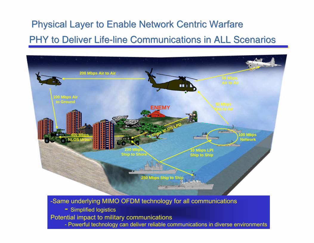
PHY to Deliver LifePHY to Deliver Life--line Communications in ALL Scenariosline Communications in ALL Scenarios
250 Mbps Ship to Ship
10 Mbps LPIShip to Ship
100 Mbps Network
50 Mbps Sea to Air
50 Mbps Air to Air
ENEMY
400 Mbps NLOS Urban
1 Mbps NLOS LPD
200 Mbps Ship to Shore
-Same underlying MIMO OFDM technology for all communications- Simplified logistics
Potential impact to military communications- Powerful technology can deliver reliable communications in diverse environments
200 Mbps Air to Air
100 Mbps Air to Ground
Physical Layer to Enable Network Centric WarfarePhysical Layer to Enable Network Centric Warfare

Wireless Integrated Systems Lab. 4
Multi Input Multi Output (MIMO) Wireless Multi Input Multi Output (MIMO) Wireless CommsComms..
1:NDEMUX
1:NDEMUX MODULATOR
MODULATOR
MODULATOR
MIMOReceiverMIMO
Receiver
ENCODERENCODER
Data
MIMO Antenna Processing
x(t)
y(t)
z(t)
r1(t) = a11x(t)+a12y(t)+a13z(t)
r3(t) = a31x(t)+a32y(t)+a33z(t)
t
Channel Impulse Response is
a series of matrices
Different data sent on different transmit antennas
The signal from each transmit antenna is received at ALL receive antennas
Channel impulse response is a matrix NxNmatrix; where N is the number of TX and RX antennas

Wireless Integrated Systems Lab. 5
MIMO Delivers 10x+ Capacity ImprovementMIMO Delivers 10x+ Capacity Improvement
10x to 20x capacity increase with same total TX power23 dB (200x) improvement in LPD/AJ properties
This is additive to improvements achieved with conventional Spread Spectrum techniques (i.e. DSSS, FHSS, …)
-9.3 dB40.8 bits/sec/Hz8x8
-4.9 dB19.0 bits/sec/Hz4x4
1.2 dB8.0 bits/sec/Hz2x2
12.8 dB2.6 bits/sec/Hz1x1
Required SNR to achieve capacity
of 1 bit/sec/Hz
95 % Capacity at 20 dB SNR
MIMO Config.
1 2 3 4 5 6 7 8 9 100
5
10
15
20
25
30
35
40
45
50
Number of receive antennas
Cap
acit
y (b
ps/
Hz)
MIMO SystemNo. TX Ant =No. RX Ant
Smart antenna array(number of transmitantenna fixed at 1)
Traditionnal 1x1SISO system
does not improve withmore antennas
95% Outage Capacity

Wireless Integrated Systems Lab. 6
Three Pronged ApproachThree Pronged Approach
Understand SISO OFDM Comm.
Complete MIMOOFDM System
Extend to MIMO
MIMO OFDMMod. ASIC
SASIC
MIMO OFDMDemod ASIC
PUZZLE
ChannelDecoupling ASIC
RELIC
FEC Encoder/decoder
COSMER
AsteriodSISO/MIMO 5.3 GHz RF
Off-Line Processing
CometMIMO-OFDM 5.3 GHz RF
Testbed complete
Big BangMIMO-OFDM 5.3 GHz RF
Real time proc. w/ ASICs
Syste
m
Testb
eds
ASICs

Wireless Integrated Systems Lab. 7
AccomplishmentsAccomplishments
• System– ML carrier and timing recovery for MIMO (ICC 2004)– Channel Estimation (PIMRC 2004)– Linear interpolation based MIMO decoding (WCNC 2004)– Scalable OFDM transceiver (VTC 2004)– Minimum wordlength requirement for MIMO OFDM (Globecom ‘03)– OFDM modeling and simulation, with Rajive Bagrodia (PADs 2004)
• VLSI– MIMO OFDM modulator – 8x8 MIMO decoder ASIC– Gbps LDPC decoder ASIC in design– MIMO OFDM demod accelerator ASIC in design
• Testbed– SISO OFDM testbed (Comm. Mag. June 2004)– MIMO OFDM testbed (Comm. Mag. Dec. 2004)– IQ mismatch cancellation (PIMRC 2004)– MIMO OFDM overhead optimization (VTC 2004)– Field measurements (Globecom 2004)

Wireless Integrated Systems Lab. 8
Maximum Likelihood Tracking Algorithm for MIMO OFDMMaximum Likelihood Tracking Algorithm for MIMO OFDM
• We derived the joint ML-optimum estimators of CFO and TFO for MIMO-OFDM– Estimators use pilot information at the output of the receiver FFTs
• No particular MIMO decoding engine is required• Simulation results show that larger MIMO configurations
allow for– Reduced number of pilot
subcarriers
– Improved estimator reliability when tracking at lower SNR
• SER simulations show that tracking performance is not sensitive to poor channel estimates

Wireless Integrated Systems Lab. 9
ˆ X (k) = minX(k )
Y(k) −H(k) ⋅ X(k)2{ }
Performance EvaluationPerformance Evaluation
• Performance was evaluated by means of simulation• Main simulation parameters mimic IEEE 802.11a setting
– 64 subcarriers (48 data + 4 pilot + 2 × 6 unused)
– 20 MHz bandwidth
– 16 samples for cyclic prefix• Channel model
– Quasi-static
– Exponentially decaying Rayleigh fading paths
– τRMS = 50 ns (⇔ 1 sample period)• Uncoded transmissions• Maximum Likelihood MIMO decoding engine

Wireless Integrated Systems Lab. 10
LowLow--Overhead Channel Estimation & AcquisitionOverhead Channel Estimation & Acquisition
• The goal of this research is to develop acquisition techniques for MIMO-OFDM with low training overhead
– Overall acquisition preamble length must be minimal• Main challenges:
– Fast MIMO channel estimation
– Fast acquisition of OFDM symbol timing
– Fast estimation of carrier frequency offset for coarse adjustment• Current focus is on channel estimation
– Approach:• Sub-sample frequency responses of individual SISO channels in order
to trade off training time with estimation accuracy• Derive maximum likelihood estimators for received signals

Wireless Integrated Systems Lab. 11
Channel Estimator Performance Channel Estimator Performance –– MSEMSE
• Mean Square Error of channel estimator shows significant overhead reduction in comparison to techniques used in IEEE 802.11a standard
0 50 100 150 200 250
-40
-35
-30
-25
-20
-15
-10
-5
0
N×M [samples]
MS
E [d
B]
v4.5.1
SNR = 0 dBSNR = 10 dBSNR = 20 dBSNR = 30 dB802.11a
Wireless Integrated Systems Lab. 12
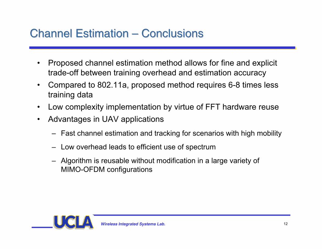
Channel Estimation Channel Estimation –– ConclusionsConclusions
• Proposed channel estimation method allows for fine and explicit trade-off between training overhead and estimation accuracy
• Compared to 802.11a, proposed method requires 6-8 times less training data
• Low complexity implementation by virtue of FFT hardware reuse• Advantages in UAV applications
– Fast channel estimation and tracking for scenarios with high mobility
– Low overhead leads to efficient use of spectrum
– Algorithm is reusable without modification in a large variety ofMIMO-OFDM configurations

Wireless Integrated Systems Lab. 13
Effect of I/Q mismatch in an OFDM systemEffect of I/Q mismatch in an OFDM system
k)X(N2
B(k)A(k)(k)*X2
B(k)A(k)k)-Y(N
k)(N*X2
B(k)A(k)X(k)2
B(k)A(k)Y(k)
−++−=
−−++=
⎥⎦
⎤⎢⎣
⎡⎥⎦
⎤⎢⎣
⎡
⎥⎦
⎤⎢⎣
⎡⎥⎦
⎤⎢⎣
⎡
DCN2
N-1 1
Frequency Subcarriers
⎥⎥⎦
⎤
⎢⎢⎣
⎡+
⎥⎥⎦
⎤
⎢⎢⎣
⎡
−⎥⎥⎥
⎦
⎤
⎢⎢⎢
⎣
⎡
+−
−+
=⎥⎥⎦
⎤
⎢⎢⎣
⎡
− )()(
)(
)(
)( )(** kV
V
kNX
kXBABA
BABA
kNY
kY k21
22
22

Wireless Integrated Systems Lab. 14
I/Q mismatch cancellation I/Q mismatch cancellation –– MMSE solutionMMSE solution
⎥⎦
⎤⎢⎣
⎡−⎥
⎥⎦
⎤
⎢⎢⎣
⎡=
⎥⎥⎦
⎤
⎢⎢⎣
⎡
− −− )()(
)(ˆ)(ˆ
)()( kNYkY
WWWW
kNXkX
NNkk
211121
⎥⎥⎦
⎤
⎢⎢⎣
⎡+
⎥⎥⎦
⎤
⎢⎢⎣
⎡
−⎥⎥⎥
⎦
⎤
⎢⎢⎢
⎣
⎡
+−
−+
=⎥⎥⎦
⎤
⎢⎢⎣
⎡
− )()(
)(
)(
)( )(** kV
V
kNX
kXBABA
BABA
kNY
kY k21
22
22
FFTWk ⎥
⎥⎦
⎤
⎢⎢⎣
⎡
− )(ˆ)(ˆ
kNXkX
Wk is the weight matrix-Trained adaptively-Works in frequency
selective channels-Works with receive
antenna diversity.-Can correct I/Q mismatch
in the presence of other impairments like CFO, phase noise, etc.
-Corrects all forms of I/Q mismatch
WYYRRX yxy == −1ˆ
MMSE solution

Wireless Integrated Systems Lab. 15
SER curves with cancellationSER curves with cancellation
10 12 14 16 18 20 22 24 26 28 3010
−5
10−4
10−3
10−2
10−1
100
SNR
SE
RSER v/s SNR with IQ mismatch cancellation
16QAM Theoretical
64QAMTheoretical
64QAM withIQ mismatchcancellation
16QAM withIQ mismatchcancellation
64QAM withcombined IQ mismatch.0.91dB gain2% of Ts delay2.81o phase
16QAM withcombined IQ mismatch.0.91dB gain2% of Ts delay2.81o phase
Wireless Integrated Systems Lab. 16
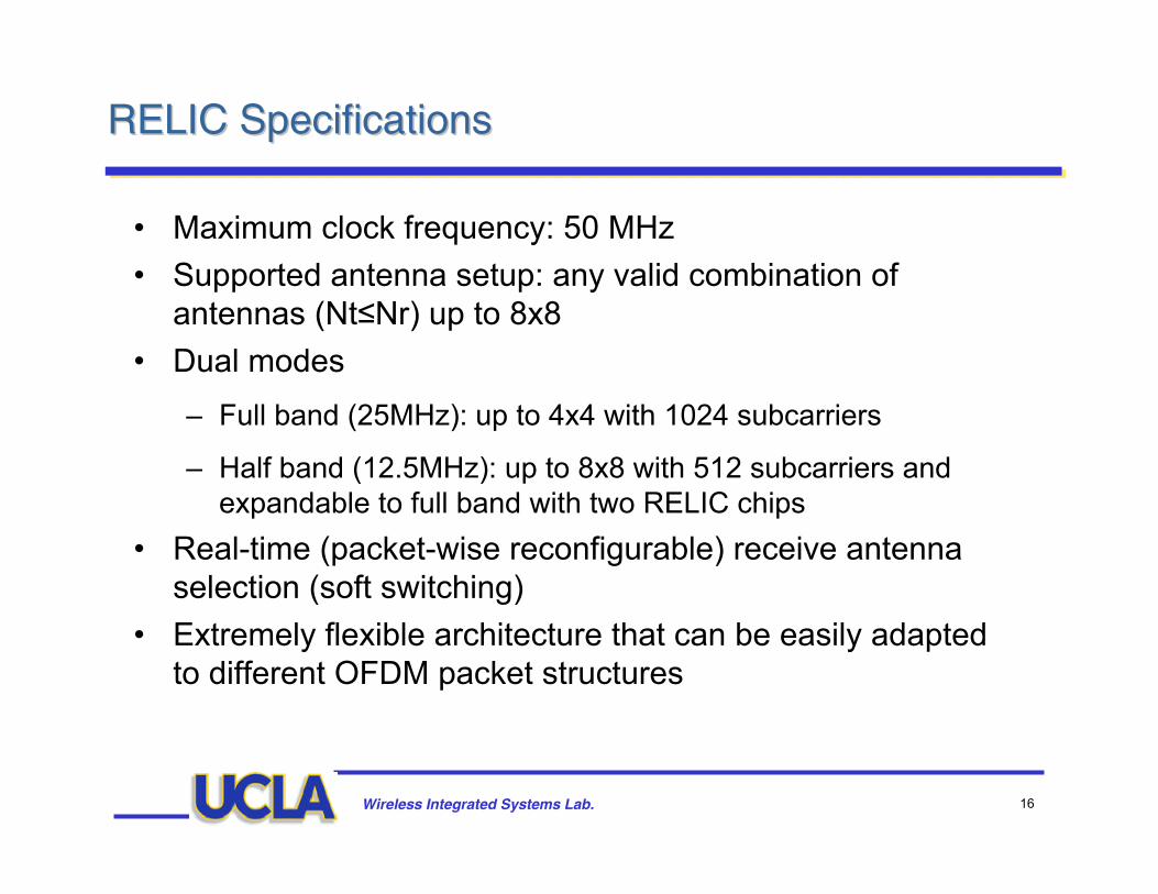
RELIC SpecificationsRELIC Specifications
• Maximum clock frequency: 50 MHz• Supported antenna setup: any valid combination of
antennas (Nt≤Nr) up to 8x8• Dual modes
– Full band (25MHz): up to 4x4 with 1024 subcarriers
– Half band (12.5MHz): up to 8x8 with 512 subcarriers and expandable to full band with two RELIC chips
• Real-time (packet-wise reconfigurable) receive antenna selection (soft switching)
• Extremely flexible architecture that can be easily adapted to different OFDM packet structures

Wireless Integrated Systems Lab. 17
V: RELIC ImplementationV: RELIC Implementation
• Process– TSMC 0.18µm CMOS
• Die Size– 39.4mm2 (core: 29.2mm2)
• Gate Count– 2.3M (SRAM: 819Kb)
• Packaging– 181-lead PGA (77 inputs, 68
outputs)• Power
– 360mW (@58MHz, 2x2 full band mode)
• Clock Frequency– 50MHz (max: 58MHz)

Wireless Integrated Systems Lab. 18
MIMO OFDM Modulator ASICMIMO OFDM Modulator ASIC
4 X 4 Switch
Ns
2Ns
3Ns
3Ns
2Ns
Ns
QAM Mapper
Data packetization and digit reversal
OFDM Modulation
PAP Reduction
IFFT
Cyclic PrefixingWindowing
Coefficient from ROM
to DACs
Delay Commutator
Stage 1 Stage 2Stage 3 Stage 4 Stage 5
Butterfly Unit

Wireless Integrated Systems Lab. 19
MIMO OFDM Transmitter ASICMIMO OFDM Transmitter ASIC
25 mm2 chip, 0.18u CMOS technology
1.6 million transistors
The first ever fully integrated MIMO OFDM transmitter operating
Implements UCLA MOBSTER packet structure
Support for 64 to 1024 pt FFT
Extreme programmability makes SASIC ideal for testbed purposes,
Wireless Integrated Systems Lab. 20
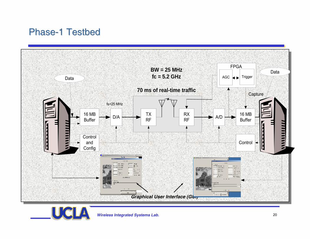
PhasePhase--1 1 TestbedTestbed
Graphical User Interface (GUI)
TXRF
RXRFD/A A/D
Controland
Config
16 MBBuffer
Control
16 MBBuffer
DataData
FPGA
AGC Trigger
Capture
fs=25 MHz
BW = 25 MHzfc = 5.2 GHz
70 ms of real-time traffic

Wireless Integrated Systems Lab. 21
TestbedTestbed ComponentsComponents
Memory BufferI/O Boards
PLX ControlBoard
Phase LockedLoop Circuit
Radio Freq.Circuit
UCLA Phase-2 2x2 MIMO Testbed

Wireless Integrated Systems Lab. 22
Controlled Field TrialsControlled Field Trials
9.2 m
9.2 m9.7 m
2.4 m
44.4 m
Corridor
Room
54-114R
oom 54-116
7.8 m
Rx Location
Tx Location
Within same room (LOS)
Between rooms (No LOS)
Corridor (No LOS)
τrms = 25 ns
τrms = 35 ns
Transmitter location changed in 5m increments12 antenna placements per location
160 Mbps 1 mW TX Power
80 Mbps 10 mW TX Power
Wireless Integrated Systems Lab. 23
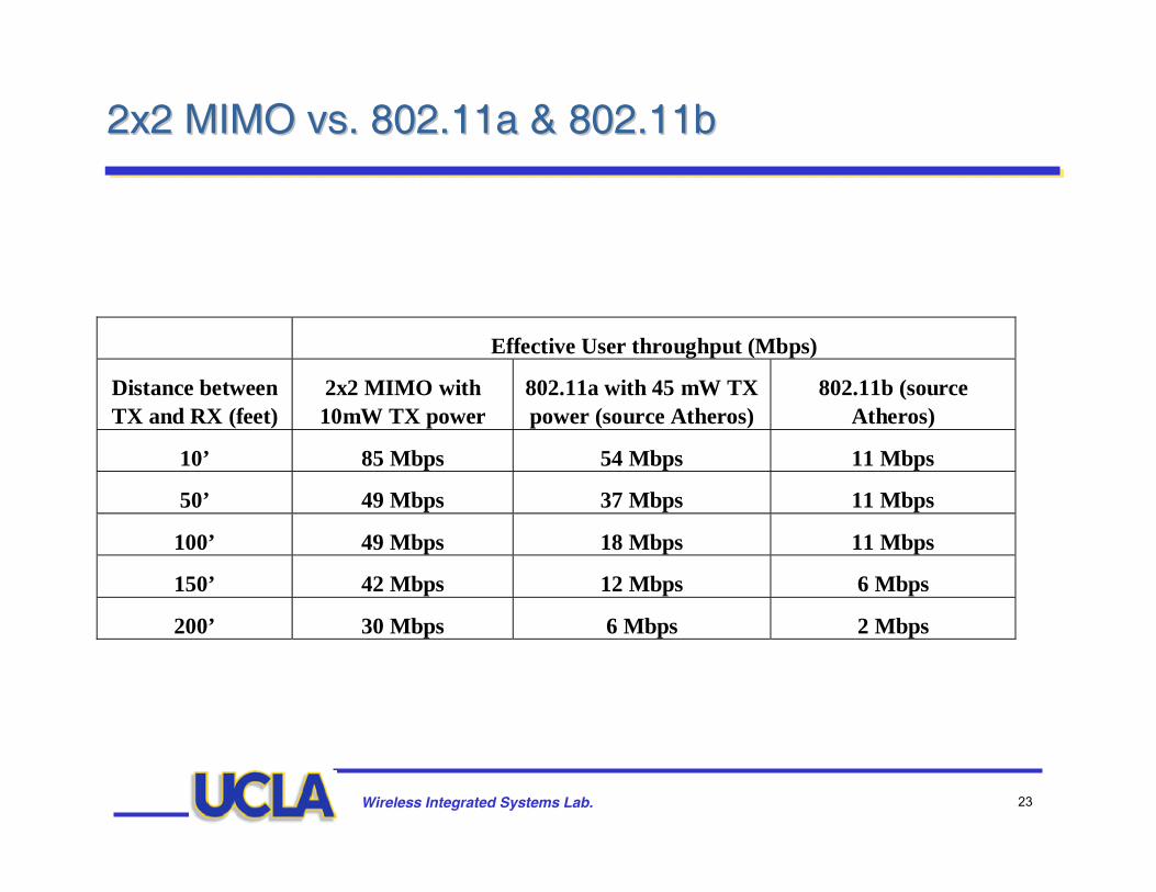
2x2 MIMO vs. 802.11a & 802.11b2x2 MIMO vs. 802.11a & 802.11b
Effective User throughput (Mbps)
Distance between TX and RX (feet)
2x2 MIMO with 10mW TX power
802.11a with 45 mW TX power (source Atheros)
802.11b (source Atheros)
10’ 85 Mbps 54 Mbps 11 Mbps
50’ 49 Mbps 37 Mbps 11 Mbps
100’ 49 Mbps 18 Mbps 11 Mbps
150’ 42 Mbps 12 Mbps 6 Mbps
200’ 30 Mbps 6 Mbps 2 Mbps
Wireless Integrated Systems Lab. 24
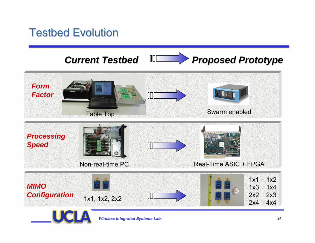
TestbedTestbed EvolutionEvolution
Form Factor
Table Top Swarm enabled
Processing Speed
Non-real-time PC
Current Current TestbedTestbed
Real-Time ASIC + FPGA
1x1, 1x2, 2x2
1x1 1x21x3 1x42x2 2x32x4 4x4
Proposed PrototypeProposed Prototype
MIMO Configuration

Wireless Integrated Systems Lab. 25
TestbedTestbed EvolutionEvolution
Multi-Band
Operation Single Band, 5.2 GHz
Bandwidth
Current Current TestbedTestbed Proposed PrototypeProposed Prototype
Operating Environment
Dual Band, 2.4 GHz + 5.2 GHz
Any Band, 400 MHz to 5.2 GHz
Fixed at 20 MHzVariable from 500 KHz to 25 MHz
Controlled Indoor Outdoor/Indoor/SeaHarsh military communication
Networking Single Link Networked Nodes

Wireless Integrated Systems Lab. 26
Two Step Transition PathTwo Step Transition Path
- Mini-Me Testbed- FOM Testbed
Wireless Integrated Systems Lab. 27
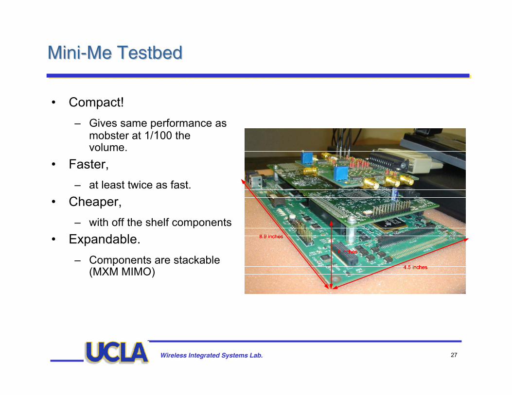
MiniMini--Me Me TestbedTestbed
• Compact! – Gives same performance as
mobster at 1/100 the volume.
• Faster, – at least twice as fast.
• Cheaper, – with off the shelf components
• Expandable. – Components are stackable
(MXM MIMO)
Wireless Integrated Systems Lab. 28
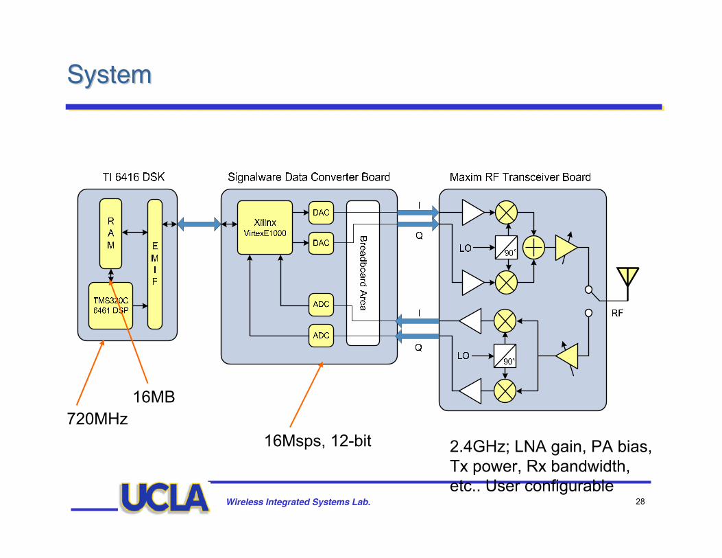
SystemSystem
720MHz16MB
16Msps, 12-bit 2.4GHz; LNA gain, PA bias, Tx power, Rx bandwidth, etc.. User configurable

Wireless Integrated Systems Lab. 29
Current statusCurrent status
• Current Status• All Mobster FOM transceiver code ported successfully to DSP.• Baseband transceiver, data converters, and RF blocks tested
independently with success.• Transmitter-DAC-RF chain completed.• RF-ADC link completed.• RF wireless link tested over the air (independently).• All steps so far are SISO.
• Pending Work• Complete ADC-baseband receiver link to close the loop.• Extend to MIMO (baseband is ready).• Migrating critical functions (e.g. block boundary detection) to
signalware’s Xilinx FPGA.• Hardware packaging.• Software packaging (leave TI code composer?).• Testing modularity by (e.g.) including LDPC or STC in a new rev.

Wireless Integrated Systems Lab. 30
Overview of the Overview of the UCLA FOMUCLA FOM
TestbedTestbed
Stephan Lang
University of California, Los Angeles

Wireless Integrated Systems Lab. 31
FOM: Small FormFOM: Small Form--FactorFactor
17 in.
12 in.7 in.
Antennas
• 4x4 MIMO system fits into 6u CPCI chassis
Wireless Integrated Systems Lab. 32
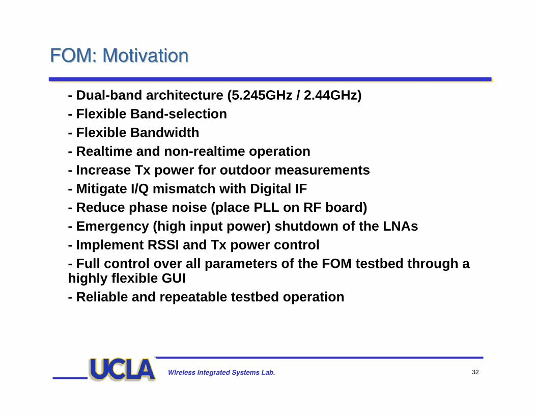
FOM: MotivationFOM: Motivation
- Dual-band architecture (5.245GHz / 2.44GHz)- Flexible Band-selection- Flexible Bandwidth- Realtime and non-realtime operation- Increase Tx power for outdoor measurements- Mitigate I/Q mismatch with Digital IF- Reduce phase noise (place PLL on RF board)- Emergency (high input power) shutdown of the LNAs- Implement RSSI and Tx power control- Full control over all parameters of the FOM testbed through a highly flexible GUI- Reliable and repeatable testbed operation

Wireless Integrated Systems Lab. 33
FOM: FrequencyFOM: Frequency--planplan
• Dual-band architecture (5.245GHz / 2.44GHz)
Wireless Integrated Systems Lab. 34
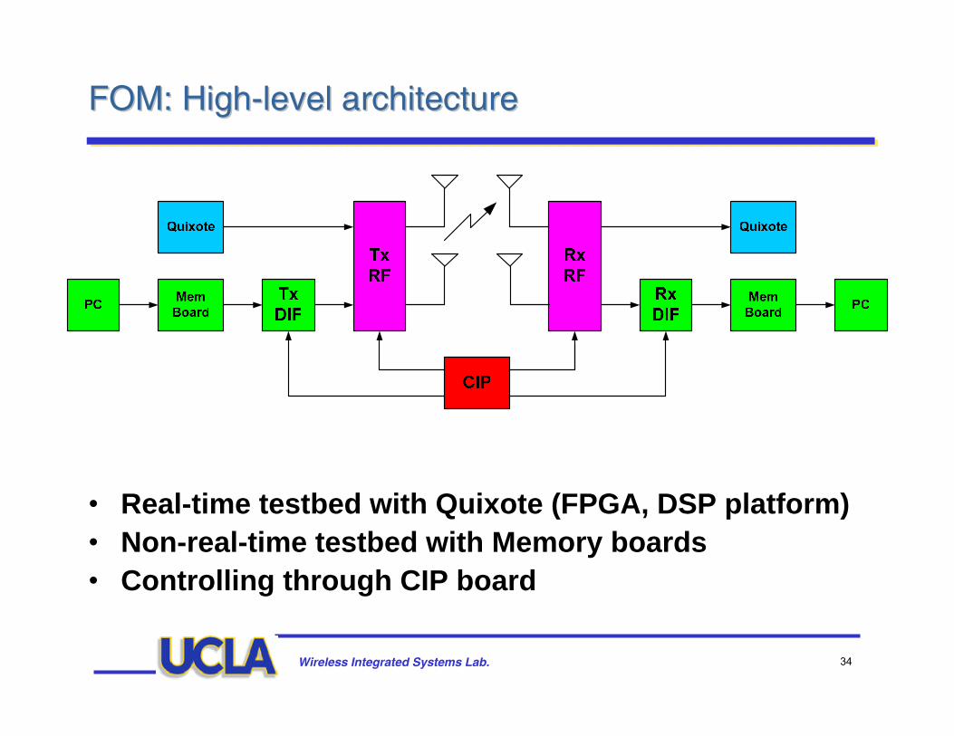
FOM: HighFOM: High--level architecturelevel architecture
• Real-time testbed with Quixote (FPGA, DSP platform)• Non-real-time testbed with Memory boards• Controlling through CIP board
Wireless Integrated Systems Lab. 35
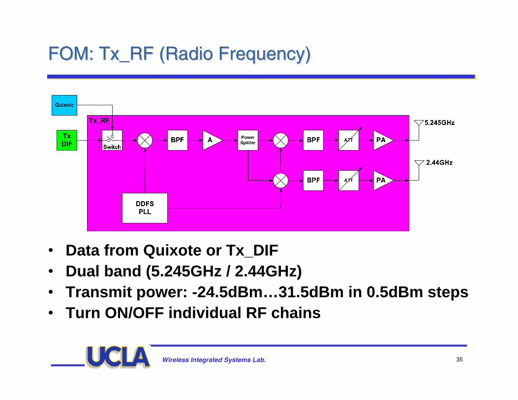
FOM: FOM: Tx_RFTx_RF (Radio Frequency)(Radio Frequency)
• Data from Quixote or Tx_DIF• Dual band (5.245GHz / 2.44GHz)• Transmit power: -24.5dBm…31.5dBm in 0.5dBm steps• Turn ON/OFF individual RF chains
Wireless Integrated Systems Lab. 36
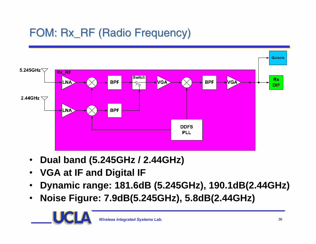
FOM: FOM: Rx_RFRx_RF (Radio Frequency)(Radio Frequency)
• Dual band (5.245GHz / 2.44GHz)• VGA at IF and Digital IF• Dynamic range: 181.6dB (5.245GHz), 190.1dB(2.44GHz)• Noise Figure: 7.9dB(5.245GHz), 5.8dB(2.44GHz)
Wireless Integrated Systems Lab. 37
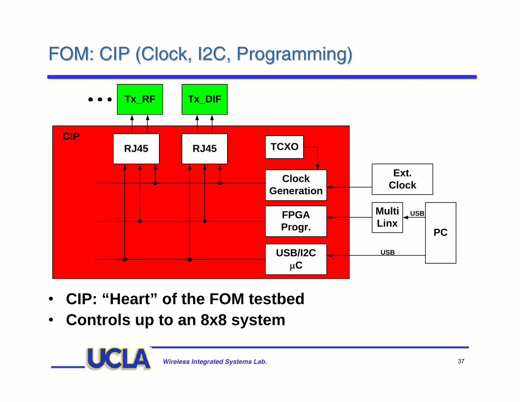
FOM: CIP (Clock, I2C, Programming)FOM: CIP (Clock, I2C, Programming)
MultiLinx
PC
USB
USB/I2CC
FPGAProgr.
USB
ClockGeneration
RJ45RJ45 TCXO
Ext.Clock
Tx_DIFTx_RF
CIP
• CIP: “Heart” of the FOM testbed• Controls up to an 8x8 system

Wireless Integrated Systems Lab. 38
FOM: FOM: Tx_DIFTx_DIF contcont’’dd
CPCI Connector
FPGA
DigitalUp Converters Power
Memory Board Connectors RJ45

Wireless Integrated Systems Lab. 39
FOM: CIP contFOM: CIP cont’’dd
RJ45 - Ports
External Clock/Trigger
Crystal Osc.
USB/I2C uC
USB Port
CPCI Connector
6.5i
n.
9in.
Wireless Integrated Systems Lab. 40
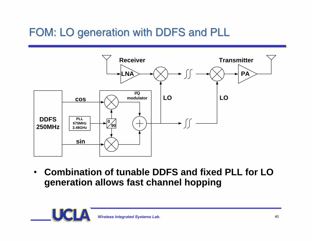
FOM: LO generation with DDFS and PLLFOM: LO generation with DDFS and PLL
• Combination of tunable DDFS and fixed PLL for LO generation allows fast channel hopping
090
I/Q modulator
PLL675MHz3.48GHz
DDFS250MHz
sin
cos
LNA
LO
PA
LO
Receiver Transmitter

Wireless Integrated Systems Lab. 41
FOM: Channel / Bandwidth SelectionFOM: Channel / Bandwidth Selection
• Re-tuning time <100ns (10us for conventional PLL)• Variable Bandwidth using Digital re-sampling• Random channel selection with DDFS

Wireless Integrated Systems Lab. 42
FOM: Flexible FOM: Flexible TestbedTestbed configurationconfiguration
• User can specify any of 8 Transceivers to operate in Tx or Rx mode
• Tx and Rx units can operate simultaneously in different bands / channels.
Wireless Integrated Systems Lab. 43
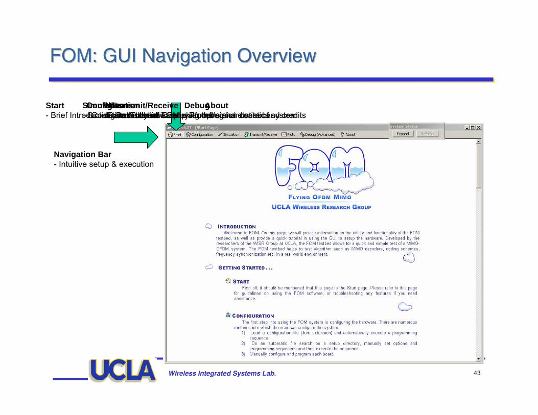
FOM: GUI Navigation OverviewFOM: GUI Navigation Overview
Navigation Bar- Intuitive setup & execution
Start- Brief Introduction and Tutorial
Configuration- Configures all hardware
Simulation- Simulation model of FOM platform
Transmit/Receive- Data transmission over the air
Plots- Data Analysis: Displays graphs and statistics
Debug- To debug hardware of system
About- Version control and credits

Wireless Integrated Systems Lab. 44
FOM: GUI Configuration OverviewFOM: GUI Configuration Overview
Click on Configuration to display hardware configuration features:
Tabs allow flipping through the 5 hardware boards:
1. CIP2. Tx Baseband3. Tx RF4. Rx Baseband5. Rx RF
First open USB connection
Light indicator shows successful connection
Settings to power up CIP board and assign I2C addresses to each board
Choose board to port connection on the CIP board CIP Board Diagram shows
which board is connected to which port
Clock / Trigger Selection
Similar configurations can be done with other boards:
Save and load configurationTo avoid tediousness, program sequence allows fast setup.
Mini-window to check the hardware status of system.
Work in progress…
Wireless Integrated Systems Lab. 45
Cognitive radio Cognitive radio –– research overviewresearch overview

Wireless Integrated Systems Lab. 46
Cognitive radioCognitive radio
• “Smart radios” – self-adaptive radio, learns its environment and adaptsby adjusting radio parameters to improve spectrum utilization
• Phases of a cognitive radio– Learning phase at receiver
• Estimation and modeling of in-band RF interference profile• Detection/sensing of spectrum holes• Channel estimation and tracking
– Feedback statistics• Feedback rate determines performance
– Adaptation phase• Dynamic spectrum management – optimize utilization of spectrum• Adaptive modulation – optimize throughput• Adaptive beamforming – minimize interference

Wireless Integrated Systems Lab. 47
Cognitive radio phasesCognitive radio phases
Radio Environment
Learn Phase•Interference analysis
•Spectrum sensing•CSI est. and tracking
Adapt Phase•Protocol define•Spectrum mgmt•Tx power control
•Beamforming
UserReq.
RF stimuli
Feedback
statistics
Transmitted
signal
Wireless Integrated Systems Lab. 48
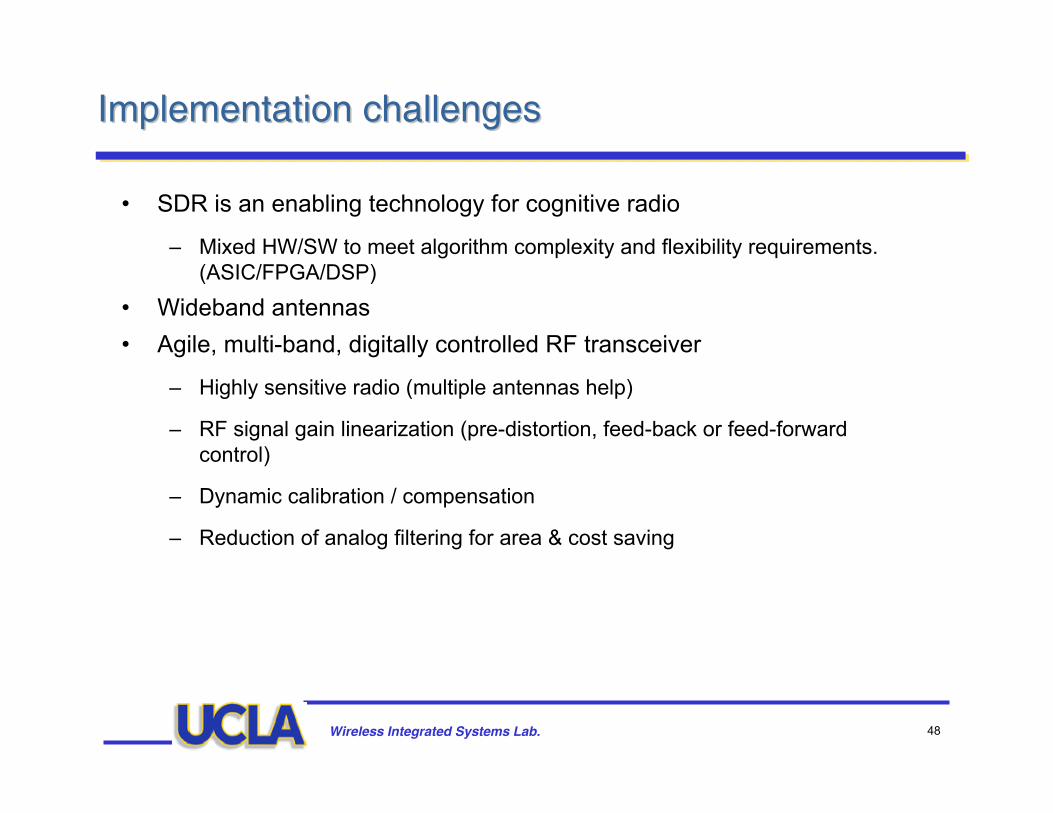
Implementation challengesImplementation challenges
• SDR is an enabling technology for cognitive radio
– Mixed HW/SW to meet algorithm complexity and flexibility requirements. (ASIC/FPGA/DSP)
• Wideband antennas• Agile, multi-band, digitally controlled RF transceiver
– Highly sensitive radio (multiple antennas help)
– RF signal gain linearization (pre-distortion, feed-back or feed-forward control)
– Dynamic calibration / compensation
– Reduction of analog filtering for area & cost saving

Wireless Integrated Systems Lab. 49
Learning PhaseLearning Phase
A/D Window Time-FreqAnalysis
Detectholes
Channel Est
Interferenceanalysis Q
UANTIZE
FeedbackTo Tx

Wireless Integrated Systems Lab. 50
Adaptation PhaseAdaptation Phase
SpectrumMgmt
Beamformingalgorithm
Scheduler(MAC)
Link Optimizer
SDR SDR
Physical layerspecification
Feedbackstatistics
Wirelesslink
Wireless Integrated Systems Lab. 51
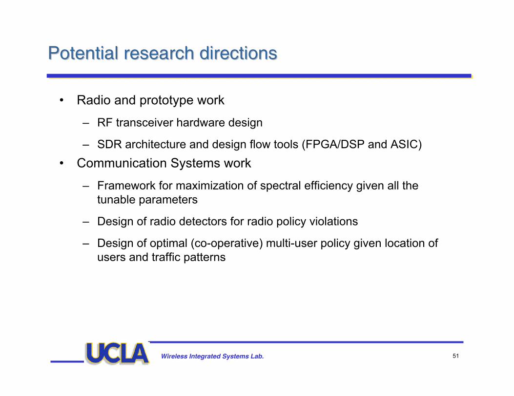
Potential research directionsPotential research directions
• Radio and prototype work
– RF transceiver hardware design
– SDR architecture and design flow tools (FPGA/DSP and ASIC)• Communication Systems work
– Framework for maximization of spectral efficiency given all the tunable parameters
– Design of radio detectors for radio policy violations
– Design of optimal (co-operative) multi-user policy given location of users and traffic patterns