modbus plus interface option manual - novatech | … speed peer to peer token passing network...
TRANSCRIPT

MultiComm & MultiComm RTH
Modbus Plus Interface Option Manual
August 10, 2009 ML0006 Document © 2009 by Bitronics, LLC
MTWIE4(A,B), MTWDE4(A,B) 3 Element 4 Wire MTWIEC4(A,B), MTWDEC4(A,B) (WYE) MTWIE5(A,B), MTWDE5(A,B) 2 Element 3 Wire MTWIEC5(A,B), MTWDEC5(A,B) (DELTA) MTWIE6(A,B), MTWDE6(A,B) 2½ Element 4 Wire
(WYE) Firmware Version 3.60 and Later Includes Information on CI1 Option (1 Amp Inputs)

ML0006 October 2009 Copyright 2009 Bitronics, LLC. i
TABLE OF CONTENTS TABLE OF CONTENTS ................................................................................................ i CERTIFICATION ........................................................................................................... ii COPYRIGHT ................................................................................................................. ii INSTALLATION AND MAINTENANCE ......................................................................... ii WARRANTY AND ASSISTANCE .................................................................................. ii 1.0 DESCRIPTION ........................................................................................................ 1
1.1 Introduction ........................................................................................................ 1 1.2 Features ............................................................................................................. 1 1.3 Specifications ..................................................................................................... 1
2.0 PRINCIPLES OF OPERATION ............................................................................... 3
2.1 Modular Construction ......................................................................................... 3 2.2 Modbus Plus Connector Board .......................................................................... 3 2.3 Modbus Plus Peer Processor ............................................................................. 3
3.0 MODBUS PLUS INTERFACE ................................................................................. 4
3.1 Introduction ........................................................................................................ 4 3.2 MultiComm Modbus Plus ................................................................................... 5 3.3 Modbus Plus Routing Address ........................................................................... 5 3.4 Transaction Timing ............................................................................................ 6 3.5 Data Format ....................................................................................................... 7
3.5.1 Instantaneous Registers 2½ or 3 Elem ................................................... 9 3.5.2 Demand Registers 2½ or 3 Elem .......................................................... 12 3.5.3 RTH Summary Registers 2½ or 3 Elem ............................................... 13 3.5.4 RTH Individual Registers 2½ or 3 Elem ................................................ 15 3.5.5 Instantaneous Registers 2 Elem ........................................................... 17 3.5.6 Demand Registers 2 Elem .................................................................... 20 3.5.7 RTH Summary Registers 2 Elem .......................................................... 21 3.5.8 RTH Individual Registers 2 Elem .......................................................... 23
3.6 Writeable Registers .......................................................................................... 25 3.6.1 Setting CT & PT Ratios ......................................................................... 25 3.6.2 Resetting Energy & Demand ................................................................ 25 3.6.3 TDD Writeable Denominators ............................................................... 26 3.6.4 Display Screen Configuration Registers .............................................. 26 3.6.5 Communication Configuration Registers ............................................. 27 3.6.6 Tag Register ........................................................................................ 28
3.7 Converting Data to Engineering Units .............................................................. 28 3.8 Health Check ................................................................................................... 32 3.9 Diagnostic LED ................................................................................................ 33 3.10 Heartbeat State Counter ............................................................................... 33 3.11 Meter ID Register .......................................................................................... 34
4.0 INSTALLATION ..................................................................................................... 35
4.1 Setting Modbus Plus Address .......................................................................... 35 4.2 Modbus Plus Cable .......................................................................................... 38

ML0006 October 2009 Copyright 2009 Bitronics, LLC. ii
CERTIFICATION Bitronics, LLC certifies that the calibration of its products are based on measurements using equipment whose calibration is traceable to the United States National Institute of Standards Technology (NIST). COPYRIGHT This Option Manual is copyrighted and all rights are reserved. The distribution and sale of this manual are intended for the use of the original purchaser or his agents. This document may not, in whole or part, be copied, photocopied, reproduced, translated or reduced to any electronic medium or machine-readable form without prior consent of Bitronics, LLC, except for use by the original purchaser. INSTALLATION AND MAINTENANCE Bitronics' products are designed for ease of installation and maintenance. As with any product of this nature, however, such installation and maintenance can present electrical hazards and should only be performed by properly trained and qualified personnel. If the equipment is used in a manner not specified by Bitronics, the protection provided by the equipment may be impaired. WARRANTY AND ASSISTANCE Products manufactured by Bitronics, LLC are warranted against defects in materials and workmanship for a period of thirty-six (36) months from the date of their original shipment from the factory. Products repaired at the factory are likewise warranted for eighteen (18) months from the date the repaired product is shipped, or for the remainder of the product’s original Warranty, whichever is greater. Obligation under this warranty is limited to repairing or replacing, at Bitronics' factory, any part or parts which Bitronics' examination shows to be defective. Warranties only apply to products subject to normal use and service. There are no warranties, obligations, liabilities for consequential damages, or other liabilities on the part of Bitronics except this Warranty covering the repair of defective materials. The warranties of merchantability and fitness for a particular purpose are expressly excluded. For assistance, contact Bitronics LLC at: Telephone: 610.997.5100 Fax: 610.997.5450 Email: [email protected] Website: www.novatechweb.com/bitronics Shipping: 261 Brodhead Road Bethlehem, PA 18017-8698 USA

ML0006 October 2009 Copyright 2009 Bitronics, LLC. iii

ML0006 October 2009 Copyright 2009 Bitronics, LLC. 1
1.0 DESCRIPTION 1.1 Introduction The Modbus Plus 1 protocol option for the MultiComm and MultiComm RTH family of instruments is designed to allow operation of these instruments on MODBUS PLUS networks. The MultiComm and MultiComm RTH meters are MODICON certified, and can connect directly to MODBUS PLUS networks. The MODBUS PLUS protocol is a high speed peer to peer token passing network designed by Modicon. The MODBUS PLUS network allows a wide variety of devices and topologies. 1.2 Features
* Rugged Bitronics design
* Dedicated communications processor: fast response for maximum instrument polling rates.
* User selectable instrument address with pushbutton front panel display
* MODBUS PLUS network status/diagnostic LED visible from front panel
* Simple command to read any number of instrument quantities
* Simple energy reset and demand reset commands
* Data available through HOLDING REGISTER READ and/or GLOBAL DATA
* Supports remote setting of CT and PT scaling factors and display screen setup
* MODICON Certified 1.3 Specifications Resolution:
Amperes: 0.1% of 5* A nominal
Volts: 0.07% of 120V nominal
Frequency: 0.01 Hz
* - When CT1 Option (1Amp Input) is installed, divide this value by 5
1 - MODICON®, MODBUS® and Modbus Plus are trademarks of Schneider Electric.

ML0006 October 2009 Copyright 2009 Bitronics, LLC. 2
1.3 Specifications, Cont’d
Watts/VARs/VAs:
Per Phase: 0.1% of 500* secondary Watts nominal Total: 0.1% of 1500* secondary Watts nominal (2 ½ or 3 ELEMENT)
0.1% of 1000* secondary Watts nominal (2 ELEMENT)
Power Factor: 0.001 K Factor: 0.01 TDD, THD: 0.1%
Accuracy: Same as base meter (0.25% Class per ANSI Std 460-1988) Modbus Plus
Connector: 9-pin D-connector for shielded twisted pair Modbus Plus
Communication: Modbus Plus 1 Megabit per second
Distance: 1,500 ft (450m) per section, 6,000 ft (1800m) with repeaters
Functions: Global Data and Read Holding Registers (FUNC 3) Preset Single Register (FUNC 6) and Preset Multiple Register (FUNC 16) for Writeable Registers Only Diagnostics (FUNC 8 - SUBFUNC 21) Get/Clear Network Statistics
Response Time:
Model Response Time
MAX (TYP) Global Data
Updated
All 8 Task
Paths Serviced MAX
MTWIE(C)_A 650ms (300ms) 600ms
650ms
MTWDE(C)_A 650ms (300ms) 600ms
650ms
MTWIE(C)_B 150ms (75ms) 100ms1
150ms
MTWDE(C)_B 200ms (100ms) 150ms1
200ms
1 - No READ or WRITE requests and input 56Hz to 75Hz, otherwise use Max Response Time
Addressability: Modbus Plus Device Node Addresses 1 .. 64
Task Path Addresses 1 .. 8
Mode: Host Device (must specify task path in routing address) EEPROM Memory Endurance:
CT\PT Ratios: 1,000,000 minimum CT\PT ratio changes (CT\PT ratio writes) * - When CT1 Option (1Amp Input) is installed, divide this value by 5

ML0006 October 2009 Copyright 2009 Bitronics, LLC. 3
2.0 PRINCIPLES OF OPERATION 2.1 Modular Construction The Bitronics MultiComm Modbus Plus Option is composed of two major modules. The Modbus Plus network connects to the output connector board which in turn is driven by the by the Modbus Plus Peer processor. 2.2 Modbus Plus Connector Board The Modbus Plus network connection is made via the DB-9 connector on the back of the instrument. An EARTH GROUND input is provided by a #10-32 brass stud, also located on the rear cover of the instrument. WARNING - DO NOT over-tighten the nuts on the input connections, HAND tighten with a standard nutdriver, 12 inch-pounds is recommended, MAXIMUM torque is 15 inch-pounds. This EARTH GROUND connection is required for proper Modbus Plus operation, and should be connected to a good earth ground. Both the DB9 and the Earth Ground input are connected to the Modbus Plus Connector Board, which also contains transformer and capacitive isolation of the meter from the actual Modbus Plus cable. The shield of the Modbus Plus cable is connected to the EARTH GROUND terminal through a transient protection network. A flexible circuit connects this board with the Modbus Plus PEER Processor Board (see Figure 2 for schematic). 2.3 Modbus Plus PEER Processor Board The Modbus Plus PEER Processor Board contains an Intel 80C152JA communications controller and its associated circuitry. This processor handles all the token-passing, error detecting, message transaction and other network overhead required by the Modbus Plus network. When the PEER processor receives a Modbus Plus message, it checks if the Modbus Plus ADDRESS is the address of this node. The NODE ADDRESS is set via two 16-position rotary switches SW3 and SW4, which are also located on this board (See section 4.1 for instructions on setting the NODE ADDRESS). If the Modbus Plus address matches this node, the peer processor passes the transaction message through the DUAL-PORT RAM to the HOST processor. The HOST processor then completes the transaction, and sends a response through the DUAL-PORT RAM back to the PEER processor, which then sends the appropriate Modbus Plus message on the network. The transceiver IC is also located on this board. This IC provides the drive to transmit and receive messages on the Modbus Plus cable. The transceiver is connected to the Modbus Plus Connector Board via a Kapton ribbon cable which plugs into a three pin connector on the front of the electronics module. Status of the Modbus Plus network at this node is indicated by the Modbus Plus Diagnostic LED which is located in the upper left hand corner of the PEER processor board. This Diagnostic LED is visible through the faceplate, and can been seen in the upper left hand corner of the upper display. Section 3.9 describes the operation of the Diagnostic LED.

ML0006 October 2009 Copyright 2009 Bitronics, LLC. 4
The CT/PT switch and the select pushbutton are also mounted on the PEER Processor Board, however both these switches are read by the HOST processor. A second pushbutton switch is mounted on the faceplate, and connected to the Peer Processor board via a pair of wires and a connector. This switch is connected in parallel with the select switch mounted on the Peer Processor board, and is used to stop and start the scrolling of the front display. Refer to the MultiComm Alpha Series Users Manual for detailed information concerning the display. 3.0 MODBUS-PLUS INTERFACE 3.1 Introduction The Modbus Plus network is a local area network originally designed for industrial control applications, which has recently been applied to a wide range of utility applications. The network enables programmable controllers, host computers, MMIs and a wide variety of other devices (such as Bitronics MultiComm instruments) to communicate throughout an industrial plant or substation. The network supports up to 64 addressable node devices at a data rate of 1 million bits per second. Up to 32 devices can connect directly to the network cable (shielded twisted pair) over a length of 1500 feet (450 meters). Repeater devices are used to extend the cable distance to 6000 feet (1800 meters) and to allow connection to all 64 node devices. The network is a physical bus, in that all nodes are attached to a piece of cable. At each end of the cable must be a terminator. This terminator prevents unwanted electrical reflections of the signal sent on the network cable. Modicon sells Modbus Plus cable connectors that come in two types. Inline connectors are dark grey in color and are used in the middle of a Modbus Plus network cable. Special terminating connectors that are light grey contain the terminator, and are used at both ends of the Modbus Plus cable. Multiple Modbus Plus networks can be joined through Bridge Plus or similar devices. Messages originating at a node on one network can be routed through one or more bridges to a destination node on another network. Data is passed through bridges to other networks only when needed. Logically, the network is a ring, a token ring to be more specific. Network nodes are identified by addresses assigned by the user. Each node's address is independent of its physical site location. Addresses are within the range of 1 to 64 decimal, and do not have to be sequential. Duplicate addresses are not allowed. Network nodes function as peer members of a logical ring, gaining access to the network upon receipt of a token frame. The token is a grouping of bits that is passed in a rotating address sequence from one node to another. Where multiple networks are joined by a bridge or bridges, the token is not passed through the bridge device. Each network maintains its own token rotation sequence independently of the other networks. While holding the token, a node initiates message transactions with other nodes. Each message contains routing fields that define the source and destination, including its routing path through bridges to the final destination node on a remote network.

ML0006 October 2009 Copyright 2009 Bitronics, LLC. 5
When passing the token, a node can write into a global database that is broadcast to all nodes on the network. Each node has a maximum of 32 global data registers ( 16 bits each ) that it can write. Global data is transmitted as a field within the token frame. Other nodes monitor the token pass and can extract the global data. Each node therefore maintains its own copy of the global database (64 nodes x 32 global data registers/node) which allows for rapid updating of alarms, setpoints and other data. Each network maintains its own unique global database, as the token is not passed through a bridge to another network. For more information, the manual "MODICON MODBUS PLUS NETWORK PLANNING AND INSTALLATION GUIDE" (GM-MBPL-001) may be purchased for a nominal fee directly from Modicon Inc. 3.2 MultiComm Modbus Plus Implementation The Modbus Plus implementation in the MultiComm instrument conforms to all the standard Modbus Plus specifications and capabilities, such as maximum nodes, distance, signal sensitivity, etc. The MultiComm instrument is classified as a HOST-BASED DEVICE in the Modbus Plus structure. Of the 44 data items (70 data items in transducers with demand measurements, 341 data items in transducers with demand and harmonics measurements) that are available from the MultiComm instrument , 27 (31 in “B” Versions) can be obtained via the Modbus Plus Network via GLOBAL DATA. Global Data is a common data base shared by all nodes on a MODBUS PLUS network. Any of the 44 data items (70 on transducers with demand measurements, 341 data items in transducers with demand and harmonics measurements) can be read directly by issuing a READ HOLDING REGISTERS command from the requesting node. 3.3 Modbus Plus Routing Address The MODBUS PLUS routing address is 5 bytes long. This allows for communications over one or more Bridge Plus devices that connect two separate MODBUS PLUS networks together. Because the MultiComm instrument is a HOST-BASED DEVICE, the Modbus Plus address must contain two routing addresses. The next-to-last NON-ZERO byte is the PHYSICAL ADDRESS (1-64) of the meter. The last NON-ZERO byte in the routing field is the TASK PATH NUMBER (1-8) inside the meter. If you are familiar with addressing MODICON's PLCs, you will notice that the routing path is slightly different. When addressing PLCs it is not necessary to specify a task path number in the routing field. This is because the task path number is automatically selected inside a PLC designated device. In a HOST designated device, the task path number is NOT automatically selected, so it is necessary to specify it in the routing address field. Since the address of the meter and the task number each require 1 byte of information, the remaining 3 bytes allow for communications through one, two or three Bridge Plus devices. Example 1: Communications to a node on the same network.
42.4.0.0.0 Meter address #42, task path #4

ML0006 October 2009 Copyright 2009 Bitronics, LLC. 6
Example 2: Communications to a node on another MODBUS PLUS network connected by one Bridge Plus device. 33.42.4.0.0 Bridge address #33 on local network, Meter address
#42, task path #4 Example 3: Communications to a node on another MODBUS PLUS network connected
by three Bridge Plus devices. 21.5.63.42.4 1st Bridge address #21 on local network
2nd Bridge address #5 on next network 3rd Bridge address #63 on the subsequent network Meter address #42 Task path #4
When reading register(s) of the MultiComm instrument from different requesting devices, it is recommended to use a different task path number for each of the separate requesting devices. This will prevent contention when the two requesting devices try to read the meter at the same time. 3.4 Transaction Timing The MultiComm instruments complete an entire set of calculations approximately every 150 milliseconds (600msec for non “B” Versions). At the completion of the calculation the HOST processor updates the GLOBAL DATA in the PEER, and then the HOST processor also services any pending transactions on the eight task paths. All eight tasks are serviced at this time, however they are serviced only once. If a transaction is received on a task path that has just been serviced, that request will be serviced after the next set of calculations are completed (max response time).
Model
Response Time
MAX (TYP) Global Data
Updated All 8 Task Paths Serviced MAX
MTWIE(C)4A,5A,6A
650ms (300ms) 600ms 650ms
MTWDE(C)4A,5A,6A
650ms (300ms) 600ms 650ms
MTWIE(C)4B,5B,6B
150ms (75ms) 100ms1 150ms
MTWDE(C)4B,5B,6B
200ms (100ms) 150ms1 200ms
1 - No READ or WRITE requests and input 56Hz to 75Hz, otherwise use Max Response Time.
The Energy and Demand registers can be RESET by writing the appropriate value to Holding Register 40100. The resets and their associated values are listed in Table 1 (see Section 3.2). The Registers will be reset within 0.6 seconds, however it takes the meter 5 seconds to clear the energy data stored in the EEPROM and up to 10 seconds to reset the demand data stored in EEPROM. The USER must ensure that the power is not interrupted to the meter for this 5 or 10 second period after this command is issued.

ML0006 October 2009 Copyright 2009 Bitronics, LLC. 7
The CT/PT Ratio and Divisor Registers (40041-40044), TDD Amps Denominators (40101-40103), Tag Register (40099) and the Display Setup Registers (40092-40096) can be set by writing to the proper register. The registers will be written to EEPROM within 700 milliseconds. 3.5 Data Format The MultiComm instrument contains a set of holding registers (4XXXX) into which the instrument places values that correspond to the measurements the instrument is making. These holding registers can be read by any other device on the network using a READ HOLDING REGISTER or READ DATA command. The MultiComm instrument also writes 27 words of data (31 words for any “B” version) to the Modbus Plus GLOBAL DATA SPACE. Every node on this network maintains this data in its own memory. The global data is accessed by using the MSTR function block (in a PLC). Users of other devices are advised to refer to their specific user's guide to determine how their device handles GLOBAL DATA. GLOBAL DATA is not transmitted across BRIDGES, nor is it transmitted to Modbus devices connected via a BRIDGE-PLUS. For both GLOBAL DATA and HOLDING REGISTER DATA, the Health Check Register should always be read and checked before interpreting data, since some failure modes will cause erroneous data to be presented (See Section 3.8). The data is represented in OFFSET BINARY format, for conversion of the register data into ENGINEERING UNITS, please refer to Section 3.7. For specifics concerning the correct command and its implementation, users are directed to the User's manual for the specific device that will request the data. Listed on the following pages are the register assignments for the MultiComm instruments. The available registers depend upon the particular model of MultiComm instrument. The registers have been broken down into four blocks, which are shown in Figure 1. These various blocks are listed on the following pages. Table 2 indicates which blocks pertain to which models. The registers are also divided into two sections by Element Type, 2½ or 3 Element models are in the first section, and 2 Element models are in the second section. Note that unless otherwise specified, all registers are READ-ONLY. Models
Instan- taneous
Demand RTH Summary
RTH Individuals
Element Type
MTWIE(C)4A,6A,4B,6B
X
3 / 2½
MTWIE(C)5A,5B
X
2
MTWDE(C)4A,6A
X X
3 / 2½
MTWDE(C)5A
X X
2
MTWDE(C)4B,6B
X X X X
3 / 2½
MTWDE(C)5B
X X X X
2

ML0006 October 2009 Copyright 2009 Bitronics, LLC. 8

ML0006 October 2009 Copyright 2009 Bitronics, LLC. 9
3.5.1 INSTANTANEOUS Data Registers for 2 ½ or 3 Element Models
Quantity Holding Register
Global Register
Representation
Health Check 40001 1 Refer to Section 3.8 Amperes Phase A 40002 2 | Amperes Phase B 40003 3 | 2047 = 0Amps; 4095 = 10.0*AmpsAmperes Phase C 40004 4 | Volts Phase A-N 40005 5 | Volts Phase B-N 40006 6 | 2047 = 0Volts; 4095 = 150.0VoltsVolts Phase C-N 40007 7 | Watts Total 3 Phase 40008 8 0 = -3000*Watts; 2047 = 0Watts;
4095 = +3000*Watts VARs Total 3 Phase 40009 9 0 = -3000*VARs; 2047 = 0VARs;
4095 = +3000*VARs Watts Phase A 40010 10 | 0 = -1000*Watts; 2047 = 0WattsWatts Phase B 40011 11 | 4095 = +1000*Watts Watts Phase C 40012 12 | VARs Phase A 40013 13 | 0 = -1000*VARs; 2047 = 0VARsVARs Phase B 40014 14 | 4095 = +1000*VARs VARs Phase C 40015 15 | CT Ratio 40016 16 | Normalized ratio (Does not include PT Ratio 40017 17 | decimal point)
| 500< Ratio <9999 (CT:5) or | (CT:1 with CT1 option) | 1000 < Ratio < 9999 (PT:1)
Neutral Current 40018 18 2047 = 0Amps; 4095 = 15.0*Amps + kWatthour (High) 40019 19 0=0kWh; 9999=99,990,000kWh+ kWatthour (Low) 40020 20 0=0kWh; 9999=9,999kWh - kWatthour (High) 40021 21 0=0kWh; 9999=-99,990,000kWh- kWatthour (Low) 40022 22 0=0kWh; 9999=-9,999kWh + kVARhour (High) 40023 23 0=0kVARh; 9999=99,990,000kVARh+ kVARhour (Low) 40024 24 0=0kVARh; 9999=9,999kVARh - kVARhour (High) 40025 25 0=0kVARh; 9999=-99,990,000kVARh- kVARhour (Low) 40026 26 0=0kVARh; 9999=-9,999kVARh * - When CT1 Option (1Amp Input) is installed, divide this value by 5

ML0006 October 2009 Copyright 2009 Bitronics, LLC. 10
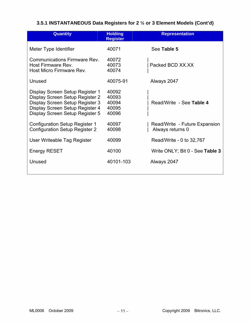
3.5.1 INSTANTANEOUS Data Registers for 2 ½ or 3 Element Models (Cont’d)
Quantity Holding Register
Global Register
Representation
Frequency 40027 27 0 = <45.00Hz; 4500 = 45.00Hz
7500 = 75.00Hz; 9999 =>75.00Hz Unused 40028 282 | Unused 40029 291 | Always 2047 Unused 40030 301 | Heartbeat State Counter 40031 31 See Section 3.10 Unused 40032 N/A Always 2047 VAs Phase A 40033 N/A | VAs Phase B 40034 N/A | 2047 = 0VA; 4095 = 1000*VA VAs Phase C 40035 N/A | VAs Total 3 Phase 40036 N/A 2047 = 0VAs; 4095 = 3000*VAs PF Phase A 40037 N/A | 1047 = -1; 2047 = 0; 3047 = +1 PF Phase B 40038 N/A | 4046 = Amps or Volts too low PF Phase C 40039 N/A | (-) lagging; (+) leading PF Total 3 Phase 40040 N/A 1047 = -1; 2047 = 0; 3047 = +1
4046 = Amps or Volts too low (-) lagging; (+) leading
CT Ratio 40041 N/A Read/Write normalized ratio,
copied to 40016 CT Ratio Divisor 40042 N/A Read/Write; = 1,10,100, or 1000 PT Ratio 40043 N/A Read/Write normalized ratio,
copied to 40017 PT Ratio Divisor 40044 N/A Read/Write; = 1,10,100, or 1000 Unused 40045-70 N/A Always 2047 * - When CT1 Option (1Amp Input) is installed, divide this value by 5
2 “B” Version Instruments Only
ML0006 October 2009 Copyright 2009 Bitronics, LLC. 11
3.5.1 INSTANTANEOUS Data Registers for 2 ½ or 3 Element Models (Cont’d)
Quantity Holding Register
Representation
Meter Type Identifier 40071 See Table 5 Communications Firmware Rev. 40072 | Host Firmware Rev. 40073 | Packed BCD XX.XX Host Micro Firmware Rev. 40074 | Unused 40075-91 Always 2047 Display Screen Setup Register 1 40092 | Display Screen Setup Register 2 40093 | Display Screen Setup Register 3 40094 | Read/Write - See Table 4 Display Screen Setup Register 4 40095 | Display Screen Setup Register 5 40096 | Configuration Setup Register 1 40097 | Read/Write - Future Expansion Configuration Setup Register 2 40098 | Always returns 0 User Writeable Tag Register 40099 Read/Write - 0 to 32,767 Energy RESET 40100 Write ONLY; Bit 0 - See Table 3 Unused 40101-103 Always 2047

ML0006 October 2009 Copyright 2009 Bitronics, LLC. 12
3.5.2 DEMAND Data Registers for 2 ½ or 3 Element Models
Quantity Holding Register
Representation
Present Demand Amps φA 40045 |Present Demand Amps φB 40046 | 20471 = 0Amps; 4095 = 10.0*Amps Present Demand Amps φC 40047 | Max Demand Amps φA 40048 | Max Demand Amps φB 40049 | 20471 = 0Amps; 4095 = 10.0*Amps Max Demand Amps φC 40050 | Present Demand Amps N 40051 20471 = 0Amps; 4095 = 15.0*Amps Max Demand Amps N 40052 20471 = 0Amps; 4095 = 15.0*Amps Present Demand Volts φA 40053 | Present Demand Volts φB 40054 | 20471 = 0Volts; 4095 = 150.0Volts Present Demand Volts φC 40055 | Max Demand Volts φA 40056 | Max Demand Volts φB 40057 | 20471 = 0Volts; 4095 = 150.0Volts Max Demand Volts φC 40058 | Min Demand Volts φA 40059 | Min Demand Volts φB 40060 | 20471 = 0Volts; 4095 = 150.0Volts Min Demand Volts φC 40061 | Present Demand Watts Total 40062 | 0 = -3000*Watts; 20471 = 0Watts Max Demand Watts Total 40063 | 4095 = +3000*Watts Min Demand Watts Total 40064 | Present Demand VARs Total 40065 | 0 = -3000*VARs; 20471 = 0VARs Max Demand VARs Total 40066 | 4095 = +3000*VARs Min Demand VARs Total 40067 | Present Demand VAs Total 40068 | Max Demand VAs Total 40069 | 20471 = 0VAs; 4095 = +3000*VAs Min Demand VAs Total 40070 | Amp Demand RESET 40100 Read/Write Bit 1 - See Table 3 Volt Demand RESET 40100 Read/Write Bit 2 - See Table 3 Power Demand RESET 40100 Read/Write Bit 3 - See Table 3 * - When CI1 Option (1Amp Input) is installed, divide this value by 5 1 - MTWIExB models always return the value 2047

ML0006 October 2009 Copyright 2009 Bitronics, LLC. 13
3.5.3 RTH SUMMARY Data Registers for 2 ½ or 3 Element Models
Quantity Holding Register
Representation
Amp Demand RESET 40100 Read/Write Bit 1 - See Table 3 Volt Demand RESET 40100 Read/Write Bit 2 - See Table 3 Power Demand RESET 40100 Read/Write Bit 3 - See Table 3 Harmonic Demand RESET 40100 Read/Write Bit 4 - See Table 3 TDD Denominator Amps φA 40101 | Read/Write 20471 = 0Amps; TDD Denominator Amps φB 40102 | 4095 = 10.0*Amps. If reg = 2047, then TDD Denominator Amps φC 40103 | Fund Amps will be used (THD)
| Factory Default = 5* Amps Secondary Fundamental Amps φA 40104 | Fundamental Amps φB 40105 | 2047 = 0Amps; 4095 = 10.0*Amps Fundamental Amps φC 40106 | Fundamental Amps Neutral 40107 2047 = 0Amps; 4095 = 15.0*Amps Fundamental Volts φA 40108 | Fundamental Volts φB 40109 | 2047 = 0Volts; 4095 = 150.0Volts Fundamental Volts φC 40110 | TDD2 Amps φA 40111 | TDD2 Amps φB 40112 | 0 = 0.0%; 9999 = 999.9% TDD2 Amps φC 40113 | Set to 0 on low signal TDD2 Odd Amps φA 40114 | TDD2 Odd Amps φB 40115 | 0 = 0.0%; 9999 = 999.9% TDD2 Odd Amps φC 40116 | Set to 0 on low signal TDD2 Even Amps φA 40117 | TDD2 Even Amps φB 40118 | 0 = 0.0%; 9999 = 999.9% TDD2 Even Amps φC 40119 | Set to 0 on low signal THD Volts φA 40120 | THD Volts φB 40121 | 0 = 0.0%; 9999 = 999.9% THD Volts φC 40122 | Set to 0 on low signal THD Odd Volts φA 40123 | THD Odd Volts φB 40124 | 0 = 0.0%; 9999 = 999.9% THD Odd Volts φC 40125 | Set to 0 on low signal THD Even Volts φA 40126 | THD Even Volts φB 40127 | 0 = 0.0%; 9999 = 999.9% THD Even Volts φC 40128 | Set to 0 on low signal * - When CI1 Option (1Amp Input) is installed, divide this value by 5 1 - MTWIExB models always return the value 2047 2 - If TDD Denominator is set to 2047 (0Amps) the TDD calculation will use Fundamental Amps as the
Denominator, which will result in all Current Distortions being expressed as THD.

ML0006 October 2009 Copyright 2009 Bitronics, LLC. 14
3.5.3 RTH SUMMARY Data Registers for 2 ½ or 3 Element Models (Cont’d)
Quantity Holding Register
Representation
K-Factor Amps φA 40129 | K-Factor Amps φB 40130 | 100 = 1.00; 65,535 = 655.35 K-Factor Amps φC 40131 | Set to 100 on low signal Displacement PF φA 40132 | 1047 = -1; 2047 = 0; 3047 = +1 Displacement PF φB 40133 | 4046 = Amps or Volts too low Displacement PF φC 40134 | (-) lagging; (+) leading Displacement PF Total 40135 1047 = -1; 2047 = 0; 3047 = +1
4046 = Amps or Volts too low (-) lagging; (+) leading
Present Demand Fund. Amps N 40136 2047 = 0Amps; 4095 = 15.0*Amps Max Demand Fund. Amps N 40137 2047 = 0Amps; 4095 = 15.0*Amps Present Demand TDD1 Amps φA 40138 | Present Demand TDD1 Amps φB 40139 | 0 = 0.0%; 9999 = 999.9% Present Demand TDD1 Amps φC 40140 | Max Demand TDD1 Amps φA 40141 | Max Demand TDD1 Amps φB 40142 | 0 = 0.0%; 9999 = 999.9% Max Demand TDD1 Amps φC 40143 | Present Demand THD Volts φA 40144 | Present Demand THD Volts φB 40145 | 0 = 0.0%; 9999 = 999.9% Present Demand THD Volts φC 40146 | Max Demand THD Volts φA 40147 | Max Demand THD Volts φB 40148 | 0 = 0.0%; 9999 = 999.9% Max Demand THD Volts φC 40149 | * - When CT1 Option (1Amp Input) is installed, divide this value by 5 1 If TDD Denominator is set to 2047 (0Amps) the TDD calculation will use Fundamental Amps as the Denominator, which will result in all Current Distortions being expressed as THD.

ML0006 October 2009 Copyright 2009 Bitronics, LLC. 15
3.5.4 RTH INDIVIDUAL Data Registers for 2 ½ or 3 Element Models
Quantity Holding Register
Representation
φA Amps Distortion Denominator 40150 | 2047 = 0Amps; 4095 = 10.0*Amps
| =40101 if TDD, =40104 if THD φA Amps Demand Distortion1 - I1 40151 | φA Amps Demand Distortion1 - I2 40152 |
: : | 0 = 0.0%; 9999 = 999.9% : : | Set to 0 on low signal
φA Amps Demand Distortion1 - I30 40180 | φA Amps Demand Distortion1 - I31 40181 | φA Volts Distortion Denominator 40182 | 2047 = 0Volts; 4095 = 150.0Volts
| =40108 φA Volts Harm. Distortion - V1 40183 | φA Volts Harm. Distortion - V2 40184 |
: : | 0 = 0.0%; 9999 = 999.9% : : | Set to 0 on low signal
φA Volts Harm. Distortion - V30 40212 | φA Volts Harm. Distortion - V31 40213 | φB Amps Distortion Denominator 40214 | 2047 = 0Amps; 4095 = 10.0*Amps
| =40102 if TDD, =40105 if THD φB Amps Demand Distortion1 - I1 40215 | φB Amps Demand Distortion1 - I2 40216 |
: : | 0 = 0.0%; 9999 = 999.9% : : | Set to 0 on low signal
φB Amps Demand Distortion1 - I30 40244 | φB Amps Demand Distortion1 - I31 40245 | φB Volts Distortion Denominator 40246 | 2047 = 0Volts; 4095 = 150.0Volts
| =40109 φB Volts Harm. Distortion - V1 40247 | φB Volts Harm. Distortion - V2 40248 |
: : | 0 = 0.0%; 9999 = 999.9% : : | Set to 0 on low signal
φB Volts Harm. Distortion - V30 40276 | φB Volts Harm. Distortion - V31 40277 | * - When CT1 Option (1Amp Input) is installed, divide this value by 5 1 If TDD Denominator is set to 2047 (0Amps) the TDD calculation will use Fundamental Amps as the Denominator, which will result in all Current Distortions being expressed as THD.

ML0006 October 2009 Copyright 2009 Bitronics, LLC. 16
3.5.4 RTH INDIVIDUAL Data Registers for 2 ½ or 3 Element Models (Cont’d)
Quantity Holding Register
Representation
φC Amps Distortion Denominator 40278 | 2047 = 0Amps; 4095 = 10.0*Amps
| =40103 if TDD, =40106 if THD φC Amps Demand Distortion1 - I1 40279 | φC Amps Demand Distortion1 - I2 40280 |
: : | 0 = 0.0%; 9999 = 999.9% : : | Set to 0 on low signal
φC Amps Demand Distortion1 - I30 40308 | φC Amps Demand Distortion1 - I31 40309 | φC Volts Distortion Denominator 40310 | 2047 = 0Volts; 4095 = 150.0Volts
| =40110 φC Volts Harm. Distortion - V1 40311 | φC Volts Harm. Distortion - V2 40312 |
: : | 0 = 0.0%; 9999 = 999.9% : : | Set to 0 on low signal
φC Volts Harm. Distortion - V30 40340 | φC Volts Harm. Distortion - V31 40341 | * - When CT1 Option (1Amp Input) is installed, divide this value by 5 1 If TDD Denominator is set to 2047 (0Amps) the TDD calculation will use Fundamental Amps as the Denominator, which will result in all Current Distortions being expressed as THD.

ML0006 October 2009 Copyright 2009 Bitronics, LLC. 17
3.5.5 INSTANTANEOUS Data Registers for 2 Element Models
Quantity Holding Register
Global Register
Representation
Health Check 40001 1 Refer to Section 3.8 Amperes Phase A 40002 2 | Amperes Phase B 40003 3 | 2047 = 0Amps; 4095 = 10.0*AmpsAmperes Phase C 40004 4 | Volts Phase A-B 40005 5 | Volts Phase B-C 40006 6 | 2047 = 0Volts; 4095 = 150.0VoltsVolts Phase C-A 40007 7 | Watts Total 3 Phase 40008 8 0 = -2000*Watts; 2047 = 0Watts;
4095 = +2000*Watts VARs Total 3 Phase 40009 9 0 = -2000*VARs; 2047 = 0VARs;
4095 = +2000*VARs Unused 40010 10 | Unused 40011 11 | Always 2047 Unused 40012 12 | Unused 40013 13 | Unused 40014 14 | Always 2047 Unused 40015 15 | CT Ratio 40016 16 | Normalized ratio (Does not include PT Ratio 40017 17 | decimal point)
| 500< Ratio <9999 (CT:5) or | (CT:1 with CT1 option) | 1000 < Ratio < 9999 (PT:1)
Unused 40018 18 Always 2047 + kWatthour (High) 40019 19 0=0kWh; 9999=99,990,000kWh+ kWatthour (Low) 40020 20 0=0kWh; 9999=9,999kWh - kWatthour (High) 40021 21 0=0kWh; 9999=-99,990,000kWh- kWatthour (Low) 40022 22 0=0kWh; 9999=-9,999kWh + kVARhour (High) 40023 23 0=0kVARh; 9999=99,990,000kVARh+ kVARhour (Low) 40024 24 0=0kVARh; 9999=9,999kVARh - kVARhour (High) 40025 25 0=0kVARh; 9999=-99,990,000kVARh- kVARhour (Low) 40026 26 0=0kVARh; 9999=-9,999kVARh * - When CT1 Option (1Amp Input) is installed, divide this value by 5

ML0006 October 2009 Copyright 2009 Bitronics, LLC. 18
3.5.5 INSTANTANEOUS Data Registers for 2 Element Models (Cont’d)
Quantity Holding Register
Global Register
Representation
Frequency 40027 27 0 = <45.00Hz; 4500 = 45.00Hz
7500 = 75.00Hz; 9999 =>75.00Hz Unused 40028 283 | Unused 40029 291 | Always 2047 Unused 40030 301 | Heartbeat State Counter 40031 31 See Section 3.10 Unused 40032 N/A | Unused 40033 N/A | Always 2047 Unused 40034 N/A | Unused 40035 N/A | VAs Total 3 Phase 40036 N/A 2047 = 0VAs; 4095 = 2000*VAs Unused 40037 N/A | Unused 40038 N/A | Always 2047 Unused 40039 N/A | PF Total 3 Phase 40040 N/A 1047 = -1; 2047 = 0; 3047 = +1
4046 = Amps or Volts too low (-) lagging; (+) leading
CT Ratio 40041 N/A Read/Write normalized ratio,
copied to 40016 CT Ratio Divisor 40042 N/A Read/Write; = 1,10,100, or 1000 PT Ratio 40043 N/A Read/Write normalized ratio,
copied to 40017 PT Ratio Divisor 40044 N/A Read/Write; = 1,10,100, or 1000 Unused 40045-70 N/A Always 2047 * - When CT1 Option (1Amp Input) is installed, divide this value by 5
3 “B” Version Instruments Only

ML0006 October 2009 Copyright 2009 Bitronics, LLC. 19
3.5.5 INSTANTANEOUS Data Registers for 2 Element Mode (Cont’d)
Quantity Holding Register
Representation
Meter Type Identifier 40071 See Table 5 Communications Firmware Rev. 40072 | Host Firmware Rev. 40073 | Packed BCD XX.XX Host Micro Firmware Rev. 40074 | Unused 40075-91 Always 2047 Display Screen Setup Register 1 40092 | Display Screen Setup Register 2 40093 | Display Screen Setup Register 3 40094 | Read/Write - See Table 4 Display Screen Setup Register 4 40095 | Display Screen Setup Register 5 40096 | Configuration Setup Register 1 40097 | Read/Write - Future Expansion Configuration Setup Register 2 40098 | Always returns 0 User Writeable Tag Register 40099 Read/Write - 0 to 32,767 Energy RESET 40100 Write ONLY; Bit 0 - See Table 3 Unused 40101-103 Always 2047

ML0006 October 2009 Copyright 2009 Bitronics, LLC. 20
3.5.6 DEMAND Data Registers for 2 Element Models
Quantity Holding Register
Representation
Present Demand Amps φA 40045 | Present Demand Amps φB 40046 | 20471 = 0Amps; 4095 = 10.0*Amps Present Demand Amps φC 40047 | Max Demand Amps φA 40048 | Max Demand Amps φB 40049 | 20471 = 0Amps; 4095 = 10.0*Amps Max Demand Amps φC 40050 | Unused 40051 Always 20471 Unused 40052 Always 20471 Present Demand Volts φA-B 40053 | Present Demand Volts φB-C 40054 | 20471 = 0Volts; 4095 = 150.0Volts Present Demand Volts φC-A 40055 | Max Demand Volts φA-B 40056 | Max Demand Volts φB-C 40057 | 20471 = 0Volts; 4095 = 150.0Volts Max Demand Volts φC-A 40058 | Min Demand Volts φA-B 40059 | Min Demand Volts φB-C 40060 | 20471 = 0Volts; 4095 = 150.0Volts Min Demand Volts φC-A 40061 | Present Demand Watts Total 40062 | 0 = -2000*Watts; 20471 = 0Watts Max Demand Watts Total 40063 | 4095 = +2000*Watts Min Demand Watts Total 40064 | Present Demand VARs Total 40065 | 0 = -2000*VARs; 20471 = 0VARs Max Demand VARs Total 40066 | 4095 = +2000*VARs Min Demand VARs Total 40067 | Present Demand VAs Total 40068 | Max Demand VAs Total 40069 | 20471 = 0VAs; 4095 = +2000*VAs Min Demand VAs Total 40070 | Amp Demand RESET 40100 Read/Write Bit 1 - See Table 3 Volt Demand RESET 40100 Read/Write Bit 2 - See Table 3 Power Demand RESET 40100 Read/Write Bit 3 - See Table 3 * - When CI1 Option (1Amp Input) is installed, divide this value by 5 1 - MTWIExB models always return the value 2047
ML0006 October 2009 Copyright 2009 Bitronics, LLC. 21
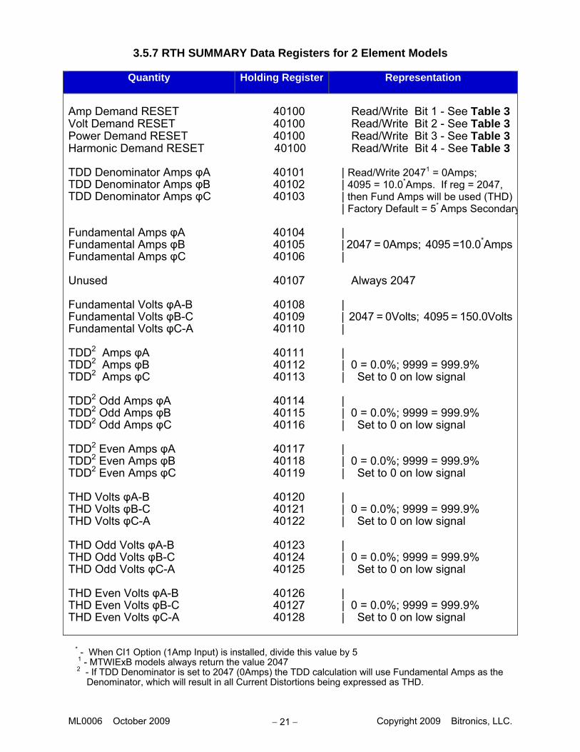
3.5.7 RTH SUMMARY Data Registers for 2 Element Models
Quantity Holding Register Representation
Amp Demand RESET 40100 Read/Write Bit 1 - See Table 3 Volt Demand RESET 40100 Read/Write Bit 2 - See Table 3 Power Demand RESET 40100 Read/Write Bit 3 - See Table 3 Harmonic Demand RESET 40100 Read/Write Bit 4 - See Table 3 TDD Denominator Amps φA 40101 | Read/Write 20471 = 0Amps; TDD Denominator Amps φB 40102 | 4095 = 10.0*Amps. If reg = 2047, TDD Denominator Amps φC 40103 | then Fund Amps will be used (THD)
| Factory Default = 5* Amps Secondary Fundamental Amps φA 40104 | Fundamental Amps φB 40105 | 2047 = 0Amps; 4095 =10.0*AmpsFundamental Amps φC 40106 | Unused 40107 Always 2047 Fundamental Volts φA-B 40108 | Fundamental Volts φB-C 40109 | 2047 = 0Volts; 4095 = 150.0VoltsFundamental Volts φC-A 40110 | TDD2 Amps φA 40111 | TDD2 Amps φB 40112 | 0 = 0.0%; 9999 = 999.9% TDD2 Amps φC 40113 | Set to 0 on low signal TDD2 Odd Amps φA 40114 | TDD2 Odd Amps φB 40115 | 0 = 0.0%; 9999 = 999.9% TDD2 Odd Amps φC 40116 | Set to 0 on low signal TDD2 Even Amps φA 40117 | TDD2 Even Amps φB 40118 | 0 = 0.0%; 9999 = 999.9% TDD2 Even Amps φC 40119 | Set to 0 on low signal THD Volts φA-B 40120 | THD Volts φB-C 40121 | 0 = 0.0%; 9999 = 999.9% THD Volts φC-A 40122 | Set to 0 on low signal THD Odd Volts φA-B 40123 | THD Odd Volts φB-C 40124 | 0 = 0.0%; 9999 = 999.9% THD Odd Volts φC-A 40125 | Set to 0 on low signal THD Even Volts φA-B 40126 | THD Even Volts φB-C 40127 | 0 = 0.0%; 9999 = 999.9% THD Even Volts φC-A 40128 | Set to 0 on low signal * - When CI1 Option (1Amp Input) is installed, divide this value by 5 1 - MTWIExB models always return the value 2047 2 - If TDD Denominator is set to 2047 (0Amps) the TDD calculation will use Fundamental Amps as the Denominator, which will result in all Current Distortions being expressed as THD.

ML0006 October 2009 Copyright 2009 Bitronics, LLC. 22
3.5.7 RTH SUMMARY Data Registers for 2 Element Models (Cont’d)
Quantity Holding Register Representation
K-Factor Amps φA 40129 | K-Factor Amps φB 40130 | 100 = 1.00; 65,535 = 655.35 K-Factor Amps φC 40131 | Set to 100 on low signal Unused 40132 | Unused 40133 | Always 2047 Unused 40134 | Displacement PF Total 40135 1047 = -1; 2047 = 0; 3047 = +1
4046 = Amps or Volts too low (-) lagging; (+) leading
Unused 40136 | Unused 40137 | Always 2047 Present Demand TDD1 Amps φA 40138 | Present Demand TDD1 Amps φB 40139 | 0 = 0.0%; 9999 = 999.9% Present Demand TDD1 Amps φC 40140 | Max Demand TDD1 Amps φA 40141 | Max Demand TDD1 Amps φB 40142 | 0 = 0.0%; 9999 = 999.9% Max Demand TDD1 Amps φC 40143 | Present Demand THD Volts φA-B 40144 | Present Demand THD Volts φB-C 40145 | 0 = 0.0%; 9999 = 999.9% Present Demand THD Volts φC-A 40146 | Max Demand THD Volts φA-B 40147 | Max Demand THD Volts φB-C 40148 | 0 = 0.0%; 9999 = 999.9% Max Demand THD Volts φC-A 40149 | 1 If TDD Denominator is set to 2047 (0Amps) the TDD calculation will use Fundamental Amps as the Denominator, which will result in all Current Distortions being expressed as THD.

ML0006 October 2009 Copyright 2009 Bitronics, LLC. 23
3.5.8 RTH INDIVIDUAL Data Registers for 2 Element Models
Quantity Holding Register
Representation
φA Amps Distortion Denominator 40150 | 2047 = 0Amps; 4095 = 10.0*Amps
| =40101 if TDD, =40104 if THD φA Amps Demand Distortion1 - I1 40151 | φA Amps Demand Distortion1 - I2 40152 |
: : | 0 = 0.0%; 9999 = 999.9% : : | Set to 0 on low signal
φA Amps Demand Distortion1 - I30 40180 | φA Amps Demand Distortion1 - I31 40181 | φA-B Volts Distortion Denominator 40182 | 2047 = 0Volts; 4095 = 150.0Volts
| =40108 φA-B Volts Harm. Distortion - V1 40183 | φA-B Volts Harm. Distortion - V2 40184 |
: : | 0 = 0.0%; 9999 = 999.9% : : | Set to 0 on low signal
φA-B Volts Harm. Distortion - V30 40212 | φA-B Volts Harm. Distortion - V31 40213 | φB Amps Distortion Denominator 40214 | 2047 = 0Amps; 4095 = 10.0*Amps
| =40102 if TDD, =40105 if THD φB Amps Demand Distortion1 - I1 40215 | φB Amps Demand Distortion1 - I2 40216 |
: : | 0 = 0.0%; 9999 = 999.9% : : | Set to 0 on low signal
φB Amps Demand Distortion1 - I30 40244 | φB Amps Demand Distortion1 - I31 40245 | φB-C Volts Distortion Denominator 40246 | 2047 = 0Volts; 4095 = 150.0Volts
| =40109 φB-C Volts Harm. Distortion - V1 40247 | φB-C Volts Harm. Distortion - V2 40248 |
: : | 0 = 0.0%; 9999 = 999.9% : : | Set to 0 on low signal
φB-C Volts Harm. Distortion - V30 40276 | φB-C Volts Harm. Distortion - V31 40277 | * - When CT1 Option (1Amp Input) is installed, divide this value by 5 1 If TDD Denominator is set to 2047 (0Amps) the TDD calculation will use Fundamental Amps as the Denominator, which will result in all Current Distortions being expressed as THD.

ML0006 October 2009 Copyright 2009 Bitronics, LLC. 24
3.5.8 RTH INDIVIDUAL Data Registers for 2 Element Models (Cont’d)
Quantity Holding Register
Representation
φC Amps Distortion Denominator 40278 | 2047 = 0Amps; 4095 = 10.0*Amps
| =40103 if TDD, =40106 if THD φC Amps Demand Distortion1 - I1 40279 | φC Amps Demand Distortion1 - I2 40280 |
: : | 0 = 0.0%; 9999 = 999.9% : : | Set to 0 on low signal
φC Amps Demand Distortion1 - I30 40308 | φC Amps Demand Distortion1 - I31 40309 | φC-A Volts Distortion Denominator 40310 | 2047 = 0Volts; 4095 = 150.0Volts
| =40110 φC-A Volts Harm. Distortion - V1 40311 | φC-A Volts Harm. Distortion - V2 40312 |
: : | 0 = 0.0%; 9999 = 999.9% : : | Set to 0 on low signal
φC-A Volts Harm. Distortion - V30 40340 | φC-A Volts Harm. Distortion - V31 40341 | * - When CT1 Option (1Amp Input) is installed, divide this value by 5 1 If TDD Denominator is set to 2047 (0Amps) the TDD calculation will use Fundamental Amps as the Denominator, which will result in all Current Distortions being expressed as THD.

ML0006 October 2009 Copyright 2009 Bitronics, LLC. 25
3.6 Writeable Registers 3.6.1 Setting CT and PT Ratios The MultiComm instrument is capable of internally storing and recalling CT and PT ratios via the network interface, or through the internal toggle/push-button (Refer to Section 4.1 of the MultiComm User Manual). These ratios are used to scale the display values in engineering (primary) units. These ratios are also used to scale the Energy quantities, registers 40019 through 40026 (Refer to Section 3.5 for register assignments) which are also in primary units. When the CT and PT ratios are set, they are written to registers 40041 through 40044, and are stored in non-volatile memory on the CT/PT Board. Each ratio is stored in two registers, one for the normalized format ratio, and the other for the divisor. Allowable constants for CT Value (40041) are 500 to 9999, and 1000 to 9999 for PT Value (40043). The divisors may be 1, 10, 100, or 1000 only. The number stored will be the high side rating of the CT. A 500:5 ratio CT will have a value of 500 stored, while a 100:1 CT will have a value of 100 stored. For example, to calculate a CT ratio from the data stored in the MultiComm, use the following equation:
The CT and PT ratios values may be used with the equations in Section 3.5 or 3.7 to derive primary unit quantities from the MultiComm. For example, the equation for amperes becomes:
The values stored in registers 40041 and 40043 are duplicated in registers 40016 and 40017 respectively. Registers 40016 and 40017 are READ ONLY and cannot be written to. In the event of a CT/PT Ratio Checksum Failure, the value in the CT Ratio and PT Ratio registers default to 65535 (FFFF Hex), and the value in the CT Ratio Divisor and PT Ratio Divisor default to 0001. See Section 3.8 for more details.
WARNING - THE RATIO NON-VOLATILE MEMORY STORAGE HAS A 1,000,000 CYCLE ENDURANCE (RATIOS CAN BE CHANGED 1,000,000 TIMES). ONLY WRITE TO RATIO REGISTERS WHEN THE RATIOS NEED TO BE CHANGED.
3.6.2 Resetting Energy and Demands The Energy and Demand registers can be RESET by writing a bit pattern to Holding Register 40100. Any "1" bits in the proper position cause initiation of the corresponding RESET. Multiple RESETs can be accomplished by using either multiple WRITE commands or a single WRITE command with multiple bits set. Table 3 shows the correspondence between the RESET functions and the bits set. The Registers will be reset
(40044) Divisor Ratio PT
(40043) Value PT = PT
SecondaryCT x (40042) Divisor Ratio CT
(40041) Value CT = CT
RATIO
RATIO
Ratio CT x Value ScaleFull x 2048
2047 - Value = AMPEREs

ML0006 October 2009 Copyright 2009 Bitronics, LLC. 26
within 0.6 seconds, however it may take the meter up to 10 seconds to clear the data stored in the EEPROM. The USER must ensure that the power is not interrupted to the meter for this 10 second period after this command is issued.
Bit
Position
Value
Description Registers Affected Global
0
1
Reset (ZERO) Energy 40019 .. 40026 19..26
1
2
Reset AMP Demands 40045 .. 40052, 40136,
40137 N/A
2
4
Reset Volt Demands 40053 .. 40061 N/A
3
8
Reset Power Demands 40062 .. 40070 N/A
4
16
Reset Harmonic Demands
40138 .. 40149 N/A
3.6.3 TDD Writeable Denominators The MultiComm instrument is capable of internally storing and recalling Current Values that are used as Denominators in determining the Total Demand Distortion (TDD). The denominator values are stored for each phase, and are stored in Registers 40101, 40102, 40103 for Phase A, Phase B, and Phase C respectively. These denominators affect all Current Harmonic Measurements (Refer to Section 3.5 for register assignments). The Denominators are written to registers 40101 through 40103 over the Modbus Plus communication port, and are stored in non-volatile memory on the Analog Board. The value that needs to be stored follows the same offset binary equation that is used with the other measurements. For a 5A secondary CT, the equation for amperes becomes: where Value is the Binary Value that should be stored in the denominator register, and Amperes is the actual value of primary current that the user intends for the TDD calculations. The factory default value is 3071 which corresponds to 5 Amps Secondary (1 Amp for CI1 option). If the value stored in the denominator register are set to Zero amps (Value = 2047), then the Harmonic Distortion calculations will use the Fundamental Magnitude of the current, which will result in the Distortion Values to be in the form of THD
instead of TDD. The values stored in registers 40101, 40102 and 40103 are duplicated in registers 40150, 40214 and 40278 respectively if the value are non-zero (TDD). If registers 40101,2,3 are set to zero (THD) then the registers 40150, 40214 and 40278 will contain the Magnitude of the Fundamental.
WARNING - THE DENOMINATOR NON-VOLATILE MEMORY STORAGE HAS A 1,000,000 CYCLE ENDURANCE (DENOMINATORS CAN BE CHANGED 1,000,000 TIMES). ONLY WRITE TO THE DENOMINATOR REGISTERS WHEN THE DENOMINATORS NEED TO BE CHANGED.
5 x Divisor Ratio CT
Value CT x 10 x
2048
2047 - Value = AMPEREs
ML0006 October 2009 Copyright 2009 Bitronics, LLC. 27
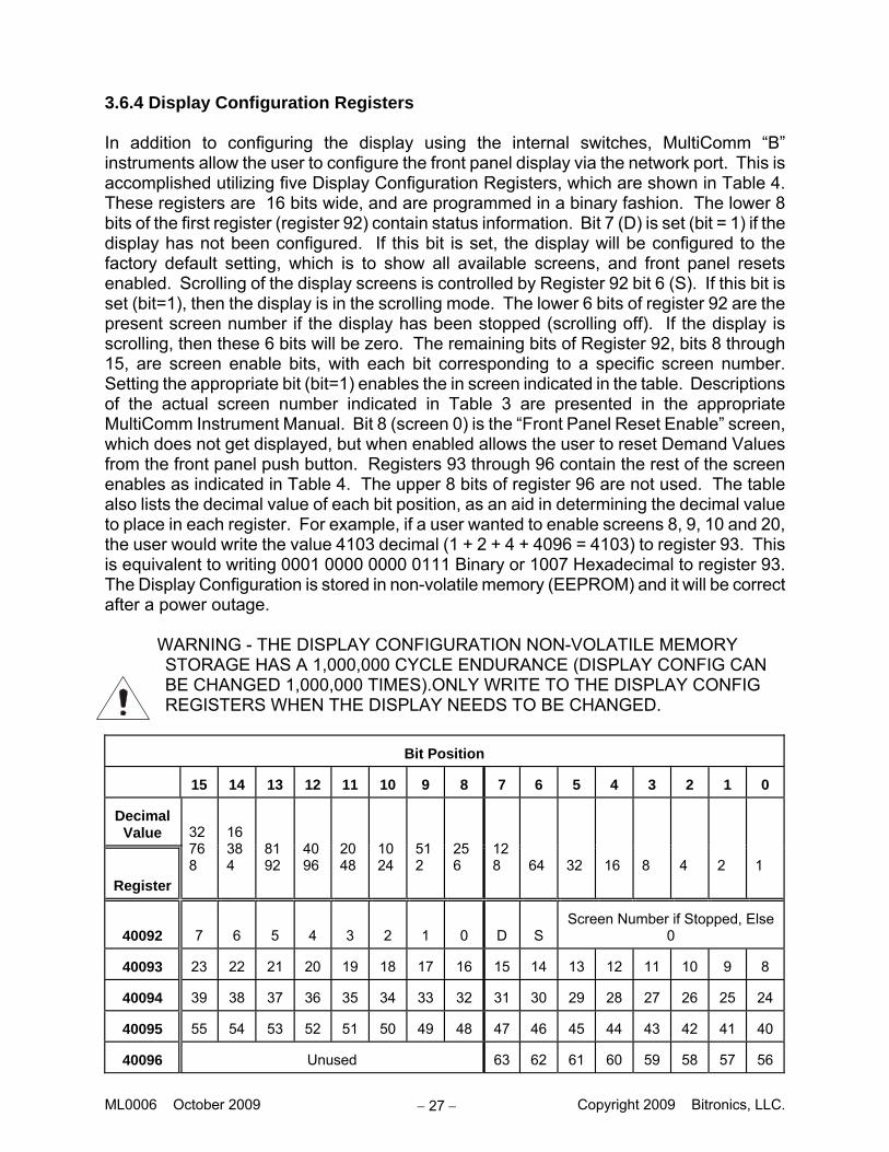
3.6.4 Display Configuration Registers In addition to configuring the display using the internal switches, MultiComm “B” instruments allow the user to configure the front panel display via the network port. This is accomplished utilizing five Display Configuration Registers, which are shown in Table 4. These registers are 16 bits wide, and are programmed in a binary fashion. The lower 8 bits of the first register (register 92) contain status information. Bit 7 (D) is set (bit = 1) if the display has not been configured. If this bit is set, the display will be configured to the factory default setting, which is to show all available screens, and front panel resets enabled. Scrolling of the display screens is controlled by Register 92 bit 6 (S). If this bit is set (bit=1), then the display is in the scrolling mode. The lower 6 bits of register 92 are the present screen number if the display has been stopped (scrolling off). If the display is scrolling, then these 6 bits will be zero. The remaining bits of Register 92, bits 8 through 15, are screen enable bits, with each bit corresponding to a specific screen number. Setting the appropriate bit (bit=1) enables the in screen indicated in the table. Descriptions of the actual screen number indicated in Table 3 are presented in the appropriate MultiComm Instrument Manual. Bit 8 (screen 0) is the “Front Panel Reset Enable” screen, which does not get displayed, but when enabled allows the user to reset Demand Values from the front panel push button. Registers 93 through 96 contain the rest of the screen enables as indicated in Table 4. The upper 8 bits of register 96 are not used. The table also lists the decimal value of each bit position, as an aid in determining the decimal value to place in each register. For example, if a user wanted to enable screens 8, 9, 10 and 20, the user would write the value 4103 decimal (1 + 2 + 4 + 4096 = 4103) to register 93. This is equivalent to writing 0001 0000 0000 0111 Binary or 1007 Hexadecimal to register 93. The Display Configuration is stored in non-volatile memory (EEPROM) and it will be correct after a power outage.
WARNING - THE DISPLAY CONFIGURATION NON-VOLATILE MEMORY STORAGE HAS A 1,000,000 CYCLE ENDURANCE (DISPLAY CONFIG CAN BE CHANGED 1,000,000 TIMES).ONLY WRITE TO THE DISPLAY CONFIG REGISTERS WHEN THE DISPLAY NEEDS TO BE CHANGED.
Bit Position
15
14
13
12
11 10 9 8 7 6 5 4
3
2 1 0
Decimal
Value
32768
16384
8192
4096
2048
1024
512
256
128
64
32
16
8
4
2
1
Register
40092
7
6
5
4
3
2
1
0
D
S
Screen Number if Stopped, Else 0
40093
23
22
21
20
19 18 17 16 15 14 13 12
11
10 9 8
40094
39
38
37
36
35 34 33 32 31 30 29 28
27
26 25 24
40095
55
54
53
52
51 50 49 48 47 46 45 44
43
42 41 40
40096
Unused 63 62 61 60
59
58 57 56

ML0006 October 2009 Copyright 2009 Bitronics, LLC. 28
3.6.5 Communication Configuration Registers MultiComm “B” instruments provide READ/WRITE Communication Configuration Registers that allow the user to configure various parameters within the instrument. These Communication Configuration Registers are currently undefined for Modbus Plus, and will always return 0, however they are stored in non-volatile memory (EEPROM) to allow for future upgrades.
WARNING - THE COMMUNICATION CONFIGURATION NON-VOLATILE MEMORY STORAGE HAS A 1,000,000 CYCLE ENDURANCE (CONFIG CAN BE CHANGED 1,000,000 TIMES). ONLY WRITE TO THE CONFIGURATION REGISTERS WHEN THE CONFIGURATION NEEDS TO BE CHANGED.
3.6.6 Tag Register MultiComm “B” instruments provide a “TAG” register for user identification purposes. This register is READ/WRITE register that allows the user to write a number from 1 to 32,767 in the tag register. The Instrument will write this value in non-volatile memory EEPROM, so that the value will be available after any power outage. Any attempts to write values above 32,767 will return an illegal value error. Units will be set to 0 from the factory.
WARNING - THE TAG REGISTER NON-VOLATILE MEMORY STORAGE HAS A 1,000,000 CYCLE ENDURANCE (THE TAG REGISTER CAN BE CHANGED 1,000,000 TIMES). ONLY WRITE TO THE TAG REGISTER WHEN THE TAG NEEDS TO BE CHANGED.
3.7 Converting Data to Engineering Units As was mentioned in Section 3.5, the majority of the data in both the Global and Holding Registers is stored in a 12-BIT OFFSET BINARY format. This format was chosen to allow efficient use of registers, since both positive and negative quantities can be transmitted without the use of a SIGN (polarity) register. In this format, ZERO (0) is represented as 2047 counts, the most negative number is represented by 0 counts and the most positive number is represented by 4095 counts. While it would appear that this format limits the ACCURACY of the values transmitted in the registers, the RESOLUTION of this method is one part in 2048 which is 0.05%, actually 5 times better than the rated accuracy of the instrument, and therefore has no measurable effect on the accuracy of the transmitted value. When displaying these values at another location, it may be desirable to convert the offset binary format into ENGINEERING UNITS. This conversion is readily accomplished using the following simple scaling equations: BASIC EQUATION FOR OFFSET BINARY:
Ratio x Scale Full x 2048
2047 - Value = Units gEngineerin SECONDARY

ML0006 October 2009 Copyright 2009 Bitronics, LLC. 29
The CT and PT ratios are the NAMEPLATE ratings of the transducer transformers. The PT ratio in these equations is the same as the PT ratio stored in the transducer since convention is to specify the PT ratio as a ratio to 1. For 5Amp CTs, the CT ratio in these equations is not the same as the ratio stored in the meter, but rather the number stored in the meter divided by 5. This is due to the fact that 5Amp CT ratios are normally specified as a ratio to 5. For 1Amp Cts, the CT ratio is the same as that stored in the instrument. Refer to Section 3.6.1 for more information on the CT/PT Ratios. For example a 500:5 CT and a 4:1 PT would have the following ratios:
The Value referred to in the equations would be the value stored in the register that you wished to convert to engineering units. For example if you wanted to convert Phase A Amperes into engineering units, Value would be the value in Holding Register 40002. The ENERGY Registers are stored in the BIN8 format, making these values readily usable with the standard Double Precision Integer Math functions available on PLCs. Using this data format, the address specifying the WORD (both registers) is the address of the first of the two registers in the pair (i.e. the one with the lowest register number). This register will have the most significant portion of the number. If the BIN8 data format is specified, no conversion is required. FREQUENCY is stored as a single binary value that is the actual frequency times 100. PHASE is stored as an offset binary value that is the phase difference times 10. THD and TDD are stored as a single binary value that is the actual THD or TDD times 10. K FACTOR is stored as a single binary value that is the actual K Factor times 100.
4 = 1
4 = 1:4 = PT 100 =
5
500 = 5:500 = CT RATIORATIO

ML0006 October 2009 Copyright 2009 Bitronics, LLC.
30
2 ½ or 3 ELEMENT EQUATIONS:
5by value this divide Option, CT1 For* 100
Value = FACTOR K
10
Value = TDD THD,
Ref) Leading Line + ( 10
2047 - Value = DIFFERENCE PHASE
) Lead + ,Lag - ( 1000
2047 - Value = PF
100
Value = FREQUENCY
Value + 10,000 x Value = (kVARh) kWh
CT x PT x 1000 x 2048
2047 - Value = )(VAs (VARs) WATTs
CT x PT x 3000 x 2048
2047 - Value = )(VAs (VARs) WATTs
3 x PT x 150 x 2048
2047 - Value = (SCALED) VOLTs
PT x 150 x 2048
2047 - Value = VOLTs
CT x 15 x 2048
2047 - Value= AMPEREs
CT x 10 x 2048
2047 - Value = AMPEREs
) Demand, Inst, Volts, (Amps,
nt)Displaceme (True,
LOWHIGH
RATIORATIO*
(Inst) PHASE PER
RATIORATIO*
) , Demand, (Inst, TOTAL
RATIO) , Demand, (Inst, L-L
RATIO) , Demand, Fund, (Inst, N-L
RATIO*
) Demand, Fund, (Inst, N
RATIO*
) Demand, Fund, (Inst,
Max
MaxMin
MaxMin
MaxMin
Max
Max
ML0006 October 2009 Copyright 2009 Bitronics, LLC.
31
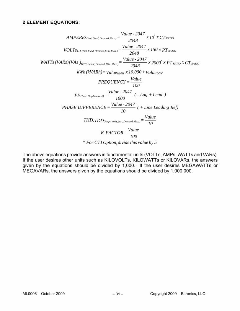
2 ELEMENT EQUATIONS:
The above equations provide answers in fundamental units (VOLTs, AMPs, WATTs and VARs). If the user desires other units such as KILOVOLTs, KILOWATTs or KILOVARs, the answers given by the equations should be divided by 1,000. If the user desires MEGAWATTs or MEGAVARs, the answers given by the equations should be divided by 1,000,000.
5by value this divide Option, CT1 For* 100
Value = FACTOR K
10
Value = TDD THD,
Ref) Leading Line + ( 10
2047 - Value = DIFFERENCE PHASE
) Lead + Lag, - ( 1000
2047 - Value = PF
100
Value = FREQUENCY
Value + 10,000 x Value = (kVARh) kWh
CT x PT x 2000 x 2048
2047 - Value = )(VAs (VARs) WATTs
PT x 150 x 2048
2047 - Value = VOLTs
CT x 10 x 2048
2047 - Value = AMPEREs
) Demand, Inst, Volts, (Amps,
nt)Displaceme (True,
LOWHIGH
RATIORATIO*
) , Demand, (Inst, TOTAL
RATIO) , Demand, Fund, (Inst, L-L
RATIO*
) Demand, Fund, (Inst,
Max
MaxMin
MaxMin
Max

ML0006 October 2009 Copyright 2009 Bitronics, LLC. 32
3.8 Health Check The following information is contained in the Health Check register (bit 15 is the high order bit and the description indicates the meaning when the bit is set). The Health Check Register should always be read and checked before interpreting data, since some failure modes will cause erroneous data to be presented. Please consult Table I in the base instrument MultiComm Users Manual for a full description of the failures.
BIT DESCRIPTION Self Test Fault Display Code
0 CT/PT Ratio Checksum Failure 4 2 ---1 1 CT/PT Board Calibration Checksum Failure 5 3 ---2 2 Analog Board Calibration Checksum Failure 2 4 ---3 3 Input Over-Range (Clipping) 6 6 ---4 4 Program Memory (EPROM) Failure 7 7 ---5 5 A/D Self-Test Error 4 8 ---6 6 External Memory (XRAM) Failure 4 9 ---7 7 Host-MultiComm Interface Crash 10 ---8 8 Phase Calibration Checksum Failure 8 N/A N/A 9 Energy Storage Checksum Failure 9 11 ---9 10 Demand Storage Parity Error 10 12 --10 11 Configuration Parity Error 13 --11 12 Future Expansion - will read 0 13 Future Expansion - will read 0 14 Future Expansion - will read 0 15 Will Always Read 0
4 - All measurements except energy are accurate, CT & PT ratio may be corrupted, no display on instrument. All Energies calculated after the failure will be in secondary units ( CTR = 5:5 & PTR = 1:1).
5 - Accuracy of measurements reduced to +/-3% or better.
6 - Accuracy of measurements reduced - dependent on amount of signal overrange.
7 - Data may be corrupted and is unreliable.
8 - Accuracy of WATT/VAR/Energy measurements reduced to +/-0.5% or better.
9 - Stored Energy Data may be corrupted and may be unreliable.
10 - Minimum and Maximum Demand Data may be corrupted. Present Demands unaffected.

ML0006 October 2009 Copyright 2009 Bitronics, LLC. 33
3.9 Modbus Plus Diagnostic LED The Modbus Plus Diagnostic LED is an indicator that shows the type of communications activity on the Modbus Plus port on the MultiComm instrument. The Diagnostic LED is a red indicator that is located in the upper left corner of the top display. Because the LED is actually on the board below the Display Board, the Diagnostic LED has a limited viewing angle. A specific flash pattern indicates the nature of the Modbus Plus communication activity as listed below:
Six flashes per second: The normal operating state for a Modbus Plus node. The node is successfully receiving and passing the token. All nodes on the network should be flashing this pattern.
One flash per second: The node is offline after just being powered up, or after hearing a message from another node with the same address (duplicate addresses are not allowed). In this state, the node monitors the network and builds a table of active nodes and token-holding nodes. It remains in this state for five seconds, then attempts to go to its normal operating state.
Two flashes, then OFF for two seconds: The node is hearing the token being passed among other nodes, but is never receiving the token. Check the network link for an open or short circuit, or for a defective termination. Check that the flexible circuit connector inside the MultiComm instrument is correctly seated.
Three flashes, then OFF for 1.7 seconds: The node is not hearing any other nodes. It is periodically claiming the token, but finding no other node to which to pass it. Check the network link for an open or short circuit, or for a defective termination. Check that the flexible circuit connector inside the MultiComm instrument is correctly seated.
Four flashes, then OFF for 1.4 seconds: The node has heard a valid message from another node that is using the same address as this node. The node remains offline in this state as long as it continues to hear the duplicate address. If the duplicate address is not heard for five seconds, the node then changes to the pattern of one flash every second.
3.10 Heartbeat State Counter MultiComm “B” instruments provide a Heartbeat State Counter Register that allows the user to determine when the data is updated within the instrument. For Modbus Plus this counter is also available in Global Data. This counter will increment by the number of internal 10 millisecond states that have elapsed since the last time the data was updated. Users can use a change in this value as an indication of the instant that the data has been updated in the MultiComm processor. On sequential polls, users can also use the difference in this counter to determine the time that has elapsed between poles. A third use of this register as a visual indicator that the data is changing, allows users of certain MMIs to identify disruption in the polling of the instrument. The Heartbeat State Counter is a full 16bit counter that rolls over at 65535 (655.35 seconds - 10.9225 minutes). The counter starts at zero on power-up, and is NOT stored in non-volatile memory.

ML0006 October 2009 Copyright 2009 Bitronics, LLC. 34
Model ID Model ID MTWIE1B 20
1 MTWDE1B 30
1 MTWIE2B 20
2 MTWDE2B 30
2 MTWIE3B 20
3 MTWDE3B 30
3 MTWIE4B 20
4 MTWDE4B 30
4 MTWIE5B 20
5 MTWDE5B 30
5 MTWIE6B 20
6 MTWDE6B 30
6 MTWIEC1B - VI3 20
7 MTWDEC1B - VI3 30
7 MTWIEC2B - VI2 20
8 MTWDEC2B - VI2 30
8 MTWIEC2B - VI4 20
9 MTWDEC2B - VI4 30
9 MTWIEC4B - VI3 21
0 MTWDEC4B - VI3 31
0 MTWIEC5B - VI2 21
1 MTWDEC5B - VI2 31
1 MTWIEC5B - VI4 21
2 MTWDEC5B - VI4 31
2
3.11 Meter ID Register MultiComm “B” instruments provide an “ID” register for model identification purposes. This register is preprogrammed at the factory, refer to table 5.

ML0006 October 2009 Copyright 2009 Bitronics, LLC. 35
4.0 INSTALLATION 4.1 Setting Modbus Plus Address The MultiComm instrument provides for direct connection to a Modbus Plus Network. As was mentioned in Section 3.3, each device on a given network must have a different PHYSICAL ADDRESS. A pair of address selector switches (SW3 & SW4) are located on the Modbus Plus Peer Processor Board, and they are accessible through holes in the Display Board. When the meter is powered, the ADDRESS can be easily checked by pressing the front mounted SELECT button down and scrolling through the available screens ( refer to the MultiComm Users Manual for more details on the screens). After all the screens have been viewed, a marker screen (CT/ID/PT shown below) will be displayed for 1.2 seconds.
5000 CT Ratio (5000:5 shown)(5000:1 with CT1 option) 12 ID Address (12 shown) 1000 PT Ratio (1000:1 shown) CTIDPT
This screen serves two purposes - to indicate to the user that all enabled screens have been viewed and to provide the CT/ID/PT information. The Modbus Plus Address is on the middle display. This provides the user with a simple method verifying the address without having to remove the faceplate of the instrument. If the ADDRESS needs to be changed, the following procedure should be followed:
1. With the MultiComm meter under power, remove the four screws holding the front panel to the meter. Carefully move the front panel away from the instrument to expose the front panel select switch, and disconnect the connector from the display board. Remove the faceplate and gasket.
2. Flip the small toggle switch on the left of the meter UP for CT set (DOWN for PT set). The top display will show the present CT setting, the middle display will show the instrument address and the bottom display will show the present PT setting. The Alphanumeric display will indicate which ratio is being set. Be careful not to push the Select button at this time or the CT\PT ratio will be altered.
3. Return the toggle to the center position. The alphanumeric display will show a Select? prompt for 2 seconds. If the Select button is pressed during the time, the alphanumeric display will indicate Okay, and the user will enter the Display Programming Mode. If the select button is not pressed, the Select? prompt will be followed by a digit check (8888 displayed) and the meter will return to normal operation. 4. The ADDRESS selector switches are SW3 & SW4, and are located on the right hand side of the Display Board, just below the SELECT pushbutton. The switches have 16 positions (0-9,A-F). The switch can be rotated with a small flat blade screwdriver, or a small phillips screwdriver. Using the table on the next page, find the desired MODBUS PLUS address and dial the switches SW4 and SW3 to the

ML0006 October 2009 Copyright 2009 Bitronics, LLC. 36
corresponding hexadecimal values. The NEW address will NOT take effect until the instrument has gone through its power-on functions.

ML0006 October 2009 Copyright 2009 Bitronics, LLC. 37
This can be accomplished by re-powering the instrument. For installed instruments where re-powering is not practical, the user may force the instrument into the power up sequence. To accomplish this, the CT/PT toggle should be moved from the center position to the up position. Then the user should PRESS and HOLD the SELECT button down for longer than 1.2 seconds, which will initiate a restart of the instrument. Return the toggle to the center position. You will see a digit check (8888 displayed).
5. Flip the small toggle switch on the left of the meter UP for CT set (DOWN for PT set). The top display will show the present CT setting, the middle display will show the instrument address and the bottom display will show the present PT setting. The Alphanumeric display will indicate which ratio is being set. Be careful not to push the Select button at this time or the CT\PT ratio will be altered. Verify that both ratios and the Modbus Plus Address are correct. Return the toggle to the center position. If the Modbus Plus Address is not correct, repeat step 4. If the CT and/or PT ratio have changed, refer to the MultiComm Users Manual for instructions on setting the CT/PT.
6. Replace gasket, carefully plug in the select switch connector to the two pin connector on the right hand side of the display board. Replace the front cover, being careful to dress the yellow cable to the select switch around the bottom display. Replace the four cover screws. Done!!
MB+
ADDR
SW4
SW3
MB+
ADDR SW4
SW3
MB+ ADDR
SW4
SW3
MB+
ADDR SW4
SW3
1
0
0
17 1 0 33 2 0
49 3 0
2
0
1
18 1 1 34 2 1
50 3 1
3
0
2
19 1 2 35 2 2
51 3 2
4
0
3
20 1 3 36 2 3
52 3 3
5
0
4
21 1 4 37 2 4
53 3 4
6
0
5
22 1 5 38 2 5
54 3 5
7
0
6
23 1 6 39 2 6
55 3 6
8
0
7
24 1 7 40 2 7
56 3 7
9
0
8
25 1 8 41 2 8
57 3 8
10
0
9
26 1 9 42 2 9
58 3 9
11
0
A
27 1 A 43 2 A
59 3 A
12
0
B
28 1 B 44 2 B
60 3 B
13
0
C
29 1 C 45 2 C
61 3 C
14
0
D
30 1 D 46 2 D
62 3 D
15
0
E
31 1 E 47 2 E
63 3 E
16
0
F
32 1 F 48 2 F
64 3 F

ML0006 October 2009 Copyright 2009 Bitronics, LLC. 38
4.2 Modbus Plus Cable The Modbus Plus cable connects to the MultiComm instrument via a standard 9-pin D connector located on the back of the instrument. Modicon recommends Belden 9841 cable or equivalent. The instrument is designed to accept standard Modicon Modbus Plus Connectors. The cable should enter the connector from the side with 4 pins, i.e. the narrow side. If the user is employing the Modicon Connector Tool (AS-MBPL-001), the wires should be dressed the same as the Modicon 385/485. This cable dress will put the Modbus Plus Cable to the outside of the meter, and will minimize the interference between the cable and the input studs. The Modbus Plus Connector should be secured to the MultiComm instrument using #4-40 screws supplied with the Modicon Connector Kit. For additional details, request Modicon publication GM-MBPL-001 “Modicon Modbus Plus Network Planning and Installation Guide” directly from your local Modicon distributor.

ML0006 October 2009 Copyright 2009 Bitronics, LLC. 39

Bitronics LLC. 261 Brodhead Road, Bethlehem, PA. 18017 (610) 997-5100 Fax (610) 997-5450
www.novatechweb.com/bitronics
Revision Date Changes By A 01/30/2009 Update Bitronics Name, Logo E. Demicco B 08/09/09 Updated logos and cover page MarCom C