modeling of charge collection efficiency degradation in ... · three main types of effects: -...
TRANSCRIPT

120 June 2016, Loughborough; E. Vittone
Modeling of charge collection efficiency degradation in semiconductor devices induced by
MeV ion beam irradiation
Ettore VittonePhysics Department
University of Torino - Italy
220 June 2016, Loughborough; E. Vittone
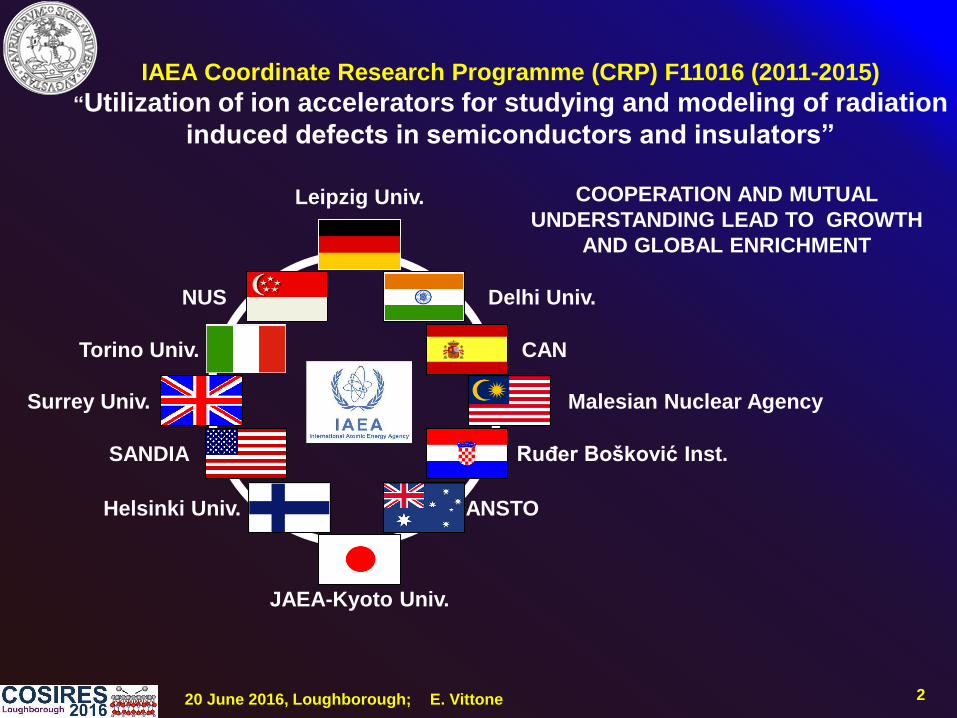
COOPERATION AND MUTUAL
UNDERSTANDING LEAD TO GROWTH
AND GLOBAL ENRICHMENT
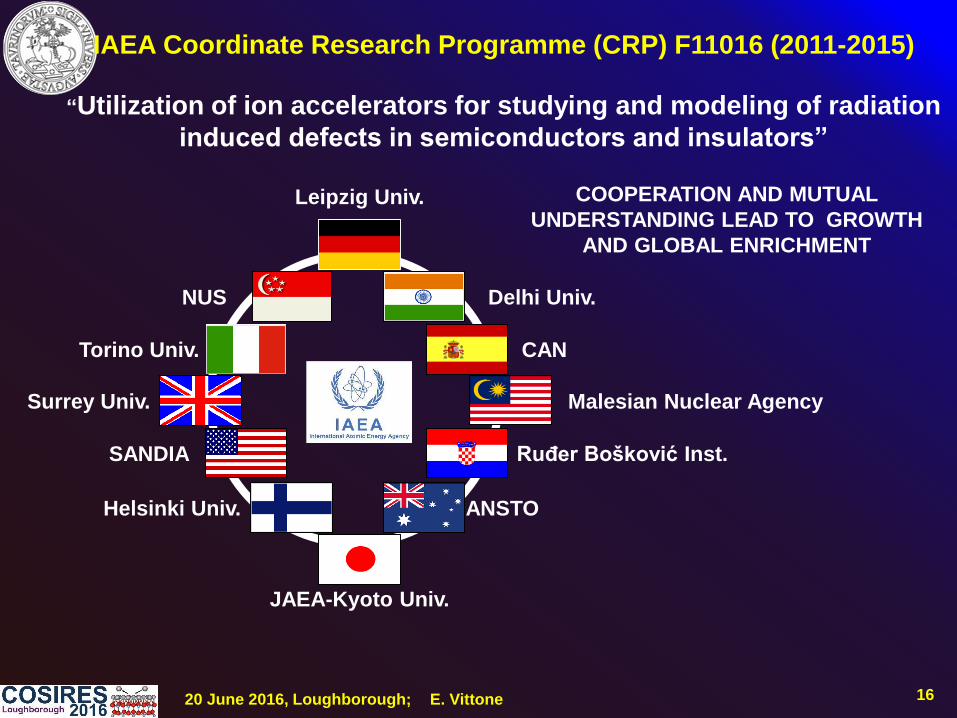
IAEA Coordinate Research Programme (CRP) F11016 (2011-2015)
“Utilization of ion accelerators for studying and modeling of radiation
induced defects in semiconductors and insulators”
NUS
Ruđer Bošković Inst.
Delhi Univ.
ANSTOHelsinki Univ.
CAN
JAEA-Kyoto Univ.
Malesian Nuclear Agency
Torino Univ.
Surrey Univ.
SANDIA
Leipzig Univ.
320 June 2016, Loughborough; E. Vittone
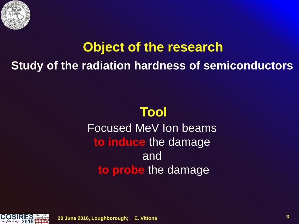
Object of the research
Study of the radiation hardness of semiconductors
ToolFocused MeV Ion beams
to induce the damage
and
to probe the damage

420 June 2016, Loughborough; E. Vittone
Radiation damage is the general alteration of the
operational properties of semiconductor devices induced
by ionizing radiation
Three main types of effects:
- Transient ionization. This effect produces electron-hole pairs; particle
detection with semiconductors is based on this effect.
-Long term ionization. In insulators (oxides), the material does not return to
its initial state, if the electrons and holes produced are fixed, and charged
regions are induced.
- Displacements. Dislocations of atoms from their normal
sites in the lattice, producing less ordered structures, with
long term effects on semiconductor properties.
520 June 2016, Loughborough; E. Vittone
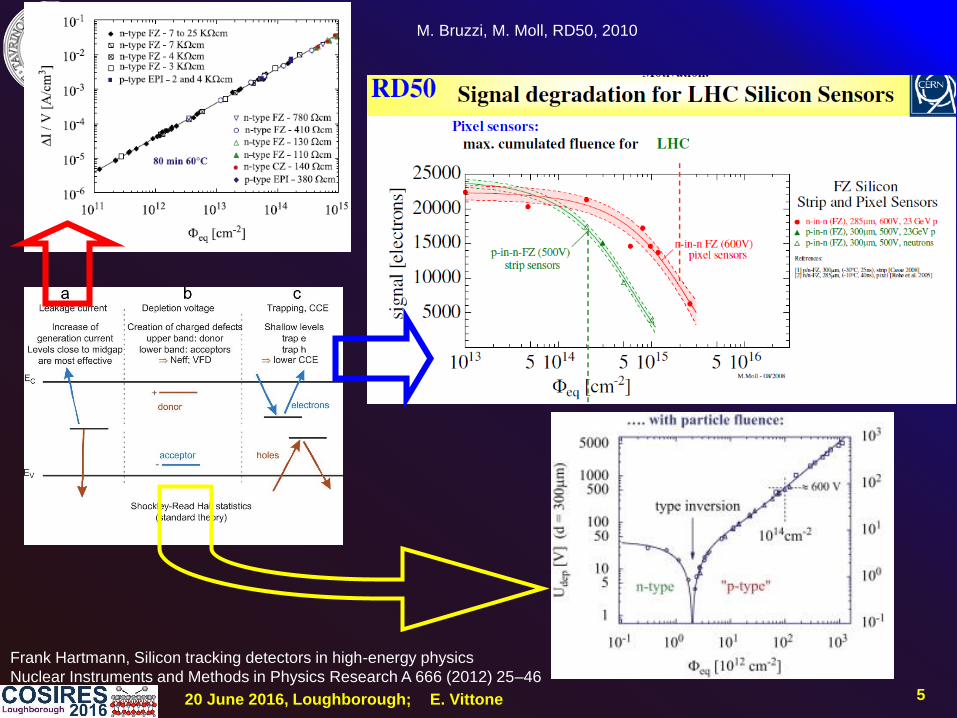
Frank Hartmann, Silicon tracking detectors in high-energy physics
Nuclear Instruments and Methods in Physics Research A 666 (2012) 25–46
M. Bruzzi, M. Moll, RD50, 2010
620 June 2016, Loughborough; E. Vittone
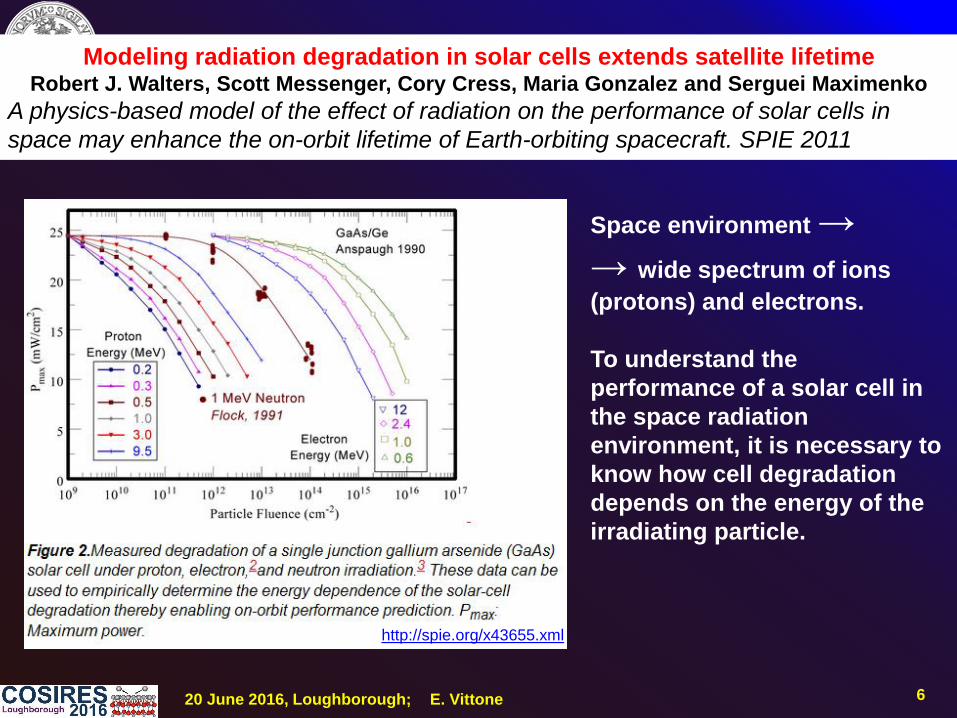
Modeling radiation degradation in solar cells extends satellite lifetimeRobert J. Walters, Scott Messenger, Cory Cress, Maria Gonzalez and Serguei Maximenko
A physics-based model of the effect of radiation on the performance of solar cells in
space may enhance the on-orbit lifetime of Earth-orbiting spacecraft. SPIE 2011
http://spie.org/x43655.xml
Space environment →
→ wide spectrum of ions
(protons) and electrons.
To understand the
performance of a solar cell in
the space radiation
environment, it is necessary to
know how cell degradation
depends on the energy of the
irradiating particle.

720 June 2016, Loughborough; E. Vittone
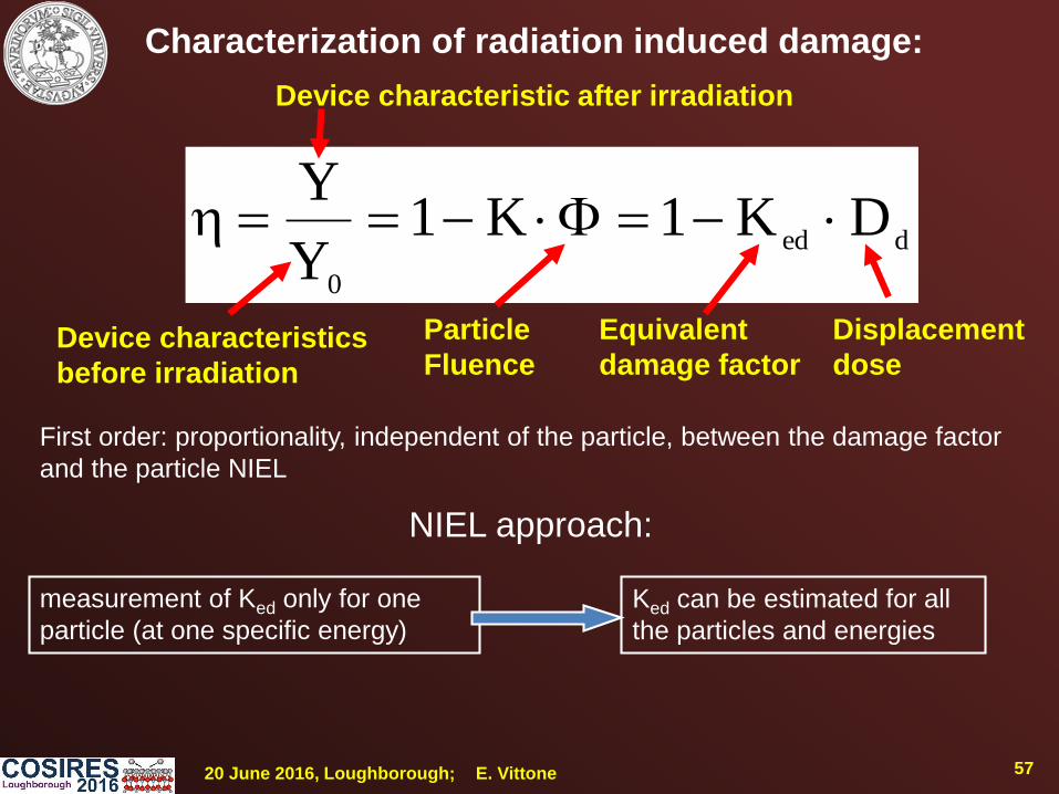
Characterization of radiation induced damage:
ded
0
DK1K1Y
Y
Device characteristics
before irradiation
Equivalent
damage factor
Particle
Fluence
Displacement
dose
Device characteristic after irradiation
First order: proportionality, independent of the particle, between the damage factor
and the particle NIEL
NIEL approach:
measurement of Ked only for one
particle (at one specific energy)
Ked can be estimated for all
the particles and energies

820 June 2016, Loughborough; E. Vittone
IBIC: Ion Beam Induced Charge
Transport)Carrier Free Energy, Deposited(FVout
Incoming radiation
V
Q
Incoming radiation
V
Vout
MeasuredWell known Material Characterization
Deposited Energy
Free charge generation
and transport
Output Electrical
Signal Vout
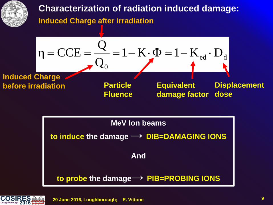
920 June 2016, Loughborough; E. Vittone
ded
0
DK1K1Q
QCCE
Induced Charge
before irradiation
Induced Charge after irradiation
Characterization of radiation induced damage:
Equivalent
damage factor
Particle
Fluence
Displacement
dose
MeV Ion beams
to induce the damage → DIB=DAMAGING IONS
And
to probe the damage→ PIB=PROBING IONS

1020 June 2016, Loughborough; E. Vittone
CCE degradationinduced by ion irradiation
1 10 100 1000
0,85
0,90
0,95
1,00
Cl 11 MeV
CC
E
Fluence (m-2)
Hamamatsu photodiode
Vbias = 100 V
Is a function of the damaging ion fluence
ded
0
DK1K1Y
Y
DIB= Cl 11 MeV
PIB= He 1.4 MeV
1120 June 2016, Loughborough; E. Vittone
1 10 100 1000
0,85
0,90
0,95
1,00
Cl 11 MeV
O 4 MeV
Li 2.15 MeV
CC
E
Fluence (m-2)
He 1.4 MeV
Hamamatsu photodiode
Vbias = 100 V
CCE degradationinduced by ion irradiation
Is a function of the ion energy and mass
ded
0
DK1K1Y
Y
PIB= He 1.4 MeV

1220 June 2016, Loughborough; E. Vittone
0,80
0,85
0,90
0,95
1,00
1 10 100 1000 10000
4H-SiC
Schottky diode
Hamamatsu
p-i-n diode
P-type Fz-Si
Fluence (m-2)
N-type Fz-Si
CC
ECCE degradation
induced by ion irradiationIs a function of the material and/or device
ded
0
DK1K1Y
Y

1320 June 2016, Loughborough; E. Vittone
10 100 1000
0,85
0,90
0,95
1,00
100 V
20 V
50 V
10 V
CC
E
Fluence (m-2)
He 1.4 MeV
Hamamatsu photodiode
Vbias = 100 V
Vbias
dedbias
0
DK1)V(K1Y
Y
CCE degradationinduced by ion irradiation
Is a function of the polarization state of the device
1420 June 2016, Loughborough; E. Vittone
100 1000 10000
0,3
0,4
0,5
0,6
0,7
0,8
0,9
1,0
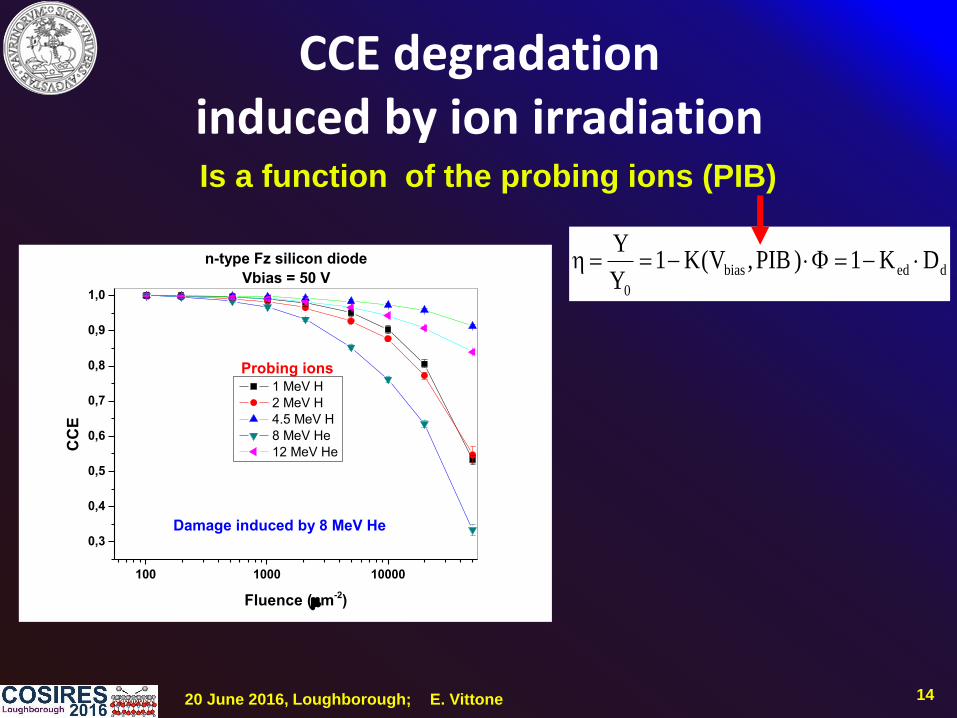
Damage induced by 8 MeV He
1 MeV H
2 MeV H
4.5 MeV H
8 MeV He
12 MeV HeCC
E
Fluence (m-2)
n-type Fz silicon diode
Vbias = 50 V
Probing ions
dedbias
0
DK1) PIB,V(K1Y
Y
CCE degradationinduced by ion irradiationIs a function of the probing ions (PIB)
1520 June 2016, Loughborough; E. Vittone
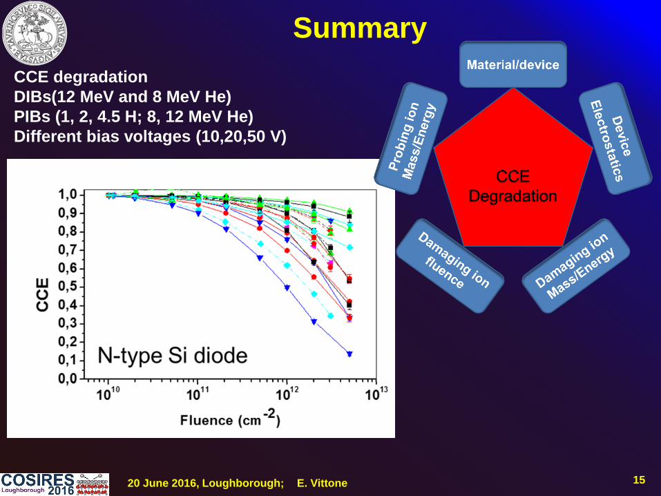
Summary
CCE degradation
DIBs(12 MeV and 8 MeV He)
PIBs (1, 2, 4.5 H; 8, 12 MeV He)
Different bias voltages (10,20,50 V)
1620 June 2016, Loughborough; E. Vittone
COOPERATION AND MUTUAL
UNDERSTANDING LEAD TO GROWTH
AND GLOBAL ENRICHMENT
IAEA Coordinate Research Programme (CRP) F11016 (2011-2015)
“Utilization of ion accelerators for studying and modeling of radiation
induced defects in semiconductors and insulators”
NUS
Ruđer Bošković Inst.
Delhi Univ.
ANSTOHelsinki Univ.
CAN
JAEA-Kyoto Univ.
Malesian Nuclear Agency
Torino Univ.
Surrey Univ.
SANDIA
Leipzig Univ.
1720 June 2016, Loughborough; E. Vittone
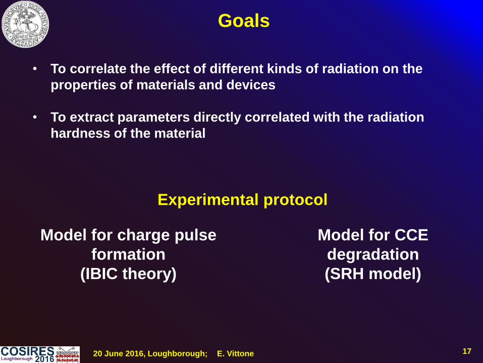
Model for charge pulse
formation
(IBIC theory)
Model for CCE
degradation
(SRH model)
Experimental protocol
• To correlate the effect of different kinds of radiation on the
properties of materials and devices
• To extract parameters directly correlated with the radiation
hardness of the material
Goals
1820 June 2016, Loughborough; E. Vittone
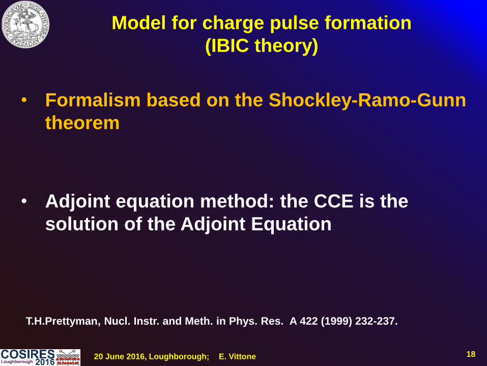
Model for charge pulse formation
(IBIC theory)
• Formalism based on the Shockley-Ramo-Gunn
theorem
• Adjoint equation method: the CCE is the
solution of the Adjoint Equation
T.H.Prettyman, Nucl. Instr. and Meth. in Phys. Res. A 422 (1999) 232-237.

1920 June 2016, Loughborough; E. Vittone
Gunn’s theorem
Pulse shapes calculation
V-qI
Ev
Shockley-Ramo theorem
d
1-qI v
Weighting field
Gunn theorem
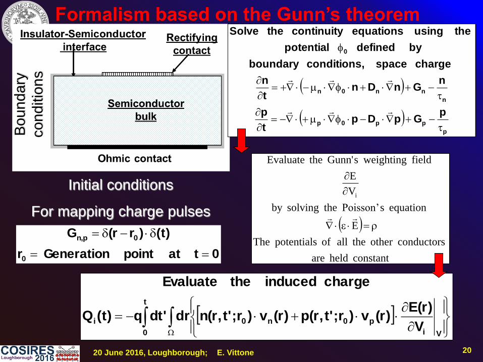
2020 June 2016, Loughborough; E. Vittone
Vi
p0n0
t
0
iV
)r(E)r(v)r;'t,r(p)r(v)r;'t,r(nrd'dtq)t(Q
charge induced the Evaluate
constant held are
conductorsother theall of potentials The
E
equation sPoisson’ thesolvingby
V
E
field g weightinsGunn' theEvaluate
i
Initial conditions
For mapping charge pulses
0tat point Generation r
)t()rr(G
0
0pn,
Formalism based on the Gunn’s theoremB
oun
da
ry
co
nd
itio
ns
p
pp0p
n
nn0n
0
pGpDp
t
p
nGnDn
t
n
charge space ,conditions boundary
by defined potential
the using equations continuity the Solve

2120 June 2016, Loughborough; E. Vittone
Model for charge pulse formation
(IBIC theory)
• Formalism based on the Shockley-Ramo-Gunn
theorem
• Adjoint equation method: the CCE is the
solution of the Adjoint Equation
T.H.Prettyman, Nucl. Instr. and Meth. in Phys. Res. A 422 (1999) 232-237.
2220 June 2016, Loughborough; E. Vittone
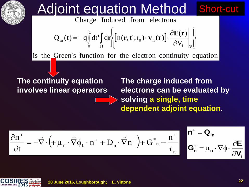
equation continuityelectron for thefunction sGreen' theis
V
)()()r;'t,(nd'dtq)t(Q
electrons from Induced Charge
Vi
n0
t
0
in
rErvrr
The continuity equation
involves linear operators
The charge induced from
electrons can be evaluated by
solving a single, time
dependent adjoint equation.
n
n*
n0n
nGnDn
t
n
i
nn
in
V
EG
Qn
Short-cutAdjoint equation Method

2320 June 2016, Loughborough; E. Vittone
d
0x
0
x
y nnS
d
x
y
x ppS
S
v
1dzexp
V
yFdy
v
1dzexp
V
yFdy
xdxqQ
Electrons
Holes
Gunn’s
weighting field
Drift lengths
Model for charge pulse formation
(IBIC theory)
Ionization profile Fully depleted device
No diffusion
Ramo Theorem
1D

2420 June 2016, Loughborough; E. Vittone
Capture
coefficient
)x(Vac11
0
Basic assumption:
1) In the linear regime, the ion induced damage affects mainly the carrier lifetime
2) The ion induced trap density is proportional to the VACANCY DENSITY
Fluence
Vacancy Density Profile
Model for CCE degradation
Shockley-Read-Hall model
2520 June 2016, Loughborough; E. Vittone
The experimental protocol
Z. Pastuovic et al., IEEE Trans on Nucl. Sc. 56 (2009) 2457; APL (98) 092101 (2011)

2620 June 2016, Loughborough; E. Vittone
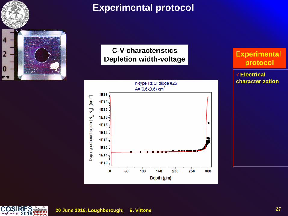
Samples under studyn- and p- type Fz p-i-n Si diodes
Fabricated by the Institute of Physics, University of Helsinki
16 floating guard rings
The frontal electrode and the guard rings
are coated with Al (0.5 µm]).
The Al electrode has a hole in the center, 1 mm diameter.
Different dimensions: 5 or 2.5 mm
MeV ions
2720 June 2016, Loughborough; E. Vittone
Electrical
characterization
C-V characteristics
Depletion width-voltageExperimental
protocol
Experimental protocol
2820 June 2016, Loughborough; E. Vittone
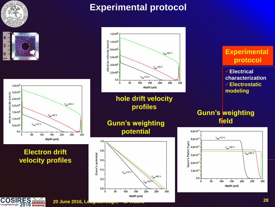
Electrical
characterization
Electrostatic
modeling
Experimental
protocol
Experimental protocol
Electron drift
velocity profiles
hole drift velocity
profiles
Gunn’s weighting
potential
Gunn’s weighting
field
2920 June 2016, Loughborough; E. Vittone
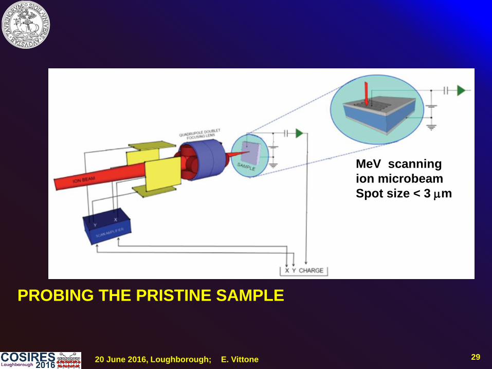
MeV scanning
ion microbeam
Spot size < 3 m
PROBING THE PRISTINE SAMPLE
3020 June 2016, Loughborough; E. Vittone
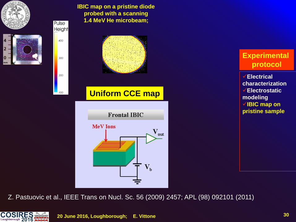
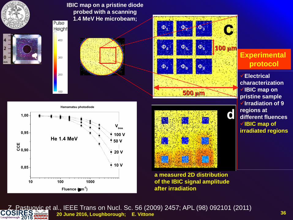
IBIC map on a pristine diode
probed with a scanning
1.4 MeV He microbeam;
Uniform CCE map
Electrical
characterization
Electrostatic
modeling
IBIC map on
pristine sample
Experimental
protocol
Z. Pastuovic et al., IEEE Trans on Nucl. Sc. 56 (2009) 2457; APL (98) 092101 (2011)

3120 June 2016, Loughborough; E. Vittone
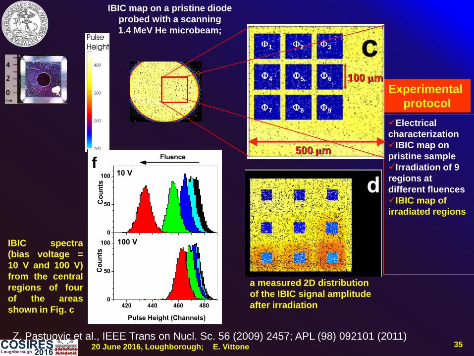
Ion microbeams
Different ion mass/energy
Spot size < 3 m
DAMAGING SELECTED AREAS
100X100 m2

3220 June 2016, Loughborough; E. Vittone
500 m
100 m
1 2
4 5
7 8
3
6
9
Electrical
characterization
IBIC map on
pristine sample
Irradiation of 9
regions at
different fluences
Experimental
protocol
Z. Pastuovic et al., IEEE Trans on Nucl. Sc. 56 (2009) 2457; APL (98) 092101 (2011)
IBIC map on a pristine diode
probed with a scanning
1.4 MeV He microbeam;
ZOOM in view of the selected area for focused
ion beam irradiation at different fluences
3320 June 2016, Loughborough; E. Vittone
He ion microbeam
Energy 1.4 MeV
Spot size < 3 m
0 1 2 3 4 5 6 70.0
0.1
0.2
0.3
Depth (m)
No
rmali
zed
Io
niz
ing
En
erg
y l
oss (
1/
m)
Data from SRIM
1.4 MeV He in Si
PROBING DAMAGED AREAS

3420 June 2016, Loughborough; E. Vittone
a measured 2D distribution
of the IBIC signal amplitude
after irradiation
Electrical
characterization
IBIC map on
pristine sample
Irradiation of 9
regions at
different fluences
IBIC map of
irradiated regions
Experimental
protocol
Z. Pastuovic et al., IEEE Trans on Nucl. Sc. 56 (2009) 2457; APL (98) 092101 (2011)
500 m
100 m
1 2
4 5
7 8
3
6
9
IBIC map on a pristine diode
probed with a scanning
1.4 MeV He microbeam;
3520 June 2016, Loughborough; E. Vittone
a measured 2D distribution
of the IBIC signal amplitude
after irradiation
Electrical
characterization
IBIC map on
pristine sample
Irradiation of 9
regions at
different fluences
IBIC map of
irradiated regions
Experimental
protocol
Z. Pastuovic et al., IEEE Trans on Nucl. Sc. 56 (2009) 2457; APL (98) 092101 (2011)
500 m
100 m
1 2
4 5
7 8
3
6
9
IBIC map on a pristine diode
probed with a scanning
1.4 MeV He microbeam;
0
50
100
420 440 460 4800
50
100
Co
un
ts
Fluence
10 V
100 V
Co
un
ts
Pulse Height (Channels)
f
IBIC spectra
(bias voltage =
10 V and 100 V)
from the central
regions of four
of the areas
shown in Fig. c
3620 June 2016, Loughborough; E. Vittone
a measured 2D distribution
of the IBIC signal amplitude
after irradiation
Electrical
characterization
IBIC map on
pristine sample
Irradiation of 9
regions at
different fluences
IBIC map of
irradiated regions
Experimental
protocol
Z. Pastuovic et al., IEEE Trans on Nucl. Sc. 56 (2009) 2457; APL (98) 092101 (2011)
500 m
100 m
1 2
4 5
7 8
3
6
9
IBIC map on a pristine diode
probed with a scanning
1.4 MeV He microbeam;
10 100 1000
0,85
0,90
0,95
1,00
100 V
20 V
50 V
10 V
CC
E
Fluence (m-2)
He 1.4 MeV
Hamamatsu photodiode
Vbias
3720 June 2016, Loughborough; E. Vittone
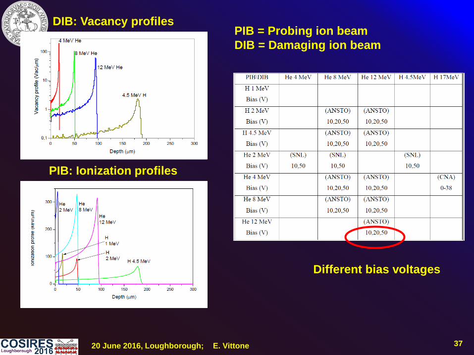
PIB = Probing ion beam
DIB = Damaging ion beam
DIB: Vacancy profiles
PIB: Ionization profiles
Different bias voltages
3820 June 2016, Loughborough; E. Vittone
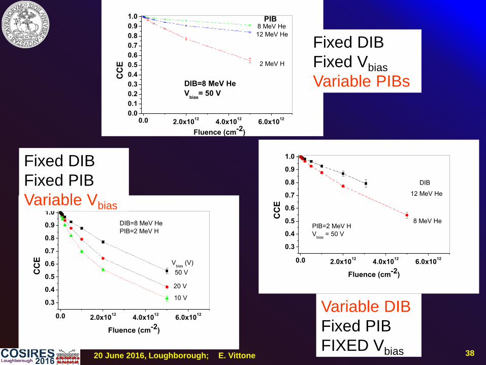
0.0 2.0x10¹²
4.0x10¹²
6.0x10¹²
0.0
0.1
0.2
0.3
0.4
0.5
0.6
0.7
0.8
0.9
1.0
DIB=8 MeV He
Vbias
= 50 V
8 MeV He
12 MeV He
CC
E
Fluence (cm-2
)
2 MeV H
PIB
Fixed DIB
Fixed Vbias
Variable PIBs
0.0 2.0x10¹²
4.0x10¹²
6.0x10¹²
0.3
0.4
0.5
0.6
0.7
0.8
0.9
1.0
10 V
20 V
50 V
Vbias
(V)
CC
E
Fluence (cm-2
)
DIB=8 MeV He
PIB=2 MeV H
0.0 2.0x10¹²
4.0x10¹²
6.0x10¹²
0.3
0.4
0.5
0.6
0.7
0.8
0.9
1.0
12 MeV He
8 MeV He
DIB
CC
EFluence (cm
-2)
PIB=2 MeV H
Vbias
= 50 V
Variable DIB
Fixed PIB
FIXED Vbias
Fixed DIB
Fixed PIB
Variable Vbias

3920 June 2016, Loughborough; E. Vittone
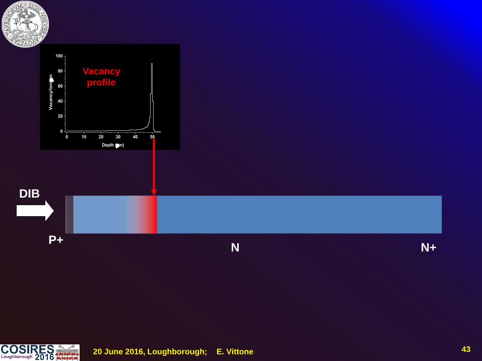
0 10 20 30 40 50
0
20
40
60
80
100
Vacan
cy/i
on
/m
Depth (m)
Vacancy
profile
P+N N+
DIB
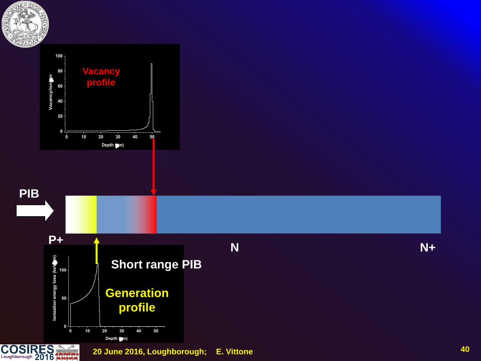
4020 June 2016, Loughborough; E. Vittone
0 10 20 30 40 50
0
20
40
60
80
100
Vacan
cy/i
on
/m
Depth (m)
Vacancy
profile
0 10 20 30 40 500
50
100
Ion
izati
on
en
erg
y l
oss (
keV
m)
Depth (m)
P+N N+
PIB
Generation
profile
Short range PIB
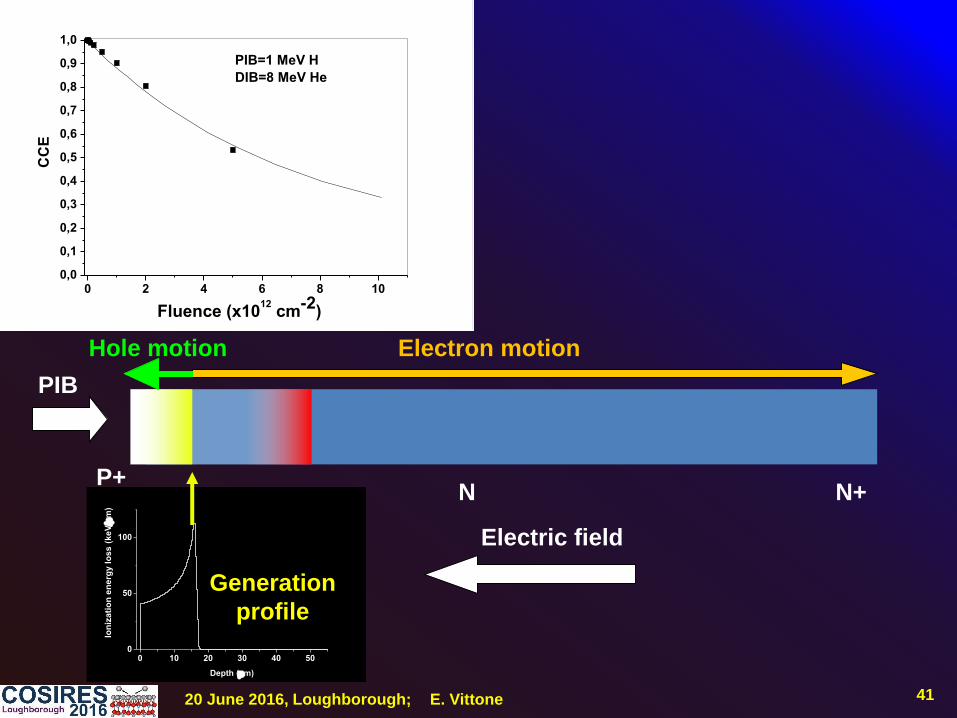
4120 June 2016, Loughborough; E. Vittone
0 10 20 30 40 500
50
100
Ion
izati
on
en
erg
y l
oss (
keV
m)
Depth (m)
P+N N+
PIB
Electric field
Electron motionHole motion
Generation
profile
0 2 4 6 8 100,0
0,1
0,2
0,3
0,4
0,5
0,6
0,7
0,8
0,9
1,0C
CE
Fluence (x1012
cm-2
)
PIB=1 MeV H
DIB=8 MeV He
4220 June 2016, Loughborough; E. Vittone
0 2 4 6 8 100,0
0,1
0,2
0,3
0,4
0,5
0,6
0,7
0,8
0,9
1,0C
CE
Fluence (x1012
cm-2
)
PIB=1 MeV H
DIB=8 MeV He
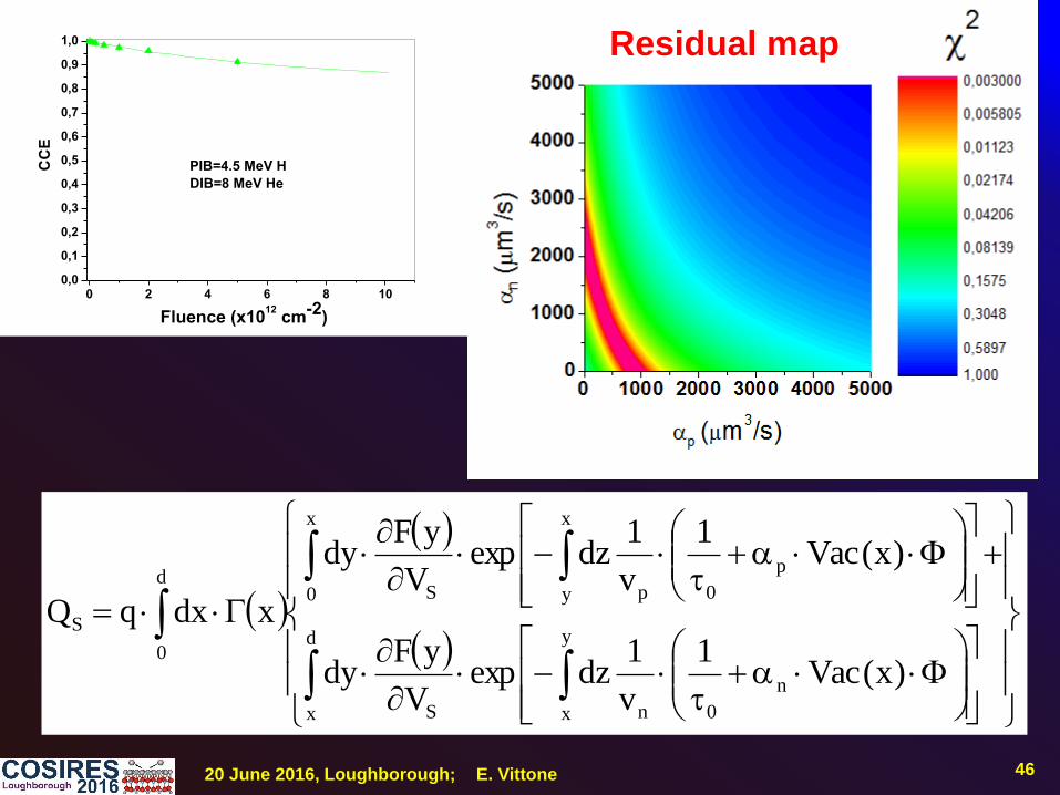
Residual map
d
0
d
x
y
x
n
0nS
S )x(Vac1
v
1dzexp
V
yFdyxdxqQ
n Free parameter
4320 June 2016, Loughborough; E. Vittone
0 10 20 30 40 50
0
20
40
60
80
100
Vacan
cy/i
on
/m
Depth (m)
Vacancy
profile
P+N N+
DIB
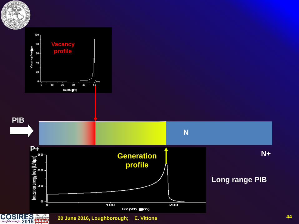
4420 June 2016, Loughborough; E. Vittone
0 100 200
0
30
60
90
Ioni
zatio
n en
ergy
loss
(keV
m
)
Depth (m)
0 10 20 30 40 50
0
20
40
60
80
100
Vacan
cy/i
on
/m
Depth (m)
Vacancy
profile
P+
N
N+
PIB
Generation
profile
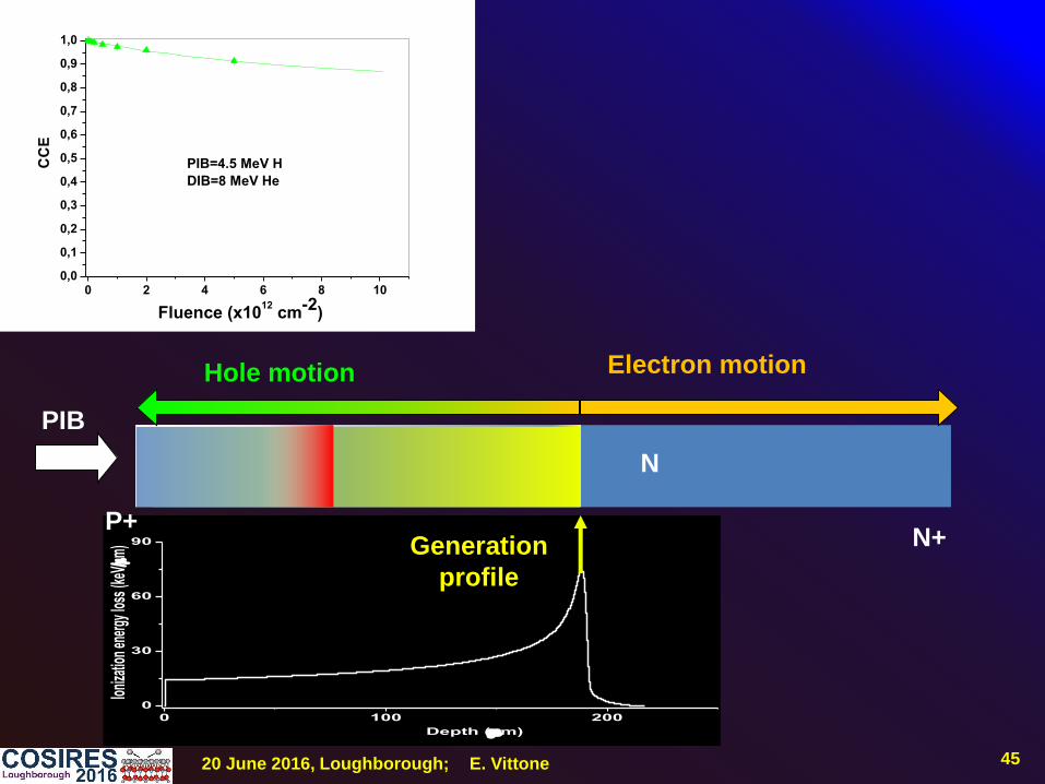
Long range PIB
4520 June 2016, Loughborough; E. Vittone
0 100 200
0
30
60
90
Ioni
zatio
n en
ergy
loss
(keV
m
)
Depth (m)
0 10 20 30 40 50
0
20
40
60
80
100
Vacan
cy/i
on
/m
Depth (m)
Vacancy
profile
P+
N
N+
PIB
Generation
profile
Electron motionHole motion
0 2 4 6 8 100,0
0,1
0,2
0,3
0,4
0,5
0,6
0,7
0,8
0,9
1,0C
CE
Fluence (x1012
cm-2
)
PIB=4.5 MeV H
DIB=8 MeV He
4620 June 2016, Loughborough; E. Vittone
0 10 20 30 40 50
0
20
40
60
80
100
Vacan
cy/i
on
/m
Depth (m)
Vacancy
profile
0 2 4 6 8 100,0
0,1
0,2
0,3
0,4
0,5
0,6
0,7
0,8
0,9
1,0C
CE
Fluence (x1012
cm-2
)
PIB=4.5 MeV H
DIB=8 MeV He
Residual map
d
0d
x
y
x
n
0nS
x
0
x
y
p
0pS
S
)x(Vac1
v
1dzexp
V
yFdy
)x(Vac1
v
1dzexp
V
yFdy
xdxqQ
4720 June 2016, Loughborough; E. Vittone
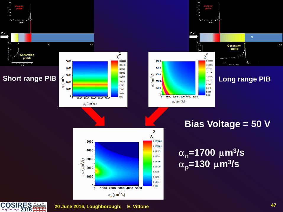
Short range PIB Long range PIB
n=1700 m3/s
p=130 m3/s
Bias Voltage = 50 V

4820 June 2016, Loughborough; E. Vittone
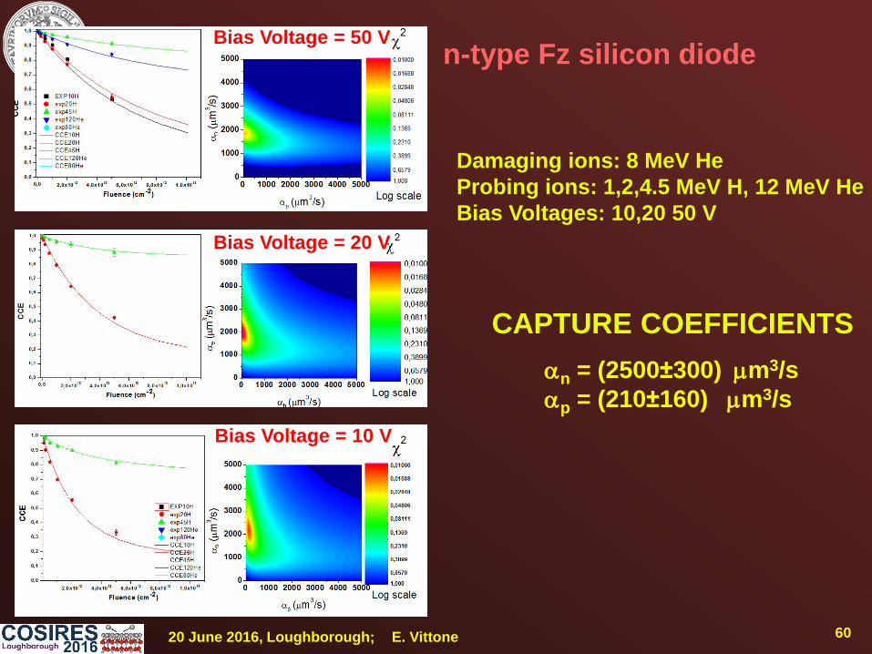
Damaging ions: 8 MeV He
Probing ions: 1,2,4.5 MeV H, 12 MeV He
Bias Voltages: 10,20 50 V
n-type Fz silicon diode
N-typeP-type
4920 June 2016, Loughborough; E. Vittone
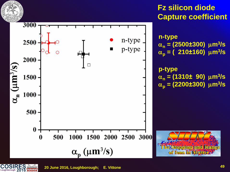
Fz silicon diode
Capture coefficient
n-type
n = (2500±300) m3/s
p = ( 210±160) m3/s
p-type
n = (1310± 90) m3/s
p = (2200±300) m3/s

5020 June 2016, Loughborough; E. Vittone
N-type silicon
DLTS measurements
singly V2(−/0) negatively charged divacancy
σn≈5·10-15 cm2
0 5 10 15 20 25 30 35 40 45 50 55 6010
-3
10-2
10-1
100
101
102
8 MeV He
Va
ca
nc
y/Io
n/
m
Depth (m)
Vacancy Marlowe
di-Vacancy Marlowe
Vacancy SRIM
From MARLOWE
simulation
n=vthσn
σn≈(3.6±0.4)·10-15 cm2
C. R. Crowell,
Appl. Phys. 9, 79-81, 1976
Vth= 1.8 ·107 m/s
5120 June 2016, Loughborough; E. Vittone
d
0d
x
y
x
n
0nS
x
0
x
y
p
0pS
S
)x(Vac1
v
1dzexp
V
yFdy
)x(Vac1
v
1dzexp
V
yFdy
xdxqQ
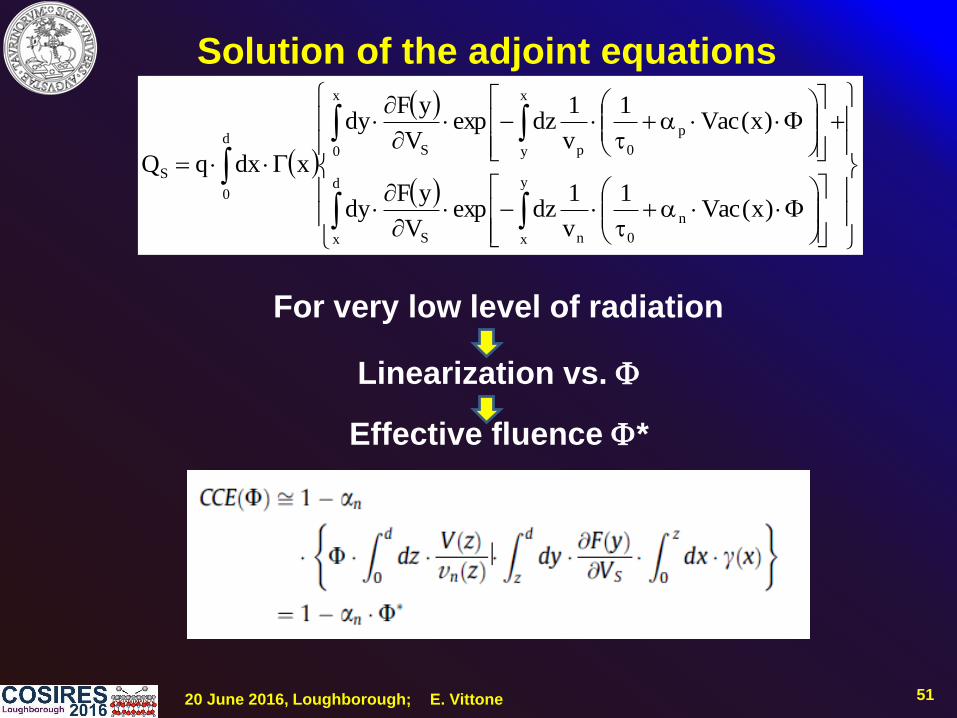
Solution of the adjoint equations
For very low level of radiation
Linearization vs.
Effective fluence *
5220 June 2016, Loughborough; E. Vittone
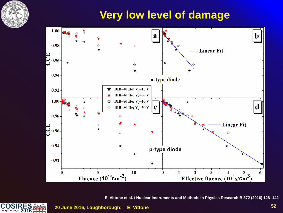
Very low level of damage
E. Vittone et al. / Nuclear Instruments and Methods in Physics Research B 372 (2016) 128–142
5320 June 2016, Loughborough; E. Vittone
Derivation of the Non Ionizing Energy Loss
(NIEL) displacement damage formula
Constant vacancy profile
Low displacement damage
ded DK1CCE
z
0
d
z
z
0 S
eff
pp
d
z S
eff
nn
R
0
ed xdxV
yFdy)z(kxdx
V
yFdy)z(kdz
MK
Ked = equivalent damage factor depends on
Electrostatics of the device
Carrier transport and recombination
Ion probe ionization profile
5420 June 2016, Loughborough; E. Vittone
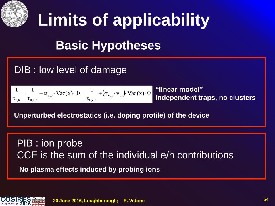
Limits of applicability
)x(Vacv1
)x(Vac11
thh,e
h,e,0
p,n
h,e,0h,e
Basic Hypotheses
DIB : low level of damage
“linear model”
Independent traps, no clusters
Unperturbed electrostatics (i.e. doping profile) of the device
PIB : ion probe
CCE is the sum of the individual e/h contributions
No plasma effects induced by probing ions

5520 June 2016, Loughborough; E. Vittone
An experimental protocol has been proposed to study the radiation hardness
of semiconductor devices
Under the assumption of low damage level,
the CCE degradation of a semiconductor device induced by ions of different
mass and energy can be interpreted by means of a model based on
•The Shockley-Ramo-Gunn theorem for the charge pulse formation
•The Shockley-Read-Hall model for the trapping phenomena
If the generation occurs in the depletion region, an analytical solution of the
adjoint equation can be calculated.
Adjusted NIEL scaling can be derived from the general theory in the case of
constant vacancy profile.
The model leads to the evaluation of the capture coefficient.
CONCLUSIONS
The capture coefficient is directly related to the
radiation hardness of the material

5620 June 2016, Loughborough; E. Vittone
COOPERATION AND MUTUAL
UNDERSTANDING LEAD TO GROWTH
AND GLOBAL ENRICHMENT
IAEA Coordinate Research Programme (CRP) F11016 (2011-2015)
“Utilization of ion accelerators for studying and modeling of radiation
induced defects in semiconductors and insulators”
NUS
Ruđer Bošković Inst.
Delhi Univ.
ANSTOHelsinki Univ.
CAN
JAEA-Kyoto Univ.
Malesian Nuclear Agency
Torino Univ.
Surrey Univ.
SANDIA
Leipzig Univ.
5720 June 2016, Loughborough; E. Vittone
Characterization of radiation induced damage:
ded
0
DK1K1Y
Y
Device characteristics
before irradiation
Equivalent
damage factor
Particle
Fluence
Displacement
dose
Device characteristic after irradiation
First order: proportionality, independent of the particle, between the damage factor
and the particle NIEL
NIEL approach:
measurement of Ked only for one
particle (at one specific energy)
Ked can be estimated for all
the particles and energies

5820 June 2016, Loughborough; E. Vittone
ded
0
DK1K1Q
QCCE
Induced Charge
before irradiation
Induced Charge after irradiation
Characterization of radiation induced damage:
Equivalent
damage factor
Particle
Fluence
Displacement
dose

5920 June 2016, Loughborough; E. Vittone
n
n*
n0n
nGnDn
t
n
Excess carrier lifetime
thtrap vN
1
Trap density Thermal velocity
Capture cross section
K
11
0
kNN traptrap
0 Trap density induced by
radiation
Trap density in pristine
material
6020 June 2016, Loughborough; E. Vittone
Damaging ions: 8 MeV He
Probing ions: 1,2,4.5 MeV H, 12 MeV He
Bias Voltages: 10,20 50 V
n-type Fz silicon diodeBias Voltage = 50 V
Bias Voltage = 20 V
Bias Voltage = 10 V
n = (2500±300) m3/s
p = (210±160) m3/s
CAPTURE COEFFICIENTS