modeling of high voltage devices for esd event simulation ...€¦ · the bjt does not turn-on...
TRANSCRIPT

The World Leader in High Performance Signal Processing Solutions
WCM 2011, June 15-16, Boston
Modeling of High Voltage Devices for
ESD Event Simulation in SPICE
Yuanzhong (Paul) Zhou,
Javier A. Salcedo
Jean-Jacques Hajjar
Analog Devices Inc.
Wilmington, MA, USA

Y. Zhou, J. Salcedo, J.J. Hajjar 2
INTRODUCTION
ESD & general ESD protection scheme
Background of SPICE ESD simulation for HV devices
HV LDMOS DEVICES AND ESD PROTECTION
High voltage NLDMOS devices
HV ESD protection clamp
SNAPBACK MODELING
Operation of LDMOS and HV clamp
Snapback models for LDMOS and HV clamp
MEASUREMENT AND SIMULATION
CONCLUSION
Outline
WCM 2011, June 15-16, Boston

Y. Zhou, J. Salcedo, J.J. Hajjar 3
ESD: Electrostatic Discharge
Sudden electrostatic charge transfer between two objects at different potentials
Causes:
Tribo-electric charging and electrical field induction
In ICs:
Occurs in human handling and testing
Characteristics: Large currents and high voltages Short in duration (1~150 ns)
Introduction
-- What is ESD?
WCM 2011, June 15-16, Boston
from RTP Company, Winona, MN

Y. Zhou, J. Salcedo, J.J. Hajjar 4
ESD causes damages in ICs
Catastrophic failures: contact spiking, junction burnout, gate oxide rupture, metal burnout
Latent failures: degradation of gate oxide, partial opens in metals
Costly failure mechanism
Costs electronics industry >$84B in lost profits per year (4~8% of total annual revenue! )*
Responsible to >30% customer returns
(* M. Brandt & S. Halperin, Circuits Assembly Magazine, June 1, 2003)
WCM 2011, June 15-16, Boston
Why focus on ESD?
DRAIN-CHANNEL
JUNCTION DAMAGEDRAIN CONTACT
SPIKING
DRAIN CHANNEL SOURCE
Root-cause of customer returnsMerrill et al., Proc. ESD/EOS Symposium, 1993

Y. Zhou, J. Salcedo, J.J. Hajjar 5
On-Chip ESD Protection Scheme
WCM 2011, June 15-16, Boston
IN OUT
VDD
VSS
CORE CIRCUIT
ES
D
ES
D
ES
D
ES
DE
SD
Objective: protect IC from ESD damages1. Shunt current discharges away from the CORE CIRCUIT
2. Clamps I/O & Power pad voltage to a safe level
Interaction of ESD protection and core circuitry
Ideally, ESD structures are transparent to internal circuitry
In reality, the protection and core circuitries impact each other’s performance
IN OUT
VDD
VSS
CORE CIRCUIT
ESD
ESD
ESD
ESD
ESD

Y. Zhou, J. Salcedo, J.J. Hajjar 6
BCDMOS technology is key in mixed-signal
applications for multiple sectors
Co-design is required for robust ESD protection
design and circuit optimization in high voltage
mixed-signal applications
Circuit-level simulation provides useful insight in
the interaction between ESD protection and core
circuitry
Simulation can reduce design iteration and cost
that typically occur in trial-and-error approaches
WCM 2011, June 15-16, Boston
Motivation of SPICE ESD simulation
for HV Devices

Y. Zhou, J. Salcedo, J.J. Hajjar
SPICE ESD Simulation for HV Devices
Co-Design Conditions
7WCM 2011, June 15-16, Boston
n-p-n
VL
VH’
VGControl Circuit HV
Clamp
VHRIOControl Circuit
I/O_1 I/O_2
Body
n-p-nRB
HV Device Between
Two I/O Pads
HV Device HV
Protection Clamp
Co-design

Y. Zhou, J. Salcedo, J.J. Hajjar 8
A key requirement for ESD simulation is the availability
of compact models accurate for ESD operation
ESD modeling for HV devices is very challenging Devices operate in extreme bias conditions
Structure complexity of LDMOS and HV clamps
There are very few reported modeling efforts which are
either not self-consistent or have limited availability
SPICE simulation using macromodel approach has been
demonstrated successful in low voltage technologies
Similar modeling approach for HV LDMOS devices and
HV clamps will be presented in this paper
WCM 2011, June 15-16, Boston
Background of SPICE Modeling for
HV ESD Devices

Y. Zhou, J. Salcedo, J.J. Hajjar 9
Non-uniform channel doping
Lightly doped N-Well/Deep N-Well drift region
LDMOS DEVICES AND ESD PROTECTION
-- High Voltage NLDMOS devices
WCM 2011, June 15-16, Boston
S BG S
P+ N+
P-Well
P-Substrate
D G
N+
N-Well
D G
N+
N-Well
N+
P-Field
Deep N-Well
Y. Zhou, J. Salcedo, J.J. Hajjar 10
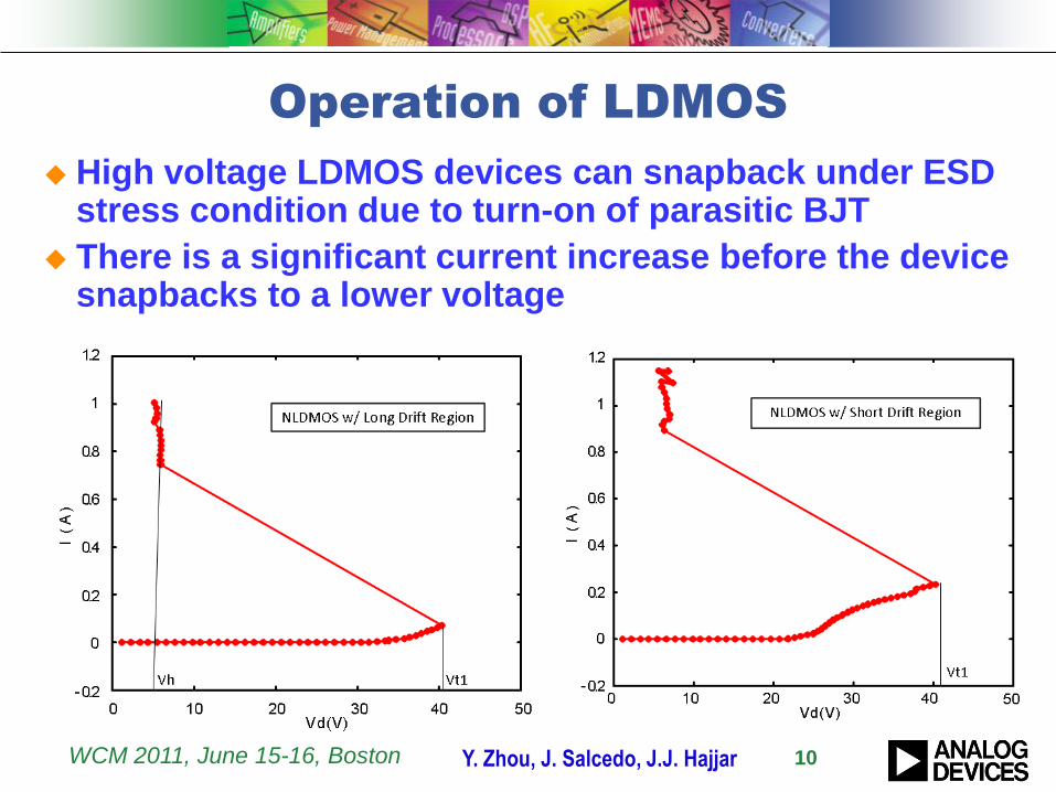
Operation of LDMOS
High voltage LDMOS devices can snapback under ESD stress condition due to turn-on of parasitic BJT
There is a significant current increase before the device snapbacks to a lower voltage
WCM 2011, June 15-16, Boston
Y. Zhou, J. Salcedo, J.J. Hajjar 11
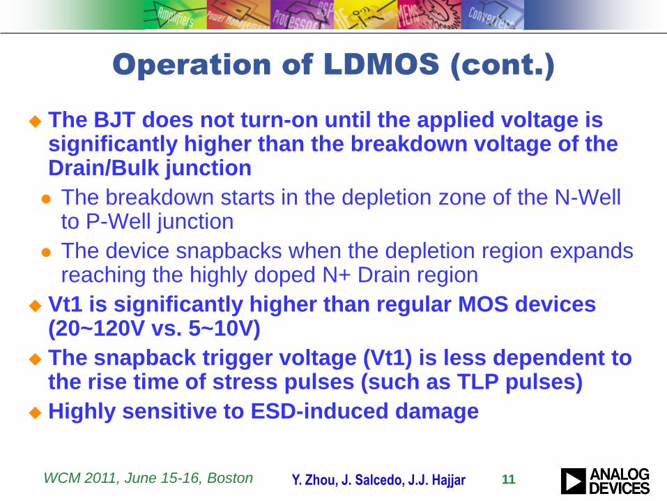
Operation of LDMOS (cont.)
The BJT does not turn-on until the applied voltage is significantly higher than the breakdown voltage of the Drain/Bulk junction
The breakdown starts in the depletion zone of the N-Well to P-Well junction
The device snapbacks when the depletion region expands reaching the highly doped N+ Drain region
Vt1 is significantly higher than regular MOS devices (20~120V vs. 5~10V)
The snapback trigger voltage (Vt1) is less dependent to the rise time of stress pulses (such as TLP pulses)
Highly sensitive to ESD-induced damage
WCM 2011, June 15-16, Boston

Y. Zhou, J. Salcedo, J.J. Hajjar 12
Key Components and Effects in
LDMOS Snapback
Key components: main LDMOS, parasitic BJT, back-gate resistance, P-well/N-well diode
Key effects: avalanche current at Drain/Back-gate (Collector/Base) junction, voltage drop across the back-gate resistance, P-well/N-well diode breakdown
WCM 2011, June 15-16, Boston
Y. Zhou, J. Salcedo, J.J. Hajjar 13
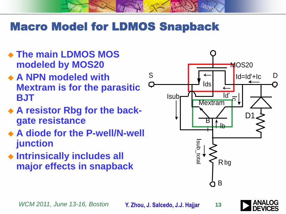
Macro Model for LDMOS Snapback
The main LDMOS MOS modeled by MOS20
A NPN modeled with Mextram is for the parasitic BJT
A resistor Rbg for the back-gate resistance
A diode for the P-well/N-well junction
Intrinsically includes all major effects in snapback
WCM 2011, June 13-16, Boston
MOS20
Mextram
IbB
i
Isu
b_
tota
l R bg
Id=Id'+Ic
Ic
Ids
Id'
S D
B
Isub
D1
Y. Zhou, J. Salcedo, J.J. Hajjar 14
LDMOS DEVICES AND ESD PROTECTION
-- ESD protection clamp
WCM 2011, June 13-16, Boston
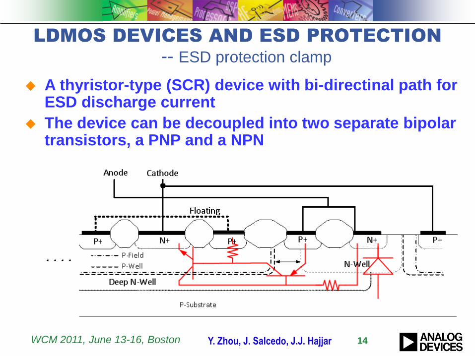
A thyristor-type (SCR) device with bi-directinal path for ESD discharge current
The device can be decoupled into two separate bipolar transistors, a PNP and a NPN

Y. Zhou, J. Salcedo, J.J. Hajjar 15
Operation of HV Clamp
The clamp works in snapback mode as a result of the positive feedback triggered by the avalanche current in the PNP and NPN
In snapback, one BJT activates first and then subsequently the second one turns on
The Vt1 is more determined by the first BJT while the second one has bigger impact on Vh
The weaker the second BJT is, the higher the Vh
Used as protection for LDMOS at I/O or as power clamp
High Vt1 and sometimes high Vh are required for HV clamping
WCM 2011, June 13-16, Boston

Y. Zhou, J. Salcedo, J.J. Hajjar 16
Macro Model for Thyristor-like Clamp
WCM 2011, June 15-16, Boston
Qnpn
Qpnp
Cathode
Anode
Rpw
Rnw
Substrate
Dnwsub
The model includes the NPN, PNP, avalanche effect, and resistive voltage drop Vbe in the both BJT’s
The clamp is modeled by incorporating an advanced BJT (NPN) model with two resistors
Rpw =1MΩ for floating Pwell
The NPN model includes both the avalanche and junction capacitance and has a parasitic PNP that is used for the Qpnp

Y. Zhou, J. Salcedo, J.J. Hajjar 17
Transmission Line Pulse (TLP)
Measurement Setup Introduction
+
-
High voltage
supply
Transmission Line; Z0 = 50
DUT
Termination
ZT1
ZT2
+
-
High voltage
supply
Transmission Line; Z0 = 50
DUT
Termination
ZT1
ZT2
.......
time
I
Experimental data were measured with TLP technique
Apply a sequence of rectangular pulses to two terminals of a DUT
Use stabilized I-V curves as measurement results
VTLP
ITLP
VTLP
ITLP
IDUT (t)
t rise VTLP
ITLP
IDUT (t)
t rise VTLP
ITLP
VDUT (t)VDUT (t)
Current Probe
ZATTZATT
Current Probe
(Vt2, It2)
Vt1
WCM 2011, June 15-16, Boston

Y. Zhou, J. Salcedo, J.J. Hajjar 18
Simulation Setup for Snapback Effect
Snapback effect was simulated with transient simulation
Voltage Pulse Sequence (100ns) were used as the Input
The stabilized VD and ID were measured as the simulation results (~80ns).
WCM 2011, June 15-16, Boston
Schematic of
Snapback Simulation

Y. Zhou, J. Salcedo, J.J. Hajjar 19
Simulation Results vs. TLP Measurement
-- NLDMOS device (W=5000um , trise=10ns)
WCM 2011, June 15-16, Boston
Y. Zhou, J. Salcedo, J.J. Hajjar 20
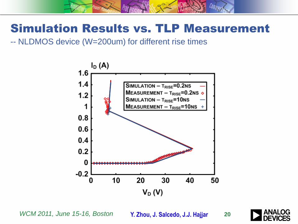
Simulation Results vs. TLP Measurement
-- NLDMOS device (W=200um) for different rise times
WCM 2011, June 15-16, Boston

Y. Zhou, J. Salcedo, J.J. Hajjar 21
Simulation Results vs. TLP Measurement
-- NLDMOS device (W=200um) with longer drift region
WCM 2011, June 15-16, Boston

Y. Zhou, J. Salcedo, J.J. Hajjar 22
Simulation Results vs. TLP Measurement
-- a low holding voltage clamp in the 0.35um process (trise=10ns)
WCM 2011, June 15-16, Boston

Y. Zhou, J. Salcedo, J.J. Hajjar 23
Simulation Results vs. TLP Measurement
-- a high holding voltage clamp in the 0.18um process
WCM 2011, June 15-16, Boston

Y. Zhou, J. Salcedo, J.J. Hajjar 24
Modeling ESD behavior of high voltage LDMOS and thyristor-like clamp devices using a macro model approach has been presented.
The models consisted of standard passive and active components without having to use a complex external dependent current source.
The simplicity of this modeling approach facilitates easy implementation of the methodology.
The simulation results have shown good agreement with measured TLP data as performed on 0.18-um and 0.35-um BCDMOS process technologies.
Conclusion
WCM 2011, June 15-16, Boston

Y. Zhou, J. Salcedo, J.J. Hajjar 25
Acknowledgement
Slavica Malobabic: For contributions on devices’
characterization, TCAD simulation and insightful discussion
on the results presented in this paper.
Srivatsan Parthasarathy: For valuable inputs on the
development of this work.
WCM 2011, June 15-16, Boston