modelling leakage
TRANSCRIPT
MODELING LEAKAGE IN SUB-MICRON CMOS TECHNOLOGIES
Behnaz Mortazavi B.Sc. E.E., Azad University of Tehran-Iran, 1995
PROJECT SUBMITTED IN PARTIAL FULFILLMENT OF THE REQUIREMENTS FOR THE DEGREE OF
MASTER OF ENGINEERING
In the School of
Engineering Science
O Behnaz Mortazavi 2004
SIMON FRASER UNIVERSITY
Fall 2004
All rights reserved. This work may not be reproduced in whole or in part, by photocopy
or other means, without permission of the author.
APPROVAL
Name:
Degree:
Title of Project:
Behnaz Mortazavi
Master of Engineering
Modeling Leakage in Sub-Micron CMOS Technologies
Supervisory Committee:
Chair: Dr. Bozena Kaminska
Dr. Marek Syrzycki
Senior Supervisor Professor of School of Engineering
Dr. Ash Parameswaran Supervisor Professor of School of Engineering
Date DefendedIApproved: Dec 3rd, 2004
SIMON FRASER UNIVERSITY
PARTIAL COPYRIGHT LICENCE
The author, whose copyright is declared on the title page of this work, has granted to Simon Fraser University the right to lend this thesis, project or extended essay to users of the Simon Fraser University Library, and to make partial or single copies only for such users or in response to a request from the library of any other university, or other educational institution, on its own behalf or for one of its users.
The author has further granted permission to Simon Fraser University to keep or make a digital copy for use in its circulating collection.
The author has further agreed that permission for multiple copying of this work for scholarly purposes may be granted by either the author or the Dean of Graduate Studies.
It is understood that copying or publication of this work for financial gain shall not be allowed without the author's written permission.\
Permission for public performance, or limited permission for private scholarly use, of any multimedia materials forming part of this work, may have been granted by the author. This information may be found on the separately catalogued multimedia material and in the signed Partial Copyright License.
The original Partial Copyright License attesting to these terms, and signed by this author, may be found in the original bound copy of this work, retained in the Simon Fraser University Archive.
W. A. C. Bennett Library Simon Fraser University
Bumaby, BC, Canada

ABSTRACT
As CMOS technology scaling continues, subthreshold leakage current increases
dramatically. A significant percentage of the total chip power is due to leakage, also
known as static power. Accurately estimating static power in early stages of design is an
important step for developing power efficient products.
Leakage current is an important segment of total supply current (IDDQ), which is
used as a means to identify defective chips. ID^^ value is determined by the sum of
leakage currents of those transistors that can leak. Setting ID^^ value too high or low will
result in excessive shipment of defective chips or yield loss because of rejecting good
parts, respectively.
The goal of this work is to investigate and model leakage mechanisms in
submicron CMOS technology using SPICE circuit simulators. The main focus of this
research will be subthreshold and reverse-bias p-n junction band-to-band leakage
mechanisms and the effect of transistor parameters on them.

DEDICATION
To my love and husband, Ali, for his unconditional and
never-ending love, support, and patience
ACKNOWLEDGEMENTS
I would like to thank Dr. Marek Syrzycki, my senior supervisor, for sharing his
knowledge with me and for his help and guidance throughout the course of this project.
His prompt response to my problems made it possible to keep to the demanding schedule.
I would also like to thank Dr. Ash Parameswaran for accepting to be my
supervisor and committee member and for his constructive feedback on this work.
Thanks to my parents for their continuous support and encouragement for
acquiring higher levels of education.
Finally, I would like to thank all those who have directly or indirectly helped me
in this work.
TABLE OF CONTENTS
.. Approval ............................................................................................................................ 11
... Abstract ............................................................................................................................. 111
Dedication ......................................................................................................................... iv
Acknowledgements ............................................................................................................ v
Table of Contents ............................................................................................................. vi ...
List of Figures ................................................................................................................. vlu
...................................................................................................................... List of Tables x
................................................................................................................ 1 Introduction 1
2 Leakage Mechanisms ................................................................................................. 4 ........................................................................................... 2.1 Subthreshold Leakage 6
2.1.1 Weak Inversion Effect .................................................................................... 6 ....................................................... 2.1.2 Drain Induced Barrier Lowering (DIBL) 6
2.1.3 Body Effect .................................................................................................... 6 2.1.4 Narrow Width Effect ...................................................................................... 7 2.1.5 Effect of Channel Length ............................................................................... 7
................................................................................................... 2.1.6 Temperature 8 ........................................................................ 2.2 Reverse-bias pn Junction Leakage 8
.................................................................... 2.3 Gate-induced Drain Leakage (GIDL) 8 2.4 Channel Punch-through Leakage .......................................................................... 9
.................................................................................... 2.5 Oxide Tunnelling Leakage 9 .................................................................... 2.6 Hot Carrier Injection Gate Leakage 10
........................................................................ 3 Parameter Dependence of Leakage 11
............................................................. 4 SPICE Simulation of Submicron Leakage 13 .................................................................................................. 4.1 B SIM3 MODEL 15
..................................................................................... 4.2 0.35.micron Technology 16 4.2.1 I-V Characteristics ........................................................................................ 16
.......................................................................................... 4.2.1.1 A Case Study 20 ....................................................... 4.2.1.2 Drain-Bulk Junction Current (Ij. DB ) 28
........................................................................... 4.2.2 Channel Length Variations 30 ......................................................................... 4.2.3 Oxide Thickness Variations 30 .......................................................................... 4.2.4 Channel Doping Variations 30
...................................................................... 4.2.5 Threshold Voltage Variations 32 . . .............................................................................................. 4.2.6 VDD Var~atlons 32 ...................................................................................................... 4.2.7 Summary 34
vii
4.3 0.1 8-micron Technology ..................................................................................... 35 4.3.1 I-V Characteristics ........................................................................................ 35 4.3.2 Channel Length Variations ........................................................................... 38 4.3.3 Oxide Thickness Variations ......................................................................... 39
.......................................................................... 4.3.4 Channel Doping Variations 39 ...................................................................... 4.3.5 Threshold Voltage Variations 39 . .
4.3.6 VDD Var~atlons .............................................................................................. 39 ...................................................................................................... 4.3.7 Summary 42
4.4 0.13-micron Technology ..................................................................................... 43 4.4.1 I-V Characteristics ........................................................................................ 43 . . 4.4.2 Channel Length Var~atlons ........................................................................... 46 4.4.3 Oxide Thickness Variations ......................................................................... 47 4.4.4 Channel Doping Variations .......................................................................... 47 4.4.5 Threshold Voltage Variations ...................................................................... 47 . . .............................................................................................. 4.4.6 VDD Variations 47 4.4.7 Summary ...................................................................................................... 50
5 Conclusion ................................................................................................................. 51
6 References ................................................................................................................. 53
... Vl l l
LIST OF FIGURES
Figure 1:
Figure 2: Figure 3: Figure 4: Figure 5: Figure 6:
Figure 7: Figure 8:
Figure 9: Figure 10:
Figure 1 1 : Figure 12: Figure 13: Figure 14:
Figure 1 5 : Figure 1 6:
Figure 17: Figure 18: Figure 19: Figure 20: Figure 2 1 : Figure 22:
Figure 23: Figure 24: Figure 25: Figure 26:
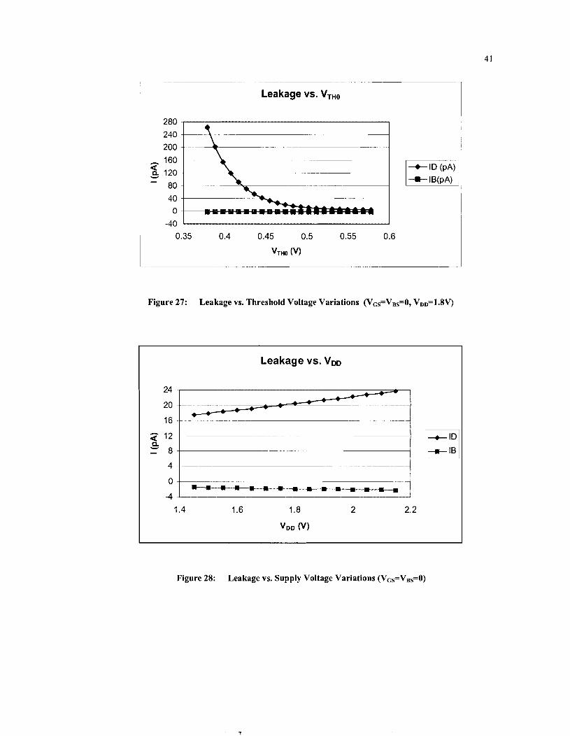
Figure 27: Figure 28:
Threshold Voltage Scaling and Increase in OFF Current for a Given Technology [2] ............................................................................................... 1 Technology Scaling and Leakage Power Increase [2] ................................... 2 Leakage Mechanisms in Sub-micron CMOS Transistor [5] .......................... 5 Circuit Schematic for Leakage Simulation .................................................. 13 DC Circuit Equivalent of MOS Transistor in BSIM3 Model [lo] ............... 15 ID-V Characteristics of NMOS (W/L=0.8/0.35. VDDX3.3V) ........................ 17
IB-V Characteristics of NMOS (W/L=0.8/0.35. VDD=3 . 3V) ........................ 18 Measurement of Bulk Current vs . VGS at Various VBs. VDD=l . 5V [12] ............................................................................................................... 20 Simulation of Bulk Current vs . VGS at Various VBs. VDD=1.5V .................. 21 Measurement - Drain Current vs . VGS at Various VBS. VDDZ1 . 5V [12] ............................................................................................................... 22 Simulation . Drain Current vs . VGS at Various VBS. VDD=I . 5V ................... 23 Drain Current Comparison for Ves=O. VDD=I . 5V ....................................... 24 Bulk Current Comparison for VBs=O. VDD=l . 5V ........................................ 25
.................................... Measurement - log lIBl vs . VGS at Various VDD [12] 26 Simulation - log IIBJ vs . VGS at Various VDD ................................................ 27 Comparison of Simulated and Measured Bulk Current (VDD=2 & 2.5V) ............................................................................................................. 28 Leakage vs . Channel Length Variations (VGs=V~s=O. V D D = ~ . ~ V ) ............. 31 Leakage vs . Oxide Thickness Variations (VGs=V~s=O. V D D = ~ . 3V) ............ 31 Leakage vs . Channel Doping Variations (VGs=V~s=O. V D D = ~ . ~ V ) ........... 32 Leakage vs . Threshold Voltage Variations (VGs=V~s=O. V D D = ~ . ~ V ) ........ 33
Leakage vs . Supply Voltage Variations (VGs=Vss=O) ................................ 33 ID-V Characteristics of NMOS (W/L=0.5/0.18. V D D = ~ . 8V) ........................ 36
. ........................ Ie-V Characteristics of NMOS (W/L=0.5/0.18. VDD=l 8V) 37 Leakage vs . Channel Length Variations (VGs=Vss=O. VDD=l . 8V) ............. 38 Leakage vs . Oxide Thickness Variations (VGs=Vss=O, VDD=l . SV) ............ 40 Leakage vs . Channel Doping Variations (VGS=VBS=O. VDD=l . 8V) ............ 40
Leakage vs . Threshold Voltage Variations (VGS=VBS=O. VDD=l . 8V) ........ 41 Leakage vs . Supply Voltage Variations (VGS=VB~=O) ............................. 41
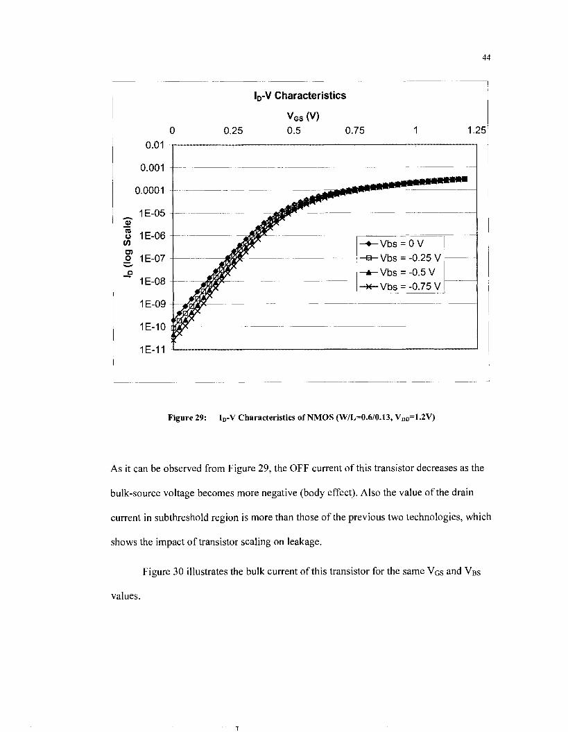
Figure 29: ID-V Characteristics of NMOS (W/L=0.6/0.13. V D D = ~ . 2V) ........................ 44
Figure 30: IB-V Characteristics of NMOS (W/L=0.6/0.13, VDD=l . 2V) ........................ 45 Figure 3 1 : Leakage vs . Channel Length Variations (VGs=VBs=O. VDDZ1 . 2V) ............. 46
Figure 32: Leakage vs . Oxide Thickness Variations (VG~=VBS=O. V D D = ~ . 2V) ............ 48 Figure 33 : Leakage vs . Channel Doping Variations (VGs=VBs=O. VDD=l . 2V) ........... 48 Figure 34: Leakage vs . Threshold Voltage Variations (VGs=VBs=O. V D D = ~ . 2V) ......... 49 Figure 35: Leakage vs . Supply Voltage Variations (VG~=VB~=O) ................................. 49
LIST OF TABLES
Table 1 : Parameter Dependence of Leakage Currents ............................................... 11 ............................................... Table 2: Gate Oxide Thickness in Submicron CMOS 14
Table 3: Parameter Variation Summary for 0.35 micron Technology ....................... 34 ....................... Table 4: Parameter Variation Summary for 0.18 micron Technology 42
Table 5: Parameter Variation Summary for 0.13 micron Technology ....................... 50 Table 6: Dominant Leakage Parameter in CMOS Technologies ............................... 51
1 INTRODUCTION
The need for lower power consumption and higher circuit densities has made it
necessary to scale down supply voltage in CMOS logic circuits. To maintain the circuit
speed, threshold voltage should also scale down with the supply voltage. This results in
leakage current increase (See Figure 1); and hence, the leakage power increases with each
technology node. If this trend continues, leakage power will soon be in the same order as
the dynamic power (See Figure 2). Estimating leakage power in early stages of VLSI
circuit design is important for optimizing the total power dissipation [I] .
Figure 1: Threshold Voltage Scaling and Increase in OFF Current for a Given Technology 121
1.0 .8 .6 .35 .25 . I 8 . I 3
Technology (micron)
Figure 2: Technology Scaling and Leakage Power Increase [2]
Leakage current is also an important factor in setting total supply current (IDDQ)
value, which is used as a passlfail threshold for testing chips. Setting this value too high
would cause some defective chips to be considered non-defective; similarly if this value
is set too low, functional chips may be considered defective. ID^^ consists of two parts,
the current due to parametric failure and the current due to catastrophic failure. The
parametric failure results in increased power supply current flow. Increasing leakage
current due to the technology scaling has reached or even passed the value of current
associated with parametric failure; this makes it more difficult to identify defective chips
PI.
All these have made researchers investigate ways to control and reduce leakage
current in submicron CMOS technologies. Two major categories for reducing leakage are
design-time, and run-time techniques. In [4] each of these techniques are explained. For
Design-Time Technique, use of Dual-Threshold CMOS is described; where, transistors
with low threshold voltage (VTH) are used in critical paths and high VTH transistors for
3
non-critical paths. For Run-Time technique, methods such as the use of transistor stacks,
sleep transistors, forward and reverse body biasing, and dynamic V T ~ scaling are
depicted.
There are several leakage sources in a MOSFET. Based on the transistor feature
size some of these leakage currents have higher values and therefore greater impact on
circuit performance than others.
In this report a number of leakage mechanisms will be studied. The impact of
important model parameters on leakage currents will be considered. SPICE simulation
will be performed on a MOS transistor in 0.35, 0.18, and 0.1 3 micron technology
generations. Leakage current comparison between a simulated transistor and a measured
one will be conducted, where applicable, followed by the conclusion.
2 LEAKAGE MECHANISMS
There are several parameters influencing the off current of a MOS transistor.
Threshold voltage, channellsurface doping profile, gate oxide thickness, channel physical
dimensions, drainlsource junction depth, and VDD all have some effects on the OFF
current. There are several leakage mechanisms contributing to the OFF current of a MOS
transistor in short channel devices. The dominating leakage mechanism depends on
device size, channel dimensions, operating conditions, technology node, and other
transistor parameters.
As the transistor channel length shortens, power supply of transistors needs to be
decreased and hence the threshold voltage. Since the weak inversion state leakage is a
function of threshold voltage, the OFF current of transistor increases. Increasing drain
voltage results in widening drain-channel depletion region and therefore drain current
increases significantly. The increase of the OFF current is due to the current on the
channel surface, which is caused by drain-induced barrier lowering (DIBL) or deep
channel punch-through currents. The threshold voltage and OFF current are both
dependant on the width of the transistor. As the width of the transistor decreases, these
two parameters get modulated and this gives rise to narrow-width effect. These
undesirable effects are called short channel effects (SCE).
To keep SCE under control, the gate oxide thickness needs to be reduced with
channel length scaling, which will result in considerable amount of current flowing
through the gate oxide of the transistor because of the high electric field. This means that
5
the input impedance of MOS transistors can't be considered infinite anymore and the
circuit performance will be seriously degraded. The two major components of gate
leakage current are injection of hot carriers from substrate to the gate oxide and gate
oxide tunnelling.
Depletion of the carriers at the drain surface right below the gate-drain overlap
causes another leakage current called gate-induced drain leakage (GIDL). All of the
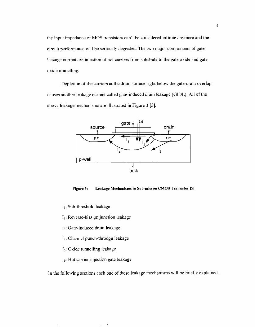
above leakage mechanisms are illustrated in Figure 3 [ 5 ] .
gate 7 '5,6 SOU rce I drain
? I ? n +
b bulk
Figure 3: Leakage Mechanisms in Sub-micron CMOS Transistor [S]
1, : Sub-threshold leakage
12: Reverse-bias pn junction leakage
13: Gate-induced drain leakage
14: Channel punch-through leakage
Is: Oxide tunnelling leakage
I ~ : Hot carrier injection gate leakage
In the following sections each one of these leakage mechanisms will be briefly explained.
2.1 Subthreshold Leakage
Subthreshold leakage in a MOS transistor is caused by several phenomena,
which are described in the following sections.
2.1.1 Weak Inversion Effect
Weak inversion happens when the gate voltage is below threshold voltage. In this
mode the minority carrier concentration in the conduction channel is low but not zero.
The drain-substrate voltage drops entirely across the substrate-drain pn junction, which is
reverse biased. Since both the longitudinal electric field and the number of mobile carries
are small, the diffusion current dominates. This is one of the components of the
subthreshold current [ 5 ] .
2.1.2 Drain Induced Barrier Lowering (DIBL)
DIBL happens when source and drain depletion regions interact with each other
close to the channel surface. High drain voltage in a short channel device lowers the
source barrier height and hence decreases the threshold voltage. As a consequence the
source injects carriers into the channel surface. Gate voltage does not have any effect on
this phenomenon. As the channel length decreases and the drain voltage increases, DIBL
effect becomes more and more significant [ 5 ] .
2.1.3 Body Effect
When the well-source junction in a MOS transistor is reverse biased, the bulk
depletion region widens and this increases the threshold voltage. The increase in
threshold voltage causes the leakage current to decrease [ 5 ] .
2.1.4 Narrow Width Effect
Narrow width of a MOS transistor modulates the threshold voltage and the
leakage current in 3 different ways.
The fringing field of the gate causes the gate-induced depletion region to extend
outside the channel width and consequently to increase the total depletion charge of the
bulk region. This increases the threshold voltage.
The channel doping is higher along the width of the local oxide isolation gate.
Because of the channel stop, the dopants invade under the gate. This means that there is
need for higher voltage to invert the channel.
The third effect is called inverse-narrow-width effect. In this case the depletion
layer cannot extend under the oxide isolation; so the depletion charge in the bulk doesn't
rise. But, because of the field induced edge-fringing effect at the gate edge, an inversion
layer at the gate edges forms at lower voltage than at the centre. And the overall gate
capacitance increases because of the sidewall capacitance; and therefore, the threshold
voltage decreases [ 5 ] .
2.1.5 Effect of Channel Length
In short channel transistors, the drain and source depletion regions are in a near
proximity of each other. They enter more into the channel length and as a result part of
the channel gets depleted. Consequently, less gate voltage is needed to turn the transistor
on. This means that the threshold voltage is lower for the short channel transistor and
subthreshold current is higher [5].
2.1.6 Temperature
It has been observed that subthreshold leakage is temperature dependent. This is
due to the linear increase of subthreshold slope and decrease of threshold voltage with
temperature [ 5 ] .
2.2 Reverse-bias pn Junction Leakage
There are two components in a reverse bias pn junction leakage current: Minority
carrier diffusionldrift close to the depletion region, and electron-hole pair generation in
the depletion region. Since source-to-well and drain-to-well junctions are usually reverse
biased, the above leakage mechanisms are observed in the MOS transistors. This leakage
current is dependant on doping concentration and junction area. If the doping
concentration of both p and n regions are high, a leakage mechanism called Band-to-
Band Tunnelling (BTBT) dominates the pn junction leakage.
BTBT occurs when electrons from the valance band of the p-region tunnel to the
conduction band of the n-region when a high electric field is established across the pn
junction. The electric field should be greater than 1 o6 Vlcm. High doping concentration
and sharp doping profile in scaled devices increases BTBT current through the drain-bulk
junction [ 5 ] .
2.3 Gate-induced Drain Leakage (GIDL)
When the drain of the MOS transistor is at VDD and the gate voltage is zero or
negative, the n+ region below the gate can be depleted or inverted. This increases the
electric field and therefore effects such as BTBT can occur. Minority carriers beneath the
gate will be emitted into the drain. Lower potential of the substrate makes the minority
carriers in the drain depletion region below the gate to move to the substrate. Low oxide
thickness and high VDD increases the electric field and therefore GIDL. Moderate drain
doping makes GIDL worse, since both the electric field and depletion width are
significant [ 5 ] .
It has been observed that temperature has also an affect on GIDL. This is due to
the fact that the band gap (Ep,) is temperature dependent. Reduction in oxide thickness
means that the electric field at the drain-gate overlap region increases, which results in an
increase of GIDL. Also depletion layer width decreases as the drain doping concentration
increases; so the electric field at the depletion layer is higher. This results in carrier
generation (band-to-band tunnelling effect) and an increase in GIDL [6] .
2.4 Channel Punch-through Leakage
Decreasing channel length causes the depletion regions of drain and source to get
closer to each other. Increasing V D ~ also forces the two depletion regions closer together.
When the two depletion regions merge, punch-through has taken place. In this state,
majority carriers in the source overcome the energy barrier and enter the substrate, where
some of them get collected by the drain [ 5 ] .
2.5 Oxide Tunnelling Leakage
Gate oxide thickness reduction with technology scaling has resulted in an increase
in the electric field across the oxide. Electrons can tunnel through the oxide from gate to
substrate or vice-versa. This leakage mechanism can be further divided to two parts:
Fowler-Nordheim (FN) tunnelling where electrons tunnel to the conduction band of the
oxide layer; and direct tunnelling, where electrons tunnel directly through the silicon

10
oxide layer. This happens when the thickness of oxide is less than 3-4 nm. There are three
mechanisms for direct tunnelling: electron tunnelling from the conduction band (ECB),
electron tunnelling from the valance band (EVB), and hole tunnelling from the valance
band (HVB). Since holes have to overcome higher barrier height than electrons, the
tunnelling current resulted from HVB is smaller. Hence, the gate leakage current in
PMOS is lower than NMOS [ S ] .
2.6 Hot Carrier Injection Gate Leakage
This leakage occurs due to the high electric field near the Si-Si02 interface.
Electrons and holes can gain enough energy to overcome the potential barrier at the
interface and enter the oxide layer. Electrons are more likely to enter the oxide since they
have a lower effective mass and the barrier height for electrons (3.1 eV) is less than that
for holes (4.5 eV) [ 5 ] .

3 PARAMETER DEPENDENCE OF LEAKAGE
Looking at the definition of each of the leakage mechanisms discussed in the
previous section, it is apparent that different leakage currents are dependent on one or
several transistor parameters. Table 1 summarizes these mechanisms and the parameters
they depend on. Altering each of these parameters will vary the value of one or more of
these leakage mechanisms.
Leakage Current
Subthreshold
BTBT
GIDL
Channel Punch-Through
Oxide Tunnelling
Hot Carrier Injection
Parameter
n & p regions doping concentration, Junction area, VDD
Tox, VDD, Drain doping concentration, T, Band gap energy
Tox
VG, Tox
Among these parameters some have more influence on leakage currents than
others. Also in deep submicron CMOS technologies, other parameters that are not listed
12
in Table 1 come into play, such as, VFB and Npocket. Npocket, also known as halo doping, is
a non-uniform p+ doping in the source-body and drain-body boundaries which is used in
advanced MOSFETs to get better short channel effects [7 ] . In [8] it is shown that BTBT
is more sensitive to Npocket and VDD variations and subthreshold current is more sensitive
to VFB, TOX, and Npocket-
In chip fabrication, the within-die process variation of 10-20% is nominal, this
means that each of the above parameters may vary within 10-20% from batch to batch. In
[9] it is shown how 10-20% variation in channel doping, oxide thickness, and effective
channel length fluctuates the leakage current. This is very important observation that
needs to be considered both at design stage for static power estimation and at test stage
for setting IDDQ value.

4 SPICE SIMULATION OF SUBMICRON LEAKAGE
For the simulation, CadenceTM software tool was utilized. The technology files
were those of Taiwan Semiconductor Manufacturing Company (TSMC), with BSIM3
model files. Typical library model (TT) for n-channel devices was utilized. Simulations
were performed in 0.35, 0.18, and 0.13 micron technologies. For simulations the
following circuit was configured, as illustrated in Figure 4.
Figure 4: Circuit Schematic for Leakage Simulation
Based on the technology in use, proper transistor aspect ratio and supply voltage
were selected. The focus of this simulation was mostly on drain and bulk currents. The
gate current was ignored, because BSIM3 model considers gate as an open circuit [lo]
and also for Tox > 20 A, gate leakage current can be neglected compared to other main
14
leakage sources, such as subthreshold leakage [ l I ] . Oxide thicknesses for each of the
above technologies were above 20 A.
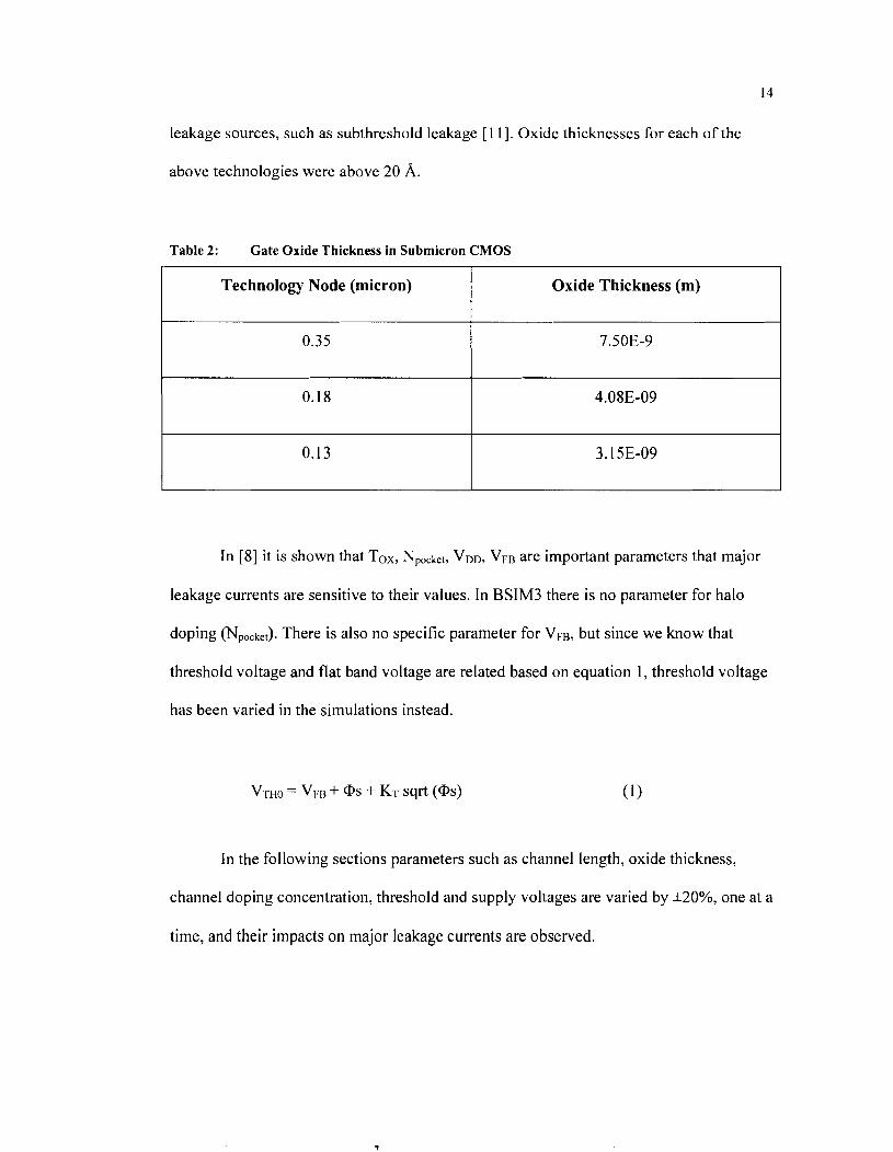
Table 2: Gate Oxide Thickness in Submicron CMOS
In [8] it is shown that Tox, Npocket, VDD, VFB are important parameters that major
leakage currents are sensitive to their values. In BSIM3 there is no parameter for halo
doping (Npocket). There is also no specific parameter for VFB, but since we know that
threshold voltage and flat band voltage are related based on equation 1, threshold voltage
has been varied in the simulations instead.
Technology Node (micron)
0.35
0.18
0.13
In the following sections parameters such as channel length, oxide thickness,
channel doping concentration, threshold and supply voltages are varied by *20%, one at a
time, and their impacts on major leakage currents are observed.
Oxide Thickness (m)
7.50E-9
4.08E-09
3.15E-09
15
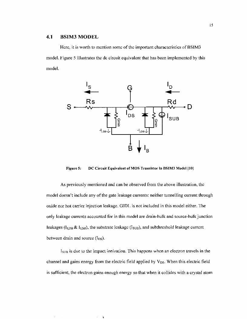
4.1 BSIM3 MODEL
Here, it is worth to mention some of the important characteristics of BSIM3
model. Figure 5 illustrates the dc circuit equivalent that has been implemented by this
model.
Rs I S
Rd n D IDS G> lSUB
I
Figure 5: DC Circuit Equivalent of MOS Transistor in BSIM3 Model [lo]
As previously mentioned and can be observed from the above illustration, the
model doesn't include any of the gate leakage currents: neither tunnelling current through
oxide nor hot carrier injection leakage. GIDL is not included in this model either. The
only leakage currents accounted for in this model are drain-bulk and source-bulk junction
leakages ( I j , p ~ & I j , s~) , the substrate leakage (ISUB), and subthreshold leakage current
between drain and source (IDS).
IsUB is due to the impact ionization. This happens when an electron travels in the
channel and gains energy from the electric field applied by V D ~ . When this electric field
is sufficient, the electron gains enough energy so that when it collides with a crystal atom
16
it generates an electron-hole pair. The generated electron will move towards drain, which
has positive potential while the hole will move towards bulk, which is at lower potential.
On their way they can collide with more crystal atoms and generate more electron-hole
pairs, leading to avalanche multiplication of electron-hole pairs.
A summary of terminal currents and their relationships for this model is outlined
in the following equations [lo]:
Based on the above equations, the relationship between components of leakage
current at drain, source, and bulk in BSIM3 model can be understood.
4.2 0.35-micron Technology
For this simulation circuit of Figure 4 was utilized. WIL of transistor was 0.810.35
with VD, at 3.3 V.
4.2.1 I-V Characteristics
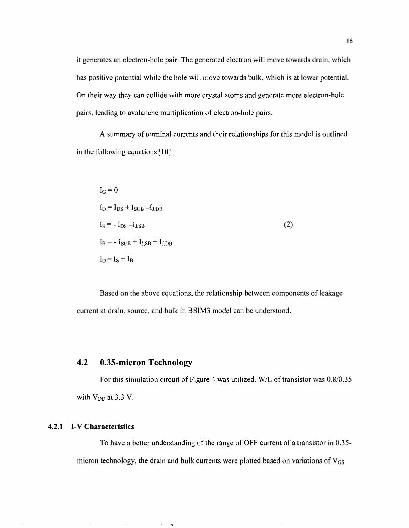
To have a better understanding of the range of OFF current of a transistor in 0.35-
micron technology, the drain and bulk currents were plotted based on variations of VGS
for several VBS values. For this simulation VDD was set at 3.3V while VGS was swept
from 0 to 5V with steps of 25mV and VBS was varied from 0 to -1.W by -0.W steps.
The result for drain and bulk currents are illustrated in Figure 6 and Figure 7.
As it can be observed from Figure 6, the OFF current of this transistor is in the
range of several PA. As the bulk-source voltage decreases, higher voltage needs to be
applied to the gate-source in order to turn the transistor on (body effect).
ID-V Characteristics
VGS (V)
1 2 3
1 E-10
I E-I I --
--- - - - - - - - -- -
Figure 6: ID-V Characteristics of NMOS (W/L=0.8/0.35, VDD=3.3V)
Is-V Characteristics v~~ (v)
0 1 2 3 4 5
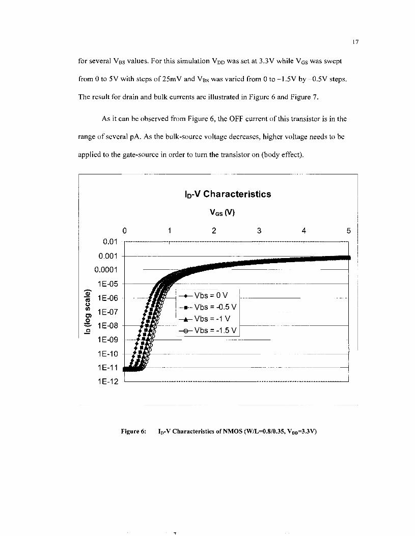
Figure 7: Is-V Characteristics of NMOS (WIL=0.8/0.35, VDD=3.3V)
If we assume that the junction currents are minute and I J , ~ s ) , then the bulk
current is same as the substrate current (Figure 5). When VDs is large, the transistor
operates in saturation. The electric field between the gate-drain terminals, close to where
the channel pinches off, is large and therefore the substrate current due to impact
ionization is large.
The bell shape graph of Figure 7 indicates that there are two factors influencing
the value of impact ionization. One is the amount of the electron carriers (channel
19
current) and the second factor is the gate-drain junction electric field. When VGS is small
the channel is not strongly inverted, therefore the number of electrons present in the
channel are small and hence the substrate current is small too. As VGS increases, the
inversion gets stronger and the number of electrons that can initiate impact ionization
increases. This results in an increase in the bulk current (becomes more negative).
However this doesn't continue forever. After VGS passes a certain value (VDs
remains constant) the voltage drop across the saturated region decreases. This means that
the electric field and hence the amount of impact ionization decreases. If VGs - VDs > VT
then the transistor starts operating in the linear region and the bulk current goes back to
very small values [lo].

4.2.1.1 A Case Study
A transistor with aspect ratio of 10 (W/L= 3.5/0.35), VDD = 1.5V was tested and
its bulk and drain currents measured [12]. Ves was varied from 0 to -1 SV. Using
CadenceTM tool the simulation in the same operating conditions was performed. The
following graphs show the similarities and differences between measurement and
simulation results.
Figure 8: Measurement of Bulk Current vs. VGSat Various VBS, VDD=l.SV I121
le-V characterisitcs- simulation
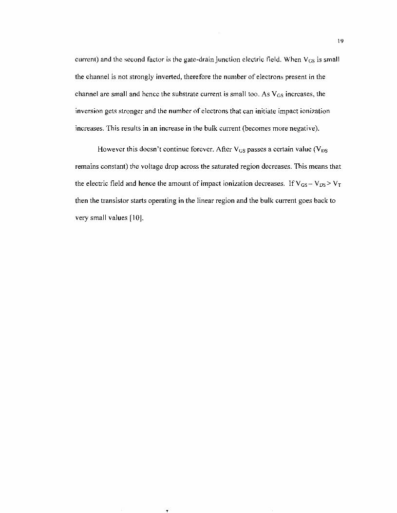
Figure 9: Simulation of Bulk Current vs. VGS at Various VBS, VDD=l.SV
Comparing the measured and simulated data (Figure 8, Figure 9), it can be
observed that in simulation the maximum absolute value of bulk current is around 70pA
and the peak value has happened between 0.75 to 1.025V of VGS. While in actual
measurement the bulk current has a range between 35 to 80 pA and the peak has occurred
between 0.8-1.1V of VGS. Decrease of -5OpA of bulk current for different values of VBS
can be due to other leakage and parasitic sources that are not accounted for in the
simulation model file.
The following graphs compare the test and simulation results for drain current.

Figure 10: Measurement - Drain Current vs. VGsat Various VBS, VDD=l.SV 1121

IuV Characteristics
VGS (V)
0 0.5 1 1.5
Figure 11: Simulation - Drain Current vs. VGS at Various VBS, VDD=1.5V

- -- --
I,-V (Simulation vs. Measurement)
- --
Figure 12: Drain Current Comparison for VBs=O, VDD=1.5V
As can be observed from the Figure 12, there is a 40-60% difference between the
simulation and measurement results in subthreshold region, but this difference becomes
less as the transistor enters the linear region of operation.
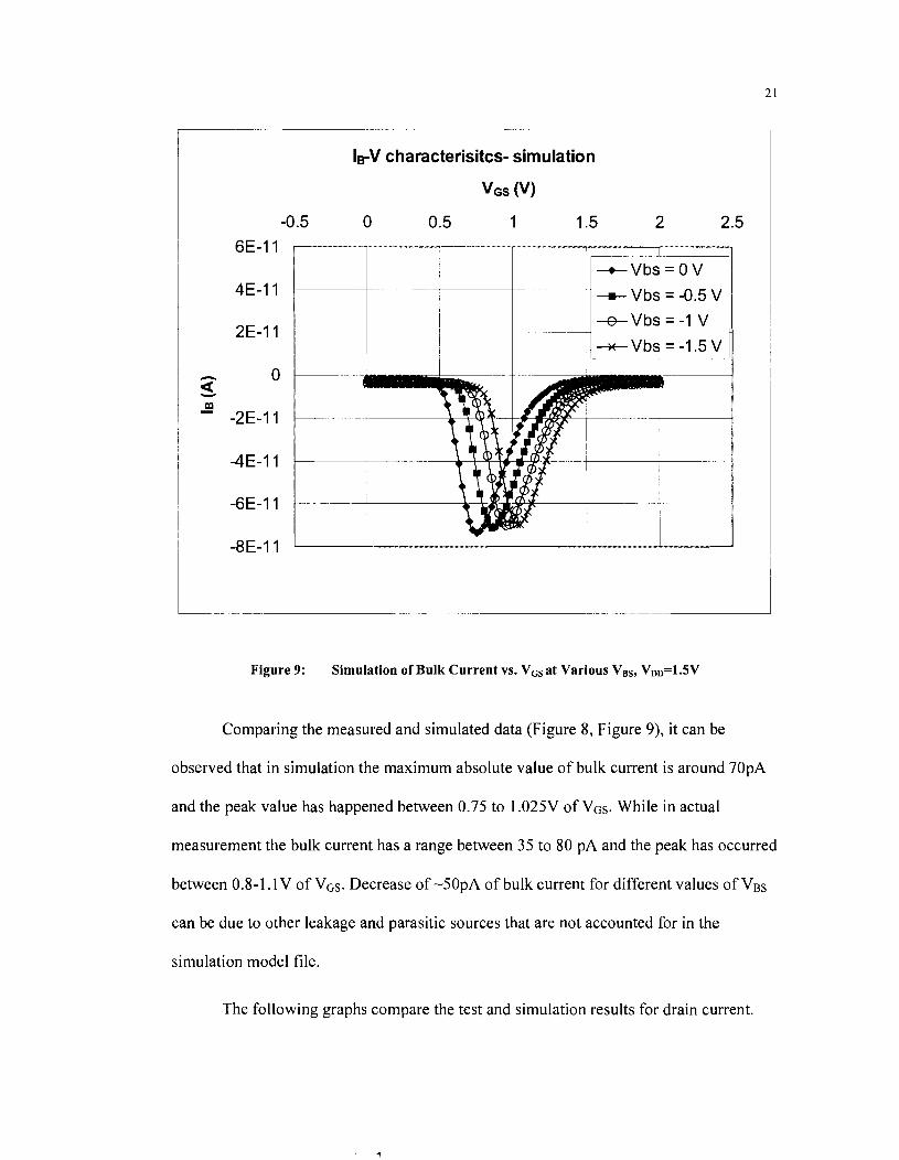
Figure 13 compares the measured and simulated results for the bulk current.
- - --
Is-V (Simulation vs. Measurement)
v~~ (v) 0 0.5 1 1.5 2 2.5
Figure 13: Bulk Current Comparison for Vss=O, VDD=1.5V
It can be observed that the measured bulk current does not follow the simulation
as closely as the drain current does. This can be due to other factors that are not
accounted for in the model file.
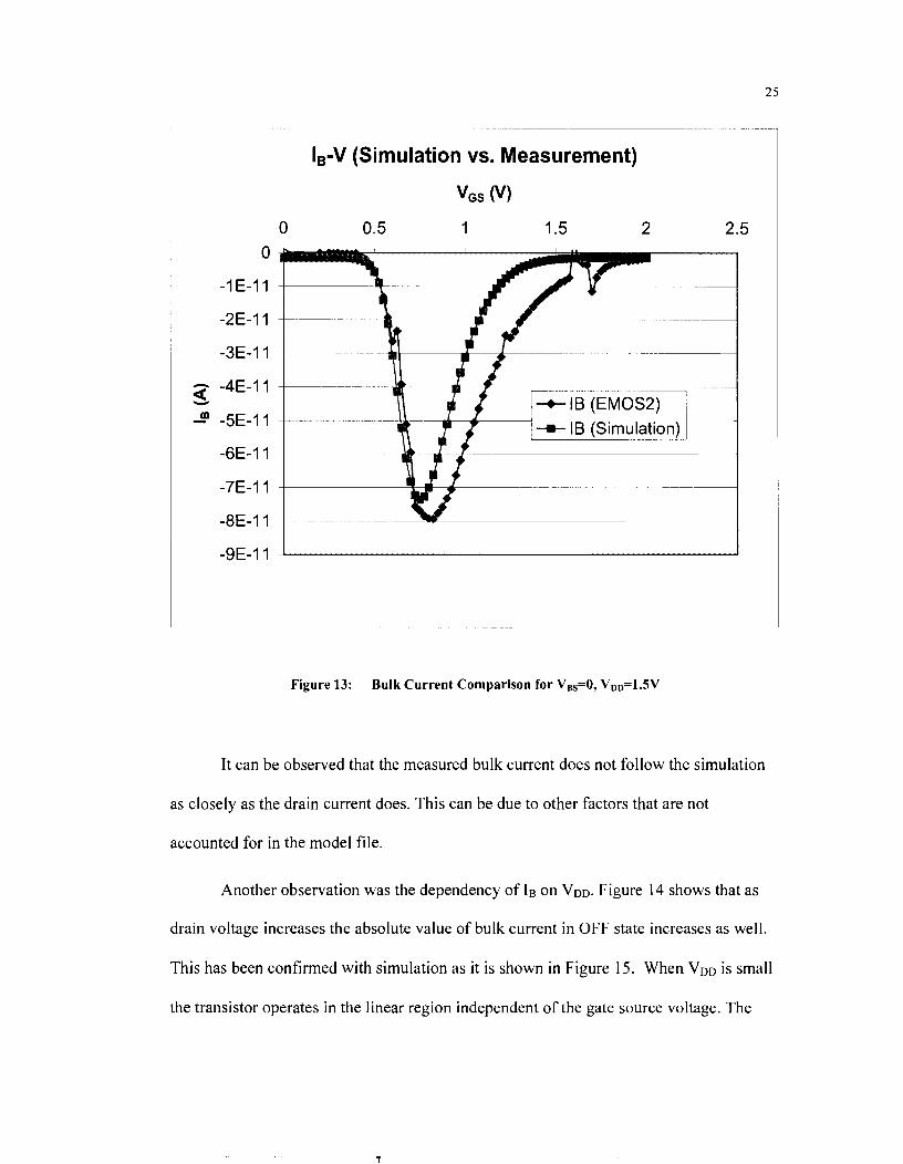
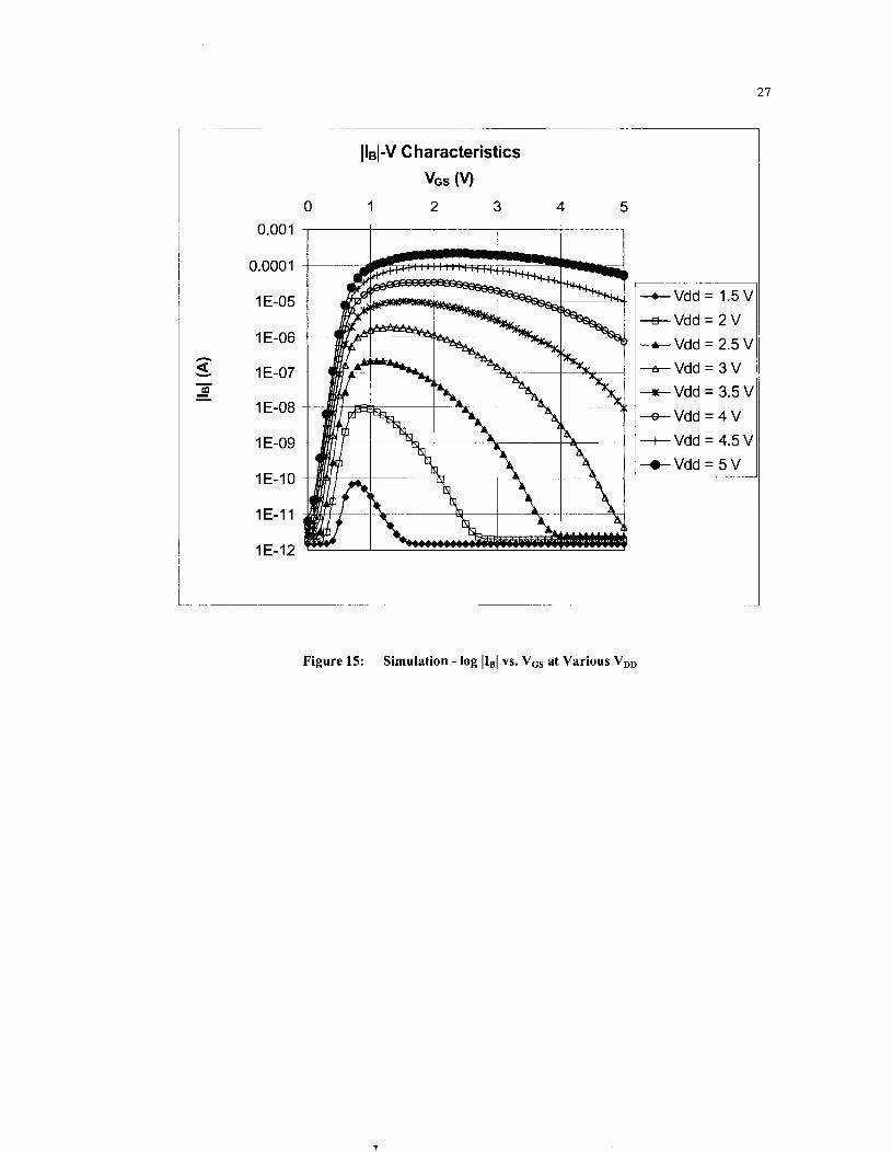
Another observation was the dependency of IB on VDD. Figure 14 shows that as
drain voltage increases the absolute value of bulk current in OFF state increases as well.
This has been confirmed with simulation as it is shown in Figure 15. When VDD is small
the transistor operates in the linear region independent of the gate source voltage. The
26
applied electric field close to drain is small and hence the amount of impact ionization is
almost zero. As VDD increases the transistor enters the saturation region. The channel
pinches off and the electric field between gate and drain becomes large and so does the
substrate current (impact ionization) [ I 01.
Figure 14: Measurement - log lIBl VS. Vcs at Various VDD [12]
Ilsl-V Characteristics
VGS (V)
0 1 2 3 4 5
0.001 1 I I
1 I
- --
Figure 15: Simulation - log 1111 vs. Vcc at Various Vnn
- --
-Vdd = 1.5V
*Vdd=2V
-A- Vdd = 2.5 V
*Vdd= 3 V
+Vdd = 3.5 \,
*Vdd=4V
+ Vdd = 4.5 V
+Vdd = 5 V
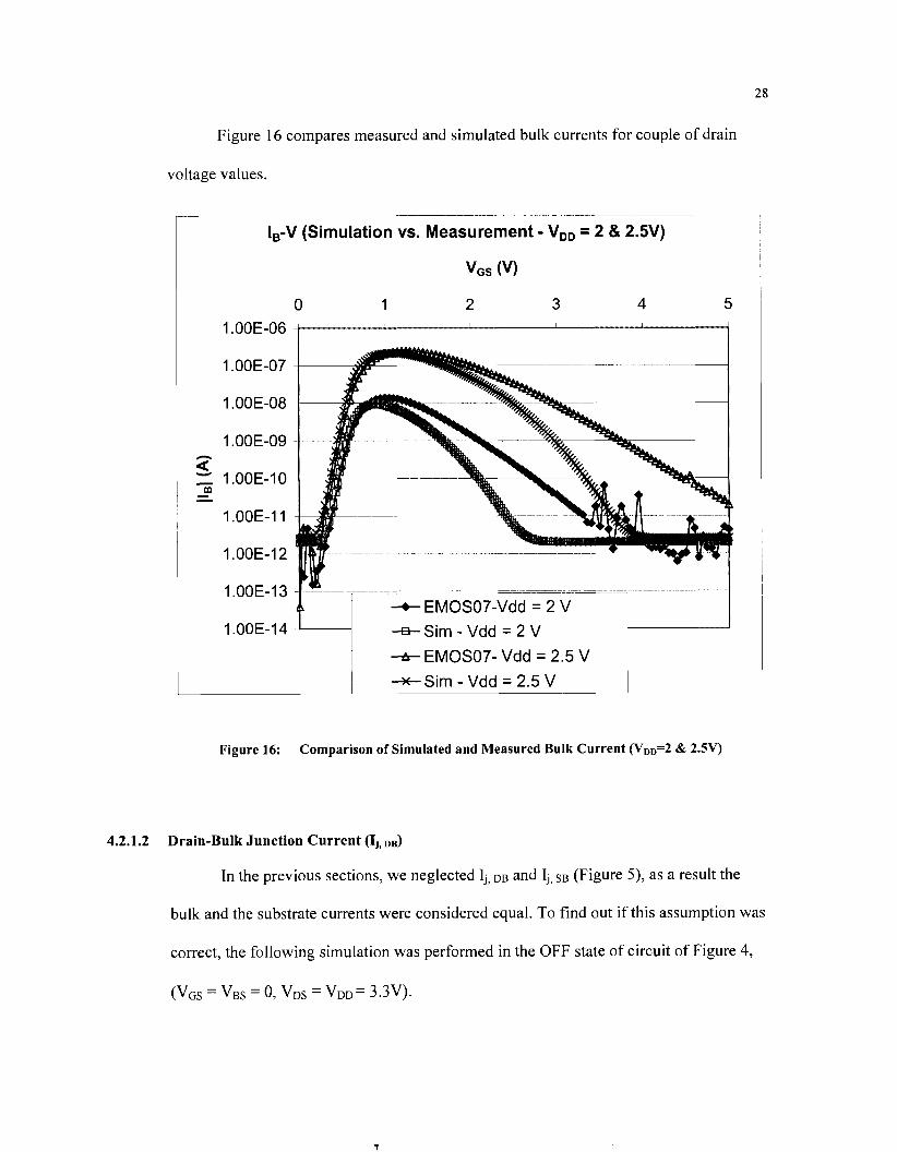
Figure 16 compares measured and simulated bulk currents for couple of drain
voltage values.
I,-V (Simulation vs. Measurement - VDD = 2 & 2.5V)
v~~ (v)
0 1 2 3 4 5
1 4 EMOSO7- Vdd = 2.5 V 1
Figure 16: Comparison of Simulated and Measured Bulk Current (VDD=2 & 2.W)
4.2.1.2 Drain-Bulk Junction Current (Ij, DB)
In the previous sections, we neglected Ij, DB and Ij, s~ (Figure 5), as a result the
bulk and the substrate currents were considered equal. To find out if this assumption was
correct, the following simulation was performed in the OFF state of circuit of Figure 4,
(VGS = VBS = 0, VDS = VDD = 3.3V).
29
The drain diffusion area (AD) is one of the transistor parameters. Its default value
for 0.35-micron technology is:
AD = 1 x Width of transistor (pnZ)
This value was increased until a significant change in the bulk current was
observed (in the range of PA). By increasing the drain area by lo4, an increase of 2.02pA
was detected in the bulk current.
IB I = -3.347pA Default value at AD = 1 x 3.5 @m2)
1 ~ 2 = -5.369pA New value at AD = 1 x 3.5 x lo4 @m2)
The conclusion drawn was that Ij, DB is about 4 orders of magnitude less than the bulk
current, and therefore with AD at its default value, Ij, DB will approximately be equal to:
II,, D B I 3.347E-16 A (or 334.7 aA)
Therefore, our first assumption to neglect the reverse-bias p-n junction currents in respect
to the bulk current is justified.

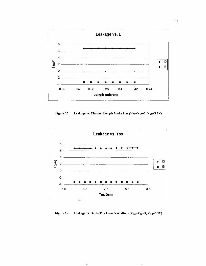
4.2.2 Channel Length Variations
In this section we observe the effect of channel length variation on transistor
leakage currents. The circuit was in the OFF state (VGS = 0, VBS = 0, VDD = 3.3V). L was
varied by +20%. The default value was 0.35 micron. Figure 17 illustrates drain and bulk
leakage. It has been observed that drain current varies about 0.3% while bulk current
stays almost constant over the entire range.
4.2.3 Oxide Thickness Variations
The default value for Tox of this model transistor is 7.5E-9 m. Oxide thickness
was varied over a range of *20% and the leakage currents were measured. Figure 18
illustrates the results. The outcome shows that for drain current *20% variation in Tox
only changes it by 2.25% and 1.3% respectively and for bulk current by 0.21% and
0.12% respectively.
4.2.4 Channel Doping Variations
The default value for channel doping is 2.3579E+37 ~ m - ~ . This value was changed
by *20% and the drain and bulk currents were plotted. The result showed that drain
current varied by 0.8% and % 0.9 respectively while the bulk current changed by % 0.09.
Figure 19 illustrates this.
- - --
Leakage vs. L
Length (micron)
Leakage vs. Tox
Figure 17: Leakage vs. Channel Length Variations (VGS=VBS=O, VDD=3.3V
5.5 6.5 7.5 8.5 9.5
Tox (nm)
Figure 18: Leakage vs. Oxide Thickness Variations (VGS=VBS=O, VDD=3.3V)

Leakage vs. NCH
Figure 19: Leakage vs. Channel Doping Variations (VGS=VBS=O, VDD=3.3V)
-2
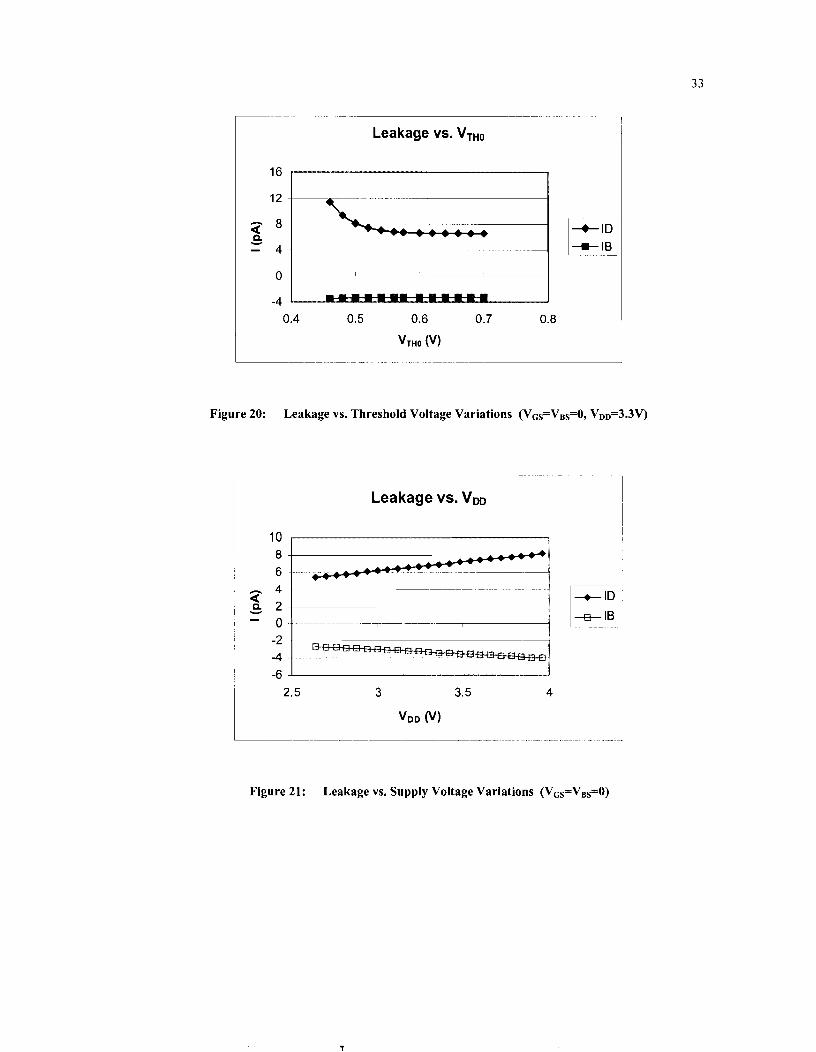
4.2.5 Threshold Voltage Variations
As described earlier, the goal was to vary flat band voltage, but since there is no such
parameter available in the model file, and since it is known that flat band voltage and
threshold voltage are related (Equation l), VTHo was varied over + 20%. The default
value for threshold voltage is 0.574607 V. The result showed that drain current was
varied by 2.5% and 68% and bulk current by 0.24% and 6% respectively. Figure 20
illustrates this observation.
- - - -. - -- -
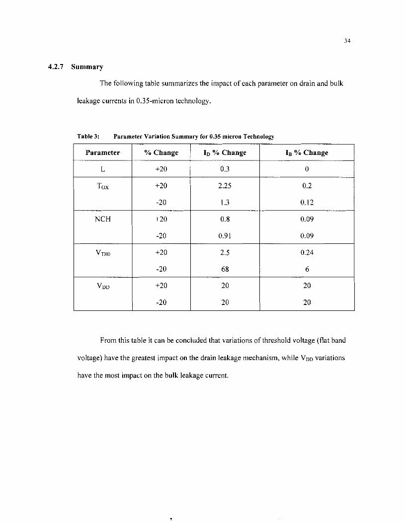
4.2.6 VDD Variations
The value of VDD was originally at 3.3 V. Varying it by +20% caused both the drain and
bulk current to vary by 20'36, as illustrated in Figure 2 1.
-4 1.50E+17 2.00E+17 2.50E+17 3.00E+17
NCH (cm-3)
Leakage vs. VTHo
Figure 20: Leakage vs. Threshold Voltage Variations (VGS=VBS=O, VDD=3.3V)
Leakage vs. Vm
Figure 21: Leakage vs. Supply Voltage Variations
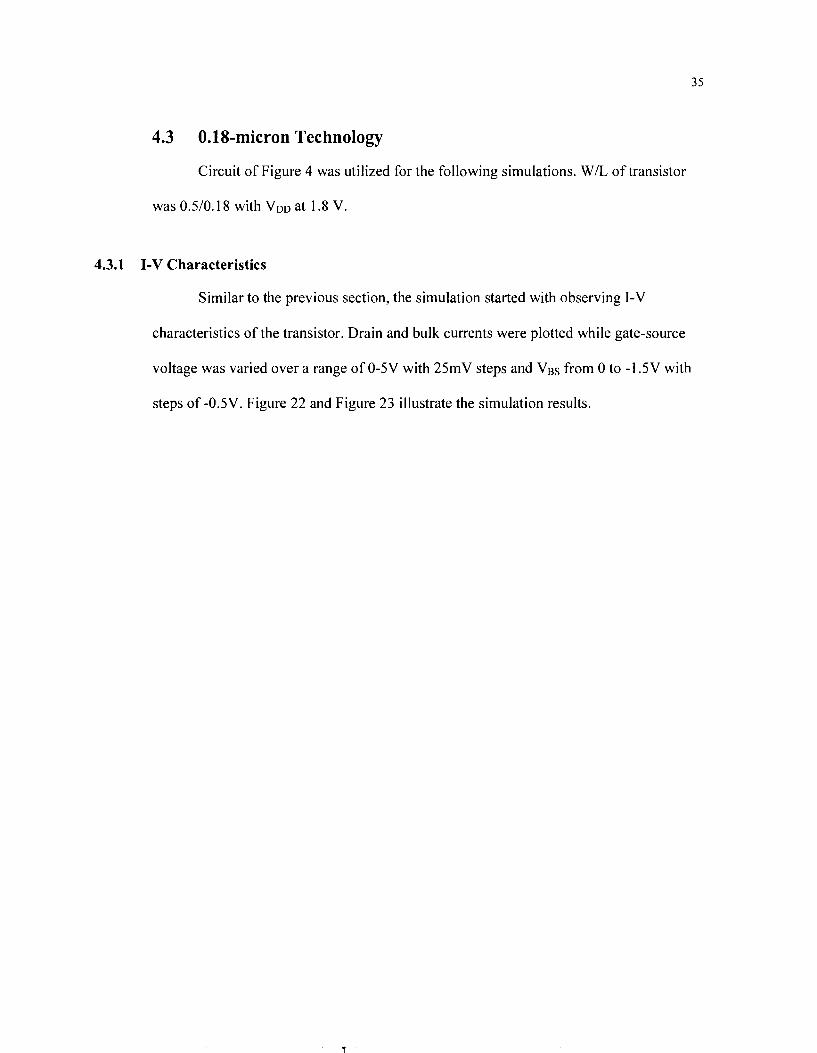
4.2.7 Summary
The following table summarizes the impact of each parameter on drain and bulk
leakage currents in 0.35-micron technology.
Table 3: Parameter Variation Summary for 0.35 micron Technology
Tox
% Change 1 1. % Change Ie % Change
From this table it can be concluded that variations of threshold voltage (flat band
voltage) have the greatest impact on the drain leakage mechanism, while VDD variations
have the most impact on the bulk leakage current.
4.3 0.18-micron Technology
Circuit of Figure 4 was utilized for the following simulations. WIL of transistor
was 0.510.1 8 with VDD at 1.8 V.
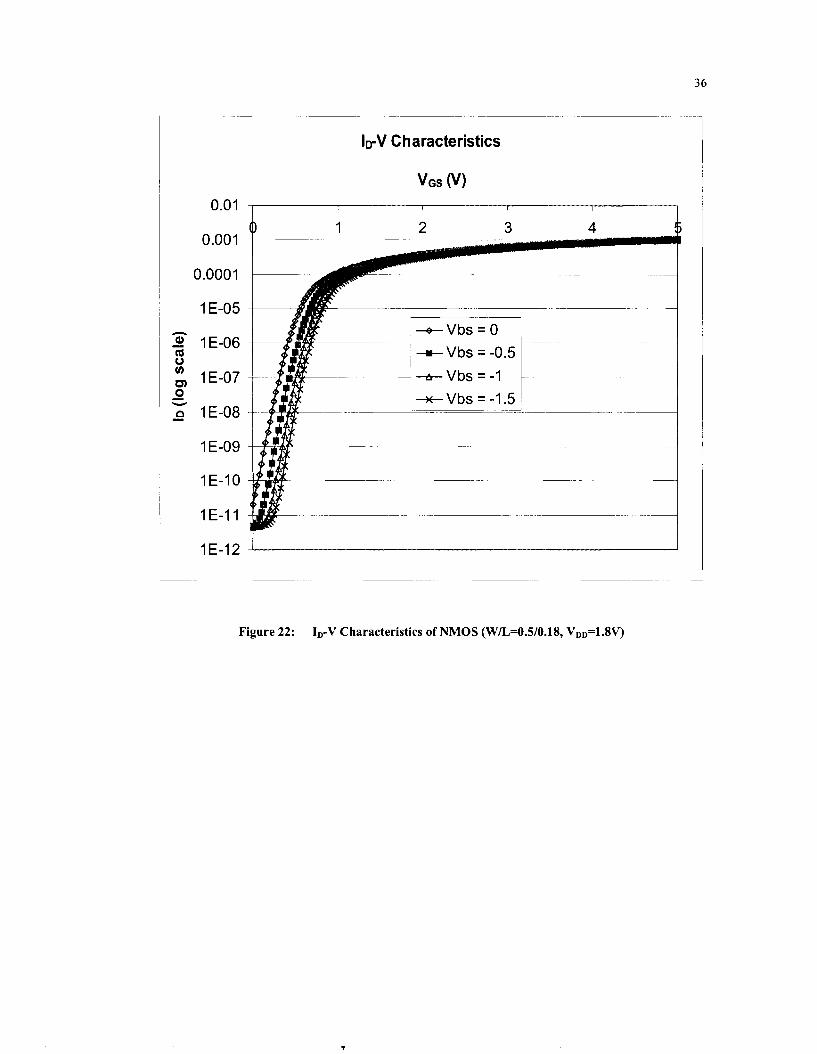
4.3.1 I-V Characteristics
Similar to the previous section, the simulation started with observing I-V
characteristics of the transistor. Drain and bulk currents were plotted while gate-source
voltage was varied over a range of 0-5V with 25mV steps and Vss from 0 to -1 .W with
steps of -0.W. Figure 22 and Figure 23 illustrate the simulation results.
IuV Characteristics
VGS (v)
Figure 22: ID-V Characteristics of NMOS (W/L=0.5/0.18, VDD=1.8V)
I& Characteristics
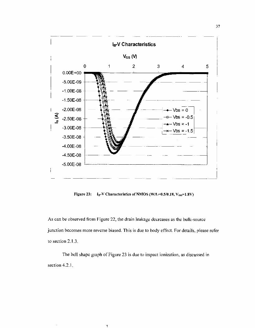
Figure 23: IB-V Characteristics of NMOS (W/L=0.5/0.18, VDD=1.8V)
As can be observed from Figure 22, the drain leakage decreases as the bulk-source
junction becomes more reverse biased. This is due to body effect. For details, please refer
to section 2.1.3.
The bell shape graph of Figure 23 is due to impact ionization, as discussed in
section 4.2.1,
4.3.2 Channel Length Variations
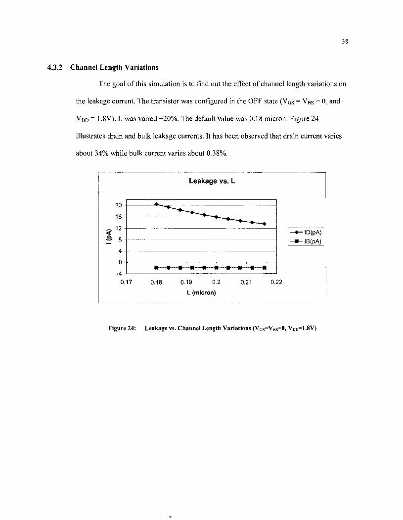
The goal of this simulation is to find out the effect of channel length variations on
the leakage current. The transistor was configured in the OFF state (VGS = VBS = 0, and
VDD = 1.8V). L was varied +20%. The default value was 0.1 8 micron. Figure 24
illustrates drain and bulk leakage currents. It has been observed that drain current varies
about 34% while bulk current varies about 0.38%.
Leakage vs. L
0.17 0.18 0.19 0.2 0.21 0.22
L (micron) -- -- -- - --
Figure 24: Leakage vs. Channel Length Variations (VGs=Vss=O, VDD=1.8V)
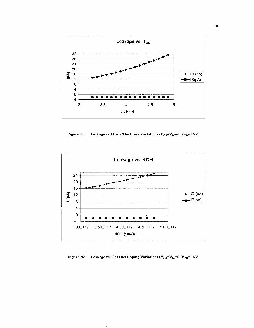
4.3.3 Oxide Thickness Variations
The default value for Tox of this model transistor is 4.08E-9 m. Oxide thickness
was varied over a range of +20% and the leakage currents were plotted. Figure 25
illustrates the results. It shows that +20% variation in Tox changes drain current by 53%
and 35% and the bulk current by 0.66% and 0.44% respectively.
4.3.4 Channel Doping Variations
The default value for channel doping is 3.9E+17 ~ m - ~ . +20% variation of NCH changed
the drain current by 22% and 20% and the bulk current by 0.27% and 0.22% respectively.
Figure 26 illustrates this.
4.3.5 Threshold Voltage Variations
The goal was to vary flat band voltage, but since there is no such parameter available in
the model file, and since it is known that flat band voltage and threshold voltage are
related (Equation l), VTHo was varied over a range of +20%. The default value for
threshold voltage for this technology is 0.4736658 V. The drain current changed by 78%
and 1185% and the bulk current by 0.93% and 14% respectively, as illustrated in Figure
4.3.6 VDD Variations
The original value of VDD was 1.8 V. Varying it by +20% caused the drain current to
change by 15% and 14% respectively and the bulk current by 22% and 20% respectively,
as illustrated in Figure 28.
-
Figure 25: Leakage vs. Oxide Thickness Variations (VGs=VBs=O, VDD=l.8V)
Leakage vs. NCH
Figure 26: Leakage vs. Channel Doping Variations (VGS=VBS=O, VDD=1.8V
Leakage vs. VTHo
Figure 27: Leakage vs. Threshold Voltage Variations
Leakage vs. VDD
Figure 28: Leakage vs. Supply Voltage Variations (VGS=VBS=O)
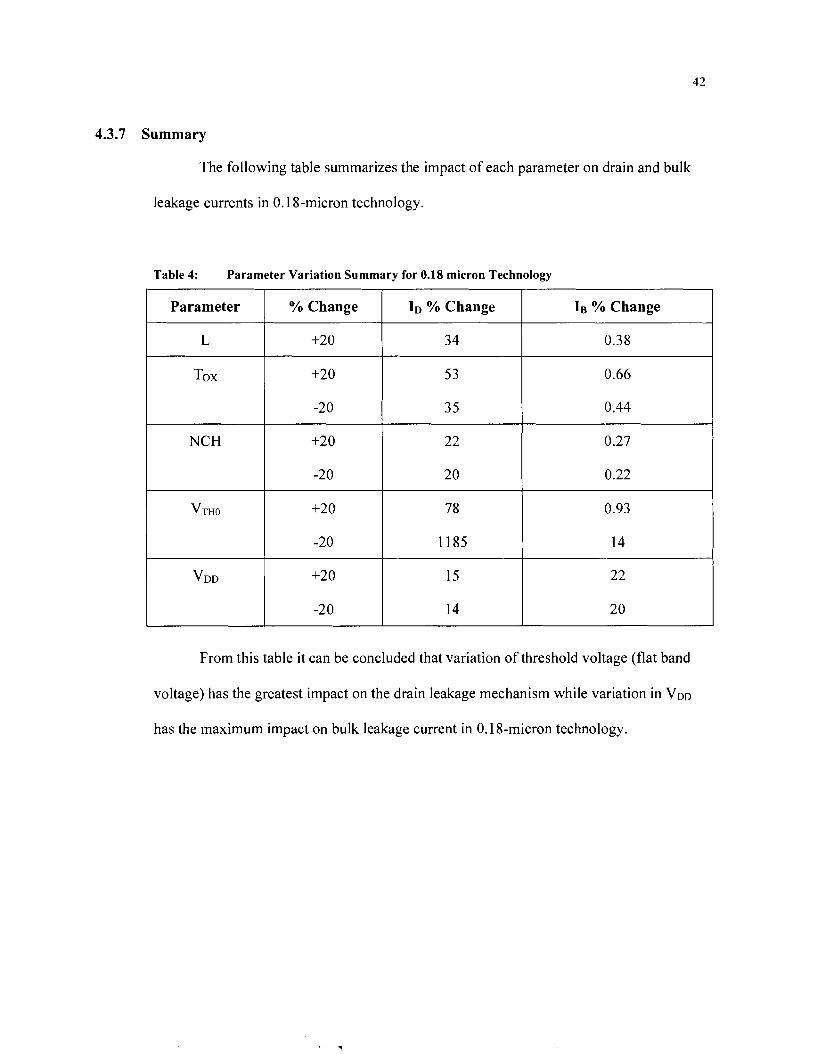
4.3.7 Summary
The following table summarizes the impact of each parameter on drain and bulk
leakage currents in 0.18-micron technology.
Table 4: Parameter Variation Summary for 0.18 micron Technology
I Parameter % Change I 1. % Change I Is % Change
From this table it can be concluded that variation of threshold voltage (flat band
voltage) has the greatest impact on the drain leakage mechanism while variation in VDD
has the maximum impact on bulk leakage current in 0.18-micron technology.

4.4 0.13-micron Technology
For this simulation circuit of Figure 4 was utilized. WIL of transistor was 0.610.1 3
and VDD = 1.2V.
4.4.1 I-V Characteristics
To have a better understanding of the range of OFF current of the transistor, the
drain and bulk currents of the transistor were plotted based on various gate-source
voltages and bulk-source voltages. VGS was swept from 0 to 1.2V with 25mV steps, and
VBS was varied between 0 to -0.75V with -0.25V steps. VDD was at 1.2V. Figure 29 and
Figure 30 illustrate the results obtained from these simulations.
I,-V Characteristics
Figure 29: ID-V Characteristics of NMOS (W/L=0.6/0.13, VDD=l.2v)
As it can be observed from Figure 29, the OFF current of this transistor decreases as the
bulk-source voltage becomes more negative (body effect). Also the value of the drain
current in subthreshold region is more than those of the previous two technologies, which
shows the impact of transistor scaling on leakage.
Figure 30 illustrates the bulk current of this transistor for the same VGS and Vss
values.

lev Characteristics
Figure 30: IB-V Characteristics of NMOS (W/L=0.6/0.13, VDD=1.2V)
Unlike the previous two technology nodes, the bulk current doesn't have a bell
shape graph in 0.13-micron technology. It may be due to lack of accurate transistor
modeling in the model file provided by Canadian Microelectronic Corporation (CMC).
This area requires more investigation.
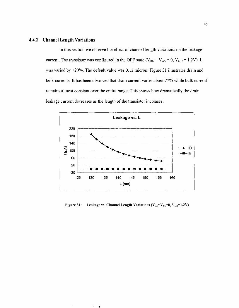
4.4.2 Channel Length Variations
In this section we observe the effect of channel length variations on the leakage
current. The transistor was configured in the OFF state (VBS = VGS = 0, VDD = 1.2V). L
was varied by +20%. The default value was 0.13 micron. Figure 3 1 illustrates drain and
bulk currents. It has been observed that drain current varies about 77% while bulk current
remains almost constant over the entire range. This shows how dramatically the drain
leakage current decreases as the length of the transistor increases.
Leakage vs. L
Figure 31: Leakage vs. Channel Length Variations (VGs=VBs=O, VDD=1.2V)
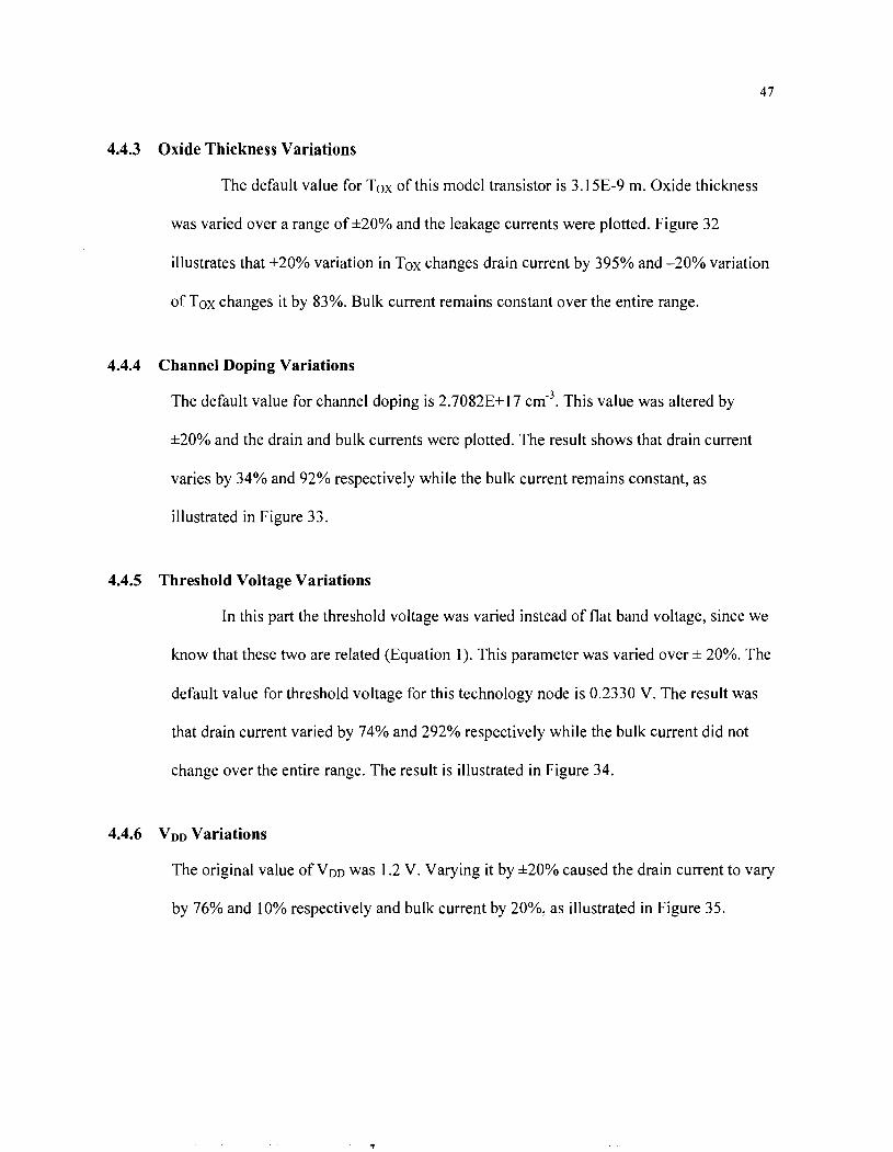
4.4.3 Oxide Thickness Variations
The default value for Tox of this model transistor is 3.15E-9 m. Oxide thickness
was varied over a range of *20% and the leakage currents were plotted. Figure 32
illustrates that +20% variation in Tox changes drain current by 395% and -20% variation
of Tox changes it by 83%. Bulk current remains constant over the entire range.
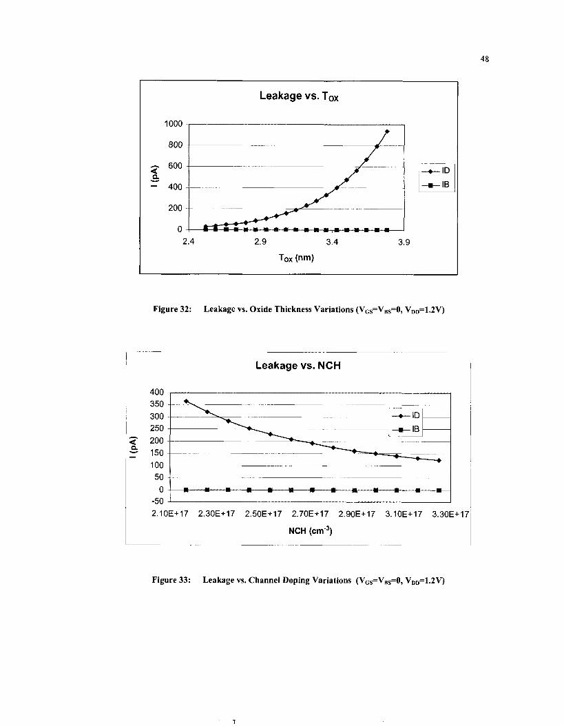
4.4.4 Channel Doping Variations
The default value for channel doping is 2.7082E+l7 ~ m - ~ . This value was altered by
*20% and the drain and bulk currents were plotted. The result shows that drain current
varies by 34% and 92% respectively while the bulk current remains constant, as
illustrated in Figure 33.
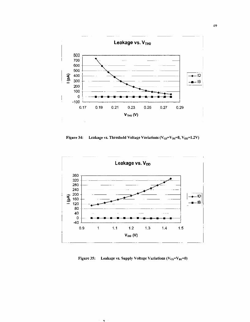
4.4.5 Threshold Voltage Variations
In this part the threshold voltage was varied instead of flat band voltage, since we
know that these two are related (Equation 1). This parameter was varied over * 20%. The
default value for threshold voltage for this technology node is 0.2330 V. The result was
that drain current varied by 74% and 292% respectively while the bulk current did not
change over the entire range. The result is illustrated in Figure 34.
4.4.6 VDD Variations
The original value of VDD was 1.2 V. Varying it by *20% caused the drain current to vary
by 76% and 10% respectively and bulk current by 20%, as illustrated in Figure 35.
Leakage vs. Tox
2.9 3.4
Tox (nm)
Figure 32: Leakage vs. Oxide Thickness Variations (VGs=Vss=O, VDD=l.2V)
Leakage vs. NCH
Figure 33: Leakage vs. Channel Doping Variations (VGS=V~S=O, VDD=l.2V)
Leakage vs. VTHo
Figure 34: Leakage vs. Threshold Voltage Variations (VGS=VBS=O, VDD=1.2V)
Leakage vs. VDD
Figure 35: Leakage vs. Supply Voltage Variations (Vcs=VBs=O)
4.4.7 Summary
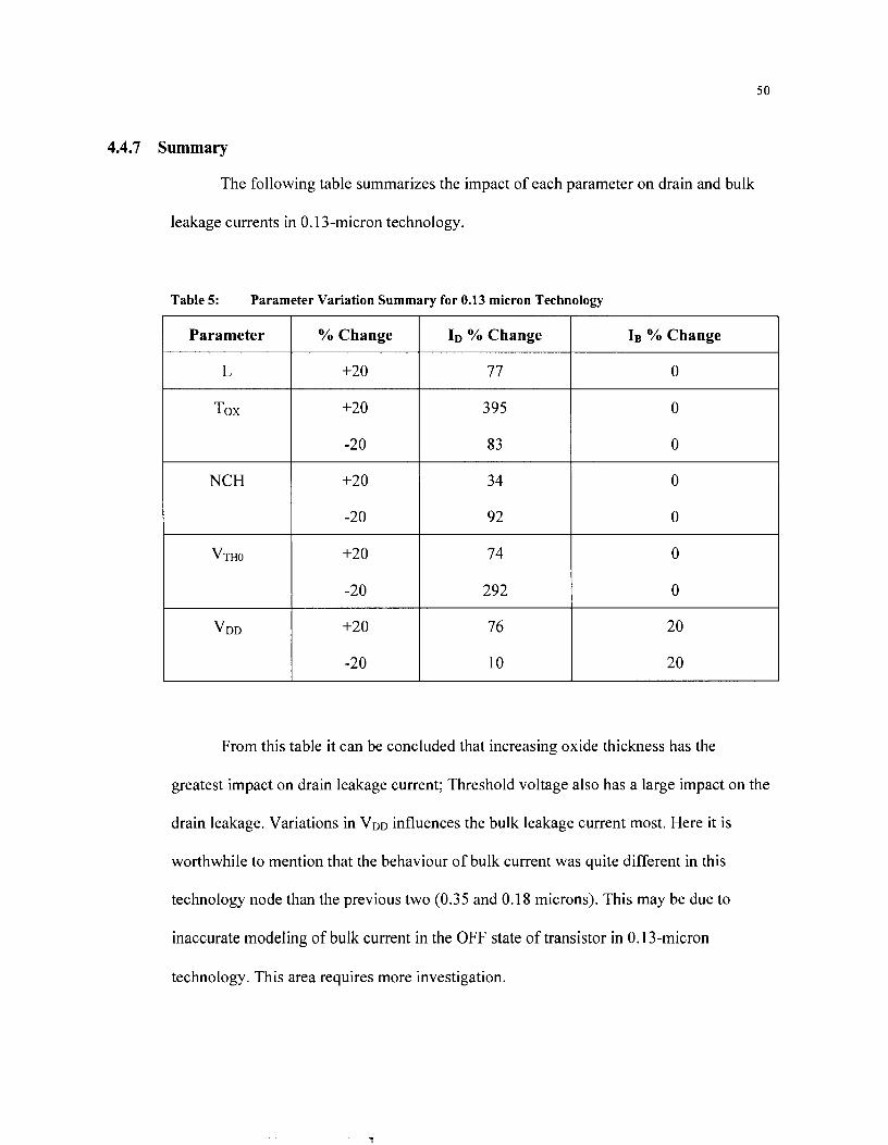
The following table summarizes the impact of each parameter on drain and bulk
leakage currents in 0.13-micron technology.
Table 5: Parameter Variation Summary for 0.13 micron Technology
Parameter 1 % Change I 1. % Change I Ig % Change
Tox
NCH
From this table it can be concluded that increasing oxide thickness has the
greatest impact on drain leakage current; Threshold voltage also has a large impact on the
drain leakage. Variations in VDD influences the bulk leakage current most. Here it is
worthwhile to mention that the behaviour of bulk current was quite different in this
technology node than the previous two (0.35 and 0.1 8 microns). This may be due to
inaccurate modeling of bulk current in the OFF state of transistor in 0.13-micron
technology. This area requires more investigation.
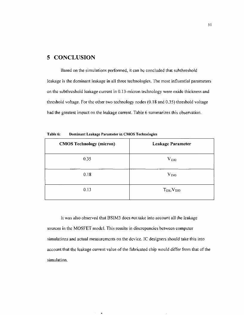
5 CONCLUSION
Based on the simulations performed, it can be concluded that subthreshold
leakage is the dominant leakage in all three technologies. The most influential parameters
on the subthreshold leakage current in 0.1 3-micron technology were oxide thickness and
threshold voltage. For the other two technology nodes (0.1 8 and 0.35) threshold voltage
had the greatest impact on the leakage current. Table 6 summarizes this observation.
Table 6: Dominant Leakage Parameter in CMOS Technologies
It was also observed that BSIM3 does not take into account all the leakage
sources in the MOSFET model. This results in discrepancies between computer
simulations and actual measurements on the device. IC designers should take this into
account that the leakage current value of the fabricated chip would differ from that of the
simulation.
CMOS Technology (micron)
0.35
Leakage Parameter
VTHO
5 2
This research project can be a starting point for identifying the IDDa values for
building blocks of more complex integrated circuits. Same methodology can be utilized
to simulate larger functional blocks in CMOS. Simulated leakage components can be
efficiently controlled using such BSIM3 model parameters as VTHo and To*.
As scaling in CMOS technology continues, leakage current and static power
dissipation will increase. Many leakage reduction methods have been developed, but still
more research needs to be done in this field. Carefully designing the integrated circuits
and utilizing the circuit level techniques can effectively control leakage current
mechanisms in submicron CMOS technologies.

6 REFERENCES
R. Kumar, C.P. Ravikumar, "Leakage power estimation for deep submicron circuits in an ASIC design environment", Design Automation Conference on VLSI Design, ASP-DAC 2002, 7-1 1 Jan. 2002, pp. 45 - 50.
K. Roy, "Leakage Tolerant Circuits, Sub-threshold Logic", Electrical and Computer Engineering Purdue University http://dynamo.ecn.purdue.edu/-vlsi/ courses/ee695kr/s200l/ee695kr notesllecture4-1eakaae.PDF (Accessed Nov 9, 2004)
P. Maxwell, P. O'Neill, R. Aitken, R. Dudley, N. Jaarsma, M. Quach, D. Wiseman, "Current ratios: a self-scaling technique for production IDDQ testing", International Test Conference, 3-5 Oct. 2000, pp. 1 148 - 1 156.
A. Agarwal, L. He, et.al, "Leakage Modeling and Reduction", http://eda.ee.ucla.edu/EE20 1 A-04Sprina/leakage pres.ppt (Accessed Nov 13, 2004).
K. Roy, S. Mukhopadhyay, H. Mahmoodi-Meimand, "Leakage current mechanisms and leakage reduction techniques in deep-sub micrometer CMOS circuits", IEEE, Vol. 91, No. 2, Feb. 2003, pp. 305 - 327.
0 . Semenov, A. Pradzynski, M. Sachdev, "Impact of gate induced drain leakage on overall leakage of submicrometer CMOS VLSI circuits", IEEE Transactions on Semiconductor Manufacturing, Vol. 15, No. 1, Feb. 2002, pp. 9 - 18.
C.H. Kim, K. Jae-Joon, S. Mukhopadhyay, K. Roy, "A forward body-biased-low- leakage SRAM cache: device and architecture considerations", International Symposium on Low Power Electronics and Design, ISLPED '03., 25-27 Aug. 2003, pp. 6 - 9.
S. Mukhopadhyay, K. Roy, "Modeling and estimation of total leakage current in nano-scaled-CMOS devices considering the effect of parameter variation", International Symposium on Low Power Electronics and Design, ISLPED '03,25- 27 Aug. 2003, pp. 172 - 175.
A. Srivastava, R. Bai, , D. Blaauw, D. Sylvester, "Modeling and analysis of leakage power considering within-die process variations", International Symposium on Low Power Electronics and Design, ISLPED '02, 12-14 Aug. 2002, pp. 64 - 67.
[lo] W. Liu, "MOSFET Models for SPICE Simulation Including BSIM3V3 and BSIM4", ISBN: 0-471-39697-4.
[ l 11 L. Dongwoo, D. Blaauw, D. Sylvester, "Gate oxide leakage current analysis and reduction for VLSI circuits", Transactions on Very Large Scale Integration (VLSI) Systems, IEEE, Vol. 12, No. 2, Feb. 2004, pp. 55 - 166.
[12] M. Syrzycki, private communication, VLSI lab-SFU Engineering School.