multivalued logic for reduced pin count and multi-site soc testing baohu li and vishwani d. agrawal...
TRANSCRIPT

Multivalued Logic for Reduced
Pin Count and Multi-Site SoC Testing
Baohu Li and Vishwani D. AgrawalAuburn University, ECE Dept., Auburn, AL 36849,
USA
24th IEEE North Atlantic Test WorkshopJohnson City, NY, May 11-13, 2015

2
Outline
• Problem statement and motivation• Background• MVL test channel for reduced pin-count SoCs• Hardware and test flow design for MVL test data
application• Experimental setup and results• Conclusion and future work
NATW 2015: Li et al.5/12/2015

NATW 2015: Li et al. 3
Problem Statement and Motivation
• Problem statement• Multi-site test has a high demand on pin reduction
for DUTs;• Serialization/deserialization of test data is a popular
pin reduction technique but it sacrifices test speed.• The reduction in test speed for such schemes gets
worse for multi-core SoCs.
• Motivation• To find a way to send test data with fewer test pins
for SoCs without compromising test speed.
5/12/2015

NATW 2015: Li et al. 4
• Multi-site testing and pin reduction• Multi-site testing aims at best utilizing the ATE resources to
test many DUTs at the same time.• Reduction of test pins uses fewer ATE resources to test a
DUT, helping solve bandwidth mismatch problem and increase parallelism in multi-site testing.
• Serialization/deserialization of test data• A commonly implemented scheme to reduce test pins
– Scan test with three pins, J. Moreau et al., [ITC 09] – Scan architecture using SerDes in GPU chips, A. Sang. et al., [VTS11]– SmartScan, K. Chakravadhanula et al., [ITC13]
• Test Data are serially sent by ATE with fewer test channels and deserialized in DUTs.
5/12/2015
Background

NATW 2015: Li et al. 5
• Serialization/deserialization of test data
• In this example, to send 5 bits of test data, the SerDes using a single wire needs 5 cycles, compared to 1 cycle in the traditional 5-wire case (sacrifice test speed).
5/12/2015
Background

NATW 2015: Li et al. 6
• Problem gets worse with multi-core SoCs
5/12/2015
Background
Scan speed: 1/5 of clock f → 1/20 of clock fLimited by the data rate of single channel

NATW 2015: Li et al. 7
• Testing with MVL channel is proposed in our recent work:- MVL test application [LATS 15]
5/12/2015
Previous Work: Adopting MVL Signal to Increase Test Channel Capacity
25 = 32 levels
Data Rate = clock f x log2NEnhancement
NATW 2015: Li et al. 8
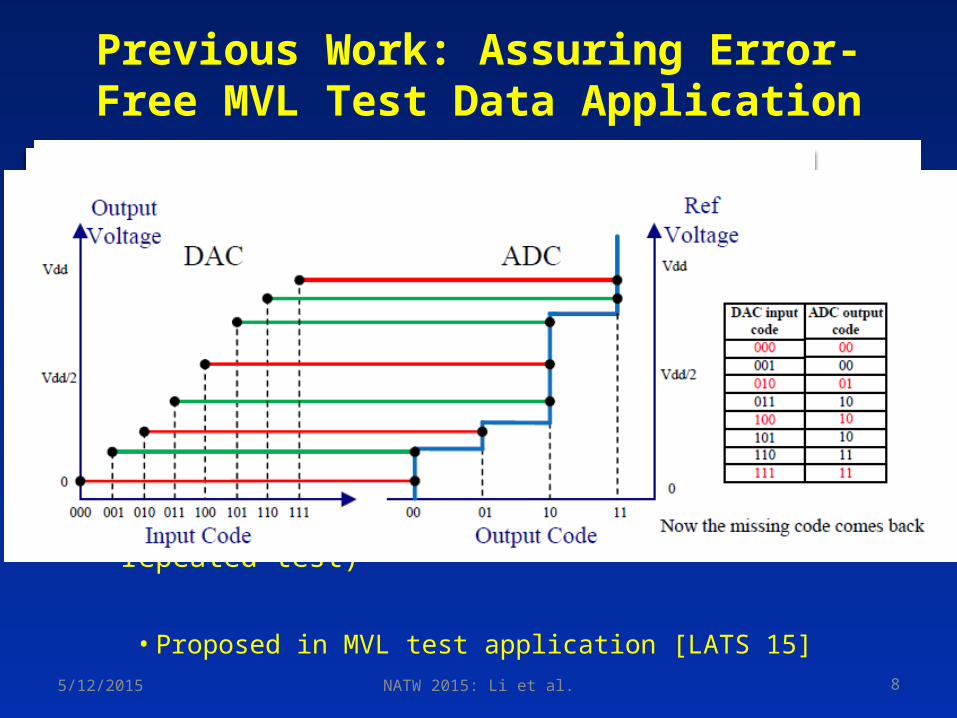
• Two potential error sources for MVL test application– ADC nonlinearities;– Noise effect.
• Solutions– Calibration of ADC nonlinearities (use higher
resolution DAC to generate calibrated MVL signal)– Error detection and test data reapply. (Error
detection circuitry and test flow with repeated test)
• Proposed in MVL test application [LATS 15]
5/12/2015
Previous Work: Assuring Error-Free MVL Test Data Application

NATW 2015: Li et al. 95/12/2015
MVL Test Channel for Reduced Pin-Count SoCs
• How MVL test application resolves test speed sacrifice in RPCT scheme
Scan speed: 1/20 of clock f → 1/5 of clock fSpeed increases by data rate enhancement of MVL channel (log216)
NATW 2015: Li et al. 105/12/2015
A Test Flow
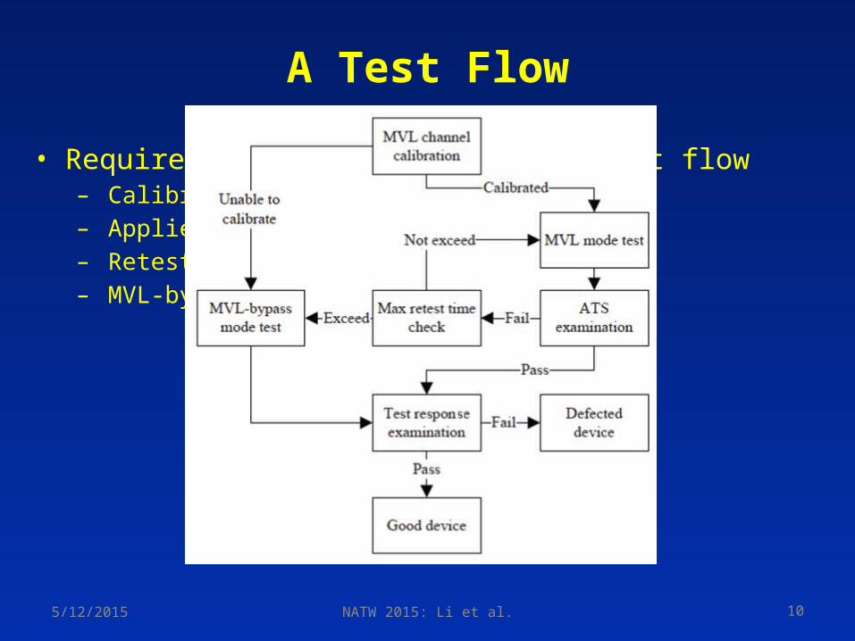
• Requirements on MVL-compatible test flow– Calibration procedure– Applied test data verification– Retest mechanism– MVL-bypass mode test

NATW 2015: Li et al. 11
• RTL diagram
5/12/2015
Hardware Design of 4-bit MVL Channel with 8-bit DAC
Be able to: Generate MVL signal; Run ADC calibration.

NATW 2015: Li et al. 12
• Simulation result of calibration procedure
• Dout is the ramp-up DAC inputs for calibration;• Vre is the captured ADC output, corresponding to Dout;• R1-R14 store the calibrated result.
5/12/2015
Hardware Design of 4-bit MVL Channel with 8-bit DAC

NATW 2015: Li et al. 13
• RTL diagram
5/12/2015
Hardware Design of MVL-Compatible DUT
Mode Test BL Cal Bypass
ADC Nonlinearity Calibration
0 0 1 0
MVL Test 1 1 X 0
ATS Capture 0 0 0 X
Binary Test 1 0 X 1
Be able to: Decode MVL signal; Generate ATS for applied test data verification; Switch between MVL test and MVL-bypass mode.

NATW 2015: Li et al. 14
• Setup of ATE based experiment• Advanrest T2000GS tester builds MVL test channel• An ADC and a DE2 FPGA board build MVL-compatible
DUT with RPCT interface and test decompresser.
• Experiments conducted• Apply scan test with compressed test data through
RPCT interface using MVL signal• Justify the test speed improvement with MVL channel
5/12/2015
Experimental Setup and Results

NATW 2015: Li et al. 155/12/2015
Experimental Setup• Build MVL channel with Advantest
T2000GS

NATW 2015: Li et al. 165/12/2015
Experimental Setup• Build MVL-compatible device with RPCT and
decompresser

NATW 2015: Li et al. 175/12/2015
Experimental Setup• Hardware setup
NATW 2015: Li et al. 18
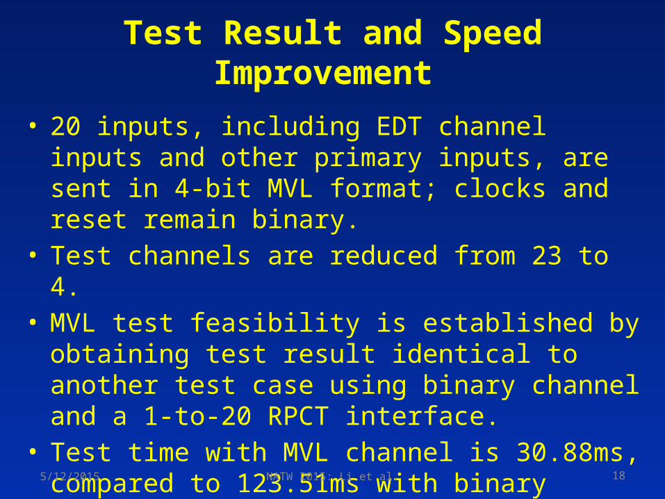
• 20 inputs, including EDT channel inputs and other primary inputs, are sent in 4-bit MVL format; clocks and reset remain binary.
• Test channels are reduced from 23 to 4.• MVL test feasibility is established by
obtaining test result identical to another test case using binary channel and a 1-to-20 RPCT interface.
• Test time with MVL channel is 30.88ms, compared to 123.51ms with binary channel (clock f = 2MHz).
5/12/2015
Test Result and Speed Improvement

NATW 2015: Li et al. 19
• Application of MVL test channel on RPCT with test compression is proposed.
• Reliability issues and proposed solutions are discussed in previous work [LATS 15]; Hardware and a test flow are proposed in this work.
• ATE-based experiments show notable test speed improvement with RPCT.
• Overhead remains an issue but will be helped as data converter techniques evolve.
5/12/2015
Conclusion

NATW 2015: Li et al. 20
• Device with integrated ADC should be tested for feasibility.
• An experiment to validate ADC calibration scheme should be conducted.
• Test flow should be examined with experiments.
5/12/2015
Future Work

NATW 2015: Li et al. 21
• [VTS 11] A. Sanghani et al., “Design and Implementation of A Time-Division Multiplexing Scan Architecture Using Serializer and Deserializer in GPU Chips,” Proc. 29th IEEE VLSI Test Symp., 2011, pp. 219-224.
• [ITC 13] K. Chakravadhanula, et al., “SmartScan - Hierarchical Test Compression for Pin-limited Low Power Designs,” Proc. International Test Conf., 2013. Paper 4.2.
• [ITC 09] J. Moreau et al., “Running scan test on three pins: yes we can!,” Proc. International Test Conf., 2009, pp. 1-10.
• [LATS 15] B. Li et al., Adopting Multi-Valued Logic for Reduced Pin-Count Testing," Proc. 16th Latin-American Test Symposium, 2015.
5/12/2015
Reference