name(xxx) xxx-xxxxemail @canaccord - · pdf filethe oled industry had a cardiac arrest five...
TRANSCRIPT
Canaccord Canaccord Canaccord Canaccord GenuityGenuityGenuityGenuity is the global capital markets group of Canaccord Financial Inc. (CF : TSX | CF. : AIM) is the global capital markets group of Canaccord Financial Inc. (CF : TSX | CF. : AIM) is the global capital markets group of Canaccord Financial Inc. (CF : TSX | CF. : AIM) is the global capital markets group of Canaccord Financial Inc. (CF : TSX | CF. : AIM)
The recommendations and opinions expressed in this Investment Research accurately reflect the Investment Analyst’s personal, The recommendations and opinions expressed in this Investment Research accurately reflect the Investment Analyst’s personal, The recommendations and opinions expressed in this Investment Research accurately reflect the Investment Analyst’s personal, The recommendations and opinions expressed in this Investment Research accurately reflect the Investment Analyst’s personal, independent and independent and independent and independent and objective views about any and all the Designated Investments and Relevant Issuers discussed herein. For important objective views about any and all the Designated Investments and Relevant Issuers discussed herein. For important objective views about any and all the Designated Investments and Relevant Issuers discussed herein. For important objective views about any and all the Designated Investments and Relevant Issuers discussed herein. For important information, please see the Important Disclosures section in the appendix of this document or visit Canaccord Genuity’s information, please see the Important Disclosures section in the appendix of this document or visit Canaccord Genuity’s information, please see the Important Disclosures section in the appendix of this document or visit Canaccord Genuity’s information, please see the Important Disclosures section in the appendix of this document or visit Canaccord Genuity’s Online Disclosure Online Disclosure Online Disclosure Online Disclosure DatabaseDatabaseDatabaseDatabase.... 11114444 NNNNoooovvvveeeemmmmbbbbeeeerrrr 2222000011111111 2222000011111111----111122221111
Jonathan DorsheimerJonathan DorsheimerJonathan DorsheimerJonathan Dorsheimer
1.617.371.3875 [email protected]
Josh Baribeau, CFAJosh Baribeau, CFAJosh Baribeau, CFAJosh Baribeau, CFA
1.617.371.3892 [email protected]
Inside Executive summary 2 OLED market size 3 Suppliers 17 History 22 Lighting industry 24 Technology 29 Manufacturing 36 Physics 50 Performance 53 Multi-touch technology 57
Sustainability & CleanTech -- Energy & Power Technologies
OLEDs 101OLEDs 101OLEDs 101OLEDs 101 The 20-year overnight sensation
• We are introducing the Canaccord Genuity Organic Light Emitting Diode (OLED) global supply and demand model plus forecasts through 2020. We present our analysis in the same three-case scenario that we have adopted in our other areas of focus.
• We forecast that AMOLED small/medium display sales by 2020 will reach from $8.9B to $22.4B, with large area sales reaching from $8.1B to $15.0B. We expect lighting to remain a niche market with sales of between $216M and $401M.
• We are currently tracking the capacity and capex plans of 11 manufacturers and 29 separate fabs currently online or expected to come online in the next five years. We predict capex over this time frame to be in excess of $5B for the backplane array and the OLED processes.
• These facilities should bring worldwide manufacturing capacity to approximately 11.1M square meters annually by 2015, led by Samsung with almost 6M square meters of this total.
• We anticipate total OLED materials revenues to range from a $321M to $597M annual market by 2015, depending on market adoption and capacity growth, up from around $96M in 2010.
• It has yet to be determined which of the transistor backplane technologies will emerge as the dominant technology. Many exist, each offering their individual merits, but manufacturers are currently working through yield and/or scale issues for them all.
2
OLEDs 101 14 November 2011
EXECUTIVE SUMMARY We have tracked the OLED industry for the better part of a decade, and for most of this time we have listened to hundreds of predictions about how OLEDs would render LCD, plasma and other display technologies obsolete. In fact, as our title to this report implies, pundits have been predicting “hockey stick” growth for years. So what eluded everyone, and why now? Will this be yet another false start?
In this report, we are attempting to provide context of the market by defining how we think the OLED industry will ramp through our Base case scenario, but we also outline a set of assumptions that could create upside in our Bullish scenario and downside in our Bearish scenario. We worked extensively with Barry Young of the OLED Association, Samsung Mobile, LG Display and many others to gain greater clarity into this technology and ramp.
Unlike their inorganic cousins, OLEDs are stacks of organic materials bonded together by carbon and hydrogen. When electrically excited, an atom’s state is changed and an exciton is created – light. What makes OLEDs truly compelling is the ability to simplify the complexity of a display compared to an LCD – the most widely used display technology today – and thus reduce costs.
Cheaper, thinner, better? The value proposition for OLEDs is simple: reduce costs by capturing more light produced (removing color filters), improve picture quality as the technology is emissive versus transmissive, while passing the WAF factor (wife approval factor) with a sexier form…thin is in. Sound promising? So why are OLEDs less than 1% of the display and lighting industry currently?
The OLED industry had a cardiac arrest five years ago, when almost every OEM shelved or reduced R&D dollars associated with OLEDs. The only exception was Samsung SDI, later Samsung Mobile Device (SMD), a JV between Samsung Electronics and SDI. It is our opinion that SMD, with a defibrillator in hand, resuscitated the OLED industry by commercializing active matrix OLEDs for the mobile market last year.
From an application perspective there are many challenges associated with OLEDs that are perhaps the reason it has taken so long for the technology to be commercialized. OLEDs are in fact less efficient than LCDs at the moment in smartphone applications. This has to do with application usage. If the user is watching full video, OLEDs offer greater battery life; however, few people watch extensive video on their handsets. The greatest usage is web browsing. Recreating the white background that most web pages have requires a great deal of power, which drains the battery, not to mention reducing the display’s lifetime.
For TV applications, other considerations are critical. While picture quality is arguably better, scaling costs to Gen8 manufacturing facilities is not clear, largely due to the transistor backplane materials (a-Si, LTPS, Metal oxide TFT). Lifetimes are also an issue – 50K hours are required for TVs vs. only 5K for handsets.
Despite the technical limitations, SMD expects to spend over $10B in CAPEX between 2010 and 2013. Handset OEMs find the ability to differentiate through the display compelling, and costs are becoming more competitive. As a result, we believe OLEDs hold tremendous growth potential, which we outline throughout this report. As is our standard practice, we will consider this document living and plan to update it at least twice per year, with this version being 1.0.

3
14 November 2011 OLEDs 101
OLED MARKET SIZE As usual we will present our three-scenario analysis for the OLED market’s size. We begin with Canaccord Genuity’s global handset, tablet, TV and lighting forecasts and then make assumptions for the OLED penetration therein. We also back check our numbers against third-party forecasts, more heavily weighted toward those of Young Market Research (YMR) and the OLED Association. Generally those forecasts tend to correlate with our Bull case scenario.
OLED production forecast The OLED market can be divided into four segments, 1) small/medium active matrix OLEDs (AMOLEDs) for handsets and tablets, 2) Large Area Displays, primarily for TVs, using AMOLEDs; 3) Solid State Lighting using passive matrix OLEDs (PMOLEDs); and 4) small/medium displays using PMOLEDs. Each of these categories is in very different stages of development. PMOLEDs for small/medium displays are very mature and have entered a period of negative growth; AMOLEDs for small/medium displays have been around for some time but are still less mature and growing rapidly. AMOLED TVs are in the R&D stage – some TVs built on pilot lines have demonstrated the performance benefits of AMOLEDs, but not the cost effectiveness. OLED lighting is in an immature state: some lighting products are in production but are being sold at very high prices.
We forecast the total market size for OLED devices to range from $17.2B to $37.7B by 2020 from a base of US$1.4B in 2010. Note that these estimates and all market size estimates in this report are for the display module, which we feel is a better proxy in calculating the OLED market opportunity, and do not include the cost of embedded touch, which currently adds between $5-$10 per display.
Revenue – Displays and Lighting OLED device revenue in 2010 was $1.4B, and we expect it to grow to approximately $2.5B in 2011. The bulk of the revenue today comes from Small/Medium displays as TVs and lighting are basically nil. By 2020, however, we forecast that AMOLED small/medium sales will reach from $8.9B - $22.4B, with large area sales to reach from $8.1B - $15.0B. We expect lighting to remain a niche market with sales of between $216M and $401M.

4
OLEDs 101 14 November 2011
Figure 1: OLED device revenue
Base
0
5,000
10,000
15,000
20,000
25,000
30,000
35,000
2011
2012
2013
2014
2015
2016
2017
2018
2019
2020
Reven
ue ($M)
Lighting
TV
Tablet
Handset
Bear
0
2,000
4,000
6,000
8,000
10,000
12,000
14,000
16,000
18,000
20,000
2011
2012
2013
2014
2015
2016
2017
2018
2019
2020
Reven
ue ($M)
Lighting
TV
Tablet
Handset
Bull
0
5,000
10,000
15,000
20,000
25,000
30,000
35,000
40,000
2011
2012
2013
2014
2015
2016
2017
2018
2019
2020
Reven
ue ($M)
Lighting
TV
Tablet
Handset
Source: Canaccord Genuity
The primary application driving AMOLED production is the smartphone, because of growing requirements for high contrast, thin form factor, wide viewing angle and soon to be very high pixel density. Apple has been driving this market, but the Samsung’s Galaxy line using the Android operating system and AMOLED display is making significant headway against the iPhone. Although Apple has not used AMOLEDs so far, it is possible that after 2012, when AMOLEDs achieve a similar pixel density and lower power consumption, Apple could switch from LCD – assuming there is sufficient capacity to meet Apple’s needs. Other S/M applications such as digital cameras, near-eye displays, portable media players, etc. have already begun to adopt OLED displays; however these displays tend to be rather small relative to handsets and are much smaller in volume, so do not weigh heavily on our forecasts.
TVs are another long-term opportunity as the media and consumer generally agree that the demonstration-type AMOLED TVs offer a viewing experience unmatched by any of the existing technologies. The problem for AMOLEDs has been the capability to scale the

5
14 November 2011 OLEDs 101
manufacturing process, but a number of breakthroughs over the past year seem to indicate that a solution will be operational by 2013. Despite the promise, we continue to expect the dominant application for OLEDs will be the mobile market. The forecasts above show the majority of display revenues in the AMOLED space will be dominated by mobile phones, followed by TVs. While the TV market may prove to be more or less a niche market, the relative size and value difference between a TV display and mobile display skew the relative figures.
Shipments -- Displays and Lighting We predict that overall shipment volumes in 2011 will range from 55M to 90M units, growing to a range of 471M to 998M units by 2020. As shown in Figure 2, S/M AMOLEDs are carrying the bulk of the growth as TVs and Lighting contribute very little to the volume initially. It is forecasted that the TVs will begin volume production in 2013 with the introduction of 8th Gen fabs by LG Display and Samsung (SMD). OLED Lighting should begin shipping in commercial volumes in 2012 as both Osram and Philips are building new fabs, but is likely to remain small as a percentage of the total.

6
OLEDs 101 14 November 2011
Figure 2: OLED device shipment estimates
Base
0
100
200
300
400
500
600
700
800
900
2011
2012
2013
2014
2015
2016
2017
2018
2019
2020
Shipmen
ts (M)
Lighting
TV
Tablet
Handset
Bear
0
50
100
150
200
250
300
350
400
450
500
2011
2012
2013
2014
2015
2016
2017
2018
2019
2020
Shipmen
ts (M)
Lighting
TV
Tablet
Handset
Bull
0
200
400
600
800
1000
1200
2011
2012
2013
2014
2015
2016
2017
2018
2019
2020
Shipmen
ts (M)
Lighting
TV
Tablet
Handset
Source: Canaccord Genuity
AMOLED small/medium volumes are projected to be between 428M and 919M units by 2020, primarily displays for smart phones, out of a TAM we peg at 960M smart phones plus 232M tablets. We believe penetration rates for handsets could range from 39% to as high as 72% with tablet penetration of between 25% and 100%, largely dependent on Apple’s plans. TVs are projected to reach from 40M and 74M units 40” and greater out of a TAM of >280M TVs, or penetration of 14% to 26%. By 2020, we see OLED lighting at around 3.4M to 6.2M units (largely 6” square panels); a negligible percentage of the total lighting market.

7
14 November 2011 OLEDs 101
Figure 3: OLED shipment estimates (handset)
Handsets
0
100
200
300
400
500
600
700
800
2011
2012
2013
2014
2015
2016
2017
2018
2019
2020
Shipmen
ts (M)
0%
10%
20%
30%
40%
50%
60%
70%
80%
Bear
Base
Bull
Penetration Bear
Penetration Base
Penetration Bull
Source: Canaccord Genuity Figure 4: OLED shipment estimates (tablet)
Tablets
0
50
100
150
200
250
2011
2012
2013
2014
2015
2016
2017
2018
2019
2020
Shipmen
ts (M)
0%
10%
20%
30%
40%
50%
60%
70%
80%
90%
100%
Bear
Base
Bull
Penetration Bear
Penetration Base
Penetration Bull
Source: Canaccord Genuity

8
OLEDs 101 14 November 2011
Figure 5: OLED shipment estimates (TV)
TVs
0
10
20
30
40
50
60
70
80
2011
2012
2013
2014
2015
2016
2017
2018
2019
2020
Shipmen
ts (M)
0%
10%
20%
30%
40%
50%
60%
70%
80%
90%
100%
Bear
Base
Bull
Penetration Bear
Penetration Base
Penetration Bull
Source: Canaccord Genuity
OLED capex Over the period from 2011 to 2015, we project that 21 AMOLED fabs will be in operation. We divide the capex therein into two parts: 1) OLED processing, including the deposition, patterning and encapsulation processes; and 2) transistor array backplane (active matrix), including the deposition, lithography, and crystallization processes. Our capex estimates are based only on equipment and do not include the facility, building or the module process, which would add 30% to 40% to the total.
Over the four-year time frame, we expect OLED capex to be over $5B for the OLED array and the OLED processes. Note we consider capex as of the expected equipment order date, which currently is 12 to 18 months before the tools go into production. Samsung Mobile Displays (SMD) is the clear leader with over half of the expected capex industry-wide.
Samsung's 2011 planned capex for AMOLED processes, module and facility is KRW5.4T ($5B), which happens to be larger than that in traditional LCD (KRW4.1T), with reports of KRW7.0T for OLED in 2012. It is also worth noting that part of the LCD capex could be transferred to AMOLED-related capex if the LCD TV demand stays sluggish. Parts of the fab such as the LCD clean rooms can be switched over to the AMOLED production line, for example.
LG Display (LGD) has decided to skip Gen 5.5 and go straight to Gen 8 with AMOLED investments already begun and a goal to have a commercial TV by the end of 2012/early 2013. Several Japanese display and TV makers are working on AMOLED technology but it is not a mainstream product for any of them, and their commitment of resources is a small fraction of Samsung’s or LG’s. Sony, for example, is working on OLED product development, but OLED is only one of the next-generation display technologies it is

9
14 November 2011 OLEDs 101
exploring. AUO and CMI expect to have Gen 3 fabs operating in late 2011. Several Chinese panel makers are also planning to have AMOLED fabs by 2012 or 2013.
Figure 6: Process capex by panel maker, 2011-2015E ($M)
OLED Array TotalSMD 1084.0 1746.2 2830.2LGD 349.0 513.4 862.3AUO 238.7 390.3 628.9CMI 103.2 190.4 293.5
Visionox 75.4 177.9 253.2PAN 44.4 94.4 138.8BOE 44.4 94.4 138.8
IRICO 37.7 88.9 126.6Total 1976.6 3295.9 5272.5
Source: YMR
Figure 7: Forecasted capex for OLED processing
0.0
200.0
400.0
600.0
800.0
1000.0
1200.0
2011 2012 2013 2014
US$
(m)
IRICO
BOE
PAN
Visionox
CMI
AUO
LGD
SMD
Source: YMR
The capex forecast for the array process is based on the assumption that the small fabs, except for one (AUO Gen 4.5), are brand new and will use low temperature polysilicon (LTPS) technology, described below. It is highly likely that the larger fabs, Gen 6 and above, will already be in existence, having been converted from preexisting and depreciated LCD factories. We therefore expect that these fabs will not require the full investment in array tools, although these larger LCD fabs use an amorphous silicon (a-Si) array technology that is unsuitable for OLED displays and will require further investment.

10
OLEDs 101 14 November 2011
There are three possible OLED array technologies, which we describe in more detail below, but for now we will assume all of the fabs will be additive to capacity and will use LTPS. Should these amorphous silicon fabs use one of the other array technologies, our estimates would be subject to change. We predict the greatest investment in the next few years to occur in 2012.
Figure 8: Forecasted capex for array processing
0.0
200.0
400.0
600.0
800.0
1000.0
1200.0
1400.0
1600.0
1800.0
2011 2012 2013 2014
US$
(m)
IRICO
BOE
PAN
Visionox
CMI
AUO
LGD
SMD
Source: YMR
The most significant measure of production volume in the display industry is the mother glass size and capacity/month. Figure 9 shows the manufacturer, substrate size and mother glass capacity for the AMOLED manufacturers from 2009 to 2015E. The table shows two substrate sizes for each installation because in some cases the manufacturers have chosen to use one size for the active matrix and another size for the OLED process. For example, Samsung chose one Gen 4.5 (730mmx920mm) process to deposit and create the array and it then cuts the glass into two Gen 3.5 sized substrates (730mmx460mm) for the OLED process. For their Gen 5.5 (1300mmx1500mm) array fab, the mother glass is cut into four G3.5-sized pieces for the OLED process.

11
14 November 2011 OLEDs 101
Figure 9: AMOLED fab capacity by substrate size and OLED substrates/year
Status Manufacturer Location Generation Size Generation Size 2009 2010 2011 2012 2013 2014 2015R&D LGD Kumi 2 370x470 2 370x470 48 48 48 48 48 48 48Pilot LGD Kumi 4.5 730x920 3.5 730x460 36 72 72 72 72 72 72
Production LGD Kumi 4.5 730x920 3.5 730x460 0 0 108 336 336 336 336Production LGD Kumi 8 2200x2500 7 2000x1250 0 0 3 66 240 480 768Production SMD Chenon 4.5 730x920 3.5 730x460 960 1152 1344 1344 1344 1344 1344Production SMD Tangjeong 5.5 1300x1500 4 650x750 0 0 336 2304 3456 3456 3456Production SMD Tangjeong 5.5 1300x1500 5.5 1300x1500 0 0 0 0 168 168 168Production SMD Tangjeong 5.5 1300x1500 5.5 1300x1500 0 0 0 0 42 168 168Production SMD Tangjeong 8 2200x2520 4.5 1100x840 0 0 3 78 216 432 864
Pilot SMD 8 2200x2520 8 2200x2520 0 0 0 0 210 360 360R&D AUO Hsinchu 1 200x200 1 200x200 12 12 12 12 12 12 12Pilot AUO Hsinchu 3.25 620x750 4 620x750 0 0 6 12 12 12 12
Production AUO Hinschu 3.25 620x750 4 620x750 0 0 12 138 144 180 180Production AUO Hinschu 6 1500x1800 6 1500x1800 0 0 0 0 0 198 360Production AUO Singapore 4.5 730X920 3.5 730X460 0 0 0 45 312 1080 1080Production CMI Hsinchu, Taiwan 3.5 620x750 3.25 620x375 117 168 168 168 168 168 168Production PAN 6 1500x1800 6 1500x1800 0 0 0 0 192 360 504R&D CMI Tainan,Taiwan 1 200x200 1 200x200 12 12 12 12 12 12 12
Production CMI Hsinchu, Taiwan 3.5 1300x1500 3.5 650x750 0 0 0 0 360 960 960Production CMI Hsinchu, Taiwan 2 370x470 2 370x470 12 12 12 12 12 12 12Production Sony Higashiura, Japan 3.5 600x720 3.5 600x720 36 36 36 36 36 36 36Production Visionox Beijing, China 4 730x920 3.5 730x460 0 0 0 0 120 144 288Production IRICO Foshas, China 4 730x920 3.5 730x460 0 0 0 0 144 144 144
Pilot Tianma Shanghai, China 2 370x470 2 370x470 0 0 0 90 144 144 144Production Tianma Shanghai, China 4.5 730x920 3.5 730x460 0 0 0 6 48 48 48Production Tianma Xianmen 5.5 1320x1500 5.5 1320x1500 0 0 0 0 6 12 12R&D BOE Chengdu, China 2 370x470 2 370x470 0 0 0 0 36 180 432R&D Ortus Kochi1 1 200x200 1 200x200 12 12 12 12 12 12 12Pilot Ortus Saitama 1 2 370x470 2 370x470 0 0 3 36 57 60 60
TFT OLED Substrates / year
Source: YMR
Figure 9: AMOLED fab capacity by substrate size and OLED substrates/year
Figure 10 shows capacity in terms of area from 2009 to 2015E. We predict that there will be approximately 11.1M square meters of annual OLED capacity by 2015, led by Samsung and LG.
Figure 10: Capacity estimates by manufacturer
0
2,000
4,000
6,000
8,000
10,000
12,000
2009
2010
2011
2012
2013
2014
2015
Area (m
2, 000
s)
China
Sony
Panasonic
CMI
AUO
LG
Samsung
Source: Canaccord Genuity

12
OLEDs 101 14 November 2011
OLED material (by kg)
As we will describe below, OLED devices use a variety of chemicals between their various layers, called a “stack.” We forecast total OLED material usage to increase to between 1,106kg and 2,055kg by 2020, from an estimated 250kg for 2011. In looking at the numbers, it is important to notice that volumes do not scale linearly with capacity. As companies come up the learning curve we assume material utilization will become more effective, reducing the amount wasted per run.
Each display uses a minute amount of each material, but the materials are highly engineered and very expensive. The chemicals range from approximately $200 per gram to upwards of $3,000 per gram. Thickness of the deposited films range from 0.5 nanometers to 46 nanometers, depending on the layer. We do not project significant commoditization or rapid declines in the materials’ pricing due to their highly complex nature, patent protection in some cases and relatively small overall usage. Below are our materials utilization assumptions – the low numbers indicate that much of each material is wasted. For example, 93% of the dopant materials are wasted in the manufacturing process currently (for reasons described in the manufacturing section below). While waste is expected to decline gradually, we do not expect order-of-magnitude-type advancements in the coming years.
Figure 11: Chemical utilization estimates
2009 2010 2011 2012 2013 2014 2015HIL 30% 35% 40% 45% 50% 55% 60%HTL 30% 35% 40% 45% 50% 55% 60%HB 30% 35% 40% 45% 50% 55% 60%B HOST 3% 5% 7% 9% 11% 13% 15%B Dopant 3% 5% 7% 9% 11% 13% 15%ETL 30% 35% 40% 45% 50% 55% 60%R Host 3% 5% 7% 9% 11% 13% 15%R Dopant 3% 5% 7% 9% 11% 13% 15%G HOST 3% 5% 7% 9% 11% 13% 15%G Dopant 3% 5% 7% 9% 11% 13% 15%
Materials Utilization
Source: Canaccord Genuity
We anticipate total chemicals revenues to range from a $96M annual market today to a $321M-597M annual market by 2015, depending on market adoption and capacity growth.

13
14 November 2011 OLEDs 101
Figure 12: Chemical revenue estimates
2009 2010 2011 2012 2013 2014 2015HIL 365,123 1,029,218 1,331,400 1,714,459 3,357,322 5,777,797 8,367,015 HTL 2,464,577 6,947,218 8,986,950 11,572,596 22,661,921 39,000,131 56,477,354 HB 182,561 514,609 665,700 857,229 1,678,661 2,888,899 4,183,508 B HOST 2,135,967 4,214,646 4,450,680 5,014,792 8,927,424 14,300,048 19,578,816 B Dopant 3,012,261 5,943,731 6,276,600 7,072,142 12,589,956 20,166,734 27,611,151 ETL 1,469,618 4,142,601 5,358,885 6,900,696 13,513,220 23,255,633 33,677,237 R Host 6,937,328 13,688,593 14,455,200 16,287,357 28,995,051 46,444,600 63,589,317 R Dopant 2,738,419 5,403,392 6,240,938 6,155,636 11,043,821 17,270,589 23,830,107 G HOST 4,162,397 8,213,156 8,673,120 9,772,414 17,397,030 27,866,760 38,153,590 G Dopant 5,257,764 10,374,513 10,955,520 11,818,821 21,204,137 33,159,531 45,753,806
28,726,013$ 60,471,676$ 67,394,993$ 77,166,143$ 141,368,542$ 230,130,722$ 321,221,903$
Materials Sales, Bear
2009 2010 2011 2012 2013 2014 2015HIL 365,123 1,029,218 1,902,000 2,449,227 4,796,174 8,253,996 11,952,879 HTL 2,464,577 6,947,218 12,838,500 16,532,280 32,374,173 55,714,472 80,681,935 HB 182,561 514,609 951,000 1,224,613 2,398,087 4,126,998 5,976,440 B HOST 2,135,967 4,214,646 6,358,114 7,163,988 12,753,462 20,428,640 27,969,737 B Dopant 3,012,261 5,943,731 8,966,571 10,103,060 17,985,652 28,809,620 39,444,501 ETL 1,469,618 4,142,601 7,655,550 9,858,137 19,304,600 33,222,333 48,110,339 R Host 6,937,328 13,688,593 20,650,286 23,267,653 41,421,501 66,349,429 90,841,882 R Dopant 2,738,419 5,403,392 8,915,625 8,793,766 15,776,888 24,672,270 34,043,010 G HOST 4,162,397 8,213,156 12,390,171 13,960,592 24,852,901 39,809,657 54,505,129 G Dopant 5,257,764 10,374,513 15,650,743 16,884,031 30,291,624 47,370,759 65,362,580
28,726,013$ 60,471,676$ 96,278,561$ 110,237,347$ 201,955,060$ 328,758,175$ 458,888,433$
Materials Sales, Base
2009 2010 2011 2012 2013 2014 2015HIL 365,123 1,029,218 2,472,600 3,183,995 6,235,026 10,730,195 15,538,743 HTL 2,464,577 6,947,218 16,690,050 21,491,964 42,086,425 72,428,814 104,886,515 HB 182,561 514,609 1,236,300 1,591,997 3,117,513 5,365,097 7,769,371 B HOST 2,135,967 4,214,646 8,265,549 9,313,184 16,579,501 26,557,232 36,360,659 B Dopant 3,012,261 5,943,731 11,656,543 13,133,978 23,381,347 37,452,506 51,277,852 ETL 1,469,618 4,142,601 9,952,215 12,815,579 25,095,979 43,189,033 62,543,441 R Host 6,937,328 13,688,593 26,845,371 30,247,949 53,847,951 86,254,257 118,094,447 R Dopant 2,738,419 5,403,392 11,590,313 11,431,896 20,509,954 32,073,951 44,255,914 G HOST 4,162,397 8,213,156 16,107,223 18,148,770 32,308,771 51,752,554 70,856,668 G Dopant 5,257,764 10,374,513 20,345,966 21,949,240 39,379,111 61,581,987 84,971,354
28,726,013$ 60,471,676$ 125,162,129$ 143,308,551$ 262,541,579$ 427,385,627$ 596,554,963$
Materials Sales, Bull
Source: Canaccord Genuity
Perhaps the most relevant metric in the materials space is the phosphorescent dopant revenue potential, as it is viewed as the key material and that which actually emits the light; and sold by the only public pure-play company in the space, Universal Display Corp. Below is a consolidated graphic of both the red emitter and green emitter forecasts shown in the table above. We have not broken out the blue materials because blue phosphorescent emitter materials are currently not competitive commercially. The decline in dollar values of some materials from 2010 to 2009 is largely a result of production shifting from development volumes to commercial agreements and better materials utilization/less waste. We project that cumulative red emitter revenues will total between $64.5M and $119.9M between 2011 and 2015 with cumulative green emitter revenues of between $122.9M and $228.2M in the same time period.

14
OLEDs 101 14 November 2011
Figure 13: Emitter sales estimates
Red Dopant Sales
$0.0
$5.0
$10.0
$15.0
$20.0
$25.0
$30.0
$35.0
$40.0
$45.0
$50.0
2009
2010
2011
2012
2013
2014
2015
Millions
Bear
Base
Bull
Green Dopant Sales
$0.0
$10.0
$20.0
$30.0
$40.0
$50.0
$60.0
$70.0
$80.0
$90.0
2009
2010
2011
2012
2013
2014
2015
Millions
Bear
Base
Bull
Source: Canaccord Genuity
PMOLED
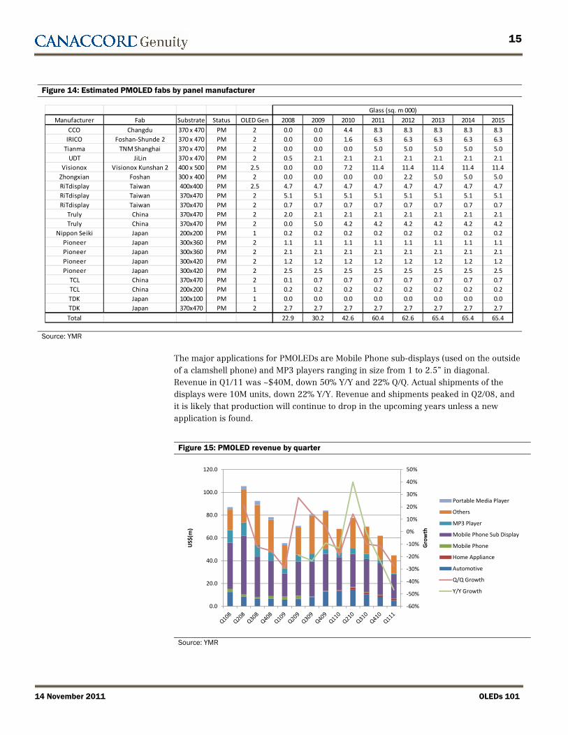
Currently, there are 12 companies making PMOLEDs, the capacity of which are detailed in Figure 14. All of the fabs are in the Gen 1 to Gen 2.5 class. Despite being limited by size and resolution, the industry started with PMOLEDs due to the lower investment requirements and technical hurdles. A 2nd Gen facility costs on the order of $50M, an order of magnitude less than what it would take to build an active matrix line of the same size.
15
14 November 2011 OLEDs 101
Figure 14: Estimated PMOLED fabs by panel manufacturer
Manufacturer Fab Substrate Status OLED Gen 2008 2009 2010 2011 2012 2013 2014 2015
CCO Changdu 370 x 470 PM 2 0.0 0.0 4.4 8.3 8.3 8.3 8.3 8.3IRICO Foshan-Shunde 2 370 x 470 PM 2 0.0 0.0 1.6 6.3 6.3 6.3 6.3 6.3
Tianma TNM Shanghai 370 x 470 PM 2 0.0 0.0 0.0 5.0 5.0 5.0 5.0 5.0UDT JiLin 370 x 470 PM 2 0.5 2.1 2.1 2.1 2.1 2.1 2.1 2.1
Visionox Visionox Kunshan 2 400 x 500 PM 2.5 0.0 0.0 7.2 11.4 11.4 11.4 11.4 11.4Zhongxian Foshan 300 x 400 PM 2 0.0 0.0 0.0 0.0 2.2 5.0 5.0 5.0RiTdisplay Taiwan 400x400 PM 2.5 4.7 4.7 4.7 4.7 4.7 4.7 4.7 4.7RiTdisplay Taiwan 370x470 PM 2 5.1 5.1 5.1 5.1 5.1 5.1 5.1 5.1RiTdisplay Taiwan 370x470 PM 2 0.7 0.7 0.7 0.7 0.7 0.7 0.7 0.7
Truly China 370x470 PM 2 2.0 2.1 2.1 2.1 2.1 2.1 2.1 2.1Truly China 370x470 PM 2 0.0 5.0 4.2 4.2 4.2 4.2 4.2 4.2
Nippon Seiki Japan 200x200 PM 1 0.2 0.2 0.2 0.2 0.2 0.2 0.2 0.2Pioneer Japan 300x360 PM 2 1.1 1.1 1.1 1.1 1.1 1.1 1.1 1.1Pioneer Japan 300x360 PM 2 2.1 2.1 2.1 2.1 2.1 2.1 2.1 2.1Pioneer Japan 300x420 PM 2 1.2 1.2 1.2 1.2 1.2 1.2 1.2 1.2Pioneer Japan 300x420 PM 2 2.5 2.5 2.5 2.5 2.5 2.5 2.5 2.5
TCL China 370x470 PM 2 0.1 0.7 0.7 0.7 0.7 0.7 0.7 0.7TCL China 200x200 PM 1 0.2 0.2 0.2 0.2 0.2 0.2 0.2 0.2TDK Japan 100x100 PM 1 0.0 0.0 0.0 0.0 0.0 0.0 0.0 0.0TDK Japan 370x470 PM 2 2.7 2.7 2.7 2.7 2.7 2.7 2.7 2.7Total 22.9 30.2 42.6 60.4 62.6 65.4 65.4 65.4
Glass (sq. m 000)
Source: YMR
The major applications for PMOLEDs are Mobile Phone sub-displays (used on the outside of a clamshell phone) and MP3 players ranging in size from 1 to 2.5” in diagonal. Revenue in Q1/11 was ~$40M, down 50% Y/Y and 22% Q/Q. Actual shipments of the displays were 10M units, down 22% Y/Y. Revenue and shipments peaked in Q2/08, and it is likely that production will continue to drop in the upcoming years unless a new application is found.
Figure 15: PMOLED revenue by quarter
-60%
-50%
-40%
-30%
-20%
-10%
0%
10%
20%
30%
40%
50%
0.0
20.0
40.0
60.0
80.0
100.0
120.0
Gro
wth
US$
(m)
Portable Media Player
Others
MP3 Player
Mobile Phone Sub Display
Mobile Phone
Home Appliance
Automotive
Q/Q Growth
Y/Y Growth
Source: YMR

16
OLEDs 101 14 November 2011
Figure 16: PMOLED shipment volume by quarter
-40%
-30%
-20%
-10%
0%
10%
20%
30%
40%
50%
60%
0
5,000
10,000
15,000
20,000
25,000
Gro
wth
Ship
men
ts (0
00)
Portable Media Player
Others
MP3 Player
Mobile Phone Sub Display
Mobile Phone
Home Appliance
Automotive
Q/Q Growth
Y/Y Growth
Source: YMR
Figure 17: PMOLED annual revenue forecast by application
-25%
-20%
-15%
-10%
-5%
0%
5%
10%
$0.0
$50.0
$100.0
$150.0
$200.0
$250.0
$300.0
$350.0
$400.0
Gro
wth
US$
m
Portable Media Player
Others
MP3 Player
Mobile Phone Sub Display
Mobile Phone
Home Appliance
Automotive
Portable Media Player
Source: YMR

17
14 November 2011 OLEDs 101
Figure 18: PMOLED annual shipment forecast by application
-25%
-20%
-15%
-10%
-5%
0%
5%
10%
15%
0
10,000
20,000
30,000
40,000
50,000
60,000
70,000
80,000
90,000
2008 2009 2010 2011 2012 2013 2014 2015 2016 2017
Ship
men
ts (0
00)
Portable Media Player
Others
MP3 Player
Mobile Phone Sub Display
Mobile Phone
Home Appliance
Automotive
Y/Y Growth
Source: YMR
Given the continued drop in PMOLED demand and the relative stability of supply, the PMOLED display makers are looking at alternatives for using the fully depreciated capacity. The uses that are being examined include:
• Using the fabs to produce OLED lighting. Pioneer is already cooperating with Mitsubishi to make lighting panels, which are similar to PMOLEDs from a driving and backplane perspective.
• Utilizing merchant a-Si backplanes to make AMOLEDs. RiTdisplay announced that they would have a 3.5” product available by the end of 2011. They are using technology licensed from IGNIS Innovation, which has invented a way to compensate for the reliability issues of a-Si. RiTdisplay is purchasing backplanes from a Taiwanese manufacturer.
• Utilizing an active addressing driving scheme to extend the number of rows that can be addressed productively. The scheme involves analyzing the color level of all subpixels and calculating a method to reduce the time it takes to drive all the rows by addressing multiple rows at a time. Such a scheme has been developed by Dialog Semiconductor and is being used by TDK.
SUPPLIERS
Korea
As indicated previously, OLED display production is dominated by Samsung Mobile Display (SMD – a JV between Samsung Electronics and Samsung SDI). SMD is building its own supply chain, essentially forcing LGD to do the same. SMD has become obsessed with keeping the technology in-house and is forbidding its suppliers to do business with other panel makers by making exclusive contracts for products that were co-developed

18
OLEDs 101 14 November 2011
with Samsung. Early on in the development of OLED displays, most of the key equipment was supplied by the Japanese and exclusivity was not possible. However, as the market expanded and the demand for larger and more efficient tools grew, most of the equipment had to be specially developed, forcing Samsung to subsidize tool makers and material suppliers. SMD preferred to use Korean suppliers to protect against technology and intellectual property leakage. LGD had to either develop its own suppliers or wait for Japanese equipment makers to come up with 8G AMOLED fab equipment. SMD was more limited in terms of material, but still controls the source for hole transport and extraction layers.
SMD had to rely on Japanese suppliers for their Gen 4.5 fab (Tokki, acquired by Canon of Japan; Japan Steel Works (JSW); Daifuku; etc.) for the key evaporation and encapsulation equipment. At the time the evaporation equipment could handle only small-sized panels (one-half of the 4.5G size). For the Gen5.5 and larger, SMD is working with many Korean companies. AP Systems was the first Korean company that began supplying ELA (excimer laser annealing) tool and glass encapsulation tools for SMD’s 5.5G fab. AP systems is not the sole supplier in the market, as both SNU Precision and SFA are developing encapsulation tools.
Korean companies SNU and SFA and Japanese makers Tokki and ULVAC are competing in the evaporation tool segment. Vacuum logistics and the automation system are likely to change from Daifuku to SFA. When it comes to organic material suppliers, most of the key suppliers are Korean companies. Except for the red, green and blue dopant layers, most of the other organic materials in the OLED stack are from domestic companies: Duksan Hi-Metal (DS Hi-Metal), LG Chemical, Doosan Electronics, Sun Fine Chemicals and Gracell (acquired by Dow Chemical).
Figure 19: SMD equipment suppliers by fab
Equipment 4.5 G Suppliers
Phase 1 and 2 5.5 G Suppliers
Phase3 5 G Suppliers
8 G Suppliers
Laser Crystallization JSW AP Systems AP Systems/TCZ AP Systems/ TCZ
Evaporation/Printing Tokki Tokki SFASNU, SFA,AP Systems, DNS
LITI N-Light N-Light
Encapsulation TokkiAP Systems, SNU Precision
AP Systems, SNU Precision
AP Systems, SNU Precision
Vacuum Logistics Daifuku Daifuku, SFA Daifuku, SFA Daifuku, SFA
Source: YMR
SMD has made it clear that it intends to use Korean material suppliers whenever possible, and these arrangements are expected to be exclusive. Such exclusive arrangements are advantageous to the material suppliers currently as SMD has 80% to 90% market share, but this exclusivity will limit revenues as other panel makers take market share from SMD as their fabs come online. Moreover, it is not clear how loyal SMD will be if a non-Korean supplier develops organic material that is substantially better or mandated by IP than what is produced in Korea. For example, SMD is already using red phosphorescent material from Universal Display and is expected to add green

19
14 November 2011 OLEDs 101
phosphorescent material later this year or in 2012. Should Universal develop a commercial blue, SMD would likely adopt it as well. SMD is also working with Novaled a German company that has developed replacements for the transport layers, which are more effective than what is used today. If SMD chooses to use Novaled organics, then the Korean suppliers would have no market.
Non-Korean organic material suppliers include Idemitsu Kosan, Hodogaya Chemical, Nippon Steel Corp (NSC), Universal Display Corp (UDC), Novaled and Merck. DS Hi-metal estimates its revenue share within SMD’s organic material market is about 30%. However DS Hi-Metal is not likely to continue to dominate SMD’s demand for organic material as Samsung’s affiliate, Cheil Industries, is also working on development of all needed organic material. When Cheil’s organic material development is finished, SMD is likely to diversify its supplier base by adding them to their supply chain.
Figure 20: SMD material suppliers by fab
Equipment 4.5 G Suppliers
Phase 1 and 2 5.5 G Suppliers
Phase3 5 G Suppliers
8 G Suppliers
Electron Injection Layer LG Chemical LG Chemical LG ChemicalElectron Transport Layer LG Chemical LG Chemical LG ChemicalRed Host Dow Chemical Dow Chemical Dow Chemical Dow ChemicalRed Dopant Universal Display Universal Display Universal Display Universal DisplayGreen Host Doosan Elec Doosan Elec Doosan Elec Doosan ElecGreen Dopant Doosan Elec Doosan Elec Universal Display Universal DisplayBlue Host Sun Fine Chemical Sun Fine Chemical Sun Fine Chemical Sun Fine ChemicalBlue Dopant Sun Fine Chemical Sun Fine Chemical Sun Fine Chemical Universal DisplayHole Transport Layer DS Hi-metal, Cheil DS Hi-metal, Cheil DS Hi-metal, CheilHole Injection Layer DS Hi-metal, Cheil DS Hi-metal, Cheil DS Hi-metal, CheilDoped Hole Injection NovaledDoped Electron Injection Novaled
Source: YMR
Besides Tokki and ULVAC, both of which SMD and LGD do business with for their evaporation tool development, LGD is closely working with YAS, an unlisted Korean venture, for development of evaporation tools. YAS is working on a Gen 8 evaporation tool. LGD is working with Jusung Engineering and Avaco for encapsulation. Both companies have orders from LGD for its 8G test line. For non-critical equipment such as cleaners, equipment makers are unrestricted to supply to all panel makers, including Samsung and LGD. DMS, the largest cleaner maker, is a good example. DMS has been able to sell its HDC (high density cleaner) to all major panel makers LGD, Samsung, CMI, AUO, and Chunghwa Picture Tube (CPT). Unlike SMD, LGD seems to be depending more on Japanese equipment makers as they are in the earlier phase of AMOLED business development. LGD won’t be able to claim exclusivity on the third party equipment it gets from Japan and would have to share the equipment technology with others.

20
OLEDs 101 14 November 2011
Figure 21: LGD equipment suppliers by fab generation
Equipment 4.5 G Suppliers 8 G SuppliersLaser Crystallization JSW JSW, TCZEvaporation/Printing Tokki YAS,
Encapsulation TokkiTokki, Jusung Engineering, Avaco
Vacuum Logistics Daifuku, Avaco Daifuku, Avaco
Source: YMR
Figure 22: LGD material suppliers by fab generation
Material 4.5 G Suppliers 8 G SuppliersElectron Injection Layer LG Chemical LG ChemicalElectron Transport Layer LG Chemical LG ChemicalRed Host Dow Chemical Dow ChemicalRed Dopant Universal Display Universal DisplayGreen Host Idemitsu Kosan Idemitsu KosanGreen Dopant Idemitsu Kosan Idemitsu KosanBlue Host Idemitsu Kosan Idemitsu KosanBlue Dopant Hodogoya Universal DisplayHole Transport Layer LG Chemical LG ChemicalHole Injection Layer LG Chemical LG Chemical
Source: YMR
Taiwan
AUO built its OLED R&D team early in 2000 and mass produced an AMOLED cell phone display in 2006, the BenQ-Siemens S88, but the technology didn't become mainstream due to the high production cost. The company now intends to integrate its in-cell touch technology with OLED display; however, yield improvement still faces headwinds. In February 2011, the BOD of AUO decided to inject another $25M (around 0.75% of its 2011 group capex) into its fully owned subsidiary, AFPD (acquired for $39.9M in 2010 from Toshiba Mobile Display Co), which owns a Gen 4.5 fab that is planned to produce AMOLED panels in Singapore. The management guided that the company will not be absent in this niche market and will keep allocating R&D resources on the latest technology. According to the company, the planned capacity in Taiwan will be a Gen 3.5 fab with 7K substrates per month in Q2/12, relatively minor compared with its Korean peers. The fab is expected to expand to capacity of 8K substrates per month by the end of 2012. AUO will begin production in Singapore with 43K substrates/month in Q3/12. AUO also has plans to build a Gen 6 fab to produce TVs; however, the timing is not set because AUO is still suffering from low process yields.
Chi Mei Innolux (CMI) invested most of its OLED technology through its fully-owned subsidiary, Chi Mei EL Corp (CMEL), which was founded by the R&D team at Chi Mei

21
14 November 2011 OLEDs 101
Optoelectronics (CMO) in 2004. CMEL faces the same problem as AUO in that the operation was posting net losses since it started production. After the 3-in-1 merger (CMO, Innolux and TPO) in March 2010, CMI integrated the resources of CMEL and TPO, which owns LTPS technology and patents as well as three Gen 3.5 (620x750mm) LTPS/OLED lines in Jhunan, Taiwan, focusing on small and medium panel markets. They also planned to use their Gen 5.5 line in Tainan for large-sized OLEDs test and R&D. CMI's capex in OLED is around TWD5B ($167M), 20% for the Gen 5.5 (1,300x1,500mm) line and the rest for the Gen 3.5 fab. Based on TPO's existing equipment, the latter is expected to ramp up a capacity of 10K substrates per month by the end of Q4/11. The process yield rate remains a key bottleneck restricting the company from making a profit from AMOLED products. The G5.5 fab in Tainan is an existing LCD fab that has an OLED test line with low yields. The capex will be used to enhance the efficiency of the production line. CMI expects to start shipping small amounts of OLED panels for smartphones in Q4/11.
Japan
Sony released its first OLED TV (the XEL-1) made with vacuum thermal evaporation equipment from ULVAC at the end of 2007. It was small (11-inch) and expensive ($2,500), but was used to demonstrate that the consumer would see the difference in performance between the OLED and the incumbent technology. The XEL-1 was recently withdrawn from the market. Sony showed a 27-inch prototype OLED TV at CES 2008 and a 24.5-inch 3D OLED TV prototype in January at CES 2011, but has provided no schedule for its commercialization. In February, Sony announced 17-inch and 25-inch OLED panels for use as master video monitors by broadcasters and video production companies. The 25-inch monitor went on sale on 1 May reportedly at JPY2.41m ($29,390); the 17- inch monitor went on sale 1 July reportedly at JPY1.31m ($15,976). These prices are well above the prices of LCD monitors used for the same purpose, but they include Sony’ graphics processing engine and have better color reproduction and a clearer display of objects in motion, beneficial for editing and producing sports video for example. The panels will be made by Sony Mobile Display, a 100% owned subsidiary, at its factory in Japan. Sony has started with professional equipment because of the high cost of OLED production. Despite some positive feedback for these monitors, Sony too is facing technical problems in the manufacture of larger OLED screens.
Hitachi Displays, a JV between Hitachi and Canon is working with the Hitachi Research Laboratory on AMOLED displays using LTPS substrates. However, Hitachi Display’s primary product and proprietary technology is called in-plane-switching (IPS). In December it was announced that Hitachi is negotiating to sell a controlling stake in the Hitachi Displays to Taiwan’s Hon Hai Precision. Toshiba Mobile Display (TMD), a JV between Toshiba and Panasonic, originally planned to start mass production of OLED TVs in 2009, but this plan was first delayed and then frozen due to high manufacturing costs. Recently, Sony, Hitachi, Toshiba and the Japanese government formed a joint venture to make TFT LCD and AMOLED small medium displays. Sharp is doing some research into OLED displays, but its main focus is on advanced LCD technology.
Several Japanese companies make or are in the process of developing OLED production equipment. Areas of expertise include lithography, deposition and printing. Of the Japanese equipment companies, Nikon and Canon have the dominant position in the TFT lithography market and this position has been maintained for AMOLEDs. Nikon is the dominant supplier of small, high-resolution lithography equipment (steppers) used in

22
OLEDs 101 14 November 2011
OLED production up to Gen-4.5, with more than 90% of the market. Its lens-array systems offer higher resolution than Canon’s mirror-based systems, which should enable it to maintain a majority share of the business at Gen-5.5 and, eventually, Gen-8. Canon, which has about half of the market for LCD lithography equipment, is relatively strong at Gen-5 and Gen-6, but its mirrors are increasingly inefficient at Gen-7 and above. However, it is reportedly working on new, higher resolution machines. Canon is expected to remain a second source, helping customers keep prices down.
In terms of material deposition, Dainippon Screen and DuPont are developing a method of converting small molecule material into a liquid which can then be printed via a nozzle approach. The concept originated with Dainippon Screen’s LCD photo-resist coating equipment (we estimate that the company has more than 80% of the market for LCD coater/developers). A working Gen-4 OLED printing machine was built in 2008, and most of the remaining technological hurdles have since been overcome. Management says the company can now make any size machine customers might want, up to Gen-8. They expect to ship one machine to Korea for a pilot line within the next few months and hope to ship multiple units for mass production in 2012. The company has also received inquiries from display makers in Taiwan and China, though not from Japan.
Seiko Epson, Tokyo Electron, Ulvac and Toshiba are producing inkjet printers for the deposition of OLED materials. Tokyo Electron and Seiko Epson are cooperating to develop OLED production equipment based on Seiko Epson’s Micro Piezo inkjet printing technology, but commercialization is likely to take another two years, according to TEL management. Seiko Epson has been working on OLED technology for years, showing a 40-inch prototype display in 2004 and announcing a new process for the manufacture of 37-inch and larger TVs in 2009. Tokki has heretofore dominated the Gen 2, Gen 3 and Gen 4.5 market for vacuum-based OLED production systems. Anelva, also owned by Canon, makes PVD (physical vapor deposition, or “sputtering”) equipment used in the manufacture of flat panel displays. Canon also has advanced inkjet technology, but does not appear to be using it to make displays. ULVAC is the dominant producer of PVD equipment used to make flat panel displays, with approximately 70% of the market. It also makes CVD equipment, but runs a distant second to Applied Materials. Applied ranks second to ULVAC in FPD sputtering equipment. ULVAC has sold OLED production tools to Sony, but its largest exposure to the OLED market is through standard PVD tools used to make LTPS substrates at SMD. ULVAC is trying to scale OLED evaporation equipment to Gen-5.5 and larger sizes, so far without success. ULVAC owns Litrex (acquired from Cambridge Display in 2005), which makes precision inkjet printers used in printing LCD color filters as well as AMOLEDs, and P-OLED (polymer, or large molecule OLEDs) manufacturing.
HISTORY OLED materials have been used in displays since 1998, when Pioneer introduced the first application for car audio equipment. PMOLED displays grew to over 500,000 units in the 2000s, but it became obvious that the growth potential for PMOLEDs was quite limited and both shipment volume and revenue began to fall. By 2007, AMOLEDs began shipping in volume for handsets, as Samsung took the plunge into the market with the industry’s first commercial fab.
OLED displays are a subset of the $200B+ flat panel display market, which has transitioned from a high double-digit growth market from 2000 to 2005 to single-digit
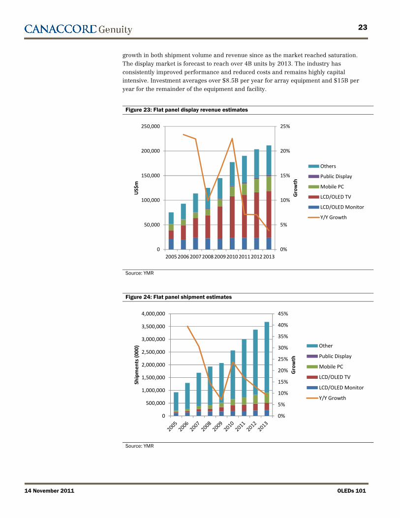
23
14 November 2011 OLEDs 101
growth in both shipment volume and revenue since as the market reached saturation. The display market is forecast to reach over 4B units by 2013. The industry has consistently improved performance and reduced costs and remains highly capital intensive. Investment averages over $8.5B per year for array equipment and $15B per year for the remainder of the equipment and facility.
Figure 23: Flat panel display revenue estimates
0%
5%
10%
15%
20%
25%
0
50,000
100,000
150,000
200,000
250,000
2005 2006 2007 2008 2009 2010 2011 2012 2013
Gro
wth
US$
m
Others
Public Display
Mobile PC
LCD/OLED TV
LCD/OLED Monitor
Y/Y Growth
Source: YMR
Figure 24: Flat panel shipment estimates
0%
5%
10%
15%
20%
25%
30%
35%
40%
45%
0
500,000
1,000,000
1,500,000
2,000,000
2,500,000
3,000,000
3,500,000
4,000,000
Gro
wth
Ship
men
ts (0
00) Other
Public Display
Mobile PC
LCD/OLED TV
LCD/OLED Monitor
Y/Y Growth
Source: YMR

24
OLEDs 101 14 November 2011
Much of these shipments are LCD but OLED technology has the potential to offer reduced costs and improve performance by replacing liquid crystal and the associated backlights, color filters, polarizers, alignment film and spacers with a mere seven to 10 very thin organic layers. This inherently simpler design and emissive technology offers the benefits of a thinner/lighter screen, lower power consumption and better contrast/picture. So far the higher cost vs. LCD is the biggest roadblock of OLED adoption. But with more aggressive scaling in moving from Gen 4 to Gen 5.5 and then even Gen 8 panel size, the cost is expected to come down rapidly.
LIGHTING INDUSTRY Lighting is a diverse, decentralized industry that generates billions of dollars per year. We calculate that the install base of the global Lighting market is composed of 22B fixtures comprising of 24B separate sockets in four major categories with hundreds of niche subcategories. Socket figures, the numbers we will refer to herein, are higher as some types of fixtures consist of more than one socket. We segment the fixture market into Residential, Commercial, Industrial and Outdoor, each composed of Incandescent, Compact Fluorescent (CFL), Fluorescent and High-Intensity Discharge (HID) technologies.
We calculate that there are 15B residential sockets; 6.5B commercial sockets; 1B industrial sockets; and 1B outdoor sockets. We calculate that residential fixtures have the capacity to produce 16,727,815 million lumens; commercial fixtures to produce 14,997,690 million lumens; industrial to produce 6,367,687 million lumens; and outdoor to produce 6,800,554 million lumens. Note that for the sake of this paper we are presenting our data worldwide, rather than regionally.

25
14 November 2011 OLEDs 101
Figure 25: 2010 lighting market
Calculated Sockets (M)
Calculated Lamps (M) Total Lumens (M)
Calculated Lumen-hrs (T)
11,141.8 9,489.1 10,027,608 10,248 1,120.0 122.6 1,008,000 1,104 2,754.6 452.4 5,509,189 9,049
45.8 11.1 183,018 668
15,062.136 10,075.304 16,727,815 21,069
1,540.1 4,497.1 1,386,090 6,071 735.2 268.3 882,240 3,864
4,051.2 709.8 11,343,360 49,684 138.6 24.3 1,386,000 6,071
6,465.100 5,499.493 14,997,690 65,690
105.9 502.5 95,310 678 186.1 110.4 223,376 1,590 713.6 203.2 3,568,000 25,395 165.4 47.1 2,481,000 17,659
1,171.047 863.156 6,367,687 45,322
165.4 603.6 148,838 543 349.3 106.2 391,216 1,428 322.5 98.1 967,500 3,531 529.3 128.8 5,293,000 19,319
1,366.476 936.756 6,800,554 24,822 24,064.8 17,374.710 44,893,746 156,903 21,682.4
Source: Canaccord Genuity
We estimate that the lighting opportunity will require a cumulative range of between 128.6B and 455.1B packaged LEDs between 2010 and 2020. These figures translate into penetration of the total lighting opportunity of a bearish cumulative penetration of 54.8% and a bullish 82.5% of the 2020 lighting install base, from less than 1% today. We believe the most likely scenario lies in between, which we are calling our base case. This base case will require a total of 249.3B LEDs and represent a ramp from 0.5% of the existing install base to 67.0% penetration of the 2020 install base.

26
OLEDs 101 14 November 2011
Figure 26: Estimated penetration of existing and new sockets
Total Cumulative WW Socket Penetration
0.0%
10.0%
20.0%
30.0%
40.0%
50.0%
60.0%
70.0%
80.0%
90.0%
100.0%
2010
2011
2012
2013
2014
2015
2016
2017
2018
2019
2020
Year
Bear
Base
Bull
Source: Canaccord Genuity estimates
The LED market is young but gaining traction and clearly expected to be disruptive given the data above. We do not expect the same levels of adoption for OLEDs. The OLED lighting market is further behind still, with few available commercial products, all of which are extremely expensive. These products tend to incorporate small 6” panels that wholesale for around $300, deliver 500 lm/m2, and have lifetimes (degradation to 70% of original output; known as “L70”) of 10,000 to 15,000 hours. While not terribly impressive, these products show good potential and can be found in the portfolios of Acuity, WAC, Philips, Osram and others.
Figure 27: OLED luminaires
Source: Acuity brands

27
14 November 2011 OLEDs 101
Key benefits of OLED lighting vs. some forms of traditional lighting include higher power efficiency as well as a flexible form factor. Because they can be deposited on a wide array of substrates, including transparent substrates, they provide a plethora of building integration options. While the cost is very high right now, ~100x or more compact fluorescent (CFL) lighting and ~10-15x for LED, the cost is expected to come down with more scale and improvements in technology. To be clear, OLEDs have a long way to go before they can challenge LEDs in performance and cost. These new OLED panels do not have performance advantages vs. LEDs and may never, but other intrinsic benefits could allow OLEDs to capture some niche markets, in our opinion.
Figure 28: Comparison of light source technology
Category Units OLED LED CFL Incandescent LFLColor Tunable Tunable White Warm WhiteCost Very High High Low Very Low LowEfficacy Lm/W 50-100 100-150 50-75 25-Oct 75-90Flexible Yes No No No NoForm Flexible/Rigid Rigid Rigid Rigid RigidLifetime L70 (000) 25-Oct 50 to 60 10 1 20-40Luminance Low Very High High Very High HighMaterials Organic Semi Compound Semi Mercury Vapor Tungsten Mercury VaporyProduct Maturity Very Low Medium High High High
Source AreaPoint; Area with
Diffusion Area Point AreaSwitching Speed Fast Fast Slow Slow SlowToxicity No No Yes- Mercury No Yes-MercuryTransparent Yes No No No No
Source: YMR
With OLED lighting in its infancy and the eventual specifications in flux, the following assumptions were made to forecast OLED penetration into the lighting market:
• Replacement lamps are not a good short/medium term application for OLEDs, due to the difference in form factor and the cost burden of fabricating a replacement bulb vs. a panel of light
• OLED luminaires represent a potential system cost savings, because like in the LCD industry, an OLED panel is simpler than many incumbent designs.
• Performance as forecasted in Figure 29

28
OLEDs 101 14 November 2011
Figure 29: OLED lighting performance forecast
Year cd/m2 lm/m2 lm/6" panel2010 769 2416 502011 1153 3624 752012 1910 6000 1242013 2387 7500 1552014 3183 10000 2072015 3979 12500 2592016 4775 15000 3102017 5570 17500 362
Source: YMR
While large area monolithic panels are possible with OLEDs, we believe that cost and scale issues for large area deposition will be limited to the high-end display market, and that lighting, which is more cost sensitive, will be better served by arrays of smaller OLED panels that may prove easier to manufacture. We forecast annual shipment volumes and revenue will transition to between 3.4M and 6.2M panels per year from less than 100,000 today, with revenues trending toward $200M - $400M by 2020. However note that this transition is predicated upon performance improvements, and increasing competition from the other solid state lighting technologies, LEDs. To compete with LEDs OLEDs must improve from:
• 2500 lumens/m2 in 2010 to 17,500 lumens/m2 in 2017
• $22,000/m2 in 2010 to < $500/m2 in 2017
• $500 per 6” panel in 2010 to $11 per 6” panel in 2017
We expect the largest jump in performance and manufacturing capacity to take place between 2015 and 2016, where we see a large pickup in shipments.

29
14 November 2011 OLEDs 101
Figure 30: Forecast of 6” OLED lighting panels
0
1
2
3
4
5
6
7
2011
2012
2013
2014
2015
2016
2017
2018
2019
2020
Shipmen
ts (M)
Bear
Base
Bull
Source: Canaccord Genuity
TECHNOLOGY OLED materials are complex chemicals, deposited in a stack of separate thin film layers. The configurations have evolved over time as manufacturers optimize the material structure to achieve the most saturated colors, the highest efficiency with the longest lifetime.
OLED materials are separated into two categories, small-molecule and large molecule, sometimes called polymer OLEDs (P-OLED). Small molecules are more advanced in terms of lifetime and efficiency and can be evaporated and deposited in a vacuum; however there is also work to develop solution processable small-molecule OLEDs. Most commercial OLED devices are based on small-molecule OLEDs. Large molecule OLEDs, pioneered by Cambridge Display Technology (later acquired by Sumitomo), were initially hyped due to their ability to be solution-processable. The benefit of this ability is that they can be dissolved in a solvent and deposited in an inkjet printing or spin coating techniques. While potentially cheaper to manufacture, the lifetimes and efficiencies suffer due to the interaction with the solvents.
The other major distinction is between Fluorescent or Phosphorescent emitter materials. Fluorescent materials were the earlier of the two, but suffer from a maximum theoretical efficiency of around 25%. Phosphorescent materials, originally developed by Princeton University and USC in the 1990s and exclusively licensed by Universal Display Corporation, have the theoretical ability to convert 100% of the internal quantum efficiency into light. Red phosphorescent materials have been available for years, green is just starting to be introduced but blue does not have the necessary lifetime currently.

30
OLEDs 101 14 November 2011
Material suppliers continue to make significant progress, however. Efficacy (cd/A) for red green and blue has improved by 200%, 300% and 50% concurrent with a very high improvement in lifetime and the ability to support a color gamut of 100% of the NTSC standard.
Figure 31: Light emitting material performance 2006 to 2011
2006
2011
Source: Source: LG Display, Universal Display
Structure The emitting layer for color displays consists of patterned red, green and blue light emitting material. Each light emitting layer consists of a host and a dopant. The dopant is the light emitting portion and is designed to release red, green or blue light. In the case of OLED lighting, the color patterning or pixelation is not required but white light is required. The white light is typically produced using three layers (red, green and blue) or two layers red/green and blue to reduce the process steps.
31
14 November 2011 OLEDs 101
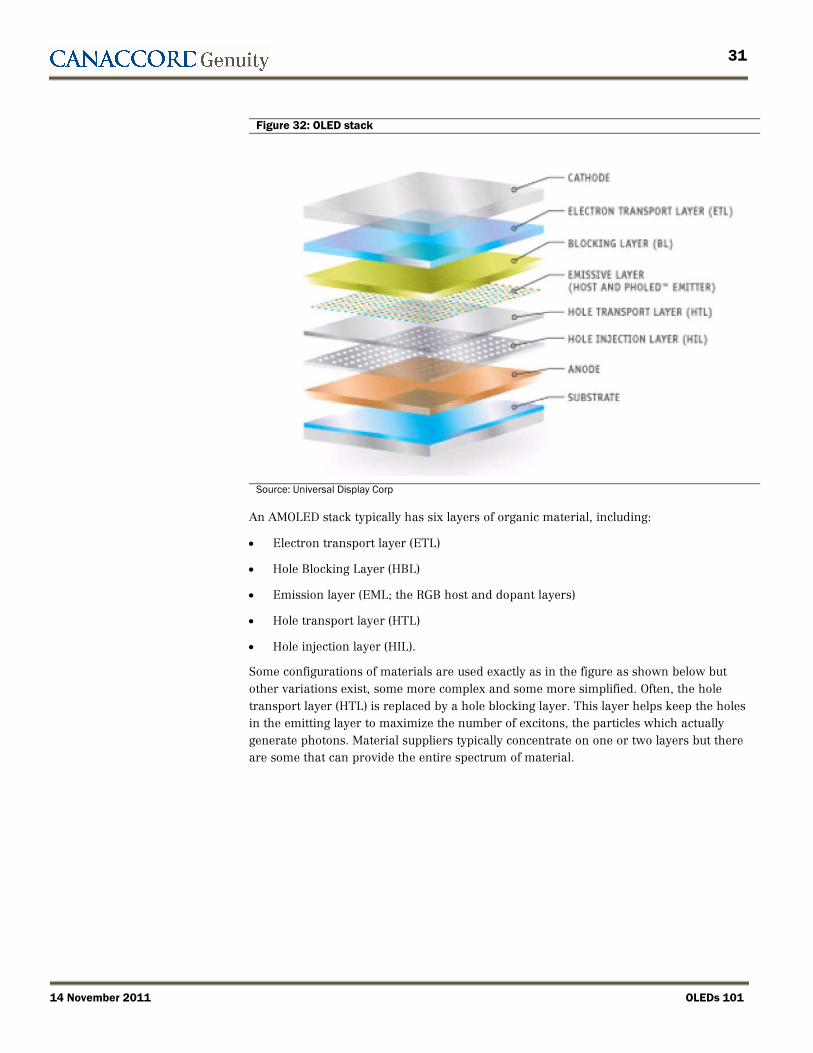
Figure 32: OLED stack
Source: Universal Display Corp
An AMOLED stack typically has six layers of organic material, including:
• Electron transport layer (ETL)
• Hole Blocking Layer (HBL)
• Emission layer (EML; the RGB host and dopant layers)
• Hole transport layer (HTL)
• Hole injection layer (HIL).
Some configurations of materials are used exactly as in the figure as shown below but other variations exist, some more complex and some more simplified. Often, the hole transport layer (HTL) is replaced by a hole blocking layer. This layer helps keep the holes in the emitting layer to maximize the number of excitons, the particles which actually generate photons. Material suppliers typically concentrate on one or two layers but there are some that can provide the entire spectrum of material.
32
OLEDs 101 14 November 2011
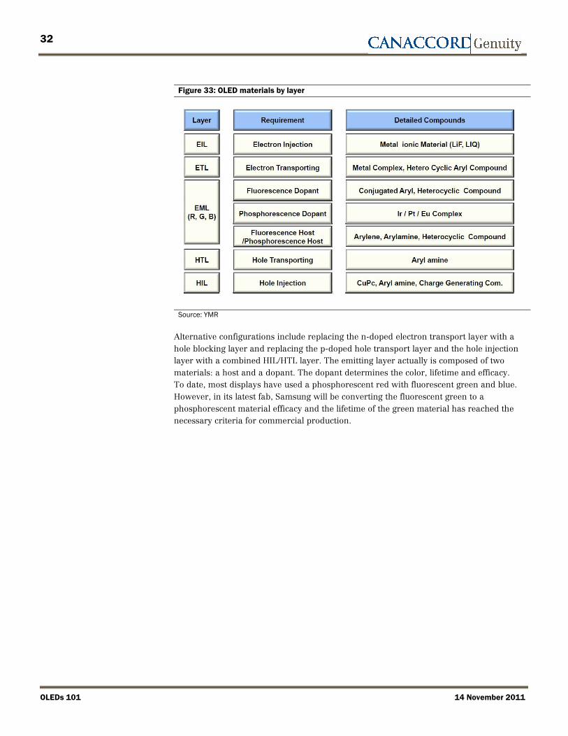
Figure 33: OLED materials by layer
Source: YMR
Alternative configurations include replacing the n-doped electron transport layer with a hole blocking layer and replacing the p-doped hole transport layer and the hole injection layer with a combined HIL/HTL layer. The emitting layer actually is composed of two materials: a host and a dopant. The dopant determines the color, lifetime and efficacy. To date, most displays have used a phosphorescent red with fluorescent green and blue. However, in its latest fab, Samsung will be converting the fluorescent green to a phosphorescent material efficacy and the lifetime of the green material has reached the necessary criteria for commercial production.

33
14 November 2011 OLEDs 101
Figure 34: OLED material
Source: Duksan Hi Metal
Figure 35 shows an alternative view of the configuration, plus the doped layers as proposed by Novaled. The doped layers replace the HIL, HTL and the ETL and EIL material. The anode uses ITO and the cathode uses aluminum. The EML is phosphorescent for red and green and fluorescent for blue.

34
OLEDs 101 14 November 2011
Figure 35: AMOLED configuration
Source: Duksan Hi Metal
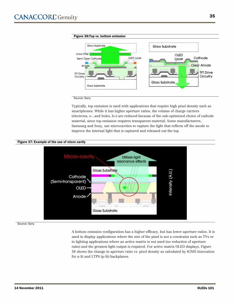
The stack can be designed to allow light to come out of the anode (bottom emission) or the cathode (top emission). In top emission light flows through the cathode, which is made from a transparent conductor such as indium tin oxide (ITO). In order to achieve the proper electrode emission, the ITO must be modified to include another metal. Excess light is reflected by a nontransparent anode or by using a micro cavity structure. The TFT array is under the anode, so that the TFT does not block the light. In a bottom emission structure light flows through the transparent anode, a portion of which is blocked by the TFT. Excess light is reflected by the non-transparent cathode.
35
14 November 2011 OLEDs 101
Figure 36:Top vs. bottom emission
Source: Sony
Typically, top emission is used with applications that require high pixel density such as smartphones. While it has higher aperture ratios, the volume of charge carriers (electrons, e-, and holes, h+) are reduced because of the sub-optimized choice of cathode material, since top emission requires transparent material. Some manufacturers, Samsung and Sony, use microcavities to capture the light that reflects off the anode to improve the internal light that is captured and released out the top.
Figure 37: Example of the use of micro cavity
Source: Sony
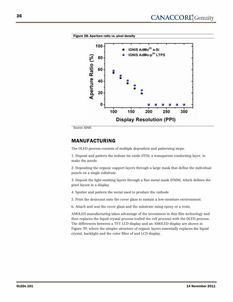
A bottom emission configuration has a higher efficacy, but has lower aperture ratios. It is used in display applications where the size of the pixel is not a constraint such as TVs or in lighting applications where an active matrix is not used (no reduction of aperture ratio) and the greatest light output is required. For active matrix OLED displays, Figure 38 shows the change in aperture ratio vs. pixel density as calculated by IGNIS Innovation for a-Si and LTPS (p-Si) backplanes.
36
OLEDs 101 14 November 2011
Figure 38: Aperture ratio vs. pixel density
Source: IGNIS
MANUFACTURING The OLED process consists of multiple deposition and patterning steps:
1. Deposit and pattern the indium tin oxide (ITO), a transparent conducting layer, to make the anode.
2. Depositing the organic support layers through a large mask that define the individual panels on a single substrate.
3. Deposit the light emitting layers through a fine metal mask (FMM), which defines the pixel layout in a display.
4. Sputter and pattern the metal used to produce the cathode
5. Print the desiccant onto the cover glass to sustain a low-moisture environment.
6. Attach and seal the cover glass and the substrate using epoxy or a resin.
AMOLED manufacturing takes advantage of the investment in thin film technology and then replaces the liquid crystal process (called the cell process) with the OLED process. The differences between a TFT LCD display and an AMOLED display are shown in Figure 39, where the simpler structure of organic layers essentially replaces the liquid crystal, backlight and the color filter of and LCD display.
37
14 November 2011 OLEDs 101
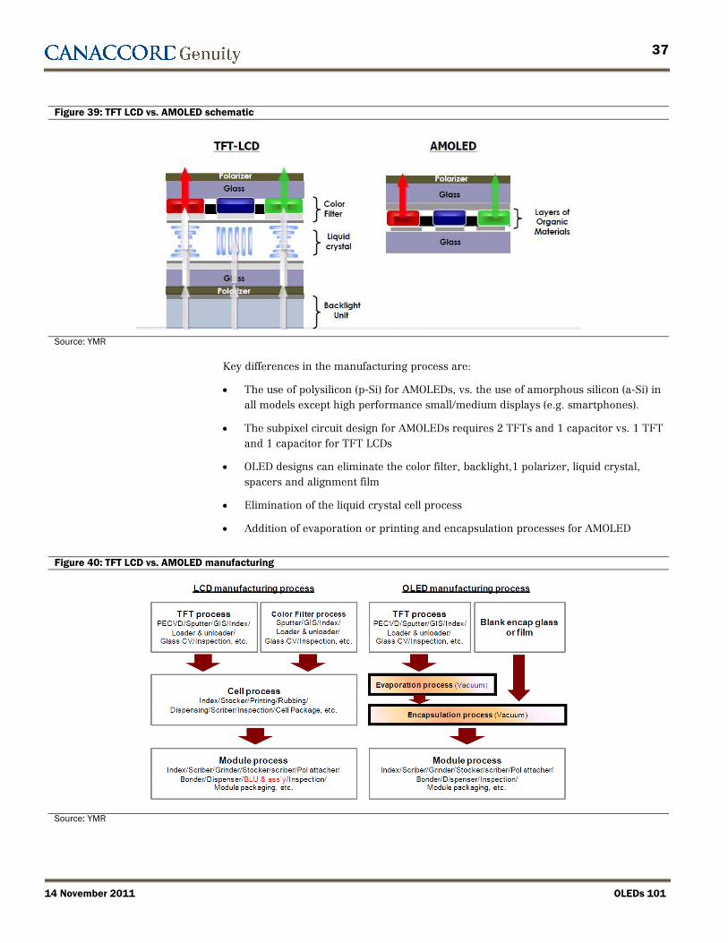
Figure 39: TFT LCD vs. AMOLED schematic
Source: YMR
Key differences in the manufacturing process are:
• The use of polysilicon (p-Si) for AMOLEDs, vs. the use of amorphous silicon (a-Si) in all models except high performance small/medium displays (e.g. smartphones).
• The subpixel circuit design for AMOLEDs requires 2 TFTs and 1 capacitor vs. 1 TFT and 1 capacitor for TFT LCDs
• OLED designs can eliminate the color filter, backlight,1 polarizer, liquid crystal, spacers and alignment film
• Elimination of the liquid crystal cell process
• Addition of evaporation or printing and encapsulation processes for AMOLED
Figure 40: TFT LCD vs. AMOLED manufacturing
Source: YMR

38
OLEDs 101 14 November 2011
Figure 41: Steps 1-3 deposition and FMM patterning
Source: YMM
Deposition and patterning
There are two approaches used to deposit organic materials on a substrate; 1) Vacuum Thermal Evaporation (VTE) and 2) Printing. To date the only method used in commercial production is VTE. The evaporation process condenses thin film layers on a glass substrate through vacuum evaporation of the organic matter. The evaporation step can be conducted in a low-pressure, hot-walled reactor chamber where organic materials are applied onto a cooled substrate. The RGB (red, green and blue) layers must then be patterned to form the individual pixels.
Surprisingly, depositing the organic material is not the most difficult step in the process as various tools already in industry meet the uniformity and throughput requirements. However, a much more difficult problem is the patterning of the red, green and blue light-emitting material into the subpixels. To produce these subpixels, a shadow mask called a fine metal mask (FMM) is used with the evaporation tool. The uniformity of the subpixel size determines the pixel density and the consistency of the color. For example, to achieve 200 pixels per inch, the maximum width of the subpixel is 41 µm, but to achieve the pixel density in Apple’s Retina Display, the maximum width drops down by 36% to 25 um. The subpixel width is further reduced by the need to leave room to separate the subpixels, typically 10% to 15% of the maximum width.
Figure 42: Subpixel maximum width by resolution
Ppi 200 300 327Max. Width 41 um 27um 25um
Source: YMR
To produce the subpixels, the FMM is placed between the evaporation source which contains the organic materials and the substrate. When the material is evaporated, it rises like steam and condenses either directly on the substrate (where the mask allows) or on the mask. Although this process is currently used by all display makers, it has some serious deficiencies:
• Material Utilization is quite low, averaging 3% to 5% depending on the particular equipment chosen, or inversely, material waste is 95% to 97%.

39
14 November 2011 OLEDs 101
• The masks are very expensive, must be cleaned after every 25-50 uses and then discarded after 200 uses. The cleaning and aligning process is time consuming and tends to reduce throughput.
• The mask process does not scale and to date the size is limited to 730x460mm. In order to scale, another process will have to be developed.
• It is limited to a minimum subpixel width of 40 um (~200 ppi)
Fortunately new processes which scale better are being developed. These include:
• Laser Induced Thermal Imaging (LITI) – a method of depositing light emitting material on a donor film and then using lasers to transfer the material from the film to the substrate.
• Printing – Using inkjet printing (IJP) or nozzle printing to deposit the material which becomes the subpixels.
• WOLED – Eliminating the pixelization process by producing white light using red, green and blue layers; achieve pixelization by applying a color filter on the cover glass.
• Small Mask Scan (SMS) – a method for larger displays, where the mask is held constant and the substrate move across it reducing the size of the mask and the subsequent sagging.
Figure 43: Deposition and patterning approaches
Source: Samsung
In a LITI process the red, green and blue material are vacuum first evaporated onto donor films. The donor films are then placed over the substrate and induced with a laser, causing the light emitting material to transfer from the film to the substrate.

40
OLEDs 101 14 November 2011
Figure 44: LITI process
Source: YMR
The RGBW (red, blue, green and white) configuration, developed by Kodak and later acquired by LG, deposits RGB light emitting materials, but does not pattern them, resulting in a uniform output of while light. This essentially creates a “backlight” which is then combined with a color filter to generate the individual pixels. This approach, minus the color filters/pixilation, is also what would be used to make OLED lighting panels.
The color filter is different than the one used for LCDs, because 1) different pigments are required to balance the colors produced by the OLEDs; and 2) because it includes a fourth white subpixel. The white subpixel is used to lower the power consumption because some of the gray scale can be produced by using one color and white instead of modulating the RGB subpixels. For example, to get pink with RGB all the colors must be used, but to get pink with RGBW, only red and white are required. The downside to this solution is 1) the cost of the color filter and 2) the lower efficacy, because the color filter absorbs 50% of the light.
Samsung and LG Display use the VTE/FMM process for the Gen 4.5 and Gen 5.5 fabs. VTE w/WOLED is practiced by both AUO and CMI. LG Display expects to use this approach for their Gen 8 TV fab. Nozzle printing is being developed by DuPont and Dai Nippon Screen. The joint venture is targeting Samsung’s Gen 8 for TVs as the first commercial installation. However, Samsung expects to use the SMS process for their pilot Gen 8.
The VTE with LITI process is being used by Samsung in the third phase of its Gen 5.5 phases and possibly for the Gen 8 TV process. LITI provides for very high pixel densities and has no apparent scaling limitations.

41
14 November 2011 OLEDs 101
Encapsulation
Sealing the finished OLED device properly prevents the absorption of humidity and oxygen which will destroy the light emitting materials. There are two approaches used to encapsulate these devices; 1) cover glass that is placed on top of the organic material and then sealed with epoxy or resins; 2) a thin film process where organic and inorganic layers are deposited directly on top of the organic material. To date, only the cover glass method is used. In early implementations a metal cover was used but was abandoned in favor of glass. Most encapsulation processes seal nitrogen in the OLED panels to prevent any potential damage from exposure to moisture and dust.
Figure 45: Alternative process flows for the OLED deposition and patterning
PrintingVTE w/FMM VTE w/o FMM (WOLED) VTE w/LITI
Sputter ITO--Anode
VTE HILw/Large Mask
VTE HTL w/Large Mas k
Al ign FMM
Evapora te Red
Al ign FMM
VTE Green
Align FMM
VTE Blue
Pa ttern ITO -- Anode
Clean Mask
Clean Ma sk
Clean Mask
Sputter ITO -- Anode
Pa ttern ITO -- Anode
VTE HBw/Large Mask
VTE ETL w/Large Mas k
VTE HILw/Large Mask
VTE HTL w/Large Mas k
VTE Red w/Large Mas k
VTE Green w/Large Mas k
VTE Blue w/Large Mas k
VTE HB w/Large Mas k
VTE ETL w/La rge Mas k
Sputter ITO--Anode
VTE HILw/Large Mask
VTE HTL w/La rge Mask
VTE Red on Donor Film
VTE Green on Donor Fi lm
La ser trnasfer Red Fm. Donor Film
La ser trnasfer Green Fm. Donor Film
Pa ttern ITO -- Anode
VTE Blue on Donor Fi lm
La ser trnasfer Red Fm. Donor Film
VTE HBw/Large Mask
VTE ETL w/Large Mas k
Sputter ITO --Anode
Pa ttern ITO --Anode
Print HIL
Print Red
Print Green
Print Blue
Print HB
Print ETL
Prep Glass
Source: YMR
Backplane The backplane array is the circuitry used to deliver the appropriate current level to the OLED stack. PMOLED and lighting backplanes are relatively simple and are similar. AMOLED backplanes use thin film technology originally developed for the LCD industry. By far the largest installed base of active matrix technology is amorphous silicon used for small/medium and large area displays with approximately 95% share. The remaining 5% of the LCD active matrix capacity uses low temperature polysilicon for high-end small/medium displays, where high pixel density and low power are required.
A PMOLED backplane uses a matrix of rows and columns made from a transparent conductor, typically ITO. At each intersection of the row and column a subpixel is addressed for the time allocated for one row. If a display has 100 rows and has a cycle

42
OLEDs 101 14 November 2011
time of 60Hz, the addressing time is ~16.7ms. The greater the number of rows, the less the addressing time. Once a particular row is addressed it will not be charged until all the other rows are addressed, in this case 983.3ms (one minus 16.7ms) – a relatively long time compared to the actual address time. The address time must be long enough that the eye does not see any changes between the on and off state. The maximum number of rows to meet this criterion is generally around 200 for OLEDs, given the amount of time the materials actually emit light once they are addressed. In order to get the voltage high enough to overcome the low persistence time, the voltage is driven 2 to 3 times higher than what would be used with an active matrix backplane. Therefore, not only is the size and resolution limited but the power consumption is higher for PMOLEDs. The benefit of PMOLEDs is the low capital cost, since no semiconductor processing is required to manufacture the backplane.
Lighting uses a similar technique, except that there is no need to pixelate the panel. Essentially, an OLED light is a single pixel driven by a passive matrix. In practice, the one pixel is divided into a low number of subpixels depending on the distance that the electrodes need to carry the voltage. In lighting, the method of delivering the voltage to the pixel is a metal grid composed of very thin conductors.
Figure 46: PMOLED architecture
Source: YMR
AMOLED The alternative backplane architecture, an active matrix, uses an array of thin film transistors (TFTs) originally developed for the LCD industry. Standard LCDs use amorphous silicon (a-Si) as the active material. High-resolution LCDs use polysilicon (p-Si) as the active material. The active material determines the speed at which an electron will flow. Amorphous Si has a mobility of 0.5-0.7 cm2/Vsec, while p-Si has a much higher mobility of 100 times greater (50 -200 cm2/vsec). For comparison purposes, single crystal silicon used in semiconductor ICs has a mobility value that is an order of magnitude higher still of 500 to 1,000 cm/Vsec.
Amorphous silicon transistors switch very slowly. We believe that premium displays will have to be at least 120 or 240 Hz range, which is how many times per second the image is refreshed. Going from 60Hz to 240 Hz for example allows only 1/4 of the time the electrons have to move through the transistors, favoring a solution with better electron mobility. Electron mobility also is a factor in determining the size of the transistor. Because OLEDs need a large amount of current, amorphous silicon pixels would have to be oversized relative to oxides or LTPS, limiting pixel density.
43
14 November 2011 OLEDs 101
Figure 47: Comparison of a-Si and p-Si
a-Si LTPS (p-Si) Comments
Capital Cost x 3xInvestment for p-Si is three times the cost of p-Si
Installed Base 95% 5%
a-Si is used in most LCD Fabs for small/medium and all LCD Fabs for large area displays
Pixel-to-Pixel Uniformity High LowAbility to maintain the same colorsaturation
Mobility Very Low MediumSpeed that the electron travels in the channel
Reliability Very Low MediumAbility of the TFT to maintain the Vth over time
Source: YMR
The difference between driving LCDs and OLEDs is that LCDs are voltage driven devices, while OLEDs are current driven devices, in other words an OLED pixel requires more current than an LCD pixel. This difference is manifested in the design of the subpixel circuit. For LCDs, one TFT and 1 capacitor are used per subpixel, whereas OLEDs require at least 2 TFTs: one to switch the subpixel on and off and the other to control the current level. When the row in an LCD is addressed, the TFT is turned on (High) and the voltage from the VDD electrode is used to charge the capacitor (Cs). When the row is deselected, the TFT is open (Low) and the capacitor and the LCD are connected in series, allowing the LCD to maintain the desired gray scale. The TFT is only used for 1/n sec, where n= the number of rows.
Figure 48: Basic LCD subpixel circuit (1T +1C)
CS
VDD
Sel
Sw.
LC
Source: YMR
The OLED subpixel circuit is more complex. It requires at least 2 TFTs and 1 capacitor.
The first TFT, SW, operates in a similar manner as the lone TFT in the LCD circuit. It is only on for 1/n sec, or approximately 1% of the time. The second TFT which controls the

44
OLEDs 101 14 November 2011
current and modulates the source VDD is on for almost the entire frame. The longer the TFT is on, the greater the difference in threshold voltage (Vth). As the threshold voltage changes, amorphous silicon heats up and loses its ability to properly drive current to the subpixel. Reducing this effect requires very large transistors. Polysilicon TFTs are better at managing threshold voltage shift, and can be made smaller due to their better electron mobility. The physical size and greater number of TFTs per subpixel basically render a-Si non-competitive for OLED backplanes. An added benefit of LTPS is that the driver ICs can be fabricated on the panel, reducing the cost of extra of driver ICs and allowing fewer connections.
Figure 49: Basic AMOLED subpixel circuit (2T +1C)
Vdata
CS
VDD
Sel
Sw.Dr.
OLED
Vdata
VDD
Sel
CS
Source: University of Stuttgart
The next figure shows a compensation circuit developed by Sony, which has 4TFTs and 1 capacitor. Samsung circuits use 6 TFTs and 1C. These additional compensation circuits adjust for:
• Voltage shifts for a-Si or metal oxide
• Correction for the “mura” issue (variations in brightness) for polysilicon

45
14 November 2011 OLEDs 101
• IR drop (the voltage drop across a resistance) for large displays
• Reduction of the effects of hysteresis, minimizing burn-in
• Aging of the OLED material for large displays
• OLED efficiency loss for large displays
The greater the number of TFTs, the better the performance of the AMOLED, however, there is a finite limit to the number of TFTs that will fit within the boundaries of the subpixel. For example, there is only room for 3 TFTs and 1C in the pixel density found in Apple’s Retina Display.
Figure 50: Sony 4 TFT 1C architecture
Idata
Sel 1
Sel 2
VDD
CS
Sw.
Sw.
Se. Dr.
OLED
Source: University of Stuttgart
As we indicated, polysilicon is a much better solution for the AMOLED backplane. However, its fabrication comes at a greater cost ($4-5M for each laser tool) and suffers from poor uniformity across the substrate. The most critical step in creating the LTPS backplane is the ELA (excimer laser annealing for crystallization) process in which a high-power laser beam is scanned across a layer of a-Si which on the substrate, aligning and crystallizing the silicon in the process. The figure below shows the conversion of a-Si to p-Si and the use of the laser beam.

46
OLEDs 101 14 November 2011
Figure 51: Polysilicon crystallization
Source: LG Display
The length of the laser beam had previously been limited to 365mm, which was designed for Gen 4.5 fabs, although recent breakthroughs have allowed the beam to be extended in size. The drawback is that as the laser beam is extended uniformity decreases, potentially to the point where the final circuit design may not be able to compensate. Furthermore, ELA slows the manufacturing process down. A typical Takt time in an a-Si LCD fab is 60 seconds. The multiple scans of the laser in the ELA process can take 2-3x longer.
Although the transistor array backplane for all of the OLED displays currently being manufactured use polysilicon ELA technology there are other approaches being studied, including:
• Super Grain Silicon (SGS): a method of using p-Si developed by Samsung (SMD).
• Amorphous- Solid Phase Crystallization (a-SPC): A process to convert a-Si to p-Si using annealing, which requires glass that can withstand higher temperatures
• Metal Oxide: A process that replaces a-Si with metal oxides, typically Indium Gallium Zinc Oxide.
While the ELA process requires extra steps and is more capex intensive, the other three approaches are still not proven.
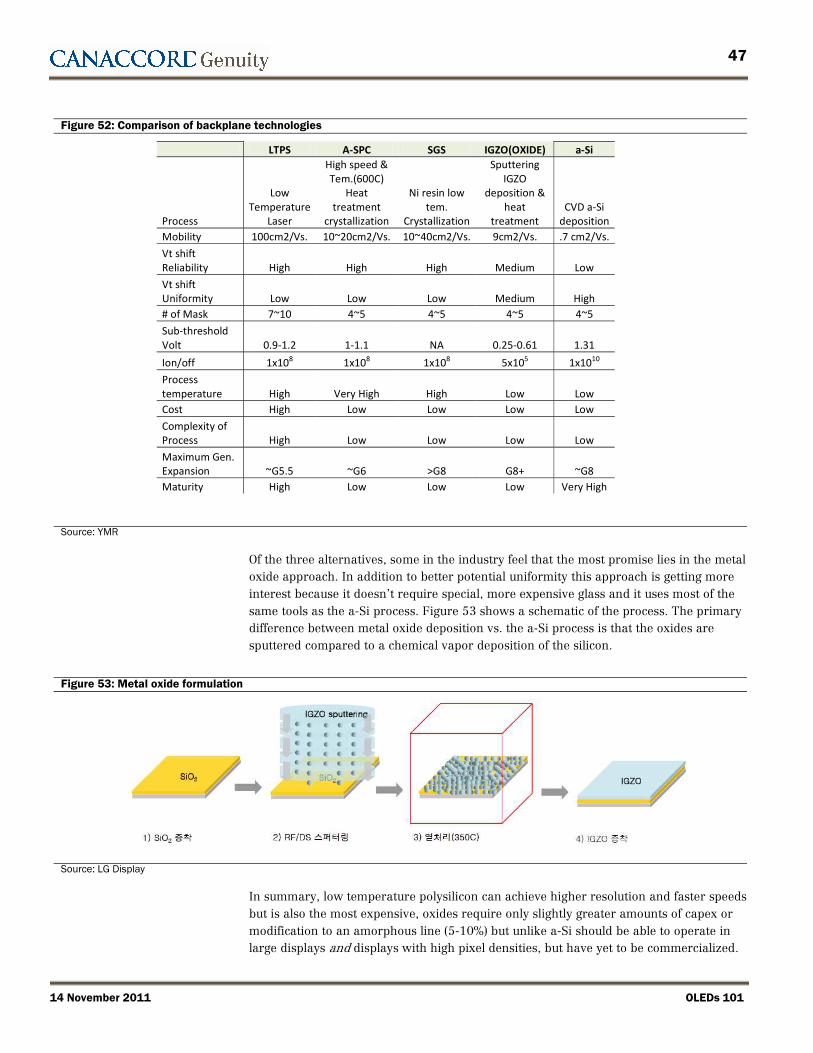
47
14 November 2011 OLEDs 101
Figure 52: Comparison of backplane technologies
LTPS A-SPC SGS IGZO(OXIDE) a-Si
Process
Low Temperature
Laser
High speed & Tem.(600C)
Heat treatment
crystallization
Ni resin low tem.
Crystallization
Sputtering IGZO
deposition & heat
treatment CVD a-Si
deposition Mobility 100cm2/Vs. 10~20cm2/Vs. 10~40cm2/Vs. 9cm2/Vs. .7 cm2/Vs.
Vt shift Reliability High High High Medium Low
Vt shift Uniformity Low Low Low Medium High # of Mask 7~10 4~5 4~5 4~5 4~5
Sub-threshold Volt 0.9-1.2 1-1.1 NA 0.25-0.61 1.31
Ion/off 1x10⁸ 1x10⁸ 1x10⁸ 5x10⁵ 1x10¹⁰
Process temperature High Very High High Low Low Cost High Low Low Low Low
Complexity of Process High Low Low Low Low
Maximum Gen. Expansion ~G5.5 ~G6 >G8 G8+ ~G8 Maturity High Low Low Low Very High
Source: YMR
Of the three alternatives, some in the industry feel that the most promise lies in the metal oxide approach. In addition to better potential uniformity this approach is getting more interest because it doesn’t require special, more expensive glass and it uses most of the same tools as the a-Si process. Figure 53 shows a schematic of the process. The primary difference between metal oxide deposition vs. the a-Si process is that the oxides are sputtered compared to a chemical vapor deposition of the silicon.
Figure 53: Metal oxide formulation
Source: LG Display
In summary, low temperature polysilicon can achieve higher resolution and faster speeds but is also the most expensive, oxides require only slightly greater amounts of capex or modification to an amorphous line (5-10%) but unlike a-Si should be able to operate in large displays and displays with high pixel densities, but have yet to be commercialized.
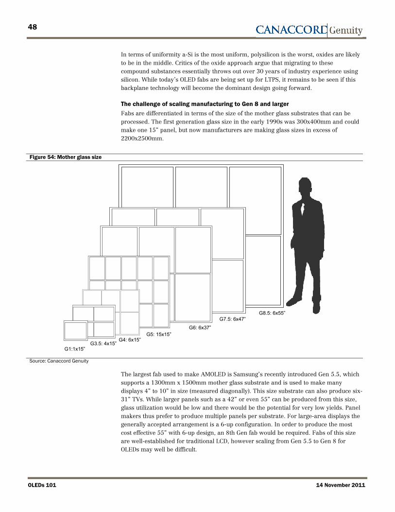
48
OLEDs 101 14 November 2011
In terms of uniformity a-Si is the most uniform, polysilicon is the worst, oxides are likely to be in the middle. Critics of the oxide approach argue that migrating to these compound substances essentially throws out over 30 years of industry experience using silicon. While today’s OLED fabs are being set up for LTPS, it remains to be seen if this backplane technology will become the dominant design going forward.
The challenge of scaling manufacturing to Gen 8 and larger Fabs are differentiated in terms of the size of the mother glass substrates that can be processed. The first generation glass size in the early 1990s was 300x400mm and could make one 15” panel, but now manufacturers are making glass sizes in excess of 2200x2500mm.
Figure 54: Mother glass size
G1:1x15”G3.5: 4x15”
G4: 6x15”G5: 15x15”
G6: 6x37”
G7.5: 6x47”G8.5: 6x55”
Source: Canaccord Genuity
The largest fab used to make AMOLED is Samsung’s recently introduced Gen 5.5, which supports a 1300mm x 1500mm mother glass substrate and is used to make many displays 4” to 10” in size (measured diagonally). This size substrate can also produce six- 31” TVs. While larger panels such as a 42” or even 55” can be produced from this size, glass utilization would be low and there would be the potential for very low yields. Panel makers thus prefer to produce multiple panels per substrate. For large-area displays the generally accepted arrangement is a 6-up configuration. In order to produce the most cost effective 55” with 6-up design, an 8th Gen fab would be required. Fabs of this size are well-established for traditional LCD, however scaling from Gen 5.5 to Gen 8 for OLEDs may well be difficult.
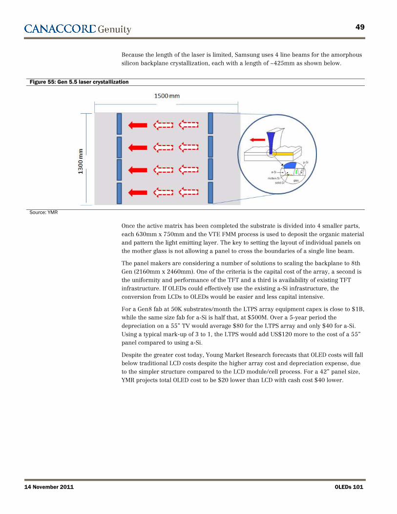
49
14 November 2011 OLEDs 101
Because the length of the laser is limited, Samsung uses 4 line beams for the amorphous silicon backplane crystallization, each with a length of ~425mm as shown below.
Figure 55: Gen 5.5 laser crystallization
Source: YMR
Once the active matrix has been completed the substrate is divided into 4 smaller parts, each 630mm x 750mm and the VTE FMM process is used to deposit the organic material and pattern the light emitting layer. The key to setting the layout of individual panels on the mother glass is not allowing a panel to cross the boundaries of a single line beam.
The panel makers are considering a number of solutions to scaling the backplane to 8th Gen (2160mm x 2460mm). One of the criteria is the capital cost of the array, a second is the uniformity and performance of the TFT and a third is availability of existing TFT infrastructure. If OLEDs could effectively use the existing a-Si infrastructure, the conversion from LCDs to OLEDs would be easier and less capital intensive.
For a Gen8 fab at 50K substrates/month the LTPS array equipment capex is close to $1B, while the same size fab for a-Si is half that, at $500M. Over a 5-year period the depreciation on a 55” TV would average $80 for the LTPS array and only $40 for a-Si. Using a typical mark-up of 3 to 1, the LTPS would add US$120 more to the cost of a 55” panel compared to using a-Si.
Despite the greater cost today, Young Market Research forecasts that OLED costs will fall below traditional LCD costs despite the higher array cost and depreciation expense, due to the simpler structure compared to the LCD module/cell process. For a 42” panel size, YMR projects total OLED cost to be $20 lower than LCD with cash cost $40 lower.

50
OLEDs 101 14 November 2011
Figure 56: Hypothetical cost structure (2015E)
OLED OLED OLED OLED panel costpanel costpanel costpanel cost Yielded Array Material Cost 46.278Yielded OLED Material Cost 103.501Yielded Encapsulation Material Cost 29.200Yielded Module Component Cost 44.252
Yielded Material and Component Total Cost 223.231Personnel Cost 6.918Depreciation + Building Cost 29.623Indirect Expense Total 19.780Warranty 3.228Manufacturing Total Cost 282.781Cash Cost 259.378
LCD LCD LCD LCD costcostcostcost Yielded Array Material Cost 37.078Yielded Cell Material Cost 87.702Yielded Module Component Cost 148.272
Yielded Material and Component Total Cost 273.051Personnel Cost 6.918Depreciation + Building Cost 11.002Indirect Expense Total 12.081Warrantee 3.572Manufacturing Total Cost 306.62Cash Cost 301.843
Source: Source: YMR
Samsung’s short term Gen8/55” TV solution is to use a similar technique for its gen Gen5.5 fab which uses the full Gen backplane and cuts the glass into smaller pieces for the OLED process. In this case it would cut the glass into 6 pieces, each one would be 720x1230 mm and would produce a 55” TV. The VTE and FMM process would obviously have to scale from the smaller substrate size of 630x750 mm in order for this to work. Unfortunately, the FMM begins to sag under its own weight when applied to the substrate horizontally – which poses a problem for the larger 720x1230 mask. Samsung is looking at using an approach being developed by SNU Precision that holds the substrate vertically to avoid sagging.
Samsung’s long-term solution is to manufacture the array from metal oxides using the a-Si infrastructure or a-SPC and the OLED stack using VTE w/LITI or nozzle printing using the DuPont/DNS approach.
LG Display is working on one overall solution to scale from their current Gen 4.5 to 8th Gen. They have announced the use of a metal oxide array and the RGBW OLED design which, as described above, does not require patterning.
PHYSICS OLEDs are semiconductor devices composed of carbon/hydrogen molecules that emit light when exposed to an electrical current. The basic physics are shown below. An electron (e-) is released from a metal layer designated as the cathode; a hole (h+) is released from a metal layer designated as the anode; when the electron and hole recombine in a light emitting layer an exciton is created and light is released.

51
14 November 2011 OLEDs 101
Figure 57: Organic semiconductor basics
e-
h+
Light
LUMO level (lowest unoccupied molecular orbital)
HOMO level (highest occupiedmolecular orbital)
Vacuum level
Electron energy
ExcitonLocalised on one molecule
Source: YMR
More specifically, the process of creating light consists of: 1) Injecting charge carriers (electrons and holes) into the device; 2)Transporting the charge carriers to the light emitting layer; 3)Recombining the charge carriers into excitons; and 4) Radiative decay leading to the emission of light. Note that the energy level of the exciton is less than the sum of the energy level of the charge carriers. The remaining energy is the radiative decay. For triplets with fluorescent material the non-radiative decay is released in the form of heat.

52
OLEDs 101 14 November 2011
Figure 58: Organic semiconductor basics: process steps
Source: YMR
Two types of excitons are possible: 1) Singlet, in which the Spin of the LUMO electron can pair with the spin of the HOMO electron. Both small molecule and polymer OLED materials contain singlets; 2) Triplet, in which the spin of the LUMO electron does not pair with the spin of the HOMO electron. These are only found in phosphorescent (organic metallic core) small molecule materials. The spin statistics suggest a 3:1 ratio of triplets to singlets, meaning triplets have more chances of recombining and creating light. As such phosphorescent materials are more efficient than fluorescent materials.
Inorganic light emitting diodes, or usually just “LEDs”, are also semiconductors that release light when current is applied. In theory, the process of creating light is similar, although the components are different. Charge carriers are released from the conduction band and the valence band of atoms and light is created with the energy of the material’s band gap. However the materials and manufacturing approach is very different between OLEDs and conventional inorganic LEDs, which are made in a mixed semiconductor process. Here multiple chemicals are reacted in a MOCVD tool and deposited onto a small sapphire or similar wafer. As we discussed above OLEDs are manufactured by depositing organic materials on a larger glass or plastic substrate using vacuum thermal evaporation or printing.

53
14 November 2011 OLEDs 101
Figure 6: Inorganic semiconductor process
e-
h+
LightFermi level
Conductor
electrons
holes
Band gap
Conduction band
Valence band
Vacuum level
Electron energy
Source: YMR
PERFORMANCE VS. LCDS AND TFT LCD While they are in their infancy, OLED displays hold the promise of performing better than LCDs in terms of contrast ratio, response time and form factor. Due to a simplified structure, the OLED displays should be less expensive to produce with the proper scale and investment. However, during the start-up phases of AMOLED manufacturing the volume is lower, the fabs are smaller and the yields are lower, resulting in a higher cost product. Even with these disadvantages, AMOLED displays used in smart phones have a price that is just 10% higher than comparable LCDs used in the iPhone, for example. Preliminary results from comparisons of early OLED models to LCDs have shown superiority in dark and light room contrast, pixel speed, weight (lightest), and power efficiency for video applications. LCDs continue to lead in resolution and display life.

54
OLEDs 101 14 November 2011
Figure 60: Comparing AMOLED, LCD, plasma and CRT
Source: Sony
Refresh rate, a measure of the speed that a pixel converts from on to off for a particular color is significant in video and in games where there are fast moving images. When the refresh rate is too slow, the display shows ghosting and distortion. The best LCDs switch in the low single digits of milli-seconds, while OLEDs switch in the low micro seconds (100x-1000x faster).
Figure 61: Pixel switching times
Source: Sony
Viewing angles, a measure of the change in contrast ratio as the user views the display from off-angles, is another important comparison metric. LCDs using twisted nematic (TN) type liquid crystal perform very poorly, and the contrast ratio can decline to 10:1 from 1,000:1. OLEDs claim contrast ratios that can maintain levels of 100,000:1 or more at similar viewing angles. However, LCD panel makers have adopted new approaches, such as in-plane switching and fringe field switching (to name a few) to improve the

55
14 November 2011 OLEDs 101
viewing angle. OLEDs may still hold the advantage against these new technologies, but the difference will be much smaller.
When an OLED and LCD display have the same luminance specification, e.g. 250 candela per square meter (cd/m2), to us the OLED display actually looks brighter as exhibited in Figure 62. The difference is caused by the higher contrast ratio and the higher color gamut for OLEDs. When measured in terms of color volume, the OLED is actually 40% brighter than a comparable LCD.
Figure 62: Comparison of OLED and TFT LCD display brightness
Source: Samsung
Color reproduction is a measure of the display’s ability to reproduce the color that the camera sees. As shown in Figure 63, both LCDs and OLEDs operate very effectively at the saturated level. However, when the requirement is reduced, for example skin tones, LCDs have very poor color reproduction in the range of 10% of what is requested. The cause of the poor performance is due to the color gamut of the LCD. An LCD has a very sharp gamma curve at the low gray scale levels so that it is difficult to interpret between two or three adjacent gray scales. OLEDs operate very effectively in the low gray scale range. Figure 64 shows the difference in the performance of LCDs and OLEDs in these low gray scale ranges. Because of its tight gamma curve, LCDs lose saturation as gray levels drop
Figure 63: Color reproduction at low gray scales
Source: Samsung

56
OLEDs 101 14 November 2011
Figure 64: Comparison of LCD and OLED displays operating in the low gray scale range
Source: Sony
Contrast measures the difference in luminance when a display shows a black image and when it shows a white image. OLED displays have been measured at less than 0.0002 cd/m2 for black, while LCDs have been measured at 0.07 cd/m2 because of light leakage. As a result OLED contrast ratios are in the range of 100,000 to 1,000,000:1, while traditional LCDs operate in the 10,000 to 15,000:1 range.
The comparison of power consumption for OLEDs and LCDs is complex because while LCDs have a common power rating, derived primarily from the backlight regardless of the image, OLED display power consumption is dependent on the image. For dark images OLEDs use a minimum amount of power, and for lighter images OLEDs use their maximum power. In between the extremes the difference between OLEDs and LCDs can vary widely. For movies, which generally average <18% gray scale the OLED uses 15% of the power that an LCD uses. For still images, OLEDs use 30% less power than LCDs. However, for most smartphone uses such as email, web searching and texting, OLEDs use more power because of the amount of white space on the image. Typically, an image that is 40% white is used as the key comparison and in this case OLEDs use 60% more power than an LCD.

57
14 November 2011 OLEDs 101
Figure 65: OLED and LCD power consumption based on image content
TFT LCD
AMOLED
100%
160%
TFT LCD
AMOLED
100%
15%
TFT LCD
AMOLED
100%
70%
White background MovieStill Image
Source: LG Display
OLED material suppliers have been improving the efficacy of the light emitting layers by an average of 15% per annum. The performance has improved from 15 cd/m2 in 2007 to 30 cd/m2 in 2011. It is projected that if the same level of performance continues, OLEDs and LCDs will be comparable at 40% white in a few years. Moreover, Samsung for example plans to convert to phosphorescent green in 2012 after having been using fluorescent greens in their displays. The use of phosphorescent green combined with the overall improvement, is forecasted by Samsung to reduce the power consumption by 25%.
Figure 66: Power consumption vs. time - 2007 to 2013E
’’’’08080808 ’’’’09090909 ’’’’10101010 ’’’’11111111 ’’’’12121212OLED : 3.7OLED : 3.7OLED : 3.7OLED : 3.7” WVGA 300 cd/m2 (40% Pixels On)WVGA 300 cd/m2 (40% Pixels On)WVGA 300 cd/m2 (40% Pixels On)WVGA 300 cd/m2 (40% Pixels On)’’’’0707070715 cd/A15 cd/A15 cd/A15 cd/A
LCD : 3.7LCD : 3.7LCD : 3.7LCD : 3.7” WVGA cd/m2 (100% Pixels On)WVGA cd/m2 (100% Pixels On)WVGA cd/m2 (100% Pixels On)WVGA cd/m2 (100% Pixels On)404 mW404 mW404 mW404 mW 252 mW252 mW252 mW252 mW
19 cd/A19 cd/A19 cd/A19 cd/A 20 cd/A20 cd/A20 cd/A20 cd/A 24 cd/A24 cd/A24 cd/A24 cd/A30 cd/A30 cd/A30 cd/A30 cd/A1,0001,0001,0001,000800800800800400400400400600600600600(mW)(mW)(mW)(mW)200200200200 ???? ’’’’13131313
Source: LG Display
MULTI-TOUCH TECHNOLOGY The Apple iPhone created a new demand for smartphones with a multi-touch capability that would allow: 1) Typing using a display in a similar manner to a physical keyboard; 2) Gestures allowing images (pictures) to be manipulated in size; and 3) A range of services to be selected by touching the panel.

58
OLEDs 101 14 November 2011
The multi-touch capability became so important that virtually no smartphone could be sold without it. There are many technologies used to enable touch including:
• Resistive
• Projected Capacitive
• Surface Capacitive
• Acoustic Infrared
• Embedded
Each has positives and negatives and is chosen to meet a specific set of needs. In 2010, the total touch market was $4.7B in revenue and 521M in units. The leading technology was projected capacitive as adopted by Apple with 279M units and revenues of $3.1B, a 54% and 67% share respectively. In implementing the first AMOLED smartphone displays, Samsung chose the same technique for OLEDs as was used for LCDs and is shown in the next figure. This approach uses a glass or plastic layer onto which is orthogonally patterned transparent conductors (TCO) on either side. The TCO is typically made of Indium Tin Oxide (ITO). In addition to the glass or plastic layer, an A/D converter and a DSP are required to 1) read the location of the touch(s) and 2) interpret the gestures. The ICs are typically available from a number of sources.
Figure 67: Projected capacitive touch
Source: SID -- Geoff Walker
The projected capacitive approach as developed by Apple and shown in the next figure uses the controller to measure capacitance between two electrodes as opposed to an earlier version, which measures the capacitance to ground of a single electrode.

59
14 November 2011 OLEDs 101
Figure 68: Mutual capacitance
Source: SID -- Geoff Walker
The glass or plastic layer is placed on top of the display and the ICs are then connected to the smartphones CPU. This approach works for the TFT LCDs and for AMOLEDs but for AMOLEDs, the space between the touch layer and the display causes the external light to bounce between the two layers and exaggerates the ambient light making the OLED virtually unreadable in high ambient light conditions. The LCD does not suffer from this problem.
Samsung developed a solution in which 0.001mm-thick capacitive touch sensors are deposited between the panel's substrate and the top polarizer film for top emission, thus removing the usual touchscreen glass cover and the gap that it creates. Samsung, called this approach on-cell touch and the displays are labeled Super AMOLEDs. The next figure shows how the touch sensor is placed between the OLED and the polarizer. Since there is no layer on top of the display, there is no space and no light scattering between the layers. Therefore, the performance in high ambient light conditions is much improved.
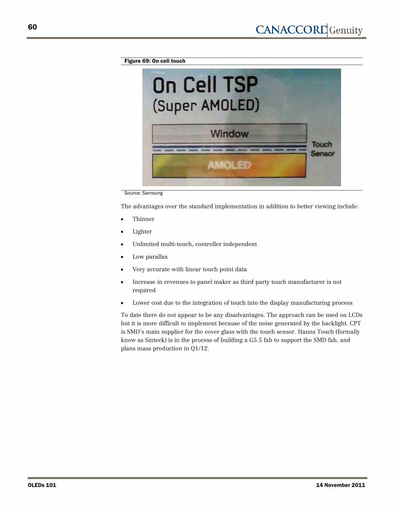
60
OLEDs 101 14 November 2011
Figure 69: On cell touch
Source: Samsung
The advantages over the standard implementation in addition to better viewing include:
• Thinner
• Lighter
• Unlimited multi-touch, controller independent
• Low parallax
• Very accurate with linear touch point data
• Increase in revenues to panel maker as third party touch manufacturer is not required
• Lower cost due to the integration of touch into the display manufacturing process
To date there do not appear to be any disadvantages. The approach can be used on LCDs but it is more difficult to implement because of the noise generated by the backlight. CPT is SMD’s main supplier for the cover glass with the touch sensor. Hanns Touch (formally know as Sinteck) is in the process of building a G5.5 fab to support the SMD fab, and plans mass production in Q1/12.

61
14 November 2011 OLEDs 101
APPENDIX: IMPORTANT DISCLOSURES Analyst Certification: Each authoring analyst of Canaccord Genuity whose name appears on the front page of this investment
research hereby certifies that (i) the recommendations and opinions expressed in this investment research accurately reflect the authoring analyst’s personal, independent and objective views about any and all of the designated investments or relevant issuers discussed herein that are within such authoring analyst’s coverage universe and (ii) no part of the authoring analyst’s compensation was, is, or will be, directly or indirectly, related to the specific recommendations or views expressed by the authoring analyst in the investment research.
Distribution of Ratings: Global Stock Ratings (as of 4 November 2011)
Coverage UniverseCoverage UniverseCoverage UniverseCoverage Universe IB ClientsIB ClientsIB ClientsIB Clients RatingRatingRatingRating #### %%%% %%%% Buy 494 63.3% 36.4% Speculative Buy 83 10.6% 68.7% Hold 192 24.6% 18.2% Sell 12 1.5% 16.7% 781 100%
Canaccord Ratings System:
BUY:BUY:BUY:BUY: The stock is expected to generate risk-adjusted returns of over 10% during the next 12 months. HOLD:HOLD:HOLD:HOLD: The stock is expected to generate risk-adjusted returns of 0-10% during the next 12 months. SELL:SELL:SELL:SELL: The stock is expected to generate negative risk-adjusted returns during the next 12 months. NOT RATED:NOT RATED:NOT RATED:NOT RATED: Canaccord Genuity does not provide research coverage of the relevant issuer. “Risk-adjusted return” refers to the expected return in relation to the amount of risk associated with the designated investment or the relevant issuer.
Risk Qualifier: SPECULATIVSPECULATIVSPECULATIVSPECULATIVE:E:E:E: Stocks bear significantly higher risk that typically cannot be valued by normal fundamental
criteria. Investments in the stock may result in material loss. Canaccord Genuity is the business name used by certain subsidiaries of Canaccord Financial Inc., including
Canaccord Genuity Inc., Canaccord Genuity Limited, and Canaccord Genuity Corp. The authoring analysts who are responsible for the preparation of this investment research are employed by Canaccord Genuity Corp. a Canadian broker-dealer with principal offices located in Vancouver, Calgary, Toronto, Montreal, or Canaccord Genuity Inc., a US broker-dealer with principal offices located in Boston, New York, San Francisco and Houston or Canaccord Genuity Limited., a UK broker-dealer with principal offices located in London and Edinburgh (UK). In the event that this is compendium investment research (covering six or more relevant issuers), Canaccord Genuity and its affiliated companies may choose to provide specific disclosures of the subject companies by reference, as well as its policies and procedures regarding the dissemination of investment research. To access this material or for more information, please send a request to Canaccord Genuity Research, Attn: Disclosures, P.O. Box 10337 Pacific Centre, 2200-609 Granville Street, Vancouver, BC, Canada V7Y 1H2 or [email protected]. The authoring analysts who are responsible for the preparation of this investment research have received (or will receive) compensation based upon (among other factors) the Corporate Finance/Investment Banking revenues and general profits of Canaccord Genuity. However, such authoring analysts have not received, and will not receive, compensation that is directly based upon or linked to one or more specific Corporate Finance/Investment Banking activities, or to recommendations contained in the investment research. Canaccord Genuity and its affiliated companies may have a Corporate Finance/Investment Banking or other relationship with the company that is the subject of this investment research and may trade in any of the designated investments mentioned herein either for their own account or the accounts of their customers, in good faith or in the normal course of market making. Accordingly, Canaccord Genuity or their affiliated companies, principals or employees (other than the authoring analyst(s) who prepared this investment research) may at any time have a long or short position in any such designated investments, related designated investments or in options, futures or other derivative instruments based thereon. Some regulators require that a firm must establish, implement and make available a policy for managing conflicts of interest arising as a result of publication or distribution of investment research. This investment research has been prepared in accordance with Canaccord Genuity’s policy on managing conflicts of interest, and information barriers or firewalls have been used where appropriate. Canaccord Genuity’s policy is available upon request. The information contained in this investment research has been compiled by Canaccord Genuity from sources believed to be reliable, but (with the exception of the information about Canaccord Genuity) no representation or warranty, express or implied, is made by Canaccord Genuity, its affiliated companies or any other person as to its fairness, accuracy, completeness or correctness. Canaccord Genuity has not independently verified the facts, assumptions, and estimates contained herein. All estimates, opinions and other information contained in this investment research constitute Canaccord Genuity’s judgement as of the date of this investment research, are subject to change without notice and are provided in good faith but without legal

62
OLEDs 101 14 November 2011
responsibility or liability. Canaccord Genuity’s salespeople, traders, and other professionals may provide oral or written market commentary or trading strategies to our clients and our proprietary trading desk that reflect opinions that are contrary to the opinions expressed in this investment research. Canaccord Genuity’s affiliates, principal trading desk, and investing businesses may make investment decisions that are inconsistent with the recommendations or views expressed in this investment research. This investment research is provided for information purposes only and does not constitute an offer or solicitation to buy or sell any designated investments discussed herein in any jurisdiction where such offer or solicitation would be prohibited. As a result, the designated investments discussed in this investment research may not be eligible for sale in some jurisdictions. This investment research is not, and under no circumstances should be construed as, a solicitation to act as a securities broker or dealer in any jurisdiction by any person or company that is not legally permitted to carry on the business of a securities broker or dealer in that jurisdiction. This material is prepared for general circulation to clients and does not have regard to the investment objectives, financial situation or particular needs of any particular person. Investors should obtain advice based on their own individual circumstances before making an investment decision. To the fullest extent permitted by law, none of Canaccord Genuity, its affiliated companies or any other person accepts any liability whatsoever for any direct or consequential loss arising from or relating to any use of the information contained in this investment research.
For Canadian Residents: This Investment Research has been approved by Canaccord Genuity Corp., which accepts sole responsibility
for this Investment Research and its dissemination in Canada. Canadian clients wishing to effect transactions in any Designated Investment discussed should do so through a qualified salesperson of Canaccord Genuity Corp. in their particular jurisdiction.
For United Kingdom Residents:
This investment research is distributed in the United Kingdom, as third party research by Canaccord Genuity Limited, which is authorized and regulated by the Financial Services Authority. This research is for distribution only to persons who are Eligible Counterparties or Professional Clients only and is exempt from the general restrictions in section 21 of the Financial Services and Markets Act 2000 on the communication of invitations or inducements to engage in investment activity on the grounds that it is being distributed in the United Kingdom only to persons of a kind described in Article 19(5) (Investment Professionals) and 49(2) (High Net Worth companies, unincorporated associations etc) of the Financial Services and Markets Act 2000 (Financial Promotion) Order 2005 (as amended). It is not intended to be distributed or passed on, directly or indirectly, to any other class of persons. This material is not for distribution in the United Kingdom to retail clients, as defined under the rules of the Financial Services Authority.
For United States Residents:
Canaccord Genuity Inc., a US registered broker-dealer, accepts responsibility for this Investment Research and its dissemination in the United States. This Investment Research is intended for distribution in the United States only to certain US institutional investors. US clients wishing to effect transactions in any Designated Investment discussed should do so through a qualified salesperson of Canaccord Genuity Inc. Analyst(s) preparing this report that are not employed by Canaccord Genuity Inc are resident outside the United States and are not associated persons or employees of any US regulated broker-dealer. Such analyst(s) may not be subject to Rule 2711 restrictions on communications with a subject company, public appearances and trading securities held by a research analyst account.
For European Residents: If this Investment Research is intended for disclosure in any jurisdiction other than the United Kingdom, the
US or Canada, then the relevant rules and regulatory requirements of that jurisdiction will apply. Additional information is available on request.Additional information is available on request.Additional information is available on request.Additional information is available on request.
Copyright © Canaccord Genuity Corp. 2011. – Member IIROC/Canadian Investor Protection Fund Copyright © Canaccord Genuity Limited 2011. – Member LSE, authorized and regulated by the Financial Services Authority. Copyright © Canaccord Genuity Inc. 2011. – Member FINRA/SIPC All rights reserved. All material presented in this document, unless specifically indicated otherwise, is under copyright to Canaccord Genuity Corp., Canaccord Genuity Limited, and Canaccord Genuity Inc. None of the material, nor its content, nor any copy of it, may be altered in any way, or transmitted to or distributed to any other party, without the prior express written permission of the entities listed above.