nanoimprint materials - sematech almaden research center 3 sematech litho forum 05/24/2006 © 2003...
TRANSCRIPT
IBM Almaden Research Center
05/24/2006 © 2003 IBM Corporation
NanoImprint Materials
March, 2006
Ratnam Sooriyakumaran
Hiroshi Ito
Mark Hart
Frances Houle
Geraud Dubois
Robert Miller
Robert Allen

IBM Almaden Research Center
© 2003 IBM Corporation2 Sematech Litho Forum 05/24/2006
Imprint in IBM
IBM Research Division is conducting an exploratory project on Materials for Imprint Lithography and Applications.
This is not part of IBM’s Semiconductor Lithography Roadmap.
IBM Almaden Research Center
© 2003 IBM Corporation3 Sematech Litho Forum 05/24/2006
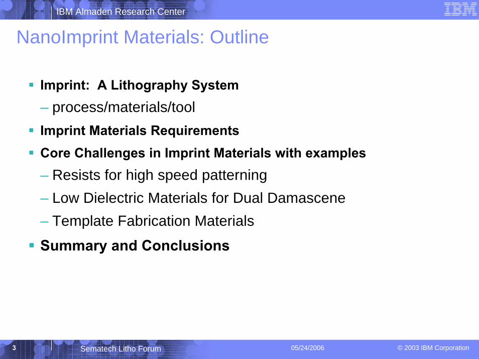
NanoImprint Materials: Outline
Imprint: A Lithography System – process/materials/toolImprint Materials RequirementsCore Challenges in Imprint Materials with examples– Resists for high speed patterning– Low Dielectric Materials for Dual Damascene– Template Fabrication Materials
Summary and Conclusions

IBM Almaden Research Center
© 2003 IBM Corporation4 Sematech Litho Forum 05/24/2006
Litho Metrics Tool Impact Material Impact Template Impact Etcher Impact
Resolution HIGH LOW HIGH
HIGH
HIGH
Defects HIGH HIGH HIGH LOW
Throughput HIGH HIGH LOW LOW
LOW
CD control HIGH LOW LOW
Overlay HIGH LOW LOW
TOOLMATERIAL TEMPLATE ETCHER F
DEVELOP
Imprint: The System (thanks to Molecular Imprints!)OR DRY
IBM Almaden Research Center
© 2003 IBM Corporation5 Sematech Litho Forum 05/24/2006
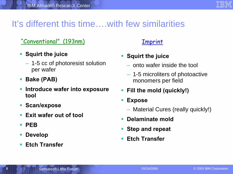
It’s different this time….with few similarities
Squirt the juice– 1-5 cc of photoresist solution
per wafer
Bake (PAB)Introduce wafer into exposure toolScan/exposeExit wafer out of toolPEBDevelopEtch Transfer
Squirt the juice– onto wafer inside the tool– 1-5 microliters of photoactive
monomers per field
Fill the mold (quickly!)Expose– Material Cures (really quickly!)
Delaminate moldStep and repeatEtch Transfer
“Conventional” (193nm) Imprint
IBM Almaden Research Center
© 2003 IBM Corporation6 Sematech Litho Forum 05/24/2006
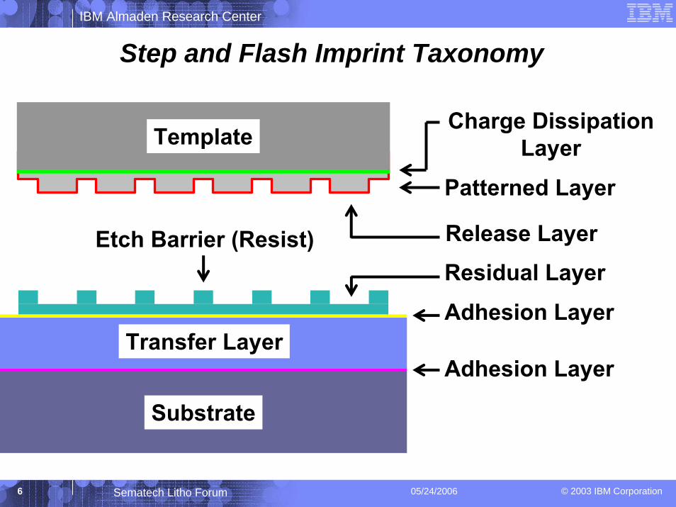
Step and Flash Imprint Taxonomy
Template
Substrate
Transfer Layer
Etch Barrier (Resist)
Adhesion Layer
Adhesion Layer
Release LayerResidual Layer
Patterned Layer
Charge DissipationLayer

IBM Almaden Research Center
© 2003 IBM Corporation7 Sematech Litho Forum 05/24/2006
Interface energetics and stability in UV-cure nanoimprintlithography: potential sources of defectivity
Resist adhesion to template despite release layer
polymer
Release layer
Cured resist
Failure of resist to wet surfaces
Cohesive failure of resist
Adhesion failure
template
silicon

IBM Almaden Research Center
© 2003 IBM Corporation8 Sematech Litho Forum 05/24/2006
Imprint Materials Requirements
Low Viscosity Required for high fill rates
Proper Surface Tension and compatibility with release coating
High speed cure (for low dwell times)
Low adhesive forces after cure (Clean Release)
Proper Mechanical Properties after cure?
Etch Resistance for pattern transfer– In resist (Si Resist)
– In planarization material (reverse tone process)

IBM Almaden Research Center
© 2003 IBM Corporation9 Sematech Litho Forum 05/24/2006
Core Challenges: Materials for NIL
Sacrificial (resist) layers
Image reversal materials
Permanent Materials (e.g., Dual Damascene ILD Material)
Template fabrication materials
Materials
fundamentalsHigh Performance Release (Low Defectivity)
Durability of release coating
Control/robustness of surfaces
IBM Almaden Research Center
© 2003 IBM Corporation10 Sematech Litho Forum 05/24/2006
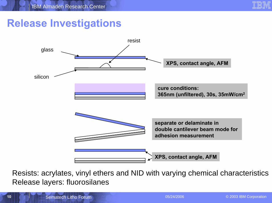
Release Investigations
glass
cure conditions:365nm (unfiltered), 30s, 35mW/cm2
separate or delaminate in double cantilever beam mode for adhesion measurement
XPS, contact angle, AFM
XPS, contact angle, AFM
resist
silicon
Resists: acrylates, vinyl ethers and NID with varying chemical characteristicsRelease layers: fluorosilanes
IBM Almaden Research Center
© 2003 IBM Corporation11 Sematech Litho Forum 05/24/2006
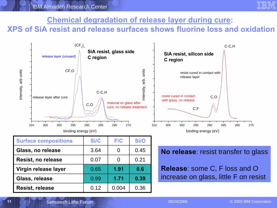
Chemical degradation of release layer during cure: XPS of SiA resist and release surfaces shows fluorine loss and oxidation
No release: resist transfer to glass
Release: some C, F loss and O increase on glass, little F on resist
310 305 300 295 290 285 280 275
CF,O
(CF2)x
C,O
C-C,H
SiA resist, glass sideC region
release layer after cure
release layer (unused)
material on glass after cure, no release treatment
inte
nsity
, arb
uni
ts
binding energy (eV)310 305 300 295 290 285 280 275
C,F
C,O
C-C,H
resist cured in contactwith glass, no release
SiA resist, silicon sideC region
resist cured in contact withrelease layer
inte
nsity
, arb
. uni
ts
binding energy (eV)
Surface compositions Si/C F/C Si/O
Glass, no release 3.64 0
0
1.91
1.71
0.004
0.45
Resist, no release 0.07 0.21
Virgin release layer 0.65 0.6
Glass, release 0.99 0.39
Resist, release 0.12 0.36
IBM Almaden Research Center
© 2003 IBM Corporation12 Sematech Litho Forum 05/24/2006
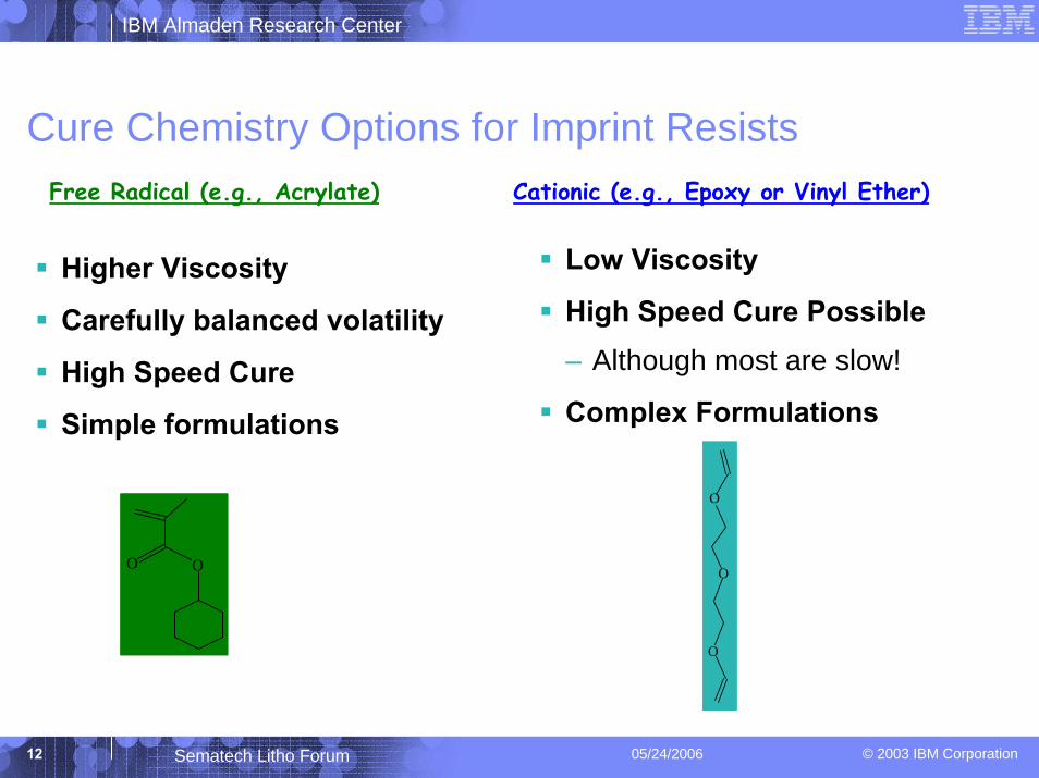
Cure Chemistry Options for Imprint Resists
Higher Viscosity
Carefully balanced volatility
High Speed Cure
Simple formulations
Low Viscosity
High Speed Cure Possible– Although most are slow!
Complex Formulations
Free Radical (e.g., Acrylate) Cationic (e.g., Epoxy or Vinyl Ether)
OO
O
O
O
IBM Almaden Research Center
© 2003 IBM Corporation13 Sematech Litho Forum 05/24/2006
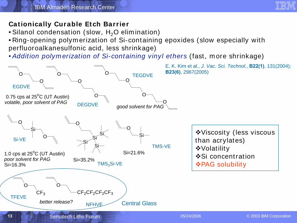
Cationically Curable Etch Barrier•Silanol condensation (slow, H2O elimination)•Ring-opening polymerization of Si-containing epoxides (slow especially with perfluoroalkanesulfonic acid, less shrinkage)•Addition polymerization of Si-containing vinyl ethers (fast, more shrinkage)
Viscosity (less viscous than acrylates)
VolatilitySi concentrationPAG solubility
OO
OO
O
OO
OO
SiO
O
O
SiSi
SiSi
1.0 cps at 25oC (UT Austin)poor solvent for PAGSi=16.3%
Si=35.2%
OCF3
0.75 cps at 25oC (UT Austin)volatile, poor solvent of PAG
good solvent for PAG
better release?
OSi
OCF2CF2CF2CF3
Si=21.6%
EGDVE
DEGDVE
TEGDVE
Si-VE
TMS3Si-VE
TMS-VE
TFEVENFHVE Central Glass
E. K. Kim et al., J. Vac. Sci. Technol., B22(1), 131(2004);B23(6), 2967(2005)
IBM Almaden Research Center
© 2003 IBM Corporation14 Sematech Litho Forum 05/24/2006
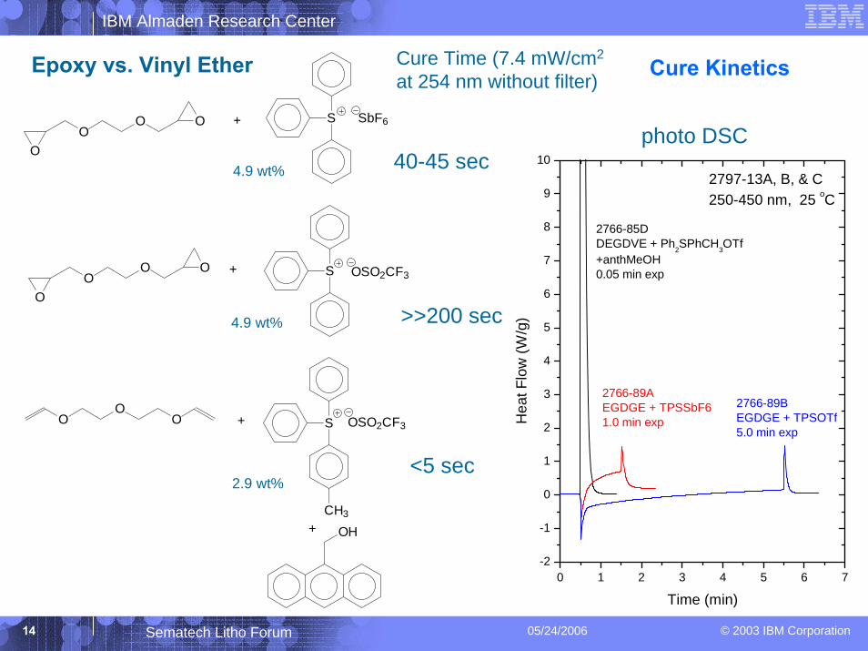
Epoxy vs. Vinyl Ether
OO
O O
OO
O O
S
S
SbF6
OSO2CF3
+
+
OO
O S
CH3
OSO2CF3+
OH+
Cure Time (7.4 mW/cm2
at 254 nm without filter)
40-45 sec
>>200 sec
<5 sec
4.9 wt%
4.9 wt%
2.9 wt%
0 1 2 3 4 5 6 7-2
-1
0
1
2
3
4
5
6
7
8
9
10
2766-89BEGDGE + TPSOTf5.0 min exp
2766-89AEGDGE + TPSSbF61.0 min exp
2766-85DDEGDVE + Ph2SPhCH3OTf+anthMeOH0.05 min exp
2797-13A, B, & C250-450 nm, 25 oC
Hea
t Flo
w (W
/g)
Time (min)
photo DSCEGDGE
DEGDVE
Cure Kinetics

IBM Almaden Research Center
© 2003 IBM Corporation15 Sematech Litho Forum 05/24/2006
AMRC Project on Low-k Dielectric Materials for NIL Grant Willson and team working with IBM Research – (Scope—ILD NIL Materials and Processes for back-end process
simplification)….can NIL be used for semiconductor processing?Almaden Team represented by Mark Hart—Assignee to AMRC/Nanoimprint—Lithography Experiments @ UTMark is backed up by chemists in 3 groups at Almaden– Low-k team (characterization and new materials designs)– Resist (litho materials) Team (Silicon Chemistry)– SDL (Formulation Scale-up)
Willson Group has NanoImprint experienceIBM supplying initial materials to UT with new designIBM supplying low-k know-how and characterization Exchange of personnel for future materials directions
IBM Research Assignee: Mark W. Hart
(External Programs (7/05–1/06), Lithography (1/06–7/06))

IBM Almaden Research Center
© 2003 IBM Corporation16 Sematech Litho Forum 05/24/2006
M. Neisser et. al, Solid State Technology’
August 2000, Pp.127-132
Up to 18 steps
Current Dual-Damascene Integration Scheme Template
POSS Deriva
Patterned Wa
Dispense
Press and Photocure
Release
High TempThermal cure
BreakthroughEtch
CMP
MetalDeposition
Our Proposed Integration Scheme Why NIL for Integration?

IBM Almaden Research Center
© 2003 IBM Corporation17 Sematech Litho Forum 05/24/2006
Photocurable Dielectric Material Requirements
Property/Characteristic
Low Viscosity
Photocurable
Cure Shrinkage
Dielectric Constant
Thermal Stability
Mechanical Properties
CTE
Water Sorption
Requirement
Less than 50 cPs
Fast Chain polymerization
Less than 15%
ε ≤ 3
Less than 1% wt loss/hr @ 400oC
Young’s Modulus ≥ 5 GPa
Less than 25 ppm/oC
Less than 0.5% wt
IBM Almaden Research Center
© 2003 IBM Corporation18 Sematech Litho Forum 05/24/2006
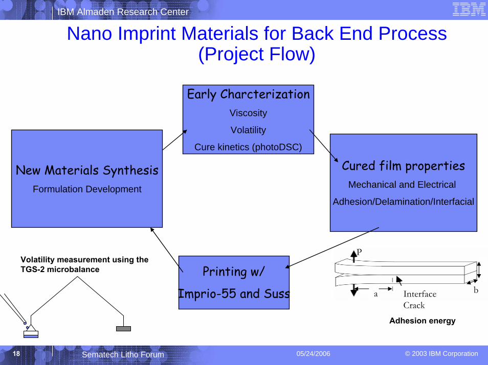
Nano Imprint Materials for Back End Process(Project Flow)
New Materials SynthesisFormulation Development
Early CharcterizationViscosity
Volatility
Cure kinetics (photoDSC)
Cured film propertiesMechanical and Electrical
Adhesion/Delamination/Interfacial
Printing w/
Imprio-55 and Suss b
P
Interface Crack
a
Adhesion energy
Volatility measurement using the TGS-2 microbalance

IBM Almaden Research Center
© 2003 IBM Corporation19 Sematech Litho Forum 05/24/2006
Our Material Design
R =
Polymerizable diluent to
adjust the viscosity
Photoinitiators
Polymerizable functional groups
Octo-POSS
(an 8-legged beast)
O
O SiO
O Si
Si
R
R
R R
R
R
O
O O
Si
Si
SiSi
Si
O
O
OO
O
R
R
O
O
O
O
+
+
High Temperature Cure after printing (burn out) (this removes most of acrylic for lower density (lower k)
IBM Process

IBM Almaden Research Center
© 2003 IBM Corporation20 Sematech Litho Forum 05/24/2006
Reactive Diluents for NIL Property Adjustment (methacrylates)
OOOO
CH3
OO
OO
MMAIBMA
CHMAEHMA4SiMA
OSi
Si OO
SiSi
O O
Our toolbox
(% silicon adjustor)
(High Tg, high viscosity)
(High Tg, Lower Viscosity)
(Low viscosity, high volatility)
(Low viscosity. Low Tg, Low Volatility)
POSS

IBM Almaden Research Center
© 2003 IBM Corporation21 Sematech Litho Forum 05/24/2006
NIL Material Data—printing on MI-55 @ UT
Reference Acrylate IBM ILD NIL material(1 cP) (25 cP)
50 nm l/s
IBM Almaden Research Center
© 2003 IBM Corporation22 Sematech Litho Forum 05/24/2006
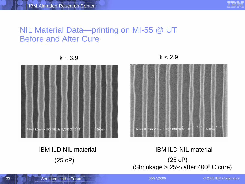
NIL Material Data—printing on MI-55 @ UTBefore and After Cure
IBM ILD NIL material
(25 cP)(Shrinkage > 25% after 4000 C cure)
k < 2.9
IBM ILD NIL material
(25 cP)
k ~ 3.9

IBM Almaden Research Center
© 2003 IBM Corporation23 Sematech Litho Forum 05/24/2006
POSS based Low-k NanoImprinting Materials
Properties
Treatment t (nm) RI Density (g/cm3)
k (250 C)
E Modulus (GPa)
UV/ RT 1075 1.4901 1.348 4.33 6.29+-0.12
UV/RT
400oC / 1h
664 1.4811 1.268 3.05 5.97+-0.10
IBM Almaden Research Center
© 2003 IBM Corporation24 Sematech Litho Forum 05/24/2006
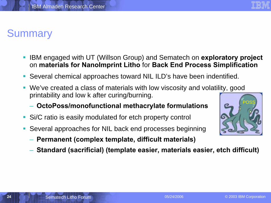
Summary
IBM engaged with UT (Willson Group) and Sematech on exploratory projecton materials for NanoImprint Litho for Back End Process SimplificationSeveral chemical approaches toward NIL ILD’s have been indentified.
We’ve created a class of materials with low viscosity and volatility, good printability and low k after curing/burning.– OctoPoss/monofunctional methacrylate formulationsSi/C ratio is easily modulated for etch property control
Several approaches for NIL back end processes beginning– Permanent (complex template, difficult materials)– Standard (sacrificial) (template easier, materials easier, etch difficult)
POSS
IBM Almaden Research Center
© 2003 IBM Corporation25 Sematech Litho Forum 05/24/2006
Template Materials (e-beam resists)
Desire positive and negative tone materials with the following characteristics for this 1X application– Resolution to support 22nm node
– Low LER
– Relatively fast writing speeds

IBM Almaden Research Center
© 2003 IBM Corporation26 Sematech Litho Forum 05/24/2006
nABLE-An Internally developed negative resist (e-beam) 200 nm pitch/200uC/cm2
Linewidth = 31 nmHeight = 119 nm
IBM Almaden Research Center
© 2003 IBM Corporation27 Sematech Litho Forum 05/24/2006
Conclusions and Recommendations
Template is Achilles Heel– Industry focus on mask technology should be leveraged
– Better Resists for mask/template making (resolution/speed/LER)
Imprint R&D should be enabled by Sematech for 22nm node– Tooling
– Materials Testing