nanosilicon crc press - Главная | ИСТИНА · 2016-06-05 · 3.6. the influence of...
TRANSCRIPT

NanosiliconProperties, Synthesis,
Applications, Methods of Analysis and Control
A. A. Ischenko, G. V. Fetisovand
L. A. Aslanov

Nanosilicon


NanosiliconProperties, Synthesis,
Applications, Methods of Analysis and Control
A. A. IschenkoProfessor and Head of the Department of Analytical Chemistry
Moscow Lomonosov State University of Fine Chemical Technologies
G. V. FetisovProfessor of Chemistry, Moscow Lomonosov State University
L. A. AslanovProfessor and Head of the Laboratory of Structural Chemistry, Moscow

CRC PressTaylor & Francis Group6000 Broken Sound Parkway NW, Suite 300Boca Raton, FL 33487-2742
© 2015 by CISPCRC Press is an imprint of Taylor & Francis Group, an Informa business
No claim to original U.S. Government worksVersion Date: 20140611
International Standard Book Number-13: 978-1-4665-9423-4 (eBook - PDF)
This book contains information obtained from authentic and highly regarded sources. Reasonable efforts have been made to publish reliable data and information, but the author and publisher cannot assume responsibility for the validity of all materials or the consequences of their use. The authors and publishers have attempted to trace the copyright holders of all material reproduced in this publication and apologize to copyright holders if permission to publish in this form has not been obtained. If any copyright material has not been acknowledged please write and let us know so we may rectify in any future reprint.
Except as permitted under U.S. Copyright Law, no part of this book may be reprinted, reproduced, transmitted, or utilized in any form by any electronic, mechanical, or other means, now known or hereafter invented, including photocopying, microfilming, and recording, or in any information stor-age or retrieval system, without written permission from the publishers.
For permission to photocopy or use material electronically from this work, please access www.copy-right.com (http://www.copyright.com/) or contact the Copyright Clearance Center, Inc. (CCC), 222 Rosewood Drive, Danvers, MA 01923, 978-750-8400. CCC is a not-for-profit organization that pro-vides licenses and registration for a variety of users. For organizations that have been granted a pho-tocopy license by the CCC, a separate system of payment has been arranged.
Trademark Notice: Product or corporate names may be trademarks or registered trademarks, and are used only for identification and explanation without intent to infringe.
Visit the Taylor & Francis Web site athttp://www.taylorandfrancis.com
and the CRC Press Web site athttp://www.crcpress.com

vForeword
Contents
Foreword xiii Abbreviations xxiii
Part I
1. Some properties of semiconductors – terminology 11.1. The electrical conductivity of semiconductors from the viewpoint of band theory 3
1.1.1. Direct- and indirect-gap semiconductors 41.2. Quasiparticles in a solid 61.3. The influence of defects on the electronic structure 8
1.3.1. Localized states 91.4. Photoabsorption and luminescence of semiconductors 12
1.4.1. Electroluminescence of semiconductors 151.5. Dimensional constraints and quantum effects 15
1.5.1. Luminescence of indirect-gap semiconductors 221.6. The surface and surface states 26
1.6.1. Reconstruction of the surface 26 Concluding remarks 28 References for Chapter 1 29
2. Structure and properties of silicon 312.1. The structure of crystalline silicon 332.2. The electrical properties of silicon 37
2.2.1. Summary of the basic physical properties of crystalline Si 40
2.3. Crystal lattice defects 43 2.3.1. Extended defects 46 2.3.2. Surface 49
2.4. Amorphous silicon 53 2.4.1. The model of the amorphous state 54 2.4.2. The electronic structure of the amorphous state 57
2.5. Silicon clusters 61 2.5.1. The difference between the clusters and amorphous and
crystalline phases 63 2.5.2. Theoretical studies of the structure and properties of

vi Nanosilicon
clusters 64 2.5.3. Classification of Si clusters 66 2.5.4. Theoretical studies of small clusters of Si 68 2.5.5. Structure and properties of large clusters of Sin 70 2.5.6. Experimental data on the growth kinetics of Si clusters 71
2.6. Silicon nanocrystals 812.7. Quantum size effects in nanosilicon 84
2.7.1. The luminescence of silicon nanoparticles 84 2.7.2. Measurements on a single nanocrystal 90
2.8. Surface chemistry of Si nanoparticles and its effect on the properties 91
2.8.1. Effect of hydrogen passivation of Si nanoparticles 94 2.8.2. Effect of surface oxygen 96 2.8.3. The effect of doping on the electro-optical properties of nc-Si 97 Conclusion 98 References for Chapter 2 101
3. Porous silicon: Luminescence properties 1113.1. Methods of production of porous silicon 1133.2. Main structural characteristics of porous silicon 1193.3. Luminescence of porous silicon 122
3.3.1. Models to explain the origin of the photoluminescence of porous silicon 123
3.4. Quantum-size effect (QSE) 1253.5. Exciton effects in photoluminescence of porous silicon 1293.6. The influence of molecular environment on the luminescent properties of P-Si 131
3.6.1. Effect of active molecules on the luminescence of P-Si 131 3.6.2. Luminescence of porous silicon with embedded dye molecules 138
3.7. Investigation of porous silicon by optical time- resolved spectroscopy 140 References for Chapter 3 144
4. Quantum dots 1514.1. Quantum dots based on nanosilicon 1524.2. Investigation of structural-phase transformations and optical properties of composites based on silicon nanoclusters in the silicon oxide matrix 158
4.2.1. The hypothesis of the percolation nature of the structure of nc-Si/SiOy films 159 4.2.2. Investigation of photoluminescence and electrical properties of nc-Si/SiOy films at optical excitation 1634.3. The long coherence time in quantum dots 1654.4. The dependence of the width of the optical gap
Contents
viiForeword
of silicon quantum dots on their size 1684.5. The characteristics of excitons and exciton photoluminescence of structures with silicon quantum dots 170
4.5.1. The model of a quantum dot and the spectrum of electron–hole excitations 1714.5.2. Calculation of the characteristic time of radiative recombination of electron–hole excitations in the QD 1734.5.3. Excitonic photoluminescence in silicon quantum dots 1764.5.4. Comparison with the experiment 177
4.6. Silicon-based nanowires 1814.7. Silicon quantum dots doped with boron and phosphorus 183 Concluding remarks 187 References for Chapter 4 188
Part II
5. Synthesis, surface modification and characterization of nanosilicon 1945.1. Classification of synthesis methods 1945.2. Physical methods of producing nanosilicon 195
5.2.1. Ion implantation of silicon in SiO2 1965.2.2. Laser ablation of crystalline silicon 2045.2.3. Production of nanosilicon in evaporation of crystalline silicon by a beam of accelerated electrons 2105.2.4. Condensation of silicon vapours 213
5.3. Physico-chemical methods 2145.3.1. Principles of plasma-chemical synthesis methods 2145.3.2. The method of laser-induced dissociation of silane 2455.3.3. Electrochemical etching 255
5.4. Chemical methods of synthesis 266 5.4.1. Nanosilicon produced from silicon monoxide 2665.4.2. Effect of temperature in synthesis of nc-Si from monoxide on the optical properties of nanosilicon 2765.4.3. Recovery of silica with magnesium 2865.4.4. Recovery of silicon dioxide magnesium silicide 2875.4.5. Synthesis of nanosilicon in solution 2895.4.6. Synthesis in supercritical fluids 3005.4.7. Mechanochemical synthesis 3015.4.8. Interaction of precursors in the gas phase 3025.4.9. Silicon nanowires 303
5.5. Passivation of surface and functionalization of nc-Si 3075.5.1. Functionalization of nc-Si in a spray 3095.5.2. Hydrosilylation 3125.5.3. Functionalization of surface by substitutional reactions 319
Contents

viii Nanosilicon
5.5.4. Using the oxidized surface layer 321 Concluding remarks 322 References for Chapter 5 323
6. Thermal oxidation processes in nanosilicon powders 3426.1. Spectral manifestations 3436.2. Paramagnetic centres 3516.3. Effect of carbon impurities on thermal oxidative processes in nanoscale silicon powders 3596.4. Effect of water 367 Concluding remarks 374 References for Chapter 6 376
7. Thin films deposited from sol of silicon particles 3797.1. Synthesis of powders and deposition of films nc-Si 3807.2. Methods of analysis 381
7.2.1. Absorption in UV and visible ranges 383 7.2.2. Raman scattering 386
7.3. Dielectric and transport properties of thin films deposited from sols containing silica nanoparticles 391
7.3.1. Impedance spectra and ellipsometry 393 7.3.2. AC conductivity of nc-Si films 398 7.3.3. The conductivity mechanism 399
Concluding remarks 407 References for Chapter 7 408
Part III
8. Methods for investigating and controlling the structure and properties of nanosilicon 4128.1. Transmission electron microscopy 413
8.1.1. Image modes 415 8.1.2. Studying silicon particles by TEM and HRTEM 421 8.1.3. Transmission electron microscopy with energy loss spectrometry 423 8.1.4. Energy-filtered transmission electron microscopy 425
8.2. Scanning probe microscopy methods 427 8.2.1. Scanning tunnelling microscopy 427 8.2.2. Atomic force microscopy 431
8.3. X ray diffraction analysis of nanopowders 432 8.3.1. Features of X-ray diffraction patterns of nanomaterials 435 8.3.2. Inapplicability of classical XDA to nanomaterials 436 8.3.3. X-ray diffraction analysis of total scattering patterns 439
Contents
ixForeword
8.4. Structural analysis using absorption spectra of X-rays 450 8.4.1. Principles and methods of XAFS analysis 451 8.4.2. Examples of studying nanosilicon by XAFS methods 456 8.4.3. The DAFS method 465
Conclusion 467 References for Chapter 8 468
9. Methods for controlling nanosilicon particle size 4739.1. Methods for determining the size of nanoparticles by dynamic light scattering 476
9.1.1. The method of photon correlation spectroscopy (PCS) 4789.1.2. The method of photon cross-correlation (PCCS) 4919.1.3. Examples of application of PCS and PCCS 4939.1.4. The measuring equipment 495
9.2. Determination of dispersion by Raman spectra 4959.2.1. The distribution function of the size of ns-Si from Raman spectra 499
9.3. Particle size distribution determined by the method of small-angle scattering of X-rays 504
9.3.1. Basic principles of the method of SAXS 5069.3.2. Diffraction patterns of small-angle scattering 5079.3.3. Theoretical basis of microstructure analysis by SAXS 5099.3.4. Analysis of the measurement results 514
References for Chapter 9 514
10. New X-ray diffraction methods for analysis of the structure and morphology of nanocrystalline powders 51910.1. Introduction 51910.2. Theoretical basis of the WPPM method 524
10.2.1. Useful definitions 524 10.2.2. Diffracted intensity: Fourier approach 524
10.3. Broadening components 526 10.3.1. Instrument 526 10.3.2. Domain size and shape 528 10.3.3. Lattice distortions 530 10.3.4. Twin and deformation faults 533 10.3.5. Assembling the equations into a peak and modelling the data 534
10.4. Examples of WPPM Analysis 535 10.4.1. Nanocrystalline ceria 535 10.4.2. Copper oxide 538
10.5. Beyond the WPPM 541 Conclusions 549
Contents
x Nanosilicon
References for Chapter 10 549
11. Methods of femtosecond spectroscopy and time-resolved electron diffraction 55311.1. Femtosecond spectroscopy 555
11.1.1. Experimental procedure 555 11.1.2. The method of femtosecond absorption spectroscopy 556 11.1.3. Photoluminescence properties of silicon quantum dots 559
1.1.2. Surface states as a means to control the photoluminescence of silicon quantum dots 55911.3. Si-QDs with the modified surface and their luminescent properties 56011.4. Ultrafast relaxation dynamics of excitons in silicon quantum dots 56511.5. Methods for studying coherent 4D structural dynamics 572
11.5.1. Ultrafast electron crystallography (UEC) 573 11.5.2. Surfaces and crystals 576 11.5.3. Structural dynamics of the surface 576 11.5.4. Time-resolved electron nanocrystallography (UEnC) 578
11.6. Dynamic transmission electron microscopy 581 Conclusion 583 References for Chapter 11 585
Part IV
12. Fluorescent labels based on silicon 58912.1. Producing nanosilicon for biological applications 590
12.1.1. Surface modification of nanocrystalline silicon by silanization 591 12.1.2. Surface modification of nanocrystalline silicon by hydrosilylation 592
12.2. Applications of nanosilicon in biomedicine and biotechnology 59412.3. Biodegradable porous silicon nanoparticles for in vivo applications 601 Concluding remarks 609 References for Chapter 12 610
13. Porous silicon as a photosensitizer of generation of singlet oxygen 61313.1. Introduction 61313.2. The electronic configuration of the oxygen molecule 61513.3. Photoluminescent diagnosis of singlet oxygen with its generation in porous silicon 617
Contents
xiForeword
13.4. Photosensitization of singlet oxygen in powders of porous silicon and aqueous suspensions 620
13.4.1. Photosensitization of singlet oxygen in the gas phase 620 13.4.2. EPR diagnostics of photosensitization of singlet oxygen 623 13.4.3. Quantitative analysis of the photosensitization of singlet oxygen 62513.4.4. Photosensitization of singlet oxygen in liquids 629
13.5. Biomedical aspects of photosensitized generation of singlet oxygen in porous silicon 632 References for Chapter 13 633
14. Sunscreens 63714.1. Solar radiation and its effect on the skin 63814.2. Using nc-Si as a sunscreen component 64114.3. Modern sunscreens 64414.4. Preparation of specimens of emulsion compositions with nc-Si 647
14.4.1. Measurements of transmission spectra in the UV and visible region 648 14.4.2. Measurement of transmission spectra in the integrating sphere 650 14.4.3. Measurements of the Raman spectra 656
14.5. nc-Si composites with natural biologically active compounds 658 Concluding remarks 659 References for Chapter 14 662
15. Polymer nanocomposites based on nanosilicon 66815.1. Polymeric hydrogels 66915.2. Nanocomposite films with UV-protective properties based on polyethylene 67415.3. Immobilization of luminescent nanosilicon in the matrix of microdispersed polytetrafluoroethylene with supercritical carbon dioxide 682 Concluding remarks 690 References for Chapter 15 69116. Applications of nanosilicon in solar energy 69416.1. Silicon solar cells 69516.2. Improving the efficiency of solar cells with nc-Si 69916.3. Photovoltaic windows 703 References for Chapter 16 705
Index 707
Contents

xii Nanosilicon
xiiiForeword
Foreword
Numerous experimental and theoretical studies show that the transition of particle sizes – the structural elements of matter – to the nanometric range, when the particle contains only a few tens or hundreds of atoms, leads to a qualitative change in the properties of the object. At the same time, the structural elements and material in general (nanomaterial), built on their basis can acquire the physical, physico-chemical and chemical properties differing substantially from the material, which is, for example, a bulk crystal, have identical qualitative composition or a substance constructed from particles of the micron or sub-micron size. On the other hand, the properties of the particles with dimensions of the order of several nanometers (several tens of angstroms) can be also very different from the properties of individual atoms and molecules, their generators. This refers to the nanosized crystals and clusters.
One of the essential, inherent characteristics of the nanocrystal is the distribution function of the particle size. The main parameters of the distribution function of the particle size – the position of the maximum, half-width, asymmetry and excess are essentially manifested in, for example, the optical properties of the nanomaterial and composites based on it. The directional change of these characteristics of the size distribution functions of the silicon nanoparticles leads to the correlated change of their spectral properties. The purposeful change of the particle size distribution function is achieved primarily by modification of the technological conditions for their preparation, fractionation, material, chemical effects in etching and annealing in different environments, monitoring the composition and amount of impurities in the core and the shell of nanocrystalline silicon, nanoparticle surface modification.
A striking example of the effect of the size on the properties of materials is nanocrystalline silicon, which in the form of nanosized objects – films of nanometer thickness – is transparent to visible light, but capable of absorbing ultraviolet light, whereas macroscopic samples of silicon are opaque to visible light. With the change in size the type of conduction of particles can change. For example, changing the diameter and chirality of carbon nanotubes changes the character of the conductivity of a metal to a semiconductor. It is known that gold is diamagnetic. However, direct measurements of spin polarization using the magnetic circular dichroism method at synchrotron radiation show that gold clusters ~ 1.9 nm in size,

xiv Nanosilicon
which contain about 210 atoms exhibit ferromagnetic properties unusual for gold. There are many other such examples, showing changes in the physical and chemical properties of systems with a decrease in their size to the nanometer scale.
The reasons for significant differences in the properties of nanoparticles in comparison with the properties of the bulk material are explained by their having a highly developed specific area surface, as well as quantum effects, manifested by size limitations. These factors can modify properties such as reactivity, strength, electrical and magnetic characteristics. The size constraint of the matter particles by the quantity comparable to the de Broglie wavelength of an electron leads to the situation in which the the quantum effects may dominate its behavior.
Reducing the particle size to a few atomic or molecular diameters leads to a drastic restriction of the range of possible energy states of electrons or excitons (the ‘electron–hole’ pair) in the particles, resulting in pronounced specific electro-optical and magnetic properties of the particles.
The objects in which these effects are pronounced, are quantum dots and quantum wells, which are used in optoelectronics. When the particle size decreases to a few hundred atoms, the density of states in the conduction band – upper zone containing free electrons – changes radically. The continuous density of states in the band is replaced by the discrete levels, the intervals between which may be greater than thermal energy, which leads to the formation of a slit similar to the bandgap in semiconductors. Among the variety of different quantum dots we can defined several main types that are most frequently used in experimental studies and numerous applications. First of all, it is nanocrystals in liquids, glasses, and wide-band dielectric matrices. If they are grown in glass matrices then they generally have spherical form. It is in such a system, in which CuCl quantum dots were embedded in a silicate glass, in which the study of one-photon absorption revealed for the first time the effect of three-dimensional quantum confinement of excitons described by Ekimov and Onuschenko in 1981 (Ekimov A.I., Onuschenko A.A., Quantum size effect in three-dimensional microscopic semiconductors, Pis'ma ZhETF, (1981), vol. 34, No. 6, pp. 363–366). This work marked the beginning of the rapid development of the physics of quasi-zero-dimensional systems.
The nanosized cluster consisting of atoms is somewhat similar to the molecule – the presence of a discrete set of energy levels, types of orbitals electronic transitions between which determine the spectral properties of the nanoparticles. Eventually, it is possible to reduce the cluster size to the level at which its diameter approaches the wavelength of the electron (de Broglie wavelength). In this case, the energy levels can be calculated by considering the quantum problem of elementary particles in a potential well or a limited periodic potential. The advent of new electronic properties of the nanoparticles in comparison with the material of macroscopic dimensions (bulk materials) can also be explained on the basis of the Heisenberg
xvForeword
uncertainty principle: reduction of the region of spatial localization of the electron leads to an increase the range of the values of its momentum and energy. The energy spectrum of the electron will be determined not only by the chemical nature of atoms or molecules forming the particle, but also by the particle size. Interestingly, the quantum size effect is manifested in semiconductors at larger particle sizes than in metals because of the greater de Broglie wavelength of electrons in semiconductors. In semiconductors, the de Broglie wavelength can reach tens of nanometers, while in metals it is ~0.5 nm.
With the particle size decreasing to nanometers silicon exhibits properties unusual for the bulk material, which causes an interest in it, as in an optical material. At the end of 1990 there was a real sensation in the science of semiconductors. Lee Canham, a researcher from the UK, in the article (Canham L.T., Silicon quantum wire array fabrication by electrochemical and chemical dissolution of wafers, Appl. Phys. Lett., 1990. vol. 57, 1046–1048) reported the observation of an effective red-orange photoluminescence of porous silicon at room temperature, which is not characteristic of conventional silicon as the typical representative of indirect-gap semiconductors. This report triggered great interest to researchers around the world. It was shown that the effect observed is due to quantum size constraints of silicon nanostructures. It was established that reducing the size of the Si crystal to several hundred atoms makes it a completely new material with new properties – both electronic or non-electronic, including the ultra-bright and very stable luminescence which could not be observed previously for bulk samples.
Part icular interest to the ul t ra-bright luminescence of s i l icon nanostructures is due to several reasons:
First, it is interesting to know why this effect is negligible in bulk samples of Si, how to make it more prominent in the nanoscale state and whether it is possible to create solid-state lasers based on nanocrystalline silicon?Second, the synthesis of light-emitting nanoparticles can be very cheap and economically attractive for the production of light sources.Third, silicon is available in large quantities and can be a very effective material for microelectronics. Light-emitting silicon nanoparticles could be the basis for a new generation of electronic instruments and extend the functionality of silicon technology from microelectronics to optoelectronics and biophotonics.
The influence of the size effect on the photophysical properties of nanosilicon has been studied intensively and extensively from the beginning of the 90’s of the XX century. The results show the influence of the surface of the silicon nanoparticles on the same properties that are influenced by the dimensional effect. nc-Si particles with a diameter of 2 nm are composed of 280 silicon atoms and 120 of them (43%) are on the surface and at a diameter of 1 nm nc-Si consists of 29 atoms of which only five

xvi Nanosilicon
are inside the nanoparticle. The composition and surface structure of nc-Si strong influence the LUMO energy, and it affects the band gap and optical properties of nc-Si. The ratio of the influence of the size effect and the surface on the optical properties of nc-Si is formulated in general terms as follows: the smaller the size of nc-Si, the larger the surface and the stronger the effect of the surface on the properties of nc-Si. Conversely, the larger the nc-Si, the stronger its effect of the internal atoms on its properties and the model of the size effect works better.
Crystal defects are traps of excitons and they are especially abundant on the surface of nc-Si. The excitons, captured by defects in the crystal structure, are called Frenkel excitons or small radius excitons, since the electron and the hole are located in the neighborhood at a distance of several angströms, i.e. much smaller than the size of the nanoparticle. In bulk silicon the excitons, captured by surface defects, can be both inside the forbidden zone and outside it. In the first case, they manifest themselves optically, in the second case – no. With decreasing particle size of nc-Si the width of the bandgap increases, and the surface states which in crystalline silicon were outside the bandgap fall into it, which changes photoluminescence (PL) spectrum. Thus, the size effect and the surface jointly affect the optical properties of nc-Si.
The rate of radiative recombination of electron-hole pairs localized on the surface is greatly increased compared to the free exciton in the volume of nc-Si, since the distance between the hole and the electron in the localized exciton (Frenkel exciton) is very small, and their wave functions will inevitably overlap. Using PL spectra with a time resolution it has been shown that the decay time of the PL emanating from the surface states is 4.1–4.2 ns, and the high rate of radiative recombination leads to the emission of many photons from one nc-Si, which is very important for practical applications. Usually, nc-Si emits red light from the volume with lifetimes in the microsecond and longer time ranges, and photoluminescence from surface states with lifetimes in the nanosecond range is shifted to the blue region of the spectrum.
Recently, it has been possible to get the PL spectra from single isolated nc-Si. It was found that the overall yield of PL varies considerably from one nc-Si to another. Such changes of quantum efficiency are attributed, in particular, to the effect of unexpected termination of the light emission from the nc-Si, which is caused by the presence of traps of charges on the surface of each particle of nc-Si. These traps can capture one of the charges of the electron–hole pair, making the nc-Si particle charged and, therefore, non-radiative. nc-Si particle returns to the radiative state when the charge carrier is released from the trap. Particles of nc-Si ‘blink’, and each nc-Si particle has its own dark time which depends on the configuration of the traps unique to each particle of nc-Si.
PL depends on the method of synthesis of nc-Si, and also on the surface modification of nc-Si with, for example, silicon dioxide, hydrogen or

xviiForeword
organic groups compounds. Some authors state that oxygen more efficiently modifies the surface of nc-Si than hydrogen and this results in a much greater increase in the luminescence intensity. Besides, it was found that the presence of (Si = O) and (Si–O–Si) groups on the surface of nc-Si results in an impurity level inside the band gap from which the radiative recombination of the exciton can take place. Thus, the luminescence spectrum should show the Stokes shift relative to the photoexcitation wavelength. This result was obtained by the theoretical method of the density functional for nc-Si with a diameter of less than 2 nm. However, the experimental results show that silica particles with a diameter less than 2.15 nm behave themselves as an amorphous substance, and since the properties of the amorphous and crystalline silicon are different, the possible amorphous state of very small silicon particles should be taken into account.
In nanosilicon there is competition between radiative and non-radiative recombination of electron–hole pairs as a result of excitation. One of the channels of non-radiative recombination centers are Pb-centres – single electrons in the dangling bonds of the surface atoms of silicon. Their elimination is one of the main tasks of modifying the surface of nc-Si. The surface of nc-Si to a large extent determines the quantum efficiency of luminescence of nc-Si.
After Canham’s discovery, intensive research started into nanosilicon and the number of publications in the scientific periodical literature has been rapidly increasing from year to year (see the English-language statistics in Fig. F.1).
A large number of scientific publications has also come out in the national languages. For example, the statistics for 2010 show that, if we
Fig. F.1. Number of publications in English devoted to the nanocrystalline silicon and silicon nanoclusters during the 1990–2010 period. Statistics for the period 1990–2008is taken from the book (Pavesi & Turan, 2010) – see the following list of monographs.Statistics for 2009–2010 assembled by the same Internet search method using Google Scholar. Keywords: ‘low-dimensional silicon’ or ‘silicon nanocrystal (s)’ or ‘silicon nanocluster (s)’.
Years
Num
ber
of a
rtic
les
xviii Nanosilicon
take the number of English-language publications (often the results of international studies) as 1, the relative number of publications in the ‘rare’ languages (purely national research) is as follows: 1.64 – Japanese, 0.335 – Chinese, 0.038 – in Russian, 0.024 – Korean.
Published research for nanosilicon is regularly analyzed by international teams of experts and published in collective monographs, especially on the problems of synthesis, characterization, surface modification and application of nanosilicon. Only in English in the last 20 years after the discovery of luminescence in porous silicon more than 10 monographs were published, of which the most complete and well-known are:
Properties of Porous Silicon, Ed. by L. Canham, INSPEC, London, UK., 1997.Nanoparticles and Nanostructured Films: Preparation, Characterization and Applications, Ed. by J.H. Fendler, Wiley-VCH Verlag GmbH, 1998.Light emitting silicon for microphotonics, Ed. by S. Ossicini, L. Pavesi, F. Priolo, Springer-Verlag, 2003.Towards the first silicon laser, Ed. by L. Pavesi, S.V. Gaponenko, L. Dal Negro, Springer, 2003.Silicon: evolution and future of a technology, Ed. by P. Siffert, E. F. Krimmel, Springer, 2004.Silicon Nanoelectronics, Ed. by S. Oda, D. Ferry, Taylor & Francis Group, LLC, 2006.Nanosilicon, Ed. by V. Kumar, Elsevier Ltd., 2007.Silicon nanophotonics: Basic principles, present status and perspectives, Ed. by L. Khriachtchev, World Scientific Publishing Co. Pty. Ltd., 2009.Device applications of silicon nanocrystals and nanostructures, Ed. by Nobuyoshi Koshida, Springer Science-Business Media, LLC, 2009.Silicon nanocrystals: Fundamentals, synthesis and applications, Ed. by L. Pavesi, R. Turan, Wiley-VCH Verlag GmbH & Co. KGaA, Weinheim, 2010.
However, unfortunately, in Russian so far no one book devoted to the systematic exposition of the scientific problems of nanosilicon and the prospects for its practical application. The authors of this monograph tried to fill this gap and present the main achievements in the field of physics and chemistry of nanosilicon. The book describes methods for production nanosilicon, its electronic and optical properties, research methods that allow to characterize the spectral and structural properties of this unique material, and some of its possible applications.
The book consists of 16 chapters, which are divided into four interrelated parts. At the same time, the book is structured so that each chapter can be read as an independent review on the subject indicated by its title. For this reason it was decided to leave the lists of references in each chapter and not constitute a single long list to the entire monograph. In general, the monograph reflects the results of more than 1500 publications.

xixForeword
The first part deals with the basic properties of semiconductors, including causes of the size dependence of these properties, structural and electronic properties and physical characteristics of the various forms of silicon with the theoretical and experimental research results. Examples of porous silicon and the quantum dots are used to analyze the quantum size effects enabling the control of the properties of nanocrystalline silicon. Because the book is intended for a wide audience interested in nanocrystalline silicon, to avoid distracting the reader by referring to the special literature, the beginning of this part contains a chapter that gives a summary of the physics of semiconductors and solid-state theory, which may facilitate the understanding of the subsequent material. Readers who are familiar with these items can skip this chapter.
The second part is central to the monograph and is devoted to the synthesis of nanosilicon, modification of the surface of nanoparticles and the properties of the resulting particles. Much attention is paid to the study of photoluminescence of silicon nanoparticles
The modified nanoparticles obtained to date are soluble in organic solvents and in water. It is shown that the properties of the obtained material depend on the size of the central silicon core and the protective shell. However, only a few studies clearly shows the influence of the shell on the optical properties of nanosilicon. Based on the analysis of the studies presented in this chapter, it is possible to conclude that the numerous results are ambiguous and, in some cases, contradicting. The chemical composition of the surface layer significantly affects the LUMO energy and, respectively, the bandgap value of nc-Si with a diameter less than 5 nm. This helps to understand the mismatch of data across different studies of the photoluminescent properties nanoparticles, which have identical dimensions.
A significant difference between the properties of the material built, for example, from individual the atoms or molecules of the substance having the same composition but comprising nanoparticles is linked not only with the manifestation of the quantum size effect, but also with the absence of the identity of structural elements of the nanomaterial. In contrast to the atoms or molecules, the nanoparticles are not completely identical. Strictly speaking, they differ not only in size but also in composition. It can be assumed that even nanoparticles of the same size are not identical because of possible differences in the quantity, composition and distribution of impurities which each nanoparticle contains. The presence and composition of the impurities are determined by the entire ‘history’ of nanoparticles, depending on the method of synthesis and subsequent location in the environment. Each nanoparticle is a single compound, and we are dealing with a system of particles for which it is possible to determine the function of the size distribution, but the question of the composition of the individual particles remains open. Appropriate methods of analysis of the nanoparticles have not as yet been developed.

xx Nanosilicon
The third part of the book discussed the methods used for the study and controlling the structure and properties of nc-Si. First of all, it is a ‘standard’ set methods – electron microscopy, spectroscopic and diffraction methods with the features of their application to the study of nanoparticles – which is used to determine the characteristics of nanosilicon. In addition, a separate chapter is devoted to the use of femtosecond spectroscopy, ultrafast electron nanocrystallography and dynamic transmission electron microscopy.
In the past two decades has been possible to observe the motion of the nuclei in the time interval corresponding to the period of oscillation of the nuclei. The observed coherent changes in the nuclear subsystem at such intervals of time determined the fundamental shift from the standard kinetics to the dynamics of the phase trajectories – quantum state tomography.
Therefore, despite considerable progress in the study of nc-Si, with traditional methods of analysis and research, we need to develop new methods for studying the structure and dynamics of nanoparticles. These effective methods that can clarify the relationship of the central core and the nc-Si surface layer are femtosecond spectroscopy and time-resolved diffraction techniques. The application of these methods to the study of nano-objects and nanosilicon generally provides new opportunities for studying the behavior of systems in 4D space-time continuum.
The fourth part describes in detail some of the practical applications of nanocrystalline silicon. One of them is the use of nanoparticles as additives–absorbers of UV radiation and in sunscreens.
It is known that the properties of nanomaterials, as artificial objects, integrable in human activity, are significantly different from the natural properties, in an environment where the humanity has survived for thousands of years. Cosmetics manufacturers often ignore this factor, even neglecting the proper observance of the federal regulations of application of nanomaterials. Numerous examples, given in this monograph, show that reducing the particle size of nanoscale objects changes many of the physical and chemical properties, including, e.g., colour, solubility, material strength, electrical conductivity, magnetic properties, mobility (including the environment and the humans), chemical and biological activity.
Increasing the surface area to volume ratio also increases the chemical activity, increasing the speed of processes, which in the case of bulk materials can be very slow. For example, the effect of the oxygen in the air atmosphere on a nanoparticle can lead to the formation of singlet oxygen and other reactive oxygen-containing species (ROS). ROS have been found in the metal oxide nanoparticles of TiO2 and ZnO, carbon nanotubes and fullerenes, and is the active component oxidative stress, inflammation and consequent damage to DNA, proteins and membranes. Furthermore, the action of ROS opens the possibility of formation of a series of reaction channels involving free radicals. In the case of small TiO2 nanoparticles DNA damage was significantly greater than with the large TiO2 particles. Although TiO2 microparticles (~500 nm) can also cause damage to DNA,

xxiForeword
the nanoparticles of medium size (~20 nm) cause complete destruction of the DNA helix at low doses of UV radiation or without its effect.
Because of the potential toxicity of metal nanoparticles, to replace them in sunscreens it is essential to find alternative ingredients for sunscreen materials which are non-toxic and, at the same time, effective in blocking ultraviolet radiation. As shown in a number of works nanosilicon, being a biocompatible and biodegradable material can become one of the most promising materials for use in sunscreens.
The monograph ends with the subject index.Much of the material presented in this monograph includes the results
obtained by the authors or their participation, and leading experts in this field of research were invited to write some chapters that reflect the latest applications and research methods,
This work was supported by RFBR Fund: Grants 11-02-07031-a, 10-02-92000-HHC-a and 11-02-00868-A.
Acknowledgements
One of the authors (A.A. Ischenko) expresses his sincere appreciation to Prof. V.N. Bagratashvili (Institute of Problems of Laser and Information Technologies, Russian Academy of Sciences), Prof. V.R. Flid (Lomonosov Moscow University of Fine Chemical Technology), Corr. Member of the Russian Academy of Sciences, Prof. P.A. Storozenko (State Scientific Research Institute of Chemistry and Technology of Organic Element Compounds, Lomonosov Moscow University of Fine Chemical Technology), Dr. S.G. Dorofeev (Chemistry Department of Moscow State University), Dr. N.N. Kononov (General Physics Institute, Russian Academy of Sciences), Dr. A.A. Ol’khov (Lomonosov Moscow University of Fine Chemical Technology), Dr. V.A. Radtsig (Institute of Chemical Physics, Russian Academy of Sciences), Dr. A.O. Rybaltovsky (Institute of Nuclear Physics, Moscow State University), Dr. V.N. Seminogov (Institute of Problems of Laser and Information Technologies, Russian Academy of Sciences), A.V. Bakhtin (Lomonosov Moscow University of Fine Chemical Technology), G.V. Bulkhova and Ya.A. Ischenko for valuable discussions, comments and invaluable help in writing the monograph.

xxii Nanosilicon

xxiiiForeword
Abbreviations
AES – Auger electron spectroscopy AEY – Auger electron yield – measuring mode of the Auger electron
yield (one of the mode of measurements of XAFS).AFM – atomic force microscopy a-Si – amorphous silicona-Si:H – hydrogenated amorphous siliconBET – Brunauer–Emmett–Teller method for describing the adsorption
of gasesCARS – coherent anti-Stokes Raman scatteringCCD – charge coupled deviceCL – cathodoluminescence (see EL – electroluminescence)CRN – continuous random networkc-Si – crystalline silicon with a particle size >0.1 μmCVD – chemical vapour depositionDAFS – diffraction absorption fine structure – the fine absorption
structure as measured by X-ray diffractionDAS – dimer–adatom–stacking faultDCA – diffusion cluster approximationDCS – dynamic light scattering DFT – density functional theory – the method of calculation of the
electronic structure of many-particle systems in quantum physics and quantum chemistry
DFTEM – dark field transmission electron microscopy DMC – diffusion Monte Carlo methodDMF – N, N-dimethylformamideDMSO – dimethylsulphoxideDOS – density of states – the density of electronic states – the number
of energy levels in the energy range per unit volumeDOX – doxorubicinDSC – differential scanning calorimetryDTEM – dynamical transmission electron microscopyECL – electrochemical luminescenceEDEXAFS – energy dispersive EXAFS spectroscopyEDMR – electric detection of magnetic resonanceEDS – energy dispersive X-ray spectroscopyEELS – electron energy loss spectrometryEFTEM – energy-filtered transmission electron microscopyEL – electroluminescence (see CL)

xxiv Nanosilicon
EMA – effective medium approximationEMF – electromotive forceEPR – electron paramagnetic resonance – electron spin resonance
spectroscopyEXAFS – extended X-ray absorption fine structure FCC – face-centered cubic latticeFFT – fast Fourier transformationFITC – fluorescein isothiocyanate (fluorescent label in biology)FLY – X-ray fluorescence yield mode – mode of measurement of X-ray
fluorescence yield (one of the modes of measurements of XAFS spectra)
FPSN – fluorescent porous silica nanoparticlesFTIR – Fourier transform infrared spectroscopyHCP – hexagonal closed-packed cellHOMO – highest occupied molecular orbitalHRTEM – high-resolution transmission electron microscopyICP MS – inductively coupled plasma mass spectrometryINDO – intermediate neglect of differential overlap IP – imaging plate – photosensitive plate with optical memory (a type
of X-ray detector)IR – infraredITO – solid solution of indium and tin oxides.LACVD – laser-assisted chemical vapour depositionLCEB – the method of linear combination of energy bandsLDPE – low-density polyethyleneLDS – local density of statesLECBD – low-energy cluster beam deposition techniqueLPCVD – vapor deposition of materials at a low pressureLUMO – lowest unoccupied molecular orbitmc–PTFE – polytetrafluoroethylene microparticlesmc-Si – silicon single crystalMEG – multi-exciton generation mechanismMINDO – modified intermediate neglect of differential overlapMINDO3– Modified INDO, version 3MOS – metal–oxide–semiconductor (structure).nc-Si – silicon nanocrystals (particles with dimensions <0.1 μm) or
nanocrystalline siliconNEXAFS – near edge X-ray absorption fine structure – near-edge fine
X-ray structure of the absorption spectrum (the spectrum in the range ±(30–50) eV relative to the excitation energy of the absorption threshold)
NMR – nuclear magnetic resonancen–-Si – doped silicon with electronic conductivityNW – NanoWire – nanowires

xxvForeword
OIHH – organic–inorganic hybrid hydrogels.OTCS – octyltrichlorosilanep+-Si – doped Si with p-type conductivityPC – paramagnetic centerPCCS – photon cross-correlation spectroscopyPCS – photon correlation spectroscopyPDF – pair distance (distribution) function PE – polyethylenePECVD – vapor deposition of materials after they are processed by cold
plasmaPEG – polyethylene glycolPET – photoinduced electronic transitionPL – photoluminescencePLY – photo-luminescence yield – yield of photoluminescence excited
by X-rays (one of the modes of measurements of XAFS).PMR – proton magnetic resonanceP-Si – porous siliconPTFE – polytetrafluoroethylenePVP – polyvinylpyrrolidoneQCE – quantum constraint effectQCSE – Stark effect in quantum constraintsQD – quantum dotQELS – quasi-elastic scattering – PCS with wavelength changeQMC – the quantum Monte Carlo methodQWR – quantum whiskers (nanowhiskers)RBS – Rutherford backscattering spectrometerRDF – radial distribution functionRGB – red, green, blue – an additive colour model of colour synthesis
based on red, green and blueRPDF – reduced pair distribution function – the reduced pair distance
distribution functionRPECVD – remote PECVD – enhanced by indirect CVD plasma (CVD with
a substrate outside the plasma discharge)RS – Raman scatteringRWL – the natural width of the Raman lineSAED – selected area electron diffraction SAXS – small angle X-ray scatteringsccm – cm3 per minute at standard temperature and pressureSC-CO2 – supercritical carbon dioxide
SCF – self consistent fieldSCF – supercritical fluidsSDDF – size distribution density function of sizeSEM – scanning electron microscopySEXAFS – surface EXAFS spectroscopy.STEM – scanning transmission electron microscopy
Abbreviations
xxvi Nanosilicon
STEM–PEELS – method of spectral imaging in a scanning TEM with parallel electron energy-loss spectrometry
STM – scanning tunneling microscopySTS – scanning tunneling spectroscopyTEM – transmission electron microscopyTEY – total electron yield – measurement mode of the total electron yield
in irradiation with X-rays (one of the modes of measurement of XAFS spectra)
TFT – thin film transistorTGA – thermogravimetric analysisTHF – tetrahydrofuranTMOS – tetramethoxysilaneTOAB – tetraoctylammonium bromideTPSC – thin film solar cellTREOS – triethoxysilaneUEC – ultrafast electron crystallographyUEnC – ultrafast electron nano-crystallographyUV – ultravioletVLS – vapor–liquid–solid – ‘vapor–liquid–solid’ growth mechanism’VSS – vapor–solid–solid – ‘vapor–solid–solid’ growth mechanismXAFS – X-ray absorption fine structure – the fine structure of X-ray
absorption spectrumXANES – X-ray absorption near-edge structure – near-edge fine structureXEOL – X-ray excited optical luminescence – (one of the modes of
measurements of XAFS spectra)XPS – X-ray photoelectron spectroscopyXRD – X-ray analysis

1Some Properties of Semiconductors – Terminology
1
Some properties of semiconductors – terminology
As is known from solid state physics (Ashcroft and Mermin, 1979a and 1979b; Davydov, 1976; Kittel, 1978), the solids can be classified according to the nature of electrical conductivity as electrical conductors (usually metals), semiconductors and insulators (dielectrics). Appreciable conductivity is typical of conductors and semiconductors. In terms of the band theory of solids1, semiconductors differ from metals in that their electrons are located in the valence band, separated from free conduction-band by the forbidden band (energy gap), the width of which can range from several tenths of eV to several eV. In conductors (metal) there is no forbidden gap between the valence and conduction bands. Another significant difference between semiconductors and metals is the strong direct dependence of conductivity on temperature, whereas in metals it is the opposite. In addition, the conductivity of semiconductors is strongly dependent on the purity of the material, i.e. the presence of impurities.
Semiconducting properties can be observed in crystalline materials, as well as in disordered systems – solid amorphous materials (glasses) and liquids (Bonch-Bruevich and Kalashnikov, 1977, Seeger, 1977; Yu and Cardona, 2002; Yacobi, 2004). The decisive factor is the nature of chemical bonding between the particles in the short-range order (in the first coordination sphere) and, consequently, the type of lattice in crystalline solids. This fact is confirmed experimentally. For example, semiconductors such as diamond, silicon, germanium under high pressure are converted into metals because the energy gap between the filled valence band and empty conduction band disappears. This is accompanied by the change of the interatomic bonding and crystal structure. The structure of diamond with
1Band theory of solids is a section of quantum mechanics studying the movement and state of electrons in a solid (see, for instance, Anselm, 1978; Ashcroft and Mermin, 1979; Bonch-Bruevich and Kalashnikov, 1977, Kaxiras, 2003; Moliton, 2009).
Part I

2 Nanosilicon
tetrahedral coordination2 of the interatomic bonds changes to the structure of metallic tin with a higher coordination number. The covalent bond, which can be represented in the form of electronic bridges connecting the atoms in the diamond structure, becomes metallic, non-directional.
There are semiconductors with any type of chemical bond (covalent, covalent–metallic, covalent–ionic) with the exception of pure metallic and purely ionic, and the covalent component of the bond in semiconductors is usually dominant.
The conductivi ty of semiconductors is s t rongly dependent on temperature. An intrinsic semiconductor (or a semiconductor of type i, i.e. ultrapure single crystal semiconductor without impurities and free from defects of the crystal lattice) at the absolute zero temperature has no free carriers in the conduction band, in contrast to conductors, and behaves as an insulator. The permissible content of impurities at which a semiconductor can be regarded intrinsic (i.e. semiconductor of type i), depends on the forbidden band gap of the material. Thus, to achieve the level of intrinsic conductivity at room temperature, the permissible content of impurit ies in Ge should be <5 ·10–9%, while in sil icon <5·10–11%.
Semiconductors differ from metals by a number of properties:1) the electric current in semiconductors, in contrast to metals, is formed
by two types of charge carriers – negatively charged electrons e– and positively charged holes e+;
2) the electrical conductivity of semiconductors is greatly lower than that of metals;
3) the electrical conductivity of semiconductors increases rapidly with increasing temperature, and, as a rule, in a wide temperature range increases exponentially, while in the metals it is reduced and is usually much less dependent on temperature;
4) the electrical conductivity of semiconductors very strongly depends on their purity (the impurity concentration) and usually grows with the introduction of impurities, whereas in the metal the dependence of electrical conductivity on the impurity content is weak and usually of the opposite sign (i.e. most often the introduction of impurities decreases the electrical conductivity of a metal);
5) The electrical conductivity of semiconductors affects exposure to light or ionizing radiation – for metals, this effect is virtually absent or very weak.
Interestingly, these properties of semiconductors are completely similar to the corresponding properties of insulators. The reason for this similarity is an equivalence of the electronic structures of atoms, semiconductors and
2The short-range order of the distribution of the atoms is quantitatively characterised by the coordination number – the number of the nearest neighbours of the atoms, and in the diamond lattice it is equal to 4, i.e. the atoms in the diamond lattice are characterised by tetrahedral coordination.

3Some Properties of Semiconductors – Terminology
insulators, which are different from the electronic structures of metal atoms. For this similarity the semiconductors are sometimes referred to as semi-insulators. The features of the electrical conductivity of semiconductors, metals and insulators can be clearly explained and quantitatively described in terms of the band theory of solids (see, for example, Anselm, 1978, Ashcroft and Mermin, 1979, Bonch-Bruevich and Kalashnikov, 1977, Kaxiras, 2003; Moliton, 2009).
The main factors determining the fundamental properties of the semiconductors (e.g. optical and electrical) are associated with the chemical composition and crystallographic structure, the presence of various defects and impurities (both accidental and intentionally introduced), as well as with the size of a semiconductor or semiconductor structure. The chemical composition and crystal structure define the structure of electron bands (e.g. width and type of band gap and effective mass of charge carriers), which have a major impact on the semiconductor properties. The presence of various defects and impurities is expressed in the addition of various electronic states (both shallow and deep) in the band gap, which greatly alter the optical and electrical properties. Finally, as shown in sections 1.4 and 2.7, as well as in Chapters 4 and 11, the semiconductor properties may be strongly influenced by the effect of quantum-dimensional constraint when the size of the semiconductor becomes comparable with the de Broglie wavelength (in silicon this is usually observed with sizes less than ~10 nm).
1.1. The electrical conductivity of semiconductors from the viewpoint of band theory
Free electrons can have any energy – their energy spectrum is continuous. The electrons, belonging to isolated atoms, have certain discrete values of energy. In a solid, electrons are not only bonded with the atoms, but are also in a potential field of neighbouring atoms, so their energy spectrum is substantially different, it consists of some of the allowed bands separated by bands of forbidden energies.
Electrons in an atom are located at different orbital levels characterized by different distances from the nucleus and, accordingly, a different binding energy of the electron with the nucleus. In the formation of the crystal lattice of the solid the electron orbits are somewhat deformed, and, accordingly, the energy levels of electrons in them are shifted. This shift can be imagined in two ways. On the one hand, we can see that in a solid, an electron can not be subjected to electrical interference on the part of neighbouring atoms – it is attracted to their nuclei and is repelled by electrons. On the other hand, two electrons, by virtue of the Pauli exclusion principle3, can not be on the same orbit in the same energy state. Therefore, 3The Pauli principle can be formulated as follows: the given quantum system in the given quantum state can contain only one particle, and the state of the other particle must differ by at least one quantum number.

4 Nanosilicon
in the formation of a solid body and in the crystallization of atoms into a rigid structure each energy electronic level in the atoms splits into a number of close sublevels combined into an energy band or zone. All the electrons in this energy band have very similar energies. At the orbits close to the nucleus the electrons are in a bound state: they are unable to break away from the nucleus, because although in theory the electron hopping from one atom to another – on the same orbit with respect to energy – is possible, all the lower orbits of the neighbouring atoms are occupied, and the actual migration of electrons between them is not possible.
The most important feature from the viewpoint of electrical conductivity is the valence band – the outer layer of the electron shells of atoms blurred and divided into sub-levels, which in the majority of substances is not filled (the exception – the inert gases, but they crystallize only at temperatures close to absolute zero). Since the outer layer is not saturated with electrons, it always contains free sub-levels, which can take electrons from the outer shell of neighbouring atoms. And the electrons, in fact, migrate within the valence band, and in the presence of an external electrical potential difference they collectively move in one direction, creating an electric current. That is why the region with lower binding energy in which there are freely moving electrons is called the conduction band.
The multiband theory of the structure of the solid can be used to explain the electrical conductivity of the substance. If the valence band of the solid is filled, and the next unfilled energy band is far away, the likelihood that electron transfers to it is close to zero. This means that the electrons are strongly bound to atoms, do not form a conductive layer, and can not leave their place, even under the influence of an external potential difference. This state is typical for insulators – substances that do not conduct electric current.
1.1.1. Direct- and indirect-gap semiconductors
A very important characteristic for the classification of semiconductors is their response to photon radiation. Absorption of light by semiconductors may lead to photon excitation of electrons in a semiconductor so that they pass from one level of the band to another, or rather from the valence band to the conduction band. However, the due to the Pauli exclusion principle, the electrons can move only from the filled energy level into an empty one. In an intrinsic semiconductor (i.e. in the semiconductor, free from impurities and extended defects), all states of the valence band are filled and all states of the conduction band are free, so transitions are possible only from the valence band to the conduction band. To implement such a transition, the electron must receive from the light energy not lower than the band gap width. A photon with lower energy does not cause transitions between electronic states of the semiconductor, so that the semiconductor is transparent to such photons. Transparency is observed for the photons
5Some Properties of Semiconductors – Terminology
Eg/ , where Eg (energy gap) is the band gap width of the semiconductor, is Planck’s constant. This cut-off frequency Eg/ determines the fundamental absorption edge of a semiconductor. For semiconductors which are often used in electronics (silicon, germanium, gallium arsenide), the fundamental absorption edge lies in the infrared range.
Additional constraints on the absorption of light by a semiconductor are imposed by quantum selection rules, in particular the law of conservation of momentum. The law of conservation of momentum requires that the quasi-momentum4 of the final state be different from the quasi-momentum of the initial state by the amount of the absorbed photon momentum. The
of the vector of the reciprocal lattice of the semiconductor, or, equivalently, the wavelength of a photon in the visible region is much larger than the characteristic atomic spacing in the semiconductor. As a consequence, the requirement of momentum conservation is to ensure that the quasi-momentum of the final state in the electronic transition should be almost equal to the quasi-momentum of the initial state. However, this condition at frequencies close to the fundamental absorption edge can be satisfied not for all semiconductors. The point is that there are direct-gap and indirect-gap semiconductors, and this condition is satisfied only for the former. The scheme of the dependence of the energy of current carriers on the quasi-momentum for the direct- and indirect-gap semiconductors is shown in Fig. 1.1.
Optical transitions in semiconductors, in which the electron momentum is almost constant, are called direct or vertical. However, the momentum of the final state may differ significantly from the momentum of the initial state, if in the process of absorption of a photon another, third particle, for example, a phonon, is involved. Such transitions are also possible, although less likely. They are called indirect transitions.
Direct-gap semiconductors such as gallium arsenide, are beginning to strongly absorb light when the light quantum energy exceeds the band gap. In the transition of an electron from the valence to the conduction band free charge carriers form in the semiconductor and hence photoconductivity. Upon return of the semiconductor excited by photons to a stable initial state reverse transitions of the electrons occur from the conduction band to the valence band, accompanied by the emission of a photon. These
4The quasi-momentum is a vector quantity characterising the state of the quasi-particle. The quasi-particle differs from a free particle by the fact that it is subjected to the effect (excitation) from a system in which it is located. The ‘free’ electron, situated in the solid with a variable potential, is a quasi-particle in this sense since it moves in the periodic field of the crystal lattice. In addition, the quasi-free electron (quasi-electron) has the effective mass m* which can greatly differ from the mass of the actual free electron. This also applies to other quasi-particles.

6 Nanosilicon
semiconductors have effective photoluminescence and can be used in optoelectronics.
Indirect-gap semiconductors such as silicon, absorb in the light frequency range with the quantum energy slightly larger than the width of the band gap far less efficiently and only due to indirect transitions. The absorption intensity in such a case depends on the presence of photons and hence on temperature. If the indirect transition a photon is absorbed at the same time as a quantum of light, the energy of the absorbed light quantum may be less by the value of the phonon energy, which leads to absorption at frequencies slightly lower in energy than the energy of the fundamental absorption edge. The cutoff frequency of direct transitions of silicon (EgD in Fig. 1.1b) is greater than 3 eV, i.e. it lies in the ultraviolet spectral region.
1.2. Quasi-particles in a solid
To describe the properties of solids we use such an important concept as ‘collective disturbance of the system’, in which a number of quasi-particles is introduced (see, for example, Brandt and Kul’bachinskii, 2010, Ashcroft and Mermin, 1979a,b; Kaxiras, 2003). In contrast to particles such as bosons, they are not similar to the particles that make up the real systems, and represent the collective (i.e. coherent) motion of many physical particles. Below is a list of quasi-particles and collective excitations, which are often used to describe the physics of solids, in the order of importance when considering the use of the basic material of this monograph.
Fig. 1.1. The positions of the energy maximum in the valence band Ev and of the energy minimum Ec in the conduction band compared to the electron momentum p for photoexcited transition of the electron through the forbidden zone: a – for the direct-gap semiconductor, b – for the indirect-gap semiconductor (scheme for a single crystal of pure silicon), where EgD is the width of the energy gap between the bands in direct and Eg0 – in indirect transition.
a b
7Some Properties of Semiconductors – Terminology
1. Quasi-electron: a quasiparticle consisting of a real electron and an exchange-correlation hole, forming a cloud of the effective charge of opposite sign due to exchange and correlation effects arising from the interaction of all electrons in the system. If the electron is in a periodic potential, its motion is considered as the motion of the quasi-particles. The concept of the quasi-electron was introduced by L.D. Landau. The quasi-electron is a fermion with spin 1/2. Its Fermi energy (the highest occupied state) is about 5 eV and the Fermi velocity (vF = F/me) about 108 cm/sec, i.e. belongs to the category of non-relativistic particles. The effective mass of the quasi-particles can significantly differ from the free electron mass.
2. Hole: a quasi-particle as a quasi-electron, but with a positive charge The hole corresponds to the absence of an electron in the single-particle state below the Fermi level. The concept of the hole is especially useful when the initial state is formed by the states of quasi-particles, which are fully occupied and separated by the energy gap from the unoccupied states. The concept of the hole is introduced in the band theory to describe the electronic effects in the valence band incompletely filled with electrons.
3. Exciton: a hydrogen-like quasi-particle, which is the electronic excitation in a dielectric or semiconductor, migrating through the crystal and not associated with the transfer of electric charge and mass. This is a collective excitation corresponding to the bound states of the conduction electron and the hole. There are two types of excitons: Frenkel excitons and Vanier–Mott excitons. If the electron and hole are located in the same lattice site, i.e. the exciton radius (the distance between the electron and the hole) is a* < a, where a is the crystal lattice spacing, the quasi-particle is called a Frenkel exciton. But such states are usually observed only in molecular crystals, which are also described by Frenkel excitons. If the exciton radius is much greater than the atomic spacing in the crystal, i.e. a* a, then the quasi-particle is called the Vanier–Mott exciton. This type of exciton is typical for semiconductors, where the high dielectric constant leads to a weakening of the electrostatic attraction between the electron and the hole, with the result that it leads to a large electron radius. The binding energy of the electron–hole pair is proportional to e2 a*),
value varies around 10), a* is the distance between two particles forming the exciton (which is usually several lattice spacings and is measured in tens of angstroms), resulting in an energy of ~0.1 eV, or a few tenths of eV. The Vanier–Mott exciton binding energy is generally 0.02–0.005 eV in semiconductors and equals 0.014–0.015 eV in particular for a silicon crystal (Kaxiras, 2003; Yacobi, 2004). For example, for a silicon crystal at a temperature of 1.7 K, this energy is ~0.74 eV.
4. Phonon: a quasi-particle, which is a quantum of vibrational motion of the atoms in the crystal. The concept of the phonon was introduced by I.E. Tamm to describe the collective excitation corresponding to the coherent

8 Nanosilicon
oscillation of the thermal atoms of a solid. The phonon energy is of the order of
5. Polaron: a component quasi-particle (conductance electron + associated phonons), which can move through the crystal as an entity. The concept of the polaron is introduced to describe the polarization in the crystals, which occurs when a negatively charged electron, moving through a lattice of positively or negatively charged ions, causes perturbation of the ions around itself and distorts the crystal lattice. Since the electron motion in this case is associated with the displacement of the ions, the effective mass of the polaron is much greater than the free electron mass.
6. Plasmon: a quasi-particle corresponding to the quantization of the collective oscillations of the gas of free electrons relative to ions in the crystal. The presence of plasmons and of the collective states in the system described by them manifests itself in the long-range Coulomb interactions and is optically observed as the passage or reflection of light. The light
conduction electrons screen the electric field in the light electromagnetic wave, which is most pronounced in metals. The light with a frequency higher than the plasma frequency passes through the solid, because the electrons can not respond quickly enough to screen it; this is mostly characteristic of semiconductors and insulators. The role of the plasmons is particularly great in describing the optical properties of metals and doped semiconductors, and hence also of the transformations between metallic and semiconductor states of the solid, such as in the transition to the size of the particles, creating quantum size limitations. The plasmon energy is defined as � ∼ω π� 4 2ne / me , where n is the number of charged particles per unit volume, and can be measured either by experiments or on the basis of energy losses of the electrons passing through the sample as the energy of the formation of plasmons, or when analyzing the spectrum of light radiation emitted by plasmons. For solids with the usual electron density the plasmon energy lies in the range from 5 eV to 20 eV. In most metals the plasma frequency is in the ultraviolet spectral region, making them shiny when viewed in visible light. In doped semiconductors, the plasma frequency is usually in the infrared region.
There are other quasi-particles used to characterize the properties of solids in condensed matter physics, but they are not as relevant for further understanding of the material of this book, but interested readers can find a detailed discussion of this subject, for example, in Brandt and Kul’bachinskii (2010).
1.3. The influence of defects on the electronic structure
Many of the major defects are electrically active (Yu and Cardona, 2002). Defects that can create free electrons in a crystal are called donors and defects which create a hole (i.e. destroying the free electrons) are called
9Some Properties of Semiconductors – Terminology
acceptors. Examples of defects-donors in Si are the substitutional atoms from the group V, such as P, As and Sb, or monovalent interstitial atoms such as Li and Na. The atoms of group V have one valence electron more than the Si atoms they replaced. In addition, the excess electron is weakly bound to an atom of group V in Si and can be easily excited into the conduction band of the Si crystal. Substitutional atoms from group VI, for example, S, Se and Te in Si, can give two electrons to the conduction band, so they are called double donors. Examples of acceptors in Si are the substitutional atoms of group III, such as B, AI, Ga and In. The substitutional atoms of Group II in Si (e.g. Be, and Zn) are double acceptors. If an impurity substitutional atom has the same valence as the host crystal atom, it is an isoelectronic or isovalent centre.
In the literature, one often finds the terms ‘deep centre’ and ‘shallow centre’ which can be interpreted as some defects with electronic levels located respectively near the middle of the band gap or near the allowed bands.
It is difficult to predict in advance whether a specific impurity atom will be a deep or shallow centre. This can be helped by the following symptoms, which, however are not absolutely immutable.
If the ‘skeleton’ of the impurity atom (the atom minus the outer valence electrons) is similar to the skeleton of its own atom (they can vary by a single nuclear charge), the impurity levels tend to be shallow. If an impurity atom creates a highly localized potential, the most likely result will be the emergence of a deep centre.
The defects are the centres of electron localization. As these electrons and holes are fixed, they are said to be linked. In contrast, electrons in the conduction band and the hole in the valence band of a semiconductor can carry electrical current. That is why they are called free carriers.
In some cases, the defect can produce both shallow and deep bound states. For example, electrons with the envelope wave functions with s-symmetry act as deep centres more frequently than the electrons from the envelope wave functions having p-symmetry.
1.3.1. Localized states
The most important point defects of the crystal structure of semiconductors are chemical impurities, vacant lattice sites (vacancies) and atoms embedded in the interstitials. A common feature for them is the ability to bind and release electrons (Madelung, 1985).
In terms of the influence of point defects on the band model, it turns out that delocalized band states and localized states, associated with defects, can be treated together in one scheme of the energy bands.
In describing the properties of crystalline solids we generally consider two systems: the electrons and the crystal lattice in which there are electrons. These two systems naturally interact with each other. The

10 Nanosilicon
properties of electrons in a potential field of the crystal lattice, i.e. ‘quasi-electrons’, are described by the band model, while the properties of the lattice vibrations are described by the phonon spectrum. Originally the band theory assumes a strict periodicity of the structure of the lattice, which is actually violated by defects. Around some lattice defects some of the delocalized phonon states become localized and decoupled from the continuous spectrum in the form of branches (localized lattice vibrations), resulting in an additional potential around the defect and the reasons for the localization of electronic states. Taken together, this affects the optical properties of solids and the characteristics of the transfer in them.
To understand the influence of defects on the electronic structure of solids one can solve the Schrödinger equation (1.3) for electrons moving in a periodic lattice by adding to it the additional potential introduced by the defect. Examples of this type of analysis can be found in most textbooks on solid state and semiconductor physics (see, e.g. Madelung, 1985).
At large distances of the conduction electron (quasi-electron) from the positive charge, generated by atomic ions, the crystal lattice screens the
In this case, the perturbing potential of the lattice defect is reduced to the potential of the hydrogen atom in a dielectric medium, i.e. in a continuum approximation, the problem of electron motion in the crystal lattice with a point defect is reduced to the well-known and long solved problem of solid state physics.
To limit the number of Bloch functions in the wave packet which participates in the solved equations, we can use the following approximation, in which we only consider the Bloch functions of the conduction band. This can be done if the energy with which the electron is bound in the defect is small compared with the binding energy of the valence electron in the lattice (the width of the energy gap Eg). This approximation corresponds to the defects which are called shallow impurities and allows us to work within the approximate theory of effective mass m*. This condition is satisfied for the majority of donors and point defects in the crystal lattice. Otherwise (deep impurities) the approximation of effective mass m* is inapplicable, and the solution should also take into account the Bloch functions of the valence band. Defects with the properties of the deep impurity whose binding energy is comparable to Eg, act as traps and centres of recombination. The binding energies of the most important donors in Si is less than 1% of the band gap, so they can be considered as shallow impurities (Madelung, 1985).
The results of solving the problem for an electron with effective mass m*
the bound states form a hydrogen-like spectrum, the lines of which (donor levels) lie under the lower edge of the minimum of the conduction band. The Bohr radius of the orbit of the ground state is increased as compared
m/m*) times. For silicon this leads to the value of the Bohr radius in the range from 20 to 50 Å.

11Some Properties of Semiconductors – Terminology
Isolated defects modify not only modify the electronic states in the band model, but also the states in the vibrational spectrum of the crystal lattice. Here, as in the case of the electronic states, the influence of defects has only a small effect on the branches of the phonon spectrum, but in lattices with a basis (as in silicon, having a lattice with basis 2) leads to the appearance of localized states between acoustic and optical branches and above optical branches, and also creates conditions for the possibility of resonant states inside the branches (Madelung, 1985). Localized states are often active in the infrared range and can be found in the absorption spectrum of the crystal.
To describe the properties of solids within the framework of the band theory we use the concept of energy bands, the collective of electrons in the conduction band and collectives of holes in the valence band. To account for the real solid structures, we add to these concepts all the charged and uncharged defects of the crystal lattice, which are considered as separate groups. And all of these collective (each with its own chemical potential) are considered in the interaction, i.e. in reactions with each other. In this description, for example, the relaxation of the excited electron from the conduction band to the donor level means the reaction of the free electron with a positively charged donor atom with the formation of a neutral donor atom. In general, the interaction of the collectives is described similar to the kinetics of chemical reactions using the equality to zero of the total potential of the system in equilibrium and the law of acting masses, which describes the balance between the different collectives.
Of all the collectives of the considered defects two types of lattice defects – vacancies and interstitial defects – are fundamentally different from the impurity atoms. The difference is that the impurity atoms in the ideal case can be completely removed from the crystal, while the vacancies and interstitial defects are thermodynamically unavoidable.
In the conventional model of a semiconductor the photon absorption process implies the formation of electron–hole pairs, with the hole remaining in the valence band and the electron appearing in the conduction band. Accordingly, the reverse process is called the recombination of electron–hole pairs. For interband recombination, the electron returns to the valence band, again emitting a photon, and annihilate with the hole (radiative recombination, photoluminescence). However, radiationless recombination is also possible; in this case the electron returns to the valence band, giving the recombination energy to another electron (Auger recombination) or crystalline lattice by multiphonon processes.
In any recombination process the conservation laws of energy and momentum must be satisfied. Together with the probability of transition, these laws define the lifetime of the excited electron–hole pairs. The transition probability can be significantly higher if the recombination occurs via a two-step process through a defect in the crystal structure (recombination centre). In this case, the electron is first captured by the

12 Nanosilicon
defect, and then released into the valence band. In order to implement this mechanism, the recombination centres should have sufficiently large effective cross sections for interaction with both the conduction and the valence band.
If we consider the kinetics of recombination processes generated by the external excitation of electrons, aloof from radiative or nonradiative transition, without the defects the only possible transitions are the transition of electrons from the electron–hole pair in the steady state depends on the magnitude of excess
n electrons, which in the case of small deviations from n = G G is the number
of electron–hole pairs generated by the external force per unit time.However, remember that along with the absorption-excited electron–
hole pairs in the crystal there are always electron–hole pairs generated by thermal excitation, which constantly appear and recombine, but retained their equilibrium concentration.
1.4. Photoabsorption and luminescence of semiconductors
The peculiarity of the electronic structure of semiconductors is expressed in their specific response to photon radiation and excitation of the electron energy levels (Harrison, 1983; Yu and Cardona, 2002). This is due to the ability of many semiconductor for luminescence.
Luminescence is a glow of a substance that occurs after the absorption of excitation energy by the substance. Following the canonical definition luminescence will mean the excess over the thermal radiation from the body if this excessive radiation has a finite duration (order of 10–10 seconds or more), far exceeding the period of light fluctuations. The concept of duration in this definition was introduced by Russian scientist S. Vavilov5. The duration criterion makes it possible to separate the luminescence from other types of non-thermal radiation: scattering and reflection of light, Raman scattering, bremsstrahlung radiation and Cherenkov radiation. Their duration is less than the oscillation period the light wave (i.e. <10–10 s).
An important feature of the luminescence is that it can occur at much lower temperatures than thermal radiation, since it does not use the thermal energy of the radiating system. Therefore, luminescence is often called ‘cold light’. The physical nature of luminescence is the radiative transitions of electrons from the excited to ground state. In this case the cause of the initial excitation of the system can be represented by a variety of factors: external radiation, chemical reactions, etc.
For a substance to be able to luminesce, its spectra should be of discrete nature, i.e. its energy levels must be separated by zones of forbidden energies. This is just typical for semiconductors. At the same time, metals in solid and liquid states, which have a continuous energy range, do not give 5http://www.femto.com.ua/articles/part_1/2015.html
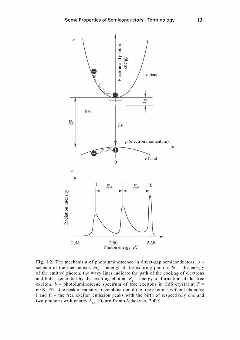
13Some Properties of Semiconductors – Terminology
Fig. 1.2. The mechanism of photoluminescence in direct-gap semiconductors. a – scheme of the mechanism: hv0 – energy of the exciting photon; hv – the energy of the emitted photon, the wavy lines indicate the path of the cooling of electrons and holes generated by the exciting photon; E1 – energy of formation of the free exciton. b – photoluminescene spectrum of free excitons in CdS crystal at T = 60 K: FE – the peak of radiative recombination of the free excitons without phonons; I and II – the free exciton emission peaks with the birth of respectively one and two phonons with energy Eph. Figure from (Aghekyan, 2000).
Elec
tron
and
phot
on
ener
gy
Rad
iatio
n in
tens
ity
c-band
v-band
Photon energy, eV
p (electron momentum)
FE
a
b

14 Nanosilicon
luminescence. The excitation energy in metals is converted in a continuous way into heat, and metals can under X-ray fluorescence only in the short-range, i.e. under the influence of X-rays or electrons of sufficiently high energy to emit X-rays (characteristic X-rays).
For the excitation of luminescence the material must receive the energy exciting the electronic levels in its electronic structure. Depending on the form in which energy is supplied to the luminescent body (luminophor) we distinguish photo-, cathode-, X-ray-, electroluminescence, and so forth.
Photoexcitation of the semiconductor by the absorbed photon prior to emission of fluorescent radiation (the process of photogeneration) can be clearly explained by the diagram in Fig. 1.2, which shows the case of the direct-gap semiconductor.
In this scheme, the transition of an electron from the filled valence band (v-band) to the empty conduction band (c-band) in the absorption of a photon crystal is represented by a vertical arrow, because the transition takes place with virtually no change in momentum, because the momentum of the photon pphbands on the scale of p (i.e. as regards the modulus, the momentum of a light photon is much smaller than the length of the reciprocal lattice vector). If the energy extrema of both bands are located at one value of p (usually p = 0), the direct-gap semiconductor is called direct-gap, if at different p – it is an indirect-gap semiconductor. After absorption of a photon with energy hv0 > Eg the electron with momentum pc appears in the c-band and a hole with momentum pv forms in the v-band (i.e. photogeneration of free charge carriers takes place). The conservation laws of energy and momentum are satisifed in the process of light absorption, so that
p p pv c+ = ph 0. (1.1)
The free charge carriers, generated in absorption of a photon, naturally try to lower their energy to zero. But this opportunity in the separated bands separated is limited – for the hole by the maximum energy of the valence band, for the electron by the minimum of the conduction band. Therefore, the electron drops to the bottom of the c-band, and the holes floats to the ceiling of the v-band, and as a result in direct-gap semiconductors we have an electron and a hole with momenta close to zero. The excess energy released by this relaxation or cooling of the generated charge carriers is used to enhance the thermal vibrations of the crystal lattice, or in other words, leads to an increase in the number of thermal particles – phonons.
The luminous radiation itself is emitted in the process following excitation – recombination. As a result of recombination the electron returns to the valence band (and thus the hole also disappears) and the crystal will be in the original state. The transition of a conduction electron to the vacant site in the valence band (the annihilation of the electrons and the
Eg/h. Such transitions in the emission and absorption spectra correspond to the

15Some Properties of Semiconductors – Terminology
broad (and relatively weak in intensity) bands. Thus, the photoluminescence spectrum of semiconductors is determined by the radiative recombination of non-equilibrium electrons and holes produced by the light.
1.4.1. Electroluminescence of semiconductors
In addition to photoluminescence, electroluminescence also occurs in semiconductors. In 1923, O.V. Losev (see Novikov, 2004) observed the glow of silicon carbide crystals when voltage was directly applied to them, and in 1936 G. Destriau reported the glow of fine crystalline zinc sulphide activated with copper (ZnS:Cu), stirred in a dielectric liquid and placed between the plates of a condenser to which alternating voltage was applied.
This means that in the case of semiconductors luminescence can be excited not only by electromagnetic radiation (photoluminescence), but also by the supply of electricity to the semiconductor (electroluminescence). The strong electric field, close to the breakdown value, can excite semiconductor crystals both due to tunnelling of electrons from the valence band and the luminescence centres the conduction band, and through the acceleration of electrons in the electric field to energies sufficient to ionise the crystal lattice and luminescence centres (impact ionization). In addition, there can be shock-excitation of the luminescence centres. The recombination of electrons and holes, both directly and through the centres of luminescence, as well as a return to the initial state of the excited luminescence centres, lead to the emission of luminescence light. This luminescence is called prebreakdown electroluminescence.
The electric field can also lead to electroluminescence (EL) by another mechanism. The point is that inorganic luminophors are wide- gap semiconductors with impurity conductivity. If they are in direct contact with the electrodes, then the current flow may inject into them additional minority charge carriers. The radiation produced by recombination of these carried with the main carriers, is the luminescence commonly called injection electroluminescence in the literature. This luminescence is observed, for example, the p–n transitions activated in the forward direction. This species of electroluminescence is important for light-emitting diodes.
1.5. Dimensional constraints and quantum effects
The features of the electronic properties that are manifested when the size of the particles approached nanometer range are explained in a simple and accessible way in, for example, review articles (Borisenko, 1997; Belyavsky, 1997; Demikhovskii, 1997, Schick, 1997). To learn more about the effects of quantum dimensional constraints in semiconductors, the reader should refer to, for example, textbooks (Yu and Cardona, 2002; Yu and Cardona, 2010; Hamaguchi, 2010). The consequences of the quantum-dimensional constraints will often be discussed in connection with nanosilicon in

16 Nanosilicon
subsequent chapters of this monograph. Here we consider only the physical essence of this phenomenon.
From the standpoint of quantum mechanics, an electron can be represented by a wave, described by the corresponding wave function (see, for example, Anselm, 1978, Ashcroft and Mermin, 1979, Bonch-Bruevich and Kalashnikov, 1977, Yu and Cardona, 2002, as well as many other textbooks on solid state physics, including physics of semiconductors). The distribution of this wave in nanoscale solid-state structures is controlled by effects associated with the quantum constraint, the interference and the possibility of tunnelling through potential barriers.
A wave corresponding to the free electron in a solid can be easily extended in any direction. The situation changes dramatically when an electron enters the solid state structure, whose size L, at least in one direction, is limited and its size is comparable to the wavelength of the electron. A classical analogue of such a structure is a string with fixed ends. Vibrations of the string can occur only in the mode of standing waves with
n = 2L/n, n = 1, 2, 3,... . Similar patterns of the behaviour are also characteristic of a free electron in the solid state structure of a limited size or an area of a solid bounded by impenetrable potential barriers.
In Fig. 1.3 this situation is illustrated by the example of a quantum string, which has limited sizes of the cross section a and b. Only with the length divisible by the geometric dimensions can propagate in the directions a and b. The allowed values of the wave vector in one direction are given by n = n L (n = 1, 2, 3, ...), where L as shown in Fig. 1.3 can make values equal to a or b. For the corresponding electrons, this means that they can have only certain fixed values of energy, i.e. an additional quantization of energy levels takes place. This phenomenon is called the quantum constraint. In this case, the motion of electrons across the string is restricted and allowed for electrons with a certain energy state, and electrons with any energy can move along the string.
Locking the electron with effective mass m*, at least in one of the directions, in accordance with the principle of uncertainty leads to an
Fig. 1.3. Possibilities for movement of electrons in a nanostructure with a quantum-dimensional constraint.

17Some Properties of Semiconductors – Terminology
increase ot its momentum by the value of h/L. Accordingly, the electron kinetic energy increases by the amount
ΔπE k
m m L= = ⋅
2 2 2 2
22 2* * . (1.2)
Thus, the quantum constraint is accompanied by both an increase in the minimum energy of the locked electron, and by additional quantization of energy levels, corresponding to its excited state. Consequently, the electronic properties of nanoscale structures differ from the known bulk properties of the material from which they are made.
For sufficiently small semiconductor and metal nanoparticles, electrons in them can have only certain discrete values, i.e. the transition from the continuous energy spectrum of conduction electrons to discrete range takes place. With a decrease in the size of the semiconductor nanoparticles, starting from a certain size characteristic for each type of semiconductor, the energy band gap width increases (Fig. 1.4) and the optical absorption spectrum is shifted to shorter wavelengths; this phenomenon is often called ‘blue shift’.
The main consequence of reducing the crystal size to the size of the quantum dot (cluster)6 is an extension of the band gap of a semiconductor by an amount which is inversely correlated with the size of the cluster. In these
6For more details of clusters see Chapter 2.
Fig. 1.4. Shift of the absorption (solid curves) and photoluminescene bands (dashed lines) with increase of the size of CdTe nanoparticles: d = 3.2 (1), 3.3 (2), 3.5 (3), 3.6 (4), 3.8 (5), 4.2 (6), 4.6 (7), 5.3 (8), 6.2 (9), 7.7 (10), 8.4 (11) and 9.1 nm (12). The figure from (Gubin et al., 2005).
/nm

18 Nanosilicon
clusters, the electrons need more energy to move during photoexcitation to free level in the conduction band. The photoemission process, following the absorption process is also characterized by a blue shift, because the excited electrons return to their ground state through a wider forbidden gap. The shift in the emission spectrum is due to the same changes in the available energy states which are created by the shift in the absorption spectrum.
These shifts of the absorption and emission spectra toward the high-energy side appear with decreasing size of the semiconductor particles to a value comparable to the diameter of the Vanier–Mott exciton in a bulk semiconductor. At such small particle sizes the excited electrons and holes associated with them are limited in all three directions, so this form of particles is called ‘quantum dots’. The word ‘quantum’ is used to emphasize that the unusual electronic and optical properties are the result of limitations of the excited electrons to a finite number of available quantum states. To understand why this is happening, it is useful to turn to the example of the survey (Bley and Kauzlarich, 1998), reviewing changes in the energy spectrum of electrons in the formation of the crystal ‘bottom up‘ – from individual atoms to the bulk material (Fig. 1.5).
Fig. 1.5. The scheme of formation of zones of the binding (BMO/HOMO) and nonbonding (NMMO/LUMO) orbitals with increasing atomic number of the semiconductor material in the cluster. When there is a sufficient number of atoms in the cluster the discrete states overlap, forming a band structure that represents a continuum of possible states. At the beginning the Fermi energy coincides with the energy of the top of the valence band, but with an increase in the number of electrons in a quantum dot (i.e. the atoms in the cluster) it increases, and when a cluster of the macroscopic size forms the Fermi level is located in the middle of the forbidden gap (Bley & Kauzlarich, 1998).
Nonbond-ing molecular
orbitals(NMMO)
Bonding molecular
orbitals (BMO) Valence band
Number of atoms in cluster
Fermi level
Conduction band
Difference of energy of orbitals Forbidden band

19Some Properties of Semiconductors – Terminology
A small cluster of several atoms of a semiconductor has only a few energy levels for any of the excited electrons (non-bonding molecular orbitals). This situation is similar to that which occurs in the molecules.Consequently, the optical and electronic properties of the cluster must be very similar to the properties of molecules. When the number of atoms in the cluster increases, new quantum states are added. This is illustrated in Fig. 1.5 by the extension of both the bands representing the occupied molecular orbitals binding in the valence band and the unoccupied antibonding bands of molecular orbitals in the conduction band.
The result of adding atoms to the cluster is to increase the total number of possible energy levels for excited electrons in the cluster in addition to a general decrease in the energy difference between the levels HOMO and LUMO (here we use the names of the energy states borrowed from the terminology commonly used in quantum-chemical literature)7. In terms of the quantum-mechanical description this means that the electrons (quantum-mechanical waves) are locked in this small area and will only have resolved energy spectra which correspond to standing waves that are available to them in clusters of different sizes. This process of increasing the number of available states with a decrease of the energy difference between the HOMO and the LUMO continues as more new atoms are added to the cluster as long as there is a necessary continuum of possible energy levels for excited electrons, and the energy difference between HOMO and LUMO is not equal to the width of the forbidden band of the bulk semiconductor. From this point the electronic and optical properties of the cluster are exactly the same as that of the bulk material. Adding an even greater number of atoms will only increase the size of the cluster, but no longer affects its optoelectronic properties.
It should be noted that the model of the quantization of the conduction band of the semiconductor and expansion of the band gap with transition from the bulk crystal to a ‘quantum dot’ was first substantiated by Al.L. Efros and A.L. Efros from the A.F. Ioffe Physico-Technical Institute in an article (Efros, Al. and A. Efros, 1982) and the citation index to date has reached tens of thousands. The authors explained the experimentally observed in (Ekimov and Onuschenko, 1981) the blue shift in CuCl nanocrystals of 30 Å, considering the quantum constraints in interband absorption of light in the semiconductor field, depending on the diameter of the sphere. This rather simple model shows exactly the picture of the band structure changes with decreasing particle size of the semiconductor, which is shown in Fig. 1.6 (size reduction occurs in the direction from right to left).
A unique property of quantum particles, including electrons, is their ability to penetrate the barrier, even when their energy is below the potential barrier corresponding to this barrier (tunnelling effect). Schematically this is shown in Fig. 1.7.
7The abbreviations HOMO (highest occupied molecular orbital) and LUMO (lowest unoccupied molecular orbital) are used widely in quantum chemistry.
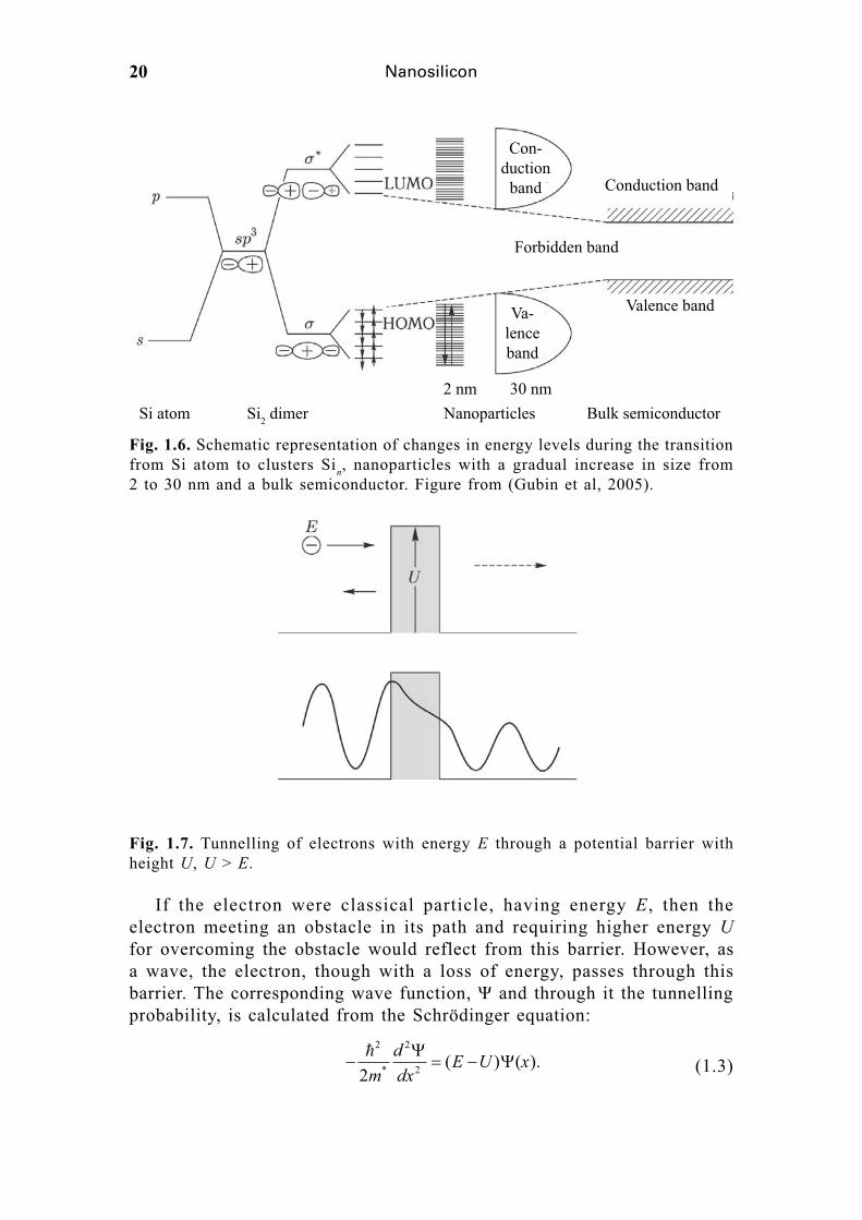
20 Nanosilicon
If the electron were classical particle, having energy E, then the electron meeting an obstacle in its path and requiring higher energy U for overcoming the obstacle would reflect from this barrier. However, as a wave, the electron, though with a loss of energy, passes through this
probability, is calculated from the Schrödinger equation:
− = −2 2
22mddx
E U x* ( )ΨΨ( ). (1.3)
Si atom Si2 dimer??????
Nanoparticles Bulk semiconductor
Va-lenceband
Valence band
Forbidden band
Conduction band
Con-duction
band
2 nm 30 nm
Fig. 1.6. Schematic representation of changes in energy levels during the transition from Si atom to clusters Sin, nanoparticles with a gradual increase in size from 2 to 30 nm and a bulk semiconductor. Figure from (Gubin et al, 2005).
Fig. 1.7. Tunnelling of electrons with energy E through a potential barrier with height U, U > E.

21Some Properties of Semiconductors – Terminology
Fig. 1.8. Single-electron tunnelling in the Coulomb blockade: 1 – conductor layer 2 – layer of insulator, 3 – tunnelling electron. Figure from (Borisenko, 1997).
This probability is higher, the thinner the barrier and the smaller the difference between the energy of the incident electron and the barrier height. The quantum constraint, which manifests itself in nanoscale structures, imposes a specific imprint on the tunnelling. Thus, the quantization of energy states of electrons in very thin, periodically spaced potential wells leads to the fact that tunnelling through them becomes resonant, i.e. only electrons with a certain energy can tunnel through such a structure.

22 Nanosilicon
Another specific manifestation of the quantum constraint is single-electron tunnelling in Coulomb blockade conditions. To explain this term, consider illustrated in Fig. 1.8 an example of passing of the electron through the metal–insulator–metal structure. As an illustration, the figure show also an analogy with a droplet coming off the edge of a tube. Initially, the interface between the metal and the dielectric is electrically neutral. When applying a potential to metallic regions a charge will start to accumulate at this boundary. It lasts as long as its value can be no longer sufficient for the separation and tunnelling through of a single electron the dielectric. After the act of tunnelling, the system returns to its original state. When the external applied voltage is conserved the entire process is repeated again. Thus, the charge transport in this structure is carried out in portions, equal to the charge of one electron. The process of charge accumulation and the detachment of an electron from the metal–dielectric boundary is determined by the balance of forces of the Coulomb interaction of electrons with other mobile and fixed charges in the metal.
In the quantum constraint mode one can artificially create materials with the properties intermediate between those of molecules and bulk material. This gives tremendous flexibility in the design of materials with special properties and a lot of potentially useful new applications for semiconductor materials.
The considered quantum effects are already being used in the currently available nanoelectronic components for information systems (Koshida, 2009; Pavesi & Turan, 2010). However, it should be emphasized that they do not exhaust all the possibilities of utilizing the quantum behaviour of electrons in instruments. Active exploratory research in this area continues today. Recently developed nanoelectronic elements due its small size, speed and power consumption are serious competition to traditional solid-state transistors and integrated circuits based on them as the main elements of information systems. Already, technology is very close to the theoretical possibility to remember and to transmit data 1 bit of data (0 and 1) with a single electron whose location in space can be defined by a single atom.
1.5.1. Luminescence of indirect-gap semiconductors
The intensity of luminescence is high for direct-gap semiconductors which include, for example, compounds such as AIIIBV, widely used for the manufacture of LEDs. In contrast, in the indirect-gap semiconductors, which include silicon, the luminescence intensity is negligible, i.e. it is very difficult to make them glow. The reason for this can be understood by referring to the energy diagram of an excited indirect-gap semiconductor, i.e. the dependence of the energy of an electron in a crystal on its quasi-momentum (Kashkarov, 2001). For single-crystal Si, this dependence is well known and is shown in Fig. 1.9. In indirect-gap semiconductors, the

23Some Properties of Semiconductors – Terminology
energy extrema of the valence band and the conduction band are shifted as regards the momentum relative to each other (curves 2 and 1 in Fig. 1.9).
As with all semiconductors, the branches of allowed states – the conduction band Ec(P) and the valence band Ev(P) – are split by the band gap Eg0 (Eg0crystal at room temperature occurs at the transitions of electrons from the branch levels Ec(P) to the branch levels Ev(P). In the non-degenerate excited material the states at the bottom of the conduction band Ec are filled (point 1), and those at the top of the valence band Ev are vacant (point 2) – Fig. 1.9.
In the investigated transition the conservation laws of energy and quasi-momentum must be satisfied:
E E Ec v
c v
1 2
1
− =
− =ph ,
,P P P2 ph
(1.4)
where Eph and Pph are the photon energy and quasi-momentum, as since Pph Pc1, we can consider Pph
Silicon is a typical indirect-gap semiconductor, i.e, the absolute minimum of the c-band is shifted with respect to the absolute maximum of of he v-band along the momentum axis. Consequently, quasi-momentum
banned. Such a process can be implemented in indirect-gap semiconductors can be only with the participation of the third particle – phonon, which reduces the probability of transition by two orders of magnitude (i.e. 100 times) compared with the case of direct-gap materials (e.g. GaAs). As a
Fig. 1.9. The dependence of the electron energy E of the quasi-momentum P for single crystal (graphics Ec(P)Ev(P)) and a silicon quantum wire (graphics E'c (P)E'v(P)) Figure from (Kashkarov, 2001).

24 Nanosilicon
photoluminescence (PL) – emission of light under the influence of optical excitation – in c-Si at not too high excitation levels is only 10–4 %. Consequently, a single photon is emitted per million of exciting photons absorbed in Si, and the PL is usually observed at low temperatures (T = 4–80 K). The energy of the emitted photons is close to Eg0 and falls on the near infrared range.
Fortunately, this is not the end for the applications of silicon as a luminescent material. There are ways in which silicon can be made to luminesce efficiently in the visible region. These methods are discussed, for example, in a review article (Kashkarov, 2001) or in a monograph (Khriachtchev, 2009).
The electronic properties of silicon can be changed by the formation of Si-based nanostructures – spatially separated Si regions with minimum dimensions of several nanometers. In this case, the charge carriers (electrons and holes) acquire additional energy due to the previously considered quantum size effect, leading to an increase in the band gap of the nanostructure compared to the single crystal of this material (Eg0), in particular for the quantum well:
′ = + +E Em d m dg g
n p0
2 2
2
2 2
22 2π π , (1.5)
where h –34 mn and mp are the effective masses of the electron and the hole, respectively, d is width of the well.
It is important to note that in silicon a decrease of the size of is accompanied by the shift of the absolute minimum of the conduction band to the left, thereby reducing the difference of the quasi-momenta in the initial 1' and the final 2' states (see Fig. 1.9). In addition, manifestation of the Heisenberg uncertainty becomes visible for nanostructures:
Δpx ⋅ Δ =x , (1.6)
and the law of conservation of the quasi-momentum is no longer strict. These reasons substantially increase the probability of optical transitions and determine the shift of the PL spectrum to the visible region.
Unfortunately, the technology for creating nanostructures in the form of so-called quantum wells, wires and dots (or thin films, wires and tiny crystals embedded in another substance) is rather complicated and not yet developed to the level of mass production. In addition, the results obtained so far do not suggest any practical industrial application of these silicon structures in the light-emitting semiconductor devices. However, the available studies give grounds for optimism (Khriachtchev, 2009).
As early as 1956 A. Uhlir (Uhlir, 1956) produced the so-called porous silicon. This material was a single-crystal silicon (mc-Si) and its surface contained a huge number of tiny pores as a result of electrochemical etching. The density of pores in some samples was so large that they

25Some Properties of Semiconductors – Terminology
overlapped and the uneteched silicon sites were in the form of coral-like filaments of variable cross sections (Fig. 1.10).
The minimum dimensions of the cross section of silicon filaments and isolated areas (clusters) in the porous layer equal, according to electron microscopic data, the units of nanometers. Porous silicon is usually formed as a layer on the surface of the mc-Si wafer, which is very convenient for use in microelectronics. Thus, methods for producing porous silicon from single crystal wafers provide the technological prerequisites for the production of nanocrystalline silicon structures by a relatively simple method.
At the end of 1990 there was a real sensation in the science of semiconductors. Lee Canham, a researcher from the UK, reported (Canham, 1990) the observation of an effective red-orange photoluminescence from porous silicon at room temperature, the yield of which amounted to 1–10%. In this publication he presented graphs of the efficiency of the photoluminescence (PL) and its shift from the infrared to the red range with increasing porosity of the sample. This connection with porosity, and hence the size of particles allowed the author to suggest that the cause of the luminescence was associated with dimensional quantum constraints.The results were of considerable interest to experts and soon a report was published on the observation of electroluminescence (EL) in porous silicon (Canham et al, 1992; Halimaoui et al, 1991). In EL light emission occurs as a result of the passage of electric current in the semiconductor, leading to excitation of electrons and holes and their subsequent recombination.
Fig. 1.10. Scheme of the formation of nanowires on the surface of a single crystal Si wafer by the merger of the surface pores created by electrochemical anodic etching of the wafer. Figure from (Kashkarov, 2001).
1–5 nm
1–10
0 μm

26 Nanosilicon
1.6. The surface and surface states
Moving to the discussion of nanomaterials with particle sizes of a few nanometers, in which the surface area reaches up to hundreds of square meters per gram, we certainly can not ignore the consideration of problems associated with the surface.
The surface is different from the volume by the fact that, in principle, it is a defect in the crystal structure, along with such well-known two-dimensional crystal structure defects as stacking faults and twins. Planes of atomic positions in which the crystal ends or meets another plane of the crystal are also defective. In the first of these cases the defect is the surface, in the second – the interface or grain boundaries. Surface atoms do not have a four-sided environment, they have unsaturated dangling bonds, which leads to the appearance of the structure of the levels in the band gap of the semiconductor. These levels in the band gaps are called surface states (Seeger, 1977).
In a bounded crystal there are not only the quantum states of electrons moving in the crystal, but also additional states in which electrons are localized on the surface of the crystal (Bonch-Bruevich and Kalashnikov, 1977, Seeger, 1977). The presence of local surface levels of energy causes that the electrons and holes can ‘stick’ to the surface, forming the surface electric charge. The surface here is the induced charge in the bulk of equal magnitude and opposite in sign, i.e. there are enriched or poor near-surface layers.
Localized electronic states form on the crystal surface; they can be proper, i.e. caused by the breakage of the crystal lattice at the boundary, and improper, localized at impurities or defects on the surface or in a layer covering the surface (e.g. oxide layer). The proper surface states form permitted energy bands separated by forbidden bands, and the wave vectors of the wave functions of these states are located in the plane tangent to the surface. The permitted surface bands may be located at in energy ranges corresponding to both forbidden and permitted three-dimensional bands. The existence of surface states was explained by Tamm (1932) based on the difference between the heights of potential barriers for an electron in the wells on the surface and in the bulk of the crystal, so that their proper surface states are called Tamm states. The electron in the Tamm state resembles a float on the surface water: it can move freely along the surface, but it can not go into the interior of the crystal not escape from it. Electrons appear to adhere to the surface.
1.6.1. Reconstruction of the surface
In real crystals, the Tamm states correspond to dangling (unsaturated) valence bonds of the surface atoms. Usually breaking of the valence bonds leads to a restructuring referred to as surface reconstruction as a result of

27Some Properties of Semiconductors – Terminology
which the lattice symmetry of the surface layer is very different from the structure of the crystal lattice in the bulk of the single crystal (Kaxiras, 2003). It should be noted that the nature of the surface reconstruction depends on the characteristics of the system and is very different from metals and semiconductors. Restructuring can be expressed in a small displacement of the atoms in comparison with the positions characteristic of the crystal, and this restructuring is called ‘surface relaxation’. However, the restructuring also called ‘surface reconstruction’ is expressed in a radical change in the atomic structure of the surface compared to the structure inside the crystal volume.
During the reconstruction the surface atoms are displaced in both the surface plane and perpendicular to the surface (Fig. 1.11); consequently, atomic structures with a period of several periods of the three-dimensional lattice or incommensurate with it form on the surface. The phenomenon of surface reconstruction is characterized primarily for crystals with covalent bonds, which include silicon.
On the clean surface of the crystal in a vacuum, immediately after its formation the atoms have broken bonds, which tend to saturate. If the surface contains no impurity atoms, which could saturate these dangling bonds, then the electrons in these bonds have only one opportunity for pairing: to form additional bonds between the surface atoms themselves. In the simplest case, the neighbouring atoms of the surface layer are combined into pairs, which are called dimers in solid state physics (by analogy with the terminology used in chemistry). The atoms of each dimer come closer to each other, while moving away from the adjacent surface atoms that are included in other dimers (Fig. 1.11). This changes the period of the crystal lattice on the surface.
In this simplest case, the surface aligns herself only after the shift to the distance between the centres of neighboring dimers, which is twice
Fig. 1.11. An example of the formation of atomic dimers in the reconstruction of the surface of type (2 × 1). The arrows show the bonds in dimers.

28 Nanosilicon
the lattice period in the inner layers. This reconstruction is denoted by (2 × 1). The symbols (n1 × n2), where n1 and n2 are the ratios of the lengths of the periods of the identity of the axes 1 and 2 of the planar reconstructed surface lattice to the lengths of the periods of identity in the same direction in the ideal unreconstructed lattice in the bulk crystal, and are often used to describe the disparity of the epitaxial crystalline layers. In the above case, the symbol (2 × 1) indicates that the period along one of the directions on the surface has doubled, and along the other remained unchanged. Figure 1.11 shows that in reconstruction the atoms are displaced both in the surface plane and perpendicular to the surface.
The nature of the reconstruction depends on the crystallographic orientation of the surface and the method of its preparation, in particular, on the purity or impurity. For example, in the atomically pure silicon crystal (see Pikus, 1992; Kaxiras, 2003) the reconstruction leads to the formation on the surface (111) of a structure with periods (1 × 1), (2 × 1), (7 × 7) and on the surface (100) – structures (2 × 1), (4 × 2), (2 × 2). If the surface adsorbs hydrogen atoms, compensating dangling bonds, then the structures with periods (1 × 1), (3 × 1) form the (100) surface.
The nature of surface reconstruction has a significant influence on the spectrum of the surface states E(k ||) – dependence of energy on the wave vector parallel to the surface. The spectrum of surface states depends strongly on the orientation of the surface and its purity.
Surface energy levels can significantly alter the kinetics of electronic processes, since they create additional recombination centres and generation of charge carriers. Therefore, all the phenomena associated with non-equilibrium electrons and holes, such as photoconductivity and photovoltage, depend on the condition of the surface.
In addition, the surface usually accumulate surface excitons, the wave function of which is also localized near the boundary of the crystal. Due to the transition of electrons to surface states the electron concentration at the semiconductor surface is very different from the electron concentration in the crystal. The surface layer may have a conductivity much higher than the bulk conductivity. The change of electron concentration in the direction to the surface leads to the bending of energy bands, and sufficiently strong bending may change the very type of conductivity in the surface layer and the so-called inversion layer forms there.
Concluding remarks
In the following chapters of this monograph we will discuss in greater detail the properties of silicon nanoparticles characterized by the effects mentioned here determined by quantum constraints, methods for the preparation of nanoparticles of the required configuration and dimensions, as well as the areas of application of these materials that are already being implemented in practice, and those that may be developed in the near future. In the
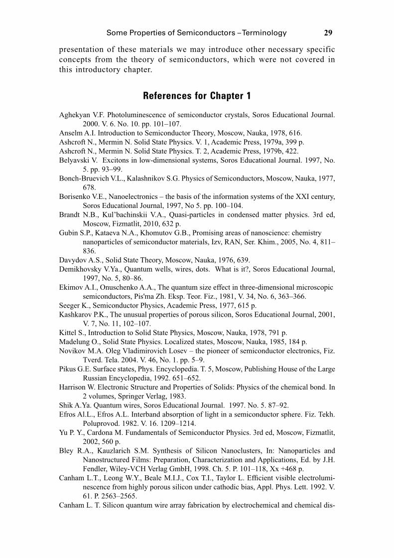
29Some Properties of Semiconductors – Terminology
References for Chapter 1
Aghekyan V.F. Photoluminescence of semiconductor crystals, Soros Educational Journal. 2000. V. 6. No. 10. pp. 101–107.
Anselm A.I. Introduction to Semiconductor Theory, Moscow, Nauka, 1978, 616.Ashcroft N., Mermin N. Solid State Physics. V. 1, Academic Press, 1979a, 399 p.Ashcroft N., Mermin N. Solid State Physics. T. 2, Academic Press, 1979b, 422.Belyavski V. Excitons in low-dimensional systems, Soros Educational Journal. 1997, No.
5. pp. 93–99.Bonch-Bruevich V.L., Kalashnikov S.G. Physics of Semiconductors, Moscow, Nauka, 1977,
678.Borisenko V.E., Nanoelectronics – the basis of the information systems of the XXI century,
Soros Educational Journal, 1997, No 5. pp. 100–104.Brandt N.B., Kul’bachinskii V.A., Quasi-particles in condensed matter physics. 3rd ed,
Moscow, Fizmatlit, 2010, 632 p.Gubin S.P., Kataeva N.A., Khomutov G.B., Promising areas of nanoscience: chemistry nanoparticles of semiconductor materials, Izv, RAN, Ser. Khim., 2005, No. 4, 811–
836.Davydov A.S., Solid State Theory, Moscow, Nauka, 1976, 639.Demikhovsky V.Ya., Quantum wells, wires, dots. What is it?, Soros Educational Journal,
1997, No. 5, 80–86.Ekimov A.I., Onuschenko A.A., The quantum size effect in three-dimensional microscopic semiconductors, Pis'ma Zh. Eksp. Teor. Fiz., 1981, V. 34, No. 6, 363–366.Seeger K., Semiconductor Physics, Academic Press, 1977, 615 p.Kashkarov P.K., The unusual properties of porous silicon, Soros Educational Journal, 2001,
V. 7, No. 11, 102–107.Kittel S., Introduction to Solid State Physics, Moscow, Nauka, 1978, 791 p.Madelung O., Solid State Physics. Localized states, Moscow, Nauka, 1985, 184 p.Novikov M.A. Oleg Vladimirovich Losev – the pioneer of semiconductor electronics, Fiz.
Tverd. Tela. 2004. V. 46, No. 1. pp. 5–9.Pikus G.E. Surface states, Phys. Encyclopedia. T. 5, Moscow, Publishing House of the Large
Russian Encyclopedia, 1992. 651–652.Harrison W. Electronic Structure and Properties of Solids: Physics of the chemical bond. In
2 volumes, Springer Verlag, 1983.Shik A.Ya. Quantum wires, Soros Educational Journal. 1997. No. 5. 87–92.Efros Al.L., Efros A.L. Interband absorption of light in a semiconductor sphere. Fiz. Tekh.
Poluprovod. 1982. V. 16. 1209–1214.Yu P. Y., Cardona M. Fundamentals of Semiconductor Physics. 3rd ed, Moscow, Fizmatlit,
2002, 560 p.Bley R.A., Kauzlarich S.M. Synthesis of Silicon Nanoclusters, In: Nanoparticles and
Nanostructured Films: Preparation, Characterization and Applications, Ed. by J.H. Fendler, Wiley-VCH Verlag GmbH, 1998. Ch. 5. P. 101–118, Xx +468 p.
electrolumi-nescence from highly porous silicon under cathodic bias, Appl. Phys. Lett. 1992. V. 61. P. 2563–2565.
Canham L. T. Silicon quantum wire array fabrication by electrochemical and chemical dis-
presentation of these materials we may introduce other necessary specific concepts from the theory of semiconductors, which were not covered in this introductory chapter.

30 Nanosilicon
solution of wafers, Appl. Phys. Lett. 1990. V. 57. P. 1046–1048.Halimaoui A., Oules C., Bomchil G., Bsiesy A., Gaspard F., Herino R., Ligeon M., Muller F.
Electroluminescence in the visible range during anodic oxidation of porous silicon
Hamaguchi C. Basic Semiconductor Physics. 2 ed, Springer, 2010, 570 p.Kaxiras E. Atomic and electronic structure of solids. Cambridge University Press, 2003,
696 p.Khriachtchev L. (Ed.). Silicon nanophotonics: Basic principles, present status and perspe-
Koshida N. (Ed.). Device applications of silicon nanocrystals and nanostructures, Springer, 2009. Xii +344 p.Moliton A., Solid-state physics for electronics, Wiley-ISTE, 2009, Xvi +389 p.Pavesi L., Turan R. (Eds). Silicon Nanocrystals: Fundamentals, synthesis and applications.Wiley-VCH Verlag GmbH & Co, 2010, XXI +627 p.Uhlir A., Electrolytic shaping of germanium and silicon, Bell System Technical Journal.
1956. V. 35. P. 333–347.Yacobi B.G. Semiconductor materials: An introduction to basic principles, Kluwer Aca-
demic Publishers, 2004, Ix +228 p.Yu P. Y., Cardona M. Fundamentals of Semiconductors, Graduate Texts in Physics. 4 ed.,
Berlin–Heidelberg, Springer–Verlag, 2010, 775 p.