nanotechnology at ntnu 2003 - norges forskningsråd o… · nanotechnology at ntnu 2003 ......
TRANSCRIPT
NTNU
Nanotechnology
at NTNU
2003
The Norwegian University ofScience and Technology

PREFACE
The Committee appointed by the rektor at NTNU, Eivind Hiis Hauge, for the evaluation andplanning of activities within nanotechnology at NTNU, hereby submits its report.
The Committee has carried out one site-visit over two days following initial writteninformation concerning ongoing nanotechnochnology activity at NTNU, and status and plansat the Norwegian Microtechnology Center, Oslo. The site-visit included presentations byselected faculty members of research projects and plans, and visits to various laboratories.
The Committee gratefully acknowledges all those involved in the task, in particular facultyand staff actively contributing to make the site-visit a fruitful basis for discussion andcompletion of the report.
Strasbourg/Delft/Dresden/Oslo/TrondheimApril 2003
Thomas W. Ebbesen J.E. Mooij Frank Jülicher
Anders Hanneborg Mari-Ann Einarsrud Jostein Grepstad
Bjørn T. Stokke
Nanotechnology at NTNU The Norwegian University of Science and Technology Page 3
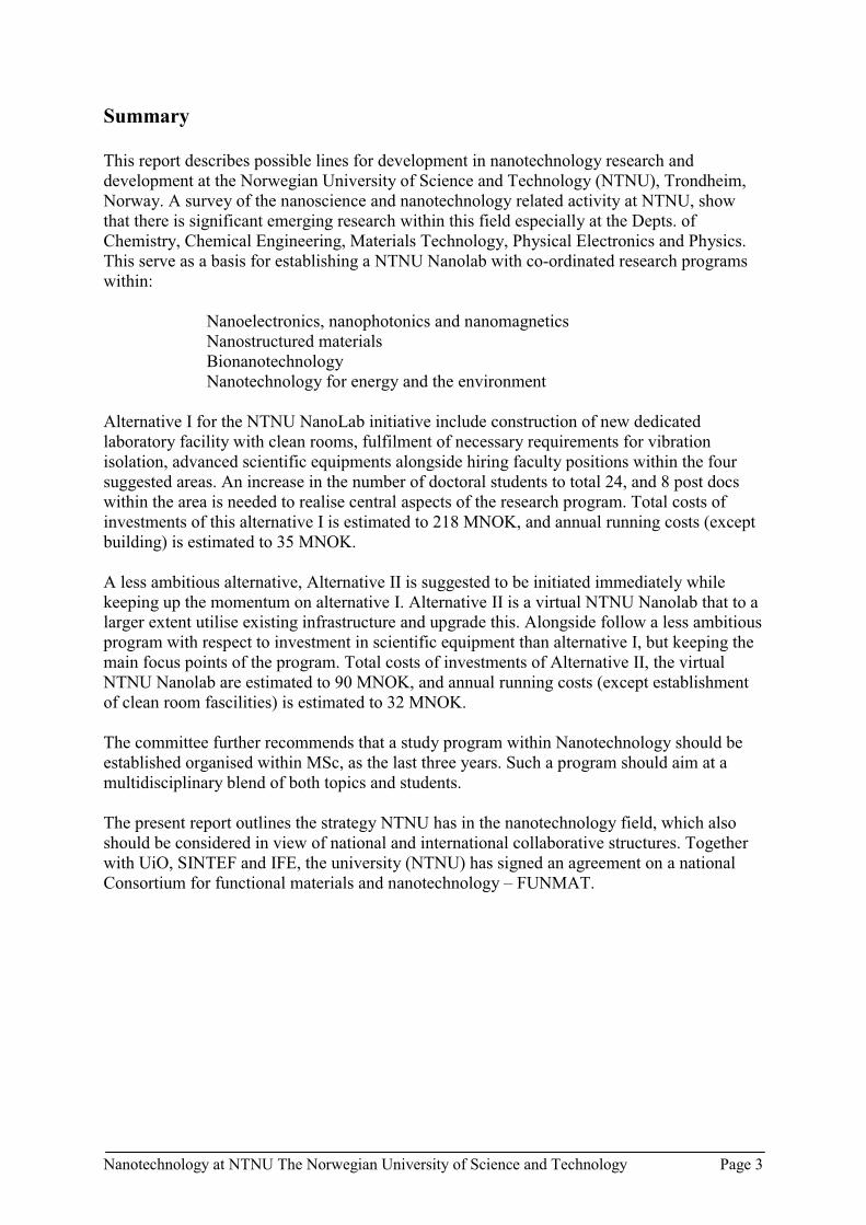
Summary
This report describes possible lines for development in nanotechnology research anddevelopment at the Norwegian University of Science and Technology (NTNU), Trondheim,Norway. A survey of the nanoscience and nanotechnology related activity at NTNU, showthat there is significant emerging research within this field especially at the Depts. ofChemistry, Chemical Engineering, Materials Technology, Physical Electronics and Physics.This serve as a basis for establishing a NTNU Nanolab with co-ordinated research programswithin:
Nanoelectronics, nanophotonics and nanomagneticsNanostructured materialsBionanotechnologyNanotechnology for energy and the environment
Alternative I for the NTNU NanoLab initiative include construction of new dedicatedlaboratory facility with clean rooms, fulfilment of necessary requirements for vibrationisolation, advanced scientific equipments alongside hiring faculty positions within the foursuggested areas. An increase in the number of doctoral students to total 24, and 8 post docswithin the area is needed to realise central aspects of the research program. Total costs ofinvestments of this alternative I is estimated to 218 MNOK, and annual running costs (exceptbuilding) is estimated to 35 MNOK.
A less ambitious alternative, Alternative II is suggested to be initiated immediately whilekeeping up the momentum on alternative I. Alternative II is a virtual NTNU Nanolab that to alarger extent utilise existing infrastructure and upgrade this. Alongside follow a less ambitiousprogram with respect to investment in scientific equipment than alternative I, but keeping themain focus points of the program. Total costs of investments of Alternative II, the virtualNTNU Nanolab are estimated to 90 MNOK, and annual running costs (except establishmentof clean room fascilities) is estimated to 32 MNOK.
The committee further recommends that a study program within Nanotechnology should beestablished organised within MSc, as the last three years. Such a program should aim at amultidisciplinary blend of both topics and students.
The present report outlines the strategy NTNU has in the nanotechnology field, which alsoshould be considered in view of national and international collaborative structures. Togetherwith UiO, SINTEF and IFE, the university (NTNU) has signed an agreement on a nationalConsortium for functional materials and nanotechnology – FUNMAT.
Nanotechnology at NTNU The Norwegian University of Science and Technology Page 4
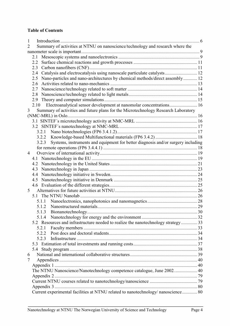
Table of Contents
1 Introduction ........................................................................................................................ 62 Summary of activities at NTNU on nanoscience/technology and research where thenanometer scale is important...................................................................................................... 9
2.1 Mesoscopic systems and nanoelectronics ...................................................................... 92.2 Surface chemical reactions and growth processes ....................................................... 112.3 Carbon nanofibers (CNF)............................................................................................. 112.4 Catalysis and electrocatalysis using nanoscale particulate catalysts............................ 122.5 Nano-particles and nano-architectures by chemical methods/direct assembly............ 122.6 Activities related to nano-mechanics ........................................................................... 132.7 Nanoscience/technology related to soft matter ............................................................ 142.8 Nanoscience/technology related to light metals........................................................... 142.9 Theory and computer simulations ................................................................................ 152.10 Electroanalytical sensor development at nanomolar concentrations........................ 16
3 Summary of activities and future plans for the Microtechnology Research Laboratory(NMC-MRL) in Oslo................................................................................................................ 16
3.1 SINTEF´s microtechnology activity at NMC-MRL ..................................................... 163.2 SINTEF´s nanotechnology at NMC-MRL................................................................... 17
3.2.1 Nano biotechnologies (FP6 3.4.1.2)..................................................................... 173.2.2 Knowledge-based Multifunctional materials (FP6 3.4.2) .................................... 183.2.3 Systems, instruments and equipment for better diagnosis and/or surgery includingfor remote operations (FP6 3.4.4.1) ................................................................................. 18
4 Overview of international activity.................................................................................... 194.1 Nanotechnology in the EU ........................................................................................... 194.2 Nanotechnology in the United States ........................................................................... 214.3 Nanotechnology in Japan ............................................................................................. 234.4 Nanotechnology initiative in Sweden........................................................................... 244.5 Nanotechnology initiative in Denmark ........................................................................ 254.6 Evaluation of the different strategies............................................................................ 25
5 Alternatives for future activities at NTNU....................................................................... 265.1 The NTNU Nanolab ..................................................................................................... 26
5.1.1 Nanoelectronics, nanophotonics and nanomagnetics........................................... 285.1.2 Nanostructured materials...................................................................................... 295.1.3 Bionanotechnology............................................................................................... 305.1.4 Nanotechnology for energy and the environment ................................................ 32
5.2 Resources and infrastructure needed to realize the nanotechnology strategy.............. 335.2.1 Faculty members .................................................................................................. 335.2.2 Post docs and doctoral students............................................................................ 345.2.3 Infrastructure ........................................................................................................ 34
5.3 Estimation of total investments and running costs....................................................... 375.4 Study program .............................................................................................................. 38
6 National and international collaborative structures.......................................................... 397 Appendices ....................................................................................................................... 40
Appendix 1 ........................................................................................................................... 40The NTNU Nanoscience/Nanotechnology competence catalogue, June 2002.................... 40Appendix 2 ........................................................................................................................... 79Current NTNU courses related to nanotechnology/nanoscience ......................................... 79Appendix 3 ........................................................................................................................... 80Current experimental facilities at NTNU related to nanotechnology/ nanoscience............. 80

Nanotechnology at NTNU The Norwegian University of Science and Technology Page 5
Appendix 4 ........................................................................................................................... 82Expression of interests filed to EU 6th Framework program - participation from NTNUwithin the field of Nanotechnology...................................................................................... 82Appendix 5 ........................................................................................................................... 83Agenda from site visit. ......................................................................................................... 83

Nanotechnology at NTNU The Norwegian University of Science and Technology Page 6
1 Introduction
Nanotechnology can be viewed as the technology for the creation and utilization of materials,devices, and systems where control of matter and tolerances at the nanometer-length scale isessential for their properties. This length scale implies engineering on the level of atoms,molecules, and supramolecular structures. Nanotechnology, as the field stands today, has notemerged from a paradigm shift in science such as e.g. functional genomics that gainedsubstantial momentum following the complete sequencing of various genomes.Nanotechnology has evolved from scientific disciplines such as chemistry, physics, materialsscience, biology, medicine, and electronics engineering, which already include a significantcomponent as far as control of matter on the nanometer length scale. Although a more or lesscontinuous evolution of this field can be identified, a few milestone developments driving theadvancement of nanoscience and nanotechnology is highlighted below.
One of the 20th century hallmark science lectures, “There is plenty of room at the bottom”,was given by the late Nobel laureate Richard Feynman in 1959 at the California Institute ofTechnology. In this famous lecture, Prof. Feynman put forward a vision of exciting newdiscoveries related to the manufacture of materials and devices at the nanometer scale. Heargued that it was possible to write all 25000 pages of the Encyclopedia Britannica within anarea of a pinhead, e.g. by an electron beam that could write lines in materials. Thisexpectation was realized some thirty years later when researchers at IBM’s AlmadenResearch center where able to control the location of individual atoms on a surface andspelled the logo of the company with a size less than 3 x 3 nm squared for an arrangement ofthe 35 atoms.
The IBM researchers used a tool developed from the scanning tunneling microscope (STM).The STM and later developments based on this invention, scanning probe microscopes,sensing e.g. various type of forces, topographies, temperature, electrical potentials andmagnetic fields with high positional resolution, are considered milestones in the history ofnanotechnology. These scanning probe microscopes not only allow observation of atoms andtheir properties either alone or as members of larger structural arrangements, but also permitcontrol the atomic and molecular positions in assembling structures with nanometer precision.The approach used in generating the nanometer sized IBM logo by locating the position ofsingle atoms using a tool controlled by humans can be viewed as the ultimate realization ofthe top-down approach of molecular construction. Top-down approaches traditionally includecarving, milling and photolitography to structure bits and pieces from a larger workpiece. Thetool of miniaturisation in the semiconductor industry has moved from optical to UV to X-rayand e-beam based lithographic techniques and constitute important examples of manufactureby top-down approaches. Moreover, this industry is a main driving force for the developmentof new concepts, because further miniaturisation is expected to encounter “roadblocks” forwhich there are no known solutions, in a 10 years perspective.
The other main class of techniques for construction of nanometer sized structures is based onself-assembly, or other bottom-up approaches. Materials synthesis by self-assembly at thesub-micron length scale is abundant in nature, and the nanostructuring of the chemicalcomponents obtained can display vastly improved properties compared to what humans haveachieved so far. One example is the organization of calcium carbonate found in abaloneshells, providing far better mechanical strength and crack properties than found e.g. in chalkto be used on the blackboard. The abalone shell additionally uses biological polymers,proteins and polysaccharides in order to organize the calcium carbonate. Another biological

Nanotechnology at NTNU The Norwegian University of Science and Technology Page 7
ingenious self-assembled structure is the F1 part of the ATP-ase. This protein structurefunction as a nano-engine driven by a gradient in proton concentration converting thechemical potential to chemically stored energy by a /3 stepwise rotation of a shaft in thecomplex. The rotaxanes, where a hydrophobic tail is treaded in the interior of thecyclodextrins, yielding a similar structural basis for rotary motion of a molecular shaft appearto be highly inspired by the F1-ATP-ase. Another example of man-made self-assemblednanostructures is the highly oriented carbon-nanotubes created at Harvard University.
A third milestone providing impetus for nanotechnology, is the speech given by US PresidentWilliams J. Clinton, on 21 Jan 2000 at California Institute of Technology, launching theNational Nanotechnology Initiative. An excerpt from this speech reads:
“My budget supports a major new National Nanotechnology Initiative, worth $500
million. …the ability to manipulate matter at the atomic and molecular level. Imagine
the possibilities: materials with ten times the strength of steel and only a small fraction
of the weight – shrinking all the information housed at the Library of Congress into a
device the size of a sugar cube – detecting cancerous tumors when they are only a few
cells in size. Some of our research goals may take 20 or more years to achieve, but
that is precisely why there is an important role for the federal government.”
The selected examples emphasize symbolic milestones for the development ofnanotechnology and identify the three mutually dependent factors for advancement of thefield: ideas, tools, and funding. A main factor in obtaining funding for development withinnanotechnology is found both within gaining new fundamental knowledge and within possibleapplications and ultimately market for the products. Control of matter at the atomic ormolecular level implies tailoring the fundamental properties, phenomena, and processesexactly at the scale where the basic properties are determined. In this context, nanotechnologycould impact the production of almost all objects produced by humans, from tires andtransportation system, cleaning of exhaust fumes by nanostructured catalysts to computercircuits and sensors, from personalized medicines to tailored tissue replacements.
Nanotechnology is a branch of science and engineering in rapid growth, which is expected tohave enormous impact on society throughout the 21st century. To illustrate theseexpectations, we cite The National Nanotechnological Inititative (NNI), USA: “The impact of
nanotechnology on health, wealth, and lives of people could be at least as significant as the
combined influences of microelectronics, medical imaging, computer-aided engineering, and
man-made polymers developed in the century just past”1.
The European Union places emphasis on nanotechnology and functional materials byallocating significant funding for research in this field. Sweden has established their“Nanonetverk” placing this area of research high on the agenda, while in Norway there is sofar no strong concerted action.
A committee appointed by Rektor Eivind Hiis Hauge at the Norwegian University of Scienceand Technology (NTNU), Trondheim with a commission to provide an overview of
1 National Nanotechnology Initiative. The initiative and its implementation plan. Detailed technical reportassociated with the supplemental report to the President’s FY 2003 budget. National Science and TechnologyCouncil.
Nanotechnology at NTNU The Norwegian University of Science and Technology Page 8
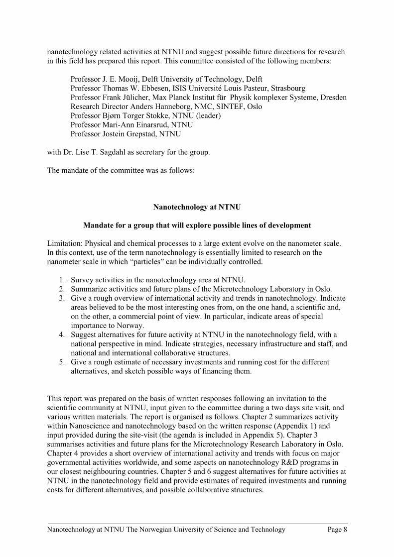
nanotechnology related activities at NTNU and suggest possible future directions for researchin this field has prepared this report. This committee consisted of the following members:
Professor J. E. Mooij, Delft University of Technology, DelftProfessor Thomas W. Ebbesen, ISIS Université Louis Pasteur, StrasbourgProfessor Frank Jülicher, Max Planck Institut für Physik komplexer Systeme, DresdenResearch Director Anders Hanneborg, NMC, SINTEF, OsloProfessor Bjørn Torger Stokke, NTNU (leader)Professor Mari-Ann Einarsrud, NTNUProfessor Jostein Grepstad, NTNU
with Dr. Lise T. Sagdahl as secretary for the group.
The mandate of the committee was as follows:
Nanotechnology at NTNU
Mandate for a group that will explore possible lines of development
Limitation: Physical and chemical processes to a large extent evolve on the nanometer scale.In this context, use of the term nanotechnology is essentially limited to research on thenanometer scale in which “particles” can be individually controlled.
1. Survey activities in the nanotechnology area at NTNU.2. Summarize activities and future plans of the Microtechnology Laboratory in Oslo.3. Give a rough overview of international activity and trends in nanotechnology. Indicate
areas believed to be the most interesting ones from, on the one hand, a scientific and,on the other, a commercial point of view. In particular, indicate areas of specialimportance to Norway.
4. Suggest alternatives for future activity at NTNU in the nanotechnology field, with anational perspective in mind. Indicate strategies, necessary infrastructure and staff, andnational and international collaborative structures.
5. Give a rough estimate of necessary investments and running cost for the differentalternatives, and sketch possible ways of financing them.
This report was prepared on the basis of written responses following an invitation to thescientific community at NTNU, input given to the committee during a two days site visit, andvarious written materials. The report is organised as follows. Chapter 2 summarizes activitywithin Nanoscience and nanotechnology based on the written response (Appendix 1) andinput provided during the site-visit (the agenda is included in Appendix 5). Chapter 3summarises activities and future plans for the Microtechnology Research Laboratory in Oslo.Chapter 4 provides a short overview of international activity and trends with focus on majorgovernmental activities worldwide, and some aspects on nanotechnology R&D programs inour closest neighbouring countries. Chapter 5 and 6 suggest alternatives for future activities atNTNU in the nanotechnology field and provide estimates of required investments and runningcosts for different alternatives, and possible collaborative structures.

Nanotechnology at NTNU The Norwegian University of Science and Technology Page 9
2 Summary of activities at NTNU on nanoscience/technology and research
where the nanometer scale is important
Names of the faculty members in charge of the activities/projects are reported. Names of postdocs are given in italics. The number of manyears for dr. students, post docs and otherresearchers working in the field of nanotechnology for each group reported per June 2002 isalso included. Number of M. Sc. students is not reported. Some comments stated by thenanotechnology committee are also included in this summary.
2.1 Mesoscopic systems and nanoelectronics
The “roadmap” of the Semiconductor Industry Association (SIA) shows that currentexponential increase in performance per unit cost of integrated electronic circuits, commonlyreferred to as Moore’s law, will come to an end within 10 years, unless technical barriers withno known solutions are surmounted. This challenge will demand the development andunderstanding of new materials and hybrid devices at an unprecedented pace and explainswhy this industry now takes a keen interest in mesoscopic physics and nanotechnology.
Modification of material properties by nanostructuring remains a current trend in solid statetechnology (the concept of “quantum design”). These mesoscopic systems display a variety of(novel) physical phenomena, e.g. quantum confinement, quantum Hall effect, spinpolarization and Coulomb blockade. Improved understanding and more accurate physicalmodels are called for in order to exploit these phenomena for new electronic, photonic deviceapplications, such as for physical realizations of qubits. Recent developments innanotechnology make it possible to manufacture electronic devices with features as small as10 nm (nanoelectronics). The challenge is to incorporate such devices into integrated circuitsand hybrid electronic systems.
Condensed matter theory. The condensed matter theorists (Brataas, Sudbø; Dept. of Physics;dr. stud.: 0, post doc: 0, others: 0) focuses on investigating the underlying, fundamentalphysics of meso-scopic systems. The research is concentrated on developing improvedtheoretical models for describing transport and other physical phenomena in such systems,incl. normal metals, ferromagnetic metals, low-dimensional semiconductors (quantumwells/wires/dots), low-Tc and high-Tc superconductors. Investigations include spin-injectioninto such materials, which is expected to unveil a wealth of new phenomena with a potentialfor novel “spintronic” device applications, (i.e., devices which exploit the electron spin ratherthan the charge, only). The committee underlines that strengthening the link to theexperimental groups working on perovskites would be beneficial for the field of functionaloxides which has a broad and strong basis at NTNU.
Nanostructured superconductors. Superconductors are materials in which artificialmodulations on the nanometer length scale can drastically alter (improve) their criticalparameters. The superconductivity research group (Fossheim; Dept. of Physics; dr. stud.: 0.2,post doc: 0.1, others: 0) has carried out experiments along these lines for several years, withemphasis on the flux pinning properties of high- Tc superconductors. More recently, thegroup has studied quantum oscillations in the magnetic field dependent transport properties oflow- Tc superconducting (Al, Pb) thin film micro-/nanostructures. In collaboration with theepitaxial oxide thin film group (Grepstad, Tybell; Dept. of Physical Electronics; dr. stud.: 2,post doc: 1, others: 1), the experiments are now being extended to nanostructured high-Tcsuperconducting thin films, with emphasis on the transport properties in high-Tc nanowires.

Nanotechnology at NTNU The Norwegian University of Science and Technology Page 10
The development of techniques for nanoscale patterning of high-Tc thin films, as well asnanostructured growth of such films on a suitably prepared template, constitutes an essentialpart of this project.
Nanoscale etching of metallic perovskite heterostructures. The principal objective of thisproject, which is a collaboration between groups in physics (Borg; Dept. of Physics; dr. stud.:1, post doc: 0, others: 0) and physical electronics (Grepstad, Tybell; Dept. of PhysicalElectronics; dr. stud.: 2, post doc: 1, others: 1), is to explore the case for using a scanningtunneling microscope to create nanostructured templates of metallic perovskite thin films, forsubsequent growth of perovskites with different functionalities.
Ferroelectric perovskite heterostructures with local control of polarization. Materials withlarge electromechanical coupling are essential to sensors and actuators, at the core of MEMStechnology. An interesting class of materials is the perovskites, covering a broad range offunctionalities. As with microelectronics, the trend is for downscaling of ceramic devices. Byminiaturising today’s MEMS technology towards nanometer length scales (NEMS), thereduced mass and dimensions of the devices will increase the sensitivity of sensors and theresonance frequency of actuators.
A project was recently initiated (Grepstad, Tybell; Dept. of Physical Electronics; dr. stud.: 2,post doc: 1, others: 1) to study the impact of dimensionality and size on the electromechanicalproperties of ferroelectric thin films, also being piezoelectric and pyroelectric, with aperspective to develop materials with controlled functionality for future NEMS applications.This project entails the heteroepitaxial growth of perovskite multilayers/superlattices withferroelectric and dielectric materials, as well as the use of scanning probe microscopy tolocally control the ferroelectric polarization. Moreover, atomic force microscopy will be usedto study intrinsic polarization phenomena on the nanometer length scale in both simpleferroelectric perovskites, such as PbTiO3, and in artificial superlattices.
The above mentioned activities are part of a broader effort, involving groups in Physics,Materials Technology and Physical Electronics, to establish a multidisciplinary platform forresearch at NTNU on the development and control of nanoscale structures in advancedmaterials. One goal is to develop novel synthesis methods for perovskite nanostructures basedon bottomup architecture. This project opens for a closer collaboration between theorists andexperimentalists in the field of perovskites.
MBE growth of compound semiconductor nanostructures. Molecular beam epitaxy (MBE)is a powerful crystal growth technique, successfully adopted for fabrication of compoundsemiconductor devices which take advantage of quantum confinement, such as heterostructurefield effect transistors and quantum well laser diodes. The MBE group (Fimland, Rønnekleiv;Dept. of Physical Electronics; dr. stud.: 1.4, post doc: 0, others: 0) presently focuses on thefabrication of GaSb-based device structures (quantum wells and superlattices) for laser diodesemitting in the 2.02.4 �m spectral range. A closer link between theory and experimentswould be beneficial for this research.
Self-organisation in organic semiconducting thin films. Semiconducting polymericmaterials in the form of thin layers are currently being developed for use as the activeelements in allpolymeric electronics (FET’s) and light-emitting diode (LED) screens, as wellas for polymeric memories. Collaborating groups (Samuelsen; Dept. of Physics; dr. stud.: 1,post doc: 0, others: 0) and (Carlsen; Dept. of Chemistry) have discovered a pronounced self-

Nanotechnology at NTNU The Norwegian University of Science and Technology Page 11
organisation in such films, for film thicknesses less than 200 nm, with direct implications forthe performance of thin layer FET’s and LED’s. This self-organisation is presently beinginvestigated from a fundamental physics point of view and as a useful tool in materialsdevelopment. The group uses a Langmuir technique to obtain ordered films with thicknessesdown to less than 10 nm. The committee wants to point out that a possible collaboration withthe theorists at Dept. of Chemistry might be fruitful for this activity.
2.2 Surface chemical reactions and growth processes
Surface science is a discipline of vital importance to modern industry, e.g. in catalyticchemistry, in tribology, and in microelectronics. The physical and chemical properties ofsurfaces (electronic structure, optical reflectivity, friction, chemical bonding and reactivity,etc.) evolve on a nanometer length scale. Moreover, a powerful suite of analytic and structuraltools is now available, capable of probing solid surfaces with subnanometer depth resolution.
STM studies of growth processes on the nanometer scale. Scanning tunneling microscopystudies aimed at understanding nucleation and growth behaviour on a nanometer length scalefor homo- and heteroepitaxial metal systems and for metallic clusters on oxide surfacesremain a major theme of research in the STM laboratory (Borg; Dept. of Physics; dr. stud.: 1,post doc: 0, others: 0). These studies have contributed to the understanding of how atomicprocesses affect thin film growth. Moreover, metal clusters supported by e.g. Al2O3 mayserve as model systems for fundamental research into heterogeneous catalysis.
Chemical reactions on nanostructured surface alloys. Recent studies of nano-structuredsurface alloys in the surface physics group (Raaen; Dept. of Physics; dr. stud.: 2, post doc: 1,others: 0) have shown that the physical and chemical properties of catalytically activetransition metal surfaces (e.g. Pt(111), Rh(100)) may be strongly influenced by alloying rareearths in monolayer thickness on these surfaces. The surface alloys have thicknesses typicallyless than one nanometer and have been shown to exhibit nanoscale structure also in the lateraldirections. Of special interest to the group is surface reactivity, propagating reaction fronts,and the formation of spatio-temporal concentration patterns on a mesoscopic scale. Thecommittee points out that an interesting extension of the activity of this research group isclustering on surfaces, i.e. clustering on perovskite surfaces.
2.3 Carbon nanofibers (CNF)
The main activities are production of carbon nanoparticles, nanofibers, and nanotubes. Onegroup (Holmen, Chen; Dept. of Chemical Engineering; dr. stud.: 4, post doc: 0, others: 0) usescatalytic decomposition of selected carbon-containing gases for preparation of carbonnanofibers. Hydrotalcite-delivered Ni-Cu-Al and Ni-Fe-Al catalysts have been synthesized,characterized and tested for carbon nanofiber production. This type of the catalyst makes itpossible to produce the CNF with controllable and almost uniform diameter distribution.Selecting the proper catalyst, reactant mixture and temperature controls the CNFnanostructure. A high yield of CNF has been achieved.
Another group (Bakken; Dept. of Materials Technology) is using three-phase AC plasmatechnology for large-scale production of nanostructured carbon (fullerenes, nanotubes). Thegroup is especially considering the numerical modelling and simulations of plasma/arc

Nanotechnology at NTNU The Norwegian University of Science and Technology Page 12
reactors. This group is strongly linked to SINTEF. However, the committee believes theNTNU activity is below critical mass.
The electrochemistry group (Tunold, Solberg, Hagen; Dept. of Materials Technology: dr.stud.: total 6, post doc: 6, others:0) reports on studies of carbon nanostructures for battery andgas storage applications.
2.4 Catalysis and electrocatalysis using nanoscale particulate catalysts
Electrocatalysis. Fundamental physical processes taking place on nanoscale particles arestudied by the electrochemistry group (Tunold, Hagen, Solberg, Hjelen, Nes, Arnberg, Dept.of Materials Technology; total dr. stud.: 6, post doc: 6, others: 0). These studies are ofimportance for development of environmentally friendly and reliable energy systems. Thedevelopment of active electrode materials and structures for systems including PEM waterelectrolysis and PEM fuel cells for hydrogen and hydrogen carriers requires methods forinvestigation of nanoscale systems. The noble metal catalyst particles used in energyconversion processes are metals or oxides with semiconducting properties that depend onpotential, crystallinity and structure. Adsorption of gaseous species and intermediates onnanoscale mono- and bifunctional noble metal catalysts is studied. Nucleation of adsorbates isinvestigated by chronoamperometry and the whole multi-step process is being studied andmodelled by Electrochemical Impedance Spectroscopy (EIS). The committee points out thatcollaboration with the STM-group at Dept. of Physics should be strengthened.
Catalysis on metallic nanoparticles. Catalysis on nanoparticles has recently emerged as aninteresting subject of research since metal particles with dimensions less 2-3 nm have uniqueproperties. The catalysis group (Holmen, Blekkan, Chen; Dept. of Chemical Engineering; dr.stud.: 4, post doc: 0, others: 0)) is studying bimetallic particles in the nanometer range to gaininformation about size and composition of the metallic particles in catalyst systems. Themetal particles are prepared by wet impregnation of the support and subsequent reduction.Characterisation techniques used are Scanning Transmission Electron Microscopy (STEM)(Holmestad, Høier, Tøtdal; Dept. of Physics; dr. stud.: 3, post doc: 0.5, others: .3), EnergyDispersive X-ray analysis (EDX), and X-ray Absorption Spectroscopy (XAS/EXAFS).Preparation of metal nanoparticles has been carried from hydrotalcite precursors using carbonnanofibers as template and by using a sol-gel process.
2.5 Nano-particles and nano-architectures by chemical methods/direct assembly
Chemical methods or soft chemistry routes are well-established methods for the preparationof a wide range of nanoparticles, nanorods, and nanotubes as well as films and 3-D structures.These chemistry-based methods have the advantage of featuring a high degree of flexibilityand simplicity of up-scaling. At NTNU there is research focusing on development andfabrication of novel types of nanoparticles and nano-architectures with tuneable structuralcharacteristics. These efforts are directed towards both materials science (Einarsrud, Grande,Wiik, Kaus; Dept. of Materials Technology; dr. stud.: 2.5, post doc: 1, others: 1) and theprocess industry (Sjøblom, Øye, Hemmingsen; Dept. of Chemical Engineering; dr. stud.: 0,post doc: 1.1, others: 0).
Nanotechnology at NTNU The Norwegian University of Science and Technology Page 13
Inorganic and ceramic materials. Ceramic nanoparticles and a wide range of nanostructuredceramic materials are prepared by sol-gel based and other wet chemical synthesis methods inthe materials science group (Einarsrud, Grande, Wiik, Kaus; Dept. of Materials Technology;dr. stud.: 2.5, post doc: 1, others: 1). By controlling the type of precursors used, the type ofsolvent, the use of surfactant or templates and the chemical conditions (i.e. pH andconcentrations), nanoparticles with controlled size and morphology or different controllednanostructures can be prepared. Different geometries like films, fibers and monoliths areprepared. The experimental part of the activity includes the synthesis of ceramicnanoparticles, monolithic nanostructured porous materials, porous films and organic-inorganic hybrid materials. The nanoparticles are also used as precursors for the preparationof e.g. nanocrystalline ceramic materials. In collaboration with the TEM group (Holmestad,Høier, Tøtdal; Dept. of Physics; dr. stud.: 3, post doc: 0.5, others: 0.3) the nanoparticles andnanocrystalline ceramics are studied, including the ferroelastic domain structure (nanoscaletwins) in LaCoO3 based materials.
Magnetic nanoparticle structures. The Sjøblom group (Sjøblom, Øye, Hemmingsen; Dept. ofChemical Engineering; dr. stud.: 0, post doc: 1, others: 0) aims at developing and fabricatingnovel types of nanoparticle assemblies with tuneable structural characteristics. Magneticnanoparticle structures that possess unprecedented characteristics and which could be appliedin novel separation (i.e. HPLC) and detection devices are prepared by combining surfacechemistry and particle assembly. There is a strong tradition in surface and colloidal chemistryat NTNU, which is important for the nanoparticle and nano-architecture activity. TheUgelstad laboratory devoted to surface and colloid chemistry was recently established, forinvestigations of fundamental structures in colloidal systems, i.e. micelles, microemulsions,lyotropic liquid crystals, etc.
2.6 Activities related to nano-mechanics
The fracture mechanics group (Thaulow, Dept. of Machine Design and MaterialsTechnology) is working on nano-mechanics of materials and is building a nano-mechanicaltesting lab consisting of an AFM, nanoindentation, thin film testing and in-situ stressmeasurement systems, and micro-/nanotribology testing systems. This group focuses on theforce, deformation and fracture of materials and interfaces with very small volumes (thinfilms). Novel methods for measuring and analyzing mechanical and material propertiesshould be developed to address the critical and fundamental questions related to adhesion,fracture, tribology and residual stress at the micro- and nanometer length scales. Stokke(Dept. of Physics; dr. stud.: 3, post doc: 1, others: 0) reports mechanical properties at thesingle-molecule level. Determination of force-elongation profiles with force resolution in theorder of a few pN and length resolution in fractions of nm, is used for fundamental studies ofbiopolymers.
The friction group (Tønder, Valberg, Dept. of Machine Design and Materials Technology; dr.stud.: 0, post doc: 0, others: 0) is interested in studies of friction at the nano-level. Friction isonly partially understood, and a deeper understanding of the underlying phenomena seems tobe the only way to identify the fundamental mechanisms involved in friction. This is ofspecial interest for devices of very small dimensions, such as MEMS. At the moment theactivity is limited to literature studies.

Nanotechnology at NTNU The Norwegian University of Science and Technology Page 14
2.7 Nanoscience/technology related to soft matter
Complex. The Complex group (Hansen, Elgsæter, Fossum, Mikkelsen, da Silva; Dept. ofPhysics; dr. stud.: 4, post docs: 1, others: 0) report experimental activity on nanoscalesuspensions of particles with multipole charges that are susceptible to structural organisationcontrolled by external perturbations. The physical behaviour of these systems in 2-Dconstrained aqueous environment is also studied. Moreover, there is experimental studies ofmacroscopic properties of solutions/suspensions of nanometer sized asymmetric particles.Integrated with the experimental activities, this group does theoretical and numericalsimulations to enhance the understanding of their systems. The objectives of this theoreticalapproach are (1) to obtain quantitative predictions of the macroscopic properties ofnanoparticle systems from knowledge of their constituents, and (2) to obtain more reliableestimates of properties of the individual nanoparticles by analyses of experimental data ofmacroscopic properties of solutions and suspensions of these systems. There is alsotheoretical studies directed towards protein dynamics, that is in the process of being extendedto motility of proteins (motorproteins). The committee wants to express that a closercollaboration between this group and other experimental groups like the biopolymerengineering group should be emphasized.
Biopolymer engineering. The formation and control of nanosized polyelectrolyte complexeshave attracted considable attention due to the application of polycations as gene deliveryvehicles. The Biopolymer Engineering Group (NOBIPOL, Christensen, Skjåk-Bræk, Vårum,Strand; Dept. of Biotechnology; Stokke, Dept. of Physics; dr. stud.: 3, post doc: 1, others: 0)are active in tailoring novel chitosans, their characterization, and ability to form nanosizedDNA-complexes for enhanced cellular uptake, inter- and intracellular transport andincorporation in the genome. Low cytotoxicity and good biodegradability in combination withdocumented transfection efficacy are among the advantages of this polycations compared tosynthetic ones. Chitosan/DNA complexes have a size range of 100-300 nm (hydrodynamicradius). The importance of the fine structure, chain length distribution, and various derivativesof chitosans are currently being studied. There is ongoing activity for their transfectionefficacies in gene therapy (in vitro and in vivo) by partners in Uppsala. Two patents related togene therapy have been filed (Vårum, Christensen and coworkers). The nanosized complexesof chitosan/DNA, and interactions within these components are studied using AFM. There isalso experimental work in progress related to single-molecule polymer elasticity and specificinteractions. As stated above, collaboration with the Complex group should be aimed for.
2.8 Nanoscience/technology related to light metals
Research in light metals has a strong tradition at NTNU and the activity is closely linked toNorwegian industry. A key factor in optimizing production processes and tailoring theproperties and performance of light metal alloys and products is the ability to describe andcontrol (manipulate) the materials nano-/microstructure and how this microstructures evolvesduring processing.
Nanomaterials by severe plastic deformation. This activity (Roven; Dept. of MaterialsTechnology) includes the creation of the next generation of light metals where alloysbased on aluminium and magnesium are processed by principles referred to as Severe PlasticDeformation (SPD). Grain sizes in the range 50-1000 nanometers are achieved. The newalloys combine new and competitive properties and facilitate new on-demand multiuse
Nanotechnology at NTNU The Norwegian University of Science and Technology Page 15
product systems. It is also believed that these materials can give superior combinations ofhigh temperature properties, superplastic formability, low weight and durability, that can alsoenhance the security of load bearing systems and constructions manufactured by theautomobile and aerospace industries.
Nano-/microstructure and properties of light metals. Another group (Marthinsen, Nes,Ryum, Videm, Forbord; Dept. of Materials Technology; dr. stud: 0.25, post doc: 0.25, others:0 and Holmestad, Høier, Wang, Yu; Dept. of Physics; dr. stud.: 3, post doc: 1, others: 0.3) isworking on the characterization and modeling of nucleation and growth of second-phaseparticles (sub-micron precipitates) in aluminum alloys in relation to precipitationstrengthening and as a means of preventing recrystallization. Characterization and modelingof formation, accumulation, interaction and annihilation of crystal defects in relation to plasticdeformation and work hardening is being performed as well as characterization and modelingof formation of and interaction between crystal defects in relation to recovery and nucleationof recrystallization. Atomistic models are developed, mainly for the Al-Mg- Si-system, todescribe early stages of precipitation (clustering of atoms) and growth. Atomistic modeling isused to verify and refine the atomic structure of various precipitate phases. In addition thestructure and stability/dynamics of early MgSi clusters are investigated. Combined withMonte Carlo methods and/or molecular dynamics simulations this kind of modeling is usedeffectively in conjunction with experimental techniques like FEG-TEM to establish basicunderstanding of the microscopic dynamics and crystallography, giving rise to themacroscopic properties of an alloy. Surface studies of light metals by TEM to study nanoscaleoxide layers and corrosion behavior have also been reported (Holmestad, Høier, Tøtdal,Marthinsen).
Hydrogen storage in metal hydrides. One group (Solberg, Dept. of Materials Technology; dr.stud.: 6.5, post doc: 2, others: 0) is studying hydrogen storage in metal hydrides. The metalalloys are produced by a rapid solidification technique. Nanocrystals and amorphous pocketsin the materials are being characterized.
2.9 Theory and computer simulations
In addition to the modelling work referred to above there is reported theoretical activity. Onegroup (Åstrand, Dept. of Chemistry; dr. stud.: 0, post docs: 0, others: 0) focuses on electronicand optical properties of carbon-based materials using theoretical models based on anelectrostatic interactions parameterized from quantum chemical calculations on smallersystems. Calculation of polarizability of carbon and boron nitride nanotubes and fullereneclusters has so far been carried out, and further properties are under investigation. The methodis also applied for calculation of the conductivity of organic materials. Quantum calculationsof azobenzene dyes in comblike-branched polymers used as thin film optical data storagematerials are also carried out. The excitation energies of the laser light used for storinginformation are of prime interest in these studies. Connections with the group of Samuelsen atDept. of Physics might be interesting.
Another group (Hafskjold; Dept. of Chemistry; dr. stud.: 1, post doc: 0, others: 0) has studiedthe phase behaviour of C60 using equilibrium and non-equilibrium molecular dynamics(NEMD) simulations. This simulation approach has also been applied for investigation ofthermal diffusion in nano-scale pores. It is suggested that the approach can be extended tonano-sized self-assembled structures.
Nanotechnology at NTNU The Norwegian University of Science and Technology Page 16
One group (Kjelstrup; Dept. of Chemistry; dr. stud.: 1.2, post doc: 0, others: 0) focuses ondevelopment of theory for nonequilibrium thermodynamics at surfaces spanning the sizerange from nanometer to the macroscopic scale. Examples of this work include investigationsof transport processes of liquid/vapor evaporation/condensation cycles at electrode surfaces.The concept of surface temperature within nanometer thin layers is suggested to be relevantfor the understanding of plasma etching. This latter part is carried out in collaboration withresearchers at Kyoto University. The committee points out that the link to theelectrochemistry group is interesting.
2.10 Electroanalytical sensor development at nanomolar concentrations
There is one group (Schrøder; Dept. of Chemistry) reporting development of new solid andnon-toxic electrode materials for sensitive remote environmental monitoring. Sensitivitydown to the nanomolar concentration range is achieved. This material is now usedcommercially. Extensions into other areas where remote monitoring are of interest, e.g.biological and medical areas are suggested. The size of the sensors is currently in the �m -mm range. Although miniaturisation is in the coming, discussion with the project co-ordinatorclarifies that this activity is not considered within the field of nanotechnology.
3 Summary of activities and future plans for the Microtechnology
Research Laboratory (NMC-MRL) in Oslo
SI/SINTEF has since 1960 developed silicon-based sensors and actuators, before 1985 alsomicroelectronic devices. The Microsystems Department, SINTEF Electronics andCybernetics, (E&C) located in Oslo, today carry out the bulk of hardware activities. Thedepartment counts 30 full-time employees.
SINTEF E&C in 1996 took an initiative to promote microtechnology as a prioritised R&Darea in Norway, resulting in a decision by the Norwegian Research Council in 1999 to fundthis activity. The main partners in this initiative were UiO, NTNU, SensoNor and SINTEF, allrepresented on the Collaboration Board. The initiative is outlined in ”Nasjonalt Program forMikroteknologi”, -TECH, submitted to the Norwegian Research Council by June 1997, andin the Norwegian Microtechnology Business Plan, submitted to the Norwegian ResearchCouncil in June 1998.
The principal results of this initiative so far has been a suite of strategic university programsin micro- and nanotechnology both at UoO and NTNU, more than twice the previous R&Dportfolio at SINTEF, a 20 MNOK investment in new equipment at the universities, and theestablishment of MRL at a cost of 222 MNOK.
This memo will not cover the micro- and nanotechnology activities at the UoO. Theseactivities are expected to be described in through the current mapping of UoO nanotechnologyactivities.
3.1 SINTEF´s microtechnology activity at NMC-MRL

Nanotechnology at NTNU The Norwegian University of Science and Technology Page 17
The mission for the activities at SINTEF is that Norway within 10 years should be one of themost efficient countries in bringing R&D results within microtechnology to industrialproducts. The main goal is that unique microsystems should bring competitive edge to theNorwegian industry. This applies both for established companies and for start-ups.
To obtain this goal, SINTEF will collaborate closely with UoO and NTNU on research withinmicro- and nano-technology. From this collaboration we will supply research-basedcompetence and services on design, process development, prototyping, foundry services, andsmall-scale production of micro- and nanosystems. Presently the following five areas areaddressed:
Radiation detectors for scientific instrumentationMicrosystems in demanding environmentsMicrosystems for automotive applicationsMicrosystems for environmental controlMicrosystems for medical and biomedical applications
3.2 SINTEF´s nanotechnology at NMC-MRL
The SINTEF activities will in many cases fall under the EU definition of the areaMicro@nano technologies in 6th framework programme which refers to a “set of integrationtechnologies for further miniaturization and adding functionality into micro and macroapplications using properties and functions offered by micro and nano dimensions andstructures”.
SINTEF is currently also running several projects within the fields described in the ThematicArea 3 of the Sixth EU framework program: “Nanotechnology and nanosciences, knowledge-based multifunctional materials, new production processes and devices.” Some of those arelisted in the following with reference to FP6:
3.2.1 Nano biotechnologies (FP6 3.4.1.2)
Porous silicon for osmotic membranes.Membrane technology is important in several applications including sensors, chemicalseparation, cooling systems and reactors. By integrating porous membranes with MEMSdevices novel sensor and instrumentation concepts can be realized. Silicon based membranesare an obvious choice for this purpose, and SINTEF is developing technologies for fabricationof osmotic membranes by anodic oxidation of silicon with accurate control of pore sizes of afew nanometer. The main application will be biological and chemical sensors.
Positioning of Fruitfly embryos using fluidic microassembly.
The results from the genome projects open new opportunities for determination of genefunctions important for development and disease. To investigate the functions of the genes orthe effect of drugs, a rapid screening method is required. One powerful method is to injectembryos with double-stranded RNA, DNA or other biologically active materials. SINTEF isparticipating in a project at Stanford University aimed at developing tools for high throughputinjection of biological material into embryos. A critical part of the injection procedure is toposition the embryos to be injected in well-ordered arrays. The positioning andimmobilization is accomplished by fluidic microassembly, based on selective surfacemodification by Self-Assembled Monolayers (SAM).
Nanotechnology at NTNU The Norwegian University of Science and Technology Page 18
3.2.2 Knowledge-based Multifunctional materials (FP6 3.4.2)
Piezoelectric thin films.
Ferroelectric thin films possess a wide range of properties that may be utilized in MEMS.Most important among these are the piezoelectric effect and for some materials; thepyroelectric effect. A thin film of piezoelectric material on silicon substrates can be machinedto form beams, bridges and membranes that can be utilized in MEMS systems. Systems likeultrasonic micromotors, ultrasonic lamb wave pumps, displacement sensors for atomic forcemicroscopes and linear actuators have been demonstrated using PZT-film.
An ongoing collaborative project between SINTEF Electronics and cybernetics, SINTEFMaterial Technology and NTNU is aimed at developing technology for high power actuatorsand transducers for a wide range of applications. Based on thin-film piezoelectric PZT insilicon-based MEMS, such integration may be regarded as a “down-to-earth” marriage ofnano- and micro-technology. The key piezoelectric properties of the PZT films requires nano-scale control of chemistry and material structure, while the substrate and device itself is state-of-the-art MEMS-type technology.
Future work, starting by the end of this year, will also include piezoelectric AlN thin films.This material, in contrast to PZT, may be quite easily integrated with the SINTEF MEMSfoundry process, which is being greatly upgraded and augmented during 2003.
Self-assembled monolayer films for anti sticktion in MEMS devices.
MEMS devices often include moving parts that will come into contact during fabrication oroperation. This will in many cases result in permanent sticktion, friction and wear, and hence,yield loss, decreased reliability or failure of the devices. In order to reduce this problemSINTEF is investigating processes for utilization of Self-Assembled Monolayer (SAM) filmsin MEMS devices. A SAM film is a monolayer of ordered molecules that are absorbed on asubstrate modifying the adhesion and wetting properties of the surfaces. The main challengeis to establish a process that is compatible with standard MEMS processes such as etching,metallization, photolithography and bonding.
3.2.3 Systems, instruments and equipment for better diagnosis and/or surgery
including for remote operations (FP6 3.4.4.1)
A micro-Total-Analysis-System (µ-TAS) for Nucleic-Acid-Sequence-Based-Amplification
(NASBA).
Nucleic-Acid-Sequence-Based-Amplification (NASBA), combined with microtechnology,presents a strong candidate for becoming the preferred method for identification and analysisof DNA. It can either take the form of a stand-alone instrument for bacterial analysis, orconstitute an integrated part of a micro-Total-Analysis-System (µ-TAS). The latter wouldincorporate separation, filtration, and concentration stages, followed by a bacterial lysis andnucleic acid separation section, and a final amplification and detection module.
This project was aimed at developing microchips and an optical detection system for DNAidentification by utilizing the NASBA method. DNA amplification combined with optical-fluorescence detection is forecasted to become the primary detection method for diagnosticsand lab-on-a-chip systems. RNA identification, utilizing the real-time NASBA technology,was performed with oligonucleotides at a concentration of 0,1 µM and 1,0 M, in 10 nl and50 nl reaction chambers respectively.
Nanotechnology at NTNU The Norwegian University of Science and Technology Page 19
The miniaturization of real-time NASBA in microchips allows for high throughputdiagnostics of bacteria, viruses and cancer markers, at reduced cost without contamination.
4 Overview of international activity
This section details the committee’s response to Item 3 in the mandate, “Give a roughoverview of international activity and trends in nanotechnology. Indicate areas believed to bethe most interesting ones from, on the one hand, a scientific and, on the other, a commercialpoint of view. In particular, indicate areas of special importance to Norway.” The latter isinterpreted both in terms of existing industrial profile, and in terms of Norway partaking inthe development of technology on an equal basis with industrialised countries worldwide.
The research efforts within nanotechnology in USA, EU and Japan are the three chiefcontributors to this area worldwide. During the period 1997 - 1999 these three leadingindustrial powers published 70% of all material world-wide in the field of nanotechnology;USA (24%), EU (34%) and Japan (12%). (http://www.cordis.lu/nanotechnology/src/era.htm)To provide an overview of international activities and trends in nanotechnology we thereforegive a summary of the principal efforts in these countries/regions, as well as the mainstrategies of two of our neighboring and more comparable countries, Sweden and Denmark.
4.1 Nanotechnology in the EU
EU has designated seven thematic priorities in the 6th Framework Programme (2002 - 2006)http://europa.eu.int/comm/research/rtdinfo/en/special-fp6/index.html. Three of these areas areof particular interest to nanotechnology; i) Life sciences, genomics and biotechnology forhealth, ii) Information Society Technologies and iii) Nanotechnologies and nanosciences,knowledge-based multifunctional materials and new production processes and devices.Hence, The European Commissions proposal for the 6th Framework Programme (2002 -2006) contains a strong focus on nanotechnology. Out of a total proposed funding of 17.5 €billion for the the 6th Framework Programme, 1.3 € billion is suggested withinnanotechnology, knowledge-based materials and new industrial processes and devices. (http://www.cordis.lu/nanotechnology/src/era.htm)
The three thematic priorities of relevance to nanotechnology have been detailed as follows:i) Life sciences, genomics and biotechnology for health
Biochip developmentInterfaces to cellsDiagnostics and therapeutic tools
ii) Information Society TechnologiesNanoelectronicsOptoelectronicsMicro-nanotechnology
iii) Nanotechnologies and nanosciences, knowledge-based multifunctional materials and newproduction processes and devices
Long term interdisciplinary researchNanobiotechnology

Nanotechnology at NTNU The Norwegian University of Science and Technology Page 20
Nano-engineering, structural and functional materials and devicesTools and techniques, nano manufacturingApplications in health, industry and environment
Hence, the EU 6th Framework Programme covers many aspects of nanotechnology includingmaterials, production processes, instrumentation, devices, and applications.
To concentrate the activities, details for the third priority thematic area on nanotechnologyand nanoscience has been laid out after studying the input from the EoI exercise. The EoIexercise confirmed the importance of strengthening nanosciences and nanotechnology bydeveloping knowledge-based multifunctional materials as well as supporting new concepts forsustainable production and environmental friendly design ensuring the security of people,health and an improved living environment.
In order to focus the effect, two generic technology areas have been designated; “Expandingknowledge in nanotechnologies and nanosciences” and “New generation of materials”. Thenew instruments, Integrated Projects and Networks of Excellence, will be the most importanttools for funding.
For the “Expanding knowledge in nanotechnologies and nanosciences”, the following RTDobjectives have been set for FY 2003/2004:
“Long-term interdisciplinary research into understanding phenomene at the nanoscale,mastering processes and developing research tools: The objectives are to expand thegeneric underlying knowledge of application-oriented nanosciences andnanotechnologies, and to develop leading edge research tools and techniques. RTDwill focus on quantum and / or mesoscopic scale phenomene; self-assemblingmaterials and structures; molecular and bio-molecular mechanisms and engines.
Nanometre-scale engineering techniques to create materials and components: Theobjective is to develop novel functional and structural materials of superiorperformance, by controlling their nanostructure. This will include technologies fortheir production and processing, including their control by external fields. Priority willbe given to projects that go well beyond the state of the art and focus on nano-structured functional materials, including nanotubes, nanofilms and quantum dotsstructures. Projects should motivate ambitious and quantified objectives.
Nanobiotechnologies: The objective is to support research into the integration ofbiological and non-biological entities, opening new horizons in many applications,such as for processing and for medical and environmental systems. RTD will focus on:interfaces to biological entities; surface modified nanoparticles; integration ofnanosystems or nanoelectronics with biological entities; processing, manipulation anddetection of biological molecules or complexes; electronic detection of biologicalentities; fluidics; promotion and control of growth of cells on substrates.
Development of handling and control devices and instruments: The objective is todevelop a new generation of instrumentation for analysis, characterisation, control andmanufacture at the nanoscale. Research will focus on: a variety of advancedtechniques for nanoscale handling and control; breakthrough technologies andmethodologies exploiting the self-assembling properties of matter and thedevelopment of efficient instruments and measurement methodologies with accuracy
Nanotechnology at NTNU The Norwegian University of Science and Technology Page 21
at nano-level. Priority will be given to instrumentation addressing the level of singleatoms or molecules, or of less than 10 nm, and metrology.”
For the other generic technology area “New Generation of Materials” these RTD objectivesare set out:
“Understanding materials phenomena. The objective is to understand the complexphysico-chemical and biological phenomena relevant to mastering and processing ofadvanced materials, with the help of experimental, theoretical and modelling tools.This will provide the basis for developing novel materials with predefined physical,chemical or biological characteristics.
New materials by design for multisectoral applications, in particular using thepotential of nanotechnology. Emphasis will be put on developing novel materials bymeans of “design approaches”, including prediction and modelling, on exploring newcomplex multi-functional properties of materials extending their limits, and ontailoring materials in order to have a set of properties suitable for the generation ofnew products, markets and skills.
RTD will cover materials ranging from metallic- and ceramic-based materials, to softmaterials, polymers and composites, including nanostructured materials,multifunctional materials, materials for extreme conditions, self-repairing materials,functional heterostructures, hybrid materials, biomimetic materials, biomaterials andsmart materials. Engineering support should include materials characterisation andtesting, up-scaling and eco-design tools.
Mastering chemistry for materials and creating new processing pathways. The aim isto maintain and extend Europe’s lead in the chemical sector, building on skills andrespecting the environment, and also to provide benefits in other intermediary andend-users’ sectors. RTD will include among others chemical reactivity and catalysis,separation technologies, chemical reaction engineering and product formulation, newsolvents, photochemistry and electrochemistry, chemistry for eco-materials and newsynthesis routes.
Surface science and engineering. The aim is to foster the strong position of Europeanindustry in areas such as smart coatings, adhesion, tribology and thin films. Thetechnology to be developed is generic and with a broad range of applications in manyindustrial sectors such as packaging, automotive, aerospace, energy, building, textile,machine tools, medical instrumentation, etc. RTD should include the generation offundamental knowledge, e.g. on interfaces in hybrid materials. Benefits are expectedto be achieved in material and energy savings as well as on health, safety and theenvironment.”
4.2 Nanotechnology in the United States
The National Nanotechnology Initiative (NNI) launched in FY 2001 represents the USFederal Government's total investment in nanoscale science, engineering and technology. ThePresident's Committee of Advisors on Science and Technology (PCAST) has charged the NNIwith providing "an excellent multiagency framework to ensure US leadership in this emerging

Nanotechnology at NTNU The Norwegian University of Science and Technology Page 22
field, that will be essential for economic and national security leadership in the first half of thenext (21st) century".
The NNI invests in long-term nanoscale research and development leading to potentialbreakthroughs in areas as diverse as materials and manufacturing, nanoelectronics, medicineand healthcare, environment and energy, chemical and pharmaceutical industries,biotechnology and agriculture, computation and information technology, transportation andnational security. The initiative supports a broad range of scientific disciplines, includingphysics, chemistry, biology, materials science, and engineering, and creates new opportunitiesfor interdisciplinary research that bridges the physical and life sciences. At the same time, toaccelerate the transition of scientific discovery into innovative technology, the NNIincorporates industrial participation and technology transfer in it's R&D programs andpartnerships with universities and national laboratories.
The NNI is managed by the National Science and Technology Council (NSTC) Committee onTechnology (CT), which has made the NNI a top priority. Planning, budgeting,implementation, and reviews are coordinated by a CT subcommittee on Nanoscale Science,Engineering, and Technology (NSET.) While consulting with the NSET, each agency investsin those projects that support its own mission as well as the overarching NNI goals.
In FY 2003 the Federal Government's investment in the NNI amounts to 710 M$, contributedby10 different agencies including 5 ministries (DoD, DoE, DoJ, DoT, DoA), EnvironmentalProtection Agency, NASA, National Institute of Health, NIST, and the National ScienceFoundation, with DoD, DoE, and NSF being the main sources of funding. This represents anincrease by approximately 17% over FY 2002.
The NNI investment strategy builds on precursor nanotechnology R&D programs and isbalanced across 5 generic activities. These include:
Fundamental nanoscience and engineering research (227.5 M$ in FY03), essentialto establish the fundamental knowledge base of nanoscale phenomenae. This activitycatalyzes the innovation of new tools/methods to control and manipulate matter at thenanoscale. It provides sustained support to individual investigators and small research groupsconducting fundamental research. Roughly 65% of the FY 2003 funding supports university-based research.
"Grand challenges" (266.7 M$ in FY03), have been identified where opportunitiesfor the transition of science discovery into innovative technology are likely and highlyvaluable. At its inception (FY01), the NNI established nine "grand challenges" as aframework for the NNI program;
- nanostructured materials by design- nanoelectronics, optoelectronics and magnetics- advanced healthcare, therapeutics and diagnostics- nanoscale processes for improving the environment- efficient energy conversion and storage- microcraft and robotics- bio-nanosensors- applications in economic and safe transportation- national security

Nanotechnology at NTNU The Norwegian University of Science and Technology Page 23
In response to a survey of NNI participants, three new operative or refocused "grandchallenges" were identified for FY 2003;
- nanotechnology for chemical-biological-radiological-explosive (CBRE) detection- nanoscale instrumentation and metrology- manufacturing at the nanoscale
The establishment of centers and networks of excellence (108 M$ in FY03), toprovide user-friendly resources open to individuals and institutions that would, otherwise, beunable to participate in nanoscale research. These nanotechnology research centers play animportant role in refining and standardizing tools and methods for nanofabrication andmeasurement. Moreover, the cooperative environment of these centers promotes newpartnerships and interdisciplinary interactions.
Building a research infrastructure (93 M$ in FY03), which includes funding formetrology, instrumentation, modeling and simulation, and centralized user facilities. The goalis to develop a flexible and enabling infrastructure in support of both fundamental researchand the industry's ability to commercialize new technologies that arise from this initiative.
Research on ethical, legal, and societal implications of nanotechnology (16 M$ inFY03), which is closely linked to education and training of a new workforce skilled innanotechnology.
The NNI has spurred several states to initiate their own programs in nanotechnology.California is committing 25 M$ per year for 4 years to establish a nanotechnology center atUCLA and UCSB. Pennsylvania has initiated a program, investing 10 M$ over 3 years in ananotechnology center involving University of Pennsylvania, Drexel University and BenFranklin Technology Partners. Other states, including New York, Illinois, New Jersey,Oklahoma, South Carolina, Florida, Indiana, Texas, Virginia, and Georgia have announcedtheir intentions of investing state funds to develop capabilities in nanotechnology.
4.3 Nanotechnology in Japan
The Council for Science and Technology Policy established Jan. 2001 the Second Basic Planfor the period 2001 - 2005, where Nanotechnology and Materials was appointed as one out of4 selected areas of research. The other areas were Life science, Information andCommunication Technology, and Environment. Nanotechnology and materialsscience/technology are also important within the three other selected areas. The budget forNanotechnology and Materials 4.0 bill NOK for FY2001 and for FY 2002 this budget wasincreased by 23%. Areas of high priority within Nanotechnology and Materials are:
Nanodevices and Materials for IT and Telecommunication of the Next Generation.Materials for Efficient Energy Utilization and for Reduction of EnvironmentalChemicals.Nanobiology for Medical Use and Technologies Based on Biological Mechanisms.Basic Technologies for Measurement, Standardization. Processing and MathematicalSimulation.Materials with Innovative Character and Functions.
Nanotechnology at NTNU The Norwegian University of Science and Technology Page 24
Examples of nanotechnology activities include: nanomaterials that have extremely highstrength, extremely low weight or an extremely efficient luminescence; nano informationdevices that realize extremely high-speed communication and information processing;nanodevices in medicine that can be implanted subcutaneous to control, diagnose, and directlytreat diseases, and nanobiology techniques to observe and control various kinds of biologicalphenomena on the nanoscale.
In promoting nanotechnology, Japan will maintain a balance between fundamental/leadingresearch and research that aim for industrialization.
4.4 Nanotechnology initiative in Sweden
Sweden organises its efforts in nanotechnology within the framework of the “Swedish NanoNetwork”, with a suggested focus on the following six thematic areas:
Functional materialsNanoelectronicsQuantum physics and quantum phenomenaMolecular electronicsNanobiology and nanomedicineNanotools
Three current trends of development within functional materials were identified. These areshifts to multifunctional materials as opposed to materials serving only one function. Threeexamples listed were thermoelectrial materials, biomimetic materials and magnetoopticmaterials. The second trend was tailoring of materials at the nanometer scale, both throughtop-down and bottom-up approaches. The third trend was integrating classical naturalsciences and technological disciplines into building a common basis for further developmentwithin nanotechnology.
The nano-electronics area is related to the miniaturisation of characteristic dimensions inmicroelectronic circuits that render size-dependent phenomena at the nanometer scale apractical concern. Quantum physical phenomena present obstacles to further semiconductorminiaturisation, but also offer new device opportunities like information storage in quantumdots. Quantum phenomena are closely related to some of the topics in nanoelectronics, butalso include a wider selection of topics at the borderline between quantum and classicalphysics. Within this area, mesoscopic physics, the overall size, or dimensionality has crucialimpact on the phenomena. One example is the fractional quantisized Hall effect discovered ina two-dimensional sample.
Molecular electronics include the use of molecular materials within electronics andintegration of molecules for e.g. information storage. Carbon nanotubes are one type of suchmolecules applicable as sensor, or AFM probe, whereas carefully designed molecules couldserve other applications, e.g. opto-mechanical switch in energy conversion or as an actuator.
The area designated as Nanobiology and nanomedicine include design of nanoparticles andnanostructures for applications as functional units when including biological molecules. Thefunction of these could be within diagnosis (combined recognition by the biological molecule
Nanotechnology at NTNU The Norwegian University of Science and Technology Page 25
and contrast agent), or therapy. In general, the interdisiplinary field between technology andbiology, is believed to be a fruitful arena within nanotechnology. An example includesynthesis of nanostructured materials for various type of detection arrays in high throughputscreening, biosensors, and tissue engineering reactors.
Tools for the development of nanotechnology is the last thematic area identified by theSwedish Nano Network. These represent the infrastructure necessary to realize the visionsembodied in the other areas. A major emphasis in the start-up phase of the program is a strongfocus on investment in technology platforms for nanofabrication and nanoscalecharacterization.
4.5 Nanotechnology initiative in Denmark
The Danish Research Agency has published the report “Nanotechnology – within a worldwithout boundaries”2 providing a survey and outlining possible strategies for the Danishresearch program within this field. Elements of the Danish vision include development ofnanorobots sufficiently small to be injected into the human circulatory system and therebytaking part in diagnosis and treatment of diseases. Emulsions with micelle sizes in thenanometer range is suggested to be the basis for new pharmaceuticals with drug targetingcapabilities to be used in e.g. cancer therapy. Biocompatible implants obtained bynanostructuring the surface are another area where nanotechnology is expected to have strongimpact. Development of various nanostructured surfaces for array technologies in highthroughput screening and other areas of biochip applications is also highlighted.
Similar to other initiatives worldwide, there is also in Denmark focus on the challengesencountered in further miniaturisation of the characteristic dimensions in the semiconductorindustry. Development of effective energy sources and environmental friendly technology isexpected to take advantage of nanosized catalysts, nanostructured materials for solar cells,and nanostructured composites for light weight windmills.
The Danish report also includes nanostructured materials as an important area. Enzymescatalyzing various processes are included as "nanomachines" for improving materialsproperties, improved potatos, environmental friendly cleanup of paint-removal anddegradation of contaminated concrete.
There is an established study program both at the bachelor and master level withinnanotechnology at the University of Copenhagen (Appendix. 6). This study program ischaracterized by being cross-disciplenary between classical disciplines such as biology,chemistry and physics and branches into technology by including elements of materialstechnology and microtechnology. Additionally, there is a string of topics within the "nano"-realm from year one of this program.
4.6 Evaluation of the different strategies
By looking at the different initiatives taken worldwide, there is some common researchdirections that seem to be the more important. These areas of common interest are:
2 Translated from the Danish title « Nanoteknologi – i en grenseløs verden », Maj 2001, Forskningsstyrelsen
Nanotechnology at NTNU The Norwegian University of Science and Technology Page 26
Nanoelectronics, optoelectronics and devicesNanostructured materials for multisectoral applicationsNanotechnology for healthcare – therapeutics and diagnosticsNanotechnology for environment improvements and development of new processesInstrumentation for nanotechnologyNano-manufacturing
Moreover, there is a substantial focus on training of researchers and teachers within the field.Thus, study programs with a clear emphasis on the interdisciplinary nature of nanotechnologyhave been established at universities.
5 Alternatives for future activities at NTNU
5.1 The NTNU Nanolab
Dedicated focus on emerging technologies requires that a sufficient activity beyond a lowercritical mass being established. The present survey shows that certain areas and smallerefforts within the nanoscience/technology field are already emerging in a non-coordinatedway at NTNU. The committee suggests that future activity at NTNU should focus onestablishing a NTNU NanoLab either as a new separate building or by renovation of anexisting one, with focus on co-localisation of infrastructure and a necessary staff needed formultidisciplinary approach. Research areas of importance are suggested below. This isreferred to alternative I in the following.
The NTNU Nanolab should comprise a sufficient number of permanent staff, beinginterdisiplenary in nature and thereby allow cross-fertilization between the various "foundingdisciplines", between theoretical and experimental activitis, and at the same time allow for adynamic affiliation of additional staff and researchers. Whithin this framework, the committeerecommends that a total activity should amount to the equivalent of at least 10 permanentpositions on average with additional affiliated doctoral students, post.docs, technical andadministrative staff. It is stressed, however that it should be organised as a shared facility inthe meaning that access to the experimental facility should not be limited only to thoseaffiliated with the Nanolab. The survey of current nanotechnology related activity at NTNUshow that there emerging activities related to nanotechnology. The overview of the currentactivity indicate that the experimental acitivities to a larger extent is limited in furtherprogress by up-to-date facilities than the theoretical facets. The committee thereforerecommend that the priority is on upgrading the experimental facilities and focused that willbolster both the experimental and theoretical facet of nanotechnology. Of the suggested 10positions affiliated with the NTNU Nanolab, it is suggested that 4 new faculty positions arehired, while the others comprises activities dynamically relocated to the Nanolab. Thescientific profile suggested below, should be developed within national and internationalcollaborative structures, with the NMC lab. in Oslo as one clear collaborating party. Thefaculty at NTNU has identified possible collaborating groups internationally, in particularwithin Europe, in their responses to the committee as summarized in appendix I.
It is further emphasized that the new or upgraded facilities should be established as sharedinfrastructure both from the point of view that the investments should be effectively utilized,but also from the perspective of creating a multidisciplinary research environment. The cost
Nanotechnology at NTNU The Norwegian University of Science and Technology Page 27
of a NTNU Nanolab with total dedicated area of about 2000 m2 is estimated to 150 MNOK byanalogy with the Norwegian Microtechnology Centre in Oslo.
Nanotechnology is so important and there are immediate needs to initiate co-ordinatedactivities within the field before the NTNU NanoLab can be expected to be realized. Thecommittee therefore suggest an Alternative II consisting of a virtual NTNU NanoLab beingestablished immediately. This should to a larger extent take advantage of existinginfrastructure (clean room and other facilities) while both upgrading this and keeping up themomentum on working with Alternative I.
In specific, the virtual NTNU NanoLab is suggested to comprise the following locations: a)Electro clean room, with upgrading, for physical methods: b) Establishing clean roomfascilities for chemical methods in Chemistry building II. This building is on the plan forbeing renovated. c) Biological methods can be established within Realfagbygget. Activitieswithin nanotechnology at NTNU are additionally recommended to take advantage of existinginfrastructure. In particular, there are strong groups focusing on characterisation of materialsusing various microscopic techniques established at NTNU.
The virtual NTNU Nanolab is a less ambitious alternative, and can therefore be realized at alower expense. However, establishment of clean room fascilities, upgrading existing cleanroom with necessary additional precautions with respect to vibration is here given only as acrude estimate to 1/3 of the NTNU Nanolab.
The following four strategic research areas are pointed out as candidate themes for NTNUsnanotechnology commitment both within the NTNU Nanolab and the virtual NTNU Nanolab:
Nanoelectronics, nanophotonics and nanomagneticsNanostructured materialsBionanotechnologyNanotechnology for energy and the environment
These four strategic research areas have been suggested by considering the followingelements: The trends and fields of major importance internationally; Input from the internalsurvey at NTNU and the strength of the different groups; Areas of special importance toNorway; Possibility to obtain financial support from the EU.
These four strategic research areas demand an instrumentation/infrastructure fornanotechnology activities (synthesis/preparation and characterization) on the same level asinternational competitive groups. Such necessary instrumentation/infrastructure is describedin Chapter 5.2.3). The suggested areas should additionally comprise a balance betweenexperimental and theoretical approaches within these multidisciplenary fields. In the balancebetween theoretical and experimental facets of the issues, a close collaboration isrecommended.
The scope of each of the four selected strategic research areas are described in the following.There is to some extent overlap between the four different strategic research areas andcollaboration between them should be empasized. However, the committee wants to point outthe importance of all four areas by selecting them.

Nanotechnology at NTNU The Norwegian University of Science and Technology Page 28
5.1.1 Nanoelectronics, nanophotonics and nanomagnetics
The rapid progress in information and communications technology (ICT) over the past 40years owes much to new cost-effective electronic, photonic and magnetic devices. Theminiaturization and cost reduction of those devices have been characterized be an empiricalrelationship called “Moore’s law”. According to the International Technology Roadmap forSemiconductors (http://public.itrs.net), the continued miniaturization of semiconductordevices will come to an end around 2010, unless nanotechnology or other advances come torescue by successfully removing known roadblocks.
Present IC technology is rapidly approaching nanometer length scales, bringing materials anddevices to the limit where quantum effects and dimensionality determine the devicecharacteristics. The electronic and optical properties of nanoscale structures is a key aspect ofefforts to augment the capabilities of current electronic technologies as well as to develop newtechnologies for future photonics and optical communication applications, based on novelphysical phenomenae.
Nanomagnetics the study and use of nanoscale magnetic structures is another rapidlyemerging area of inquiry. The exploitation of “spin-transfer” in ferromagnetic thin filmheterostructures is opening up the prospect of new means for ultra-high-density (terabit)information storage. It could also lead to the development of new nanoscale components forhigh-frequency electronics. Research concerned with injection and manipulation of electronspin in normal metal, semiconductor, and superconductor nanostructures could lead to thedevelopment of quantum computer elements as well as to other “spintronics” applications.
As with standard silicon-based microelectronics, the trend is for downscaling ofelectromechanical devices. By miniaturizing today’s MEMS technology towards nanometerlength scales, so-called NEMS (nano-electromechanical systems), the reduced mass anddimensions of the devices will increase the sensitivity of sensors and increase the resonancefrequency for actuators. Present NEMS research is seeking to apply our rapidly advancingability to fabricate ultra-small electromechanical devices to develop powerful and versatilenanoscale sensors and systems for a broad range of electronic, optical and biologicalapplications. These efforts include very high frequency mechanical oscillators for sensing andoptical switching applications.
Existing research infrastructure, competence, and current scientific programs suggest that theinitial priority at NTNU in this area of nanotechnology should be perovskite oxides andpossibly, compound semiconductors. Modern laboratories for epitaxial growth of thin filmheterostructures with atomic control of layer thickness, as well as a class 100 cleanroom withUV and e-beam lithography for definition of nanoscale mesastructures of these materials arealready in place, and so is a wide range of structural and analytic tools for nanoscalecharacterization of solids (SEM, TEM, STM, RHEED, LEED, UPS, XPS, EELS).
The perovskite oxides have been at the forefront of condensed matter science for severaldecades, mainly because a diversity of physical properties exists within this class of materials,incl. high-temperature superconductivity, colossal magneto-resistance, highly correlatedconductivity, high- dielectrics, and ferroelectricity. This wide range of physical propertiesprovides for a variety of functionalities and has led to a host of applications, ranging frompiezoelectric motors to various sensors and microelectronic devices. Moreover, the possibility

Nanotechnology at NTNU The Norwegian University of Science and Technology Page 29
of combining perovskite oxides epitaxially with semiconductors for incorporation in modernmicro-/nanoelectronics and photonics has been recently demonstrated.
Thus, a better understanding of the fundamental physical phenomena of these oxides in lowdimensions and the development of novel tools for synthesis, manipulation and control ofnanosized mesa-structures are of increasing technological importance. In order to achievethese objectives, it is vital that competence on nanoscale structuring be established. This is anenabling technology for fundamental experimental work on nanoscale phenomena. Moreover,the material synthesis is essential. On these length scales an interdisciplinary effort isrequired, and the research should include both chemical and physical approaches.
Present research on perovskite oxides at NTNU includes both theory and experiment, theactivity distributed in three different departments (Physics, Materials Technology, andPhysical Electronics). An interdisciplinary research program at NTNU on this class ofmultifunctional materials is set to harness a close collaboration between theory andexperiment, in order to develop model systems for the study of nanostructures. Initially, thecontrolled structuring of perovskite meso-structures must be addressed, including thedevelopment of innovative tools for definition of such structures at the nanometer level. Thesenovel tools should be generic and will be primarily applied in two areas; (1) theoretical andexperimental investigations of strongly correlated perovskite meso-structures for future“spintronics” applications, and (2) fabrication and physical properties of electromechanicalmesa-structures for future NEMS applications, nanoscale detectors and transducers.
While the recent growth in funding for nanotechnology research in the US, EU, and Japan (cf.parts 4.1-3) have basic science as it’s primary focus, the long-term commercial impact of thisresearch is expected to be huge. A 2002 report from the US National Science and TechnologyCouncil points out the vast potential for innovation that springs from nanotechnology R&Dand provides three examples from programs ancestral to the National NanotechnologyInitiative (NNI), that have already made strong impact in commercial markets. High electronmobility transistors (HEMT), vertical cavity surface emitting lasers (VCSEL), giantmagnetoresistance (GMR) read heads are examples of 1D nanotechnology that buttresses theexpectation of similar results from future research in nanoelectronics/-photonics/-magnetics.While research on “spintronics” is still explorative and the prospects of commercialapplications is long-term, the case for perovskite-based electromechanical applications shouldbe quite good, even in the near to medium term.
5.1.2 Nanostructured materials
Norway is one of the world's largest exporters of many types of materials, by tradition mostlystructural materials related to the metallurgical and oil and gas industries. Norway thereforehas a substantial competence in materials science and technology and a strong tradition formaterials production industry. Over the past 15 years the scope of materials science researchand development in Norway has broadened to include a variety of material-orienteddisciplines including inorganic functional materials, soft materials, and biocompatiblematerials. NTNU has selected Materials as one out of five thematic research priorities. New,knowledge-based materials, providing new functionalities and improved performance, arecritical drivers of innovation for technologies, devices and systems. Nanotechnologyrepresents a new approach to materials science and engineering as well as to the design ofnew devices. Hence, nanotechnology will play a major role for the development of future
Nanotechnology at NTNU The Norwegian University of Science and Technology Page 30
materials, their synthesis, characterization and modelling. The research activities are expectedto be multidisciplinary with the basic natural sciences, (chemistry, physics and biology)playing together with materials science and engineering.
The major focus within Nanostructured materials at NTNU should be onsynthesis/nanostructuring/development of novel (multi)functional and structural materialswith superior performance for present or new industry, by carefully controlling the materialsnanostructure, production and processing. Emphasis should be put on developing novelmaterials by means of “design approaches”, including modelling, to obtain a desired set offunctional or structural properties. There are two major routes to nanostructured materials; so-called “bottom-up” and “top-down” approaches. Both have their strengths and should beincluded in the research activities at NTNU. The “top-down” approach is based on physicalmethods like thin film deposition photo- and e-beam lithography or tip based etchingtechniques by which nanostructuring can be carefully controlled. The “bottom-up” approachcan also be based on physical means by which atoms can be manipulated one by one usingtip-based techniques. However, these methods are rather slow and thus not suited formanufacturing. The other class, “bottom-up” approach, is based on chemical methods wherenucleation, growth, and/or functionalization of nano-entities (particles or clusters) are takingplace in the liquid phase. Self-organization and self-assembly processes are designed toachieve materials and systems with predictable composition and structure, and careful controlof their macroscopic properties is possible. Positional assembly and self-replication areimportant processes. The role of chemistry in the nanostructuring of materials is prominentsince chemistry is the fundamental tool for most “bottom-up” approaches. Chemistry-basedmethods hold the advantage of easy up-scaling to large scale production as well as thepossibility to prepare different geometries. Moreover there are other processes toachieve/synthesize nanostructured materials and to manufacture “natural” nanomaterials likecarbon nanotubes.
In nano-structured materials development of theory and modelling plays a major role.Characterization of nanostructure is of utmost importance and is closely linked to thedevelopment of the materials, as is the characterisation of functional and structural propertiesand the study of nanostructure-property relations.
The research should include several types of (multi) functional materials; metallic- andceramic-based materials, soft and cellular materials, polymers, hybrid materials, carbon-nanostructures, light materials, nanocomposites and biomaterials. Application of thesematerials covers a wide range.
For the application of materials, surface aspects on the nanoscale is also of great importance,topics being e.g. nanofriction and surface/interface structure of the materials. Nanosizedsurface aspects that affect the functional properties of the materials i.e. mechanical, chemicalor optical, are therefore a part of this strategic research area.
5.1.3 Bionanotechnology
The integration of classical disciplines such as chemistry, physics, materials science,electronics and biology, all come together in nanotechnology research and development.NTNU has a strong interdisciplinary profile, and there is substantial activity in all of thesefields. Functional soft materials are an example of a research area where the interdisciplinary

Nanotechnology at NTNU The Norwegian University of Science and Technology Page 31
effort has led to significant progress at NTNU in the past. Based on both the scientificchallenges, the existing competence and the prospect of importance, the committeerecommends that NTNU include BioNanotechnology in its nanotechnology research strategy.The recent focus on functional genomics in Norway provides a research priority with potentialbenefits from a cross-coupling with nanotechnology. The term bionanotechnology is adaptedin this context at variance with the more widespread term nanobiotechnology, the latterprimarily reflecting miniaturisation in current biotechnology. By bionanotechnology thecommittee includes e.g. nanotechnology where biological materials are used, where biologyinspires design or principles for construction of non-biological materials, or nanostructuring /manufacturing devices and materials which take advantage of nanotechnology at large e.g. forsensors and actuators in biology. A further aspect in this direction is the share motivationfundamental research within nanotechnology can gain from elucidating details of motion, andcontrol of assembly and their regulation at the molecular level, from molecular cell biology.Thus, the biological aspect is included as a source of ideas, a way of manufacturing, anapplication area, or combinations of these, in the term Bionanotechnology. There are mutualareas of interest and partly overlap between part of this section and that described in 5.1.2.The mutual stimulation of these two areas is expected to be beneficial for development of newknowledge in both these fields.
Biocompatibility and responsive nanostructured materials is included in thebionanotechnology area. Biomimetic self-organisation, engineering of self-assembly andcontrol of biological recognition processes through control of chemical groups andnanostructure are central concepts to tune this properties. The organisation of biologicalmolecules found in nature is amazing and yet, we are but in the infancy of understanding theunderlying principles for the processes involved in molecular manufacturing and organisation.One example is rosette organisation of membrane bound cellulose synthases that is far moresophisticated than man-made spinneret’s used for polymer fibre spinning.
The effect of nanostructuring of composite material like calcium carbonate on the mechanicalproperties was mentioned previously. The use of biological compounds to control theassembly of inorganic matter (analogous to biomineralization), is another aspect, whichshould be explored. Examples in this direction are both the hybridization of DNA oligomersattached to surfaces of e.g. colloids, for positional control in nanodesign of materials, and theutilization of 2-D chaperonin crystals for design of quantum dots when colloidal gold particlesare included in the hollow protein core. Such hybrid materials are related to nanomaterialsdesign, described above. The potential of this area lies in e.g. improved materials performanceobtained by nanostructuring and a more efficient assembly of nano-scale structures.
Self-assembly as a principle for design of nanoparticles and nanostructuring of surfaces,applications in diagnosis and/or treatment of disease are research areas with a large potentialin improving life quality of humans with e.g. chronic disorderes. Selection and chemicalimprovement of materials and nanostructuring of surfaces in contact with biological tissue areessential to biocompatibility of prosthesis, artificial skins, materials for tissue engineering andother soft materials for biomedical applications. Understanding of the underlying molecularmechanisms of biocompatibility in terms of e.g. receptor clustering dependent on thepresentation form of the stimulating agent is one of the crucial factors for advancement of thisfield. Nanomanipulation techniques for design, determination of structure and interactions aresuggested established to address elements of these issues. Nanostructuring of the surface, andthe chemical constituents of the surface layers control the various presentation forms of thepotential immunogenic material. Nanoparticles can be applied in various medical contexts,

Nanotechnology at NTNU The Norwegian University of Science and Technology Page 32
from diagnosis by inclusion of specific recognition molecules and a detectable substance(radioactive/high density/paramagnetic; depending on which imaging technique is involved),gene therapy, and combined target seeking and localized delivery where recognition istriggering the release.
Miniaturisation of dimensions of sensors in general will potentially lead to increasedsensitivity in detecting various compounds. The integration of various biological recognitionmolecules for design of improved biosensors, either for in vivo detection, or used insimplified laboratory tests, is an area with a large potential. The organic-inorganic barrier isone of the major challenges in this field. Requirements on reversibility for extended lifetimecall for application of recombinant methods in the design of recognition compounds. Theneed for application of recombinant methods for molecular design and production in this andother areas of bionanotechnology, can be achieved by collaboration with groups that excel inthis discipline.
5.1.4 Nanotechnology for energy and the environment
Norway has rich energy sources in hydroelectric power, oil and gas. However, the globalenergy and environmental problems demand a focus on renewable energy sources as well asintensive research for more effective and environmentally friendly use of the fossil fuels. Aprominent field of R&D in this scenario is the development of fuel cell technology andhydrogen technology. Aside from being an important source of energy, the vast resources ofnatural gas represents the raw material for process- and petrochemical industry, making high-value products from the gas. NTNU has selected Energy and Environment as one out of fivethematic priorities of research. Nanotechnology can help solve major challenges in this fieldand hence, nanotechnology for energy and environment is chosen as one of four strategicresearch areas. There are several strong groups at NTNU working in the field of energy andthe environment. The research activities within this field are expected to be multidisciplinarywith contributions from i.e. chemistry, physics and different engineering fields.
Many important challenges in nanotechnology for energy and the environment relate tocatalysis. The field of catalysis has traditionally been studied with focus on the chemicalengineering based principles and techniques. However, nanotechnology with a great emphasison the understanding and design of catalysts at the nanometerscale has recently become animportant approach in this field. Nanotechnology can revolutionize many catalytic processesas unique properties appear for catalysts on the nanometer length scale. Catalysts should bedesigned as single particles (on substrate), particle assemblies, and micro/mesoporousmaterials. Thus, the capability for preparation of nanosized catalysts and the assembly oftailor-made catalytically active sites and particles on an atomic scale is essential. Suchcatalyst development normally takes advantage of wet chemical synthesis routes takingadvantage of surface and colloidal chemistry. Physical methods for catalyst synthesis mayalso be viable. The synthesis approaches for catalytic materials are similar to what wasdescribed under 5.1.2 Nanostructured materials, hence there is overlap between the two areasand collaboration should be emphasized. The study of fundamental processes taking place atthe nanosized particles/catalytic sites, using different characterization tools, (i.e. physical,chemical and electrochemical techniques), is of great importance as is the characterization ofthe structure of nanoparticles.
Nanotechnology at NTNU The Norwegian University of Science and Technology Page 33
Surface science and characterization using STM-based techniques are of great importance tothis field, especially research contributing to understand the basic mechanisms in surfacediffusion, surface reactivity, growth and cluster formation at surfaces. This research is closelyrelated to catalysis.
Nanoparticles, nanoparticle assemblies and microporous/mesoporous materials with tuneablestructural characteristics are also relevant to other aspects of environmental problems, forexample in adsorption, separation and as sensors. New approaches for the development andfabrication of novel types of nanoparticle assemblies and microporous/mesoporous materialsare thus of large interest also to this field.
5.2 Resources and infrastructure needed to realize the nanotechnology strategy
In order to implement the present nanotechnology strategy, resources such as professorships,post doc positions, stipends for doctoral students, infrastructure and funding for running costsare needed. The suggested needs are based on information provided from the differentresearch groups responded to the survey, as well as deliberations on the part of the committee.A proposed budget is presented in Chapter 5.3 for both Alternative I and II.
5.2.1 Faculty members
Allocation of resources for sufficient dedicated manpower is a prerequisite in order to boostresearch and establish/strengthen a study program in nanotechnology. It is therefore suggestedthat four permanent professorships/associate professorships should be given priority withfocus on the four research areas described. The average age of faculty at various departmentsat NTNU, in particular within some of the natural sciences, is quite high. This represents agood opportunity to refocus on e.g. nanotechnology, provided a co-ordinated priority amongthe different partners is realised. Nanotechnology should be brought into the coming strategicdiscussions, with the target to allocate four positions to this field. Agreement on a long-termstrategic commitment between the various departments and faculties involved at NTNU, oneshould preferable start hiring in this field as soon as possible. “Strategi og omstillingsmidler”as well as external funding over a limited period from the research council and industry, arepossible options for initiating this part without need to wait for vacant positions.
The following possible areas and affiliations for the faculty positions should be considered,with the emphasis that this positions should focus on experimental activities:
Table 1 Recommended field of expertise for new faculty positions at NTNU
Field Faculty
Nanostructured materials NTNanoelectronics, nanophotonics and nanomagnetics IMEBionanotechnologies NTNanotechnology for energy and the environment NT
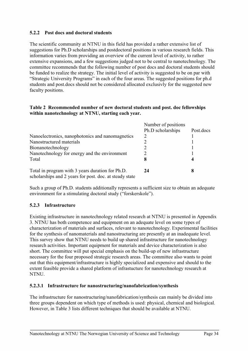
Nanotechnology at NTNU The Norwegian University of Science and Technology Page 34
5.2.2 Post docs and doctoral students
The scientific community at NTNU in this field has provided a rather extensive list ofsuggestions for Ph.D scholarships and postdoctoral positions in various research fields. Thisinformation varies from providing an overview of the current level of activity, to ratherextensive expansions, and a few suggestions judged not to be central to nanotechnology. Thecommittee recommends that the following number of post docs and doctoral students shouldbe funded to realize the strategy. The initial level of activity is suggested to be on par with“Strategic University Programs” in each of the four areas. The suggested positions for ph.dstudents and post.docs should not be considered allocated exclusivly for the suggested newfaculty positions.
Table 2 Recommended number of new doctoral students and post. doc fellowships
within nanotechnology at NTNU, starting each year.
Number of positionsPh.D scholarships Post.docs
Nanoelectronics, nanophotonics and nanomagnetics 2 1Nanostructured materials 2 1Bionanotechnology 2 1Nanotechnology for energy and the environment 2 1Total 8 4
Total in program with 3 years duration for Ph.D.scholarships and 2 years for post. doc. at steady state
24 8
Such a group of Ph.D. students additionally represents a sufficient size to obtain an adequateenvironment for a stimulating doctoral study (“forskerskole”).
5.2.3 Infrastructure
Existing infrastructure in nanotechnology related research at NTNU is presented in Appendix3. NTNU has both competence and equipment on an adequate level on some types ofcharacterization of materials and surfaces, relevant to nanotechnology. Experimental facilitiesfor the synthesis of nanomaterials and nanostructuring are presently at an inadequate level.This survey show that NTNU needs to build up shared infrastructure for nanotechnologyresearch activities. Important equipment for materials and device characterization is alsoshort. The committee will put special emphasis on the build-up of new infrastructurenecessary for the four proposed strategic research areas. The committee also wants to pointout that this equipment/infrastructure is highly specialized and expensive and should to theextent feasible provide a shared platform of infrastucture for nanotechnology research atNTNU.
5.2.3.1 Infrastructure for nanostructuring/nanofabrication/synthesis
The infrastructure for nanostructuring/nanofabrication/synthesis can mainly be divided intothree groups dependent on which type of methods is used: physical, chemical and biological.However, in Table 3 lists different techniques that should be available at NTNU.
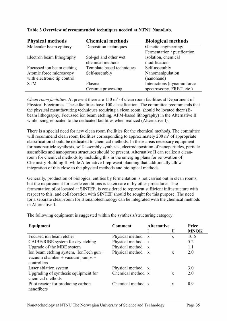
Nanotechnology at NTNU The Norwegian University of Science and Technology Page 35
Table 3 Overview of recommended techniques needed at NTNU NanoLab.
Physical methods Chemical methods Biological methodsMolecular beam epitaxy Deposition techniques Genetic engineering/
Fermentation / purificationElectron beam lithography Sol-gel and other wet
chemical methodsIsolation, chemicalmodification.
Focussed ion beam etching Template based techniques Self-assemblyAtomic force microscopywith electronic tip control
Self-assembly Nanomanipulation(nanohand)
STM PlasmaCeramic processing
Interactions (dynamic forcespectroscopy, FRET, etc.)
Clean room facilities. At present there are 150 m2 of clean room facilities at Department ofPhysical Electronics. These facilities have 100 classification. The committee recommends thatthe physical manufacturing techniques requiring a clean room, should be located there (E-beam lithography, Focussed ion beam etching, AFM-based lithography) in the Alternative IIwhile being relocated to the dedicated facilities when realized (Alternative I).
There is a special need for new clean room facilities for the chemical methods. The committeewill recommend clean room facilities corresponding to approximately 200 m2 of appropriateclassification should be dedicated to chemical methods. In these areas necessary equipmentfor nanoparticle synthesis, self-assembly synthesis, electrodeposition of nanoparticles, particleassemblies and nanoporous structures should be present. Alternative II can realize a clean-room for chemical methods by including this in the emerging plans for renovation ofChemistry Building II, while Alternative I represent planning that additionally allowintegration of this close to the physical methods and biological methods.
Generally, production of biological entities by fermentation is not carried out in clean rooms,but the requirement for sterile conditions is taken care of by other procedures. Thefermentation pilot located at SINTEF, is considered to represent sufficient infrastructure withrespect to this, and collaboration with SINTEF should be sought for this purpose. The needfor a separate clean-room for Bionanotechnology can be integrated with the chemical methodsin Alternative I.
The following equipment is suggested within the synthesis/structuring category:
Equipment Comment Alternative
I IIPrice
MNOK
Focused ion beam etcher Physical method x x 10.6CAIBE/RIBE system for dry etching Physical method x 5.2Upgrade of the MBE system Physical method x 1.1Ion beam etching system, IonTech gun +vacuum chamber + vacuum pumps +controllers
Physical method x x 2.0
Laser ablation system Physical method x 3.0Upgrading of synthesis equipment forchemical methods
Chemical method x x 2.0
Pilot reactor for producing carbonnanofibers
Chemical method x x 0.9

Nanotechnology at NTNU The Norwegian University of Science and Technology Page 36
Preparation facilities for nanoscaleelectrocatalysts
Chemical method x x 1.0
Total, synthesis/structuring 25.8 16.5
AFM/STM - new investments. Since AFM/STM can be considered both as nanostructuringtool as well as characterization tool and the fact that several groups have reported needs forsuch equipment it is treated separately. There are today 2 different ATM and STMinstruments at NTNU (Appendix 3). In addition, there is one in the process of beingpurchased, and one instrument owned by SINTEF. The committee received a rather extensivelist of suggestions in this area. Here it is also important to consider shared facilities exceptwhere installation in clean room, etc. makes common use not recommended. Cross-contamination is another issue that also calls for dedicated set-ups. The committeerecommends the following investments
Equipment Alternative
I IIPrice
MNOK
Atomic force microscope, NanoMan/NanoScope 4 x x 3.2Upgrade AFM x x 2.1Upgrade STEM/AFM x x 1.0
STM, with photoemission x 2.5UHV variable temperature AFM x 6
Total, AFM/STM 14.8 6.3
Infrastructure for characterization. The scanning probe microsopes suggested above arecombined manufacturing and characterization tools. In addition, the following generalequipment for characterization is necessary: Diffraction, electron microscopy, nanoparticlecharacterization, spectroscopy, physical/chemical property characterization.
Equipment Alternative
Diffraction
I IIPrice
MNOK
Up-dating of present x-ray facilities including 4-circle x-ray diffractometer
x x 4.3
LEED (low energy electron diffraction) optics x x 0.4Electron microscopy
Up-grading of existing TEM equipment x 3.1Nanoparticle characterization
Particle size determination from micron down tonanometer range by different methods
x x 3.0
Spectroscopy
Photoemission spectroscopy for current VT-UHV STM x 1.0FTIR-PL lab for carrier lifetime measurements x 0.55Mass-spectrometers including LC/MS x 0.5
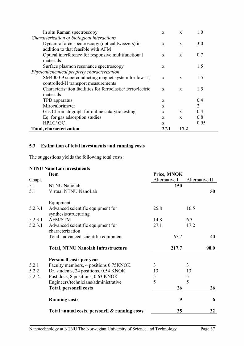
Nanotechnology at NTNU The Norwegian University of Science and Technology Page 37
In situ Raman spectroscopy x x 1.0Characterization of biological interactions
Dynamic force spectroscopy (optical tweezers) inaddition to that feasible with AFM
x x 3.0
Optical interference for responsive multifunctionalmaterials
x x 0.7
Surface plasmon resonance spectroscopy x 1.5Physical/chemical property characterization
SM4000-9 superconducting magnet system for low-T,controlled-H transport measurements
x x 1.5
Characterisation facilities for ferroelastic/ ferroelectricmaterials
x x 1.5
TPD apparatus x 0.4Mirocalorimeter x 2Gas Chromatograph for online catalytic testing x x 0.4Eq. for gas adsorption studies x x 0.8HPLC/ GC x 0.95
Total, characterization 27.1 17.2
5.3 Estimation of total investments and running costs
The suggestions yields the following total costs:
NTNU NanoLab investments
Item Price, MNOK
Chapt. Alternative I Alternative II5.1 NTNU Nanolab 150
5.1 Virtual NTNU NanoLab 50
Equipment5.2.3.1 Advanced scientific equipment for
synthesis/structuring25.8 16.5
5.2.3.1 AFM/STM 14.8 6.35.2.3.1 Advanced scientific equipment for
characterization27.1 17.2
Total, advanced scientific equipment 67.7 40
Total, NTNU Nanolab Infrastructure 217.7 90.0
Personell costs per year
5.2.1 Faculty members, 4 positions 0.75KNOK 3 35.2.2 Dr. students, 24 positions, 0.54 KNOK 13 135.2.2. Post docs, 8 positions, 0.63 KNOK 5 5
Engineers/technicians/administrative 5 5Total, personell costs 26 26
Running costs 9 6
Total annual costs, personell & running costs 35 32

Nanotechnology at NTNU The Norwegian University of Science and Technology Page 38
The equipment needed for nanotechnology research is often very advanced and expensive andskilled persons to maintain and operate the equipment is necessary. To maintain, keep highcompetence and perform high quality experiments we therefore need a qualified staff of 7-8technicians.
5.4 Study program
Providing competence in nanotechnology to the society requires a focus on education andtraining of candidates within this field. The committee therefore proposes to establish a studyprogram at the Master of Science level (“Master i teknologi”) in nanotechnology. Offeringsuch a program would flag a long-term commitment on the part of NTNU in this field, can bepivotal in placing Norway on the nanotechnology scene, and provide the competence requiredfor industrial development of emerging knowledge-based industries in Norway. The latterfacet is considered to be of special importance to Norway (point 3 in mandate) in the contextof transforming the structure of Norwegian industry to be less dependent of raw-materials.
Appendix 2 lists existing courses judged to include a certain element of nanoscience andnanotechnology. Alongside with a strategic choice of NTNU to hire 3-4 new faculty positionswith a clear nanotechnology profile, this could represent a sufficient start-up background for astudy program. A Master of Science study program in nanotechnology, is suggested to beorganized as multidisciplinary 3 year program with enrollment following the initial two yearsof the integrated 5 years, 300 ECTS credit point study programs in Physics and Mathematics,Chemistry- and biotechnology, or Electrical engineering (Fig. 1). Materials technologyrepresents possible fourth channel that should be evaluated as a basis. A model similar to thestudy program in Industrial Ecology at NTNU is proposed.
Year543
Master of science, nanotechnology, 180 ECTS credit points
21
Chemistry- andbiotechnology
Physics andmathematics
ElectricalEngineering
Fig. 1. Structure of suggested master of science study program, nanotechnology
With such an organization, the interface to the study programs with focus on microelectronics,materials technology, chemistry, physics, biophysics and medical technology, can beachieved. A stronger interface with biology can be achieved by selection of topics within the180 ECTS credit study program. The current study programs within Bachelor in NaturalSciences, Biology, are judged not to have a sufficiently strong component within mathematicsand other disciplines. Within this suggested structure, the candidates completing their thesiswithin this study program can keep up a profile reflecting their speciality/backgroundproviding competence for a wider job market.

Nanotechnology at NTNU The Norwegian University of Science and Technology Page 39
This organizational model is different from e.g. the one at Copenhagen University, wherethere is a string of “nanotopics” from the first year of a five-year masters program(http://www.nano.ku.dk/uddannelse/kursusbeskrivelser.htm). The strength of the proposedstructure is that it reflects the multidisciplinary nature of nanotechnology by bringing students(and faculty) with different backgrounds together, and that this can be achieved at areasonable cost.
6 National and international collaborative structures
A candidate for a national collaborative partner within this field was already identified andincluded by the selection Anders Hanneborg at the Norwegian Microtechnology Center, Oslo,as one of the committee members. Additional Norwegian partners to seek collaborativestructures within are SINTEF in more general context, IFE, and the other universities inNorway. Within such a collaborative context, the partners should establish a profile that iscomplementing each other, and seek national collaborations. This could extent to an evenmore ambitious plan by including Alternative I as part of a Norwegian NanotechnologyCenter. This would require committed partnership in an early phase of the project with thefollowing partners: NTNU, University of Oslo, SINTEF and major Norwegian Industries. Aplan for funding of the suggested academic positions and scholarships include a partnershipbetween NTNU, the Norwegian Research Council, and Norwegian industry.
The committee received input from the various research groups on elements on variousresearch networks (Appendix 1 and 4). This represents “bottom-up” examples of establishedconnectivities among research groups within an international collaboration in mind. Inaddition to the focus on the European dimension in the survey, there are numerous possibleoptions in e.g. USA and Japan for collaboration within this field. Most important on theinternational collaborative scene is that NTNU in the long term develop high quality,nanotechnology training and research both as a basis for being attractive partners and as abasis for development of new industry.