new from characterization strategies to pdk & eda tools for … · 2017. 12. 15. · dr. lluís...
TRANSCRIPT
Departament de Microelectrònica i Sistemes Electrònics
From characterization
strategies to PDK & EDA
Tools for Printed
Electronics
Francesc Vila Garcia
Memòria de Tesipresentada per optar al títol de
Doctor en Microelectrònica i Sistemes
Electrònics
Setembre 2015


Dr. Lluís Terés Terés, Científico Titular del Consejo Superior de InvestigacionesCientíficas i Professor Associat del Departament de Microelectrònica i SistemesElectrònics,
Certifica
que la Memòria de Tesi From characterization strategies to PDK & EDA Toolsfor Printed Electronics presentada per Francesc Vila Garcia per optar al títolde Doctor en Microelectrònica i Sistemes Electrònics s’ha realitzat sota la sevadirecció a l’Institut de Microelectrònica de Barcelona pertanyent al Centro Nacionalde Microelectrónica del Consejo Superior de Investigaciones Científicas i ha estattutoritzada en el Departament de Microelectrònica i Sistemes Electrònics de laUniversitat Autònoma de Barcelona.
Director Dr. Lluís Terés Terés . . . . . . . . . . . . . . . . . . . . . . . . . . . . . . . .
. . . . . . . . . . . . . . . . . . . . . . . . . , a . . . . . . de . . . . . . . . . . . . . . . . de . . . . . . . . .


If we knew what it was that we were doing,it would not be called research, would it?
– Albert Einstein
v

ResumDurant els últims anys, les tecnologies d’electrònica impresa (PE) estan atraientmolta atenció, principalment degut a que es poden fabricar grans àrees, i sónuna alternativa de baix cost a la microelectrònica tradicional. D’entre totes lestecnologies disponibles, la fabricació emprant impresores d’injecció de tinta (inkjet)resulta particularment interessant, al ser un mètode d’impressió digital (reduint elsresidus generats al fabricar), i no tenir contacte amb el substrat (per tant permetla utilització de molts tipus diferents de substrats).
La tecnologia inkjet encara està patint un gran desenvolupament, cosa que fa difícilque es puguin dissenyar circuits i sistemes sense tenir un gran coneixement sobreels processos que hi ha al darrere. A més a més, la mancança d’eines específicamentdissenyades per a inkjet crea un gran distància entre els dissenyadors i els tecnòlecsresponsables de desenvolupar la tecnologia, dificultant així una adopció generalitzadade la tecnologia inkjet.
Aquesta tèsi contribueix a apropar els dissenyadors a la tecnologia, proposanti adaptant fluxes i kits de disseny existents i basats en microelectrònica, a lestecnologies inkjet, complementant-los amb eines específiques per adaptar-los a lespeculiaritats de l’inkjet. D’aquesta manera aconseguim un camí directe des deldisseny a la fabricació, abstraient els detalls tecnològics del disseny.
A més a més, per tancar el camí entre disseny i la fabricació, aquesta tèsi proposaun entorn semi-automàtic de caracterització, que es fa servir per analitzar elcomportament de la tinta dipositada, inferint quines correccions són necessàriesper a què el resultat fabricat correspongui tant com sigui possible al disseny. Elconeixement extret d’aquest pas s’incorporarà en una eina EDA específica queanalitza i aplica automàticament les correccions extretes a un disseny.
vii

AbstractDuring last years, Printed Electronics technologies have attracted a great deal ofattention due to being a low-cost, large area electronics manufacturing process.From all available technologies, inkjet printing is of special interest, because ofits digital nature, which reduces material waste; and being a non-contact process,which allows printing on a great variety of substrates.
Inkjet printing is still on heavy development, thus making designing for it difficultwithout an in-depth knowledge of how the manufacturing process works. In addition,currently there is a lack of specific tools aiding to design for it, creating a large gapbetween designers and technology developers and difficulting a wide adoption ofthis particular technologies.
The work presented on this thesis contributes to bridge the existing gap be-tween designers and technology developers by proposing and adapting existingmicroelectronics-based design flows and kits, while complementing them with cus-tom, PE specific Electronic Design Automation tools; to achieve a direct path fromdesign to manufacturing, and abstract technology specific details from the designstages. This is achieved by combining a design flow with a PE Process/PhysicalDesign Kit, and a set of EDA tools adapted to PE.
In addition, to finally bridge design and manufacturing, this thesis proposes a semi-automated characterization methodology, used to analyze the deposited ink behavior,and infer all necessary corrections needed to ensure that the final fabricated resultcorresponds as much as possible to the intended design. This knowledge is thenintegrated into an specific EDA framework which will perform the aformentionedcorrections automatically.
viii

Acknowledgements
Firstly, I would like to express my sincere gratitude to my advisor, Dr. Luís TerésTerés, for continuous support of my PhD study and related research. His guidancehelped me in all the time of the research and writing of this thesis. In addition, Iwould like to thank Dr. Jordi Carrabina, for his insightful comments and, togetherwith Lluís, giving me the oportunity to work in this thesis.
Besides, I would also like to thank my colleagues at ICAS, specially Jofre Pallarès,for his great support and knowledge, giving advice and guiding on the difficult partsof this research. Thanks all for the great time spent working on IMB. Special thanksalso to Eloi, Carme, Adrià, and all the people working in the TDK4PE project. Ithas been a pleasure to work with you in this great and ambicious project, allowingme to learn from you. Special thanks for Arjen, Niels, Remco(s), and Jan, fromPhoeniX for allowing me to do a short stay in Enschede, giving me the oportunityto work with you after this thesis, and starting a new exciting adventure.
In addition, I would like to thank my former university classmates, some stillremaining in the university pursuing their PhD’s. Thank you very much to AlbertSaa and Xicola, Ferran, Toni, Miguel, Arturo. Thanks for the discussions duringlunch, the everyday “creative Friday”, and all of your support. You have helpedme to deal with the pressure of doing a PhD, and provided me with very usefuldirections on topics that I was not familiar with.
My sincere thanks to Ricardo, Salva, and Ciscu, my flatmates during all of theseyears. It has been a pleasure living with you, enjoying great times and discussions.
In this agreements I cannot forget to thank Cristina, Jordi, Mònica, Mimar, and
ix

all of my friends from Lloret. You have been a huge support during this time, andhelped me on my most tough moments. A huge and most sincere thank you.
Last but not least, I want to thank my family, specially my parents. Without theirsupport and education I would not be on the place I am today. Thanks for all theeffort and for giving me the oportunity to pursue, first an Engineering bachelor,and then my PhD.
x

Contents
1 Introduction 1
1.1 PE Technologies . . . . . . . . . . . . . . . . . . . . . . . . . . . . . 1
1.2 State of the art and motivation . . . . . . . . . . . . . . . . . . . . . 3
1.3 Thesis context . . . . . . . . . . . . . . . . . . . . . . . . . . . . . . 7
1.4 Aims and objectives . . . . . . . . . . . . . . . . . . . . . . . . . . . 8
2 Design Flows, Tools and Kits 11
2.1 Abstraction levels and design flows . . . . . . . . . . . . . . . . . . . 11
2.2 PE design flows . . . . . . . . . . . . . . . . . . . . . . . . . . . . . . 13
2.3 Process Design Kits . . . . . . . . . . . . . . . . . . . . . . . . . . . 15
2.3.1 Necessary process information . . . . . . . . . . . . . . . . . . 16
2.3.2 XML interface . . . . . . . . . . . . . . . . . . . . . . . . . . 17
2.4 Characterization strategies and setup . . . . . . . . . . . . . . . . . . 18
2.5 Conclusions . . . . . . . . . . . . . . . . . . . . . . . . . . . . . . . . 19
3 Specific Design Kits and EDA tools for PE 21
xi
3.1 EDA tools selection . . . . . . . . . . . . . . . . . . . . . . . . . . . 21
3.1.1 FOSS tool set . . . . . . . . . . . . . . . . . . . . . . . . . . . 22
3.1.2 Commercial tools . . . . . . . . . . . . . . . . . . . . . . . . . 26
3.2 EDA tool customizations . . . . . . . . . . . . . . . . . . . . . . . . 26
3.2.1 Free/Open source tool selection . . . . . . . . . . . . . . . . . 26
3.2.2 Commercial package . . . . . . . . . . . . . . . . . . . . . . . 30
3.3 XML database . . . . . . . . . . . . . . . . . . . . . . . . . . . . . . 30
3.3.1 XML representation . . . . . . . . . . . . . . . . . . . . . . . 30
3.3.2 FOSS tool set . . . . . . . . . . . . . . . . . . . . . . . . . . . 41
3.3.3 Commercial tool set . . . . . . . . . . . . . . . . . . . . . . . 46
3.4 Conclusions . . . . . . . . . . . . . . . . . . . . . . . . . . . . . . . . 52
4 Image based technology characterization 55
4.1 Experimental approach . . . . . . . . . . . . . . . . . . . . . . . . . . 55
4.1.1 Experiment generation . . . . . . . . . . . . . . . . . . . . . . 56
4.2 Analysis . . . . . . . . . . . . . . . . . . . . . . . . . . . . . . . . . . 63
4.2.1 Image processing operations . . . . . . . . . . . . . . . . . . . 63
4.2.2 Misalignment . . . . . . . . . . . . . . . . . . . . . . . . . . . 68
4.2.3 Score calculation . . . . . . . . . . . . . . . . . . . . . . . . . 71
4.2.4 Statistical procedures . . . . . . . . . . . . . . . . . . . . . . 74
4.2.5 Electrical tests . . . . . . . . . . . . . . . . . . . . . . . . . . 80
4.3 Conclusions . . . . . . . . . . . . . . . . . . . . . . . . . . . . . . . . 85
5 Automatic Compensations 89
5.1 Layout2Bitmap . . . . . . . . . . . . . . . . . . . . . . . . . . . . . . 89
5.1.1 Tool description . . . . . . . . . . . . . . . . . . . . . . . . . 89
5.1.2 Design loading . . . . . . . . . . . . . . . . . . . . . . . . . . 90
5.1.3 Design compensation . . . . . . . . . . . . . . . . . . . . . . . 91
xii

5.2 Layout2Bitmap into design flows . . . . . . . . . . . . . . . . . . . . 102
5.2.1 Free/OSS flow integration: Glade . . . . . . . . . . . . . . . . 104
5.2.2 Commercial flow integration: MaskEngineer . . . . . . . . . . 104
5.3 Results and conclusions . . . . . . . . . . . . . . . . . . . . . . . . . 105
6 Global conclusions and further activities 109
xiii

List of Figures
1.1 Inkjet printing printhead diagram. . . . . . . . . . . . . . . . . . . . 3
1.2 Different printing imperfections. . . . . . . . . . . . . . . . . . . . . . 4
1.3 OpenPDK use cases. . . . . . . . . . . . . . . . . . . . . . . . . . . . 6
2.1 Evolution of technology and design abstraction levels. . . . . . . . . 12
2.2 Diagram of the proposed design flow for PE. . . . . . . . . . . . . . 14
2.3 PDK development and characterization, and EDA customization loop. 15
2.4 PDK diagram with an abstraction layer. . . . . . . . . . . . . . . . . 17
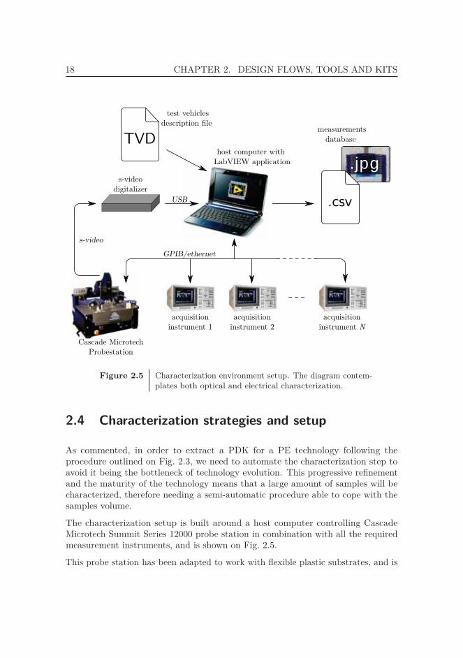
2.5 Characterization environment setup. The diagram contemplates bothoptical and electrical characterization. . . . . . . . . . . . . . . . . . 18
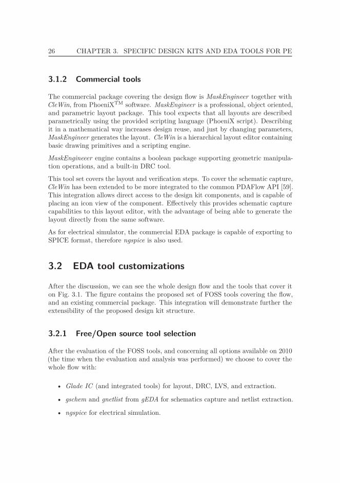
3.1 Complete design flow, containing all used tools and intermediateformats. The diagram contains both the FOSS and the commercialflow. This diagram can be seen as a detailed version of Fig. 2.2 . . . 27
3.2 General information and manipulation strategy. For each part, theproposed file formats are shown. . . . . . . . . . . . . . . . . . . . . 31
3.3 Fundamental set of design rules and basic manipulation operations. . 36
xv

3.4 Sample of complex design rules defined combining several layers. . . 37
3.5 XML usage strategies. Shows direct usage by the tools or usage viacustom converter. . . . . . . . . . . . . . . . . . . . . . . . . . . . . . 42
3.6 Glade customizations. . . . . . . . . . . . . . . . . . . . . . . . . . . 45
3.7 Comparison of the integrated model in ngspice and actual devicecharacterization measurements. . . . . . . . . . . . . . . . . . . . . . 46
3.8 PDK generation for PDAFlow API tools. The arrows represent theinformation flow. Dashed lines represent the added implementationinto PDA API code. . . . . . . . . . . . . . . . . . . . . . . . . . . . 47
3.9 MaskEngineer cross-section/layer mapping philosophy, w is the shapewidth. The layer names/colors come from the TDK4PE technology. 48
3.10 Result of loading the design kit into MaskEngineer, and the resultingtechnology layers. . . . . . . . . . . . . . . . . . . . . . . . . . . . . . 49
4.1 General flow diagram of characterization procedure. This diagramcontemplates both optical and electrical characterization. . . . . . . 57
4.2 Generated experiment layout. The resulting design comprises 1) thesubstrate alignment marks, 2) the camera alignment structure, and3) the experiment samples. . . . . . . . . . . . . . . . . . . . . . . . 58
4.3 Set of different test structures with their parameters. . . . . . . . . . 61
4.4 Set of compensations applied to a L test structure. The Nonecorresponds to the control group. . . . . . . . . . . . . . . . . . . . . 62
4.5 Example of morphological operations using a disk of radius r as astructuring element. The light gray shaded region is the originalshape, the black is the structuring element, and the medium gray isthe resulting shape. . . . . . . . . . . . . . . . . . . . . . . . . . . . . 65
4.6 Different heuristics for connected components labelling. . . . . . . . 66
4.7 Results of the cleaning process step by performed operations: a) cap-tured image, b) after thresholding, and opening/closing, and d) aftersmall features removal. . . . . . . . . . . . . . . . . . . . . . . . . . . 67
4.8 a) Removed map of a whole DIN A5 foil. The printing direction isindicated by the white arrows (right to left and top to bottom), b)Mean values across the x axis, and c) Autocorrelation plot. . . . . . 67
xvi
4.9 Example of image misalignment. On the cross-correlation contourplot, the maximum is marked with a black × (central dot on (c)). . 69
4.10 Misalignment across a whole DIN A5 foil. The vector streamlinesindicate the substrate dilation directions, and the color the amount. 70
4.11 Resulting distance map transform on the regions of interest. . . . . . 72
4.12 Score median depending on test template extension. The diagramshows the drop placement with the appropriate measurements. . . . 73
4.13 Initial data distribution and profile log-Likelihood for Box-Cox trans-form. Note: The shaded regions correspond to σ, 2σ, and 3σ intervals. 76
4.14 General distribution of transformed score results. . . . . . . . . . . . 77
4.15 Initial estimated means and prediction intervals for outlier filtering . 78
4.16 Prediction intervals and filtered new foil data. . . . . . . . . . . . . . 79
4.17 Tukey HSD post-hoc test results. . . . . . . . . . . . . . . . . . . . . 80
4.18 Comparison of the same structure with different compensations. . . 81
4.19 OTFT structure as designed and resulting cross-section. Blue partsare the source and drain electrodes, red is the gate. The channelforms between fingers. . . . . . . . . . . . . . . . . . . . . . . . . . . 82
4.20 Electrical test results of the finger structures. The separation is notthe actual designed separation, but the effective separation accountingto ink spreading. . . . . . . . . . . . . . . . . . . . . . . . . . . . . . 83
4.21 Resulting finger structures without and with compensation. . . . . . 85
4.22 3D interferometer profile and finger section cut for a compensatedfingered structure. The three cuts correspond to different positionsinside the structure. . . . . . . . . . . . . . . . . . . . . . . . . . . . 86
5.1 Available primitive element types defined in GDS specification. . . . 92
5.2 Representation of the two available polygon boundaries. . . . . . . . 93
5.3 Representation of the two available polygon boundaries. . . . . . . . 93
5.4 Polygon with holes example. . . . . . . . . . . . . . . . . . . . . . . . 94
5.5 Regularized set of boolean operations on polygons. . . . . . . . . . . 95
5.6 Sweep line approach to segment intersections. . . . . . . . . . . . . . 96
xvii

5.7 Overlay of two planar subdivisions. . . . . . . . . . . . . . . . . . . . 97
5.8 Polygon offsetting examples. The shaded region corresponds to theamount offseted (δ1 for exterior offset, δ2 for interior offset). . . . . . 98
5.9 Winding number calculation for region containing point q. Theresulting number is the same regarding which ray is shot. . . . . . . 99
5.10 Offset curves calculation. The shaded region corresponds to the finalcalculated shape. . . . . . . . . . . . . . . . . . . . . . . . . . . . . . 100
5.11 Pattern matrix definition and resulting drop positions on the grid. . 101
5.12 Sweep line fill procedure. The shaded area is already filled, and thered highlighted scanline is the active region. . . . . . . . . . . . . . . 102
5.13 Flow diagram of the general L2B operation. . . . . . . . . . . . . . . 103
5.14 General structure of the L2B framework. . . . . . . . . . . . . . . . 104
5.15 Schematic to generated bitmaps process: a) symbol, b) schematic, c)layout, d) set of generated bitmaps, and e) close view on performedcompensations. Layout2Bitmap processes the layout on c) to generatea set of masks on d). . . . . . . . . . . . . . . . . . . . . . . . . . . . 107
xviii

List of Tables
3.1 Summary of the main characteristics for each layout editor evaluated. 23
3.2 Summary of the main characteristics for each schematic captureprogram evaluated. . . . . . . . . . . . . . . . . . . . . . . . . . . . . 24
3.3 Summary of the main characteristics for each electrical simulatorprogram evaluated. . . . . . . . . . . . . . . . . . . . . . . . . . . . . 25
4.1 Different image region identifiers. . . . . . . . . . . . . . . . . . . . . 71
4.2 Measures of skewness and kurtosis of log(Sp) for different compensa-tions. It approximates the normal distribution values (γ1 = 0, γ2 = 3) 76
4.3 Approximated α = 0.95 confidence intervals for proportion of workingfingers. . . . . . . . . . . . . . . . . . . . . . . . . . . . . . . . . . . . 84
xix


List of Listings
3.1 Excerpt of the layer XSD definition. . . . . . . . . . . . . . . . . . . 32
3.2 Excerpt of the layer XML definition . . . . . . . . . . . . . . . . . . 33
3.3 Excerpt of the operation defintion schema. . . . . . . . . . . . . . . 33
3.4 Example of operation definition in the XML database. . . . . . . . . 34
3.5 DRC rule definition schema. . . . . . . . . . . . . . . . . . . . . . . 34
3.6 DRC rule definition rule definition. . . . . . . . . . . . . . . . . . . 35
3.7 Device model schema definition. . . . . . . . . . . . . . . . . . . . . 38
3.8 Device model XML contents. . . . . . . . . . . . . . . . . . . . . . . 39
3.9 Device model SPICE include line. . . . . . . . . . . . . . . . . . . . 39
3.10 Compensation operations schema. . . . . . . . . . . . . . . . . . . . 40
3.11 Compensation operation XML contents. . . . . . . . . . . . . . . . 41
3.12 Layers in Glade IC technology file format. . . . . . . . . . . . . . . 43
3.13 Design Rule Check (DRC) values autogenerated file. . . . . . . . . . 44
3.14 DRC script. . . . . . . . . . . . . . . . . . . . . . . . . . . . . . . . 44
3.15 Example of PDAFlow technology base class. . . . . . . . . . . . . . 50
xxi

3.16 Example of PDAFlow technology base class. . . . . . . . . . . . . . 50
3.17 Example of inverter design and SPICE simulation. . . . . . . . . . . 51
3.18 Example of inverter code with Layout2Bitmap export. . . . . . . . . 52
4.1 Generation script extract. . . . . . . . . . . . . . . . . . . . . . . . . 60
4.2 General PCell structure. . . . . . . . . . . . . . . . . . . . . . . . . . 61
5.1 Full listing of the export function inside the design kit definition forPDAFlow design kits, and its usage. . . . . . . . . . . . . . . . . . . 105
xxii

Publication list
This thesis is based in part on (and led to) the following published articles andconferences:
[1] Francesc Vila et al. Layout to bitmap: A layout design compensator and bitmapconverter for Printed Electronics. In LOPE-C. 2011.
[2] Eloi Ramon et al. Inkjet printed electronics at uab-cnm: Technology anddesign flow developments. In Proceedings of the 38th International researchconference of iarigai. The International Association of Research Organizationsfor the Information, Media and Graphic Arts Industries, Buadpest, Hungary,September 2011. ISBN 978-3-9812704-4-0.
[3] Jofre Pallarès et al. PE TDK Development Methodology: a nexus betweenTechnology & Design. In ECME. 2011.
[4] Francesc Vila et al. A complete suite of open/free EDA tools for PE physicaldesign. In Design, Automation and Test in Europe. 2013.
[5] Francesc Vila et al. PDK development for Printed/Organic Electronics based onXML. In DCIS’2013: XXVIII Conference on Design of Circuits and IntegratedSystems. 2013.
[6] Francesc Vila et al. Physical design flow for Printed Electronics based onopen/free EDA tools. In International Conference on Organic Electronics(ICOE). 2013.
xxiii

[7] Francesc Vila et al. A complete suite of open/free EDA tools for PE physicaldesign. In Design, Automation and Test in Europe. 2013.
[8] Jordi Carrabina et al. Design rules checking for printing electronic devices:concept, generation and usage. In IARIGAI Conference. 2013.
[9] Stepan Sutula et al. Teaching Mixed-Mode Full-Custom VLSI Design withgaf, SpiceOpus and Glade. In Proceedings of the 10th European Workshop onMicroelectronics Education (EWME). 2014.
[10] Jofre Pallarès et al. A freeware eda framework for teaching mixed-mode full-custom vlsi design. In Proceedings of the XXIX Conference on Design ofCircuits and Integrated Systems. DCIS, Madrid, Spain, November 2014.
[11] Francesc Vila and Jofre Pallarès. CSEM_Tech1 Design Tutorial, June 2014.
[12] Francesc Vila et al. Semi-automatic PE Technology & Device Library Charac-terization for PDK Development. In Large-area, Organic, & Printed ElectronicsConvention (LOPEC). 2014.
[13] Francesc Vila et al. A fully-automated methodology and system for printedelectronics foil characterization. In Microelectronic Test Structures (ICMTS),2015 International Conference on, pages 188–192. March 2015. ISSN 1071-9032.doi:10.1109/ICMTS.2015.7106138.
[14] Francesc Vila et al. A systematic study of pattern compensation methods for all-inkjet functional printing processes. Components, Packaging and ManufacturingTechnology, IEEE Transactions on. Accepted. Pending revisions.
xxiv

List of Acronyms
ASPEC-TDK Application Specific Printed Electronic Circuits - Technology De-sign Kits . . . . . . . . . . . . . . . . . . . . . . . . . . . . . . . . . . . . . . . . . . . . . . . . . . . . . . . . . . . . . . . . . 7
API Application Programming Interface . . . . . . . . . . . . . . . . . . . . . . . . . . . . . . . . . . . . . . . 7
ASIC Application Specific Integrated Circuit . . . . . . . . . . . . . . . . . . . . . . . . . . . . . . . . . 13
CAD Computer Aided Design . . . . . . . . . . . . . . . . . . . . . . . . . . . . . . . . . . . . . . . . . . . . . . . . 15
CAM Computer Aided Manufacturing . . . . . . . . . . . . . . . . . . . . . . . . . . . . . . . . . . . . . . . 97
CIF Caltech Intermediate Format
CIJ Continous Inkjet . . . . . . . . . . . . . . . . . . . . . . . . . . . . . . . . . . . . . . . . . . . . . . . . . . . . . . . . . . 2
CSV Comma-Separated Values . . . . . . . . . . . . . . . . . . . . . . . . . . . . . . . . . . . . . . . . . . . . . . . 19
DLL Dynamic-link Library . . . . . . . . . . . . . . . . . . . . . . . . . . . . . . . . . . . . . . . . . . . . . . . . . . . 47
xxv

DoD Drop on Demand . . . . . . . . . . . . . . . . . . . . . . . . . . . . . . . . . . . . . . . . . . . . . . . . . . . . . . . . 2
DRC Design Rule Check . . . . . . . . . . . . . . . . . . . . . . . . . . . . . . . . . . . . . . . . . . . . . . . . . . . . xxi
DT Distance Transform . . . . . . . . . . . . . . . . . . . . . . . . . . . . . . . . . . . . . . . . . . . . . . . . . . . . . . 71
DXF Drawing Interchange Format . . . . . . . . . . . . . . . . . . . . . . . . . . . . . . . . . . . . . . . . . . 100
EDA Electronic Design Automation . . . . . . . . . . . . . . . . . . . . . . . . . . . . . . . . . . . . . . . . . . . 5
ERC Electrical Rule Check. . . . . . . . . . . . . . . . . . . . . . . . . . . . . . . . . . . . . . . . . . . . . . . . . . .13
FEC Fluidic Effects Correction . . . . . . . . . . . . . . . . . . . . . . . . . . . . . . . . . . . . . . . . . . . . . . . . 8
FOSS Free/Open Source Software . . . . . . . . . . . . . . . . . . . . . . . . . . . . . . . . . . . . . . . . . . . . 22
GDS Graphic Database System . . . . . . . . . . . . . . . . . . . . . . . . . . . . . . . . . . . . . . . . . . . . . . 34
GUI Graphical User Interface . . . . . . . . . . . . . . . . . . . . . . . . . . . . . . . . . . . . . . . . . . . . . . . 104
HDL Hardware Description Language . . . . . . . . . . . . . . . . . . . . . . . . . . . . . . . . . . . . . . . . 12
ILT Inverse Lithography Technology. . . . . . . . . . . . . . . . . . . . . . . . . . . . . . . . . . . . . . . . . .13
IoT Internet of Things . . . . . . . . . . . . . . . . . . . . . . . . . . . . . . . . . . . . . . . . . . . . . . . . . . . . . . . . 1
IP Intellectual Property . . . . . . . . . . . . . . . . . . . . . . . . . . . . . . . . . . . . . . . . . . . . . . . . . . . . . . 11
LVS Layout Versus Schematic . . . . . . . . . . . . . . . . . . . . . . . . . . . . . . . . . . . . . . . . . . . . . . . . . 8
MCS Mask Cross Sections . . . . . . . . . . . . . . . . . . . . . . . . . . . . . . . . . . . . . . . . . . . . . . . . . . . 47
xxvi
MLE Maximum Likelihood Estimator . . . . . . . . . . . . . . . . . . . . . . . . . . . . . . . . . . . . . . . . 75
OASIS Open Artwork System Interchange Standard . . . . . . . . . . . . . . . . . . . . . . . . . 90
OE Organic Electronics. . . . . . . . . . . . . . . . . . . . . . . . . . . . . . . . . . . . . . . . . . . . . . . . . . . . . . . .1
OPC Optical Proximity Correction . . . . . . . . . . . . . . . . . . . . . . . . . . . . . . . . . . . . . . . . . . . 13
OTFT Organic Thin Film Transistor . . . . . . . . . . . . . . . . . . . . . . . . . . . . . . . . . . . . . . . . . 80
PCB Printed Circuit Board . . . . . . . . . . . . . . . . . . . . . . . . . . . . . . . . . . . . . . . . . . . . . . . . . . 13
PCell Parameterizable Cell . . . . . . . . . . . . . . . . . . . . . . . . . . . . . . . . . . . . . . . . . . . . . . . . . . . . 9
PDF Portable Document Format . . . . . . . . . . . . . . . . . . . . . . . . . . . . . . . . . . . . . . . . . . . . . 39
PDK Process/Physical Design Kit. . . . . . . . . . . . . . . . . . . . . . . . . . . . . . . . . . . . . . . . . . . . .5
PE Printed Electronics . . . . . . . . . . . . . . . . . . . . . . . . . . . . . . . . . . . . . . . . . . . . . . . . . . . . . . . . 1
RET Resolution Enhancement Techniques . . . . . . . . . . . . . . . . . . . . . . . . . . . . . . . . . . . .13
SO Shared Object . . . . . . . . . . . . . . . . . . . . . . . . . . . . . . . . . . . . . . . . . . . . . . . . . . . . . . . . . . . . 47
TDK4PE Technology and Design Kits for Printed Electronics . . . . . . . . . . . . . . . . . 7
TVD Test Vehicle Description. . . . . . . . . . . . . . . . . . . . . . . . . . . . . . . . . . . . . . . . . . . . . . . .19
XML eXtensible Markup Language. . . . . . . . . . . . . . . . . . . . . . . . . . . . . . . . . . . . . . . . . . . .5
XPath XML Path Language . . . . . . . . . . . . . . . . . . . . . . . . . . . . . . . . . . . . . . . . . . . . . . . . . 42
xxvii

XSD XML Schema Definition . . . . . . . . . . . . . . . . . . . . . . . . . . . . . . . . . . . . . . . . . . . . . . . . 32
XSL eXtensible Stylesheet Language . . . . . . . . . . . . . . . . . . . . . . . . . . . . . . . . . . . . . . . . . 41
XSL-FO XSL Formatting Objects. . . . . . . . . . . . . . . . . . . . . . . . . . . . . . . . . . . . . . . . . . . .42
XSLT XSL Transformations. . . . . . . . . . . . . . . . . . . . . . . . . . . . . . . . . . . . . . . . . . . . . . . . . .42
xxviii

Introduction 1
Nowadays there is an increasing interest in the field of Organic Electronics (OE)and Printed Electronics (PE), in order to have low-cost, flexible and large areaelectronics for several consumer applications [1], such as wearable technologies andhealthcare applications [2, 3], Internet of Things (IoT) applications [4], energyharvesting and storage [5, 6], or lighting [7].
The preference for PE over traditional silicon-based microelectronics in this area isdue to the necessity of having large area, thin, and flexible systems, characteristicswhich PE excels in. In addition to this advantages, PE gives a dramatic reductionon production costs, because both the equipment and the materials used are severalorders of magnitude cheaper than the ones used in silicon-based microelectronics.The use of organic materials makes it more environmental friendly.
For these reasons, this research tries to push forward the evolution of these tech-nologies by providing characterization and correction procedures to aid the movefrom design to manufacturing, and making it more accessible to designers comingfrom the electronic world by bridging the gap between design and technology.
1.1 PE Technologies
PE (or Plastic Electronics, Organic Electronics, or Flexible Electronics) is a termthat comprises a set of different printing technologies which are used to produceelectrical circuits by creating electronic devices and systems by depositing inorganicand organic functional inks, usually on plastic and paper substrates. This allowsthe fabrication of electronic components, such as resistors, capacitors, diodes, ortransistors.
The printing techniques are based on the ones used on the graphics industry, and
1

2 CHAPTER 1. INTRODUCTION
nearly all industrial printing methods can be used for PE: screen printing, gravure,flexography, inkjet printing, etc. The manufacturing approach is also similar toconventional printing, because the circuits are fabricated on a layer-by-layer basis,depositing them one on top of the other.
Despite the similarities, the requirements for each domain are very different. Onconventional printing, the maximum resolution is determined by the human eye,but for electronic device manufacturing higher resolutions are desirable. Speciallyfor transistor devices, whose lower dimensions usually imply higher performances.
From all printing techniques, inkjet printing is postulated as one of the morepromising. This technique is a digital, mask-less, low-cost, non-contact depositionmethod. Being an additive process (only depositing material on specified areas)reduces material waste, and makes inkjet printing a more environmental friendlytechnique. In addition, its digital mask-less nature makes inkjet printing a greatprototyping tool, allowing an easy printing pattern customization.
There are two main approaches on inkjet printing: Drop on Demand (DoD) printers,and Continous Inkjet (CIJ) printers [8]. On CIJ printers, there is a continous streamof ink stimulated to break it in drops, which are deflected as necessary to form therequired pattern. DoD printers on the other hand form the drops as needed. DoDprinters have typically more resolution, and can eject smaller droplets than CIJprinters, although the later usually are capable of higher printing speeds.
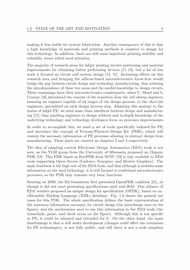
Looking at DoD printers, the ejection mechanism is accomplished mainly by twodifferent technologies: thermal-bubble jets, and piezoelectric jets [9]. Thermal-bubble nozzles achieve ejection by applying an electrical current through a heatingelement. This causes a vaporization of the ink in the reservoir, making a bubbleand a large pressure increase, which ejects a droplet. These nozzles have a lowfabrication cost, and are not affected on air trapped on the ink chamber. On theother hand, the ink needs to resist this rapid thermal change, making it unsuitablefor the deposition of organic materials or materials with low curing temperatures(the nozzle usually heats up to 400 ◦C, while most inks have a curing temperaturearound 150 ◦C).
Piezoelectric nozzles do not apply a thermal load to the ink in order to ejecta droplet and have longer lifespans. Fig. 1.1 contains the basic diagram of apiezoelectric nozzle system. The nozzle ejects the droplets by applying an electricaldriving signal to a piezoelectric transducer. The application of a waveform on thetransducers creates pressure differences on the nozzle chamber, making it to eject anink droplet [10]. This ejection methodology is the preferred method for depositionof functional materials for PE, as it does not create thermal stress to the ink. Inaddition it can eject faster than the thermal nozzles because it does not require thecooling down step of the heating element.
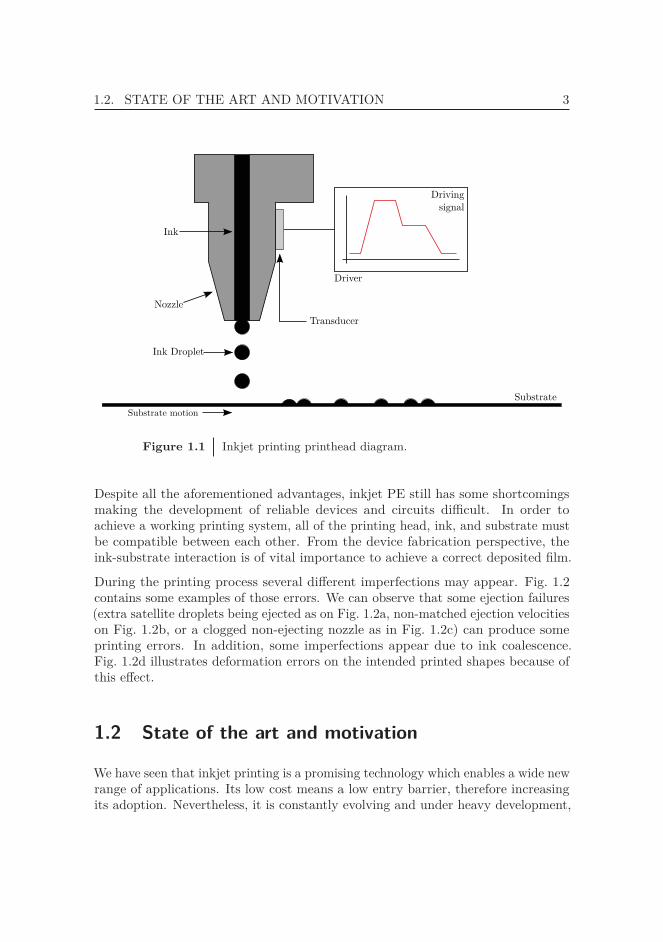
1.2. STATE OF THE ART AND MOTIVATION 3
Driver
Substrate
Drivingsignal
Ink
Nozzle
Ink Droplet
Transducer
Substrate motion
Figure 1.1 Inkjet printing printhead diagram.
Despite all the aforementioned advantages, inkjet PE still has some shortcomingsmaking the development of reliable devices and circuits difficult. In order toachieve a working printing system, all of the printing head, ink, and substrate mustbe compatible between each other. From the device fabrication perspective, theink-substrate interaction is of vital importance to achieve a correct deposited film.
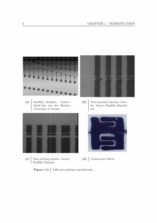
During the printing process several different imperfections may appear. Fig. 1.2contains some examples of those errors. We can observe that some ejection failures(extra satellite droplets being ejected as on Fig. 1.2a, non-matched ejection velocitieson Fig. 1.2b, or a clogged non-ejecting nozzle as in Fig. 1.2c) can produce someprinting errors. In addition, some imperfections appear due to ink coalescence.Fig. 1.2d illustrates deformation errors on the intended printed shapes because ofthis effect.
1.2 State of the art and motivation
We have seen that inkjet printing is a promising technology which enables a wide newrange of applications. Its low cost means a low entry barrier, therefore increasingits adoption. Nevertheless, it is constantly evolving and under heavy development,
4 CHAPTER 1. INTRODUCTION
(a) Satellite droplets. Source:Mark-Jan van der Meulen.University of Twente.
(b) Non-matched ejection veloc-ity. Source Fujifilm DimatixInc.
(c) Non ejecting nozzles. SourceFujifilm Dimatix.
(d) Coalescence effects.
Figure 1.2 Different printing imperfections.
1.2. STATE OF THE ART AND MOTIVATION 5
making it less stable for system fabrication. Another consequence of this is thata high knowledge of materials and printing methods is required to design forthis technology. In addition, there are still some important printing stability andreliability issues which need attention.
The majority of research areas for inkjet printing involve patterning and materialimprovements for obtaining better performing devices [11–13], but a lot of lesswork is focused on circuit and system design [14, 15]. Increasing efforts on thisresearch area and bringing the sillicon-based microelectronics know-how wouldbridge the gap between circuit design and technology manufacturing, thus reducingthe interdependence of these two areas and the needed knowledge to design circuits.These reasonings have their microelectronics counterparts, when C. Mead and L.Conway [16] introduced the concept of the transition from the tall-skinny engineers,meaning an engineer capable of all stages of the design process, to the short-fatengineers, specialized on each design process step. Adapting this analogy to thestatus of inkjet PE, we need some clean interfaces between design and manufactur-ing [17], thus enabling engineers to design without and in-depth knowledge of theunderlying technology, and technology developers focus on processes improvements.
In order to accomplish this, we need a set of tools specifically tailored for PE,and introduce the concept of Process/Physical Design Kit (PDK), which willcontain the necessary information of PE processes allowing to abstract design frommanufacturing. These parts are covered on chapters 2 and 3 respectively.
The idea of adapting current Electronic Design Automation (EDA) tools is notnew, as the VLSI group from the University of Minessota proposed an OrganicPDK [18]. This PDK based on FreePDK from NCSU [19] is only available to EDAtools supporting Open Access (Cadence, Synopsys, and Mentor Graphics). Themain drawback is the high cost of the EDA tools, and that although it includes someinformation on the used technology, it is still focused to traditional microelectronicsprocesses, so the PDK only contains very basic functions.
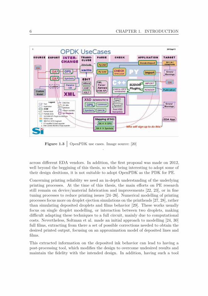
Starting on 2009, the Si2 foundation first presented OpenPDK coalition [21], al-though it did not start presenting specifications until mid-2010. This alliance ofEDA vendors proposed an unique design kit specification (OPDK), based on aneXtensible Markup Language (XML) database. Fig. 1.3 shows the general usecases for this PDK. The whole specification defines the basic representation ofthe necessary information necessary for circuit design (the interchange area on thefigure), and the mechanisms used to use this information in the EDA tools (thetransclude, parse, and check areas on the figure). Although this is not specificto PE, it could be adapted and extended for it. On the other hand, the maindisadvantage is that is still under development (changes could affect the extensionsfor PE technologies), is not fully public, and still there is not a wide adoption
6 CHAPTER 1. INTRODUCTION
Figure 1.3 OpenPDK use cases. Image source: [20].
across different EDA vendors. In addition, the first proposal was made on 2012,well beyond the beggining of this thesis, so while being interesting to adopt some oftheir design desitions, it is not suitable to adopt OpenPDK as the PDK for PE.
Concerning printing reliablity we need an in-depth understanding of the underlyingprinting processes. At the time of this thesis, the main efforts on PE researchstill remain on device/material fabrication and improvements [22, 23], or in finetuning processes to reduce printing issues [24–26]. Numerical modelling of printingprocesses focus more on droplet ejection simulations on the printheads [27, 28], ratherthan simulating deposited droplets and films behavior [29]. These works usuallyfocus on single droplet modelling, or interaction between two droplets, makingdifficult adapting these techniques to a full circuit, mainly due to computationalcosts. Nevertheless, Soltman et al. made an initial approach to modelling [24, 30]full films, extracting from there a set of possible corrections needed to obtain thedesired printed output, focusing on an approximation model of deposited lines andfilms.
This extracted information on the deposited ink behavior can lead to having apost-processing tool, which modifies the design to overcome undesired results andmaintain the fidelity with the intended design. In addition, having such a tool
1.3. THESIS CONTEXT 7
will finally bridge the step going from design to manufacturing. The design of thecharacterization procedure needed to extract this knowledge and the implementationof this tool are covered on chapters 4, and 5 respectively.
1.3 Thesis context
This work is framed inside two research projects: The Technology and Design Kits forPrinted Electronics (TDK4PE) project, European project [31], and the ApplicationSpecific Printed Electronic Circuits - Technology Design Kits (ASPEC-TDK) project,funded by Spanish government [32].
One of the main objectives of these projects is to provide a methodology whichenables PE circuit implementation, based on (and extending) current silicon micro-electronics methodologies. This will achieve a reduction of costs and time to marketof circuits based on PE technologies.
Inside these projects, the work of this thesis can be divided in two differentiatedparts, one focused on developing and adapting design flows and EDA tools towork with PE, and another focused on providing a characterization methodologyfor modelling the printing processes while extracting key printing information todevelop compensation operations, and the associated tools used to convert designsto something directly manufacturable.
To cover the first part, this work proposes a common database containing all PEinformation needed to customize existing EDA tools. Then, each different EDA toolswill access this database by means of an Application Programming Interface (API),or a set of specific converters. The design of this database has been performed underthe TDK4PE project, in collaboration with one of the project partners: PhoeniXsoftware [33].
In order to cover the last part, we need extensive knowledge of the underlyingprinting procedure, specially the ink behaviour when deposited. Modelling thiswe can compensate and correct some effects, like ink spreading, line bulging, orshape changes due to coalescense, to increase the printing fidelity and obtain finalmorphologies resembling as much as possible to the designed ones.
While previous works propose an initial approach to numerically model printedlines [24, 30], and other works focus on substrate-droplet or droplet-droplet sim-ulations [27, 28], this approach is not scalable to full circuits, mainly due to thecomputational complexity of these techniques. This work proposes a differentapproach to extract compensation information than the one proposed by Soltman etal. [30]. Building up from the results of different expected printing effects [34, 35],
8 CHAPTER 1. INTRODUCTION
instead of numerically model the film deposition, we create a semi-automated char-acterization setup based on both optical and electrical characterization. This allowsthe mass-characterization of printed samples, so by fabricating a large amount oftest samples with different corrections, and by applying different image processingalgorithms and statistical procedures, we can evaluate which correction producesa better improvement with statistical confidence, thus minimizing the effects pro-duced by printing issues not caused by the correction itself (e.g. nozzles clogged ornon-matching ejection velocities).
1.4 Aims and objectives
This thesis aims to provide a general design flow and kit, specifically tailored for PE.All the needed information for such kit will be backed up by a database, making itaccessible to several different EDA tools. In addition, a custom EDA componentwill be developed to cover the final conversion step to obtain manufacturabledesigns. This component will perform all necessary Fluidic Effects Correction (FEC)techniques to increase the design fidelity to the fabricated circuits.
To be able to cover these aims, the objectives of this thesis are twofold. The firstmain objective comprises the design of a suitable design flow for PE, based oncurrent microelectronics design flows. This design flow will cover the steps for basicfull-custom circuit design (schematic and layout entry, electrical simulation, andverification tools, such as DRC and Layout Versus Schematic (LVS)). In addition,all relevant technology information needed will be stored in a database, easy toaccess from different EDA tools. Therefore the detailed steps necessary to achieveit are:
• Construct a suitable database to represent all information related to PEprocesses, being easily accessible to EDA:
– Develop the database representation. Use an extensible structured format,while being easily parseable.
– Define an API to manipulate the data from EDA tools, and create a setof standalone generators for extracting useful information from it. Thisstep allows the connection of distinct EDA tools.
• Customize a full-custom design environment oriented to PE circuit designs:
– Customize a schematic entry program, containing the available PE devicesalong their parameters.
1.4. AIMS AND OBJECTIVES 9
– Integrate specific PE device models into an electrical simulator (SPICE-like). Together with schematic capture will allow easy simulation of PEcircuits without requiring full layout and fabrication.
– Customize a physical layout tool. This tool will act as the core of thedesign process, allowing the drawing of the final design to manufacture.To ease the design steps, a set of Parameterizable Cells (PCells) will beprovided, reducing design time and containing layout pieces which arecorrect by construction.
– Create a set of verification procedures to ensure design validity. Thisincludes DRC checks for layout, and a netlist extraction script to performLVS checks.
The second main objective is the creation of a tape-out tool for PE. This toolwill convert designed layouts to files directly understandable by the printer. Thisconversion will incorporate the FEC rules which will correct the printing issues,and obtain a final fabricated result which reproduces the intended design with morefidelity. To achieve this objective we need to:
• Study and quantify how the ink behaves when deposited, in order to extractwhich corrections are needed. To accomplish this is necessary to:
– Build a semi-automated characterization setup to characterize printedstructures optically and electrically. A semi-automated setup will allowmass-characterizatinon of test structures, therefore increasing the statis-tical significance of the extracted results. This allows the reduction ofthe noise caused by spurious printing defects.
– Design a set of different test structures and possible compensation op-erations to extract necessary corrections. The tested structures will beshapes commonly appearing in circuit and devices layouts, thus ensuringthat compensation operations also apply to bigger circuits. The pro-posed compensations are built upon previous results describing expectedprinting defects.
– Define a metric which evaluates each different compensation operationsso they can be evaluated. This metric scoring the performance of eachdifferent compensation is essential for statistical analysis.
– Implement a set of image processing algorithms, able to analyze eachcaptured image, align and superpose against a test template containingthe expected results, and using the previous defined score metric eval-uate the performance of the compensation. In addition, this analysiswill perform basic image pre-conditioning like removing satellite drops,providing additional printing quality information.

10 CHAPTER 1. INTRODUCTION
• Using computational geometry algorithms, implement the extracted compen-staion operations on the tape-out EDA component. These algorithms willanalyze the design layout, detect areas of interest where compensations shouldbe applied, perform all needed transformations, and generate a set of filesunderstandable by the printing equipment.
Covering all these objectives we will achieve a complete design environment adaptedto inkjet PE technologies, and achieving the abstraction between the different steps.
This thesis is outlined as follows: Chapter 2 describes design flows and kits, andintroduces the characterization environment. On chapter 3 contains the descriptionof the information database, and how is used to customize two sets of EDA tools.Chapter 4 explains the characterization procedures to analyze the printed shapesand extract suitable compensations, along to the statistical analysis performed, andchapter 5 describes the tape-out tool implementation. Finally, chapter 6 draws thefinal conclusions and gathers the future work and open ressearch lines.
Design Flows, Tools andKits 2
This chapter covers a review of the design kit, design flow and EDA tools concepts,and their application in PE.
First we will see the different abstraction levels from traditional microelectronicstechnologies, and the status of PE. Then, we will review the different designflows available. Last, we will cover the characterization setup and how the result-ing technology information will feed the design kits for their further EDA toolscustomization within the design flow.
2.1 Abstraction levels and design flows
There has been an increase of the level of abstraction during the evolution ofthe EDA tools for traditional silicon-based microelectronics. This raise of theabstraction has followed the development of the technology, and the increment ofthe complexity of the designs [36, 37]. We can see this evolution on Fig. 2.1.
Following the technology maturity evolution, the first abstraction level kept onworking at transistor level design with electrical simulation. The designs werecaptured at layout or schematic level, and simulations performed with SPICE-likesimulators [38, 39] with basic device models and capacity loads for timing analysis.As technology and design complexity increases, the abstraction level has to increasetoo. Therefore, the abstraction contemplates the concept of cells, as a cluster oftransistors with a certain functionality, and introduces logical gate-level models andbehavioral simulators. As technology evolves, gates are clustered into cells, andcells into Intellectual Property (IP) blocks; and design entry is shifted to hardware
11
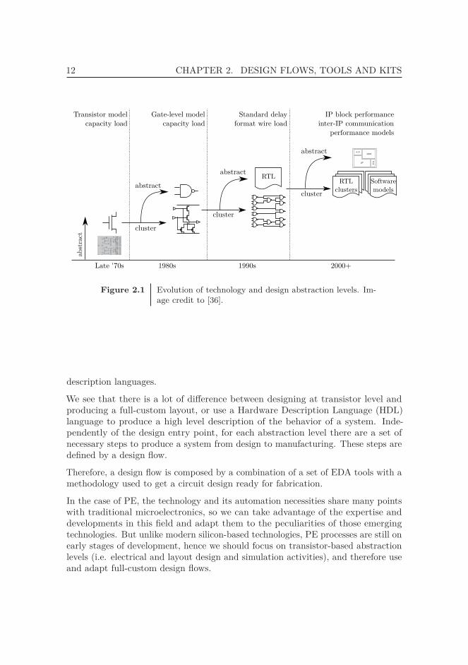
12 CHAPTER 2. DESIGN FLOWS, TOOLS AND KITS
Late '70s 1980s 1990s 2000+
RTL RTLclusters
Softwaremodels
cluster
abstractcluster
abstract
abstract
abst
ract
Transistor modelcapacity load
Gate-level modelcapacity load
Standard delayformat wire load
IP block performanceinter-IP communication
performance models
cluster
P
A/DRAM
Rnd
Figure 2.1 Evolution of technology and design abstraction levels. Im-age credit to [36].
description languages.
We see that there is a lot of difference between designing at transistor level andproducing a full-custom layout, or use a Hardware Description Language (HDL)language to produce a high level description of the behavior of a system. Inde-pendently of the design entry point, for each abstraction level there are a set ofnecessary steps to produce a system from design to manufacturing. These steps aredefined by a design flow.
Therefore, a design flow is composed by a combination of a set of EDA tools with amethodology used to get a circuit design ready for fabrication.
In the case of PE, the technology and its automation necessities share many pointswith traditional microelectronics, so we can take advantage of the expertise anddevelopments in this field and adapt them to the peculiarities of those emergingtechnologies. But unlike modern silicon-based technologies, PE processes are still onearly stages of development, hence we should focus on transistor-based abstractionlevels (i.e. electrical and layout design and simulation activities), and therefore useand adapt full-custom design flows.
2.2. PE DESIGN FLOWS 13
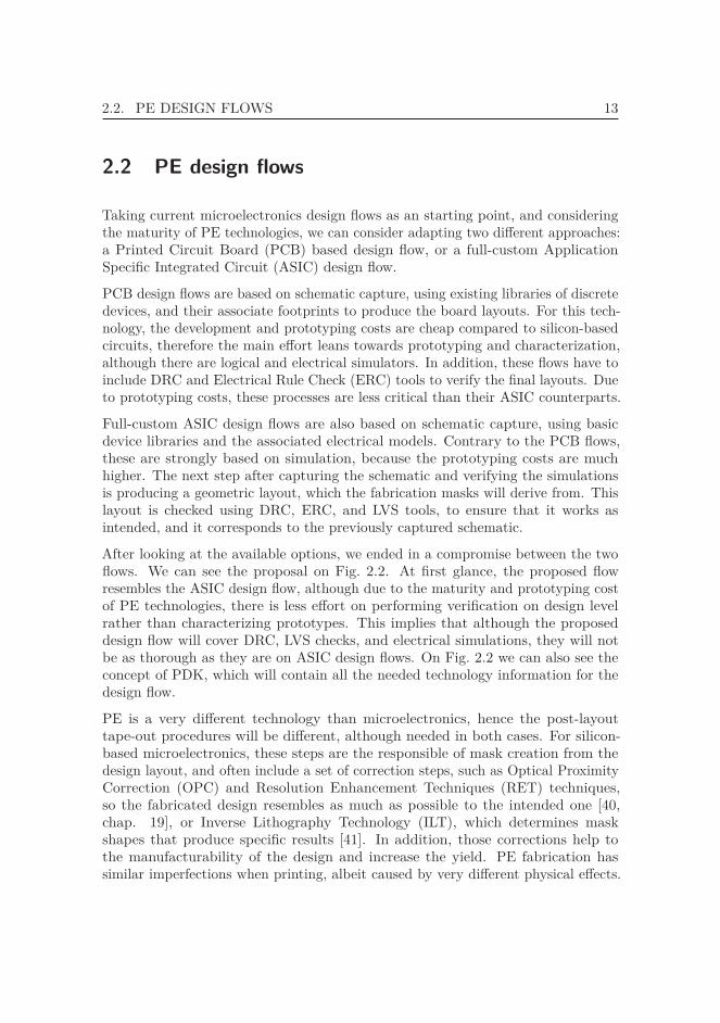
2.2 PE design flows
Taking current microelectronics design flows as an starting point, and consideringthe maturity of PE technologies, we can consider adapting two different approaches:a Printed Circuit Board (PCB) based design flow, or a full-custom ApplicationSpecific Integrated Circuit (ASIC) design flow.
PCB design flows are based on schematic capture, using existing libraries of discretedevices, and their associate footprints to produce the board layouts. For this tech-nology, the development and prototyping costs are cheap compared to silicon-basedcircuits, therefore the main effort leans towards prototyping and characterization,although there are logical and electrical simulators. In addition, these flows have toinclude DRC and Electrical Rule Check (ERC) tools to verify the final layouts. Dueto prototyping costs, these processes are less critical than their ASIC counterparts.
Full-custom ASIC design flows are also based on schematic capture, using basicdevice libraries and the associated electrical models. Contrary to the PCB flows,these are strongly based on simulation, because the prototyping costs are muchhigher. The next step after capturing the schematic and verifying the simulationsis producing a geometric layout, which the fabrication masks will derive from. Thislayout is checked using DRC, ERC, and LVS tools, to ensure that it works asintended, and it corresponds to the previously captured schematic.
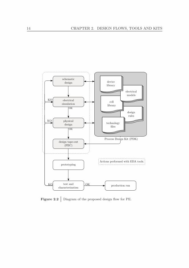
After looking at the available options, we ended in a compromise between the twoflows. We can see the proposal on Fig. 2.2. At first glance, the proposed flowresembles the ASIC design flow, although due to the maturity and prototyping costof PE technologies, there is less effort on performing verification on design levelrather than characterizing prototypes. This implies that although the proposeddesign flow will cover DRC, LVS checks, and electrical simulations, they will notbe as thorough as they are on ASIC design flows. On Fig. 2.2 we can also see theconcept of PDK, which will contain all the needed technology information for thedesign flow.
PE is a very different technology than microelectronics, hence the post-layouttape-out procedures will be different, although needed in both cases. For silicon-based microelectronics, these steps are the responsible of mask creation from thedesign layout, and often include a set of correction steps, such as Optical ProximityCorrection (OPC) and Resolution Enhancement Techniques (RET) techniques,so the fabricated design resembles as much as possible to the intended one [40,chap. 19], or Inverse Lithography Technology (ILT), which determines maskshapes that produce specific results [41]. In addition, those corrections help tothe manufacturability of the design and increase the yield. PE fabrication hassimilar imperfections when printing, albeit caused by very different physical effects.
14 CHAPTER 2. DESIGN FLOWS, TOOLS AND KITS
schematicdesign
electricalsimulation
physicaldesign
prototyping
test andcharacterization
design tape-out(FEC)
OK
OK
designrules
celllibrary
electricalmodels
technologyles
devicelibrary
Process Design Kit (PDK)
KO
KO production run
KO
OK
Actions performed with EDA tools.
Figure 2.2 Diagram of the proposed design flow for PE.
2.3. PROCESS DESIGN KITS 15
EDA ToolsDesign Flow
Info forProcess DesignKits (PDKs)
Blocks & celllibraries
Basicdevices
Technologyprocesses
DevelopmentCharacterization
& Modelling
Figure 2.3 PDK development and characterization, and EDA cus-tomization loop.
Therefore we need a last step on the flow which will convert the design to a set ofprintable files. This conversion step includes the necessary FEC corrections, whichact as the RET counterparts for PE. The FEC techniques and the tool performingthe tape-out procedure are covered in detail on chapters 4, and 5.
2.3 Process Design Kits
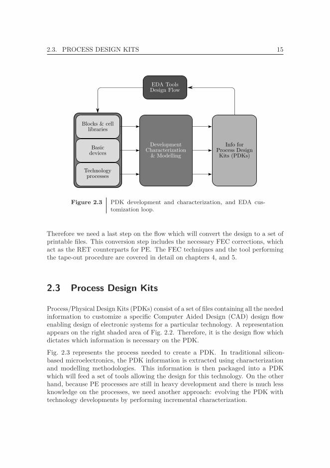
Process/Physical Design Kits (PDKs) consist of a set of files containing all the neededinformation to customize a specific Computer Aided Design (CAD) design flowenabling design of electronic systems for a particular technology. A representationappears on the right shaded area of Fig. 2.2. Therefore, it is the design flow whichdictates which information is necessary on the PDK.
Fig. 2.3 represents the process needed to create a PDK. In traditional silicon-based microelectronics, the PDK information is extracted using characterizationand modelling methodologies. This information is then packaged into a PDKwhich will feed a set of tools allowing the design for this technology. On the otherhand, because PE processes are still in heavy development and there is much lessknowledge on the processes, we need another approach: evolving the PDK withtechnology developments by performing incremental characterization.
16 CHAPTER 2. DESIGN FLOWS, TOOLS AND KITS
This evolutive approach allows having a very basic PDK early, therefore being ableto customize a set of EDA tools. Taking advantage of the automation facilities ofthese tools, we can use them to assist on test vehicle and generating large amountof test structures, improving the technology characterization and PDK refinement.Hence we will start by basic characterization of print processes and go up to basicdevices and cells modelling, generating an updated PDK at each iteration. Tobe able to cope with the characterization of large amount of samples we need asemi-automatic characterization setup, described on section 2.4.
2.3.1 Necessary process information
Depending on the design flow step, the tool covering it will need some technologyrelated information. This section will outline which information is needed on thedifferent steps of the design flow.
Schematic design and Electrical simulation
Because it is a netlist description specifying the connections of basic devices,schematic entry itself is not a technology dependent step. Therefore, schematiccapture programs need a basic library of all the available devices on a particulartechnology. Each device is comprised of the device symbol with the related cus-tomizable design parameters (p.e. W/L values for transistors), and a reference toits model.
In order to perform electrical simulation, the design kit needs access to the electricalmodels for the available devices. Therefore, for each device in the library, the designkit has to include its electrical model.
Physical design
To be able to represent physical layouts, the EDA tools need to know which layersare available in the technology. In addition to their graphical properties, the layouteditor needs to be aware of connectivity information, so it can extract devices andnets to build a netlist file, as well as the extracted DRC rules used for verificationpurposes.
2.3. PROCESS DESIGN KITS 17
Design tape-out and FEC tools
These tools are the most dependent on technology processes of the design flow. Inorder to perform the design conversion and correction, they need to know specificparameters for each process step, either the physical parameters or some appropriateempirical abstractions.
2.3.2 XML interface
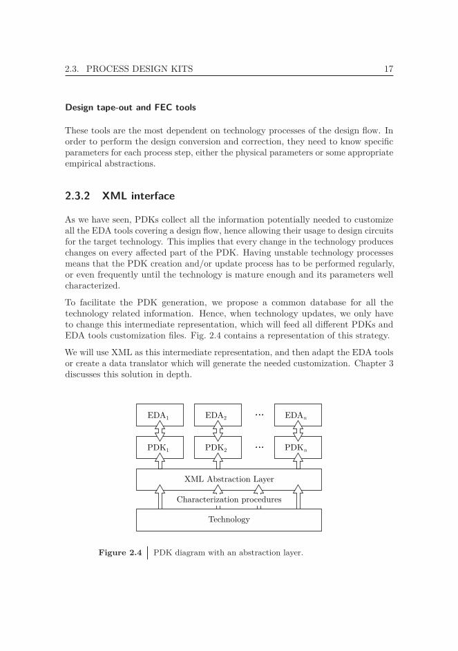
As we have seen, PDKs collect all the information potentially needed to customizeall the EDA tools covering a design flow, hence allowing their usage to design circuitsfor the target technology. This implies that every change in the technology produceschanges on every affected part of the PDK. Having unstable technology processesmeans that the PDK creation and/or update process has to be performed regularly,or even frequently until the technology is mature enough and its parameters wellcharacterized.
To facilitate the PDK generation, we propose a common database for all thetechnology related information. Hence, when technology updates, we only haveto change this intermediate representation, which will feed all different PDKs andEDA tools customization files. Fig. 2.4 contains a representation of this strategy.
We will use XML as this intermediate representation, and then adapt the EDA toolsor create a data translator which will generate the needed customization. Chapter 3discusses this solution in depth.
XML Abstraction Layer
EDA1 EDA2 EDAn
PDK1 PDK2 PDKn
Characterization procedures
Technology
Figure 2.4 PDK diagram with an abstraction layer.
18 CHAPTER 2. DESIGN FLOWS, TOOLS AND KITS
.jpgs-video
digitalizer
host computer with LabVIEW application
GPIB/ethernets-video
USB
measurementsdatabase
acquisitioninstrument 1
acquisitioninstrument 2
acquisitioninstrument N
Cascade MicrotechProbestation
test vehiclesdescription le
TVD
.csv
Figure 2.5 Characterization environment setup. The diagram contem-plates both optical and electrical characterization.
2.4 Characterization strategies and setup
As commented, in order to extract a PDK for a PE technology following theprocedure outlined on Fig. 2.3, we need to automate the characterization step toavoid it being the bottleneck of technology evolution. This progressive refinementand the maturity of the technology means that a large amount of samples will becharacterized, therefore needing a semi-automatic procedure able to cope with thesamples volume.
The characterization setup is built around a host computer controlling CascadeMicrotech Summit Series 12000 probe station in combination with all the requiredmeasurement instruments, and is shown on Fig. 2.5.
This probe station has been adapted to work with flexible plastic substrates, and is
2.5. CONCLUSIONS 19
equipped with a Leica S6D microscope and a video capture device. Using a set ofLabVIEW 2013 programs we can control all the setup equipment, thus being ableto configure, control the actions, query the status, and exchange data. This allowssmart characterization protocols which performs different actions depending on themeasured data and capture still images of the devices under test.
The whole characterization procedure starts with the Test Vehicle Description (TVD)file, which is automatically generated using the EDA tools scripting facilities. Thisfile contains all the relative position of the samples under test, and each sampleparameters and identification for tracking and posterior analysis purposes. Withthis information, the LabVIEW procedures on the host computer drive the probestation movements and all connected equipments, performing the correspondingmeasurements, and capturing an image.
After the characterization of the foil finishes, the host computer generates andexports a Comma-Separated Values (CSV) file with the results, and saves it withthe captured images.
2.5 Conclusions
In a general sense, PE processes share a lot of characteristics with their microelec-tronics counterparts. Therefore, it makes sense to adapt existing microelectronicsdesign flows to PE technologies, hence taking advantage of the expertise of thisarea. But there are particular needs that those already established flows do notcover, hence requiring some specific in-depth adaptations.
Because of the still low maturity of the technology, all the processes are constantlyevolving, so all the information included inside the PDK is prone to change. To beable to cope with this evolution, we need some representation that will help changingit without much effort, hopefully decreasing the necessary work, thus reducingpossible error. We developed an specific XML database representation specificallytailored to printing PE technologies to collect and exploit PDK information.
This XML intermediate representation, in addition to concentrating all the infor-mation in a common place, facilitates PDK generation for several different EDAtools, therefore obtaining a twofold advantage. First, once a tool supports thisrepresentation, any technology change will be reflected automatically on the PDK,and secondly, by having a complete representation it is possible to describe a com-pletely new technology and generate all the PDKs automatically, without makingany change to the supported EDA tools. In addition, each time the parameterschange, just updating the XML information and all the PDKs will be automaticallyup to date.

20 CHAPTER 2. DESIGN FLOWS, TOOLS AND KITS
The semiautomatic characterization system developed at ICAS group provides anautomated probe station and equipment controlling, having tracking information(i.e. position and parameters) for each tested sample, and automatic data dataextraction and analysis. The whole setup is driven by a set of LabVIEW controlsubroutines which read the generated TVD file, therefore providing an automatedpath from test vehicle generation to characterization, thus making a less error pronesystem reducing human interaction, and speeding up technology characterization.
The proposed intermediate representation and its usage is discussed thoroughly onchapter 3, together with two use cases for two different set of tools and differenttechnologies. Chapter 5 describes the framework used to perform the FEC andconversion for design post-processing.
Specific Design Kits andEDA tools for PE 3
This chapter covers the specific details of the generated PDKs for PE. First ofall, the chapter contains a revision of the EDA tools used to cover the design flow,leading to the discussion of the design kit intermediate representation and its usage.
As a concluding section, we will show two different technologies adapted to this setof tools: an inkjet process, and a gravure process.
3.1 EDA tools selection
On this section we will discuss which set of tools will be used to cover the proposeddesign flow. First we will discuss a set of free (and if possible open source) tool set,and then a commercial tool package.
The main characteristics we search for are that the tool is easy to install, customize,and maintain, while being cross-platform software. In addition, the layout editor, andassociated tools, should support arbitrary geometries and contain basic verificationtools such as DRC, netlist extraction, and LVS.
All the tools should be able to import and export to different file formats, followingthe industry standards, and if possible, contain scripting facilities to ease thecustomization steps, allow procedural layout development using PCells, and simplifytool linking and sistematic steps.
A part from the set of EDA tools evaluated, the design flow will be mapped ontop an available commercial EDA package already fixed in the framework of theTDK4PE European project.
21
22 CHAPTER 3. SPECIFIC DESIGN KITS AND EDA TOOLS FOR PE
3.1.1 FOSS tool set
This section contains the discussion of the Free/Open Source Software (FOSS) toolset. In order to cover the flow, we need a layout editor, a schematics editor and anelectrical simulator.
Along this chapter, the usage of FOSS will not be precise because it also will includesome tools which are free (as in gratis) but not open source.
Layout editor
The first tested layout editor has been Toped [42]. Toped is a multi-platform layouteditor, supporting GDS, OASIS, and CIF. It is an open source software whichis still under development. As major advantages, the editor is free and supportsstandard input/output file formats. In addition, it can import Cadence® technologyfiles. On the other hand, the editor does not come with its own verification tools,although it can import Calibre errors, and the PCell support is limited.
Glade IC [43] is a free (not open source) layout editor able to read and write awide range of file formats. The program is scriptable using Python and is underactive development. In addition, it has basic DRC, extractor, and LVS tools (thislast one using Gemini [44]), and supports the usage of PCells. A part from its owntechnology file format it can import several other EDA formats such as Cadence®
technology files.
Electric VLSI [45] is a schematic and layout editor, free and open source, andmulti-platform. It is under active development and also supports a wide range ofinput/output file formats. It contains verification tools, such as DRC, and ERC.The design entry is very different from traditional EDA tools, because is stronglybased on connectivity. This makes LVS checks immediate, as both schematic andlayouts are captured placing nodes (the components themselves) and arcs (theconnectors or wires), therefore have connectivity information. As a drawback, thisencumbers designers when they want to draw arbitrary geometry shapes, and canlead to inconsistent results, as touching shapes are not necessary actually connected.
Magic VLSI [46] is a venerable layout editor quite popular in universities and smallcompanies. It is free and open source, and under active development. It is capableof importing and exporting to standard file formats and has several verificationtools for LVS and DRC. On the other hand, it is a complex and unintuitive software(operated using commands), and it only supports “Manhattan geometries”. Inaddition, Magic is not a cross-platform program (without using an emulator).
Table 3.1 contains a summary of the reviewed characteristics for each layout editor

3.1. EDA TOOLS SELECTION 23
Toped Glade Electric Magic
Support reading multiple input outputdesign formats (at least GDS). � � � �
Support Cadence® technology files. � � � �
Arbitrary geometry and drawing sup-port. � � �1 �
Easily scriptable (for customization). �2 � � �
Creation of PCells. �2 � � �
DRC verification. �3 � � �3
LVS verification. � � � �4
Netlist extraction. � � � �4
Cross platform support. � � � �
Ease of use (and similarity to other VLSIlayout editors). � � � �
Opensource software � � � �
1While allowing drawing arbitrary shapes, it is based on connectivity, not on arbitraryshapes drawing.2Using a not widely used, proprietary language.3Can import DRC results from Calibre.4Only for manhattan geometries.
Table 3.1 Summary of the main characteristics for each layout editorevaluated.

24 CHAPTER 3. SPECIFIC DESIGN KITS AND EDA TOOLS FOR PE
XCircuit KiCad gschem
Scriptable for inter-tool communication. � � �
Standalone program (not part of othernon-suitable EDA suite. � � �
Custom symbol with custom attributes. � � �
SPICE simulator connection/netlist ex-traction. � � �
Cross platform support. � � �
Table 3.2 Summary of the main characteristics for each schematiccapture program evaluated.
program. After the review, the most suitable tool seems to be Glade IC. Althoughit is not open source, its API provides access to all the inner parts, thus makinga very extensible program. It is also extended using Python, which is a popularlanguage, aiding with the customization and integration with other tools.
Schematic editor
XCircuit is the schematics capture part by the same author as Magic VLSI [47].Although it has a small library of standard symbols and can connect with electricalsimulators, it is thought more as a general purpose drawing program. The usageis similar as Magic, therefore it is not very intuitive nor simple to use. The mainissue is the same as Magic, this software is not cross-platform.
KiCad [48] is an EDA suite for schematics capture and PCB board design. It is anextensible, cross-platform solution, although is highly oriented to a PCB flow.
gEDA project [49], as does KiCad, provides a set of open source, cross-platform EDAtools. They also provide a full PCB flow, with schematics capture and simulation,but unlike KiCad, all the different tools are loosely coupled, thus facilitating usingonly part of the suite. All the different tools are built around a scheme API,therefore the whole set of EDA components are fully customizable.
Table 3.2 contains the summary of the evaluated characteristics for the shcematiccapture program. We choose gschem and gnetlist components of the gEDA suitebecause they are less coupled than its KiCad counterparts, maintaining similarcapabilities. All the gEDA suite is built around the gEDA library which is totally

3.1. EDA TOOLS SELECTION 25
ngspice gnucap
SPICE like simulator. � �
Support of custom models usingVerilog-A. � �1
Industrial strength simulator. � �
1Although custom models are supported, at the time of theevaluation the only option was to use the model compiler andnot Verilog-A.
Table 3.3 Summary of the main characteristics for each electricalsimulator program evaluated.
accessible by the scripting API. This facilitates the extension, adding extra func-tionalities, and connecting the tool with the other ones which compose the designflow.
Electrical Simulator
PE produced devices usually are not modelled using traditional device modelscoming from microelectronic technologies. Hence, the electrical simulator has tosupport some way of custom model inclusion. The industry standard for codingdevice models is to use Verilog-A [50], along with the proposed extensions for devicemodelling [51].
Ngspice [52, 53] is an open source port of the traditional Berkeley SPICE3f5 engine.In addition to implementing all SPICE functionality, it also integrates XSPICEextensions from Georgia Tech [54] for mixed signal simulation, and basic Verilog-Amodel loading through ADMS [55], which parses a subset of Verilog-A standardand transforms to C code following SPICE simulator interfaces.
Gnucap [56, 57], is the GNU Circuit Analysis package, consisting in a generalpurpose circuit simulator. It is not based on SPICE, although some models havebeen ported from their SPICE implementations. The engine is designed to be trulymixed mode, supporting event driven simulations. At the time of this evaluation,custom models had to be implemented using its model compiler [58], and it did notsupport loading Verilog-A compact models.
Therefore, we chose the ngspice simulator, because it is a industrial strengthimplementation of the SPICE simulator, with several standard models compiled in,and the ability to integrate custom models using Verilog-A with ADMS.
26 CHAPTER 3. SPECIFIC DESIGN KITS AND EDA TOOLS FOR PE
3.1.2 Commercial tools
The commercial package covering the design flow is MaskEngineer together withCleWin, from PhoeniXTM software. MaskEngineer is a professional, object oriented,and parametric layout package. This tool expects that all layouts are describedparametrically using the provided scripting language (PhoeniX script). Describingit in a mathematical way increases design reuse, and just by changing parameters,MaskEngineer generates the layout. CleWin is a hierarchical layout editor containingbasic drawing primitives and a scripting engine.
MaskEngineeer engine contains a boolean package supporting geometric manipula-tion operations, and a built-in DRC tool.
This tool set covers the layout and verification steps. To cover the schematic capture,CleWin has been extended to be more integrated to the common PDAFlow API [59].This integration allows direct access to the design kit components, and is capable ofplacing an icon view of the component. Effectively this provides schematic capturecapabilities to this layout editor, with the advantage of being able to generate thelayout directly from the same software.
As for electrical simulator, the commercial EDA package is capable of exporting toSPICE format, therefore ngspice is also used.
3.2 EDA tool customizations
After the discussion, we can see the whole design flow and the tools that cover iton Fig. 3.1. The figure contains the proposed set of FOSS tools covering the flow,and an existing commercial package. This integration will demonstrate further theextensibility of the proposed design kit structure.
3.2.1 Free/Open source tool selection
After the evaluation of the FOSS tools, and concerning all options available on 2010(the time when the evaluation and analysis was performed) we choose to cover thewhole flow with:
• Glade IC (and integrated tools) for layout, DRC, LVS, and extraction.
• gschem and gnetlist from gEDA for schematics capture and netlist extraction.
• ngspice for electrical simulation.
3.2. EDA TOOL CUSTOMIZATIONS 27
inks, substrate andprocesses
characterization
printerspeci cations
technologyle compensation
rules
layoutle
(GDS)
nalle
(BMP)
DRCle
compensationtool
DRCtool
layouteditor
schematicor netlist
LVS &ERC
extractiontool
extractednetlist
electricalsimulation
ngspice
schematiceditor
L2B
spice XML
GDS
spice
XMLXML
BMP
XML
OSS owFile format
Commercial ow
gschemgnetlistCleWin
gladeMaskEngineer
gladeMaskEngineer
gladeMaskEngineer
gladeMaskEngineer
Figure 3.1 Complete design flow, containing all used tools and inter-mediate formats. The diagram contains both the FOSSand the commercial flow. This diagram can be seen as adetailed version of Fig. 2.2

28 CHAPTER 3. SPECIFIC DESIGN KITS AND EDA TOOLS FOR PE
This set of tools covers all steps needed to produce a design from schematic captureto layout, but there are still some missing features that need an in-depth attention.
The first one is the model inclusion inside the electrical simulator. PE transistorsare usually modelled using UMEM [60, 61] into the Unified Compact Model. Thismodel is not integrated into the simulators. In order to include the model insidethe simulator we performed the following steps:
• Modify ADMS source code support inside the ngspice simulator to supportadditional Verilog-A functionalities: support for analog functions constructs.
• According to ngspice manual [53, chap. 13], modify device parsing and loadingcode to support the custom Verilog-A model.
• Modification of transistor evaluation code to support 3-terminal devices(transistors without bulk).
• During the evolution of this work, more devices other than transistors havebeen modelled using Verilog-A. Therefore, we extended the simulator resistorand capacitor devices model loading code to support Verilog-A models.
In addition to this work, the contact with ngspice developers for support, and laterfor code patches and modifications led to contributions on the simulator main sourcecode tree.
The schematic editor and netlister needed some adaptations to include the devicesymbols and their model references, and customizations to automatically launchsimulations, read simulation parameters from designs, automatically include devicemodels, and support of hierarchical designs and dependency tracking between parts.Hence, the performed modifications to the gEDA suite are:
• A complete new set of symbols for the available devices.
• Scripting procedures to adapt gschem to the proposed design flow:
– Fixed and updated an auto-numbering script to facilitate schematiccapture. Until then all devices were not automatically numbered, leadingto errors on netlisting procedures.
– Custom procedures to automatically create a symbol for the currentschematic.

3.2. EDA TOOL CUSTOMIZATIONS 29
• A new netlisting backend1 which supports hierarchy (multiple schematics,and automatic detection of input/output ports), inclusion of electrical models,and simulation directives.
• An integrated project structure with a central Makefile controlling schematicactions:
– Automatic dependency tracking between a hierarchical design (regenerateaffected netlists when a schematic changes).
– Automatically launch simulations for the top design.– Automatically create a suitable netlist for LVS comparison.
For the layout editor, a part from all the PCell creation and verification scripts,we made some customizations to support the design flow and project structure.It automatically loads the design kit libraries, loads the current design (if any),and has custom menu entries to automatically export the design and convert it toprintable files. Therefore, the modification done to Glade IC are:
• Custom connectivity extraction script supporting 3-terminal transistors.
• Integration with project directory: At startup automatically detect whichdesign kit is loaded and if there is an existing project.
• Custom menu actions to integrate with the design flow:
– Flatten current design and load it to Layout2Bitmap– Initial design post-processing before tape-out: Generate derived layers
for manufacturing.
• Although the source code to Glade IC is not available, the LVS source is. Weadapted the program to compare 3-terminal devices.
The last step of the proposed flow on Fig. 3.1 is the equivalent of design tape-outfor PE, the creation of the bitmap files which will be sent to the printer. Thereare not any existing tool which will perform this procedures because they aretechnology specific. For this purpose, we developed a custom EDA framework(Layout2Bitmap) responsible to convert the designs to the appropriate formats, andapply the necessary corrections, transformations, and compensations. This tool isdetailed in chapter 5.
1The netlister program treats backends as programs which transform an input schematic to acertain netlist program. This provides a highly flexible approach, being able to generate differentnetlist formats, and hence supporting several simulators.
30 CHAPTER 3. SPECIFIC DESIGN KITS AND EDA TOOLS FOR PE
3.2.2 Commercial package
All the commercial tools are built around the PDAFlow API [59], so by adaptingthe XML intermediate representation of the design kit to this API we will achieveintegration into both MaskEngineer and CleWin.
MaskEngineer software was intended mainly to photonics applications and it didnot have a direct connection with an electrical simulator. Also, it was not possibleto seamlessly connect the MaskEngineer software with the custom EDA frameworkused to perform the tape-out procedure. To solve these topics, and during a researchstage in PhoeniX Software, we extended both MaskEngineer and Layout2Bitmapto manage this seamless integration:
• Layout2Bitmap plugin code to read design from PDAFlow API designs.
• Connecting code between PDAFlow API and the XML database describedon section 3.3 below.
• New MaskEngineer functions to export designs:
– Export as SPICE netlist and launch simulator.– Export design to Layout2Bitmap.
• Initial implementation and support for extra DRC checks.
3.3 XML database
Now we will address the XML database developed in order to collect all thetechnology information needed for its usage as a PDK for specific tools. We choosethis specific format because it gives a structured and human readable representationof information, while being easy to parse by a computer. In addition, it permits easyquerying and subsetting, therefore facilitating information retrieval or generation.During the XML description, we will outline which information is needed on eachstep of the design flow, and how it is handled by the database. This will lead to asuitable abstraction which achieves tool independence.
3.3.1 XML representation
The specific structure of the XML database will be divided into several differentparts describing the details of: layer definitions, design rules, compensation rules,
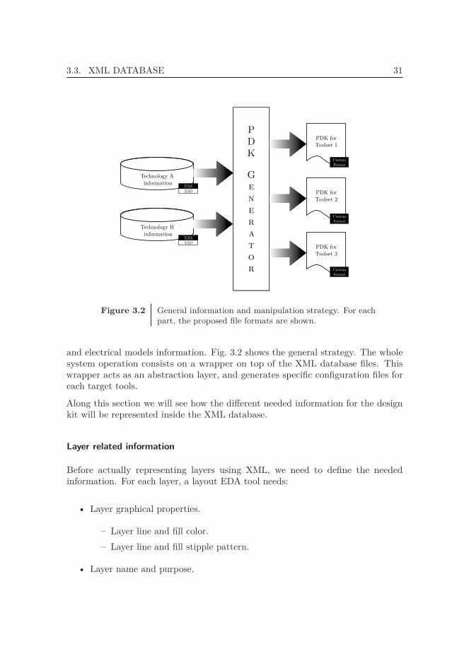
3.3. XML DATABASE 31
Technology A information
Technology B information
PDK forToolset 1
PDK Generator
PDK forToolset 2
PDK forToolset 3
XMLXSD
CustomFormat
CustomFormat
CustomFormat
XMLXSD
Figure 3.2 General information and manipulation strategy. For eachpart, the proposed file formats are shown.
and electrical models information. Fig. 3.2 shows the general strategy. The wholesystem operation consists on a wrapper on top of the XML database files. Thiswrapper acts as an abstraction layer, and generates specific configuration files foreach target tools.
Along this section we will see how the different needed information for the designkit will be represented inside the XML database.
Layer related information
Before actually representing layers using XML, we need to define the neededinformation. For each layer, a layout EDA tool needs:
• Layer graphical properties.
– Layer line and fill color.– Layer line and fill stipple pattern.
• Layer name and purpose.

32 CHAPTER 3. SPECIFIC DESIGN KITS AND EDA TOOLS FOR PE
• GDS layer number and datatype, for design import/export.
• Layer electrical properties (layer conductivity and capacity).
All of these properties cover all the information needed to support basic layoutdesign using a layout EDA tool.
The extract of XML Schema Definition (XSD) schema for a layer appears inlisting 3.1:
...<xs:complexType name="dlayer">
<xs:sequence><xs:element name="parameters" type="parameters"/>
...</xs:sequence><xs:attribute name="name" use="required" type="xs:NCName"/>
</xs:complexType>...<xs:complexType name="parameters">
<xs:sequence><xs:element name="short_name" type="xs:NCName" /><xs:element name="purpose" type="xs:NCName" /><xs:element name="gds_num" type="xs:short"/><xs:element name="gds_dtyp" type="xs:short"/><xs:element name="print_direction" type="xs:string"/><xs:element name="color" type="color"/><xs:element name="sel" type="xs:boolean"/><xs:element name="vis" type="xs:boolean"/>
...</xs:sequence>
</xs:complexType>...
Listing 3.1 Excerpt of the layer XSD definition.
And an example layer defined following that schema is shown on listing 3.2:
...<dlayers>
<dlayer name="OrgSC1"><parameters>
<short_name>OSC1</short_name><purpose>drawing</purpose><gds_num>60</gds_num><gds_dtyp>50</gds_dtyp><print_direction>Top-Down</print_direction><grid>20</grid>
3.3. XML DATABASE 33
<color name="" R="0" G="255" B="0" /><sel>true</sel><vis>true</vis><fillstyle>
<name>Slash1</name><bitmapFile>slash1.bmp</bitmapFile>
</fillstyle><linestyle>Solid</linestyle><function>-</function><printing_layer>1</printing_layer><design_layer>1</design_layer>
</parameters></dlayer>
...</dlayers>
Listing 3.2 Excerpt of the layer XML definition
Design Rules information
The case of the DRC rules is more complex than the layer characteristics. To have acomplete definition of all available checks, we need an extensible operation definition.XML format allows nested recursive statements, thus is possible to define a type asshown on listing 3.3:
...<xs:complexType name="dlayer_ref">
<xs:attribute name="gds_num" type="xs:short"/><xs:attribute name="gds_dtyp" type="xs:short"/>
</xs:complexType>...<xs:complexType name="operation">
<xs:choice minOccurs="1" maxOccurs="unbounded"><xs:element name="operation" type="operation"/><xs:element name="layer" type="dlayer_ref"/>
</xs:choice><xs:attribute name="name" use="required" type="xs:string"/><xs:attribute name="value" type="xs:double"/>
</xs:complexType>
Listing 3.3 Excerpt of the operation defintion schema.
Having this recursive definition, we can define complex geometrical layout oper-ations acting on single layers or any combination of them. Listing 3.4 shows theimplementation of eq. (3.1).
(Ly(60, 50) ∩ Ly(70, 40)) ∪ Ly(80, 30), (3.1)

34 CHAPTER 3. SPECIFIC DESIGN KITS AND EDA TOOLS FOR PE
where Ly(X, Y ) specifies a layer selection function selecting the layer with GraphicDatabase System (GDS) number X and datatype Y . By using this structure, wecan refer to a layer or any combination of layers of the design. A part from theDRC rules, the same definition is shared among the whole database sections whichneed querying layers.
<operation name="OR"><operation name="AND">
<layer gds_num="60" gds_dtyp="50" /><layer gds_num="70" gds_dtyp="40" />
</operation><layer gds_num="80" gds_dtyp="30" />
</operation>
Listing 3.4 Example of operation definition in the XML database.
After having this recursive definition of the operations, we can define the properDRC rules. Listing 3.5 contains an extract of the schema definition:
<xs:complexType name="interLayerRule"><xs:sequence>
<xs:element name="name" type="xs:NCName"/><xs:element name="layerA" type="layerSelector"/><xs:element name="drcOperation" type="drcOperation"/><xs:element name="layerB" type="layerSelector"/><xs:element name="value" type="xs:double"/><xs:element name="description" type="xs:string"/><xs:element name="error_msg" type="xs:string" />
</xs:sequence></xs:complexType>
Listing 3.5 DRC rule definition schema.
And an example rule is defined as shown on listing 3.6:
...<rule>
<name>GtC1.O</name><layerA>
<operation name="AND"><layer gds_num="100" gds_dtyp="10" /><layer gds_num="80" gds_dtyp="40" />
</operation></layerA><drcOperation>overlap</drcOperation><layerB><layer gds_num="100" gds_dtyp="10" /></layerB><value>25</value>
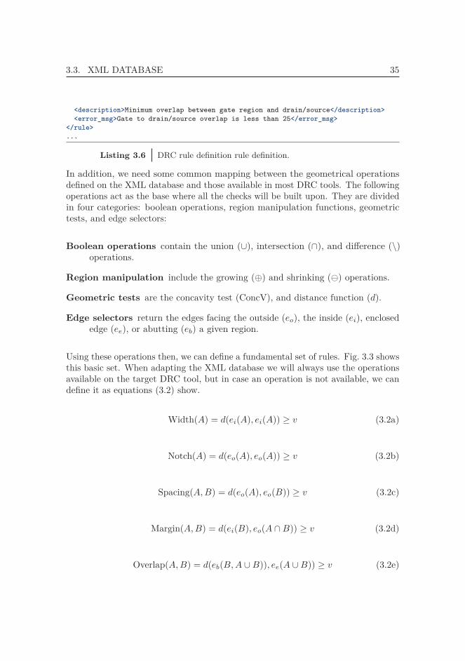
3.3. XML DATABASE 35
<description>Minimum overlap between gate region and drain/source</description><error_msg>Gate to drain/source overlap is less than 25</error_msg>
</rule>...
Listing 3.6 DRC rule definition rule definition.
In addition, we need some common mapping between the geometrical operationsdefined on the XML database and those available in most DRC tools. The followingoperations act as the base where all the checks will be built upon. They are dividedin four categories: boolean operations, region manipulation functions, geometrictests, and edge selectors:
Boolean operations contain the union (∪), intersection (∩), and difference (\)operations.
Region manipulation include the growing (⊕) and shrinking (�) operations.
Geometric tests are the concavity test (ConcV), and distance function (d).
Edge selectors return the edges facing the outside (eo), the inside (ei), enclosededge (ee), or abutting (eb) a given region.
Using these operations then, we can define a fundamental set of rules. Fig. 3.3 showsthis basic set. When adapting the XML database we will always use the operationsavailable on the target DRC tool, but in case an operation is not available, we candefine it as equations (3.2) show.
Width(A) = d(ei(A), ei(A)) ≥ v (3.2a)
Notch(A) = d(eo(A), eo(A)) ≥ v (3.2b)
Spacing(A, B) = d(eo(A), eo(B)) ≥ v (3.2c)
Margin(A, B) = d(ei(B), eo(A ∩ B)) ≥ v (3.2d)
Overlap(A, B) = d(eb(B, A ∪ B)), ee(A ∪ B)) ≥ v (3.2e)
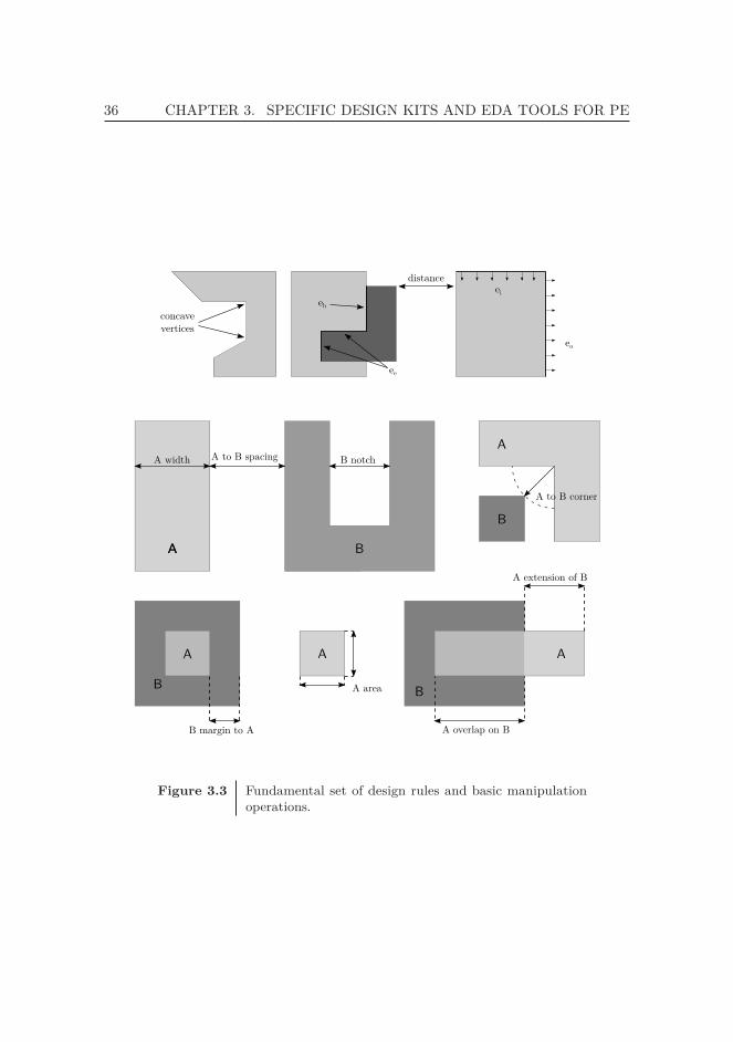
36 CHAPTER 3. SPECIFIC DESIGN KITS AND EDA TOOLS FOR PE
concavevertices
eb
ee
eo
ei
distance
A width
A
A to B spacing
B
B notch
A
A
B
A overlap on B
A
B
B margin to A
A
A area
A extension of B
A
BA to B corner
Figure 3.3 Fundamental set of design rules and basic manipulationoperations.
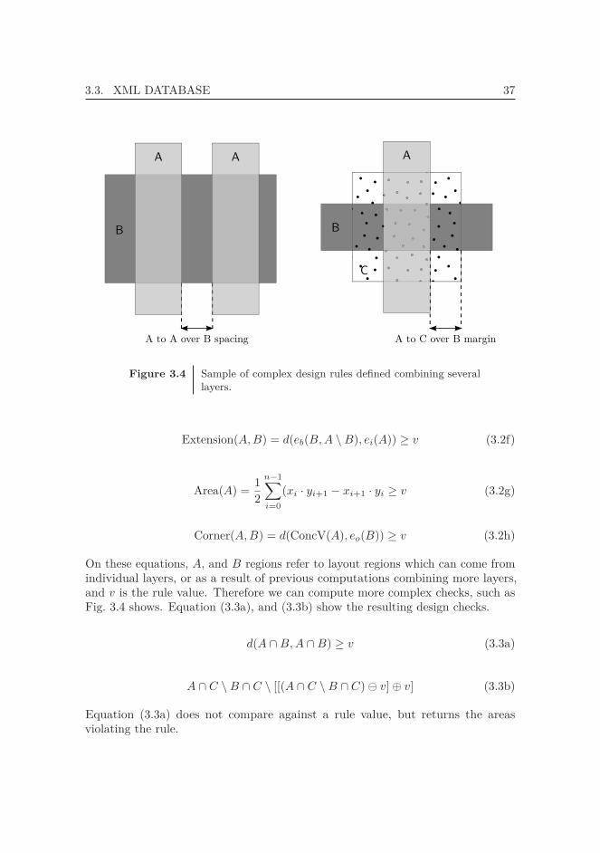
3.3. XML DATABASE 37
A to C over B margin
C
A
BB
A to A over B spacing
A A
Figure 3.4 Sample of complex design rules defined combining severallayers.
Extension(A, B) = d(eb(B, A \ B), ei(A)) ≥ v (3.2f)
Area(A) = 12
n−1∑i=0
(xi · yi+1 − xi+1 · yi ≥ v (3.2g)
Corner(A, B) = d(ConcV(A), eo(B)) ≥ v (3.2h)
On these equations, A, and B regions refer to layout regions which can come fromindividual layers, or as a result of previous computations combining more layers,and v is the rule value. Therefore we can compute more complex checks, such asFig. 3.4 shows. Equation (3.3a), and (3.3b) show the resulting design checks.
d(A ∩ B, A ∩ B) ≥ v (3.3a)
A ∩ C \ B ∩ C \ [[(A ∩ C \ B ∩ C) � v] ⊕ v] (3.3b)
Equation (3.3a) does not compare against a rule value, but returns the areasviolating the rule.

38 CHAPTER 3. SPECIFIC DESIGN KITS AND EDA TOOLS FOR PE
Electrical models information
Because representing the actual electrical model in XML is impractical due to itscomplexity, we include only the model metadata. This allows generating smallpieces of information needed by the simulators to use the actual model, and generatedocumentation about the model itself and usage instructions. Listing 3.7 shows theschema part dealing with model information:
<xs:simpleType name="modelLanguage"><xs:restriction base="xs:string">
<xs:enumeration value="verilogA"/><xs:enumeration value="spice"/><xs:enumeration value="vhdl-AMS"/>
</xs:restriction></xs:simpleType>
<xs:complexType name="model"><xs:sequence>
<xs:element name="name" type="xs:NCName" /><xs:element name="modeldescription" type="xs:string" /><xs:element name="type" type="xs:NCName" /><xs:element name="lang" type="modelLanguage" /><xs:element name="level" type="xs:short" /><xs:element name="filename" type="xs:string" /><xs:element name="parameter" type="parameter" />
</xs:sequence></xs:complexType><xs:complexType name="parameter">
<xs:sequence><xs:element name="name" type="xs:NCName" /><xs:element name="type" type="xs:NCName" /><xs:element name="value" type="xs:double" /><xs:element name="description" type="xs:string" />
</xs:sequence></xs:complexType>
Listing 3.7 Device model schema definition.
Then a full model can be defined as shown in listing 3.8:
...<model>
<name>ofet</name><modeldescription /><type>MOS</type><lang>verilogA</lang><level>48</level><parameter>
3.3. XML DATABASE 39
<name>CI</name><type>model</type><value>1.8e-9</value><description/>
</parameter><parameter>
<name>VFB</name><type>model</type><value>-2.76</value><description/>
</parameter>...
<parameter><name>L</name><type>instance</type><value>140e-6</value><description/>
</parameter><parameter>
<name>W</name><type>instance</type><value>1e-3</value><description/>
</parameter></model>...
Listing 3.8 Device model XML contents.
As a result of processing this XML information, two documents are generated.The first one is a Portable Document Format (PDF) document (specific processinformation route on Fig. 3.5) that contains a model inclusion and ngspice integrationchecklist, and the second one, shown on listing 3.9 will be used by the simulator inorder to load the compiled model. All netlists including this file will have access tothe model and its associated parameters.
.MODEL modp PMOS LEVEL=15+ ALPHASAT=1.327+ EPS=6.5+ EPSI=4.3+ GAMMA=0.119+ LAMBDA=-1.797e-3+ M=-3.947+ TOX=1600e-9+ VAA=4.763e58+ VTO=10.452+ SL=2.3 DVL=0.1 QL=0.7 IOL=1.8e-13+ SS=4 DVS=3.1 QS=0.6 IOS=8e-13
Listing 3.9 Device model SPICE include line.

40 CHAPTER 3. SPECIFIC DESIGN KITS AND EDA TOOLS FOR PE
The ngspice simulator is also used on the commercial tool set, therefore no specialaction is required for MaskEngineer/CleWin.
Compensation information
As in the same case as the DRC rules, compensation operations contain layeroperations definitions, and the possible compensation operation or pattern to apply.The applied process is discussed in more detail on chapter 5, which addresses thespecific Layout2Bitmap compensation tool. Listing 3.10 contains the compensationschema:
...<xs:complexType name="compensationRule">
<xs:sequence><xs:element name="name" type="xs:NCName"/><xs:element name="source" type="layerSelectorOp"/><xs:element name="target" type="dlayer_ref"/><xs:element name="pattern" type="xs:string"/><xs:element name="dropDiameter" type="xs:double"/>
</xs:sequence></xs:complexType>...<xs:complexType name="patternDefinitions">
<xs:sequence><xs:element name="patternDefinition" maxOccurs="unbounded" type="patternDefinition"/>
</xs:sequence></xs:complexType>
<xs:complexType name="patternDefinition" mixed="true"><xs:attribute name="file" type="xs:string"/><xs:attribute name="name" use="required" type="xs:string"/>
</xs:complexType>...
Listing 3.10 Compensation operations schema.
Listing 3.11 shows the definition of a compensation operation:
...<compensationRule>
<name>Metal1-CE</name><source>
<operation name="OR"><operation name="DIFFERENCE">
<layer gds_num="100" gds_dtyp="10" /><operation name="GROW" value="-20">
3.3. XML DATABASE 41
<layer gds_num="100" gds_dtyp="10" /></operation>
</operation><operation name="GROW" value="-40">
<layer gds_num="100" gds_dtyp="10" /></operation>
</operation></source><target gds_num="100" gds_dtyp="10" /><pattern>full</pattern><dropDiameter>0</dropDiameter>
</compensationRule>...
Listing 3.11 Compensation operation XML contents.
Following the same approach as the commercial tool set, Layout2Bitmap readsdirectly from the XML database. The compensation operations are handled in thesame way as the DRC checks, but in this case, Layout2Bitmap does not performany intermediate result caching. The compensation results are discussed in depthin both chapter 4, and in chapter 5.
3.3.2 FOSS tool set
The purpose of this section is to describe how the set of FOSS tools were adaptedto work with the XML database. To reduce the complexity of this integration, andconsidering that all the selected tools are scriptable, the proposed approach is tobuild a custom generator for each tool. This generator will be the responsible forgenerating tool specific customization files.
XML Adaptation
The custom built generator will extract useful information from the XML database,and generate the needed customization files for each separate tool. This is thepreferred method, because each different tool has a completely different internalrepresentation. But, because all the tools are scriptable, we can generate specificcustomization files for them. By performing this approach we take the responsibilityout of the tool and into the generator, so we only have to maintain it and we willnot need to maintain a source tree for each different tool involved.
To achieve this, the generator exploits different XML facilities. The eXtensibleStylesheet Language (XSL) language is used to perform queries and extract specificinformation from the database files. XSL provides different methods to manipulatethe information:
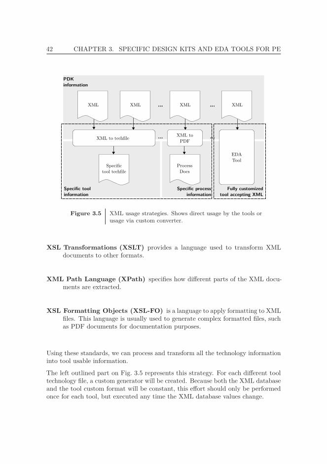
42 CHAPTER 3. SPECIFIC DESIGN KITS AND EDA TOOLS FOR PE
Speci c toolinformation
Speci c processinformation
XML XML XML
XML toPDFXML to tech le
Speci ctool tech le
ProcessDocs
PDK information
Fully customizedtool accepting XML
XML
EDATool
Figure 3.5 XML usage strategies. Shows direct usage by the tools orusage via custom converter.
XSL Transformations (XSLT) provides a language used to transform XMLdocuments to other formats.
XML Path Language (XPath) specifies how different parts of the XML docu-ments are extracted.
XSL Formatting Objects (XSL-FO) is a language to apply formatting to XMLfiles. This language is usually used to generate complex formatted files, suchas PDF documents for documentation purposes.
Using these standards, we can process and transform all the technology informationinto tool usable information.
The left outlined part on Fig. 3.5 represents this strategy. For each different tooltechnology file, a custom generator will be created. Because both the XML databaseand the tool custom format will be constant, this effort should only be performedonce for each tool, but executed any time the XML database values change.
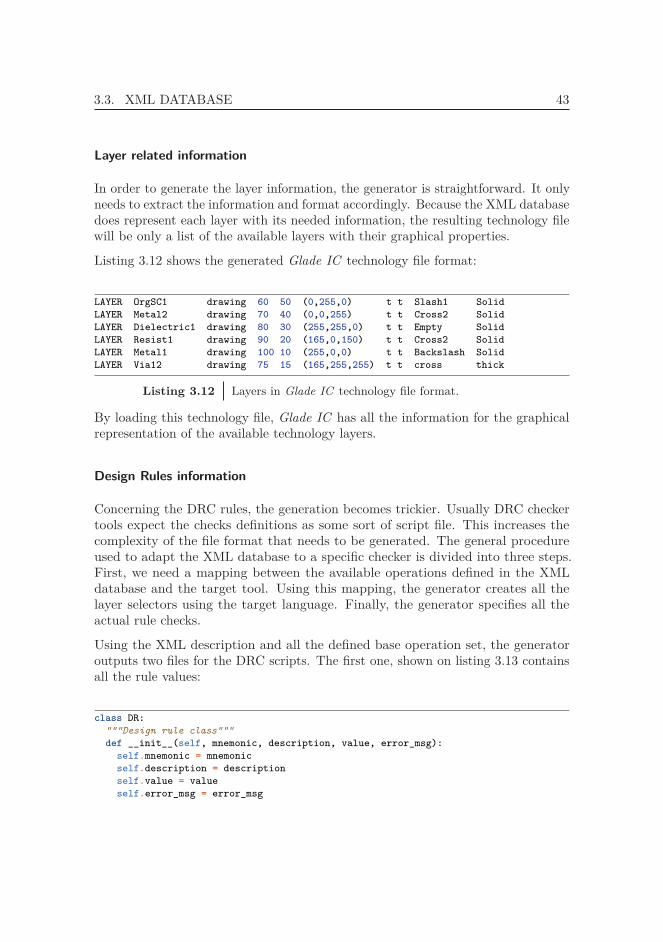
3.3. XML DATABASE 43
Layer related information
In order to generate the layer information, the generator is straightforward. It onlyneeds to extract the information and format accordingly. Because the XML databasedoes represent each layer with its needed information, the resulting technology filewill be only a list of the available layers with their graphical properties.
Listing 3.12 shows the generated Glade IC technology file format:
LAYER OrgSC1 drawing 60 50 (0,255,0) t t Slash1 SolidLAYER Metal2 drawing 70 40 (0,0,255) t t Cross2 SolidLAYER Dielectric1 drawing 80 30 (255,255,0) t t Empty SolidLAYER Resist1 drawing 90 20 (165,0,150) t t Cross2 SolidLAYER Metal1 drawing 100 10 (255,0,0) t t Backslash SolidLAYER Via12 drawing 75 15 (165,255,255) t t cross thick
Listing 3.12 Layers in Glade IC technology file format.
By loading this technology file, Glade IC has all the information for the graphicalrepresentation of the available technology layers.
Design Rules information
Concerning the DRC rules, the generation becomes trickier. Usually DRC checkertools expect the checks definitions as some sort of script file. This increases thecomplexity of the file format that needs to be generated. The general procedureused to adapt the XML database to a specific checker is divided into three steps.First, we need a mapping between the available operations defined in the XMLdatabase and the target tool. Using this mapping, the generator creates all thelayer selectors using the target language. Finally, the generator specifies all theactual rule checks.
Using the XML description and all the defined base operation set, the generatoroutputs two files for the DRC scripts. The first one, shown on listing 3.13 containsall the rule values:
class DR:"""Design rule class"""def __init__(self, mnemonic, description, value, error_msg):
self.mnemonic = mnemonicself.description = descriptionself.value = valueself.error_msg = error_msg
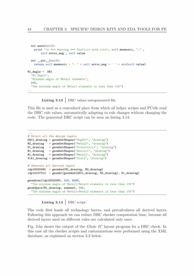
44 CHAPTER 3. SPECIFIC DESIGN KITS AND EDA TOOLS FOR PE
def warn(self):print "\n *** Warning *** Conflict with rule", self.mnemonic, ":" ,
self.error_msg , self.value
def __str__(self):return self.mnemonic + ": " + self.error_msg + ’ ’ + str(self.value)
M1_Angle = DR("M1.Angle","Minimum angle of Metal1 elements",100,"The minimum angle of Metal1 elements is less than 100")
...
Listing 3.13 DRC values autogenerated file.
This file is used as a centralized place from which all helper scripts and PCells readthe DRC rule values, automatically adapting to rule changes without changing thecode. The generated DRC script can be seen on listing 3.14:
...# Select all the design layersOSC1_drawing = geomGetShapes("OrgSC1", "drawing")M2_drawing = geomGetShapes("Metal2", "drawing")D1_drawing = geomGetShapes("Dielectric1", "drawing")R1_drawing = geomGetShapes("Resist1", "drawing")M1_drawing = geomGetShapes("Metal1", "drawing")VIA1_drawing = geomGetShapes("Via12", "drawing")
# Generate all derived layersidp16020080 = geomAnd(M1_drawing, M2_drawing)idp16157312 = geomOr(geomAnd(OSC1_drawing, M2_drawing), D1_drawing)...geomArea(idp16020080, 100, 9e99,
"The minimum angle of Metal1-Metal2 elements is less than 100")geomSpace(M1_drawing, samenet, 100,
"The minimum angle of Metal1-Metal2 elements is less than 100")
Listing 3.14 DRC script.
The code first loads all technology layers, and precalculates all derived layers.Following this approach we can reduce DRC checker computation time, because allderived layers used on different rules are calculated only once.
Fig. 3.6a shows the output of the Glade IC layout program for a DRC check. Inthis case all the checker scripts and customizations were performed using the XMLdatabase, as explained on section 3.3 below.
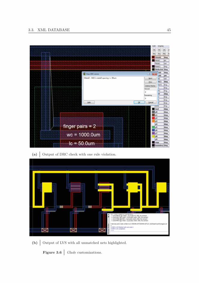
3.3. XML DATABASE 45
(a) Output of DRC check with one rule violation.
(b) Output of LVS with all unmatched nets highlighted.
Figure 3.6 Glade customizations.
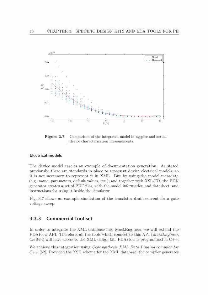
46 CHAPTER 3. SPECIFIC DESIGN KITS AND EDA TOOLS FOR PE
−15 −10 −5 0 5 10 15Vg[V]
0.0
0.5
1.0
1.5
2.0
I d[A]
×10−4
ModelMeasured
Figure 3.7 Comparison of the integrated model in ngspice and actualdevice characterization measurements.
Electrical models
The device model case is an example of documentation generation. As statedpreviously, there are standards in place to represent device electrical models, soit is not necessary to represent it in XML. But by using the model metadata(e.g. name, parameters, default values, etc.), and together with XSL-FO, the PDKgenerator creates a set of PDF files, with the model information and datasheet, andinstructions for using it inside the simulator.
Fig. 3.7 shows an example simulation of the transistor drain current for a gatevoltage sweep.
3.3.3 Commercial tool set
In order to integrate the XML database into MaskEngineer, we will extend thePDAFlow API. Therefore, all the tools which connect to this API (MaskEngineer,CleWin) will have access to the XML design kit. PDAFlow is programmed in C++.
We achieve this integration using Codesynthesis XML Data Binding compiler forC++ [62]. Provided the XSD schema for the XML database, the compiler generates
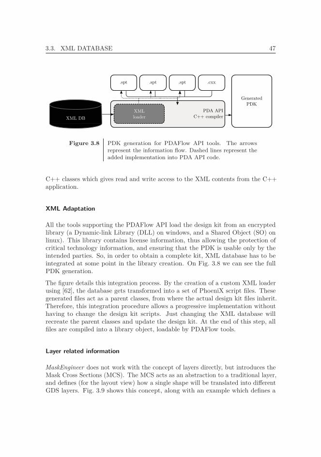
3.3. XML DATABASE 47
.spt
XML DB
GeneratedPDK
PDA APIC++ compiler
XMLloader
.spt .spt .cxx
Figure 3.8 PDK generation for PDAFlow API tools. The arrowsrepresent the information flow. Dashed lines represent theadded implementation into PDA API code.
C++ classes which gives read and write access to the XML contents from the C++application.
XML Adaptation
All the tools supporting the PDAFlow API load the design kit from an encryptedlibrary (a Dynamic-link Library (DLL) on windows, and a Shared Object (SO) onlinux). This library contains license information, thus allowing the protection ofcritical technology information, and ensuring that the PDK is usable only by theintended parties. So, in order to obtain a complete kit, XML database has to beintegrated at some point in the library creation. On Fig. 3.8 we can see the fullPDK generation.
The figure details this integration process. By the creation of a custom XML loaderusing [62], the database gets transformed into a set of PhoeniX script files. Thesegenerated files act as a parent classes, from where the actual design kit files inherit.Therefore, this integration procedure allows a progressive implementation withouthaving to change the design kit scripts. Just changing the XML database willrecreate the parent classes and update the design kit. At the end of this step, allfiles are compiled into a library object, loadable by PDAFlow tools.
Layer related information
MaskEngineer does not work with the concept of layers directly, but introduces theMask Cross Sections (MCS). The MCS acts as an abstraction to a traditional layer,and defines (for the layout view) how a single shape will be translated into differentGDS layers. Fig. 3.9 shows this concept, along with an example which defines a
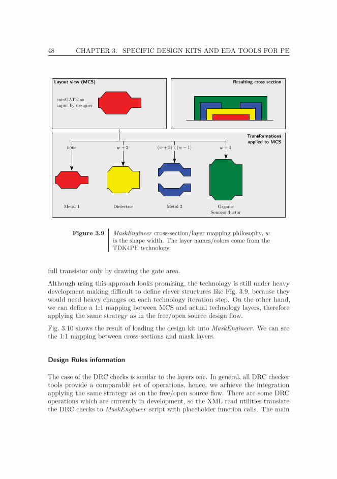
48 CHAPTER 3. SPECIFIC DESIGN KITS AND EDA TOOLS FOR PE
Layout view (MCS)
mcsGATE asinput by designer
Resulting cross section
Transformationsapplied to MCS
Metal 1 Dielectric Metal 2 OrganicSemiconductor
Figure 3.9 MaskEngineer cross-section/layer mapping philosophy, wis the shape width. The layer names/colors come from theTDK4PE technology.
full transistor only by drawing the gate area.
Although using this approach looks promising, the technology is still under heavydevelopment making difficult to define clever structures like Fig. 3.9, because theywould need heavy changes on each technology iteration step. On the other hand,we can define a 1:1 mapping between MCS and actual technology layers, thereforeapplying the same strategy as in the free/open source design flow.
Fig. 3.10 shows the result of loading the design kit into MaskEngineer. We can seethe 1:1 mapping between cross-sections and mask layers.
Design Rules information
The case of the DRC checks is similar to the layers one. In general, all DRC checkertools provide a comparable set of operations, hence, we achieve the integrationapplying the same strategy as on the free/open source flow. There are some DRCoperations which are currently in development, so the XML read utilities translatethe DRC checks to MaskEngineer script with placeholder function calls. The main
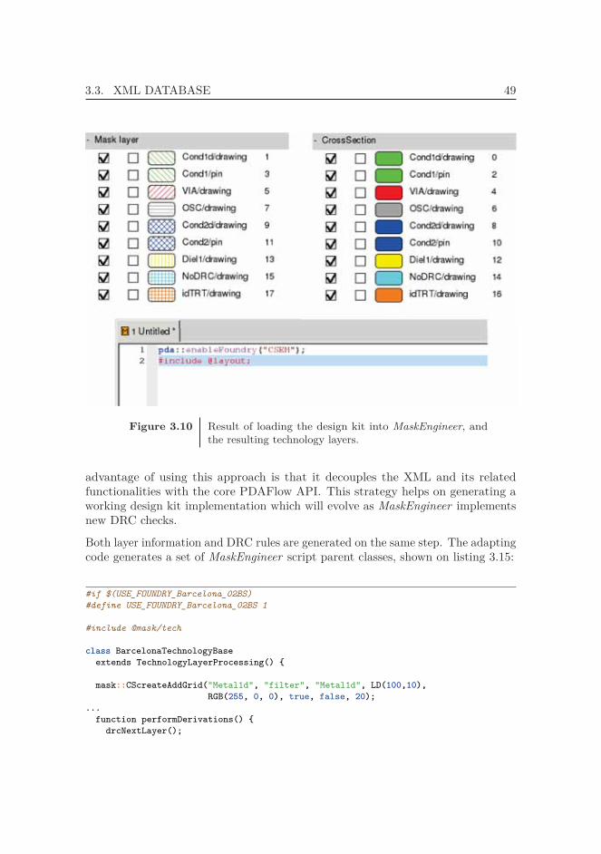
3.3. XML DATABASE 49
Figure 3.10 Result of loading the design kit into MaskEngineer, andthe resulting technology layers.
advantage of using this approach is that it decouples the XML and its relatedfunctionalities with the core PDAFlow API. This strategy helps on generating aworking design kit implementation which will evolve as MaskEngineer implementsnew DRC checks.
Both layer information and DRC rules are generated on the same step. The adaptingcode generates a set of MaskEngineer script parent classes, shown on listing 3.15:
#if $(USE_FOUNDRY_Barcelona_02BS)#define USE_FOUNDRY_Barcelona_02BS 1
#include @mask/tech
class BarcelonaTechnologyBaseextends TechnologyLayerProcessing() {
mask::CScreateAddGrid("Metal1d", "filter", "Metal1d", LD(100,10),RGB(255, 0, 0), true, false, 20);
...function performDerivations() {
drcNextLayer();
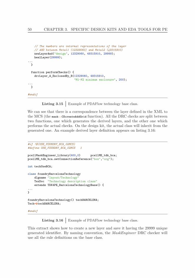
50 CHAPTER 3. SPECIFIC DESIGN KITS AND EDA TOOLS FOR PE
// The numbers are internal representations of the layer// AND between Metal1 (12329060) and Metal2 (49315910)newLayerAnd("design", 12329060, 49315910, 29999);healLayer(29999);
...}
function performChecks() {drcLayer_A_EnclosedBy_B(12329060, 49315910,
"M1-M2 minimum enclosure", 200);...
}
#endif
Listing 3.15 Example of PDAFlow technology base class.
We can see that there is a correspondence between the layer defined in the XML tothe MCS (the mask::CScreateAddGrid function). All the DRC checks are split betweentwo functions, one which generates the derived layers, and the other one whichperforms the actual checks. On the design kit, the actual class will inherit from thegenerated one. An example derived layer definition appears on listing 3.16:
#if !$(USE_FOUNDRY_BCA_02MCS)#define USE_FOUNDRY_BCA_02MCS 1
pcellMaskEngineer_Library(400,0) pcellME_tdk_bca;pcellME_tdk_bca.setConnectionReference("box","org");
int techUseBCA;
class foundryBarcelonaTechnologydlgname "layout/Technology"TexDoc "Technology description class"extends TDK4PE_BarcelonaTechnologyBase() {
...}
foundryBarcelonaTechnology() techBARCELONA;Tech=&techBARCELONA;
#endif
Listing 3.16 Example of PDAFlow technology base class.
This extract shows how to create a new layer and save it having the 29999 uniquegenerated identifier. By naming convention, the MaskEngineer DRC checker willuse all the rule definitions on the base class.
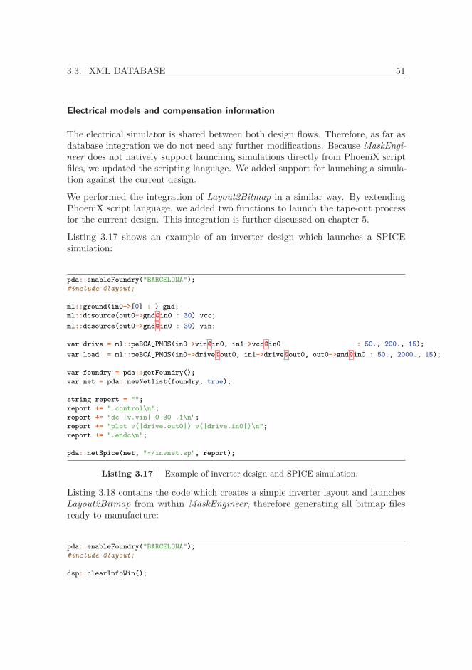
3.3. XML DATABASE 51
Electrical models and compensation information
The electrical simulator is shared between both design flows. Therefore, as far asdatabase integration we do not need any further modifications. Because MaskEngi-neer does not natively support launching simulations directly from PhoeniX scriptfiles, we updated the scripting language. We added support for launching a simula-tion against the current design.
We performed the integration of Layout2Bitmap in a similar way. By extendingPhoeniX script language, we added two functions to launch the tape-out processfor the current design. This integration is further discussed on chapter 5.
Listing 3.17 shows an example of an inverter design which launches a SPICEsimulation:
pda::enableFoundry("BARCELONA");#include @layout;
ml::ground(in0->[0] : ) gnd;ml::dcsource(out0->gnd@in0 : 30) vcc;ml::dcsource(out0->gnd@in0 : 30) vin;
var drive = ml::peBCA_PMOS(in0->vin@in0, in1->vcc@in0 : 50., 200., 15);var load = ml::peBCA_PMOS(in0->drive@out0, in1->drive@out0, out0->gnd@in0 : 50., 2000., 15);
var foundry = pda::getFoundry();var net = pda::newNetlist(foundry, true);
string report = "";report += ".control\n";report += "dc |v.vin| 0 30 .1\n";report += "plot v(|drive.out0|) v(|drive.in0|)\n";report += ".endc\n";
pda::netSpice(net, "~/invnet.sp", report);
Listing 3.17 Example of inverter design and SPICE simulation.
Listing 3.18 contains the code which creates a simple inverter layout and launchesLayout2Bitmap from within MaskEngineer, therefore generating all bitmap filesready to manufacture:
pda::enableFoundry("BARCELONA");#include @layout;
dsp::clearInfoWin();
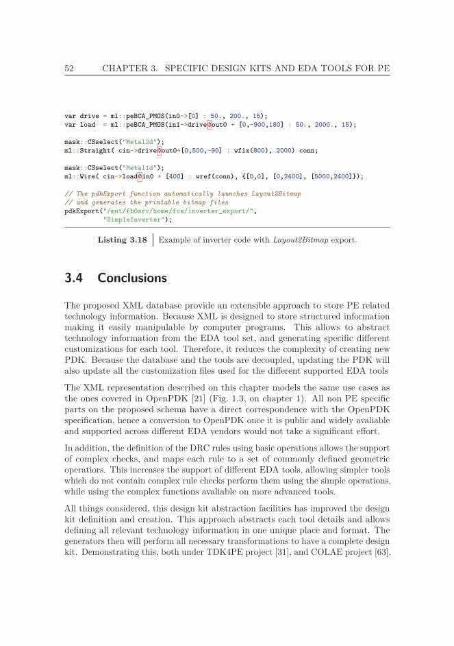
52 CHAPTER 3. SPECIFIC DESIGN KITS AND EDA TOOLS FOR PE
var drive = ml::peBCA_PMOS(in0->[0] : 50., 200., 15);var load = ml::peBCA_PMOS(in1->drive@out0 + [0,-900,180] : 50., 2000., 15);
mask::CSselect("Metal2d");ml::Straight( cin->drive@out0+[0,500,-90] : wfix(800), 2000) conn;
mask::CSselect("Metal1d");ml::Wire( cin->load@in0 + [400] : wref(conn), {[0,0], [0,2400], [5000,2400]});
// The pdkExport function automatically launches Layout2Bitmap// and generates the printable bitmap filespdkExport("/mnt/fb0srv/home/fva/inverter_export/",
"SimpleInverter");
Listing 3.18 Example of inverter code with Layout2Bitmap export.
3.4 Conclusions
The proposed XML database provide an extensible approach to store PE relatedtechnology information. Because XML is designed to store structured informationmaking it easily manipulable by computer programs. This allows to abstracttechnology information from the EDA tool set, and generating specific differentcustomizations for each tool. Therefore, it reduces the complexity of creating newPDK. Because the database and the tools are decoupled, updating the PDK willalso update all the customization files used for the different supported EDA tools
The XML representation described on this chapter models the same use cases asthe ones covered in OpenPDK [21] (Fig. 1.3, on chapter 1). All non PE specificparts on the proposed schema have a direct correspondence with the OpenPDKspecification, hence a conversion to OpenPDK once it is public and widely avaliableand supported across different EDA vendors would not take a significant effort.
In addition, the definition of the DRC rules using basic operations allows the supportof complex checks, and maps each rule to a set of commonly defined geometricoperatiors. This increases the support of different EDA tools, allowing simpler toolswhich do not contain complex rule checks perform them using the simple operations,while using the complex functions avaliable on more advanced tools.
All things considered, this design kit abstraction facilities has improved the designkit definition and creation. This approach abstracts each tool details and allowsdefining all relevant technology information in one unique place and format. Thegenerators then will perform all necessary transformations to have a complete designkit. Demonstrating this, both under TDK4PE project [31], and COLAE project [63],

3.4. CONCLUSIONS 53
we managed to create two different design kits for two different technologies. Usingthe XML database and the generators, we were able to obtain a design kit for bothtechnologies and for both set of tools from one unique representation in a very shortperiod of time: less than two months from initial contact with the foundries withless than three weeks of technical work, including the a few PCells development foreach technology. This demonstrates the efficiency of the proposed approach.
To show the usefulness of having this abstract representation of technology informa-tion, two different sets of EDA tools have been customized for the use of this PDK,providing a direct path from design to manufacturable designs from both of thesetool sets.

Image based technologycharacterization 4
After knowing which information is required for a PDK, and which tools coverthe design flow, we need procedures to extract critical technology information.Following the presented design flow, the last missing step is the tape-out processwhich will finally bridge the gap between design and manufacturing. To extract thenecessary information, it is essential to develop a new characterization procedure,study ink behavior and extract the FEC rules.
This chapter explains how the experiments to obtain those compensations aregenerated automatically, and the set of analysis performed on extracted data. Overthe rest of this chapter we will present the full analysis framework along with severalcase studies, ranging from FEC rules extraction to process quality control andcharacterization.
4.1 Experimental approach
Throughout the TDK4PE and ASPEC-TDK projects we have found that in theprocess of inkjet printing there is no proper knowledge about the dynamics of fluids,their interaction with the substrates, or the mechanical and thermal effects of theseprocesses. This knowledge is necessary to anticipate suitable compensation strategieswhich ensure that the morphology of the layer conforms to the expectations of thedesigned one. Although our own knowledge is far away from those topics, but wecan extract from our know-how in microelectronics which are the main shapes andstructures where compensations are critical.
55
56 CHAPTER 4. IMAGE BASED TECHNOLOGY CHARACTERIZATION
Due to this fact we decided to approach the characterization in a proactive way by:
1. Providing a basic set of critical shapes and structures to study compensationneeds and effects.
2. Define different compensation strategies (shapes modifications and fillingpatterns at bitmap level) based on past experimental observations.
3. Produce automatically thousands printed structures with and without differentcompensation strategies.
4. Characterize such large amount of structures by means of a semiautomaticsetup applying electrical tests and image capture.
5. Perform image processing and statistical data analysis on the different results.
6. Extract conclusions on two complementary directions: compensation strategiesand rules as well as information about printing process quality to improve itscontrol and accuracy.
Fig 4.1 summarizes this characterization approach used to fix compensation tech-niques without an in-deep knowledge on the fluidic effects and their related models.
4.1.1 Experiment generation
The automated layout procedures section on Fig. 4.1, is the responsible of generatingthe layout. To perform the generation, it uses the concept of PCells. A PCell is apiece of code which, when executed, will generate a particular layout depending onits parameters.
Together with a scriptable EDA tool, we can develop a script which will automatePCell execution, and therefore, generate a full layout.
To obtain the final design, this script will read a configuration file specifying all theexperiment constraints. This includes which type of samples will be used, whichPCell parameters will vary, and their range values (for example the sample sizesand orientation), the desired number of repetitions, and several physical parameterssuch as the foil and sample dimensions.
With this information the script will generate all combinations and repetitions ofthe samples and perform a random permutation of these generated combinations,arranging the samples across the foil, and saving the used random seed. This laststep is very important for experiment repeatability. At the end of the generation
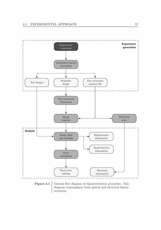
4.1. EXPERIMENTAL APPROACH 57
Final scoreranking
Image alignand cleaning
Imagecapture
PrintabledesignTest images Test structures
position le
Experimentconstrains
Automated layoutprocedures
Test strcuturesfabrication
Displacementinformation
Scorecalculation
Small featuresinformation
Electricaltests
Electricalinformation
Experimentgeneration
Analysis
Figure 4.1 General flow diagram of characterization procedure. Thisdiagram contemplates both optical and electrical charac-terization.
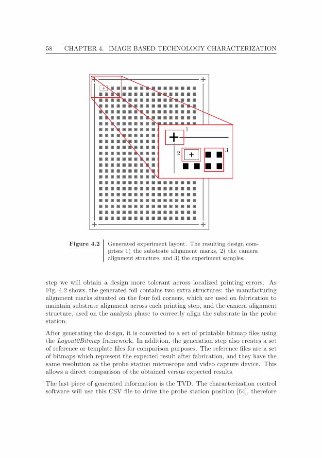
58 CHAPTER 4. IMAGE BASED TECHNOLOGY CHARACTERIZATION
1
2 3
Figure 4.2 Generated experiment layout. The resulting design com-prises 1) the substrate alignment marks, 2) the cameraalignment structure, and 3) the experiment samples.
step we will obtain a design more tolerant across localized printing errors. AsFig. 4.2 shows, the generated foil contains two extra structures: the manufacturingalignment marks situated on the four foil corners, which are used on fabrication tomaintain substrate alignment across each printing step, and the camera alignmentstructure, used on the analysis phase to correctly align the substrate in the probestation.
After generating the design, it is converted to a set of printable bitmap files usingthe Layout2Bitmap framework. In addition, the generation step also creates a setof reference or template files for comparison purposes. The reference files are a setof bitmaps which represent the expected result after fabrication, and they have thesame resolution as the probe station microscope and video capture device. Thisallows a direct comparison of the obtained versus expected results.
The last piece of generated information is the TVD. The characterization controlsoftware will use this CSV file to drive the probe station position [64], therefore
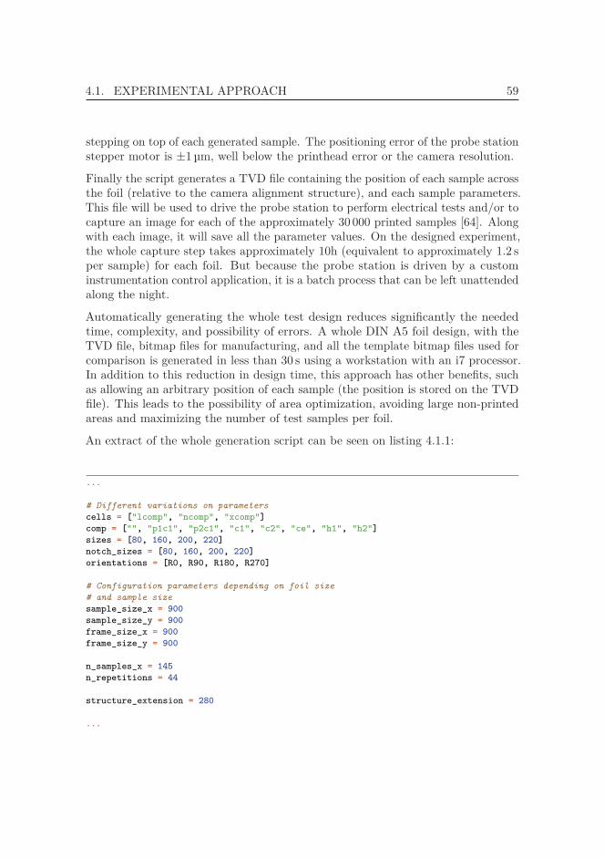
4.1. EXPERIMENTAL APPROACH 59
stepping on top of each generated sample. The positioning error of the probe stationstepper motor is ±1 μm, well below the printhead error or the camera resolution.
Finally the script generates a TVD file containing the position of each sample acrossthe foil (relative to the camera alignment structure), and each sample parameters.This file will be used to drive the probe station to perform electrical tests and/or tocapture an image for each of the approximately 30 000 printed samples [64]. Alongwith each image, it will save all the parameter values. On the designed experiment,the whole capture step takes approximately 10h (equivalent to approximately 1.2 sper sample) for each foil. But because the probe station is driven by a custominstrumentation control application, it is a batch process that can be left unattendedalong the night.
Automatically generating the whole test design reduces significantly the neededtime, complexity, and possibility of errors. A whole DIN A5 foil design, with theTVD file, bitmap files for manufacturing, and all the template bitmap files used forcomparison is generated in less than 30 s using a workstation with an i7 processor.In addition to this reduction in design time, this approach has other benefits, suchas allowing an arbitrary position of each sample (the position is stored on the TVDfile). This leads to the possibility of area optimization, avoiding large non-printedareas and maximizing the number of test samples per foil.
An extract of the whole generation script can be seen on listing 4.1.1:
...
# Different variations on parameterscells = ["lcomp", "ncomp", "xcomp"]comp = ["", "p1c1", "p2c1", "c1", "c2", "ce", "h1", "h2"]sizes = [80, 160, 200, 220]notch_sizes = [80, 160, 200, 220]orientations = [R0, R90, R180, R270]
# Configuration parameters depending on foil size# and sample sizesample_size_x = 900sample_size_y = 900frame_size_x = 900frame_size_y = 900
n_samples_x = 145n_repetitions = 44
structure_extension = 280
...
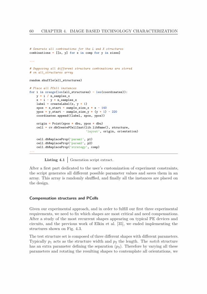
60 CHAPTER 4. IMAGE BASED TECHNOLOGY CHARACTERIZATION
# Generate all combinations for the L and X structurescombinations = [[x, y] for x in comp for y in sizes]
...
# Supposing all different structure combinations are stored# on all_structures array
random.shuffle(all_structures)
# Place all PCell instancesfor i in xrange(len(all_structures) - len(coordinates)):
y = i / n_samples_xx = i - y * n_samples_xlabel = createLabel(x, y + 1)xpos = x_start + sample_size_x * x - 140ypos = y_start - sample_size_y * (y + 1) - 220coordinates.append((label, xpos, ypos))
origin = Point(xpos * dbu, ypos * dbu)cell = cv.dbCreatePCellInst(lib.libName(), structure,
’layout’, origin, orientation)
cell.dbReplaceProp(’param1’, p1)cell.dbReplaceProp(’param2’, p2)cell.dbReplaceProp(’strategy’, comp)
...
Listing 4.1 Generation script extract.
After a first part dedicated to the user’s customization of experiment constraints,the script generates all different possible parameter values and saves them in anarray. This array is randomly shuffled, and finally all the instances are placed onthe design.
Compensation structures and PCells
Given our experimental approach, and in order to fulfill our first three experimentalrequirements, we need to fix which shapes are most critical and need compensations.After a study of the most recurrent shapes appearing on typical PE devices andcircuits, and the previous work of Elkin et al. [35], we ended implementing thestructures shown on Fig. 4.3.
The test structure set is composed of three different shapes with different parameters.Typically p1 acts as the structure width and p2 the length. The notch structurehas an extra parameter defining the separation (p3). Therefore by varying all theseparameters and rotating the resulting shapes to contemplate all orientations, we
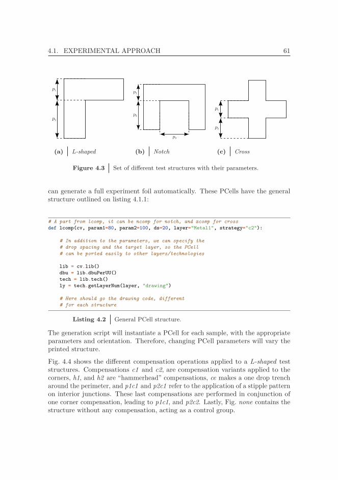
4.1. EXPERIMENTAL APPROACH 61
p1
p2
(a) L-shaped
p1
p2
p3
(b) Notch
p1
p2
(c) Cross
Figure 4.3 Set of different test structures with their parameters.
can generate a full experiment foil automatically. These PCells have the generalstructure outlined on listing 4.1.1:
# A part from lcomp, it can be ncomp for notch, and xcomp for crossdef lcomp(cv, param1=80, param2=100, ds=20, layer="Metal1", strategy="c2"):
# In addition to the parameters, we can specify the# drop spacing and the target layer, so the PCell# can be ported easily to other layers/technologies
lib = cv.lib()dbu = lib.dbuPerUU()tech = lib.tech()ly = tech.getLayerNum(layer, "drawing")
# Here should go the drawing code, different# for each structure
Listing 4.2 General PCell structure.
The generation script will instantiate a PCell for each sample, with the appropriateparameters and orientation. Therefore, changing PCell parameters will vary theprinted structure.
Fig. 4.4 shows the different compensation operations applied to a L-shaped teststructures. Compensations c1 and c2, are compensation variants applied to thecorners, h1, and h2 are “hammerhead” compensations, ce makes a one drop trencharound the perimeter, and p1c1 and p2c1 refer to the application of a stipple patternon interior junctions. These last compensations are performed in conjunction ofone corner compensation, leading to p1c1, and p2c2. Lastly, Fig. none contains thestructure without any compensation, acting as a control group.
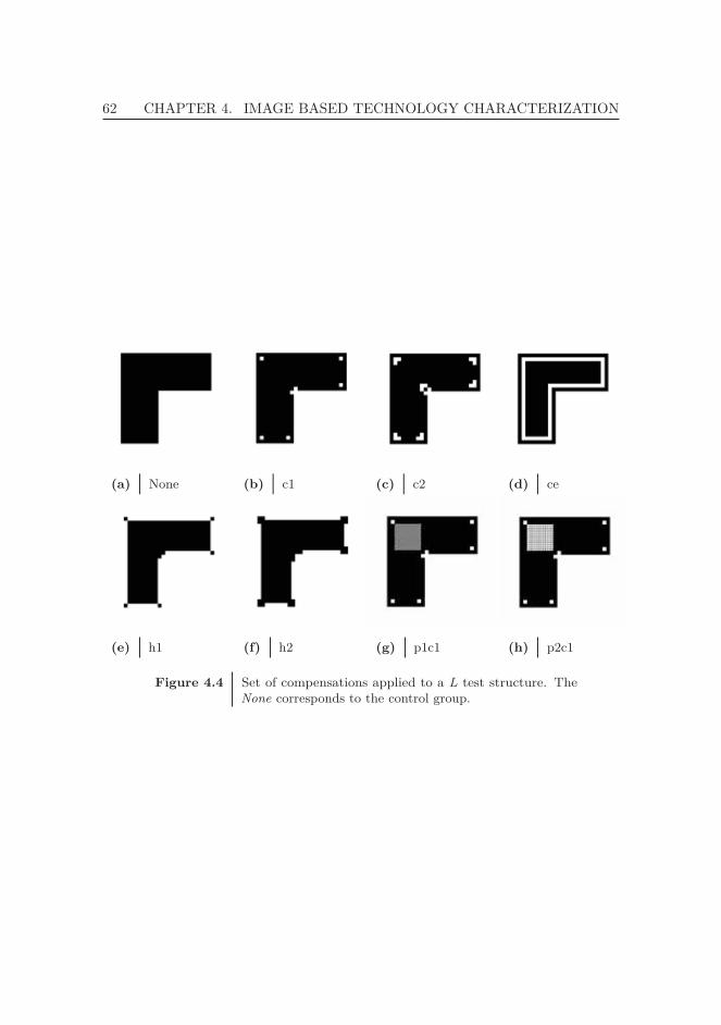
62 CHAPTER 4. IMAGE BASED TECHNOLOGY CHARACTERIZATION
(a) None (b) c1 (c) c2 (d) ce
(e) h1 (f) h2 (g) p1c1 (h) p2c1
Figure 4.4 Set of compensations applied to a L test structure. TheNone corresponds to the control group.
4.2. ANALYSIS 63
4.2 Analysis
To evaluate the printed shapes, and to extract printing parameters, the characteri-zation setup analyzes each image using a set of image processing algorithms [65].The overall procedure is to condition captures images by thresholding using Otsu’smethod [66], clean the obtained image using morphological operations [67], andalign it with the expected results using Fourier cross-correlation [68]. Once theimages are correctly prepared, we can compare them and extract similarity results.All these procedures will be detailed along this section.
Preliminary analysis on image data led us to consider studying ink spreading, teststructure misalignment, and number of detected satellite droplets in addition to thesample score. This data gives more information about process stability and possiblesubstrate curing deformations. Concerning the main points of the experimentalapproach presented on section 4.1, this section covers the last three points.
4.2.1 Image processing operations
The first step to process the captured image is to convert it to a binary image(B/W). This is performed by the Otsu algorithm [66]. This algorithm calculatesa threshold value which will best separate the image into two different regionsor classes. This method assumes that the image only has two different regions,and returns the threshold which minimizes intra-class variance, thus maximizinginter-class variance. Therefore, the obtained threshold is the optimal value whichseparates those two classes. In this case the two classes on the image are the regionswith and without ink.
In order to further condition the captured images they need to pass through acleaning process. This procedure is based on the set of morphological operations inbinary images [67, 69]: erosion, dilation, opening, and closing, and on connectedcomponent labelling [70, pp. 63-103].
Morphological operations on the captured images are done with an structuringelement, which is a shape (in our case a square centered on the origin) with a certaindimensions. Fig. 4.5 has the graphical representation of this set of operations.
The mathematical definition of these operations is as follows. Let A be the capturedimage, and B the structuring element. Then, erosion is defined as
A � B =⋂
b∈B
A−b = {z ∈ E|Bz ⊆ A}, (4.1)
64 CHAPTER 4. IMAGE BASED TECHNOLOGY CHARACTERIZATION
where Bz is the translation of B by the vector z, i.e. Bz = {b + z|b ∈ B}, ∀z ∈ E.Therefore, as Fig. 4.5a shows, the final result is the set of all points that the centerof B reaches, when moves inside A. The final result is the dark gray shaded part.
Dilation is defined as
A ⊕ B =⋃
a∈A
B = {z ∈ E|(Bs)z ∩ A = ∅}, (4.2)
where Bs is the symmetric of B, i.e. Bs = {x ∈ E| − x ∈ B}. The final result is theset of points which reaches B, when its center moves inside A. Dark gray shadedpart of Fig. 4.5b shows the resulting shape.
Then, combining equations (4.1), and (4.2), the opening is defined as
A ◦ B = (A � B) ⊕ B (4.3)
and the closing as
A • B = (A ⊕ B) � B. (4.4)
Fig. 4.5c, and 4.5d contains an example of the application of these operations.
Connected component labelling assigns an unique label to each different region ofthe image, depending on a given heuristic. Fig. 4.6 illustrates the possible heuristics.We consider that the darkest shaded pixels on the figure are 4-connected to theblack central pixel. Adding the light shaded pixels to the 4-connected ones givesthe 8-connected pixels to the black pixel.
By labelling the captured image and identifying uniquely different connected regions,we can query each part for different values such as the perimeter or the area, thusfacilitating the detection of satellite drops.
Printing quality
In the case of our captured images, the opening and closing operations, on eqs. (4.3),and (4.4) respectively, are very important, because they allow the removal of smalldark and light features respectively. By performing an opening and a closing, wecan eliminate features which are smaller than the structuring element size, hencedetecting satellite drops. Then number of eliminated features therefore is a goodindicator of printing quality.
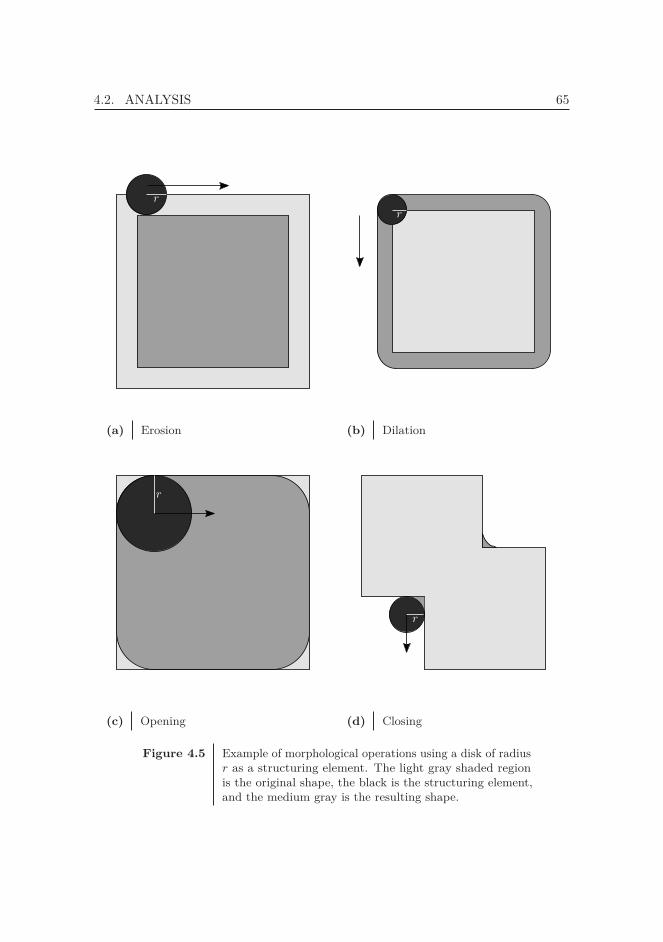
4.2. ANALYSIS 65
(a) Erosion (b) Dilation
(c) Opening (d) Closing
Figure 4.5 Example of morphological operations using a disk of radiusr as a structuring element. The light gray shaded regionis the original shape, the black is the structuring element,and the medium gray is the resulting shape.
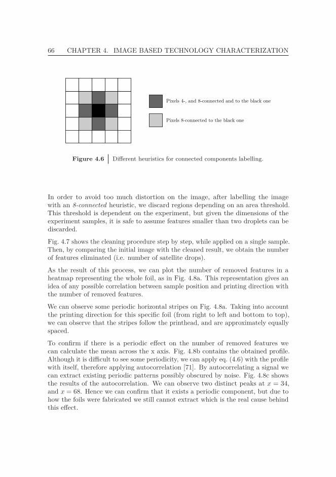
66 CHAPTER 4. IMAGE BASED TECHNOLOGY CHARACTERIZATION
Pixels 4-, and 8-connected and to the black one
Pixels 8-connected to the black one
Figure 4.6 Different heuristics for connected components labelling.
In order to avoid too much distortion on the image, after labelling the imagewith an 8-connected heuristic, we discard regions depending on an area threshold.This threshold is dependent on the experiment, but given the dimensions of theexperiment samples, it is safe to assume features smaller than two droplets can bediscarded.
Fig. 4.7 shows the cleaning procedure step by step, while applied on a single sample.Then, by comparing the initial image with the cleaned result, we obtain the numberof features eliminated (i.e. number of satellite drops).
As the result of this process, we can plot the number of removed features in aheatmap representing the whole foil, as in Fig. 4.8a. This representation gives anidea of any possible correlation between sample position and printing direction withthe number of removed features.
We can observe some periodic horizontal stripes on Fig. 4.8a. Taking into accountthe printing direction for this specific foil (from right to left and bottom to top),we can observe that the stripes follow the printhead, and are approximately equallyspaced.
To confirm if there is a periodic effect on the number of removed features wecan calculate the mean across the x axis. Fig. 4.8b contains the obtained profile.Although it is difficult to see some periodicity, we can apply eq. (4.6) with the profilewith itself, therefore applying autocorrelation [71]. By autocorrelating a signal wecan extract existing periodic patterns possibly obscured by noise. Fig. 4.8c showsthe results of the autocorrelation. We can observe two distinct peaks at x = 34,and x = 68. Hence we can confirm that it exists a periodic component, but due tohow the foils were fabricated we still cannot extract which is the real cause behindthis effect.
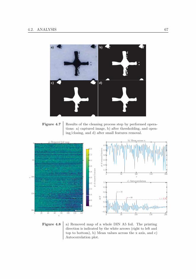
4.2. ANALYSIS 67
a) b)
c) d)
Figure 4.7 Results of the cleaning process step by performed opera-tions: a) captured image, b) after thresholding, and open-ing/closing, and d) after small features removal.
0 20 40 60 80 100 120 140x
0
50
100
150
200
y
a) Removed foil map
0 50 100 150 200y
1.5
2.0
2.5
3.0
3.5
4.0
#of
removed
features
b) Mean across x
0 50 100 150 200
−0.2
0.0
0.2
0.4
0.6
0.8
1.0
ACF
x = 34
x = 68 t = 0.30
c) Autocorrelation
0.0
0.8
1.6
2.4
3.2
4.0
4.8
5.6
6.4
7.2
8.0
#of
removed
features
Figure 4.8 a) Removed map of a whole DIN A5 foil. The printingdirection is indicated by the white arrows (right to left andtop to bottom), b) Mean values across the x axis, and c)Autocorrelation plot.
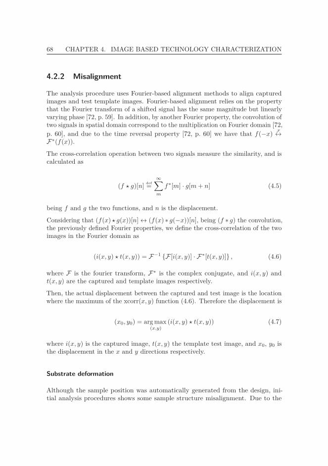
68 CHAPTER 4. IMAGE BASED TECHNOLOGY CHARACTERIZATION
4.2.2 Misalignment
The analysis procedure uses Fourier-based alignment methods to align capturedimages and test template images. Fourier-based alignment relies on the propertythat the Fourier transform of a shifted signal has the same magnitude but linearlyvarying phase [72, p. 59]. In addition, by another Fourier property, the convolution oftwo signals in spatial domain correspond to the multiplication on Fourier domain [72,p. 60], and due to the time reversal property [72, p. 60] we have that f(−x) F↔F∗(f(x)).
The cross-correlation operation between two signals measure the similarity, and iscalculated as
(f � g)[n] def=∞∑m
f∗[m] · g[m + n] (4.5)
being f and g the two functions, and n is the displacement.
Considering that (f(x) � g(x))[n] ↔ (f(x) ∗ g(−x))[n], being (f ∗ g) the convolution,the previously defined Fourier properties, we define the cross-correlation of the twoimages in the Fourier domain as
(i(x, y) � t(x, y)) = F−1 {F [i(x, y)] · F∗[t(x, y)]} , (4.6)
where F is the fourier transform, F∗ is the complex conjugate, and i(x, y) andt(x, y) are the captured and template images respectively.
Then, the actual displacement between the captured and test image is the locationwhere the maximum of the xcorr(x, y) function (4.6). Therefore the displacement is
(x0, y0) = arg max(x,y)
(i(x, y) � t(x, y)) (4.7)
where i(x, y) is the captured image, t(x, y) the template test image, and x0, y0 isthe displacement in the x and y directions respectively.
Substrate deformation
Although the sample position was automatically generated from the design, ini-tial analysis procedures shows some sample structure misalignment. Due to the
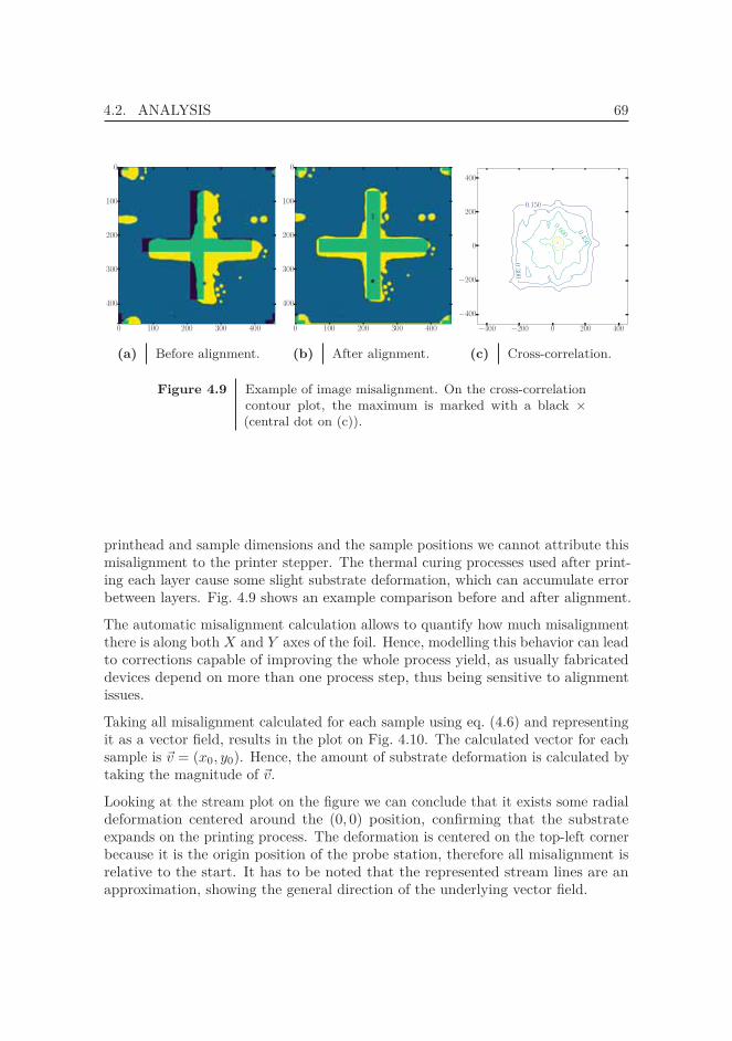
4.2. ANALYSIS 69
0 100 200 300 400
0
100
200
300
400
(a) Before alignment.
0 100 200 300 400
0
100
200
300
400
(b) After alignment.
−400 −200 0 200 400
−400
−200
0
200
400
0.1500.300
0.450
0.600
(c) Cross-correlation.
Figure 4.9 Example of image misalignment. On the cross-correlationcontour plot, the maximum is marked with a black ×(central dot on (c)).
printhead and sample dimensions and the sample positions we cannot attribute thismisalignment to the printer stepper. The thermal curing processes used after print-ing each layer cause some slight substrate deformation, which can accumulate errorbetween layers. Fig. 4.9 shows an example comparison before and after alignment.
The automatic misalignment calculation allows to quantify how much misalignmentthere is along both X and Y axes of the foil. Hence, modelling this behavior can leadto corrections capable of improving the whole process yield, as usually fabricateddevices depend on more than one process step, thus being sensitive to alignmentissues.
Taking all misalignment calculated for each sample using eq. (4.6) and representingit as a vector field, results in the plot on Fig. 4.10. The calculated vector for eachsample is �v = (x0, y0). Hence, the amount of substrate deformation is calculated bytaking the magnitude of �v.
Looking at the stream plot on the figure we can conclude that it exists some radialdeformation centered around the (0, 0) position, confirming that the substrateexpands on the printing process. The deformation is centered on the top-left cornerbecause it is the origin position of the probe station, therefore all misalignment isrelative to the start. It has to be noted that the represented stream lines are anapproximation, showing the general direction of the underlying vector field.
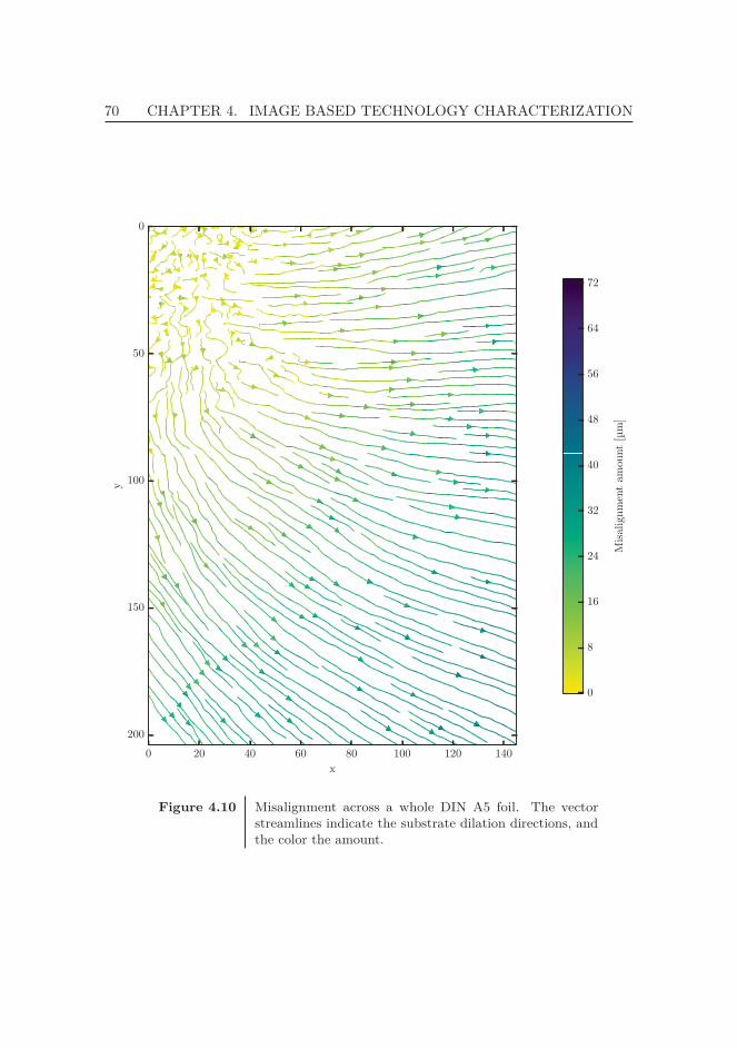
70 CHAPTER 4. IMAGE BASED TECHNOLOGY CHARACTERIZATION
0 20 40 60 80 100 120 140
x
0
50
100
150
200
y
0
8
16
24
32
40
48
56
64
72
Misalignmentam
ount[μm]
Figure 4.10 Misalignment across a whole DIN A5 foil. The vectorstreamlines indicate the substrate dilation directions, andthe color the amount.
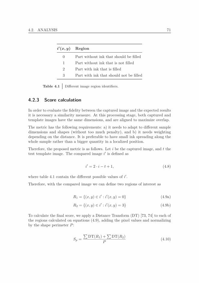
4.2. ANALYSIS 71
i′(x, y) Region
0 Part without ink that should be filled1 Part without ink that is not filled2 Part with ink that is filled3 Part with ink that should not be filled
Table 4.1 Different image region identifiers.
4.2.3 Score calculation
In order to evaluate the fidelity between the captured image and the expected resultsit is necessary a similarity measure. At this processing stage, both captured andtemplate images have the same dimensions, and are aligned to maximize overlap.
The metric has the following requirements: a) it needs to adapt to different sampledimensions and shapes (without too much penalty), and b) it needs weightingdepending on the distance. It is preferable to have small ink spreading along thewhole sample rather than a bigger quantity in a localized position.
Therefore, the proposed metric is as follows. Let i be the captured image, and t thetest template image. The compared image i′ is defined as
i′ = 2 · i − t + 1, (4.8)
where table 4.1 contain the different possible values of i′.
Therefore, with the compared image we can define two regions of interest as
R1 = {(x, y) ∈ i′ : i′(x, y) = 0} (4.9a)
R2 = {(x, y) ∈ i′ : i′(x, y) = 3} (4.9b)
To calculate the final score, we apply a Distance Transform (DT) [73, 74] to each ofthe regions calculated on equations (4.9), adding the pixel values and normalizingby the shape perimeter P :
Sp =∑
DT(R1) +∑
DT(R2)P
(4.10)
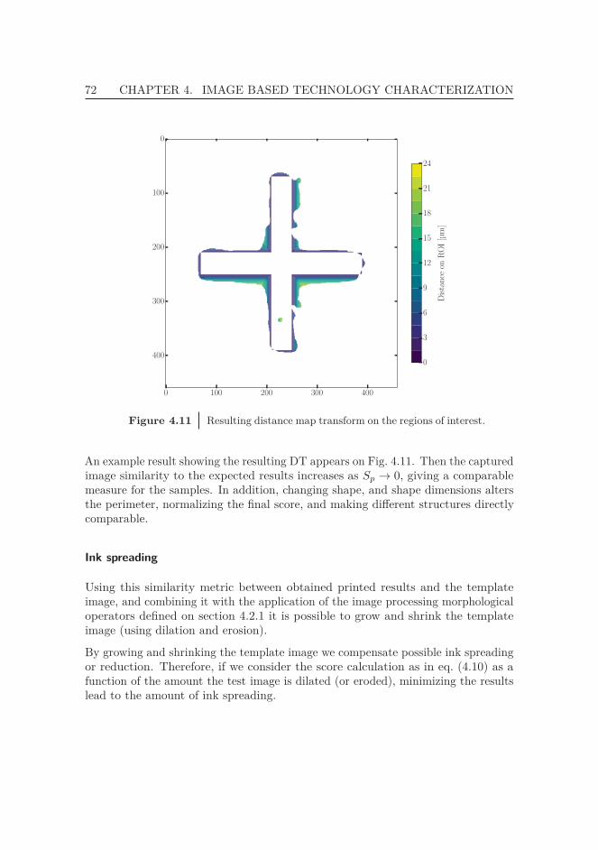
72 CHAPTER 4. IMAGE BASED TECHNOLOGY CHARACTERIZATION
0 100 200 300 400
0
100
200
300
4000
3
6
9
12
15
18
21
24
Distance
onROI[μm]
Figure 4.11 Resulting distance map transform on the regions of interest.
An example result showing the resulting DT appears on Fig. 4.11. Then the capturedimage similarity to the expected results increases as Sp → 0, giving a comparablemeasure for the samples. In addition, changing shape, and shape dimensions altersthe perimeter, normalizing the final score, and making different structures directlycomparable.
Ink spreading
Using this similarity metric between obtained printed results and the templateimage, and combining it with the application of the image processing morphologicaloperators defined on section 4.2.1 it is possible to grow and shrink the templateimage (using dilation and erosion).
By growing and shrinking the template image we compensate possible ink spreadingor reduction. Therefore, if we consider the score calculation as in eq. (4.10) as afunction of the amount the test image is dilated (or eroded), minimizing the resultslead to the amount of ink spreading.
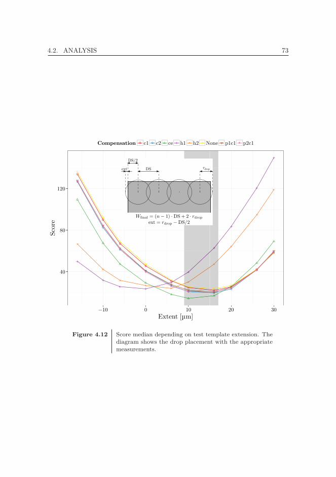
4.2. ANALYSIS 73
40
80
120
10 0 10 20 30Extent [μm]
Scor
e
Compensation c1 c2 ce h1 h2 None p1c1 p2c1
rdrop
DS/2
ext DS
Figure 4.12 Score median depending on test template extension. Thediagram shows the drop placement with the appropriatemeasurements.
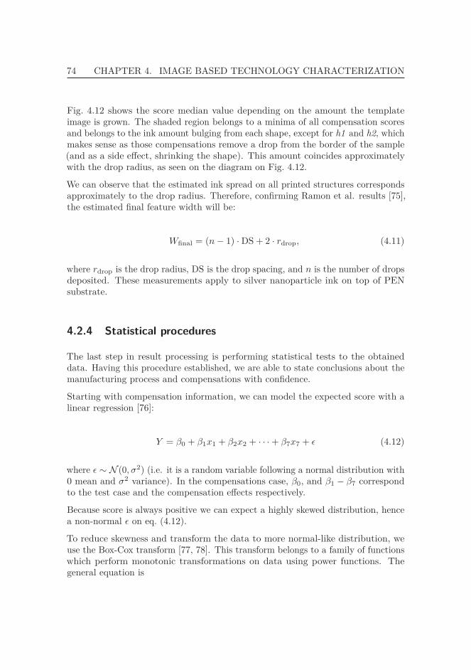
74 CHAPTER 4. IMAGE BASED TECHNOLOGY CHARACTERIZATION
Fig. 4.12 shows the score median value depending on the amount the templateimage is grown. The shaded region belongs to a minima of all compensation scoresand belongs to the ink amount bulging from each shape, except for h1 and h2, whichmakes sense as those compensations remove a drop from the border of the sample(and as a side effect, shrinking the shape). This amount coincides approximatelywith the drop radius, as seen on the diagram on Fig. 4.12.
We can observe that the estimated ink spread on all printed structures correspondsapproximately to the drop radius. Therefore, confirming Ramon et al. results [75],the estimated final feature width will be:
Wfinal = (n − 1) · DS + 2 · rdrop, (4.11)
where rdrop is the drop radius, DS is the drop spacing, and n is the number of dropsdeposited. These measurements apply to silver nanoparticle ink on top of PENsubstrate.
4.2.4 Statistical procedures
The last step in result processing is performing statistical tests to the obtaineddata. Having this procedure established, we are able to state conclusions about themanufacturing process and compensations with confidence.
Starting with compensation information, we can model the expected score with alinear regression [76]:
Y = β0 + β1x1 + β2x2 + · · · + β7x7 + ε (4.12)
where ε ∼ N (0, σ2) (i.e. it is a random variable following a normal distribution with0 mean and σ2 variance). In the compensations case, β0, and β1 − β7 correspondto the test case and the compensation effects respectively.
Because score is always positive we can expect a highly skewed distribution, hencea non-normal ε on eq. (4.12).
To reduce skewness and transform the data to more normal-like distribution, weuse the Box-Cox transform [77, 78]. This transform belongs to a family of functionswhich perform monotonic transformations on data using power functions. Thegeneral equation is

4.2. ANALYSIS 75
Y(λ)
i ={
Y λi −1λ , when λ = 0
ln(Yi), when λ = 0, (4.13)
where λ is extracted from the data. To obtain λ for the score data, we applyMaximum Likelihood Estimator (MLE) methods.
As shown on [79, chap. 14], the log-likelihood of the compensations model can bewritten as
log L = −n
2 log
⎡⎣ n∑
i=1
(Y
(λ)i − (β0 + β1xi)
Y λ
)2⎤⎦ (4.14)
for all our variables of interest. On eq. (4.14), Y is defined as
Y = exp[
1n
n∑i=1
log Yi
](4.15)
Having the likelihood function λ �→ log L, we can find the appropriate λ by findingthe maximum. If desired, an estimated confidence interval for λ can be obtained byintersection with a line at a distance of χ2
α from the maximum.
Fig. 4.13 shows these methods applied to a whole foil. Looking at Fig. 4.13a wecan see that the results are highly positively skewed, therefore we need to applyeq. (4.13) to the data.
The result of applying MLE techniques as in eq. 4.14, and finding the maximumvalue is shown on Fig. 4.13b. Looking at the plot we can assume that λ = 0 for ourdata, therefore the results can be approximated as a log-normal distribution. Notethat λ is not exactly 0, but in order to facilitate future calculations we can use a λvalue from a set of common values from the set λ ∈ {−2, −1, − 1/2, 0, 1/3, 1/2, 1, 2}Table 4.2 contains the measurements of skewness and kurtosis of the transformeddata, and the calculated values approximate to the normal distribution ones.
Once data is transformed and has a normal like distribution we can proceed toestimate means and compare variances. We can observe on Fig. 4.14a that thebox whiskers are approximately the same size, and that the mean and median lieapproximately in the same value. Looking at Fig. 4.14b, which plots the logarithmof the score data quantiles against a theoretical normal distribution, shows a straightline, therefore confirming that the score data is approximately normal.
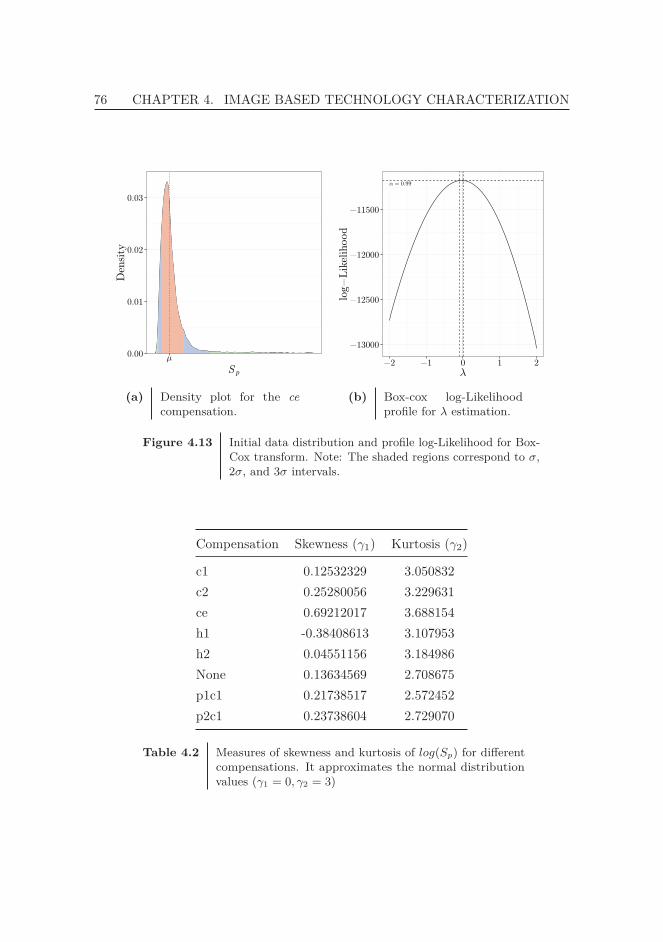
76 CHAPTER 4. IMAGE BASED TECHNOLOGY CHARACTERIZATION
0.00
0.01
0.02
0.03
μ
Sp
Den
sity
(a) Density plot for the cecompensation.
α = 0.99
−13000
−12500
−12000
−11500
−2 −1 0 1 2
λ
log−
Lik
elih
ood
(b) Box-cox log-Likelihoodprofile for λ estimation.
Figure 4.13 Initial data distribution and profile log-Likelihood for Box-Cox transform. Note: The shaded regions correspond to σ,2σ, and 3σ intervals.
Compensation Skewness (γ1) Kurtosis (γ2)
c1 0.12532329 3.050832c2 0.25280056 3.229631ce 0.69212017 3.688154h1 -0.38408613 3.107953h2 0.04551156 3.184986None 0.13634569 2.708675p1c1 0.21738517 2.572452p2c1 0.23738604 2.729070
Table 4.2 Measures of skewness and kurtosis of log(Sp) for differentcompensations. It approximates the normal distributionvalues (γ1 = 0, γ2 = 3)
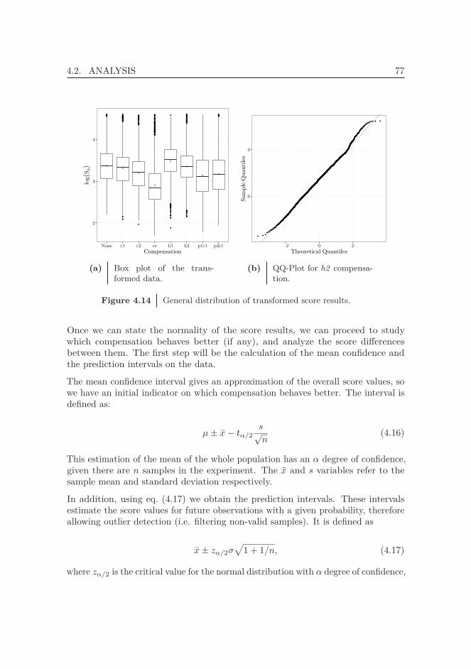
4.2. ANALYSIS 77
●●●●●●●●●●
●
●
●
●●
●
●●
●
●●
●
●
●●
●●
●●●●●●
●●●●
●●
●●
●
●
●●●●
●
●●
●
●
●
●
●
●●
●
●
●●●
●
●●
●●●
●
●
●
●
●●●
●
●
●
●
●
●
●
●●
●●●
●
●●
●
●
●
●
●
●
●
●
●●●
●
●
●
●
●●
●
●
●
●
●
●
●
●
●
●
●
●
●●
●
●
●
●
●●●
●
●
●
●
●●
●●
●●
●
●
●●
●
●
●
●
●
●
●
●●●
●
●
●
●
●
●
●
●
●
●
●●
●
●
●
●
●
●
●●
●
●
●
●
●●
●
●
●
●
●
●
●●●●●
●
●
●
●●●●●
●●
●
●●●
●
●
●
●●
●
●●
●
●
●
●
●
●
●●●
●
●
●●
●
●●
●
●
●
●
●
●
●
●
●
●
●●●
●●
●
●
●●
●
●
●
●
●
●
●●●●●●●●
oo
o
o
o
o
o o
2
3
4
None c1 c2 ce h1 h2 p1c1 p2c1
Compensation
log(S
p)
(a) Box plot of the trans-formed data.
● ●●●●
●●●●●●●●●●●●●
●●●●●●●●●●●●●●●●●●●●●●●●●●●●●●●●●●●●●●●●●●●●●●●●●●●●●●●●●●●●●●●●●●●●●●●●●●●●●●●●●●●●●●●●●●●●●●●●●●●●●●●●●●●●●●●●●●●●●●●●●●●●●●●●●●●●●●●●●●●●●●●●●●●●●●●●●●●●●●●●●●●●●●●●●●●●●●●●●●●●●●●●●●●●●●●●●●●●●●●●●●●●●●●●●●●●●●●●●●●●●●●●●●●●●●●●●●●●●●●●●●●●●●●●●●●●●●●●●●●●●●●●●●●●●●●●●●●●●●●●●●●●●●●●●●●●●●●●●●●●●●●●●●●●●●●●●●●●●●●●●●●●●●●●●●●●●●●●●●●●●●●●●●●●●●●●●●●●●●●●●●●●●●●●●●●●●●●●●●●●●●●●●●●●●●●●●●●●●●●●●●●●●●●●●●●●●●●●●●●●●●●●●●●●●●●●●●●●●●●●●●●●●●●●●●●●●●●●●●●●●●●●●●●●●●●●●●●●●●●●●●●●●●●●●●●●●●●●●●●●●●●●●●●●●●●●●●●●●●●●●●●●●●●●●●●●●●●●●●●●●●●●●●●●●●●●●●●●●●●●●●●●●●●●●●●●●●●●●●●●●●●●●●●●●●●●●●●●●●●●●●●●●●●●●●●●●●●●●●●●●●●●●●●●●●●●●●●●●●●●●●●●●●●●●●●●●●●●●●●●●●●●●●●●●●●●●●●●●●●●●●●●●●●●●●●●●●●●●●●●●●●●●●●●●●●●●●●●●●●●●●●●●●●●●●●●●●●●●●●●●●●●●●●●●●●●●●●●●●●●●●●●●●●●●●●●●●●●●●●●●●●●●●●●●●●●●●●●●●●●●●●●●●●●●●●●●●●●●●●●●●●●●●●●●●●●●●●●●●●●●●●●●●●●●●●●●●●●●●●●●●●●●●●●●●●●●●●●●●●●●●●●●●●●●●●●●●●●●●●●●●●●●●●●●●●●●●●●●●●●●●●●●●●●●●●●●●●●●●●●●●●●●●●●●●●●●●●●●●●●●●●●●●●●●●●●●●●●●●●●●●●●●●●●●●●●●●●●●●●●●●●●●●●●●●●●●●●●●●●●●●●●●●●●●●●●●●●●●●●●●●●●●●●●●●●●●●●●●●●●●●●●●●●●●●●●●●●●●●●●●●●●●●●●●●●●●●●●●●●●●●●●●●●●●●●●●●●●●●●●●●●●●●●●●●●●●●●●●●●●●●●●●●●●●●●●●●●●●●●●●●●●●●●●●●●●●●●●●●●●●●●●●●●●●●●●●●●●●●●●●●●●●●●●●●●●●●●●●●●●●●●●●●●●●●●●●●●●●●●●●●●●●●●●●●●●●●●●●●●●●●●●●●●●●●●●●●●●●●●●●●●●●●●●●●●●●●●●●●●●●●●●●●●●●●●●●●●●●●●●●●●●●●●●●●●●●●●●●●●●●●●●●●●●●●●●●●●●●●●●●●●●●●●●●●●●●●●●●●●●●●●●●●●●●●●●●●●●●●●●●●●●●●●●●●●●●●●●●●●●●●●●●●●●●●●●●●●●●●●●●●●●●●●●●●●●●●●●●●●●●●●●●●●●●●●●●●●●●●●●●●●●●●●●●●●●●●●●●●●●●●●●●●●●●●●●●●●●●●●●●●●●●●●●●●●●●●●●●●●●●●●●●●●●●●●●●●●●●●●●●●●●●●●●●●●●●●●●●●●●●●●●●●●●●●●●●●●●●●●●●●●●●●●●●●●●●●●●●●●●●●●●●●●●●●●●●●●●●●●●●●●●●●●●●●●●●●●●●●●●●●●●●●●●●●●●●●●●●●●●●●●●●●●●●●●●●●●●●●●●●●●●●●●●●●●●●●●●●●●●●●●●●●●●●●●●●●●●●●●●●●●●●●●●●●●●●●●●●●●●●●●●●●●●●●●●●●●●●●●●●●●●●●●●●●●●●●●●●●●●●●●●●●●●●●●●●●●●●●●●●●●●●●●●●●●●●●●●●●●●●●●●●●●●●●●●●●●●●●●●●●●●●●●●●●●●●●●●●●●●●●●●●●●●●●●●●●●●●●●●●●●●●●●●●●●●●●●●●●●●●●●●●●●●●●●●●●●●●●●●●●●●●●●●●●●●●●●●●●●●●●●●●●●●●●●●●●●●●●●●●●●●●●●●●●●●●●●●●●●●●●●●●●●●●●●●●●●●●●●●●●●●●●●●●●●●●●●●●●●●●●●●●●●●●●●●●●●●●●●●●●●●●●●●●●●●●●●●●●●●●●●●●●●●●●●●●●●●●●●●●●●●●●●●●●●●●●●●●●●●●●●●●●●●●●●●●●●●●●●●●●●●●●●●●●●●●●●●●●●●●●●●●●●●●●●●●●●●●●●●●●●●●●●●●●●●●●●●●●●●●●●●●●●●●●●●●●●●●●●●●●●●●●●●●●●●●●●●●●●●●●●●●●●●●●●●●●●●●●●●●●●●●●●●●●●●●●●●●●●●●●●●●●●●●●●●●●●●●●●●●●●●●●●●●●●●●●●●●●●●●●●●●●●●●●●●●●●●●●●●●●●●●●●●●●●●●●●●●●●●●●●●●●●●●●●●●●●●●●●●●●●●●●●●●●●●●●●●●●●●●●●●●●●●●●●●●●●●●●●●●●●●●●●●●●●●●●●●●●●●●●●●●●●●●●●●●●●●●●●●●●●●●●●●●●●●●●●●●●●●●●●●●●●●●●●●●●●●●●●●●●●●●●●●●●●●●●●●●●●●●●●●●●●●●●●●●●●●●●●●●●●●●●●●●●●●●●●●●●●●●●●●●●●●●●●●●●●●●●●●●●●●●●●●●●●●●●●●●●●●●●●●●●●●●●●●●●●●●●●●●●●●●●●●●●●●●●●●●●●●●●●●●●●●●●●●●●●●●●●●●●●●●●●●●●●●●●●●●●●●●●●●●●●●●●●●●●●●●●●●●●●●●●●●●●●●●●●●●●●●●●●●●●●●●●●●●●●●●●●●●●●●●●●●●●●●●●●●●●●●●●●●●●●●●●●●●●●●●●●●●●●●●●●●●●●●●●●●●●●●●●●●●●●●●●●●●●●●●●●●●●●●●●●●●●●●●●●●●●●●●●●●●●●●●●●●●●●●●●●●●●●●●●●●●●●●●●●●●●●●●●●●●●●●●●●●●●●●●●●●●●●●●●●●●●●●●●●●●●●●●●●●●●●●●●●●●●●●●●●●●●●●●●●●●●●●●●●●●●●●●●●●●●●●●●●●●●●●●●●●●●●●●●●●●●●●●●●●●●●●●●●●●●●●●●●●●●●●●●●●●●●●●●●●●●●●●●●●●●●●●●●●●●●●●●●●●●●●●●●●●●●●●●●●●●●●●●●●●●●●●●●●●●●●●●●●●●●●●●●●●●●●●●●●●●●●●●●●●●●●●●●●●●●●●●●●●●●●●●●●●●●●●●●●●●●●●●●●●●●●●●●●●●●●●●●●●●●●●●●●●●●●●●●●●●●●●●●●●●●●●●●●●●●●●●●●●●●●●●●●●●●●●●●●●●●●●●●●●●●●●●●●●●●●●●●●●●●●●●●●●●●●●●●●●●●●●●●●●●●●●●●●●●●●●●●●●●●●●●●●●●●●●●●●●●●●●●●●●●●●●●●●●●●●●●●●●●●●●●●●●●●●●●●●●●●●●●●●●●●●●●●●●●●●●●●●●●●●●●●●●●●●●●●●●●●●●●●●●●●●●●●●●●●●●●●●●●●●●●●●●●●●●●●●●●●●●●●●●●●●●●●●●●●●●●●●●●●●●●●●●●●●●●●●●●●●●●●●●●●●●●●●●●●●●●●●●●●●●●●●●●●●●●●●●●●●●●●●●●●●●●●●
●●●●●● ● ●
3
4
−2 0 2
Theoretical Quantiles
Sam
ple
Quanti
les
(b) QQ-Plot for h2 compensa-tion.
Figure 4.14 General distribution of transformed score results.
Once we can state the normality of the score results, we can proceed to studywhich compensation behaves better (if any), and analyze the score differencesbetween them. The first step will be the calculation of the mean confidence andthe prediction intervals on the data.
The mean confidence interval gives an approximation of the overall score values, sowe have an initial indicator on which compensation behaves better. The interval isdefined as:
μ ± x − tα/2s√n
(4.16)
This estimation of the mean of the whole population has an α degree of confidence,given there are n samples in the experiment. The x and s variables refer to thesample mean and standard deviation respectively.
In addition, using eq. (4.17) we obtain the prediction intervals. These intervalsestimate the score values for future observations with a given probability, thereforeallowing outlier detection (i.e. filtering non-valid samples). It is defined as
x ± zα/2σ√
1 + 1/n, (4.17)
where zα/2 is the critical value for the normal distribution with α degree of confidence,
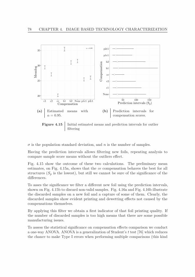
78 CHAPTER 4. IMAGE BASED TECHNOLOGY CHARACTERIZATION
●
●
●
●
●
●
●
●
α = 0.95
20
25
30
35
c1 c2 ce h1 h2 None p1c1 p2c1
Compensation
Mea
nlo
g
(a) Estimated means withα = 0.95.
●
●
●
●
●
●
●
●
None
c1
c2
ce
h1
h2
p1c1
p2c1
50 100 150
Prediction intervals (Sp)C
om
pen
sati
on
(b) Prediction intervals forcompensation scores.
Figure 4.15 Initial estimated means and prediction intervals for outlierfiltering
σ is the population standard deviation, and n is the number of samples.
Having the prediction intervals allows filtering new foils, repeating analysis tocompare sample score means without the outliers effect.
Fig. 4.15 show the outcome of these two calculations. The preliminary meanestimates, on Fig. 4.15a, shows that the ce compensation behaves the best for allstructures (Sp is the lowest), but still we cannot be sure of the significance of thedifferences.
To asses the significance we filter a different new foil using the prediction intervals,shown on Fig. 4.15b to discard non-valid samples. Fig. 4.16a and Fig. 4.16b illustratethe discarded samples on a new foil and a capture of some of them. Clearly, thediscarded samples show evident printing and dewetting effects not caused by thecompensations themselves.
By applying this filter we obtain a first indicator of that foil printing quality. Ifthe number of discarded samples is too high means that there are some possiblemanufacturing issues.
To assess the statistical significance on compensation effects comparison we conducta one-way ANOVA. ANOVA is a generalization of Student’s t test [76] which reducesthe chance to make Type I errors when performing multiple comparisons (this kind
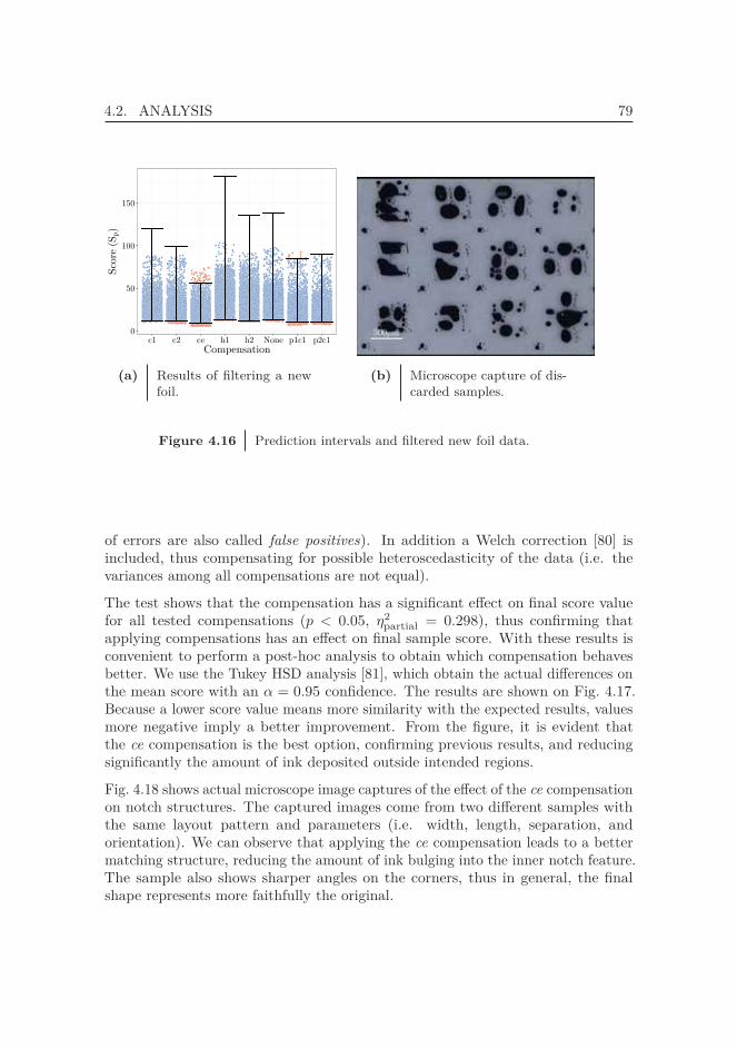
4.2. ANALYSIS 79
0
50
100
150
c1 c2 ce h1 h2 None p1c1 p2c1
Compensation
Sco
re (
Sp)
(a) Results of filtering a newfoil.
(b) Microscope capture of dis-carded samples.
Figure 4.16 Prediction intervals and filtered new foil data.
of errors are also called false positives). In addition a Welch correction [80] isincluded, thus compensating for possible heteroscedasticity of the data (i.e. thevariances among all compensations are not equal).
The test shows that the compensation has a significant effect on final score valuefor all tested compensations (p < 0.05, η2
partial = 0.298), thus confirming thatapplying compensations has an effect on final sample score. With these results isconvenient to perform a post-hoc analysis to obtain which compensation behavesbetter. We use the Tukey HSD analysis [81], which obtain the actual differences onthe mean score with an α = 0.95 confidence. The results are shown on Fig. 4.17.Because a lower score value means more similarity with the expected results, valuesmore negative imply a better improvement. From the figure, it is evident thatthe ce compensation is the best option, confirming previous results, and reducingsignificantly the amount of ink deposited outside intended regions.
Fig. 4.18 shows actual microscope image captures of the effect of the ce compensationon notch structures. The captured images come from two different samples withthe same layout pattern and parameters (i.e. width, length, separation, andorientation). We can observe that applying the ce compensation leads to a bettermatching structure, reducing the amount of ink bulging into the inner notch feature.The sample also shows sharper angles on the corners, thus in general, the finalshape represents more faithfully the original.
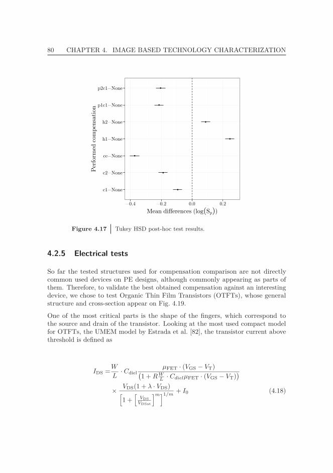
80 CHAPTER 4. IMAGE BASED TECHNOLOGY CHARACTERIZATION
●
●
●
●
●
●
●
c1−None
c2−None
ce−None
h1−None
h2−None
p1c1−None
p2c1−None
−0.4 −0.2 0.0 0.2
Mean differences (log(Sp))
Per
form
ed c
om
pen
sati
on
Figure 4.17 Tukey HSD post-hoc test results.
4.2.5 Electrical tests
So far the tested structures used for compensation comparison are not directlycommon used devices on PE designs, although commonly appearing as parts ofthem. Therefore, to validate the best obtained compensation against an interestingdevice, we chose to test Organic Thin Film Transistors (OTFTs), whose generalstructure and cross-section appear on Fig. 4.19.
One of the most critical parts is the shape of the fingers, which correspond tothe source and drain of the transistor. Looking at the most used compact modelfor OTFTs, the UMEM model by Estrada et al. [82], the transistor current abovethreshold is defined as
IDS =W
L· Cdiel
μFET · (VGS − VT)(1 + R W
L · CdielμFET · (VGS − VT))
× VDS(1 + λ · VDS)[1 +
[VDS
VDSat
]m]1/m+ I0 (4.18)

4.2. ANALYSIS 81
(a) none compensation. (b) ce compensation.
(c) Ideal expected result(from design).
Figure 4.18 Comparison of the same structure with different compen-sations.
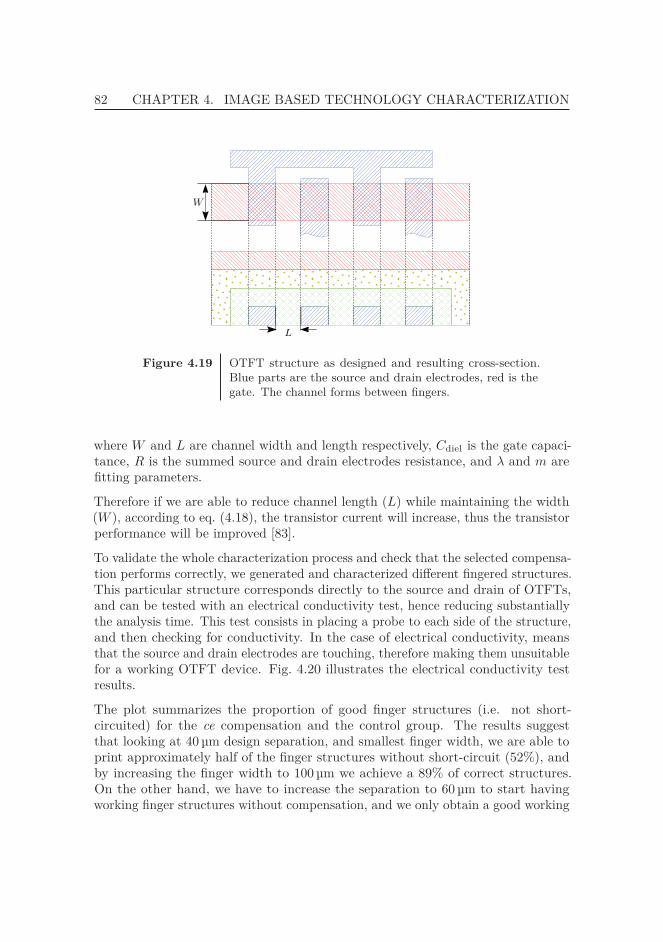
82 CHAPTER 4. IMAGE BASED TECHNOLOGY CHARACTERIZATION
Figure 4.19 OTFT structure as designed and resulting cross-section.Blue parts are the source and drain electrodes, red is thegate. The channel forms between fingers.
where W and L are channel width and length respectively, Cdiel is the gate capaci-tance, R is the summed source and drain electrodes resistance, and λ and m arefitting parameters.
Therefore if we are able to reduce channel length (L) while maintaining the width(W ), according to eq. (4.18), the transistor current will increase, thus the transistorperformance will be improved [83].
To validate the whole characterization process and check that the selected compensa-tion performs correctly, we generated and characterized different fingered structures.This particular structure corresponds directly to the source and drain of OTFTs,and can be tested with an electrical conductivity test, hence reducing substantiallythe analysis time. This test consists in placing a probe to each side of the structure,and then checking for conductivity. In the case of electrical conductivity, meansthat the source and drain electrodes are touching, therefore making them unsuitablefor a working OTFT device. Fig. 4.20 illustrates the electrical conductivity testresults.
The plot summarizes the proportion of good finger structures (i.e. not short-circuited) for the ce compensation and the control group. The results suggestthat looking at 40 μm design separation, and smallest finger width, we are able toprint approximately half of the finger structures without short-circuit (52%), andby increasing the finger width to 100 μm we achieve a 89% of correct structures.On the other hand, we have to increase the separation to 60 μm to start havingworking finger structures without compensation, and we only obtain a good working
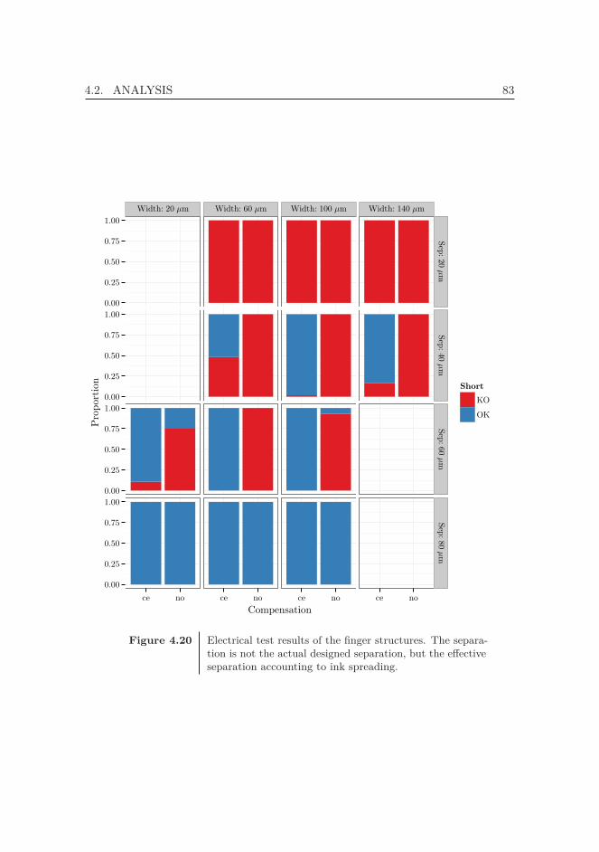
4.2. ANALYSIS 83
Width: 20 μm Width: 60 μm Width: 100 μm Width: 140 μm
0.00
0.25
0.50
0.75
1.00
0.00
0.25
0.50
0.75
1.00
0.00
0.25
0.50
0.75
1.00
0.00
0.25
0.50
0.75
1.00
Sep
: 20 μ
mSep
: 40 μ
mSep
: 60 μ
mSep
: 80 μ
m
ce no ce no ce no ce no
Compensation
Pro
port
ion
Short
KO
OK
Figure 4.20 Electrical test results of the finger structures. The separa-tion is not the actual designed separation, but the effectiveseparation accounting to ink spreading.

84 CHAPTER 4. IMAGE BASED TECHNOLOGY CHARACTERIZATION
40 μm sep. 60 μm sep.
20 μm width ce —† 0.893 ± 0.061no —† 0.250 ± 0.146
60 μm width ce 0.519 ± 0.130 1.000 ± 0.017no 0.000 ± 0.079 0.000 ± 0.077
100 μm width ce 0.981 ± 0.025 1.000 ± 0.016no 0.000 ± 0.084 0.070 ± 0.123
†This samples were not generated because the finger widthis too low, so the compensation cannot be applied.
Table 4.3 Approximated α = 0.95 confidence intervals for proportionof working fingers.
proportion if we double the minimal separation, resulting to 80 μm.
The electrical results summarized on 4.20 can be modelled with a binomial distribu-tion because the outcomes are independent success/failure experiments (i.e. there isa short-circuit or not). Therefore, approximating the distribution error as a normaldistribution [84], we can calculate the confidence intervals as:
p ± zα/2√
p(1 − p)/n, (4.19)
where p is the proportion of successes, n is the number of samples, and zα/2 is thenormal percentile for an α confidence. This interval approximation does not behavecorrectly when p is close to 0 or 1. To compensate this effect, Agresti et al. [85],and Bonett et al. [86] propose some adjustments. Then, the interval is defined as:
p ±√
1n
p(1 − p) (4.20)
where n = n + z2α/2, p = 1
n
(X + 1
2 z2α/2
), and X is the number of successes.
Table 4.3 has the calculated α = 0.95 confidence intervals for some interesting fingerwidths and separations. We can observe that even with a 20 μm separation theyield improves around 50%, and by making the fingers 120 μm wide, the number ofworking structures raise to 98%.
As an example of the improvement achieved with the compensation, Fig. 4.21 shows
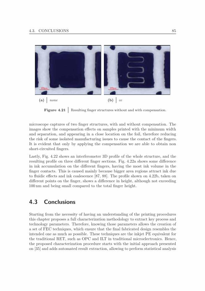
4.3. CONCLUSIONS 85
(a) none (b) ce
Figure 4.21 Resulting finger structures without and with compensation.
microscope captures of two finger structures, with and without compensation. Theimages show the compensation effects on samples printed with the minimum widthand separation, and appearing in a close location on the foil, therefore reducingthe risk of some isolated manufacturing issues to cause the contact of the fingers.It is evident that only by applying the compensation we are able to obtain nonshort-circuited fingers.
Lastly, Fig. 4.22 shows an interferometer 3D profile of the whole structure, and theresulting profile on three different finger sections. Fig. 4.22a shows some differencein ink accumulation on the different fingers, having the most ink volume in thefinger contacts. This is caused mainly because bigger area regions attract ink dueto fluidic effects and ink coalescence [87, 88]. The profile shown on 4.22b, taken ondifferent points on the finger, shows a difference in height, although not exceeding100 nm and being small compared to the total finger height.
4.3 Conclusions
Starting from the necessity of having an understanding of the printing proceduresthis chapter proposes a full characterization methodology to extract key process andtechnology parameters. Therefore, knowing those parameters allows the creation ofa set of FEC techniques, which ensure that the final fabricated design resembles theintended one as much as possible. These techniques are the inkjet PE equivalent forthe traditional RET, such as OPC and ILT in traditional microelectronics. Hence,the proposed characterization procedure starts with the initial approach presentedon [35] and adds automated result extraction, allowing to perform statistical analysis
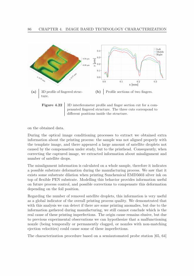
86 CHAPTER 4. IMAGE BASED TECHNOLOGY CHARACTERIZATION
(a) 3D profile of fingered struc-ture.
0.0
0.1
0.2
0.3
0.4
0.0 0.1 0.2 0.3
x [mm]
y [μ
m]
LeftMiddleRight
(b) Profile sections of two fingers.
Figure 4.22 3D interferometer profile and finger section cut for a com-pensated fingered structure. The three cuts correspond todifferent positions inside the structure.
on the obtained data.
During the optical image conditioning processes to extract we obtained extrainformation about the printing process: the sample was not aligned properly withthe template image, and there appeared a large amount of satellite droplets notcaused by the compensation under study, but to the printhead. Consequently, whencorrecting the captured image, we extracted information about misalignment andnumber of satellite drops.
The misalignment information is calculated on a whole sample, therefore it indicatesa possible substrate deformation during the manufacturing process. We saw that itexists some substrate dilation when printing Sunchemical EMD5603 silver ink ontop of flexible PEN substrate. Modelling this behavior provides information usefulon future process control, and possible corrections to compensate this deformationdepending on the foil position.
Regarding the number of removed satellite droplets, this information is very usefulas a global indicator of the overall printing process quality. We demonstrated thatwith this analysis we can detect if there are some printing anomalies, but due to theinformation gathered during manufacturing, we still cannot conclude which is thereal cause of these printing imperfections. The origin cause remains elusive, but dueto previous experimental observations we can hypothesize that a malfunctioningnozzle (being temporally or permanently clogged, or nozzles with non-matchingejection velocities) could cause some of these imperfections.
The characterization procedure based on a semiautomated probe station [65, 64]

4.3. CONCLUSIONS 87
allowed the mass-characterization of more than half a million printed samples withoutrequiring high manual intervention, therefore obtaining statistical significant results.Specifically for the used silver nanoparticles ink on top of flexible PEN substrateusing industrial D-class DPN 10 pL printheads, the results have been consistentalong different foils printed on different runs spanning several days. Furthermore,the best compensation obtained have been successfully verified using transistor fingerstructures performing electrical continuity tests. The results show an outstandingimprovement on shape morphologies, obtaining detailed fingered structures withoutelectrical short circuits. This is of relevant importance in the fabrication of devicessuch as capacitors or transistors where interdigitated structures are used, becausethe printed shape is critical for device performance, and the whole process stability.The proposed compensation improves shape morphology allowing scaling down,thus improving resolution and process yield.

AutomaticCompensations: The
Layout2Bitmap tape-outframework 5
After characterizing ink behaviour and extracting which are the appropriate com-pensation strategies, rules, and patterns for the specific process, we need to movethem into the actual automatic tape-out processes to obtain directly printabledesigns.
Therefore, for our technology setup, based in a fully inkjet printing process using aDimatix printer, we need some framework which converts typical CAD formats toa set of bitmap files, which will define each drop final position.
5.1 Layout2Bitmap
The Layout2Bitmap, from now on L2B, is the responsible of reading the design andgenerating a set of bitmaps for each printing layer. For each layer, or layer region,it will apply the needed compensations according to the technology description.
5.1.1 Tool description
L2B is the tool which performs the conversions from final layout designs to directlyprintable bitmap files. Initially the conversion was just devoted to the discretization
89
90 CHAPTER 5. AUTOMATIC COMPENSATIONS
of the design to a bitmap having the printer resolution, but following this thesisevolution we implemented several different options and optimizations. CurrentlyL2B incorporates most of the compensation results in terms of patterns and rulesobtained from the previous chapter results.
Therefore, being able to use the L2B tool since the start of the project and evolvingit according to characterization results, allowed its use in the characterizationprocedures. This helped both in bug solving, and in speeding the tape-out forexperiment generation.
The procedures implemented by L2B to perform these automatic compensationsand conversions are succinctly: Loading the design, reading the appropriate compen-sations, performing all the optimizations, and generating the final set of printablefiles. All of these steps are described thoroughly along the following sections.
5.1.2 Design loading
In order to export the design, it is necessary a format which is widely supportedacross microelectronics CAD tools, while allowing some customization or extensibil-ity, thus enabling adding custom technology information.
After the evaluation of several alternatives, we chose to use the GDS streamformat [89]. This format originally developed by Calma in 1970, was used forcontrolling integrated circuit photomask plotting. From then, it became a de factoindustry standard for data exchange at layout level. It is used often as the last stepin the design physical cycle, acting as a foundry interface format.
There is a newer alternative, the successor of the GDS format Open ArtworkSystem Interchange Standard (OASIS), which is maintained by SEMI internationalstandards association. Although it presents some improvements over GDS, suchas smaller file size and new primitive types, the format specification is private andthere are more tools supporting GDS rather than OASIS.
GDS File format
The GDS stream format is a binary format which describes a library (in our case adesign), which consists in several structures (i.e. cells). Each structure containsseveral primitive elements, or references to other cells, allowing hierarchical designs.The file also contains some metadata, such as creation and modification times, forthe library and the structures.
The available element types supported by this specification are:
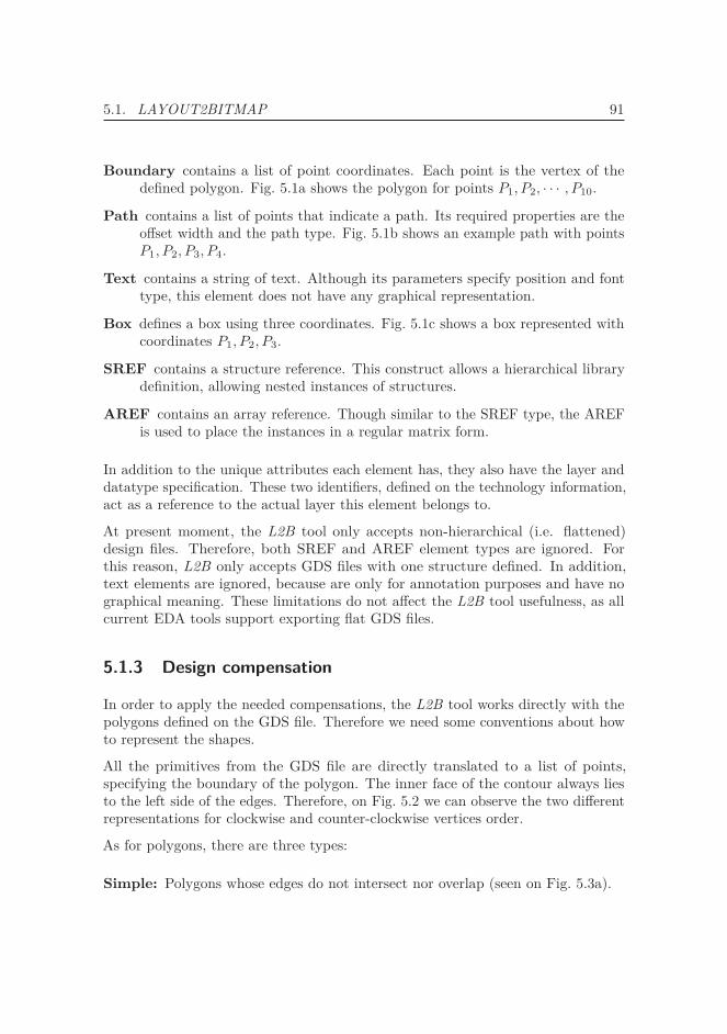
5.1. LAYOUT2BITMAP 91
Boundary contains a list of point coordinates. Each point is the vertex of thedefined polygon. Fig. 5.1a shows the polygon for points P1, P2, · · · , P10.
Path contains a list of points that indicate a path. Its required properties are theoffset width and the path type. Fig. 5.1b shows an example path with pointsP1, P2, P3, P4.
Text contains a string of text. Although its parameters specify position and fonttype, this element does not have any graphical representation.
Box defines a box using three coordinates. Fig. 5.1c shows a box represented withcoordinates P1, P2, P3.
SREF contains a structure reference. This construct allows a hierarchical librarydefinition, allowing nested instances of structures.
AREF contains an array reference. Though similar to the SREF type, the AREFis used to place the instances in a regular matrix form.
In addition to the unique attributes each element has, they also have the layer anddatatype specification. These two identifiers, defined on the technology information,act as a reference to the actual layer this element belongs to.
At present moment, the L2B tool only accepts non-hierarchical (i.e. flattened)design files. Therefore, both SREF and AREF element types are ignored. Forthis reason, L2B only accepts GDS files with one structure defined. In addition,text elements are ignored, because are only for annotation purposes and have nographical meaning. These limitations do not affect the L2B tool usefulness, as allcurrent EDA tools support exporting flat GDS files.
5.1.3 Design compensation
In order to apply the needed compensations, the L2B tool works directly with thepolygons defined on the GDS file. Therefore we need some conventions about howto represent the shapes.
All the primitives from the GDS file are directly translated to a list of points,specifying the boundary of the polygon. The inner face of the contour always liesto the left side of the edges. Therefore, on Fig. 5.2 we can observe the two differentrepresentations for clockwise and counter-clockwise vertices order.
As for polygons, there are three types:
Simple: Polygons whose edges do not intersect nor overlap (seen on Fig. 5.3a).
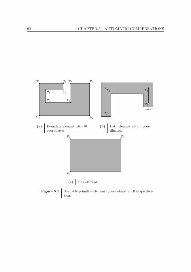
92 CHAPTER 5. AUTOMATIC COMPENSATIONS
(a) Boundary element with 10coordinates.
width
(b) Path element with 4 coor-dinates.
(c) Box element.
Figure 5.1 Available primitive element types defined in GDS specifica-tion.
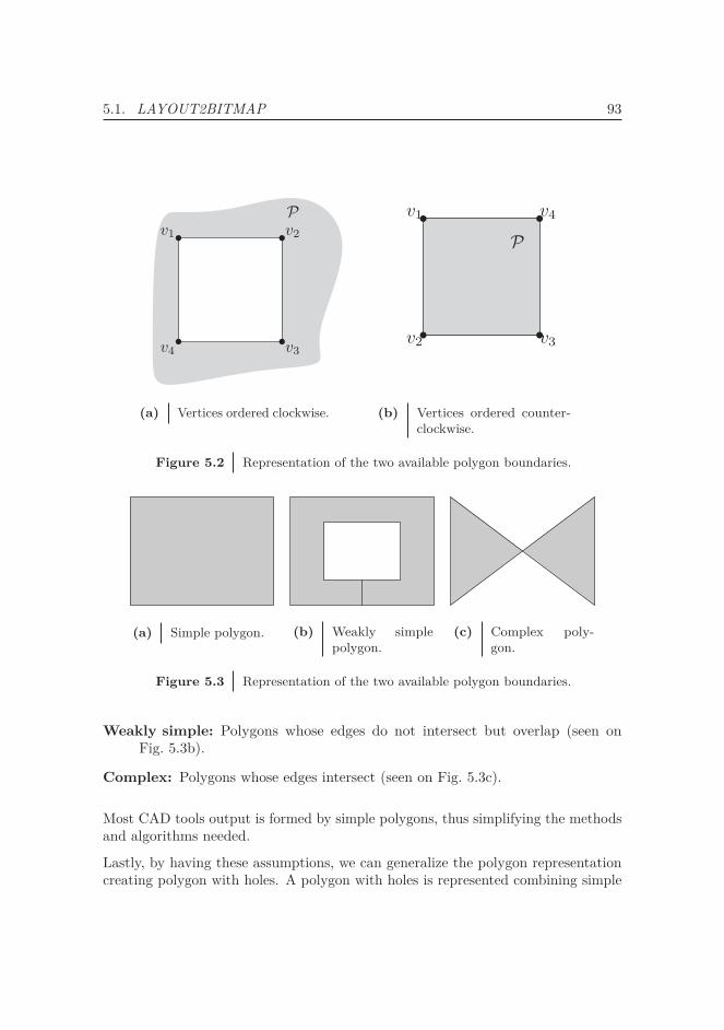
5.1. LAYOUT2BITMAP 93
Pv1 v2
v3v4
(a) Vertices ordered clockwise.
Pv1
v2 v3
v4
(b) Vertices ordered counter-clockwise.
Figure 5.2 Representation of the two available polygon boundaries.
(a) Simple polygon. (b) Weakly simplepolygon.
(c) Complex poly-gon.
Figure 5.3 Representation of the two available polygon boundaries.
Weakly simple: Polygons whose edges do not intersect but overlap (seen onFig. 5.3b).
Complex: Polygons whose edges intersect (seen on Fig. 5.3c).
Most CAD tools output is formed by simple polygons, thus simplifying the methodsand algorithms needed.
Lastly, by having these assumptions, we can generalize the polygon representationcreating polygon with holes. A polygon with holes is represented combining simple
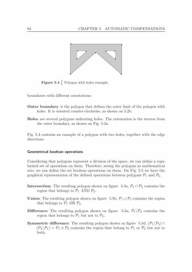
94 CHAPTER 5. AUTOMATIC COMPENSATIONS
Figure 5.4 Polygon with holes example.
boundaries with different orientations:
Outer boundary is the polygon that defines the outer limit of the polygon withholes. It is oriented counter-clockwise, as shown on 5.2b.
Holes are several polygons indicating holes. The orientation is the inverse fromthe outer boundary, as shown on Fig. 5.2a.
Fig. 5.4 contains an example of a polygon with two holes, together with the edgedirections.
Geometrical boolean operations
Considering that polygons represent a division of the space, we can define a regu-larized set of operations on them. Therefore, seeing the polygons as mathematicalsets, we can define the set boolean operations on them. On Fig. 5.5 we have thegraphical representation of the defined operations between polygons P1 and P2.
Intersection: The resulting polygon shown on figure 5.5a, P1 ∩ P2 contains theregion that belongs to P1 AND P2.
Union: The resulting polygon shown on figure 5.5b, P1 ∪ P2 contains the regionthat belongs to P1 OR P2.
Difference: The resulting polygon shown on figure 5.5a, P1\P2 contains theregion that belongs to P1 but not to P2.
Symmetric difference: The resulting polygon shown on figure 5.5d, (P1\P2) ∩(P2\P1) = P1 ⊕ P2 contains the region that belong to P1 or P2 but not toboth.
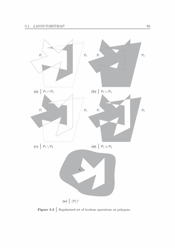
5.1. LAYOUT2BITMAP 95
P1 P2
(a) P1 ∩ P2
P1 P2
(b) P1 ∪ P2
P1 P2
(c) P1 \ P2
P1 P2
(d) P1 ⊕ P2
P1
(e) (P1)c
Figure 5.5 Regularized set of boolean operations on polygons.
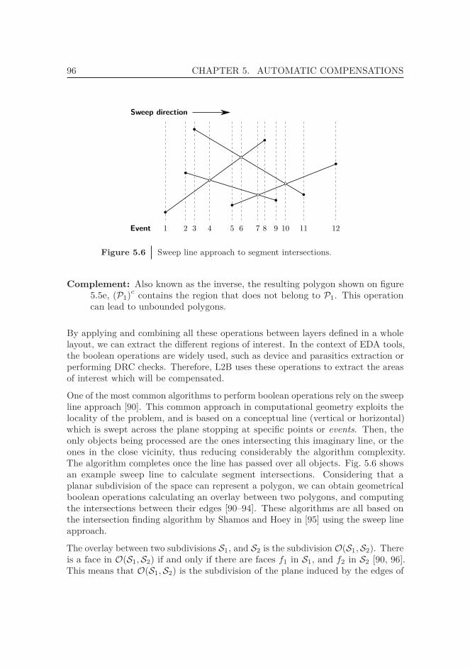
96 CHAPTER 5. AUTOMATIC COMPENSATIONS
Event 1 2 3 4 5 6 7 8 9 10 11 12
Sweep direction
Figure 5.6 Sweep line approach to segment intersections.
Complement: Also known as the inverse, the resulting polygon shown on figure5.5e, (P1)c contains the region that does not belong to P1. This operationcan lead to unbounded polygons.
By applying and combining all these operations between layers defined in a wholelayout, we can extract the different regions of interest. In the context of EDA tools,the boolean operations are widely used, such as device and parasitics extraction orperforming DRC checks. Therefore, L2B uses these operations to extract the areasof interest which will be compensated.
One of the most common algorithms to perform boolean operations rely on the sweepline approach [90]. This common approach in computational geometry exploits thelocality of the problem, and is based on a conceptual line (vertical or horizontal)which is swept across the plane stopping at specific points or events. Then, theonly objects being processed are the ones intersecting this imaginary line, or theones in the close vicinity, thus reducing considerably the algorithm complexity.The algorithm completes once the line has passed over all objects. Fig. 5.6 showsan example sweep line to calculate segment intersections. Considering that aplanar subdivision of the space can represent a polygon, we can obtain geometricalboolean operations calculating an overlay between two polygons, and computingthe intersections between their edges [90–94]. These algorithms are all based onthe intersection finding algorithm by Shamos and Hoey in [95] using the sweep lineapproach.
The overlay between two subdivisions S1, and S2 is the subdivision O(S1, S2). Thereis a face in O(S1, S2) if and only if there are faces f1 in S1, and f2 in S2 [90, 96].This means that O(S1, S2) is the subdivision of the plane induced by the edges of
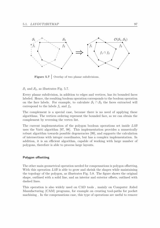
5.1. LAYOUT2BITMAP 97
Figure 5.7 Overlay of two planar subdivisions.
S1 and S2, as illustrates Fig. 5.7.
Every planar subdivision, in addition to edges and vertices, has its bounded faceslabeled. Hence, the resulting boolean operation corresponds to the boolean operationon the face labels. For example, to calculate S1 ∩ S2 the faces extracted willcorrespond to the labels f1 and f2.
The complement is a special case, because there is no need of applying thesealgorithms. The vertices ordering represent the bounded face, so we can obtain thecomplement by reversing the vertex list.
The current implementation of the polygon boolean operations set inside L2Buses the Vatti algorithm [97, 98]. This implementation provides a numericallyrobust algorithm towards possible degeneracies [99], and supports the calculationof intersections with integer coordinates, but has a complex implementation. Inaddition, it is an efficient algorithm, capable of working with large number ofpolygons, therefore is able to process large layouts.
Polygon offsetting
The other main geometrical operation needed for compensations is polygon offsetting.With this operation L2B is able to grow and shrink the shapes while maintainingthe topology of the polygon, as illustrates Fig. 5.8. The figure shows the originalshape, outlined with a solid line, and an interior and exterior offsets, outlined withdashed lines.
This operation is also widely used on CAD tools , mainly on Computer AidedManufacturing (CAM) programs, for example on creating tool-paths for pocketmachining . In the compensations case, this type of operations are useful to remove
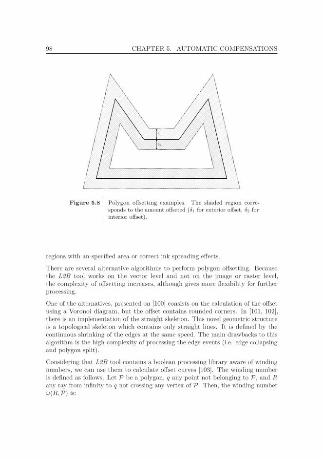
98 CHAPTER 5. AUTOMATIC COMPENSATIONS
Figure 5.8 Polygon offsetting examples. The shaded region corre-sponds to the amount offseted (δ1 for exterior offset, δ2 forinterior offset).
regions with an specified area or correct ink spreading effects.
There are several alternative algorithms to perform polygon offsetting. Becausethe L2B tool works on the vector level and not on the image or raster level,the complexity of offsetting increases, although gives more flexibility for furtherprocessing.
One of the alternatives, presented on [100] consists on the calculation of the offsetusing a Voronoi diagram, but the offset contains rounded corners. In [101, 102],there is an implementation of the straight skeleton. This novel geometric structureis a topological skeleton which contains only straight lines. It is defined by thecontinuous shrinking of the edges at the same speed. The main drawbacks to thisalgorithm is the high complexity of processing the edge events (i.e. edge collapsingand polygon split).
Considering that L2B tool contains a boolean processing library aware of windingnumbers, we can use them to calculate offset curves [103]. The winding numberis defined as follows. Let P be a polygon, q any point not belonging to P, and Rany ray from infinity to q not crossing any vertex of P. Then, the winding numberω(R, P) is:
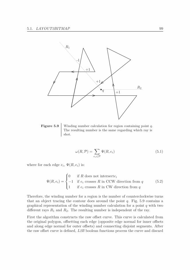
5.1. LAYOUT2BITMAP 99
q+1
-1
+1
+1
R1
R2
Figure 5.9 Winding number calculation for region containing point q.The resulting number is the same regarding which ray isshot.
ω(R, P) =∑
ei∈PΨ(R, ei) (5.1)
where for each edge ei, Ψ(R, ei) is:
Ψ(R, ei) =
⎧⎪⎨⎪⎩
0 if R does not intersectei
−1 if ei crosses R in CCW direction from q
1 if ei crosses R in CW direction from q
(5.2)
Therefore, the winding number for a region is the number of counterclockwise turnsthat an object tracing the contour does around the point q. Fig. 5.9 contains agraphical representation of the winding number calculation for a point q with twodifferent rays R1 and R2. The resulting number is independent of the ray.
First the algorithm constructs the raw offset curve. This curve is calculated fromthe original polygon, offsetting each edge (opposite edge normal for inner offsetsand along edge normal for outer offsets) and connecting disjoint segments. Afterthe raw offset curve is defined, L2B boolean functions process the curve and discard
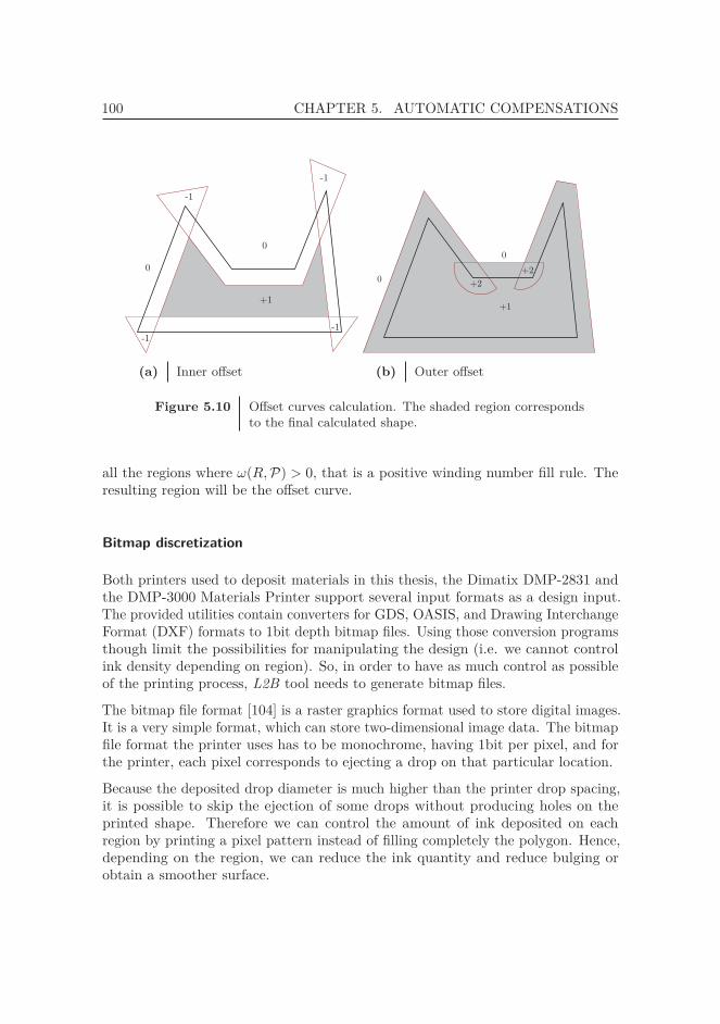
100 CHAPTER 5. AUTOMATIC COMPENSATIONS
-1
-1
0
-1
-1
+1
0
(a) Inner offset
0
+1
0
+2
+2
(b) Outer offset
Figure 5.10 Offset curves calculation. The shaded region correspondsto the final calculated shape.
all the regions where ω(R, P) > 0, that is a positive winding number fill rule. Theresulting region will be the offset curve.
Bitmap discretization
Both printers used to deposit materials in this thesis, the Dimatix DMP-2831 andthe DMP-3000 Materials Printer support several input formats as a design input.The provided utilities contain converters for GDS, OASIS, and Drawing InterchangeFormat (DXF) formats to 1bit depth bitmap files. Using those conversion programsthough limit the possibilities for manipulating the design (i.e. we cannot controlink density depending on region). So, in order to have as much control as possibleof the printing process, L2B tool needs to generate bitmap files.
The bitmap file format [104] is a raster graphics format used to store digital images.It is a very simple format, which can store two-dimensional image data. The bitmapfile format the printer uses has to be monochrome, having 1bit per pixel, and forthe printer, each pixel corresponds to ejecting a drop on that particular location.
Because the deposited drop diameter is much higher than the printer drop spacing,it is possible to skip the ejection of some drops without producing holes on theprinted shape. Therefore we can control the amount of ink deposited on eachregion by printing a pixel pattern instead of filling completely the polygon. Hence,depending on the region, we can reduce the ink quantity and reduce bulging orobtain a smoother surface.
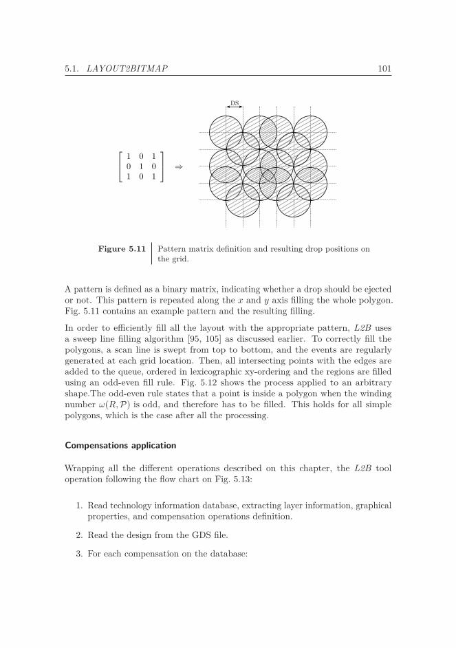
5.1. LAYOUT2BITMAP 101
DS
Figure 5.11 Pattern matrix definition and resulting drop positions onthe grid.
A pattern is defined as a binary matrix, indicating whether a drop should be ejectedor not. This pattern is repeated along the x and y axis filling the whole polygon.Fig. 5.11 contains an example pattern and the resulting filling.
In order to efficiently fill all the layout with the appropriate pattern, L2B usesa sweep line filling algorithm [95, 105] as discussed earlier. To correctly fill thepolygons, a scan line is swept from top to bottom, and the events are regularlygenerated at each grid location. Then, all intersecting points with the edges areadded to the queue, ordered in lexicographic xy-ordering and the regions are filledusing an odd-even fill rule. Fig. 5.12 shows the process applied to an arbitraryshape.The odd-even rule states that a point is inside a polygon when the windingnumber ω(R, P) is odd, and therefore has to be filled. This holds for all simplepolygons, which is the case after all the processing.
Compensations application
Wrapping all the different operations described on this chapter, the L2B tooloperation following the flow chart on Fig. 5.13:
1. Read technology information database, extracting layer information, graphicalproperties, and compensation operations definition.
2. Read the design from the GDS file.
3. For each compensation on the database:
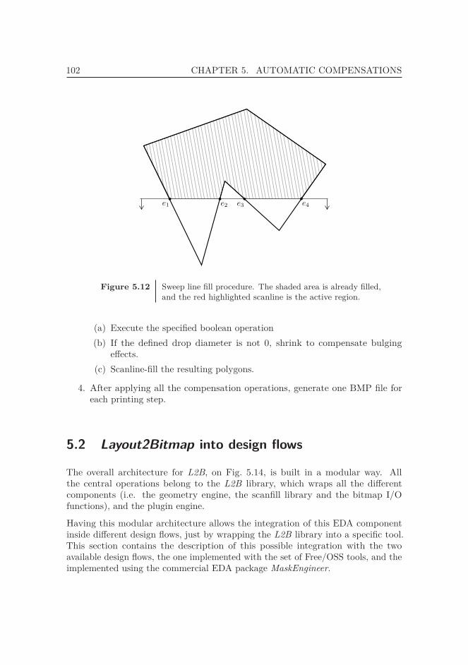
102 CHAPTER 5. AUTOMATIC COMPENSATIONS
Figure 5.12 Sweep line fill procedure. The shaded area is already filled,and the red highlighted scanline is the active region.
(a) Execute the specified boolean operation(b) If the defined drop diameter is not 0, shrink to compensate bulging
effects.(c) Scanline-fill the resulting polygons.
4. After applying all the compensation operations, generate one BMP file foreach printing step.
5.2 Layout2Bitmap into design flows
The overall architecture for L2B, on Fig. 5.14, is built in a modular way. Allthe central operations belong to the L2B library, which wraps all the differentcomponents (i.e. the geometry engine, the scanfill library and the bitmap I/Ofunctions), and the plugin engine.
Having this modular architecture allows the integration of this EDA componentinside different design flows, just by wrapping the L2B library into a specific tool.This section contains the description of this possible integration with the twoavailable design flows, the one implemented with the set of Free/OSS tools, and theimplemented using the commercial EDA package MaskEngineer.
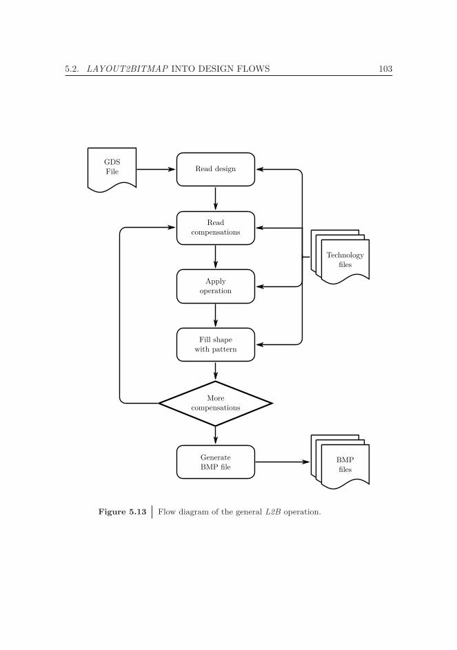
5.2. LAYOUT2BITMAP INTO DESIGN FLOWS 103
Technologyles
Morecompensations
Fill shapewith pattern
Applyoperation
Read compensations
Read designGDSFile
GenerateBMP le
BMPles
Figure 5.13 Flow diagram of the general L2B operation.
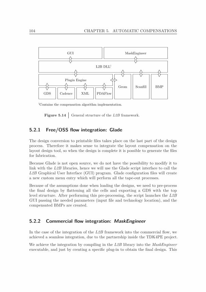
104 CHAPTER 5. AUTOMATIC COMPENSATIONS
†Contains the compensation algorithm implementation.
GUI MaskEngineer
L2B DLL†
Geom Scan ll BMP
GDS Cadence XML PDAFlow
Plugin Engine
Figure 5.14 General structure of the L2B framework.
5.2.1 Free/OSS flow integration: Glade
The design conversion to printable files takes place on the last part of the designprocess. Therefore it makes sense to integrate the layout compensation on thelayout design tool, so when the design is complete it is possible to generate the filesfor fabrication.
Because Glade is not open source, we do not have the possibility to modify it tolink with the L2B libraries, hence we will use the Glade script interface to call theL2B Graphical User Interface (GUI) program. Glade configuration files will createa new custom menu entry which will perform all the tape-out processes.
Because of the assumptions done when loading the designs, we need to pre-processthe final design by flattening all the cells and exporting a GDS with the toplevel structure. After performing this pre-processing, the script launches the L2BGUI passing the needed parameters (input file and technology location), and thecompensated BMPs are created.
5.2.2 Commercial flow integration: MaskEngineer
In the case of the integration of the L2B framework into the commercial flow, weachieved a seamless integration, due to the partnership inside the TDK4PE project.
We achieve the integration by compiling in the L2B library into the MaskEngineerexecutable, and just by creating a specific plug-in to obtain the final design. This
5.3. RESULTS AND CONCLUSIONS 105
integration did not require any modification of the core functionality except for theplug-in. MaskEngineer supports reading the technology information from the sameXML database as L2B, thus not requiring any change.
Because compensations are process dependent, the actual calls to the L2B functionsappear on the design kit creation. According to PDAFlow manual [106, 59], thefoundry definition file contains the function export(string file) which creates thefinal mask designs for the design. In our case, instead of masks, this function createsthe set of BMP files. Listing 5.1 contains the full commented code.
function export(string file) {// Call the process() function for each layerstring all_output = process_design2output("all_output");
// Call the export and compensation functions of L2Bmask::exportToBMP(all_output, file);return 1;
}
// And then, on the final top-level designpdk::pdkExport("directory/to/export/to",
"Processing");
Listing 5.1 Full listing of the export function inside the design kitdefinition for PDAFlow design kits, and its usage.
5.3 Results and conclusions
L2B provides an extensible framework for implementing automated compensations.Being able to characterize and extract the needed compensation operations for agiven technology process (see chapter 4), provides the final element needed to closethe gap between designers and technology developers.
The framework architecture allows an easy integration into different design flowscovered by different tools. As a demonstration, L2B has been integrated into twodifferent design flows, one implemented using Free/OSS tools, and the other usinga commercial package.
In addition L2B can perform different compensations, due to the full set of compu-tational geometry algorithms it implements. Therefore, once we can extract thenecessary operations for a specific technology process, they can be easily imple-mented.

106 CHAPTER 5. AUTOMATIC COMPENSATIONS
As the result of its plug-in engine, the L2B framework can be extended to other inputfile formats without modifying the core functionality. This has been demonstrated bywriting a plug-in capable of reading the information directly from the MaskEngineermask format.
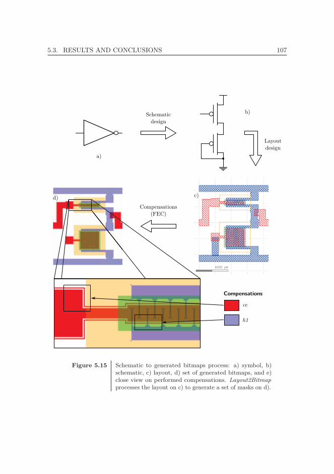
5.3. RESULTS AND CONCLUSIONS 107
a)
b)
d) c)
e)
Schematicdesign
Layoutdesign
Compensations(FEC)
ce
h1
Compensations
Figure 5.15 Schematic to generated bitmaps process: a) symbol, b)schematic, c) layout, d) set of generated bitmaps, and e)close view on performed compensations. Layout2Bitmapprocesses the layout on c) to generate a set of masks on d).


Global conclusions andfurther activities 6
The work presented on this thesis intended to supply a design methodology and acomplete full-custom design kit adapted to inkjet PE technologies. In addition, tofill the gap between circuit designers and technology developers, this thesis soughtto provide a framework responsible of performing the tape-out procedure along withall necessary corrections, and convert the design to a set of files understandable bythe printer equipment.
The proposed XML database and its access and manipulation API, described onchapters 2, and 3, achieves the decoupling of the technology information from theused EDA tools, therefore removing the dependence traditionally appearing betweena PDK and a set of EDA tools: any changes or updates of the stored informationon the XML database are automatically reflected on all supported EDA tools, andonce a different EDA tool is supported it will be able to access the basic infomationof all PDKs. To further demonstrate the feasibility of this approach, we managedto create two design kits for two different technologies (one gravure based, the otherusing lithography processes) supported by two different EDA tool sets from thisunique representation, and with less than two weeks of technical work, mostly spentin developing specific PCells for each different foundry.
Chapter 4 describes in detail the compensation characterization methodologies, andprovides important insights on the analysis of the deposited ink behavior. Togetherwith a semi-automated setup, we have been able to characterize and analyze morethan half a milion samples. This setup has provided the extraction of key technologyinformation:
• The calculation and quantification of the substrate deformation amount acrossa whole printed foil.
109
110 CHAPTER 6. GLOBAL CONCLUSIONS AND FURTHER ACTIVITIES
• An image analysis procedure that indicates the overall printing and processquality by analyzing the number of satellite drops.
• Establishment of a metric useful to compare the fidelity between the intendeddesign and the final printed result. This score has been sucessfully used toevaluate different compensation operations which improve the printed results,and extract which correction outperforms the rest. After an initial analysis,several more designs have been used to evaluate the best compensation in afingered structure, commonly appearing on the construction of OTFT devices,achieving a significant improvement and allowing scaling down the device,and therefore improving the performance.
All the extracted process and compensation results have been tested across severaldifferent foils, and printed across different batches, obtaining a consistent resultbetween them. This confirms the robustness of both the characterization procedure,and the extracted results.
Lastly, chapter 5 describes the L2B framework, which performs the tape-outprocedure applying all necessary corrections. By using this tool we finally closethe gap between design and fabrication, abstracting this process. This extensibleframework contains an implementation of the extracted compensation operationsfrom chapter 4, therefore a designer can use it to generate direclty printable fileswithout an in-depth knowledge of the underlying technology. This framework,used along the whole TDK4PE project to help with technology development andimprovement, has been integrated into two different EDA tool sets, one of themcommercial. In addition to the usage in the TDK4PE project, L2B has beendownloaded by a group in University of Virginia.
In summary, the main objectives proposed in this thesis have been achieved. Bybuilding this complete PDK together with the characterization methodology, andthe post-layout manipulation tool, we have obtained a direct path from design toa set of manufacturable files, automating and reducing the knowledge required tocreate files understandable by the printer for a fixed technology. Nevertheless, thereare still open issues which need to be dealt with.
The brief conclusions appearing on each chapter end do not contain any referenceto future work derived from the topics presented on this thesis. Taking the teststructures developed on chapter 4, and using the semi-automated characterizationsetup and analysis procedures, we could create some process control structures. Byincluding them in every manufactured foil, we would control the fabrication processquality.
To continue the work in compensation operations, both the analysis presentedon chapter 4, and the framework on chapter 5 could be enhanced using simple

111
numerical methods, as the work of Soltman et al. [24, 30]. In addition, becauseof the sucess in printing very detailed fingered structures using industrial printingprintheads, the next step should be build the full OTFT stack and perform electricalmeasurements. This work focused on the analysis and compensation of a specificmaterial deposited on a specific substrate, therefore a next logical step would beto apply the same methodology to other materials over different sufraces, thusobtaining the compensation operations for the full layer stack of a technology.
There is a lot of room for improvement of the framework presented on chapter 5.Extending the current compensation procedures taking into account the substratedeformation could lead to significant improvements in foil fabrications. By modellingthe deformation induced in each manufacturing step, the final misalignment betweenlayers could be reduced.
All in all, this work is a significant foundation for the current status of PDKs andspecific tools for PE technologies, but it needs still more development. Although athe results presented on this thesis provide a complete, direct, and automated pathfrom design to manufacturing for PE processes, there is still room for improvement,characterizing new materials and integrating new compensation methods. Althoughby having a set of EDA, PDKs, and semi-automated characterization equipment,the efforts needed to push the technology have been greatly reduced.

References
[1] S. R. Forrest. The path to ubiquitous and low-cost organic electronic applianceson plastic. Nature, 428(6986):911–918, 2004.
[2] S. L. Swisher, M. C. Lin, A. Liao, E. J. Leeflang, Y. Khan, F. J. Pavinatto,K. Mann, A. Naujokas, D. Young, S. Roy et al. Impedance sensing deviceenables early detection of pressure ulcers in vivo. Nature communications, 6,2015.
[3] R.-Z. Li, A. Hu, T. Zhang and K. D. Oakes. Direct writing on paper of foldablecapacitive touch pads with silver nanowire inks. ACS applied materials &interfaces, 6(23):21721–21729, 2014.
[4] Uniqarta. Ubiquitous, unobtrusive electronics. Technical report, Au-gust 2015. URL http://www.uniqarta.com/uploads/3/3/4/5/3345725/uniqarta_white_paper_20150826.pdf.
[5] C. Sekine, Y. Tsubata, T. Yamada, M. Kitano and S. Doi. Recent progress ofhigh performance polymer oled and opv materials for organic printed electronics.Science and Technology of Advanced Materials, 15(3):034203, 2014.
[6] L. Grande, V. T. Chundi, D. Wei, C. Bower, P. Andrew and T. Ryhä-nen. Graphene for energy harvesting/storage devices and printed electronics.Particuology, 10(1):1 – 8, 2012. ISSN 1674-2001. doi:http://dx.doi.org/10.1016/j.partic.2011.12.001. URL http://www.sciencedirect.com/science/article/pii/S1674200111002094.
113
114 REFERENCES
[7] R. Coehoorn, V. van Elsbergen and C. Verschuren. High efficiency oleds forlighting applications. In E. Cantatore, editor, Applications of Organic andPrinted Electronics, Integrated Circuits and Systems, pages 83–100. SpringerUS, 2013. ISBN 978-1-4614-3159-6. doi:10.1007/978-1-4614-3160-2_4. URLhttp://dx.doi.org/10.1007/978-1-4614-3160-2_4.
[8] J. R. Castrejon-Pita, W. Baxter, J. Morgan, S. Temple, G. Martin andI. Hutchings. Future, opportunities and challenges of inkjet technologies.Atomization and Sprays, 23(6), 2013.
[9] I. M. Hutchings and G. D. Martin. Inkjet technology for digital fabrication.John Wiley & Sons, 2012.
[10] T. Shield, D. Bogy and F. E. Talke. Drop formation by dod ink-jet nozzles: Acomparison of experiment and numerical simulation. IBM Journal of Researchand Development, 31(1):96–110, 1987.
[11] J. Zaumseil and H. Sirringhaus. Electron and ambipolar transport in organicfield-effect transistors. Chemical reviews, 107(4):1296–1323, 2007.
[12] H. Klauk. Organic circuits on flexible substrates. In IEEE InternationalElec-tron Devices Meeting, 2005. IEDM Technical Digest. 2005.
[13] G. Schmidt, M. Bellmann, B. Meier, M. Hambsch, K. Reuter, H. Kempa andA. Hübler. Modified mass printing technique for the realization of source/drainelectrodes with high resolution. Organic Electronics, 2010.
[14] T.-C. Huang, K. Fukuda, C.-M. Lo, Y.-H. Yeh, T. Sekitani, T. Someya andK.-T. Cheng. Pseudo-cmos: A design style for low-cost and robust flexibleelectronics. Electron Devices, IEEE Transactions on, 58(1):141–150, 2011.
[15] E. C. Smits, S. G. Mathijssen, P. A. Van Hal, S. Setayesh, T. C. Geuns,K. A. Mutsaers, E. Cantatore, H. J. Wondergem, O. Werzer, R. Resel et al.Bottom-up organic integrated circuits. Nature, 455(7215):956–959, 2008.
[16] C. Mead and L. Conway. Introduction to VLSI systems, volume 802. Addison-Wesley Reading, MA, 1980.
[17] C. A. Mead. Vlsi and technological innovation. 1979.
[18] U. of Minnesota VLSI Group. Organic Process Design Kit (OPDK). URLopdk.umn.edu, consulted on 2015-07-06.
[19] J. E. Stine, I. Castellanos, M. Wood, J. Henson, F. Love, W. R. Davis,P. D. Franzon, M. Bucher, S. Basavarajaiah, J. Oh et al. Freepdk: An open-source variation-aware design kit. In Microelectronic Systems Education, 2007.MSE’07. IEEE International Conference on, pages 173–174. IEEE, 2007.
REFERENCES 115
[20] Si2 Foundation. Si2: Project Info - OPDKC Specifications. URL https://www.si2.org/openeda.si2.org/projects/opdkcspec/, consulted on 2015-07-06.
[21] Si2 Foundation. OpenPDK Coalition. URL https://www.si2.org/opdkc_index.php, consulted on 2015-07-06.
[22] A. de la Fuente Vornbrock, D. Sung, H. Kang, R. Kitsomboonloha andV. Subramanian. Fully gravure and ink-jet printed high speed pBTTT organicthin film transistors. Organic Electronics, 11(12):2037–2044, December 2010.ISSN 15661199. doi:10.1016/j.orgel.2010.09.003. URL http://linkinghub.elsevier.com/retrieve/pii/S1566119910002971.
[23] T. Sekitani, Y. Noguchi, U. Zschieschang, H. Klauk and T. Someya. Organictransistors manufactured using inkjet technology with subfemtoliter accuracy.Proceedings of the National Academy of Sciences, 105(13):4976, 2008.
[24] D. B. Soltman and V. Subramanian. Inkjet-printed line morphologies andtemperature control of the coffee ring effect. Langmuir : the ACS journal ofsurfaces and colloids, 24(5):2224–31, March 2008. ISSN 0743-7463. doi:10.1021/la7026847. URL http://www.ncbi.nlm.nih.gov/pubmed/18197714.
[25] H.-Y. Tseng and V. Subramanian. All inkjet-printed, fully self-aligned transis-tors for low-cost circuit applications. Organic Electronics, 12(2):249–256,February 2011. ISSN 15661199. doi:10.1016/j.orgel.2010.11.013. URLhttp://linkinghub.elsevier.com/retrieve/pii/S156611991000371X.
[26] H. Kang, D. B. Soltman and V. Subramanian. Hydrostatic optimization ofinkjet-printed films. Langmuir : the ACS journal of surfaces and colloids,26(13):11568–73, July 2010. ISSN 1520-5827. doi:10.1021/la100822s. URLhttp://www.ncbi.nlm.nih.gov/pubmed/20408524.
[27] Z. N. Wang and Z. N. Tang. Numerical simulation of droplet formation ofpiezoelectric ink-jet printing. In Advanced Materials Research, volume 174,pages 191–194. Trans Tech Publ, 2011.
[28] H. Tan, E. Torniainen, D. P. Markel and R. N. K. Browning. Numericalsimulation of droplet ejection of thermal inkjet printheads. InternationalJournal for Numerical Methods in Fluids, 77(9):544–570, 2015. ISSN 1097-0363. doi:10.1002/fld.3997. URL http://dx.doi.org/10.1002/fld.3997.
[29] D. Siregar, J. Kuerten and C. van der Geld. Numerical simulation ofthe drying of inkjet-printed droplets. Journal of Colloid and Interface Sci-ence, 392:388 – 395, 2013. ISSN 0021-9797. doi:http://dx.doi.org/10.1016/j.jcis.2012.09.063. URL http://www.sciencedirect.com/science/article/pii/S0021979712011095.
116 REFERENCES
[30] D. B. Soltman. Understanding Inkjet Printed Pattern Generation. Ph.D.thesis, University of California, Berkeley, 2011.
[31] FP7 European Commission funded project, grant nr. 287682. Technology& Design Kits for Printed Electronics (TDK4PE), 2011. URL http://www.tdk4pe.eu.
[32] Spanish government funded project (MINECO), reference PN-TECTEC2011-29800-C03-01. Application Specific Printed Electronics Circuits - Technologyand Designk Kits (ASPEC-TDK), 2012.
[33] Phoenix software. http://www.phoenixbv.com. Accessed: 2015-09-08.
[34] J. Mujal, E. Ramon and J. Carrabina. Methodology and tools for inkjet processabstraction for the design of flexible and organic electronics. InternationalJournal of High Speed Electronics and Systems, 20(04):829–842, 2011.
[35] E. Diaz, E. Ramon and J. Carrabina. Inkjet Patterning of Multiline Inter-sections for Wirings in Printed Electronics. Langmuir, 29(40):12608–12614,2013. doi:10.1021/la402101d.
[36] A. Sangiovanni-Vincentelli. The tides of eda. Design Test of Computers, IEEE,20(6):59–75, Nov 2003. ISSN 0740-7475. doi:10.1109/MDT.2003.1246165.
[37] L.-T. Wang, Y.-W. Chang and K.-T. T. Cheng. Electronic design automation:synthesis, verification, and test. Morgan Kaufmann, 2009.
[38] L. W. Nagel and D. O. Pederson. SPICE: Simulation program with integratedcircuit emphasis. Electronics Research Laboratory, College of Engineering,University of California, 1973.
[39] L. W. Nagel. Spice2: A computer program to simulate semiconductor circuits.ERL Memo ERL-M520, 1975.
[40] L. Lavagno, L. Scheffer and G. Martin. EDA for IC implementation, circuitdesign, and process technology. CRC press, 2006.
[41] L. Pang, Y. Liu and D. Abrams. Inverse lithography technology (ilt): Whatis the impact to the photomask industry? In Proc. SPIE, volume 6283, page62830X. 2006.
[42] Svilen Krustev. Toped - open source layout editor. URL http://www.toped.org.uk/, Consulted on 2015-06-12.
[43] Keith Sabine. Glade - A fast IC Layout Editor/Viewer. URL http://www.peardrop.co.uk, Consulted on 2015-06-12.
REFERENCES 117
[44] C. Ebeling, N. McKenzie and L. McMurchie. The gemini users guide. 1994.
[45] Steven M. Rabin. Electric VLSI. URL http://www.staticfreesoft.com,Consulted on 2015-06-12.
[46] Tim Edwards. Magic VLSI. URL http://www.opencircuitdesign.com/magic, Consulted on 2015-06-12.
[47] Tim Edwards. XCircuit. URL http://www.opencircuitdesign.com/xcircuit, Consulted on 2015-06-12.
[48] Jean-Pierre Charras and Dick Hollenbeck and Wayne Stambaugh. KiCad EDASoftware Suite - KiCad EDA. URL http://www.kicad-pcb.org, Consultedon 2015-06-12.
[49] gEDA Project. gEDA Project. URL http://www.geda-project.org, Con-sulted on 2015-06-12.
[50] O. V. International. Verilog-A Language Reference Manual Analog Extensionsto Verilog HDL. 1996.
[51] L. Lemaitre, G. Coram, C. M. Andrew and K. Kundert. Extensions to verilog-a to support compact device modeling. In Behavioral Modeling and Simulation,2003. BMAS 2003. Proceedings of the 2003 International Workshop on, pages134–138. IEEE, 2003.
[52] Ngspice team. Ngspice circuit simulator. URL http://www.ngspice.org,Consulted on 2015-06-12.
[53] P. Nenzi and H. Vogt. Ngspice Users Manual Version 25. 2013.
[54] F. Cox, W. Kuhn, H. Li, J. Murray, S. Tynor and M. Willis. Xspice softwareuser’s manual. Georgia Tech Research Corp, 1992.
[55] L. Lemaitre, C. McAndrew and S. Hamm. Adms-automatic device modelsynthesizer. In Custom Integrated Circuits Conference, 2002. Proceedings ofthe IEEE 2002, pages 27–30. IEEE, 2002.
[56] Albert Davis. Gnucap - The Gnu Circuit Analysis Package. URL http://www.gnucap.org, Consulted on 2015-06-12.
[57] A. Davis. Gnucap The Gnu Circuit Analysis Package Users manual. 2006.URL gnucap.org/gnucap-man.pdf.
[58] A. Davis. The gnucap model compiler. In Behavioral Modeling and Simulation,2002. BMAS 2002. Proceedings of the 2002 IEEE International Workshop on,pages 112–117. IEEE, 2002.
118 REFERENCES
[59] The PDAFlow Foundation. PDAFlow Foundation. URL http://www.pdaflow.org, Consulted on 2015-06-12.
[60] A. Cerdeira and M. Estrada and R. García and A. Ortiz-Conde and F.J.García Sánchez. New procedure for the extraction of basic a-Si:H TFT modelparameters in the linear and saturation regions. Solid-State Electronics,45(7):1077 – 1080, 2001. ISSN 0038-1101. doi:http://dx.doi.org/10.1016/S0038-1101(01)00143-5.
[61] M. Estrada and I. Mejía and A. Cerdeira and J. Pallares and L.F. Marsaland B. Iñiguez. Mobility model for compact device modeling of OTFTs madewith different materials. Solid-State Electronics, 52(5):787 – 794, 2008. ISSN0038-1101. doi:http://dx.doi.org/10.1016/j.sse.2007.11.007.
[62] B. Kolpackov. C++/Tree Mapping User Manual. 2014.
[63] FP7 European Commission funded project, grant nr. 288881. Comercializationof Large Area Electronics (COLAE), 2011. URL http://www.colae.eu.
[64] Adrià Conde and Jofre Pallarès and Lluís Terés and Carme Martínez-Domingoand Eloi Ramon and Jordi Carrabina. PCell based devices & structuresfor Printed Electronics and related semiautomatic characterization loop. InDCIS’2013: XXVIII Conference of Circuits and Integrated Systems. 2013.
[65] F. Vila, J. Pallares, A. Conde and L. Teres. A fully-automated methodologyand system for printed electronics foil characterization. In MicroelectronicTest Structures (ICMTS), 2015 International Conference on, pages 188–192.March 2015. ISSN 1071-9032. doi:10.1109/ICMTS.2015.7106138.
[66] N. Otsu. A threshold selection method from gray-level histograms. Automatica,11(285-296):23–27, 1975.
[67] J. Serra and L. Vincent. An overview of morphological filtering. Circuits,Systems and Signal Processing, 11(1):47–108, 1992.
[68] R. Szeliski. Image alignment and stitching: A tutorial. Foundations andTrends® in Computer Graphics and Vision, 2(1):1–104, 2006.
[69] P. Soille. Morphological image analysis: principles and applications. SpringerScience & Business Media, 2013.
[70] L. Shapiro and G. C. Stockman. Computer vision. 2001. ed: Prentice Hall,2001.
[71] P. F. Dunn. Measurement and data analysis for engineering and science. CRCpress, 2014.
REFERENCES 119
[72] A. V. Oppenheim, R. W. Schafer, J. R. Buck et al. Discrete-time signalprocessing, volume 2. Prentice-hall Englewood Cliffs, 1989.
[73] P. Felzenszwalb and D. Huttenlocher. Distance transforms of sampled func-tions. Technical report, Cornell University, 2004.
[74] P. F. Felzenszwalb and D. P. Huttenlocher. Distance transforms of sampledfunctions. Theory of computing, 8(1):415–428, 2012.
[75] E. Ramon, C. Martínez-Domingo and J. Carrabina. Geometric design andcompensation rules generation and characterization for all-inkjet-printed or-ganic thin film transistors. Journal of Imaging Science and Technology,57(4):40402–1, 2013.
[76] W. C. Navidi. Statistics for engineers and scientists. McGraw-Hill HigherEducation, 2008.
[77] G. E. Box and D. R. Cox. An analysis of transformations. Journal of theRoyal Statistical Society. Series B (Methodological), pages 211–252, 1964.
[78] R. Sakia. The box-cox transformation technique: a review. The statistician,pages 169–178, 1992.
[79] R. Davidson and J. G. MacKinnon. Estimation and Inference in Econometrics.Number 9780195060119 in OUP Catalogue. Oxford University Press, March1993.
[80] B. L. Welch. The Generalization of ‘Student’s’ Problem when Several DifferentPopulation Variances are Involved. Biometrika, pages 28–35, 1947.
[81] J. W. Tukey. Comparing individual means in the analysis of variance. Bio-metrics, 5(2):pp. 99–114, 1949. ISSN 0006341X. URL http://www.jstor.org/stable/3001913.
[82] M. Estrada, A. Cerdeira, J. Puigdollers, L. Resendiz, J. Pallares, L. Marsal,C. Voz and B. Iñiguez. Accurate modeling and parameter extraction methodfor organic tfts. Solid-state electronics, 49(6):1009–1016, 2005.
[83] P. Hart, T. Van ’T Hof and F. Klaassen. Device down scaling and expectedcircuit performance. Electron Devices, IEEE Transactions on, 26(4):421–429,Apr 1979. ISSN 0018-9383. doi:10.1109/T-ED.1979.19444.
[84] L. D. Brown, T. T. Cai and A. DasGupta. Interval estimation for a binomialproportion. Statist. Sci., 16(2):101–133, 05 2001. doi:10.1214/ss/1009213286.URL http://dx.doi.org/10.1214/ss/1009213286.
120 REFERENCES
[85] A. Agresti and B. A. Coull. Approximate is better than “exact” for intervalestimation of binomial proportions. The American Statistician, 52(2):119–126,1998.
[86] D. G. Bonett and R. M. Price. Adjusted wald confidence interval for a differenceof binomial proportions based on paired data. Journal of Educational andBehavioral Statistics, 37(4):479–488, 2012.
[87] S. Chang and P. Paul. Effect of ink drop coalescence on print quality in solidink printing. In NIP & Digital Fabrication Conference, volume 2004, pages429–434. Society for Imaging Science and Technology, 2004.
[88] B. Derby. Inkjet printing of functional and structural materials: fluid propertyrequirements, feature stability, and resolution. Annual Review of MaterialsResearch, 40:395–414, 2010.
[89] C. D. Systems. Design Data Translator’s Reference. Cadence, 2008.
[90] M. D. Berg, O. Cheong, M. V. Kreveld and M. Overmars. Compu-tational geometry: algorithms and applications. Springer, 2008. doi:10.1007/978-3-540-77974-2.
[91] H. Kriegel, T. Brinkhoff and R. Schneider. An efficient map overlay algorithmbased on Spatial Access Methods and Computational Geometry. In Proc. Int.Workshop on Database Management Systems for Geographical Applications,Capri, Italy, pages 194–211. 1991.
[92] F. Martínez, A. J. Rueda and F. R. Feito. A new algorithm for computingBoolean operations on polygons. Computers & Geosciences, 35(6):1177–1185,June 2009. ISSN 00983004. doi:10.1016/j.cageo.2008.08.009.
[93] V. Milenkovic. Practical methods for set operations on polygons using exactarithmetic. In Proc. 7th Canad. Conf. Comput. Geom, pages 55–60. Citeseer,1995.
[94] E. Fogel, R. Wein, B. Zukerman and D. Halperin. 2D regularized Booleanset-operations. In CGAL User and Reference Manual. CGAL Editorial Board,3.6 edition, 2010.
[95] M. I. Shamos and D. Hoey. Geometric intersection problems. 17th AnnualSymposium on, pages 208–215, 1976. doi:10.1109/SFCS.1976.16.
[96] U. Finke and K. H. Hinrichs. Overlaying simply connected planar subdivisionsin linear time. In SCG ’95: Proceedings of the eleventh annual symposium onComputational geometry, pages 119–126. ACM, New York, NY, USA, 1995.ISBN 0-89791-724-3. doi:http://doi.acm.org/10.1145/220279.220292.
REFERENCES 121
[97] B. R. Vatti. A generic solution to polygon clipping. Communications of theACM, 35(7):56–63, 1992.
[98] M. K. Agoston. Computer Graphics and Geometric Modeling: Implementationand Algorithms. Springer, 2005.
[99] L. Kettner, K. Mehlhorn, S. Pion, S. Schirra and C. Yap. Classroom examplesof robustness problems in geometric computations. Computational Geometry,40(1):61–78, 2008.
[100] M. Held. On the computational geometry of pocket machining, volume 500.Springer Science & Business Media, 1991.
[101] O. Aichholzer, F. Aurenhammer, D. Alberts and B. Gärtner. A novel type ofskeleton for polygons. Journal of Universal Computer Science, 1(12):752–761,1995. doi:10.3217/jucs-001-12-0752.
[102] P. Felkel and S. Obdrzalek. Straight skeleton implementation. In Proceedingsof spring conference on computer graphics. Citeseer, 1998.
[103] X. Chen and S. McMains. Polygon offsetting by computing winding num-bers. In ASME 2005 International Design Engineering Technical Conferencesand Computers and Information in Engineering Conference, pages 565–575.American Society of Mechanical Engineers, 2005.
[104] W. Wouters. Bmp format–windows bitmap file format specifications, v1. 1.Clean Coding Company, 1997.
[105] J. D. Foley, A. Van Dam, S. K. Feiner, J. F. Hughes and R. L. Phillips.Introduction to computer graphics, volume 55. Addison-Wesley Reading, 1994.
[106] A. Bakker, N. Olij, D. Marín and L. Terés. D5.1. Specification of the API forPE design flow implementation. Confidential deliverable, TDK4PE Project(FP7/2011-2014 contract agreement no 287682), 2012.