nexfet™ power blocks - mouser · pdf filemosfets in 5x6-mm qfn packages high power...
TRANSCRIPT
NexFET™ Power Blocks
Quick Reference Guide
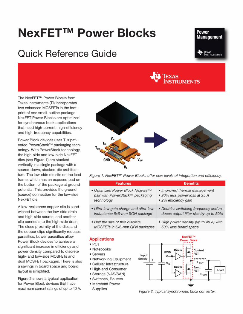
The NexFET™ Power Blocks from Texas Instruments (TI) incorporates two enhanced MOSFETs in the footprint of one smalloutline package. NexFET Power Blocks are optimized for synchronous buck applications that need highcurrent, highefficiency and highfrequency capabilities.
Power Block devices uses TI’s patented PowerStack™ packaging technology. With PowerStack technology, the highside and lowside NexFET dies (see Figure 1) are stacked verti cally in a single package with a sourcedown, stackeddie architecture. The lowside die sits on the lead frame, which has an exposed pad on the bottom of the package at ground potential. This provides the ground (source) connection for the lowside NexFET die.
A lowresistance copper clip is sandwiched between the lowside drain and highside source, and another clip connects to the highside drain. The close proximity of the dies and the copper clips significantly reduces parasitics. Lower parasitics allow Power Block devices to achieve a significant increase in efficiency and power density compared to discrete high and lowside MOSFETs and dual MOSFET packages. There is also a savings in board space and board layout is simplified.
Figure 2 shows a typical application for Power Block devices that have maximum current ratings of up to 40 A.
Power Management
Features Benefits
•OptimizedPowerBlockNexFET™pairwithPowerStack™packagingtechnology
•Improvedthermalmanagement•20%lesspowerlossat25A•2%efficiencygain
•Ultra-lowgatechargeandultra-low-inductance5x6-mmSONpackage
•Doublesswitchingfrequencyandre-ducesoutputfiltersizebyupto50%
•HalfthesizeoftwodiscreteMOSFETsin5x6-mmQFNpackages
•Highpowerdensity(upto40A)with50%lessboardspace
InputSupply +
CIN
PWM
Driver
Driver
SyncFET
ControlFET
COUT
Load
NexFET™Power Block
LOUT
Figure2.Typicalsynchronousbuckconverter.
Figure1.NexFET™PowerBlocksoffernewlevelsofintegrationandefficiency.
Applications• PCs • Notebooks• Servers• Networking Equipment• Cellular Infrastructure• Highend Consumer• Storage (NAS/SAN) • Switches, Routers• Merchant Power
Supplies

2NexFET™ Power Blocks Texas Instruments 4Q 2011
NexFET™ Power Blocks
NexFET Power Blocks are Capable of 93% Efficiency
Compared to discrete and traditional dual MOSFETs, the PowerStack package configuration in Figure 3 greatly reduces the parasitic inductance and resistance at the lowside NexFET sourcetoground connection and at the lowside drain and highside source (switchnode) connections. This inherent improvement is due to the
Figure 3. PowerStack™ technology nearly eliminates troublesome parasitics.
Figure 4. Efficiency comparison between Power Block device and discrete MOSFETs.
PWMDriver
Load
Driver
SwitchNode
LSource
LSource
LDrain
LOUT
IL
CIN
COUT
High-SideFET
Low-SideFET
InputSupply(VIN)
LDrain
Output Current (A)
Effi
cien
cy (%
)
0
94
93
92
91
90
89
88
87
86
85
845 10 15 20 25
VIN = 12 V, VGS = 5 V,VOUT = 1.3 V, fSW = 500 kHzLOUT = 0.3 µH, TA = 25°C
CSD87350Q5DCSD16404x1, CSD16321x1
Power Block
Discrete
copper holddown clips and the much shorter connection distance between high and lowside NexFET dies.
Figure 4 shows that by eliminating the parasitic inductance and resistance that are typically associated with high and lowside MOSFETS in a synchronous buck converter, higher efficiency can be achieved compared to discrete MOSFETs. Efficiency peaks at over 93% and is 90.7% at 25 A. The
lower parasitics and high conductivity of the copper clips also mean that a converter with a Power Block device can switch faster and work at higher frequencies because of the reduced switching losses.
For more information, please refer to the application note “Power Loss Calculation with Common Source Inductance Consideration for Synchronous Buck Converters” at www.ti.com/lit/slpa009
3NexFET™ Power Blocks Texas Instruments 4Q 2011
NexFET™ Power Blocks
NexFET™ Power Block Devices
Device ChannelVDS(V)
VGS(V)
Power Loss(W)
Ploss Current(A)
Max Current(A)
High Duty-Cycle Applications Package
PowerStack™ Package TechnologyCSD86330Q3D N 25 10 1.9 15 20 No SON 3x3 Power Block
CSD86350Q5D N 25 10 2.8 25 40 No SON 5x6 Power Block
CSD87330Q3D N 30 10 2.0 15 20 No SON 3x3 Power Block
CSD87331Q3D N 30 10 1.3 10 15 No SON 3x3 Power Block
CSD87350Q5D N 30 10 3.0 25 40 No SON 5x6 Power Block
CSD87351Q5D N 30 10 2.5 20 32 No SON 5x6 Power Block
CSD87352Q5D N 30 10 1.8 15 25 No SON 5x6 Power Block
CSD87353Q5D N 30 10 3.3 25 40 Yes SON 5x6 Power Block
For more information, visit www.ti.com/nexfet
NexFET™ Power Blocks and PowerStack™ Technology Optimize Board Layout and Improve System Performance
Since many highperformance computing and telecommunications products are migrating to smaller form factors, reducing board space is a primary objective. The Power Block package is half the size of two discrete MOSFETs of equivalent performance.
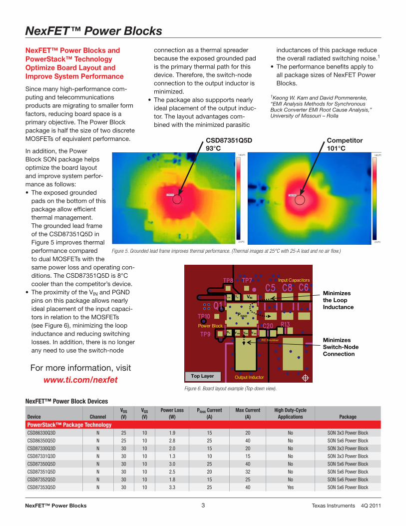
In addition, the Power Block SON package helps optimize the board layout and improve system performance as follows:• The exposed grounded
pads on the bottom of this package allow efficient thermal management. The grounded lead frame of the CSD87351Q5D in Figure 5 improves thermal performance compared to dual MOSFETs with the same power loss and operating conditions. The CSD87351Q5D is 8°C cooler than the competitor’s device.
• The proximity of the VIN and PGND pins on this package allows nearly ideal placement of the input capacitors in relation to the MOSFETs (see Figure 6), minimizing the loop inductance and reducing switching losses. In addition, there is no longer any need to use the switchnode
Figure 6. Board layout example (Top-down view).
connection as a thermal spreader because the exposed grounded pad is the primary thermal path for this device. Therefore, the switchnode connection to the output inductor is minimized.
• The package also suppports nearly ideal placement of the output inductor. The layout advantages combined with the minimized parasitic
Minimizesthe LoopInductance
MinimizesSwitch-NodeConnection
Top Layer
Figure 5. Grounded lead frame improves thermal performance. (Thermal images at 25°C with 25-A load and no air flow.)
CSD87351Q5D93°C
Competitor101°C
inductances of this package reduce the overall radiated switching noise.1
• The performance benefits apply to all package sizes of NexFET Power Blocks.
1KeongW.KamandDavidPommerenke,“EMIAnalysisMethodsforSynchronousBuckConverterEMIRootCauseAnalysis,”UniversityofMissouri–Rolla

The platform bar, E2E, NexFET and PowerStack are trademarks of Texas Instruments. All other trademarks are the property of their respective owners.
© 2012 Texas Instruments IncorporatedPrinted in U.S.A. by (Printer, City, State) SLIT127
TI Worldwide Technical Support
InternetTI Semiconductor Product Information Center Home Pagesupport.ti.com
TI E2E™ Community Home Pagee2e.ti.com
Product Information CentersAmericas Phone +1(972) 644-5580
Brazil Phone 0800-891-2616
Mexico Phone 0800-670-7544
Fax +1(972) 927-6377 Internet/Email support.ti.com/sc/pic/americas.htm
Europe, Middle East, and AfricaPhone European Free Call 00800-ASK-TEXAS (00800 275 83927) International +49 (0) 8161 80 2121 Russian Support +7 (4) 95 98 10 701
Note: The European Free Call (Toll Free) number is not active in all countries. If you have technical difficulty calling the free call number, please use the international number above.
Fax +(49) (0) 8161 80 2045Internet www.ti.com/asktexasDirect Email [email protected]
JapanPhone Domestic 0120-92-3326
Fax International +81-3-3344-5317 Domestic 0120-81-0036
Internet/Email International support.ti.com/sc/pic/japan.htm Domestic www.tij.co.jp/pic
AsiaPhone International +91-80-41381665 Domestic Toll-Free Number Note: Toll-free numbers do not support
mobile and IP phones. Australia 1-800-999-084 China 800-820-8682 Hong Kong 800-96-5941 India 1-800-425-7888 Indonesia 001-803-8861-1006 Korea 080-551-2804 Malaysia 1-800-80-3973 New Zealand 0800-446-934 Philippines 1-800-765-7404 Singapore 800-886-1028 Taiwan 0800-006800 Thailand 001-800-886-0010Fax +8621-23073686Email [email protected] or [email protected] support.ti.com/sc/pic/asia.htm
A011012
Important Notice: The products and services of Texas Instruments Incorporated and its subsidiaries described herein are sold subject to TI’s standard terms and conditions of sale. Customers are advised to obtain the most current and complete information about TI products and services before placing orders. TI assumes no liability for applications assistance, customer’s applications or product designs, software performance, or infringement of patents. The publication of information regarding any other company’s products or services does not constitute TI’s approval, warranty or endorsement thereof.