nited states patent [193
TRANSCRIPT

nited States Patent [193
Cuk et al.
[54] DC-TO-DC SWITCHING CONVERTER
[75] Inventors: Slobodan M. Cuk, Huntington Beach; Robert D. Middlebrook, Pasadena, both of Calif.
[73] Assignee: California Institute of Technology, Pasadena, Calif.
[21] Appl. No.: 837,532
1221 Filed: Sep. 28, 1977
[51] Int. C l . 2 ............................................ H02M 3/335 [52] US. C1. ......................................... 363/16; 363/40 [58] Field of Search .................... 336/184; 363/15, 16,
363/20, 21, 40, 106, 110, 124, 131, 140
~561 References Cited U.S. PATENT DOCUMENTS
3,381,202 4/1968 Loucks et al. ......................... 363/21 4,024,452 5/1977 Seidel ..................................... 363/15
Primary Examiner-William M. Shoop
Attorney, Agent, or Firm-Freilich, Hornbaker, Wasserman, Rosen & Fernandez
ABSTRACT [571 A dc-to-dc converter having nonpulsating input and output current uses two inductances, one in series with the input source, the other in series with the output load. An electrical energy transferring device with storage, namely storage capacitance, is used with suit- able switching means between the inductances to DC level conversion. For isolation between the source and load, the capacitance may be divided into two capaci- tors coupled by a transformer, and for reducing ripple, the inductances may be coupled. With proper design of the coupling between the inductances, the current rip- ple can be reduced to zero at either the input or the output, or the reduction achievable in that way may be divided between the input and output.
33 Claims, 28 Drawing Figures
SIGNAL SOURCE I I I
https://ntrs.nasa.gov/search.jsp?R=20080004199 2018-02-12T16:54:29+00:00Z
E
t Jan* 15, 1980 Sheet 1 of 10 4,184,
PRIOR A R T
T
P R I O R A R T
. 3 SWITCH SWITCH DRIVE DRIVE
P R I O R A R T

. Patent ~a. 15,1980 Sheet 2 of 10
SWITCHING S IGNAL
SOURCE
TRANSISTOR ON I N T E R V A L TsD
TRANSISTOR ON I N T E R V A L TsD
T R A N S I S ~ O ~ OFF I N T E R V A L T,D f Ts(l-D)
iI a n d i2 nonpolsating currents w i t h ripple

Sheet 3 of 10 4,184,d
20
c

Vr
0 -
LI
Sheet 4 of 10
V L2
9
t
\ V
/
FIG. 7
V D v,= 0’ FIG.

Sheet 5 of 10 4, ]I 84, P

a Patent Jan. 15, 1980 Sheet 6 of 10 9 89
1 FIG. 8 a

t Jan. 15, I980 Sheet 7 of 10
I SWITCHING VOLTAGE S O U R C E
20

Sheet $‘of 10
vgl =
20
I: N
SWITCHING - VOLTAGE - 4 SOURCE 1
2 FIG. I P

Sheet 9 of 10
s w ITCH l N G VOLTAGE
26 L SOURCE
1302
4- I 7-
04
_, ... /
I
114 J

U.S. Patent ~ m . 15, 1980
. I
Sheet 10 of 18 9
I
SWITCHING VOLTAGE S O U R C E
‘104

4.184.197 1
DC-TO-DC SWITCHING CONVERTER
ORIGIN O F THE INVENTION The invention described herein was made in the per-
formance of work under a NASA contract and is sub- ject to the provisions of Section 305 of the National Aeronautics and Space Act of 1958, Public Law 85-568 (72 Stat. 435; 42 USC 2457).
BACKGROUND OF THE INVENTION This invention relates to dc-to-dc converters and
more particularly to a switching converter having non- pulsating input and output current.
Several of the prior-art dc-to-dc converters are de- scribed here and some of their deficiencies are dis- cussed. Later, after the present invention disclosed herein has been described, comparison of the invention with the prior-art converters will reveal the superior characteristics of the invention.
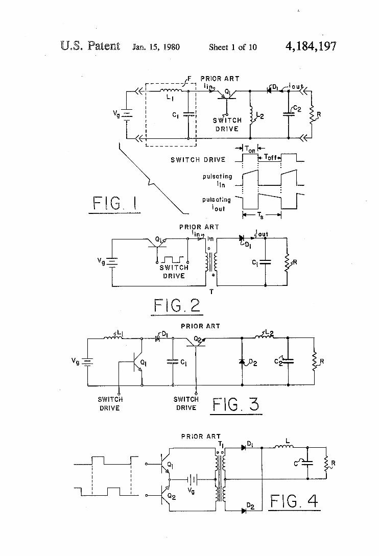
All of the three configurations discussed here (con- ventional buck-boost, cascade connected boost and buck, and double-ended, push-pull converters) have the general DC conversion property, that is increase or decrease of both DC voltage and current. The same property is present in this invention as well, but with nonpulsating input and output current, and if desired isolation between the input and output can be obtained. The input or output current ripple may be reduced to zero.
OBJECTS AND SUMMARY OF THE INVENTION
An object of this invention is to provide a dc-to-dc converter having a maximum performance (high effi- ciency and low electromagnetic interference) for the minimum number and size of parts.
A further object is to provide a dc-to-dc converter having nonpulsating input and output current.
Another object is to provide a dc-to-dc converter with input or output current ripple reduced to zero.
Still another object is to provide a dc-to-dc converter which satisfies any of the foregoing objects with isola- tion between the current source and the load.
Yet another object is to provide a dc-to-dc converter which satisfies any of the foregoing objects with or without isolation and with an extended range of step-up or step-down of the input DC voltage.
These and other objects of the invention are achieved in a dc-to-dc converter with two inductances, a first one
2 no ripple in either the input current or the output cur- rent. For zero output current ripple, the transformer is designed for the condition n=k, and for zero input current ripple, the transformer is designed for the con- dition h = l / k , where n is equal to the square root of the ratio of the self-inductances L1 I and L.22 of the input and output windings, respectively, and k is the coupling coefficient between the two windings. Alternatively, either of the two inductances may be a tapped inductor to form an autotransformer. In the input, the autotrans- former provides an extended range of step-up of the input DC voltage, and in the output it provides an ex- tended range of step-down of the input DC voltage.
The novel features that are considered characteristic of this invention are set forth with particularity in the appended claims. The invention will best be understood from the following description when read in connection with the accompanying drawings.
BRIEF DESCRIPTION OF THE DRAWINGS FIG. 1 is a schematic diagram of a conventional
FIG. 2 is a schematic diagram of a conventional
FIG. 3 is a schematic diagram of a conventional cas-
FIG. 4 is a schematic diagram of a conventional push-
FIG. 5 is a schematic diagram of an embodiment of the invention illustrating and idealizing its switching means, FIGS. §(I) and 5(2) illustrate configurations of the circuit of FIG. 5 with its switch to the left and to the
35 right, respectively, FIG. 5a shows the circuit of FIG. 5 with a bipolar transistor and diode used to implement the ideal switch, and FIGS. 5b and 5c show variants of the circuit of FIG. 5.
FIG. 6 is a waveform diagram illustrative of wave-
FIG. 7 is a waveform diagram illustrating a voltage waveforms occurring on input and output inductors.
FIG. 8 is a circuit diagram illustrative of a second 45 embodiment of the invention, and FIGS. 8a and 86
show variants of the circuit in FIG. 8. FIGS. 8(1), 8(2) and 8(3) are waveform diagrams illustrating the effects of inductive coupling design between input and output inductances in the present invention, and FIG. 8(4) is a
50 generalized circuit diagram of this inductive coupling.
15
20
buck-boost converter.
25 transformer-coupled buck-boost converter.
caded boost converter followed by a buck converter.
30 pull switching dc-to-dc converter.
40 forms occurring in the circuit of FIG. 5.
in series with the input source and a second one in series FIG. 9 is a circuit diagram of a variant of the inven- with the load, and energy transferring means having tion shown in FIG. 50 using VMOS switching, and storage capabilities connected between the two induc- FIGS. 90 and 96 are variants of FIG. 9. tanCeS. The energy transferring meanS is comprised Of FIG. pQ is a circuit diagram of another embodiment storage capacitance in series with the two inductances 55 of the invention in FIG. sa which provides for DC and switching means for alternately connecting the isolation. junction between the first inductance and the storage FIG. is a circuit diagram of a variant of the circuit capacitance to ground for the source, and connecting of the junction between the storage capacitance and the FIG. I2 is a circuit diagram of an embodiment of this second inductance to ground for the load. In some ap- 60 . plications, both the load and the source may be refer- enced to the Same ground. those applications where FIG. 13 is a circuit diagram of an embodiment of the the load and the may not be referenced to a invention having multiple outputs with isolation and common ground, isolation between the source and the coupled inductors. load is provided by dividing the storage capacitance 65 FIG. 14 illustrates a variant Of the circuit of FIG. 10 between two capacitors with transformer coupling be- where the isolation transformer is replaced by an auto- tween the capacitors. In either case, the two induc- transformer with multiple output taps. tances may be windings of a transformer designed for FIG. 15 illustrates a variant of the circuit of FIG. 13.
having outputs.

4,184,197 3 6
is shown in FIG. 3 wherein corresponding elements are DESCWIPT1oN OF ”IQR ART CoNVERTERS identified by like reference numbers as in FIGS. 1 and 2,
A conventional buck-boost converter is shown in but with subscripts 1 and 2 for the two basic converters PIG. 1 together with the corresponding pulsating input cascaded. and output current waveforms, i,, and io”!. As seen in 5 While this converter has some good properties (both FIG. 1, the current drawn by this DC converter is not input and output currents continuous, that is, nonpulsat- COntinUOUS and “clean” DC; rather it iS pulsating, ing) it has some additional deficiencies. It needs an addi- where the Pulse amplitude in a higher c ~ r e n t (and tional transistor Q2 and diode ID2 which cause added Power) application may be very high. This invariably DC and switching losses and hence significantly de- requires that an input filter F (usually a Single section 10 grade the efficiency of the converter, besides its in- low”pass filter comprised of an inductance L1 and ca- crease of complexity and number of components. Also pacitance 61) be put in front to smooth Out the substan- at least one ofthe switching transistors requires floating
drawn from the line electromag- cuits, which further complicates its drive, Also there is netic interference problems generated by the 15 no possibility to introduce the isolation property into
in the
tial current pulse Component at the Switching frequency drive circuitry, hence need for two isolated drive cir- In that
variation in energy flow (pulsating current) are this converter by simple means, as was the reduced, and contamination of the environment by the undesired electromagnetic disturbances is alleviated. In operation, a transistor Q1 is alternately turned on and
energy, and while it is off, the energy stored flows
the load smooths the output current to the load.
conventional buck-boost converter of FIG. 2. Another commonly used variation of the conven-
arrangement of the two converters in FIG. 2 is shown
identified by like reference characters as in FIG. 2 but while the input filter F reduces EMI problems at the with subscripts 1 and 2 for the two basic converters
input, the output current io,,*, as seen in FIG. 1, is still 25 working in Parallel and a single Output and c. pulsating, thus requiring a large size of output capaci- This typical push-pull type converter circuit gener- tance C2 to smooth out that pulsating current ripple. In ally requires many circuit components in addition to addition, relatively complicated “floating” switch drive those shown to compensate for the inherently disadvan- circuitry is required for the transistor in this converter tageous characteristics of the converter circuit. For since its emitter is not referenced to ground. 3o example, the input impedance of the conventional push-
In summary, the important deficiencies of this prior pull converter tends to be capacitive causing large in- art include the fact that both input and output currents rush currents when the circuit is initially energized. are pulsating (with corresponding EM1 problems), that Also in this converter, peak transient voltages and cur- larger size and weight are required, that complicated rents occur owing to the conduction discontinuity drive circuitry is required and, as demonstrated later, 35 when both switching transistors are biased nonconduct- that significantly lower efficiency results. ing. Large capacity switching transistors and converter
The converter of FIG. 1 can be easily updated to power transformer are required to deal with these peak obtain a converter with a so-called isolation property transient currents and voltages. In addition, symmetry that allows the unregulated source voltage ground to be correction is frequently necessary to prevent the trans- isolated from the load ground. Such a modified trans- former from drifting into saturation owing to unequal former-coupled buck-boost converter is shown in FIG. parameter characteristics of the two switching transis- 2, wherein corresponding elements are identified by like tors. This converter normally requires an input filter reference characters as in FIG. 1. which still further increases its already high complexity.
voltage gain (vns) of the Many of the disadvantages and the deficiencies out- converter in FIG. P is given by: 45 lined in these converters are overcome by the present
invention and in several of its extensions as verified both theoretically and experimentally in the later compari- son.
DESCRIPTION O F PREFERRED EMBODIMENTS
FIG. 5 is a schematic diagram of a preferred embodi- ment of the invention. A DC input voltage (V,) source I O has its positive terminal connected to an input induc-
Hence, an additional control Over the step-up or step- 55 tance 12. The input inductance is connected to a storage down ofthe voltage can be achieved by the transformer capacitance 14. An idealized switch 16 is provided for turns ratio n. alternately connecting the junction between the first
Note also the reversal of the output voltage polarity inductance 12 and storage capacitance 14, and connect- in the converter of FIG. 1 since it is inherently invert- ing the junction between the latter and a second induc- ing, while that of PIG. 2 can have either polarity de- 60 tance 18, to the common point between the source and pending on the direction of coupling of the transformer the load. The second inductance 18 is connected in (dot sign), and corresponding direction of the diode D1. series with the load 20. Filter capacitance 22 is con-
The same general DC conversion function of Equa- nected across the load. tion (1) can be achieved by simply cascading the two FIG. 5(1) illustrates the circuit configuration with the basic converters, namely the boost (with 65 switch to the left and FIG. 5(2) illustrates the circuit V V S = l /D=DC gain) and the buck (with configuration with the switch to the right. Assume that V/Vg=D=DC gain) resulting in the same overall DC the switch is initially to the right as in FIG. 5(2). Then, gain as given by Equation (I). This suggested converter capacitance 14 charges up from the source BO through
off. When it is conducting, an inductance L2 stores 2o tional buck-boost converter which
through a diode D1 to a load R. A capacitance Czacross
a Push-pul1
in 4, where again corresponding elements are
Note that the ideal
(I)
where Dzduty ratio (ratio of the on-time to the switch- ing period Ts), or D= Ton/Ts, and D’ is the complemen- tary duty ratio, TO~/Ts. The corresponding gain of the 50 converter in FIG. 2 is:
V/Vg= n ( D / D ) .
V/Vg= D/D:D = 1 - D,
(2)

4,184,197 5
inductance 12, When the switch 16 is thrown to the left, inverting converter as is the conventional converter of it connects to ground the positive side of capacitance 14 FIG. 1. as shown in FIG. 5(1). As a result, capacitance 94 dis- Some simple modifications of the new converter that charges through inductance 18 into the load 20 and are also applicable to the conventional buck and boost charges capacitance 22. When the switch is then thrown fi converters can now easily be made. Namely by tapping back to the right, capacitance 14 again commences to the input inductor in the new converter of FIG. 5 (as charge up while inductance 18 supplies the load cur- shown in FIG, 56 ), an additional step-up of the input rent. Thus it is evident that as the switch 16 is operated DC voltage dependent on the tap ratio ntmay be alternately to the left and to the right, the Capacitance achieved, Likewise, by tapping the output inductor in 14 and inductance 18 will Supply Current to the load. 10 the converter of FIG. 5, as shown in FIG. Sc, an addi- The capacitance 22 aids the inductance, thereby filter- tional step down of the input DC voltage is provided ing the output current ripple. through this autotransformer action.
signal from the switching source 26. Waveform B repre- FIGS, 56 and sC are then sents the input current il from the source, and waveform 15
input and output currents are seen to have a ripple, but
the prior art. (See FIG. 1.)
switch 16 implemented by a transistor 23 and a diode 24. In operation, assume that the transistor is initially in its nonconductive state. Then capacitance 14 charges from the source 10 through the inductance since the diode 24 is forward-biased. At this time the collector of the tran- 25 sistor is positive with respect to its emitter so that when a switching pulse arrives to turn on the transistor, it becomes conductive. This has the effect of grounding the side of the capacitance that iS connected to the transistor. The diode is thus back-biased, and the capaci- 30 and vLz on the two inductances 12 and tance discharges through the inductance 18 into the
sistor is cut off, the storage capacitance 14 again charges while the output inductance 18 supplies current to the
from a source 26 while the diode 24 responds as a com- plementary switch to the transistor being switched off and on.
FIG. 6 shows in waveform A an on-off switching The overall ideal DC gains of the two converters in
C represents the output inductor current iz. Both the
neither is pulsating (periodically falling to zero), as in
V/Vg=nl(D/D’) (tapped input inductor)
V/Vg=( l/n,)(D/D’) (tapped output inductor)
(5)
(6)
FIG. Sa shows the circuit of FIG. 5 with the idealized 20 where the tap ratio nt is as defined in FIG. 56 or FIG. 5c. These two relatively straightforward modifications are useful when a large step-up, or seep-down, ratio of the input voltage is required, The tap ratio nt can be chosen to be less than unity if desired.
Besides these relatively simple modifications, Some rather crucial extensions can be made by utilizing unique possibilities of the new converter topo~ogy, as shown next.
Consider, for example, the voltage waveforms vL1 as defined in
FIG. 5, They can easily be found by the fact that the load. When the switching pulse drops SO that the tran-
load. Thus the transistor is driven by a train of pulses 35
voltage on capacitance 14 is essentially a DC voltage =vg,D,. With the transistor on:
V L I = V , ‘ V ~ L ~ = V ~ ~ - V = ( V ~ / D ) - ( D V ~ / D ) = V ~ (71
With the transistor turned off:
From the foregoing it is evident that the capacitance V L ~ = Vg-(Vg/D’=-(D/D’)Vg,.V~2= - V=-(D/- 14 plays the role of an energy-transferring device. Pres- 4o D’) v g ently used converters store energy in inductance in the form of a magnetic field during one interval and release the energy to the load during a subsequent interval. In the present invention, the energy is accumulated in capacitance in the form of an electric field and then 45 transferred to a load. Owing to significantly higher energy density per unit volume (or weight) of capacitor storage compared to inductive storage, significant size reductions are possible.
mined from the following formula:
The voltage waveforms VL1 and V L ~ are then as shown in FIG. 7 which is a diagram illustrating these wave- forms.
In FIG. 7, the waveform 30 is the waveform on in- ductance n2 and the waveform 32 is the waveform on inductance 18 when the converter shown in FIG. 5 is operating. From the waveforms shown in FIG. 7, it becomes clear that the two inductances can be coupled
The DC voltage gain of the invention Can be deter- 50 as in a transformer, without affecting the basic DC conversion property provided the transformer has a one-to-one turns ratio. This is easily achieved by choos- ing a transformer having the primary and secondary winding with the same number of turns and with the
55 direction of coupling shown by dots in FIG. 8, which illustrates a variant of the invention wherein the indup- tances p4 and 18 are respectively the primary winding 34 and the secondary winding 36 of a one-to-one trans- former. Other components of the circuit which serve
60 the same function as the components on FIG. B are identified by the same reference numerals. A single-
12/11 = D / D (4) pole, double-throw switch 40 represents the functions of the diode and transistor in the circuit of FIG. 5. The switching converter shown in FIG. 8 is the only switch-
65 ing converter (besides the straightforward cascade-con- nected boost and buck converters shown in FIG. 3) in which transformer coupling of the input and output inductance is possible. In other two-inductance con-
(3) V/ Vg = D / D
where: V, is the DC input voltage D is the fractional ON-time of the transistor switch;
D’ is the fractional OFF-time of the transistor switch The DC current gain may be determined from the
and
formula:
where: 11 is the DC input current, and I2 is the DC output current
Thus, as seen from the polarity of output voltage in FIG. 5, the present invention is also an inherently-
6
9 4,184,197
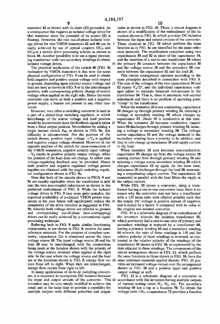
transistor 42 as shown with its drain (D) grounded. As tudes as shown in FIG. PO. There, a circuit diagram is a consequence this requires an isolated voltage drive for shown of a modification of the embodiment of the in- that transistor since the potential of its source (S) is vention shown in FIG. §a which provides DC isolation floating. However, the two out-of-phase isolated volt- between the input and output circuits of the converter. age drives for two VMOS transistors 42 and 44 can be 5 Those elements in FIG. 10 which perform the same easily achieved by use of optical couplers OCA and function as in FIG. §a are identified by the same refer- OCB in a switch drive processing scheme as shown in ence numerals. The modification comprises using two block 46. Another possibility is to use a signal process- capacitances 50 and 52 in place of the capacitance 14, ing transformer with two secondary windings to obtain and the insertion of a one-to-one transformer 54 where isolated voltage drives. 10 the primary 56 connects between the capacitance 50
The practical implication of the switch 40 (FIG. 8) and the voltage source PO and the secondary 58 con- realization by VMOS transistors is that now the same nects between the capacitance 52 and the load 20. physical configuration of FIG. 9 can be used to obtain This circuit arrangement operates according to the both negative and positive output voltage with respect same principles described in connection with FIG. 5. to ground, depending upon whether source voltage and 15 The sum of the voltages of the two capacitances 50 and load are used as shown in FIG. 9 or in the interchanged 52 equals Vg/D’, and the individual capacitance volt- position, with corresponding polarity change of source ages adjust to maintain balanced volt-seconds in the voltage when applied on the right side. Hence the same transformer 54. That is, there is automatic volt-second converter can serve as both a positive and a negative adjustment and there is no problem of operating point power supply, a feature not present in any other con- 20 “creep” in the transformer. verter. When the transistor 23 is not conducting, capacitance
However, very often a switching converter is used as 50 charges up through primary winding 56, inducing a a part of a closed-loop switching regulator, in which voltage in secondary winding 58 which charges up interchange of the source voltage and load position capacitance 52. Diode 28 is conductive at this time. would be inconvenient since the feedback signal is taken 25 When the transistor 23 becomes conductive, capaci- from a fixed output position. Nevertheless by adding a tance 50 discharges through primary winding 54, induc- single manual switch SM, as shown in FIG. 9a, this ing a voltage in secondary winding 58. The voltage difficulty is circumvented. For the position of the across capacitance 52 and the voltage induced in the switch shown, positive input voltage +Vg is applied secondary winding have a polarity to be additive, and and negative output voltage obtained. However in the 30 they in turn charge up inductance 18 and supply current opposite position of the switch for cross-connection of to the load. the VMOS transistors, negative polarity input voltage When transistor 23 next becomes non-conductive, -Vg results in positive polarity output voltage, while capacitance 50 charges up from the voltage source BO the position of the load does not change. In either case causing current flow through primary winding 56 and voltage-regulating feedback may be provided. Hence 35 inducing a voltage across secondary winding 58 which both positive and negative regulated voltage power charges capacitance 52 up again. At the same time, supplies are obtained with the single switching regula- inductance 18 discharges through the load 20, maintain- tor configuration shown in FIG. 9a. ing a nonpulsating output current. The capacitance 22
Note that both of the circuits shown in FIGS. 9 and connected in parallel with the load filters the ripple in k are equally applicable when the transformer is split 40 the output current. into the two non-coupled inductances as shown in the While FIG. 10 shows a converter, using a trans- preferred embodiment of FIG. 5. While the isolated former having a one-to-one conversion ratio, there is no voltage drives in FIG. 9 may seem quite complex, the reason why the converter may not have a transformer expected availability of p-channel VMOS power tran- with a 1:N turns ratio with relative polarity such that sistors in the near future will significantly reduce the 45 the output DC voltage is positive instead of negative, complexity of the drive circuitry as suggested in FIG. and is scaled by a factor N compared with its value in 9b, wherein both voltage drives are referred to ground the original non-isolated converter. and corresponding out-of-phase (non-overlapping) FIG. 11 is a schematic diagram of an embodiment of drives can be easily achieved by a conventional signal the invention wherein the isolation transformer 54, processing technique. 50 which previously had a one-to-one ratio of primary and
Referring back to FIG. 9 again, similar functioning secondary windings is replaced by a transformer 619, components, as are shown in FIG. 8, receive the same having a primary winding 62 and a secondary winding reference numerals. For the purpose of complete sym- 64 wherein the ratio of these windings is 1:N and the metry, capacitance 22a is connected across the input relative polarity of these windings is reversed, as con- voltage source 10. The input voltage source PO and the 55 trasted to the relative polarity of the windings of the load 20 may be interchanged, with the connections transformer 54 shown in FIG. BO, as represented by the being made at the location shown with the polarity of dots adjacent to these windings. The components of the the voltage source reversed when applied at the right circuit arrangement shown in FIG. BE, which perform side. In the case where the voltage source and the load the same functions as those shown in FIG. 10, have the are at the locations shown in FIG. 9, energy flow oc- 60 same reference numerals applied thereto. FIG. BB pro- curs from left to right. When they are interchanged, vides an’increased voltage output over the arrangement energy flow occurs from right to left. shown in FIG. 10 and a positive input and positive
In many applications of dc-to-dc switching convert- output voltage as well. ers, it is necessary to incorporate DC isolation between FIG. 12 is a schematic diagram of a converter in the input and output circuits of the converter. This 65 accordance with this invention having multiple outputs invention may be very simply modified to achieve this of various scaling ratios N1, N2, etc. The secondary result and at the same time to provide a capability for winding 68 has a tap at a location 70. To obtain the multiple outputs with different polarities and magni- voltage ratio 1:N1, a capacitance 72 provides a function

analogous to that of capacitance 52 in FIG. 80. An since the same winding is part of both primary and inductance 74 produces a function analogous to that of secondary windings. However, the isolation property is inductance 18. Diode 76 is connected between the tap, lost. 70 and the junction between capacitance 72 and induc- FIG. I5 illustrates another variation of a dc-to-dc tance 74 and performs a function analogous to diode 24. 5 converter with an isolation transformer as in FIG. 13 Capacitance 78 is connected across the load 8Q and and coupling of both output inductances back to the performs the function analogous to the one performed input inductance, as in FIG. 13 with tapping of the input by capacitance 22. and/or output inductances for extension of step-up and-
Similarly, to obtain the voltage ratio l:Nz, connection /or step-down voltage ranges as in FIGS. 5b and 5c. is made to a tapping point 82. The circuit is the same as 10 Here the input inductance winding 130 is tapped for described, including the capacitance 84 connected in extended step-up range and one output inductor wind- series with an inductance 86. A diode 88 connects the ing is tapped for an extended step-down range. While junction of capacitance 84 and inductance 86 to the such an arrangement of both step-up and step-down tapping point 70. A capacitance 90 is connected across range extensions in a single converter of a multi-con- the load 92. 15 verter circuit is not likely to be required for any applica-
To obtain the voltage ratio l;N3, capacitance 94 is tion, it does serve to illustrate tapping the coupled input connected in series with inductance 96. Diode 98 is and/or output inductances in a multi-converter configu- connected between the junction of the capacitance and ration. the inductance to the tap off point 70. Capacitance PO0 The new converter topology described with refer- is connected across the load 102. 20 ence to FIG. 5, and its various extensions and modifica-
FIG. 13 shows an embodiment of the invention wherein isolation between input and output is provided as well as coupling of both output inductances back to the input inductance. The isolation is achieved using transformer 104, wherein the secondary winding 106 has a tap at a point 108, to provide two ratios I:N1 and 1:Nz. There is a capacitance 110 connected in series with an inductance 112. A load I14 is connected to receive the output of the entire secondary winding 106 and a capacitance 114 is connected across the load. A diode 118 is connected between the junction of capaci- tance 110 and inductance 112, and the load.
For the second output, capacitance 120 is connected in series with an inductance 122. Inductance 122 is con- nected to the other end of the winding 106 through a load 124. Capacitance 126 is connected across the load and diode 128 is connected between junction of capaci- tance 120 and inductance I22 and the other side of the load. The distinction between the circuit arrangement shown in FIG. 13 from the one shown in FIG. 12 is that the input inductance 130 is coupled to the respective output inductances 112 and 122. For maximum ripple reduction and minimum size and weight, the inductance coupling ratio should be the same as the respective isolation transformer ratios for each output; however, benefits intermediate between the non-coupled induc- tances and equal ratio-coupled inductances can be ob- tained by use of unequal ratios.
tions have been experimentally verified, and an exten- sive comparison, both theoretical and experimental, has been made between them and the prior art described with reference to FIGS. 1-4. The significant advantages
25 of higher efficiency, smaller size and weight, and signifi- cantly reduced switching ripple are realized in addition to a number of other advantages. A discussion of the highlights of these comparisons and advantages follows.
First, a comparison between the new converter of 30 FIG. 5 and the conventional buck-boost converter to
which an input filter is added (FIG. I) is made. As seen in FIGS. 1 and 5, both converters consist of the same components, but differ in the way these components are interconnected. The two experimental test circuits for
35 the converters of FIG. 1 and FIG. 5a have been built with the following element values: L1=6.5mH,L2=3.5mH,C1=100pF,C2=0.47pF,
Tests which have been made show that this invention 40 (FIG. 5) provides not only a larger DC gain, but also
significantly higher efficiency throughout the duty ratio D range. For example, for the typical application, where the input voltage is V,=5 V and the output voltage kept constant at V = 15 V by closed-loop regu-
45 lation, the converter, in accordance with this invention, would operate at 93.5% efficiency while the converter of prior art operates at only 65.5% efficiency. This difference is actually even bigger since, for the same
R=75R
Note that in the -isolated switching converters of conditions, the transistor and diode DC losses would be FIG. 10 and FIG. 11, the bipolar transistor and diode 50 about 30% higher in the conventional circuit. Similarly, combination can again be substituted by the combina- transistor switching losses would be significantly tion of two VMOS power transistors as previously higher, further degrading the efficiency of the conven- shown in FIG. 9. However, to preserve the isolation tional circuit. Finally, the output current of the conven- property of the converter the isolated voltage drives of tional circuit is pulsating, causing significant power loss FIG. 9 should be implemented. Hence, the single con- 55 in the ESR (equivalent series resistance) of the output figuration can be used (with addition of manual switch capacitor, especially at higher load current, which is SM) to obtain both positive and negative, isolated, regu- not the case for the converter constructed in accor- lated output voltages. dance with this invention. When the switching ripple
Note also that if the multiple output feature is desired was compared for the two converters, it was substan- without the need for the isolation, a simple modification 60 tially reduced by the new converter. In fact, there was of the basic isolated version of FIG. BO can be made. a 30:1 ripple reduction. Weight and size reduction are Namely, by use of an autotransformer 60 with several also achieved owing to the significant energy-transfer- secondaries, (tap-off points) instead of the isolation ring capabilities per unit size and weight of the capaci- transformer in FIG. BO, the converter of FIG. 14 is tive storage in energy transferring (commutating) ca- obtained. The advantage of using the configuration of 65 pacitance CI. Thus, when C1 was reduced 1000 times, to FIG. 14 is the same as that coming from replacement of CI =O. 1 pF the output switching ripple remained virtu- an isolation transformer by an autotransformer, namely, ally unchanged. Also note that the element values the reduction in the size and weight of the transformer chosen are such as to show only moderately the advan-

4,184,197 3 14
tages of this invention, since at higher load current they with a “single-ended’’ transformer in which automatic are even more pronounced. volt-second balance is obtained by self-adjustment of
In yet another comparison, the conventional con- the voltages on the capacitors 50 and 52; there is no DC verter of FIG. 1 required special floating drive circuitry path in any winding. to drive its power transistor Q1, while there was no such 5 In summary, a novel dc-to-dc converter is developed requirement in the new converter whose power transis- which offers higher efficiency, lower output voltage tor is referred to ground. ripple, reduced EMI, smaller size, and yet at the same
It is now appropriate to compare the coupled indue- time achieves the general conversion function: it is ca- tor extension Of the new converter 8, with a pable of both increasing or decreasing the input voltage simple transformer-coupled version (FIG. 2 ) of the 10 depending On the duty ratio of the transistor switch. conventional buck-boost converter in FIG. I. As seen in This converter employs a new circuit topo~ogy which
and $9 both converters consist Of the Same enables it to have both input and output current nonpul- components: a single transformer, capacitance c1 pacitance C2 is not essentia1 for the proper Operation Of
sating. The converter uses capacitive energy transfer rather than the inductive energy transfer employed in the new converter in FIG. a), and a single switch real- 15 the prior art.
ized by the bipolar transistor-and-diode combination. However, while both converters have the simplest pos- sible structure, the new converter of FIG. 8 has several important advantages. For example, the “flyback” con- verter of FIG. 2 has both the output and the input cur- 20 rent pulsating, with resulting very poor ripple perfor-
(FIG. 8) has switching current and voltage ripples sub-
in FIG. $(I)) over the already small ripple in the basic 25 embodiment of FIG. 5, and current ripple may be re- 5. Substantial weight and size reduction due to duced to zero at either the input or output by proper smaller output filter and smaller energy transfer- design of the inductive coupling between the inductors, ring device (capacitance Cl). as shown in FIGS. 8(3) and 8(2), respectively. The 6. Electromagnetic interference @MI) problems are direct consequence of its nonpulsating output current is 30 substantially reduced, thanks to the small ac input also the higher voltage gain and efficiency throughout current ripple, without need for additional input the duty ratio variation as in the previous comparison. filters. In addition, the transformer in the conventional “fly- 7. Excellent dynamic response enables simple com- back” converter acts essentially as an inductor, since the pensation in a switching regulator implementation. energy is stored in the primary during one part of the 35 8. Much siompleer transistor drive circuitry, since the switching cycle, and delivered to the output through switching transistor is referenced to ground the secondary during the other part of the cycle. In the transformer of the new converter of FIG. 8, however, In addition to these advantages, the unique topology the two windings function simply as the two separate of the new switching converter allows some important original inductors for the DC current and as an AC 40 extensions to be made which are otherwise not achiev- transformer for ripple and other AC considerations. An able in conventional switching converter structures. obvious saving in both size and weight also results by placing the two inductor windings of the original con- 1. Coupling of the inductances in the new converter
further substantially reduces both input and output verter of FIG. 5 on the same core. current ripple as well as output voltage switching ripple. cascade connection of the conventional boost converter
two VMOS power transistors allows the same number of transistors and diodes in the new converter converter to achieve a dual function, and to serve of FIG. 5 (one transistor and diode less), translates into
lower DC and switching losses, hence higher effi- 50 as both a positive or a negative regulated voltage ciency, in addition to the decreased circuit complexity. Also, the transistor removed in its realization is the one 3. Insertion of a single transformer in the structure of requiring floating drive. Moreover, while the isolation and multiple output feature can be easily incorporated the new converter (FIG. IO) results in the highly
of a single transformer, this is not possible in the prior- inverted or noninverted output capability. art converter of FIG. 3. Nowever, the coupling of the Thus, the new switching dc-to-dc converter is supe- inductors may still be implemented with the resulting rior to any of the currently known converters in its ripple reduction benefits. category, outperforming them in every respect.
Accordingb’, there have been described and s h w n new converter (FIG. 10) with the usual way of achiev- herein novel and useful circuit arrangements for dc-to- ing the isolation in the buck converter by use of a push- dc converters. Although only a limited number of par- pull configuration (FIG. 4). As seen in FIG. 4, that ticular embodiments have been illustrated and de- realization requires two switches and associated drives, scribed, it is recognized that modifications and varia- and there is a problem of “creep” of the transformer 65 tions may readily occur to those skilled in the art. Con- core operating point because of imbalances in the push- sequently, it is intended that the claims be interpreted to pull symmetry. In contrast, the new converter of FIG. cover such modifications and variations. PO achieves the same results with a single switch, and
Some of the important advantages of the new con-
1. Provides true general (increase or decrease) DC and current’
2* Offers much higher efficiency.
verter Over the other existing converters are:
level conversion Of both
mance. By contrast, the coupled-inductor extension 3. Both Output and current are much
stantially reduced (by an order of magnitude as shown 4. No dissipation problems in the ESR of the output smaller.
(grounded emitter).
The additional benefits are:
In still another comparison with the straight-forward 45
by the buck converter 3)7 the reduced 2. Implementation of the ideal switch S in FIG. 9a by
supply.
in the new converter, as shown in FIG. BQ, by addition 55 desirab1e property, together with multiple
Finally, let us compare the isolated version of the 60
What is claimed is:

115 4,184,197
I. A dc-to-dc converter having both input and output current nonpulsating for applying an input voltage from e source to a load, said converter being comprised of:
path instead connects the inductor tap to the load return current path.
9. A dc-to-dc converter as defined in claim B wherein an input inductance, said switching means is comprised of a first serniconduc- storage capacitance, 5 tor switch connecting the junction between said input an output inductance, inductance and said storage capacitance to said return means connecting said input voltage Source, said current path for said source, and a second serniconduc-
input inductance, said storage capacitance, said tor switch connecting the junction between said Output output inductance, and said load in series to form a inductance and said storage capacitance to said return series circuit, said series circuit having a junction 10 current path for said load, and means for alternately between said input inductance and said storage turning said switches On. capacitance, and a junction between said storage 10. A dc-to-dc converter as defined in Claim 9 capacitance and said output inductance, and wherein said first semiconductor switch is a bipolar
switching for connecting the junc- power transistor and said second semiconductor switch tion between said input inductance and said storage l5 is a diode. capacitance, and the junction between said storage 11. A dc-to-dc converter as defined in claim 9, capacitance and said output inductance, to return wherein said switches are VMOS power transistors in
improved dc-to-dc converter is provided which rectional energy flow are preserved. 20 12. A dc-to-dc converter as defined in claim 1 has optimum topolopy and superior performance wherein said storage capacitance is divided into two properties.
wherein capacitances, and said means for connecting in series said input voltage source, said input inductance, said two capacitances, said output inductance, and said load said input inductance is a tapped inductor to form an
autotransformer, and said switching means which previ- 25 is comprised of an isolation transformer having a pri- ously connected the junction between said input induc- mary winding connected between one capacitance and tance and said storage capacitance to the source return said return current path for said and having a
itance and said return current path for said load. source return current path. 13. A dc-to-dc converter as defined in claim 12
said output inductance is a tapped inductor to form an wherein said input and output inductances are com- autotransformer, and said switching means which previ- prised of first and second inductors coupled to reduce
ductance and said storage capacitance to the load return 12, and
load return current path. transformer having an additional secondary winding for 4. A dc-to-dc converter as defined in claim B wherein the additional load and a separate storage capacitance
said input and output inductances are respective first and inductance in series coupling the additional second- and second coupled inductors, whereby current ripples ary winding of said transformer to the additional load, are reduced in at least one of two currents consisting of 40 and said switching for alternately an input current through said first inductor and an out- connecting the junction between said separate induc- put current through said second inductor. tance and storage capacitance to a return current path 9. A dc-to-dc converter as defined in claim 4 wherein for said additional load.
said first and second inductors are coupled on a core to 15. A dc-to-dc converter as defined in claim 12 form a transformer designed for the condition n = k for 45 wherein said input and output inductances are corn- zero output current ripple, where k is the couPb3 prised of an input inductor and a plurality of output coefficient and n is equal to the square root Of the ratio inductors for a plurality of loads, and said input indue- of the self inductances Lii and L2z of said first and tor is coupled to said plurality of output inductors to second inductors, respectively. reduce ripple in at least one of said input and output
said first and second inductors are coupled on a core to 116. A dc-to-dc converter as defined in claim 15 form a transformer designed for the condition n = 1/k wherein said input inductor is tapped to form an auto- for zero input current ripple where k is the coupling transformer, and said switching means which previ- coefficient and n is equal to the square root of the ratio ously connected the junction between said input indue- of the self inductances Lii and L22 of said first and 55 tance and said storage capacitance to the source return second inductors, respectively. current path instead connects the inductor tap to the
7. A dc-to-dc converter as defined in claim 4 wherein source return current path. said first inductor is tapped to form an autotransformer, 17. A dc-to-dc converter as defined in claim 15 and said switching means which previously connected wherein one of said output inductors is tapped to form the junction between said first inductor and said storage 60 an autotransformer, and said switching means which capacitance to the source return current path instead previously connected the junction between said output connects the inductor tap to the source return current indutance and said storage capacitance to the load re- path. turn current path instead connects the inductor tap to
8. A dc-to-dc converter as defined in claim 4 wherein the load return current path. said second inductor is tapped to form an autotrans- 65 18. A dc-to-dc converter as defined in claim 1 former, and said switching means which previously wherein said storage capacitance is divided into two connected the junction between said second inductor capacitances and including an autotransformer having a and said storage capacitance to the load return current plurality of taps, one connected to one of said two ca-
current paths for said Source and load, whereby an an arrangement in which complete symmetry and bidi-
2. a dc-to-dc converter as defined in claim
current path instead connects the tap to the secondary winding connected between the other capac-
3. A dc-to-dc converter as defined in claim 1 wherein 3o
OUslY connected the junction beh'v'een said output in- ripple in at least one of said input and output currents,
current path instead connects the inductor tap to the 35 including at least one additional load, said isolation B ~ . A dc-to-dc converter as defined in
includes
6. A dc-to-dc converter as defined by claim 4 wherein 50 currents.
18 4,184,197
'17 pacitances, one connected to the other of said two ca- zero output current ripple, where k is the coupling pacitances, one connected to said return current path coefficient and n is equal to the square root of the ratio for said source, and one connected to said return cur- of the self inductances E11 and L22 of said first and rent path from said load, the taps for said storage capac- second inductors, respectively. itances and said return current paths being distinct. 26. A high efficiency dc-to-dc converter as defined in
19. A dc-to-dc converter as defined in claim 18, and claim 24 wherein said two inductances are coupled to including at least one additional load, said autotrans- form a transformer designed for the condition n = l / k former having an additional tap for connection to a for zero input current ripple where k is the coupling return current path for said additional load and a sepa- coefficient and n is equal to the square root of the ratio rate storage capacitance and inductance in series cou- 10 of the self inductances L11 and L22 of said first and pling a tap of said autotransformer to said load, and said second inductors, respectively. switching means includes means for alternately con- 27. A high efficiency dc-to-dc converter coupling a necting the junction between said separate inductance source of DC voltage to a load, said converter being and storage capacitance to a return current path for said comprised of an isolation transformer having a primary additional load. 15 winding, one end of which primary winding is con-
20. A high efficiency dc-to-dc converter between a nected in series sequence with a first storage capaci- source of dc voltage and a load, said converter using tance and a first inductance to said source, and the other two inductances, one in series with said source, the end of which primary winding is connected to the other in series with said load, and to obtain a dc level source return current path to form a primary series conversion, an energy storage capacitance imd switch- 20 circuit, said primary series circuit having a junction ing means for alternately connecting said storage capac- between said first storage capacitance and said first itance between the source inductance and source return inductance, and a secondary winding, one end of which current path while simultaneously connecting the load secondary winding is connected in series sequence with inductance to the load return current path, and connect- a second storage capacitance and a second inductance ing said storage capacitance between the load induc- 25 to said load and the other end of which secondary wind- tance and the load return current path while simulta- ing is connected to the load return current path to form neously connecting the source inductance to the source a secondary series circuit, said secondary series circuit return current path, whereby nonpulsating input and having a junction between said second storage capaci- output current is provided. tance and said second inductance, and switching means
21. A high efficiency dc-to-dc converter between a 30 for alternately connecting the junction between said source of dc voltage and a load, said converter using first storage capacitance and said first inductance to said two inductances, one a tapped inductor in series with source return current path and connecting the junction said source, the other an inductor in series with said between said second storage capacitance and said sec- load, and to obtain a dc level conversion, an energy ond inductance to said load retum current path. storage capacitance and switching means for alternately 35 28. A high efficiency dc-to-dc converter as defined in connecting said storage capacitance between the one claim 21 wherein said first inductance and said second inductor and source return current path while simulta- inductance are inductively coupled, whereby current neously connecting the other inductor to the load re- ripples are reduced in at least one of two currents con- turn current path, and connecting said storage capaci- sisting of input current through said first inductance and tance between the other inductor and the load return 40 an output current through said second inductance. current path while simultaneously connecting the tap of 29. A high efficiency dc-to-dc converter as defined in said one inductor to the source return current path. claim 27 including a plurality of loads and a plurality of
22. A high efficiency dc-to-dc converter as defined in secondary series circuits, wherein said second storage claim 21 wherein said two inductances are comprised of capacitance for each secondary series circuit is com- first and second coupled inductors, whereby current 45 prised of a separate storage capacitance and a separate ripples are reduced in at least one of said input and load inductance, and including only one primary series output currents. circuit comprised of a capacitor common to all loads,
23. A high efficiency dc-to-dc converter between a said common capacitor being connected in series with source of dc voltage and a load, said converter using one source inductance connected in series with said two inductances, one an inductor in series with said 50 source, the separate storage capacitance for each load source, the other a tapped inductor in series with said being connected in series with the separate load induc- load, and to obtain a dc level conversion, an energy tance for each load, and said transformer having a plu- storage capacitance and switching means for alternately rality of secondary windings, one secondary winding connecting said storage capacitance between the one for each of said plurality of secondary series circuits. inductor and source return current path while simulta- 55 30. A high efficiency dc-to-dc converter as defined in neously connecting the tap of the other inductor to the claim 28 wherein said first inductance connected in load return current path, and connecting said capaci- series with said source is a tapped inductor, and said tance between the other inductor and the load return switching means which previously connected the junc- current path while simultaneously connecting said one tion between said first inductance and said storage ca- inductor to the source return current path. 60 pacitance to the source return current path instead con-
28. A high efficiency dc-to-dc converter as defined in nects the inductor tap to the source return current path. claim 23 wherein said two inductances are comprised of 31. A high efficiency dc-to-dc converter as defined in first and second coupled inductors, whereby current claim 28 wherein said second inductance connected in ripples are reduced in at least one of said input and series with said load is a tapped inductor, and said output currents. 65 switching means which previously connected the junc-
25. A high efficiency dc-to-dc converter as defined in tion between said second inductance and said storage claim 24 wherein said two inductors are coupled to capacitance to the load return current path instead con- form a transformer designed for the condition n=k for nects the inductor tap to the load return current path.
5

19 4,184,197
20 32. A high efficiency dc-to-dc converter coupling a storage capacitance and said first inductance to said
source of DC voltage to a plurality of loads, said con- source return current path and connecting the junctions verter being comprised of an autotransformer having a between said different storage capacitances and said plurality of taps, two of which taps are selected for a different inductances in unison to their load return cur- primary winding, and pairs of which taps are selected 5 rent paths. for a plurality of secondary windings, one end of said 33. In a converter, a transformer of appropriate de- primary winding being connected in series sequence sign having a first winding and second winding, each with a first storage capacitance and a first inductance to winding being excited by a separate and proportional said source and the other end of said primary winding pulsating voltage waveform, thereby to reduce ripple in being connected to the source return current path, said 10 the current into said first winding to zero, or to reduce series circuit of the primary winding having a junction ripple in the current into said second winding to zero, between said first storage capacitance and said first depending upon the matching conditions in the design inductance, and one end of each secondary winding is of the transformer, said matching conditions being connected in series sequence with a different storage n =ak for zero ripple in said second winding and n = a / k capacitance and a different inductance to a different one 15 for zero ripple in said first winding, where n is equal to of said loads and the other end of each secondary wind- positive and L11 and Lzzare self-inductances ing is connected to its load return current path, said of the respective first and second windings, k is the series circuits of the secondary windings having junc- coefficient of coupling between said first winding and tions between said different storage capacitances and said second winding, and a is a positive constant of said different inductances, and switching means for 2 0 proportionality greater than, less than or equal to unity. alternately connecting the junction between said first * * * * *
25
30
35
45
50
55
60
65