noil1sn3000a - lupa3000: 3 megapixel high speed cmos sensor
TRANSCRIPT

© Semiconductor Components Industries, LLC, 2014
December, 2016 − Rev. 101 Publication Order Number:
NOIL1SN3000A/D
NOIL1SN3000A
LUPA3000: 3 MegaPixelHigh Speed CMOS Sensor
Features
• 1696 x 1710 Active Pixels• 8 m x 8 m Square Pixels• 1.2 inch Optical Format• Monochrome or Color Digital Output• 485 Frames per Second (fps) Frame Rate• 64 On-Chip 8-Bit ADCs• 32 Low−Voltage Digital Signaling (LVDS) Serial Outputs• Random Programmable Region of Interest (ROI) Readout• Pipelined and Triggered Global Shutter• Serial Peripheral Interface (SPI)• Dynamic Range Extended by Double Slope• Limited Supplies: Nominal 2.5 V and 3.3 V• 0°C to 60°C Operational Temperature Range• 369-Pin PGA Package• 1.1 W Power Dissipation• These Devices are Pb−Free and are RoHS Compliant
Applications
• High Speed Machine Vision• Holographic Data Storage• Motion Analysis• Intelligent Traffic System• Medical Imaging• Industrial Imaging
DescriptionThe LUPA3000 is a high-speed CMOS image sensor with an image resolution of 1696 by 1710 pixels. The pixels are 8 m
x 8 m in size and consist of high sensitivity 6T pipelined global shutter capability where integration during readout ispossible. The LUPA3000 delivers 8-bit color or monochrome digital images with a 3 Megapixels resolution at 485 fps thatmakes this product ideal for high-speed vision machine, intelligent traffic system, and holographic data storage. TheLUPA3000 captures complex high-speed events for traditional machine vision applications and various high-speed imagingapplications.
The LUPA3000 production package is housed in a 369-pin ceramic PGA package and is available in a monochromeversion or Bayer (RGB) patterned color filter array with micro lens. Contact your local ON Semiconductor representative formore information.
ORDERING INFORMATION
Marketing Part Number Mono / Color Package
NOIL1SN3000A-GDC Mono micro lens with glass 369−pin PGA
NOIL1SE3000A-GDC Color micro lens with glass
NOTE: Refer to Ordering Code Definition on page 54 for more information.
www.onsemi.com
Figure 1. LUPA3000 Package Photo

NOIL1SN3000A
www.onsemi.com2
CONTENTS
Features 1. . . . . . . . . . . . . . . . . . . . . . . . . . . . . . . . . . . . .Applications 1. . . . . . . . . . . . . . . . . . . . . . . . . . . . . . . . .Description 1. . . . . . . . . . . . . . . . . . . . . . . . . . . . . . . . . .Ordering Information 1. . . . . . . . . . . . . . . . . . . . . . . . .Contents 2. . . . . . . . . . . . . . . . . . . . . . . . . . . . . . . . . . . .Specifications 3. . . . . . . . . . . . . . . . . . . . . . . . . . . . . . . .Overview 6. . . . . . . . . . . . . . . . . . . . . . . . . . . . . . . . . . . .Sensor Architecture 8. . . . . . . . . . . . . . . . . . . . . . . . . . .
Operating Modes 32. . . . . . . . . . . . . . . . . . . . . . . . . . . . .Image Sensor Timing and Readout 34. . . . . . . . . . . . . .Additional Features 41. . . . . . . . . . . . . . . . . . . . . . . . . . .Package Information 44. . . . . . . . . . . . . . . . . . . . . . . . . .Specifications and Useful References 54. . . . . . . . . . . . .Acronyms 55. . . . . . . . . . . . . . . . . . . . . . . . . . . . . . . . . . .Glossary 56. . . . . . . . . . . . . . . . . . . . . . . . . . . . . . . . . . . .

NOIL1SN3000A
www.onsemi.com3
SPECIFICATIONS
Key Specifications
Table 1. GENERAL SPECIFICATIONS
Parameter Specifications
Active pixels 1696 (H) x 1710 (V)
Pixel size 8 m x 8 m
Pixel type 6T pixel architecture
Data rate 412 Mbps (32 serial LVDS outputs)
Shutter type Pipelined and Triggered Global Shutter
Frame rate 485 fps at full frame
Master clock 206 MHz
Windowing (ROI) Randomly programmable ROI readout. Implemented as scanning oflines or columns from an uploadedposition.
ADC resolution 8−bit, on−chip
Extended dynamicrange
Double slope (up to 80 dB optical dynamic range)
Table 2. ELECTRO−OPTICAL SPECIFICATIONS
Parameter Specifications
Conversion gain 39.2 V/e-
Full well charge 27000 e-
Responsivity 1270 V.m2/W.s at 550 nm withmicro lens
Parasitic light sensitivity < 1/5000
Dark noise 21 e-
Quantum efficiency (QE)x Fill−factor (FF)
37% at 680 nm with micro lens
Fixed pattern noise (FPN) 2% of VsweepRMS
Photo responsenon−uniformity (PRNU)
2.2% of Vsignal
Dark signal 277 mV/s at 25°C
Power dissipation 1.1 W at 485 fps
ÎÎÎÎÎÎÎÎÎÎÎÎÎÎÎÎÎÎÎÎÎÎÎÎÎÎÎÎÎÎÎÎÎÎÎÎÎÎÎÎÎÎÎÎÎÎÎÎÎÎÎÎÎÎÎÎÎÎÎÎÎÎÎÎÎÎ
Table 3. RECOMMENDED OPERATING RATINGSÎÎÎÎÎÎÎÎÎÎÎÎÎÎÎÎÎÎ
TJ (Note 2)ÎÎÎÎÎÎÎÎÎÎÎÎÎÎÎÎÎÎÎÎÎÎÎÎÎÎÎÎÎÎ
Operating temperature rangeÎÎÎÎÎÎÎÎ
0ÎÎÎÎÎÎÎÎÎÎ
60ÎÎÎÎÎÎÎÎ
°C
Table 4. ABSOLUTE MAXIMUM RATINGS (Note 1)
ÎÎÎÎÎÎÎÎÎÎÎÎÎÎÎÎÎÎ
Symbol ÎÎÎÎÎÎÎÎÎÎÎÎÎÎÎÎÎÎÎÎÎÎÎÎÎÎÎÎÎÎ
Description ÎÎÎÎÎÎÎÎ
Min ÎÎÎÎÎÎÎÎÎÎ
Max ÎÎÎÎÎÎÎÎ
Units
ÎÎÎÎÎÎÎÎÎÎÎÎÎÎÎÎÎÎ
ABS (2.5 V supply group) ÎÎÎÎÎÎÎÎÎÎÎÎÎÎÎÎÎÎÎÎÎÎÎÎÎÎÎÎÎÎ
ABS rating for 2.5 V supply group ÎÎÎÎÎÎÎÎ
−0.5 ÎÎÎÎÎÎÎÎÎÎ
3.0 ÎÎÎÎÎÎÎÎ
V
ÎÎÎÎÎÎÎÎÎÎÎÎÎÎÎÎÎÎ
ABS (3.3 V supply group) ÎÎÎÎÎÎÎÎÎÎÎÎÎÎÎÎÎÎÎÎÎÎÎÎÎÎÎÎÎÎ
ABS rating for 3.3 V supply group ÎÎÎÎÎÎÎÎ
−0.5 ÎÎÎÎÎÎÎÎÎÎ
4.3 ÎÎÎÎÎÎÎÎ
V
ÎÎÎÎÎÎÎÎÎÎÎÎÎÎÎÎÎÎÎÎÎÎÎÎÎÎÎ
TS (Notes 3 and 4)
ÎÎÎÎÎÎÎÎÎÎÎÎÎÎÎÎÎÎÎÎÎÎÎÎÎÎÎÎÎÎ
ABS Storage temperature range ÎÎÎÎÎÎÎÎ
−40 ÎÎÎÎÎÎÎÎÎÎ
+150 ÎÎÎÎÎÎÎÎ
°C
ÎÎÎÎÎÎÎÎÎÎÎÎÎÎÎÎÎÎÎÎÎÎÎÎÎÎÎÎÎÎ
ABS Storage humidity range ÎÎÎÎÎÎÎÎ
5 ÎÎÎÎÎÎÎÎÎÎ
90 ÎÎÎÎÎÎÎÎ
%RH
ÎÎÎÎÎÎÎÎÎÎÎÎÎÎÎÎÎÎÎÎÎÎÎÎÎÎÎ
Electrostatic Discharge (ESD)(Note 3)
ÎÎÎÎÎÎÎÎÎÎÎÎÎÎÎÎÎÎÎÎÎÎÎÎÎÎÎÎÎÎ
Human Body Model (HBM) ÎÎÎÎÎÎÎÎ
2000 ÎÎÎÎÎÎÎÎÎÎ
ÎÎÎÎÎÎÎÎ
V
ÎÎÎÎÎÎÎÎÎÎÎÎÎÎÎÎÎÎÎÎÎÎÎÎÎÎÎÎÎÎ
Charged Device Model (CDM) ÎÎÎÎÎÎÎÎ
500 ÎÎÎÎÎÎÎÎÎÎ
ÎÎÎÎÎÎÎÎ
V
ÎÎÎÎÎÎÎÎÎÎÎÎÎÎÎÎÎÎ
LU ÎÎÎÎÎÎÎÎÎÎÎÎÎÎÎÎÎÎÎÎÎÎÎÎÎÎÎÎÎÎ
Latch−up ÎÎÎÎÎÎÎÎÎÎÎÎÎÎÎÎ
LUPA3000 is not rated forlatch−up
ÎÎÎÎÎÎÎÎ
mA
Stresses exceeding Maximum Ratings may damage the device. Maximum Ratings are stress ratings only. Functional operation above theRecommended Operating Conditions is not implied. Extended exposure to stresses above the Recommended Operating Conditions may affectdevice reliability.1. Absolute maximum ratings are limits beyond which damage may occur.2. Operating ratings are conditions in which operation of the device is intended to be functional.3. ON Semiconductor recommends that customers become familiar with, and follow the procedures in JEDEC Standard JESD625−A.
Refer to Application Note AN52561. Long term exposure toward the maximum storage temperature will accelerate color filter degradation.4. Caution needs to be taken to avoid dried stains on the underside of the glass due to condensation. The glass lid glue is permeable and can
absorb moisture if the sensor is placed in a high % RH environment.

NOIL1SN3000A
www.onsemi.com4
Electrical Specifications
Exceeding maximum ratings may shorten the useful life of the device. User guidelines are not tested.
Table 5. POWER SUPPLY RATINGS (Notes 1, 2 and 3)Limits in bold apply for TA = TMIN to TMAX, all other limits TA = +25°C. System speed = 50 MHz, Sensor clock = 200 MHz
Symbol Power Supply Parameter Condition Min Typ Max Units
VANA, GNDANA Analog Supply Operating Voltage -5% 2.5 +5% V
Dynamic Current Clock enabled, lux = 0 35 mA
Peak Current Row overhead time (ROT) 100 mA
VDD, GNDDD Digital Supply Operating Voltage -5% 2.5 +5% V
Dynamic Current Clock enabled, lux = 0 1 mA
Peak Current Frame overhead time (FOT) 80 mA
VDD_HS,GNDDD_HS
Digital Supplyhigh speed
Operating Voltage -5% 2.5 +5% V
Dynamic Current Clock enabled, lux = 0 100 mA
Peak Current FOT 60 mA
VPIX, GNDPIX Pixel Supply Operating Voltage -5% 2.5 +5% V
Peak Current during FOT Transient duration = 2 s 210 mA
Peak Current during ROT Transient duration = 0.5 s 100 mA
VLVDS, GND-LVDS
LVDS Supply Operating Voltage -5% 2.5 +5% V
Dynamic Current Clock enabled, lux = 0 170 mA
Peak Current ROT 80 mA
VADC, GNDADC ADC Supply Operating Voltage -5% 2.5 +5% V
Dynamic Current Clock enabled, lux = 0 150 mA
Peak Current Clock enabled, lux = 0 275 mA
VRES Reset Supply Operating Voltage -5% 3.3 +5% V
Peak current during FOT Transient duration: 200 ns 1000 mA
VRES_DS Reset dual slopesupply
Operating Voltage 1.8 2.5 3.5 V
VMEM_L(Note 4)
Memory Elementlow level supply
Operating Voltage -5% 2.5 +5% V
Peak current during FOT Clock enabled, bright 180 mA
VMEM_H Memory Elementhigh level supply
Operating Voltage -5% 3.3 +5% V
Peak current during FOT 90 mA
VPRECHARGE Pre_charge Driv-er Supply
Operating Voltage -10% 0.4 +10% V
Peak Current during FOT Transient duration: 50 ns 10 mA
VCM Common modevoltage
Operating Voltage (Refer to Table 44 on page 29) 0.9 V
1. All parameters are characterized for DC conditions after thermal equilibrium is established.2. Peak currents are measured without the load capacitor from the LDO (Low Dropout Regulator). The 100 nF capacitor bank is connected
to the pin in question.3. This device contains circuitry to protect the inputs against damage due to high static voltages or electric fields. However, take normal
precautions to avoid application of any voltages higher than the maximum rated voltages to this high impedance circuit.4. The VMEM_L power supply should have a sourcing and sinking current capability.
Table 6. POWER DISSIPATION (Note 1)Power supply specifications according to Table 5.
Symbol Parameter Condition Min Typ Max Units
Dynamic Power Average power dissipation lux = 0, clock = 50 MHz 0.8 1.1 1.4 W
Standby Power Power dissipation in standby lux = 0, No clock 180 mW
NOIL1SN3000A
www.onsemi.com5
Table 7. AC ELECTRICAL CHARACTERISTICS (Note 1)The following specifications apply for VDD = 2.5 V
Symbol Parameter Condition Typ Max Units
FCLK Input clock frequency fps = 485 206 MHz
fps Frame rate Maximum clock speed 485 fps
1. All parameters are characterized for DC conditions after thermal equilibrium is established.
Combining Power SuppliesEvery module in the image sensor has its own power
supply and ground. The grounds can be combinedexternally, but not all power supply inputs may be combined.Some power supplies must be isolated to reduce electricalcrosstalk and improve shielding, dynamic range, and outputswing. Internal to the image sensor, the ground lines of eachmodule are kept separate to improve shielding and electricalcrosstalk between them.
The LUPA3000 contains circuitry to protect the inputsagainst damage due to high static voltages or electric fields.However, take normal precautions to avoid voltages higherthan the maximum rated voltages in this high-impedancecircuit. All power supply pins should be decoupled toground with a 100 nF capacitor. The Vpix and Vres_dspower are the most sensitive to power supply noise.
The recommended combinations of supplies are:• Analog group of +2.5 V supply: VRES_DS, VADC, Vpix,
VANA
• Digital Group of +2.5 V supply: VDD, VD_HS, VLVDS
• The VMEM_L and VPRECHARGE supplies should havesinking and sourcing capability
BiasingThe sensor requires three biasing resistors. Refer to
Table 8 for more information.For low frame rates (< 2000 fps), the
PRECHARGE_BIAS_1 pins are connected directly withthe VPRECHARGE pins. The DC level on thePRECHARGE_BIAS_1 pins acts as a power supply andmust be decoupled.
For higher frame rates, the duty cycle on VPRECHARGEis too high and the voltage drops. This causes the black levelto shift compared to the low frame rate case. In higher framerates, the voltage on PRECHARGE_BIAS_1 is buffered onthe PCB and the buffered voltage is taken forVPRECHARGE. A second possibility is to make the biasingresistor larger until the correct DC level is reached.
PRECHARGE_BIAS_2 must be left floating, because itis intended for testing purposes.
Table 8. BIASING RESISTORS
Signal Comment Related Module DC level
Current_Ref_1 Connect with 20 k (1% prec.) to VAA. Decouple to GNDAA Column amplifiers 769 mV at 86 A
Current_Ref_2 Connect with 50 k (1% prec.) to GNDADC. No decoupling ADCs 25 A to gnd
Precharge_Bias_1 Connect with 90 k (1% prec.) to VPIX. Decouple to Vpix with100 nF.
Pixel array 0.45 V at 23 A
Precharge_Bias_2 Leave floating

NOIL1SN3000A
www.onsemi.com6
OVERVIEW
The datasheet describes the interfaces of the LUPA3000.The CMOS image sensor features synchronous shutter witha maximum frame rate of 485 fps at full resolution.
The sensor contains 64 on-chip 8-bit ADCs operating at25.75 Msamples/s each, resulting in an aggregate pixel rateof 1.4 Gigapix/s. The outputs of the 64 ADCs aremultiplexed onto 32 LVDS serial links operating at412 Mbit/s each resulting in an aggregate date rate of13.2 Gbits. The 32 data channel LVDS interface allows ahigh data rate with limited number of pins. Each channelruns at 51.5 MSPS pixel rate, which results in 485 fps framerate at full resolution. Higher frame rates are achieved bywindowing, which is programmable over the SPI interface.
All required clocks, control, and bias signals are generatedon-chip. The incoming high speed clock is divided togenerate the different low speed clocks required for sensoroperation. The sensor generates all its bias signals from aninternal bandgap reference. An on-chip sequencer generatesall the required control signals for the image core, the ADCs,and the on-chip digital data processing path. The sequencersettings are stored in registers that can be programmedthrough the serial command interface. The sequencersupports windowed readout at frame rates up to 10000 fps.
Color Filter ArrayThe color version of LUPA3000 is available in Bayer
(RGB) patterned color filter array. The orientation of RGBand active pixel array [0,0] is shown in Figure 2.
Figure 2. RGB Bayer
x_readout direction
y_
rea
do
ut
d
ire
ctio
n Top View
LUPA3000
Pixel Array
R(0,1)
G(0,0)
G(0,0)
B(1,0)
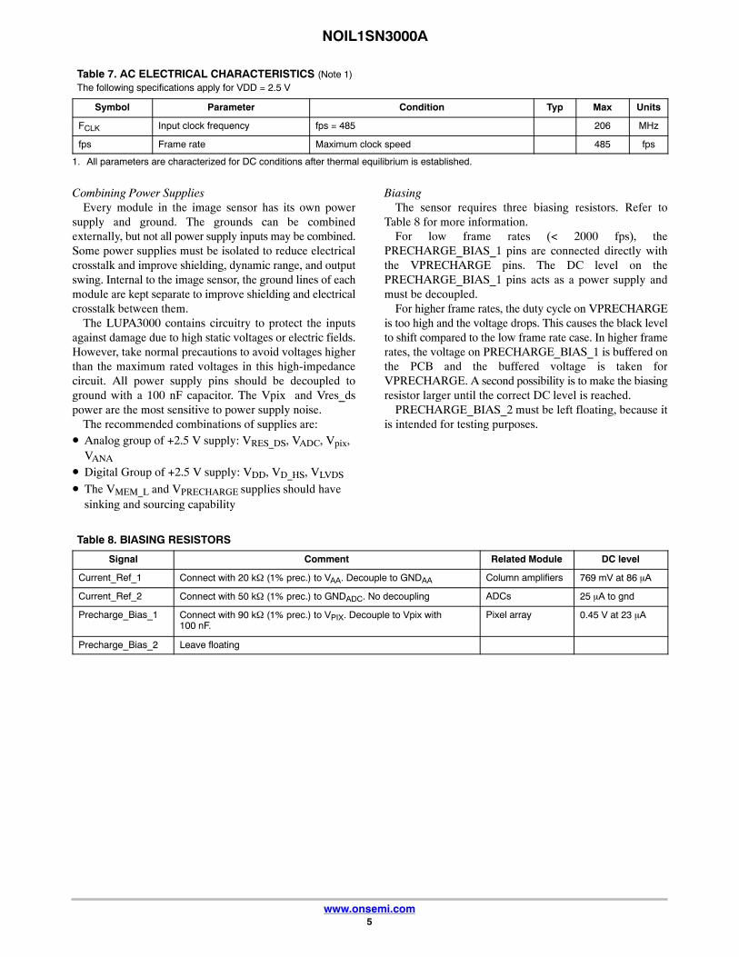
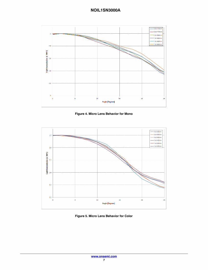
Spectral ResponseFigure 3 shows the spectral response of the mono and color versions of the LUPA3000. Figure 4 and Figure 5 on page 7 depict
the micro lens behaviour for mono and color devices for mid range wavelengths.
Figure 3. Mono and Color Spectral Response
NOIL1SN3000A
www.onsemi.com7
Figure 4. Micro Lens Behavior for Mono
Figure 5. Micro Lens Behavior for Color

NOIL1SN3000A
www.onsemi.com8
SENSOR ARCHITECTURE
Image Sensor CoreThe LUPA3000 floor plan is shown in Figure 6. The
sensor consists of the pixel array, column amplifiers, analogfront end (AFE) consisting of programmable gain amplifierand ADCs, data block (not shown), sequencer, and LVDStransmitter and receivers. The image sensor of 1696 x 1710active pixels is read out in progressive scan.
The architecture enables programmable addressing in thex-direction in steps of 32 pixels, and in the y-direction in
steps of one line. The starting point of the address can beuploaded by the SPI.
The AFE prepares the signal for the digital data blockwhen the data is multiplexed and prepared for the LVDSinterface.
NOTE: In Figure 7 on page 9, 32 pixels (1 kernel) areread out, where the most significant bit (MSB) isthe first bit out.
On chip drivers
Y-s
hift
regis
ter
Column amplifiers
X-shift register
64 ADC's
32 +2 LVDS drivers
Sequencer
Y
-shift
regis
ter
Pixel kernels 32 x 1
32
32
Odd kernels
Even kernels
Pixel (0,0)
Figure 6. Sensor Floor Plan
Pixel array1696 * 1710
NOIL1SN3000A
www.onsemi.com9
Figure 7. Column Multiplexing Scheme
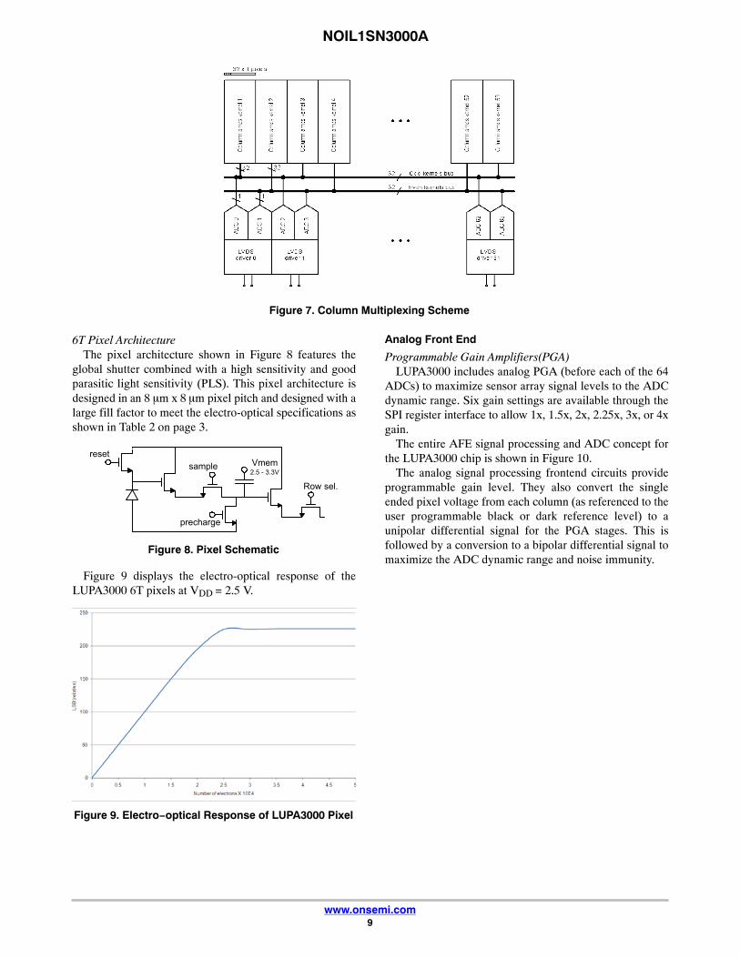
6T Pixel ArchitectureThe pixel architecture shown in Figure 8 features the
global shutter combined with a high sensitivity and goodparasitic light sensitivity (PLS). This pixel architecture isdesigned in an 8 m x 8 m pixel pitch and designed with alarge fill factor to meet the electro-optical specifications asshown in Table 2 on page 3.
Figure 8. Pixel Schematic
reset
sample Vmem2.5 - 3.3V
precharge
Row sel.
Figure 9 displays the electro-optical response of theLUPA3000 6T pixels at VDD = 2.5 V.
Figure 9. Electro−optical Response of LUPA3000 Pixel
Analog Front End
Programmable Gain Amplifiers(PGA)LUPA3000 includes analog PGA (before each of the 64
ADCs) to maximize sensor array signal levels to the ADCdynamic range. Six gain settings are available through theSPI register interface to allow 1x, 1.5x, 2x, 2.25x, 3x, or 4xgain.
The entire AFE signal processing and ADC concept forthe LUPA3000 chip is shown in Figure 10.
The analog signal processing frontend circuits provideprogrammable gain level. They also convert the singleended pixel voltage from each column (as referenced to theuser programmable black or dark reference level) to aunipolar differential signal for the PGA stages. This isfollowed by a conversion to a bipolar differential signal tomaximize the ADC dynamic range and noise immunity.

NOIL1SN3000A
www.onsemi.com10
Figure 10. Analog Frontend and ADC Concept
Table 9. PROGRAMMABLE AMPLIFIERS GAIN SETTINGS
Register Address d73 Gain Level Comments
Bit 2 Bit 1 Bit 0
0 0 0 1x POR default value
0 0 1 1.5x
0 1 0 2.0x
0 1 1 2.25x
1 0 0 3.0x
1 0 1 4.0x
1 1 x 3.0x Do not use (Redundant gain codes)
The gain is set through bits 2:0 in register 73 (decimal).The gain register controls the gain setting globally for all
64 PGA and ADC channels.A latency (delay) is incurred for the analog signal
processing, PGA, and ADC stages. The total latency is 44high-speed input clock delays. The output synchronizationsignals from the LVDS sync channel factor in this latency.
Programmable Dark LevelAn SPI-controlled DAC provides the PGA with a dark
level. This analog voltage corresponds with the all-zerooutput of the ADC. This dark level is tuned to optimally usethe ADC range.
The dark level coming from the pixels follow a Gaussiandistribution. This distribution is visible in a dark image asthe FPN. The spread on the distribution is influenced by thedark current and temperature. Typically the spread is100 mV peak-to-peak.
The average dark level of this distribution depends onseveral parameters:• The processing corner
• Tolerances on the pixel power supplies (Vpix, Vreset,Vmem_l, and Vmem_h)
• Pixel timingThe combination of these parameters adds an offset to the
dark level. The offset is in the order of magnitude of 200 mV.
To allow off-chip FPN calibration, the full spread on thedark level is mapped inside the range of the ADC. Tooptimally use the input range of the ADC, the spread on thedark level is mapped as close as possible to the high level ofthe ADC’s input range.
The default startup value of the dark level coming from theDAC is 1.5 V. This ensures that the spread on the dark levelis completely mapped in the ADC range. The startup DACdark level is not optimal. By taking a dark image afterstartup, the offset on the dark image histogram is measured.The offset from the optimal case is subtracted from the darklevel coming from the DAC. This places the dark leveldistribution optimally inside the range of the ADC. Followthis procedure after every change in operation conditionsuch as temperature, FOT timing, and ROT.
Analog- to-Digital ConvertersLUPA3000 includes 64 pipelined 9-bit ADCs operating at
approximately 25.75 mega samples per second (MSPS).Two ADCs are combined to provide digitized data to one ofthe 32 LVDS serialization channels. One of the ADC pairconverts data from an ‘odd kernel’ of the LUPA3000 pixelarray, the other from an ‘even kernel’. LUPA3000 onlyprocesses the eight MSBs of the converter to realize animproved noise performance 8-bit converter.

NOIL1SN3000A
www.onsemi.com11
The ADCs are designed using fully differential circuits toimprove performance and noise immunity. In addition, aredundant signed digit (RSD) 1.5 bit per stage architecturewith digital error correction is used to improve differentialnonlinearity (DNL) and ensure that no codes are missing.Interstage ADC gain errors are addressed usingcommutation techniques for capacitor matching.Auto-zeroing and other calibration methods areimplemented to remove offsets.
References and Programmable TrimmingBits 6:4 of SPI register 64 (decimal) allow adjustment of
the Vrefp-Vrefm differential ADC reference level. Eightsettings are provided to enable trimming of the dynamicrange. Reduced dynamic range is used to optimize signals inlow light intensity, where reduced pixel levels requirefurther gain. Table 10 provides the permitted trim settings.
Table 10. PROGRAMMABLE ADC REFERENCELEVEL
Register Address 64(dec)
Bit 6 Bit 5 Bit 4
Vrefp-Vrefm
Gain Level(typ)
Comments
0 0 0 0.5x Maximum effectivegain +6.0 dB (2x)
0 0 1 0.67x
0 1 0 0.71x
0 1 1 0.77x
1 0 0 0.83x
1 0 1 0.91x Available setting toensure 0 code
1 1 0 0.95x Available setting toensure 0 code
1 1 1 1.0 x POR (startup)default level
The black voltage level from the pixel array is morepositive than the user set Vdark or “black” reference level.This results in a nonzero differential voltage in the PGAs andother AFE stages. This condition prevents obtaining adesired 0 code out of the ADCs. The 0.95x and 0.91x trimsettings are specifically supplied to allow minor adjustmentto the ADC differential reference (Vrefp-Vrefm) to ensure azero level code in these conditions.
The additional trim settings are provided as dynamicrange adjustments in low light intensities to act as effectiveglobal gain settings. The absolute level of gain (from thetypical values) is not guaranteed. However, the gainincreases are monotonic. Using this method, you can obtaina maximum gain of approximately 2x (+6.0 dB). As a result,the combined gain of both PGAs and the ADC referencetrimming available is 8x maximum.
Some reference voltages are overdriven after the on-chipcontrol logic is powered down (refer section On−ChipBandGap Reference and Current Biasing on page 17).Overdriving, a feature intended for testing and debugging,is not recommended for normal operation. The referencevoltages that are overdriven are:• Vrefp - Vrefm (can be overdriven as a pair)
• Vcm
• Vdark
• Internal bandgap voltageTable 11 summarizes the ADC and AFE (signal
processing) parameters.Each pair of odd and even kernel AFE + ADC channels are
individually powered down with its associated LVDSserialization channel. This is controlled through bits in SPIregisters 66–70 (decimal). Logic 1 is the power down state.The POR defaults are logic 0 for all channels powered on.
Table 11. AFE AND ADC PARAMETERS
Parameter Parameter Value (typical) Comment
Input range (single to differential converter; S2D)
1.5 V to 0.3 V(SE to unipolar differential)
S2D performs inversion. Referenced from Vblack
Vblack 1.2 V to 1.5 V (typical) Dark or black level reference from SPI programmableDAC. 0.01 F to gnd
Analog PGA gain and settings 1x to 4x (6 gain settings) 3-bit SPI programmable. 1x, 1.5x, 2x, 2.25x, 3x, 4x
Input range (ADC) 0.75 V to 1.75 V 1 V maximum Vrefp-Vrefm (2 Vp-p maximum)
ADC type Pipelined (four ADC clock latency) With digital error correction (no missing codes)
ADC resolution 8 bits
Sampling rate per ADC 26.5 MSPS Maximum 30 MSPS
ENOB 7.5 bits Effective number of bits
Differential nonlinearity (DNL) ±0.5 LSB No missing codes
Integral nonlinearity (INL) ±1.0 LSB
Power supply 2.5 V ±0.25 V

NOIL1SN3000A
www.onsemi.com12
Table 11. AFE AND ADC PARAMETERS
Parameter CommentParameter Value (typical)
Total AFE + ADC latency 44 master clocks 5.5 ADC clocks = 1/8 of master clk
Total AFE + ADC power(32 channels = 64 AFE + ADC)
400 mW (at 2.5 V) 160 mA
Protocol LayerDigital data from the ADCs is reorganized in the protocol
layer before it is transferred to the LVDS drivers. Performthese operations in the protocol layer:• Multiplexing of two ADCs to one output data channel.
• Adding the cyclical redundancy check (CRC)checksum to the data stream. This operation is donerow by row. A new CRC checksum is calculated forevery new row that is readout.
• Switching readout mode. The LUPA3000 sensor isprogrammed to operate in two other readout modes:training and test image modes. These modessynchronize the readout circuitry of the end user withthe sensor.
• Assembling the data stream of the synchronizationchannel.
CRCLUPA3000 implements a CRC for each row (line) of
processed data to detect errors during the high speedtransmission. CRC provides error detection capability atlow cost and overhead.
The CRC polynomial implemented for LUPA3000 is:x^8+x^6+x^3+x^2+1.
The CRC result is transmitted with the original data.When the data is received (or recovered), the CRC algorithmis reapplied and the latest result compared to the originalresult. If a transmission error occurs, a different CRC resultis obtained. The system then chooses to operate on thedetected error or has the frame resent.
The CRC shift register is initialized with logic 1s at resetto improve bit error detection efficiency.
Referring to Figure 11, the CRC value is calculated foreach row and inserted into the serial data stream. Bit 0 of SPIregister 71 (decimal) is an enable bit to insert the CRCchecksum. CRC is enabled when a logic 1 is written to thisbit. This is the default (POR) value. Bit 1 of this registerallows calculation and insertion of a CRC checksum to the“synchronization” channel. No checksum is attached bydefault.
Figure 11. Equivalent Polynomial Representation in Serial Format
x0 x1 x2 x3 x4 x5 x6 x7
lsb msb
x8 + x6 + x3 + x2 + 1
datain
(msb first)

NOIL1SN3000A
www.onsemi.com13
Data BlockThe data block is positioned in between the AFE (output
stage + ADCs) and the LVDS interface. It multiplexes theoutputs of two ADCs to one LVDS block and performs someminor data handling:• Calculate and insert CRC
• Generate training and test pattern
It also contains a huge part of the functionality for blacklevel calibration.
A number of data blocks are placed in parallel to serve alldata output channels. One additional channel generates thesynchronization protocol. A high level overview isillustrated in Figure 12.
Figure 12. Interaction of the Data Block with ADC and LVDS
LVDSLUPA3000 uses LVDS I/O. LVDS offers low power and
low noise coupling. It also offers low EMI emissions that areessential for the high data readout rates that are required bythe LUPA3000 image sensor. LVDS voltage swings rangefrom 250 mV to 450 mV with a typical of 350 mV. Becauseof the low voltage swings, rise and fall times are reduced,enabling higher operating speeds than CMOS, TTL, or otherdrivers operating at the same slew rate. It uses a commonmode voltage ~1.2 V to 1.25 V above ground, and as a resultis more independent of the power supply level and lesssusceptible to noise. Differential transmission also reducesEMI levels. The 2-pin differential output drives a cable withapproximately 100 characteristic impedance, which is‘far-end’ terminated with 100 .
LVDS Data ChannelsLUPA3000 has 32 LVDS data output channels operating
at a double data rate (DDR) of 412 Mb per second (typical)using a 206-MHz input clock. The LVDS data channels havea high speed parallel to the serial converter logic function(serializer) that serializes the 52 MSPS 8-bit parallel datafrom a time multiplexed odd and even kernel ADC pair. Thehigh-speed serial bit stream drives a LVDS output driver.
The LVDS driver must deliver positive or negative currentthrough a 2-pin differential output to represent a logical 1and logical 0 state respectively. The driver is designed incompliance with the ANSI/TIA/EIA-644-A-2001 standard.The circuit consists of a programmable current sink thatdefines the drive current, a dynamically controlled currentsource, a 4-transistor bridge that steers these currents to thedifferential outputs, and a common mode feedback circuit tobalance the sink and source currents.
The LVDS standard defines the drive current between2.5 mA to 4.5 mA. The termination resistance is specifiedfrom 90 to 132 . To allow flexibility in powerconsumption, the output drive current is programmedthrough the SPI register interface. Settings are available foroperation outside the specified ANSI standard to allowcustom settings for power and speed enhancements. Thesesettings may require the use of nonstandard terminationresistance. Current drive programming is accomplishedusing bits 3:0 of SPI register 72 (decimal – LVDS trim).Figure 13 on page 14 defines the programmable LVDSoutput current settings.

NOIL1SN3000A
www.onsemi.com14
Figure 13. LVDS Driver Programmable Drive Current Settings
378
357
336
315
404
347
337
420
375
336
294
252
378
168
126
V
210
Interconnect capacitance
OUT [mV]
Extra drive current
Standard range
Low power range
to accommodate high
507.561111
507.141110
506.721101
506.31100
68.755.881011
Comments
68.755.46
68.755.041001
72.974.621000
1004.20111
1010
1003.78
1003.360101
1002.940100
1002.520011
0110
1002.1
1001.680001
1001.260000
0010
RT[Ω]IOUT [mA]REG 72 < 3:0>
LVDS Sync ChannelLUPA3000 includes a LVDS output channel to encode
sensor synchronization control words such as start of frame(SOF), start of line (SOL), end of line (EOL), idle words(IdleA and IdleB), and the sensor line address.
This channel includes a serializer logic section, butreceives its input directly from the image core sequencer. Anadditional synchronization control logic block ensuresproper data alignment of the synchronization codes toaccount for the latency incurred in the other 32 data channels(due to AFE and ADC signal processing). The LVDS outputdriver is similar to that used in other data channel outputs.
LVDS Clk (Clock) OutputThe LUPA3000 provides a LVDS clock output channel.
This channel provides an output clock that is in phase andaligned with the data bit stream of the 32 data channels. It isrequired for clock and data recovery by the systemprocessing circuits.
A serializer logic section is connected to accept thedifferential CMOS serializer clock, after processing throughthe clock distribution buffer network that provides clocks toall LUPA3000 data channels. The group delay of the outputclock and data channels is ~2.5 ns relative to the incomingmaster clock. The LVDS output driver is similar to that usedin other data channel outputs.
LVDS CLK (Clock) InputLUPA3000 includes a differential LVDS receiver for the
master input clock. The input clock rate is typically206 MHz and also complies with the ANSI LVDS receiverstandards. The input clock drives the internal clockgenerator circuit that produces the required internal clocksfor image core and sequencer, AFE and ADCs, CRCinsertion logic, and serializers. LUPA3000 requires the
following internal clock domains (all internal clock domainsare 2.5 V CMOS levels):• Serializer clock = 1x differential version of the input
clock (206 MHz typical)• CRC clock = 1/4x the input clock (51.5 MHz typical)
• Load pulse = 1/4 (the input clock)at 12.5% duty cycleversion of the input clock: for load and handshakebetween CRC parallel data to serializer
• ADC and AFE clock = 1/8x the input clock(25.75 MHz typical)
• Sensor clock = 1/4x the input clock (51.5 MHz typical)with programmable delay
• ADC clock =1/8x the input clock (25.75 MHz typical)with programmable delayAll clock domains are designed with identical clock buffer
networks to ensure equal group delays and maintain lessthan 100 ps maximum channel to channel clock variation.
Programmable delay adjustment is provided for the clockdomains of image sensor core and sequencer. Thisadjustment optimizes the data acquisition handshakingbetween the image sensor core and the digitization andserialization channels. SPI register 65 (decimal) controlsdelay (or advance) adjustments for these two clocks. Foreach of these two imager clocks, 15 adjustments settings areprovided. Each setting allows adjustment for 1/(2x masterclock) adjustment. For example, if the master input clockruns at 206 MHz, 1/412 MHz = 2.41 ns adjustmentresolution is possible. Refer to Sensor Clock Edge AdjustRegister (b1000001 / d65) on page 26 for programmingdetails.
ON Semiconductor provides default settings for theprogrammable delay. These settings allow correct
NOIL1SN3000A
www.onsemi.com15
operation; there is no need to change these settings (unlessfor testing).
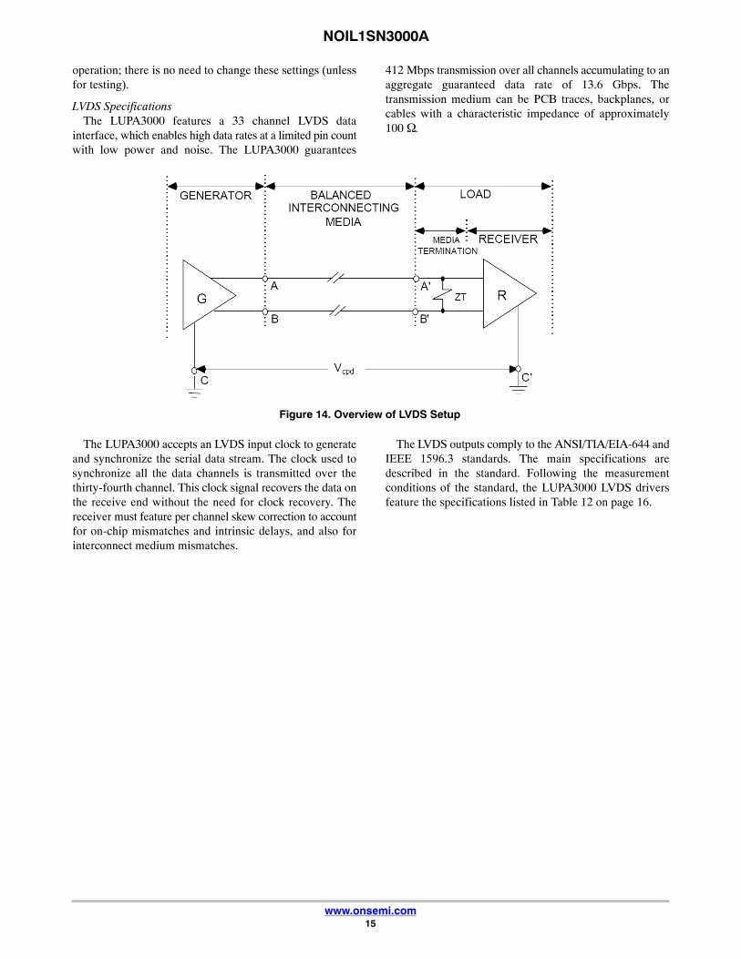
LVDS SpecificationsThe LUPA3000 features a 33 channel LVDS data
interface, which enables high data rates at a limited pin countwith low power and noise. The LUPA3000 guarantees
412 Mbps transmission over all channels accumulating to anaggregate guaranteed data rate of 13.6 Gbps. Thetransmission medium can be PCB traces, backplanes, orcables with a characteristic impedance of approximately100 .
Figure 14. Overview of LVDS Setup
The LUPA3000 accepts an LVDS input clock to generateand synchronize the serial data stream. The clock used tosynchronize all the data channels is transmitted over thethirty-fourth channel. This clock signal recovers the data onthe receive end without the need for clock recovery. Thereceiver must feature per channel skew correction to accountfor on-chip mismatches and intrinsic delays, and also forinterconnect medium mismatches.
The LVDS outputs comply to the ANSI/TIA/EIA-644 andIEEE 1596.3 standards. The main specifications aredescribed in the standard. Following the measurementconditions of the standard, the LUPA3000 LVDS driversfeature the specifications listed in Table 12 on page 16.
NOIL1SN3000A
www.onsemi.com16
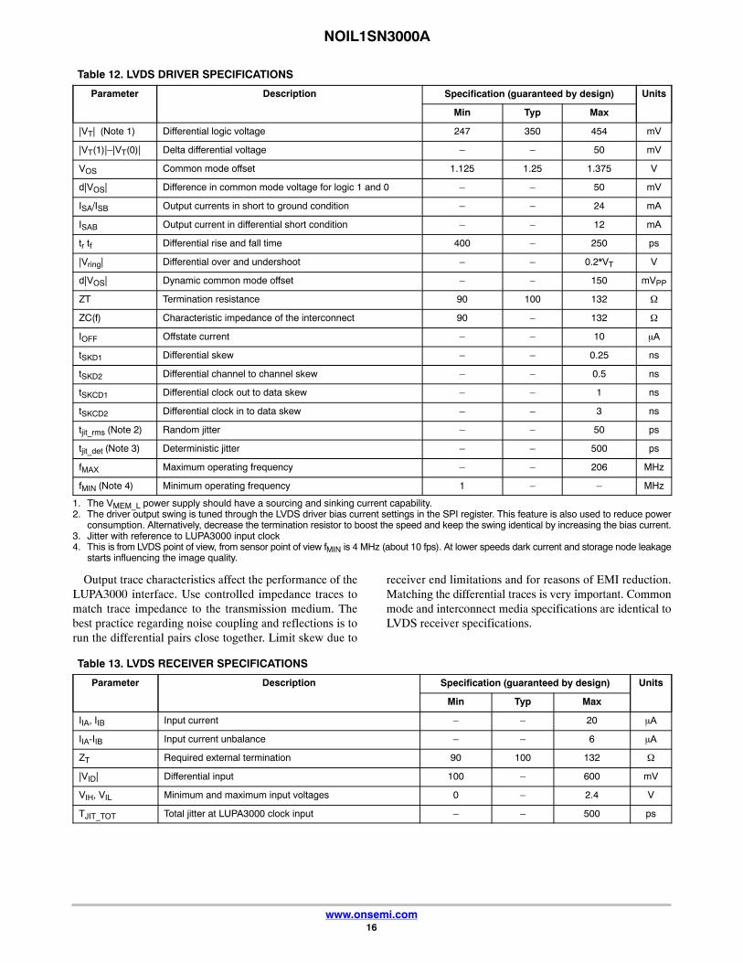
Table 12. LVDS DRIVER SPECIFICATIONS
Parameter Description Specification (guaranteed by design) Units
Min Typ Max
|VT| (Note 1) Differential logic voltage 247 350 454 mV
|VT(1)|–|VT(0)| Delta differential voltage – – 50 mV
VOS Common mode offset 1.125 1.25 1.375 V
d|VOS| Difference in common mode voltage for logic 1 and 0 – – 50 mV
ISA/ISB Output currents in short to ground condition – – 24 mA
ISAB Output current in differential short condition – – 12 mA
tr tf Differential rise and fall time 400 – 250 ps
|Vring| Differential over and undershoot – – 0.2*VT V
d|VOS| Dynamic common mode offset – – 150 mVPP
ZT Termination resistance 90 100 132
ZC(f) Characteristic impedance of the interconnect 90 – 132
IOFF Offstate current – – 10 A
tSKD1 Differential skew – – 0.25 ns
tSKD2 Differential channel to channel skew – – 0.5 ns
tSKCD1 Differential clock out to data skew – – 1 ns
tSKCD2 Differential clock in to data skew – – 3 ns
tjit_rms (Note 2) Random jitter – – 50 ps
tjit_det (Note 3) Deterministic jitter – – 500 ps
fMAX Maximum operating frequency – – 206 MHz
fMIN (Note 4) Minimum operating frequency 1 – – MHz
1. The VMEM_L power supply should have a sourcing and sinking current capability.2. The driver output swing is tuned through the LVDS driver bias current settings in the SPI register. This feature is also used to reduce power
consumption. Alternatively, decrease the termination resistor to boost the speed and keep the swing identical by increasing the bias current.3. Jitter with reference to LUPA3000 input clock4. This is from LVDS point of view, from sensor point of view fMIN is 4 MHz (about 10 fps). At lower speeds dark current and storage node leakage
starts influencing the image quality.
Output trace characteristics affect the performance of theLUPA3000 interface. Use controlled impedance traces tomatch trace impedance to the transmission medium. Thebest practice regarding noise coupling and reflections is torun the differential pairs close together. Limit skew due to
receiver end limitations and for reasons of EMI reduction.Matching the differential traces is very important. Commonmode and interconnect media specifications are identical toLVDS receiver specifications.
Table 13. LVDS RECEIVER SPECIFICATIONS
Parameter Description Specification (guaranteed by design) Units
Min Typ Max
IIA, IIB Input current – – 20 A
IIA-IIB Input current unbalance – – 6 A
ZT Required external termination 90 100 132
|VID| Differential input 100 – 600 mV
VIH, VIL Minimum and maximum input voltages 0 – 2.4 V
TJIT_TOT Total jitter at LUPA3000 clock input – – 500 ps

NOIL1SN3000A
www.onsemi.com17
On−Chip BandGap Reference and Current BiasingFor current biasing and voltage reference requirements
for the AFEs, ADCs, and LVDS I/O, LUPA3000 includes abandgap voltage reference that is typically 1.25 V. Thisreference is used to generate the differential Vrefp–VrefmADC reference and a analog voltage reference for the LVDSdriver I/O.
The bandgap reference voltage also forms a stable currentreference for the LVDS drivers and bias currents for all of theanalog amplifiers. A Current-Ref_2 pin is included on thepackage to allow connection of an ~50 K resistor (±1%) tognd to realize a desired 25 A current sourced from theLUPA3000 device. A buffered version of the internalbandgap reference is monitored at this pin.
An optional mode is available to enable an externalbandgap regulator. Control bits in SPI register 74 (decimal)allow this feature. Bit 2 is a power-down control bit for theinternal bandgap. Setting this bit high along with bit 1(int_res), and bit 0 (bg_disable), allow driving theCurrent_Ref_2 pin with an external reference. An internalcurrent reference resistor of 50 K to ground is applied. Thismode has reduced current accuracy; ~±10% from theexternal resistor mode (±1%).
Five trimming levels for the internal bandgap voltage areavailable through bits 2:0 of SPI register 64 (decimal). This
allows minor adjustment in process variations for voltagelevel and temperature tracking. A POR value is preset so thatuser adjustment is not required. Each setting adjusts aninternal resistor value used to adjust the PTAT (proportionalto absolute temperature) “K” factor ratio. Each of the fivesettings affect the “K” trimming factor by ~1.2%. Minoradjustments are made to tune the reference voltage level andtemperature tracking rate to compensate for IC processingvariations.
The reference generation circuits also form the internalanalog common mode voltage for the differential analogcircuits. The Vcm level is available at a package pin forexternal decoupling and should be driven by a 0.9 V supply(refer to Table 44 on page 29). The Vdark or “black” levelreference supplied from an on-chip SPI programmable DACis also buffered and distributed on-chip as input to each ofthe 64 AFE and ADC channels. This signal is also availableat a package pin for external decoupling. Separate powerdown control bits are available for the differential ADCreference (Vrefp–Vrefm), Vcm, and Vdark. When any ofthese are powered down, external references are driven onthe external package pins. Table 14 overviews primaryparameters for the references and biases.
Table 14. REFERENCE AND BIAS PARAMETERS
Parameter Parameter Value (Typical) Comment
Vrefp 1.7 V to 1.75 V At VDD = 2.5 V. Requires 0.01 F to gnd.
Vrefm 0.8 V to 0.75 V At VDD = 2.5 V. Requires 0.01 F to gnd.
Vrefp–Vrefm 0.95 V to 1.0 V (difference) ADC range. 3-bit SPI trim settings 1x, 0.95x, 0.91x, 0.83x, 0.77x,0.71x, 0.67x, 0.5x.
Vcm 0.9 V External power supply voltage. Requires 10 nF to gnd.Refer to Table 44 on page 29.
Current_Ref_2 1.25 V ± 0.1 V at 25 A to gnd Must pull down to gnd with ~ 50 k.
Bandgap reference (internal) 1.25 V ± 0.05 V at 2.5 V, T = 40°C Typical < 50 PPM. Level and tracking are 3-bit SPI trimmable. Fivesettings at ~ 1.2% adjust per step.
NOIL1SN3000A
www.onsemi.com18
Sequencer and LogicThe sequencer generates the internal timing of the image
core based on the SPI settings uploaded. You can control thefollowing settings:• Window resolution• FOT and ROT• Enabling or disabling reduced ROT mode• Readout modes (training, test image, and normal)
Table 15. DETAILED DESCRIPTION OF SPI REGISTERS
Address Bits Name Description
0 <5:0> SEQUENCER
<0> Power down Power down analog core
<1> Reset_n_seq Reset_n of on chip sequencer
<2> Red_rot Enable reduced ROT mode
<3> Ds_en Enable DS operation
<5:4> Sel_pre_width Width of sel_pre pulse
1 <4:0> ROT_TIMER Length of ROT
2 <7:0> PRECHARGE_TIMER Length of pixel precharge in clk/4
3 <7:0> SAMPLE_TIMER Length of pixel sample in clk/4
4 <7:0> VMEM_TIMER Length of pixel vmem in clk/4
5 <7:0> FOT_TIMER Length of FOT in clk/4
6 <5:0> NB_OF_KERNELS Number of kernels to readout
7 <7:0> Y_START <7:0> Start pointer Y readout
8 <2:0> Y_START <10:8>
9 <7:0> Y_END <7:0> End pointer Y readout
10 <2:0> Y_END <10:8>
11 <4:0> X_START Start pointer X
12 <1:0> TRAINING
<0> Training_en 1: Transmit training pattern; 0: transmit test patterns
<1> Bypass_en 1: Evaluate TRAINING_EN bit; 0: ignore TRAINING_EN bit,captured image readout.
<2> Analog_out_en Enable analog output
13 <7:0> BLACK_REF ADC black reference
14 <6:0> BIAS_COL_LOAD Biasing of column load
15 <7:0> BIASING_CORE_1 Biasing of image core
<3:0> Bias_col_amp Biasing of first column amplifier
<7:4> Bias_col_outputamp Biasing of the output column amplifier
16 <7:0> BIASING_CORE_2 Biasing of image core
<3:0> Bias_sel_pre Biasing for column precharge structure
<7:4> Bias_analog_out Biasing for analog output amplifier
17 <7:0> BIASING_CORE_3 Biasing of image core
<3:0> Bias_decoder_y Biasing of y decoder
<7:4> Bias_decoder_x Biasing of x decoder
30 <7:0> FIXED Fixed, read only register
31 <7:0> CHIP_REV_NB Chip revision number
NOIL1SN3000A
www.onsemi.com19
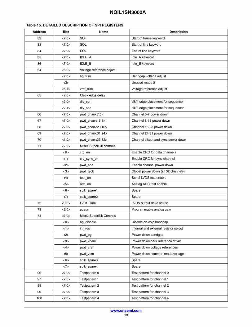
Table 15. DETAILED DESCRIPTION OF SPI REGISTERS
Address DescriptionNameBits
32 <7:0> SOF Start of frame keyword
33 <7:0> SOL Start of line keyword
34 <7:0> EOL End of line keyword
35 <7:0> IDLE_A Idle_A keyword
36 <7:0> IDLE_B Idle_B keyword
64 <6:0> Voltage reference adjust
<2:0> bg_trim Bandgap voltage adjust
<3> Unused reads 0
<6:4> vref_trim Voltage reference adjust
65 <7:0> Clock edge delay
<3:0> dly_sen clk/4 edge placement for sequencer
<7:4> dly_seq clk/8 edge placement for sequencer
66 <7:0> pwd_chan<7:0> Channel 0-7 power down
67 <7:0> pwd_chan<15:8> Channel 8-15 power down
68 <7:0> pwd_chan<23:16> Channel 16-23 power down
69 <7:0> pwd_chan<31:24> Channel 24-31 power down
70 <1:0> pwd_chan<33:32> Channel clkout and sync power down
71 <7:0> Misc1 SuperBlk controls
<0> crc_en Enable CRC for data channels
<1> crc_sync_en Enable CRC for sync channel
<2> pwd_ena Enable channel power down
<3> pwd_glob Global power down (all 32 channels)
<4> test_en Serial LVDS test enable
<5> atst_en Analog ADC test enable
<6> sblk_spare1 Spare
<7> sblk_spare2 Spare
72 <3:0> LVDS Trim LVDS output drive adjust
73 <2:0> pgagn Programmable analog gain
74 <7:0> Misc2 SuperBlk Controls
<0> bg_disable Disable on-chip bandgap
<1> int_res Internal and external resistor select
<2> pwd_bg Power down bandgap
<3> pwd_vdark Power down dark reference driver
<4> pwd_vref Power down voltage references
<5> pwd_vcm Power down common mode voltage
<6> sblk_spare3 Spare
<7> sblk_spare4 Spare
96 <7:0> Testpattern 0 Test pattern for channel 0
97 <7:0> Testpattern 1 Test pattern for channel 1
98 <7:0> Testpattern 2 Test pattern for channel 2
99 <7:0> Testpattern 3 Test pattern for channel 3
100 <7:0> Testpattern 4 Test pattern for channel 4
NOIL1SN3000A
www.onsemi.com20
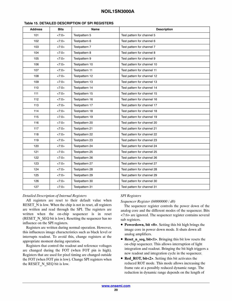
Table 15. DETAILED DESCRIPTION OF SPI REGISTERS
Address DescriptionNameBits
101 <7:0> Testpattern 5 Test pattern for channel 5
102 <7:0> Testpattern 6 Test pattern for channel 6
103 <7:0> Testpattern 7 Test pattern for channel 7
104 <7:0> Testpattern 8 Test pattern for channel 8
105 <7:0> Testpattern 9 Test pattern for channel 9
106 <7:0> Testpattern 10 Test pattern for channel 10
107 <7:0> Testpattern 11 Test pattern for channel 11
108 <7:0> Testpattern 12 Test pattern for channel 12
109 <7:0> Testpattern 13 Test pattern for channel 13
110 <7:0> Testpattern 14 Test pattern for channel 14
111 <7:0> Testpattern 15 Test pattern for channel 15
112 <7:0> Testpattern 16 Test pattern for channel 16
113 <7:0> Testpattern 17 Test pattern for channel 17
114 <7:0> Testpattern 18 Test pattern for channel 18
115 <7:0> Testpattern 19 Test pattern for channel 19
116 <7:0> Testpattern 20 Test pattern for channel 20
117 <7:0> Testpattern 21 Test pattern for channel 21
118 <7:0> Testpattern 22 Test pattern for channel 22
119 <7:0> Testpattern 23 Test pattern for channel 23
120 <7:0> Testpattern 24 Test pattern for channel 24
121 <7:0> Testpattern 25 Test pattern for channel 25
122 <7:0> Testpattern 26 Test pattern for channel 26
123 <7:0> Testpattern 27 Test pattern for channel 27
124 <7:0> Testpattern 28 Test pattern for channel 28
125 <7:0> Testpattern 29 Test pattern for channel 29
126 <7:0> Testpattern 30 Test pattern for channel 30
127 <7:0> Testpattern 31 Test pattern for channel 31
Detailed Description of Internal RegistersAll registers are reset to their default value when
RESET_N is low. When the chip is not in reset, all registersare written and read through the SPI. The registers arewritten when the on-chip sequencer is in reset(RESET_N_SEQ bit is low). Resetting the sequencer has noinfluence on the SPI registers.
Registers are written during normal operation. However,this influences image characteristics such as black level orinterrupts readout. To avoid this, change registers at theappropriate moment during operation.
Registers that control the readout and reference voltagesare changed during the FOT (when FOT pin is high).Registers that are used for pixel timing are changed outsidethe FOT (when FOT pin is low). Change SPI registers whenthe RESET_N_SEQ bit is low.
SPI Registers
Sequencer Register (b0000000 / d0)The sequencer register controls the power down of the
analog core and the different modes of the sequencer. Bits<7:6> are ignored. The sequencer register contains severalsub registers.• Powerdown, bit <0>. Setting this bit high brings the
image core in power down mode. It shuts down allanalog amplifiers.
• Reset_n_seq, bit<1>. Bringing this bit low resets theon-chip sequencer. This allows interruption of lightintegration and readout. Bringing the bit high triggers anew readout and integration cycle in the sequencer.
• Red_ROT, bit<2>. Setting this bit activates thereduced ROT mode. This mode allows increasing theframe rate at a possibly reduced dynamic range. Thereduction in dynamic range depends on the length of

NOIL1SN3000A
www.onsemi.com21
the ROT. See ROT_timer (b0000001 / d1) on page 21.The default timing is in reduced ROT mode, so there isno reduction in dynamic range.
• Ds_en, bit<3>. Bit to enable dual slope operation.Enabling this mode allows to enlarge optical dynamicrange.
• Sel_pre_width, bit<5:4>. Setting these two bits allowschanging the width of the sel_pre pulse that is used toprecharge all column lines at the start of every ROT.Changing these bits does not change the total ROTlength.
Table 16. SEQUENCER REGISTER
Value Effect
Powerdown, bit <0>
0 Normal operation
1 Image core in power down
On startup 0
Reset_n_seq, bit<1>
0 Sequencer kept in reset
1 Normal operation
On startup 1
Red_ROT, bit<2>
0 Long ROT mode
1 Reduced ROT mode
On startup 1
Ds_en, bit<3>
0 Disable dual slope operation
1 Enable dual slope operation
On startup 0
Sel_pre_width, bit<5:4>
00 Sel_pre is 1 sensor clock period long (4 master clocks)
01 Sel_pre is 2 sensor clock periods long (8 master clocks)
10 Sel_pre is 3 sensor clock periods long (12 master clocks)
11 Same effect as ‘10’ setting
On startup 00
ROT_timer (b0000001 / d1)The ROT_timer register controls the length of the ROT.
The ROT length, in number of sensor clock periods, isexpressed by the formula: ROT length = ROT_timer + 2.
The relation between the row overhead time and the ROTpin is described in the section ROT Pin on page 39. Bits<7:5> are ignored.
Table 17. ROT TIMER REGISTER
Value Bit<4:0> Effect
00000 ROT length is 35 sensor clocks, 140 master clocks.
xxxxx ROT length is <N+2> sensor clocks (<N+2>*4 master clocks) where N is the register value
On startup 00111 (9 sensor clocks)
NOIL1SN3000A
www.onsemi.com22
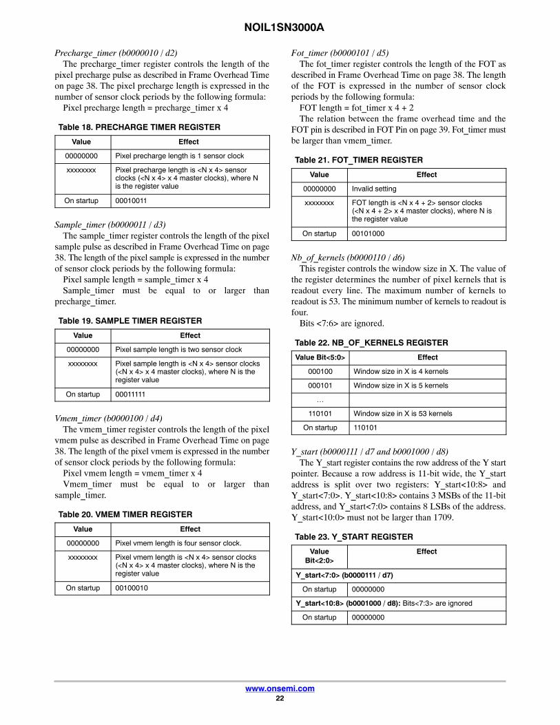
Precharge_timer (b0000010 / d2)The precharge_timer register controls the length of the
pixel precharge pulse as described in Frame Overhead Timeon page 38. The pixel precharge length is expressed in thenumber of sensor clock periods by the following formula:
Pixel precharge length = precharge_timer x 4
Table 18. PRECHARGE TIMER REGISTER
Value Effect
00000000 Pixel precharge length is 1 sensor clock
xxxxxxxx Pixel precharge length is <N x 4> sensorclocks (<N x 4> x 4 master clocks), where Nis the register value
On startup 00010011
Sample_timer (b0000011 / d3)The sample_timer register controls the length of the pixel
sample pulse as described in Frame Overhead Time on page38. The length of the pixel sample is expressed in the numberof sensor clock periods by the following formula:
Pixel sample length = sample_timer x 4Sample_timer must be equal to or larger than
precharge_timer.
Table 19. SAMPLE TIMER REGISTER
Value Effect
00000000 Pixel sample length is two sensor clock
xxxxxxxx Pixel sample length is <N x 4> sensor clocks (<N x 4> x 4 master clocks), where N is theregister value
On startup 00011111
Vmem_timer (b0000100 / d4)The vmem_timer register controls the length of the pixel
vmem pulse as described in Frame Overhead Time on page38. The length of the pixel vmem is expressed in the numberof sensor clock periods by the following formula:
Pixel vmem length = vmem_timer x 4Vmem_timer must be equal to or larger than
sample_timer.
Table 20. VMEM TIMER REGISTER
Value Effect
00000000 Pixel vmem length is four sensor clock.
xxxxxxxx Pixel vmem length is <N x 4> sensor clocks (<N x 4> x 4 master clocks), where N is theregister value
On startup 00100010
Fot_timer (b0000101 / d5)The fot_timer register controls the length of the FOT as
described in Frame Overhead Time on page 38. The lengthof the FOT is expressed in the number of sensor clockperiods by the following formula:
FOT length = fot_timer x 4 + 2The relation between the frame overhead time and the
FOT pin is described in FOT Pin on page 39. Fot_timer mustbe larger than vmem_timer.
Table 21. FOT_TIMER REGISTER
Value Effect
00000000 Invalid setting
xxxxxxxx FOT length is <N x 4 + 2> sensor clocks (<N x 4 + 2> x 4 master clocks), where N isthe register value
On startup 00101000
Nb_of_kernels (b0000110 / d6)This register controls the window size in X. The value of
the register determines the number of pixel kernels that isreadout every line. The maximum number of kernels toreadout is 53. The minimum number of kernels to readout isfour.
Bits <7:6> are ignored.
Table 22. NB_OF_KERNELS REGISTER
Value Bit<5:0> Effect
000100 Window size in X is 4 kernels
000101 Window size in X is 5 kernels
…
110101 Window size in X is 53 kernels
On startup 110101
Y_start (b0000111 / d7 and b0001000 / d8)The Y_start register contains the row address of the Y start
pointer. Because a row address is 11-bit wide, the Y_startaddress is split over two registers: Y_start<10:8> andY_start<7:0>. Y_start<10:8> contains 3 MSBs of the 11-bitaddress, and Y_start<7:0> contains 8 LSBs of the address.Y_start<10:0> must not be larger than 1709.
Table 23. Y_START REGISTER
ValueBit<2:0>
Effect
Y_start<7:0> (b0000111 / d7)
On startup 00000000
Y_start<10:8> (b0001000 / d8): Bits<7:3> are ignored
On startup 00000000

NOIL1SN3000A
www.onsemi.com23
Y_end (b0001001 / d9 and b0001010 / d10)The Y_end register contains the row address of the last
row to readout. Because a row address is 11-bit wide, theY_end address is split over two registers: Y_end<10:8> andY_end<7:0>. Y_end<10:8> contains 3 MSBs of the 11-bitaddress, and Y_end<7:0> contains 8 LSBs of the address.Y_end<10:0> must be larger than Y_start<10:0> and notlarger than 1709.
Table 24. Y_END REGISTER
ValueBit<2:0>
Effect
Y_end<7:0> (b0001001 / d9)
On startup 10101101
Y_end<10:8> (b0001010 / d10): Bits<7:3> are ignored
On startup 00000110
X_start (b0001011 / d11)The X_start register contains the start position for the X
readout. Readout in X starts only at odd kernel positions. Asa result, possible start positions are 64 columns (2 kernels)separated from each other.
Bits <7:5> are ignored.
Table 25. X_START REGISTER
ValueBit<4:0>
Effect
00000 X readout starts with the first kernel (column 0)
00001 X readout starts with the third kernel(column 64)
11010 X readout starts with the fifty third kernel(column 1664)
On startup 00000
Training (b0001100 / d12)This register allows switching between different readout
modes. Bits <7:2> are ignored.• Training_en, bit<0>. In bypass mode, this bit is
evaluated and determines if the training pattern or testimage is transmitted.
• Bypass_mode, bit<1>. This bit allows the sensor toswitch between normal readout of an image and readoutfor testing or training purposes.
• Analog_out_en, bit<2>.This bit activates the analogoutput of the sensor. The analog value ofcolumn<1696> is brought to the output.
Table 26. TRAINING REGISTER
Value Effect
Training_en, bit<0>
1 In bypass mode, the training pattern istransmitted
0 In bypass mode, the test image is transmitted
On startup 0
Bypass_mode, bit<1>
0 Normal readout of captured images
1 Bypass mode readout. The content of registerTRAINING_EN is evaluated.
On startup 0
Analog_out_en, bit<2>
0 Analog output disabled
1 Analog output enabled
On startup 0
Black_ref (b0001101 / d13)This register controls the DAC that sets the dark level for
the ADC. The analog output of the DAC corresponds withthe all zero code of the ADC. The DAC has an 8-bitresolution and outputs between VAA2V5 and 0 V. Thismeans that the step size corresponds with about 9.8 mV. TheDAC itself outputs between VAA2V5 and 0 V, but thebuffering circuit that follows after the DAC clips the voltageclose to ground and supply.
Table 27. BLACK_REF REGISTER
Value Effect
00000000 Output of DAC is VAA2V5
00000001 Output of DAC is VAA2V5–9.8 mV
…
11111111 Output of DAC is 0 V
On startup 01100110

NOIL1SN3000A
www.onsemi.com24
Bias_col_load (b0001110 / d14)This register controls the biasing current of the column
load. A higher biasing current has the following effects:• Faster settling on the pixel columns
• Increased power consumption from Vpix.
• Lower dark levelBias current changes 1.56 A per LSB. Bits <7:6> are
ignored.
Table 28. BIAS_COL_LOAD REGISTER
Value(Bit<5:0>)
Effect
000000 Bias current is 0 A
…
111111 Maximum bias current
On startup 001000 (13.6 A)
Biasing_1 (b0001111 / d15)• Bias_col_amp, bits<3:0>. This register controls the
biasing current of the first column amplifier. Theregister value must not be changed.
• Bias_col_outputamp, bits<7:4>. This register controlsthe biasing current of the output column amplifier. Theregister value must not be changed.
Table 29. BIASING_1 REGISTER
Value Effect
Bias_col_amp, bits<3:0>
0000 Bias current is 0 A
…
1111 Maximum bias current
On startup 0111 (0.4 A)
Bias_col_outputamp, bits<7:4>
0000 Bias current is 0 A
…
1111 Maximum bias current
On startup 0111 (6.5 A)
Biasing_2 (b0010000 / d16)• Bias_sel_pre, bits<3:0>. This register controls the
biasing current of the column precharge structure. Theregister value must not be changed. Bias currentchanges 57 A per LSB.
• Bias_analog_out, bits<7:4>. This register controls thebiasing current of the last stage of the analog amplifier.The register value must not be changed.
Table 30. BIASING_2 REGISTER
Value Effect
Bias_sel_pre, bits<3:0>
0000 Bias current is 0 A
…
1111 Maximum bias current
On startup 0111 (~ 500 A)
Bias_analog_out, bits<7:4>
0000 Bias current is 0 A
…
1111 Maximum bias current
On startup 0111
Biasing_3 (b0010001 / d17)• Bias_decoder_y, bits<3:0>. This register controls the
biasing current of the y decoder. The register valuemust not be changed.
• Bias_decoder_x, bits<7:4>. This register controls thebiasing current of the last stage of the analog amplifier.The register value must not be changed.
Table 31. BIASING_3 REGISTER
Value Effect
Bias_decoder_y, bits<3:0>
0000 Bias current is 0 A
…
1111 Maximum bias current
On startup 0111
Bias_decoder_x, bits<7:4>
0000 Bias current is 0 A
…
1111 Maximum bias current
On startup 0111
NOIL1SN3000A
www.onsemi.com25
Fixed (b0011110 / d30)This register is read only and always returns 11000100.
Table 32. FIXED REGISTER
Value Effect
On startup 11000100
Chip_rev_nb (b0011111 / d31)This register contains the revision number of the chip. It
is a read only register and a write operation does not have anyeffect.
The revision number is not guaranteed to represent allmask changes. Some mask changes do not allow to changethe revision number.
Table 33. CHIP_REV_NB REGISTER
Value Effect
00000001 Rev. A
00000010 Rev. B
…
On startup Current revision number
SOF (b0100000 / d32)This register contains the SOF keyword.
Table 34. SOF REGISTER
Value Effect
On startup 00100000
SOL (b0100001 / d33)This register contains the SOL keyword.
Table 35. SOL REGISTER
Value Effect
On startup 00100010
EOL (b0100010 / d34)This register contains the EOL keyword.
Table 36. EOL REGISTER
Value Effect
On startup 00100011
Idle_A (b0100011 / d35)This register contains the idle A keyword.
Table 37. IDLE_A REGISTER
Value Effect
On startup 11101011
Idle_B (b0100100 / d36)This register contains the idle B keyword.
Table 38. IDLE_B REGISTER
Value Effect
On startup 11101011
Reference Voltage Adjust Register (b1000000 / d64)The reference voltage adjust register allows trimming of
the bandgap and vref levels. Bits <7> and <3> are ignored.• bg_trim, bits <2:0>: Setting these bits adjusts the
bandgap voltage by selecting the value for the on-chipresistor R2. This resistor trims the PTAT “K” factor.See On−Chip BandGap Reference and Current Biasingon page 17
• vref_trim, bits <6:4>: Setting these bits adjusts thereference voltage range (vrefp-vrefm) for the ADCs.
Table 39. REFERENCE VOLTAGE ADJUSTREGISTER
Value Effect
bg_trim, bits <2:0>
000 R2= 82.5K
001 R2= 83.5K
010 R2= 84.5K Vbg 1.25 Vnominal
011 R2= 85.5K
1xx R2= 86.5K
On startup 010
vref_trim, bits <6:4>
000 0.50x
001 0.67x
010 0.71x
011 0.77x
100 0.83x
101 0.91x
110 0.95x
111 1.00x nominal
On startup 111

NOIL1SN3000A
www.onsemi.com26
Sensor Clock Edge Adjust Register (b1000001 / d65)The sensor clock edge adjust register allows
programmable delay between the column readout and theADC capture clock edges. The relationship is programmedto align to ±7 edges of the input high-speed clock (input lvds
clock or CLK_SER). Figure 15 shows this relationshipbetween the input clock and all the derived on-chip clocks.Some examples of programmed delay values for bothCLK_SEN and CLK_SEQ are also shown.
Figure 15. LUPA3000 Internal Clocking
7 6 5 4 3 2 1 0 7 6 5 4 3 21 0
ADC_OUT
CRC_OUT
CLK_ADC
DAT A( N )
DAT A (N +1 )
DA TA (N + 1 )7 6 5 4 3 2 1 0
CLK_SEN
DLY_SEN = 0000
0001
0010
0011
0100
0101
0110
0111
1000
1001
1010
1011
1100
1101
1110
1111
DATA(N−1)
DAT A( N )
DA TA (N + 1 )
CLK_SEQ
0000
0001
DLY_SE Q =
1111
0111
CLK_CRC
CLK_SER
SER_LOAD
DATA_OUT

NOIL1SN3000A
www.onsemi.com27
dly_sen, bits <3:0>These bits allow adjusting the rising edge of the sensor
clock (CLK_SEN, clk/4) position, with respect to the highspeed input clock (clk) and the falling edge of the ADCsample clock (ADC_CLK, clk/8).
Table 40. DLY_SEN BITS
Value Effect
0000 Rising edge of CLK_SEN coincident withfalling edge of CLK_ADC
0001 CLK_SEN is +1 clk edge after falling edge ofCLK_ADC
0010 +2
0011 +3
0100 +4
0101 +5
0110 +6
0111 +7
1000 Same as code 0000
1001 CLK_SEN is –1 clk edge before falling edge ofCLK_ADC same as 0111
1010 –2 same as 0110
1011 –3 same as 1010
1100 –4 same as 0100
1101 –5 same as 0011
1110 –6 same as 0010
1111 –7 same as 0001
On startup 0000
dly_seq, bits <7:4>These bits allow adjusting the falling edge of the sensor
odd/even select (CLK_SEQ, clk/8) position, with respect tothe high speed input clock (clk) and the falling edge of theADC sample clock (ADC_CLK, clk/8).
Table 41. DLY_SEQ BITS
Value Effect
0000 Falling edge of CLK_SEQ coincident withfalling edge of CLK_ADC
0001 CLK_SEQ is +1 clk edge after falling edge ofCLK_ADC
0010 +2
0011 +3
0100 +4
0101 +5
0110 +6
0111 +7
1000 Same as code 0000
1001 CLK_SEQ is –1 clk edge before falling edge ofCLK_ADC
1010 –2
1011 –3
1100 –4
1101 –5
1110 –6
1111 –7
On startup 1100
NOIL1SN3000A
www.onsemi.com28
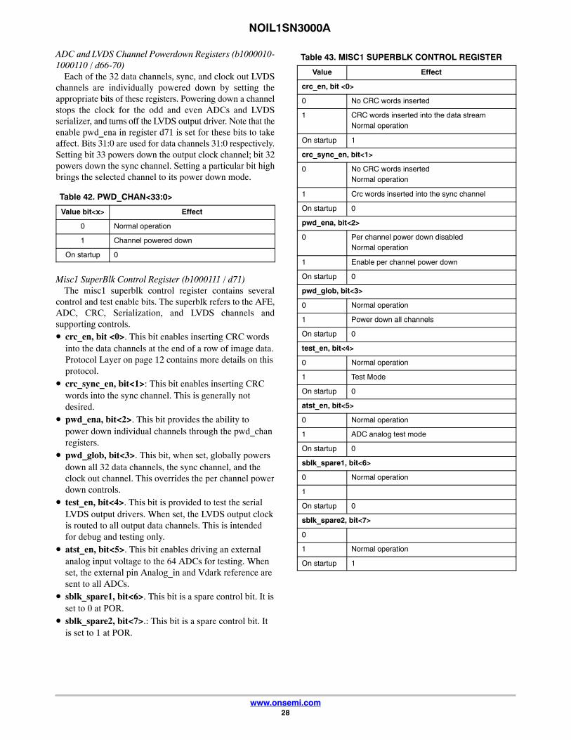
ADC and LVDS Channel Powerdown Registers (b1000010-1000110 / d66-70)
Each of the 32 data channels, sync, and clock out LVDSchannels are individually powered down by setting theappropriate bits of these registers. Powering down a channelstops the clock for the odd and even ADCs and LVDSserializer, and turns off the LVDS output driver. Note that theenable pwd_ena in register d71 is set for these bits to takeaffect. Bits 31:0 are used for data channels 31:0 respectively.Setting bit 33 powers down the output clock channel; bit 32powers down the sync channel. Setting a particular bit highbrings the selected channel to its power down mode.
Table 42. PWD_CHAN<33:0>
Value bit<x> Effect
0 Normal operation
1 Channel powered down
On startup 0
Misc1 SuperBlk Control Register (b1000111 / d71)The misc1 superblk control register contains several
control and test enable bits. The superblk refers to the AFE,ADC, CRC, Serialization, and LVDS channels andsupporting controls.• crc_en, bit <0>. This bit enables inserting CRC words
into the data channels at the end of a row of image data.Protocol Layer on page 12 contains more details on thisprotocol.
• crc_sync_en, bit<1>: This bit enables inserting CRCwords into the sync channel. This is generally notdesired.
• pwd_ena, bit<2>. This bit provides the ability topower down individual channels through the pwd_chanregisters.
• pwd_glob, bit<3>. This bit, when set, globally powersdown all 32 data channels, the sync channel, and theclock out channel. This overrides the per channel powerdown controls.
• test_en, bit<4>. This bit is provided to test the serialLVDS output drivers. When set, the LVDS output clockis routed to all output data channels. This is intendedfor debug and testing only.
• atst_en, bit<5>. This bit enables driving an externalanalog input voltage to the 64 ADCs for testing. Whenset, the external pin Analog_in and Vdark reference aresent to all ADCs.
• sblk_spare1, bit<6>. This bit is a spare control bit. It isset to 0 at POR.
• sblk_spare2, bit<7>.: This bit is a spare control bit. Itis set to 1 at POR.
Table 43. MISC1 SUPERBLK CONTROL REGISTER
Value Effect
crc_en, bit <0>
0 No CRC words inserted
1 CRC words inserted into the data streamNormal operation
On startup 1
crc_sync_en, bit<1>
0 No CRC words insertedNormal operation
1 Crc words inserted into the sync channel
On startup 0
pwd_ena, bit<2>
0 Per channel power down disabledNormal operation
1 Enable per channel power down
On startup 0
pwd_glob, bit<3>
0 Normal operation
1 Power down all channels
On startup 0
test_en, bit<4>
0 Normal operation
1 Test Mode
On startup 0
atst_en, bit<5>
0 Normal operation
1 ADC analog test mode
On startup 0
sblk_spare1, bit<6>
0 Normal operation
1
On startup 0
sblk_spare2, bit<7>
0
1 Normal operation
On startup 1
NOIL1SN3000A
www.onsemi.com29
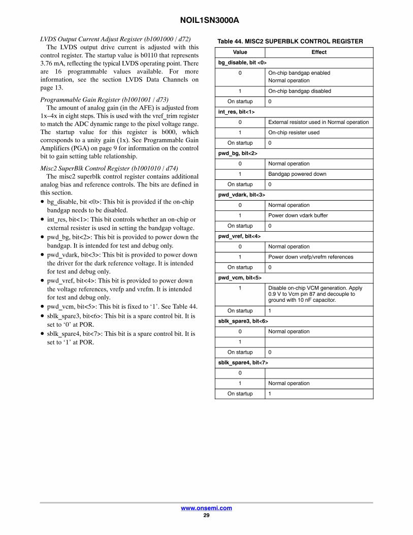
LVDS Output Current Adjust Register (b1001000 / d72)The LVDS output drive current is adjusted with this
control register. The startup value is b0110 that represents3.76 mA, reflecting the typical LVDS operating point. Thereare 16 programmable values available. For moreinformation, see the section LVDS Data Channels onpage 13.
Programmable Gain Register (b1001001 / d73)The amount of analog gain (in the AFE) is adjusted from
1x–4x in eight steps. This is used with the vref_trim registerto match the ADC dynamic range to the pixel voltage range.The startup value for this register is b000, whichcorresponds to a unity gain (1x). See Programmable GainAmplifiers (PGA) on page 9 for information on the controlbit to gain setting table relationship.
Misc2 SuperBlk Control Register (b1001010 / d74)The misc2 superblk control register contains additional
analog bias and reference controls. The bits are defined inthis section.• bg_disable, bit <0>: This bit is provided if the on-chip
bandgap needs to be disabled.• int_res, bit<1>: This bit controls whether an on-chip or
external resister is used in setting the bandgap voltage.• pwd_bg, bit<2>: This bit is provided to power down the
bandgap. It is intended for test and debug only.• pwd_vdark, bit<3>: This bit is provided to power down
the driver for the dark reference voltage. It is intendedfor test and debug only.
• pwd_vref, bit<4>: This bit is provided to power downthe voltage references, vrefp and vrefm. It is intendedfor test and debug only.
• pwd_vcm, bit<5>: This bit is fixed to ‘1’. See Table 44.
• sblk_spare3, bit<6>: This bit is a spare control bit. It isset to ‘0’ at POR.
• sblk_spare4, bit<7>: This bit is a spare control bit. It isset to ‘1’ at POR.
Table 44. MISC2 SUPERBLK CONTROL REGISTER
Value Effect
bg_disable, bit <0>
0 On-chip bandgap enabledNormal operation
1 On-chip bandgap disabled
On startup 0
int_res, bit<1>
0 External resistor used in Normal operation
1 On-chip resister used
On startup 0
pwd_bg, bit<2>
0 Normal operation
1 Bandgap powered down
On startup 0
pwd_vdark, bit<3>
0 Normal operation
1 Power down vdark buffer
On startup 0
pwd_vref, bit<4>
0 Normal operation
1 Power down vrefp/vrefm references
On startup 0
pwd_vcm, bit<5>
1 Disable on-chip VCM generation. Apply0.9 V to Vcm pin 87 and decouple toground with 10 nF capacitor.
On startup 1
sblk_spare3, bit<6>
0 Normal operation
1
On startup 0
sblk_spare4, bit<7>
0
1 Normal operation
On startup 1

NOIL1SN3000A
www.onsemi.com30
Testpattern 0-31 Registers (b1100000- 1111111 / d96-127)A register is provided for each of the 32 data channels for
LVDS data recovery calibration, alignment, and testing. Aunique test pattern is programmed for each data channel and
routed to the LVDS outputs by bypassing the ADCs anddisabling the training mode (setting bypass_en and clearingtraining_en, both contained in register d11).
Table 45. TEST PATTERN REGISTERS
Register Startup Value
Testpattern0 b00000001
Testpattern1 b00000001
Testpattern2 b00000010
Testpattern3 b00000010
Testpattern4 b00000100
Testpattern5 b00000100
Testpattern6 b00001000
Testpattern7 b00001000
Testpattern8 b00010000
Testpattern9 b00010000
Testpattern10 b00100000
Testpattern11 b00100000
Testpattern12 b01000000
Testpattern13 b01000000
Testpattern14 b10000000
Testpattern15 b10000000
Testpattern16 b10000000
Testpattern17 b10000000
Testpattern18 b01000000
Testpattern19 b01000000
Testpattern20 b00100000
Testpattern21 b00100000
Testpattern22 b00010000
Testpattern23 b00010000
Testpattern24 b00001000
Testpattern25 b00001000
Testpattern26 b00000100
Testpattern27 b00000100
Testpattern28 b00000010
Testpattern29 b00000010
Testpattern30 b00000000
Testpattern31 b00000000

NOIL1SN3000A
www.onsemi.com31
Serial Peripheral Interface (SPI )The SPI registers have an address space of 7 bits,
a<6>–a<0>, and 8 data bits, d<7>–d<0>. A singleinstruction bit chooses between a read or write instruction.
The SPI is used only after the clock has started and the chipis not in reset. Otherwise, the SPI register is kept in reset. SPIregisters are reset to their default value by bringingRESET_N low. The SPI bit RESET_N_SEQ has no effecton the SPI bits.
Setup and hold requirements of interface signals relativeto SPI_CLK are for both requirements 2.5 ns. Output delayis 1.5 ns after falling edge of SPI_CLK. Rise time (10% to90%) is 9 ns assuming a 18 pF load. To upload SPI, followthis sequence:
Disable sequencer Upload through SPI Enablesequencer
Read Sequence, C=0The part is selected by pulling CS low. The 1-bit
instruction (READ) is transmitted to the image sensor,followed by the 7-bit address (A6 through A0). Theinstruction and address bits are clocked in on the rising edgeof the clock. After the correct READ instruction and addressare sent, the data stored in the memory at the selected addressis shifted out on the MISO pin. The data bits are shifted outon the first falling edge after the last address bit is clocked.The read operation is terminated by raising the CS pin. Themaximum operating frequency is 10 MHz.
NOTE: SPI settings cannot be uploaded during readout.
Figure 16. SPI Read Timing
Write Sequence, C=1The image sensor is selected by pulling CS low. The
WRITE instruction is issued, followed by the 7-bit address,and then the 8-bit data. All data is clocked in on the risingedge of the clock.
To write the data to the array, the CS is brought high afterthe least significant bit (D0) of the data byte is clocked in. IfCS is brought high at any other time, the write operation isnot completed. Maximum operating frequency is 10 MHz.
Figure 17. SPI Write Timing
NOIL1SN3000A
www.onsemi.com32
OPERATING MODES
This sensor supports multiple operation modes. Thefollowing list provides an overview.• Global shutter mode
♦ Pipelined global shutter mode• Master mode• Slave mode
♦ Triggered global shutter mode• Master mode• Slave mode
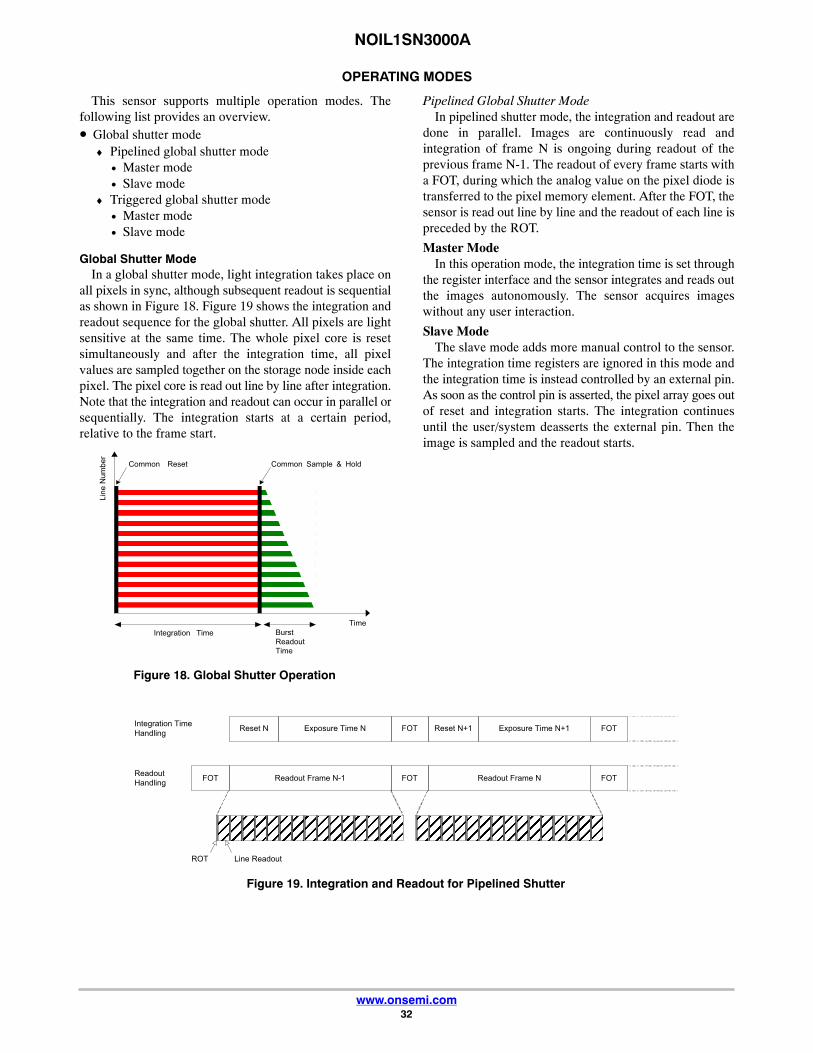
Global Shutter ModeIn a global shutter mode, light integration takes place on
all pixels in sync, although subsequent readout is sequentialas shown in Figure 18. Figure 19 shows the integration andreadout sequence for the global shutter. All pixels are lightsensitive at the same time. The whole pixel core is resetsimultaneously and after the integration time, all pixelvalues are sampled together on the storage node inside eachpixel. The pixel core is read out line by line after integration.Note that the integration and readout can occur in parallel orsequentially. The integration starts at a certain period,relative to the frame start.
Figure 18. Global Shutter Operation
Lin
e N
um
ber
ÊÊÊÊÊÊÊÊÊÊÊÊÊÊÊÊÊÊÊÊÊÊÊÊÊÊÊÊÊÊÊÊÊÊÊÊÊÊÊÊÊÊÊÊÊÊÊÊÊÊÊÊÊÊÊÊ
Time
ÊÊÊÊÊÊÊÊÊÊÊÊÊÊÊÊÊÊÊÊÊÊÊÊÊÊÊÊ
Integration Time Burst
ReadoutTime
Common Reset Common Sample & Hold
Pipelined Global Shutter ModeIn pipelined shutter mode, the integration and readout are
done in parallel. Images are continuously read andintegration of frame N is ongoing during readout of theprevious frame N-1. The readout of every frame starts witha FOT, during which the analog value on the pixel diode istransferred to the pixel memory element. After the FOT, thesensor is read out line by line and the readout of each line ispreceded by the ROT.
Master ModeIn this operation mode, the integration time is set through
the register interface and the sensor integrates and reads outthe images autonomously. The sensor acquires imageswithout any user interaction.
Slave ModeThe slave mode adds more manual control to the sensor.
The integration time registers are ignored in this mode andthe integration time is instead controlled by an external pin.As soon as the control pin is asserted, the pixel array goes outof reset and integration starts. The integration continuesuntil the user/system deasserts the external pin. Then theimage is sampled and the readout starts.
Figure 19. Integration and Readout for Pipelined Shutter
Reset N Exposure Time N Reset N+1 Exposure Time N+1
Readout Frame N-1 FOTFOT Readout Frame N
ÉÉÉ
ÉÉÉÉÉÉ
ÉÉÉ
ÉÉÉÉÉÉ
ÉÉÉÉÉÉ
ÉÉÉ
ÉÉÉÉÉÉ
ÉÉÉ
ÉÉÉÉÉÉ
ÉÉÉÉÉÉ
ÉÉÉ
ÉÉÉÉÉÉ
ÉÉÉ
ÉÉÉ
ÉÉÉÉÉÉ
FOT
Integration Time
Handling
Readout
Handling
ÉÉÉ
ÉÉÉÉÉÉ
ÉÉÉÉÉÉ
ÉÉÉ
ÉÉÉÉÉÉ
ÉÉÉ
ÉÉÉÉÉÉ
ÉÉÉÉÉÉ
ÉÉÉ
ÉÉÉÉÉÉ
ÉÉÉ
ÉÉÉÉÉÉ
ÉÉÉÉÉÉ
ÉÉÉÉÉÉ
ÉÉÉROT Line Readout
FOT FOT
NOIL1SN3000A
www.onsemi.com33
Figure 20. Pipelined Shutter Operated in Slave Mode
Reset N Exposure Time N Reset N+1 Exposure Time N+1
Readout N-1 FOTFOT Readout N
ÉÉÉÉÉÉÉÉÉÉÉÉÉÉÉÉÉÉÉÉÉÉÉÉÉÉÉÉÉÉÉÉÉÉÉÉÉÉÉÉÉÉ
ÉÉ
ÉÉÉÉ
FOT
Integration Time
Handling
Readout
Handling
ÉÉÉÉÉÉÉÉÉÉÉÉÉÉÉÉÉÉÉÉÉÉÉÉÉÉÉÉÉÉÉÉÉÉÉÉÉÉ
ÉÉÉÉ
ÉÉ
ROT Line Readout
External Trigger
FOT FOT
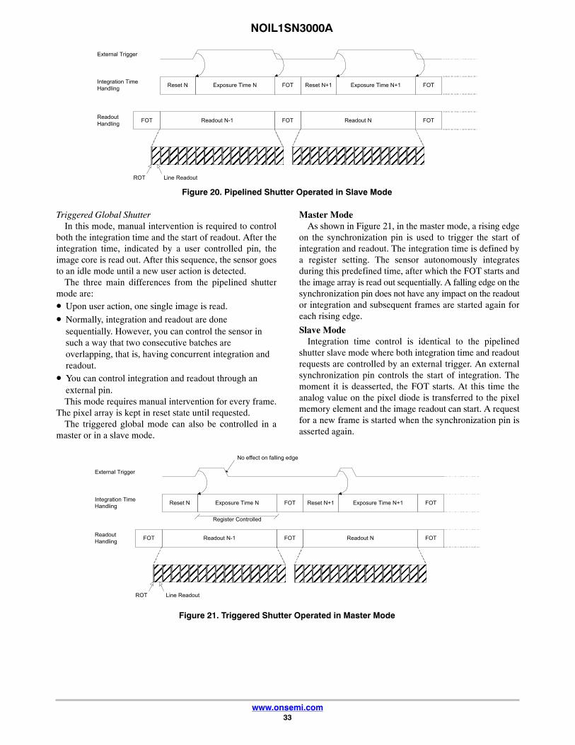
Triggered Global ShutterIn this mode, manual intervention is required to control
both the integration time and the start of readout. After theintegration time, indicated by a user controlled pin, theimage core is read out. After this sequence, the sensor goesto an idle mode until a new user action is detected.
The three main differences from the pipelined shuttermode are:• Upon user action, one single image is read.
• Normally, integration and readout are donesequentially. However, you can control the sensor insuch a way that two consecutive batches areoverlapping, that is, having concurrent integration andreadout.
• You can control integration and readout through anexternal pin.This mode requires manual intervention for every frame.
The pixel array is kept in reset state until requested.The triggered global mode can also be controlled in a
master or in a slave mode.
Master ModeAs shown in Figure 21, in the master mode, a rising edge
on the synchronization pin is used to trigger the start ofintegration and readout. The integration time is defined bya register setting. The sensor autonomously integratesduring this predefined time, after which the FOT starts andthe image array is read out sequentially. A falling edge on thesynchronization pin does not have any impact on the readoutor integration and subsequent frames are started again foreach rising edge.
Slave ModeIntegration time control is identical to the pipelined
shutter slave mode where both integration time and readoutrequests are controlled by an external trigger. An externalsynchronization pin controls the start of integration. Themoment it is deasserted, the FOT starts. At this time theanalog value on the pixel diode is transferred to the pixelmemory element and the image readout can start. A requestfor a new frame is started when the synchronization pin isasserted again.
Figure 21. Triggered Shutter Operated in Master Mode
Reset N Exposure Time N Reset N+1 Exposure Time N+1
Readout N-1 FOTFOT Readout N
ÉÉÉÉÉÉÉÉÉÉÉÉÉÉÉÉÉÉÉÉÉÉÉÉÉÉÉÉÉÉÉÉÉÉÉÉÉÉÉÉ
ÉÉ
ÉÉÉÉ
FOT
Integration Time
Handling
Readout
Handling
ÉÉÉÉÉÉÉÉÉÉÉÉÉÉÉÉÉÉÉÉÉÉÉÉÉÉÉÉÉÉÉÉÉÉÉÉÉÉÉÉ
ÉÉÉÉ
ÉÉ
ROT Line Readout
External Trigger
No effect on falling edge
Register Controlled
FOT FOT

NOIL1SN3000A
www.onsemi.com34
IMAGE SENSOR TIMING AND READOUT
Pixel TimingAfter every exposure cycle, the value on the pixel diode
is transferred to the pixel storage capacitor. This iscontrolled by Vmem, precharge, and sample signals. Theduration of this operation is the FOT. At the beginning of theFOT, Vmem is brought low, and precharge and sample arebrought high. The precharge pulse ensures that the oldinformation on the storage node is destroyed. This ensuresthere is no image lag. After the falling edge of the prechargepulse, the sampling operation on the storage node iscompleted during the high level of sample.
After the falling edge of sample, Vmem is brought high.The rise in Vmem compensates for the voltage loss in the lastsource follower in the pixel. The readout begins after this.The pulse length is controlled by the user. The registers thatcontrol this are listed in the following section.
Considerations in Pixel TimingThe length of the FOT_TIMER, PRECHARGE_TIMER,
and SAMPLE_TIMER influences the final image quality.• Precharge pulse: The pixel precharge prevents image
lag. A very short pulse results in image lag.• Sample pulse: A shorter sample results in a reduced
dark level.• FOT_TIMER register: The vmem signal must charge
all pixel storage capacitors simultaneously. This is alarge combined capacitance (96 nF) and Vmem takessome time to stabilize. Readout must start only afterVmem is stable.The length of pixel_reset influences image lag. The pixel
must be reset for at least 3 s.
Figure 22. Pixel Timing
Frame Rate and Windowing
Frame RateThe frame rate depends on the input clock, FOT, and ROT.
The frame period is calculated as follows:1 kernel = 32 pixels1 granularity clock = 4 clock periodsFrame period = FOT + Nr. lines x (ROT + Nr. pixels/4 x
data period)OrFrame period = FOT + Nr. lines x (ROT + Nr. kernels *
granularity clock cycles)
ExampleReadout time for full resolution at nominal speed of 206
MHz (4.854 ns) is given byFrame period = 3.2 s + (1710 x (176 ns + 1696/4 x 2.427
ns)) = 2.063 msOrFrame period = 3.2 s + (1710 x (176 ns + 53 x 19.4174
ns)) = 2.063 msFrame Rate = 485 fpsAlternatively, frame rate can also be expressed in terms of
reset length and integration time rather than readout time.
Table 46. CLARIFICATION OF FRAME RATEPARAMETERS
Parameter Comment Clarification
FOT Frame overheadtime
The FOT does a frametransfer from pixel diode topixel storage node. Duringthis transfer, the sensor isnot read out. The FOTlength is programmable.The default length is 3.2 s.
ROT Row overheadtime
The ROT transfers the pixeloutput to the column amplifi-ers. Default ROT is 176 ns.
Nr. lines Number of linesread out in eachframe
Default is 1710 lines.
Nr. pixels Number of pixelsread out in eachline
Default is 1696 pixels.
Data period 0.5 x clock period= 2.427 ns
Because the outputs oper-ate at DDR, the data periodis half the clock period(206 MHz clk).

NOIL1SN3000A
www.onsemi.com35
The sequence of events shown in Figure 23 occurs duringintegration and readout in pipelined global shutter mode.
Frame period = FOT + Reset length + Integration time= t1+t2+t3To receive the frames without any overlap, the sum of
reset time and integration time should always be greater thanthe readout time.
(Reset time + Integration time) > Readout timeIn global shutter mode, the whole pixel array is integrated
simultaneously. For more information, seeON Semiconductor application note AN57864, Frame RateBased on Integration Time.
Figure 23. Timing Diagram
WindowingWindowing is easily achieved by SPI. The starting point
of the x and y address and the window size can be uploaded.The minimum step size is in the x-direction is 32 pixels(choose only multiples of 32 as a start or stop addresses). Theminimum step in the y-direction is 1 line (every line can beaddressed in the normal mode).
Table 47. TYPICAL FRAME RATES AT 206 MHz
Image Resolution (x * y)
Frame Rate(fps)
Frame Period (ms)
1696 x 1710 485 2.065
1600 x 1200 712 1.404
1280 x 1024 1001 1.000
640 x 480 2653 0.377
512 x 512 3808 0.263
256 x 256 10704 0.093
128 x 128 26178 0.038
Digital SignalsLUPA3000 can operate in slave mode. To do so, the pixel
array of the image sensor requires different digital controlsignals. The function of each signal is listed in Table 48.
Table 48. OVERVIEW OF DIGITAL SIGNALS
Signal Name I/O Comments
FOT Output Output pin for FOT
ROT Output Output pin for ROT
Exposure_2 Input Integration pin dual slope
Exposure_1 Input Integration pin first slope
RESET_N Input Sequencer reset, active LOW
CLK Input System clock (206 MHz)
SPI_CS Input SPI chip select
SPI_CLK Input SPI clock
SPI_MOSI Input Data line of the SPI, serial input
SPI_MISO Output Data line of the SPI, serial output

NOIL1SN3000A
www.onsemi.com36
Image Format and Readout ProtocolThe active area read out by the sequencer in full frame
mode is shown in Figure 24. Pixels are always read inmultiples of 32.
Figure 24. Sensor Read Out Format
32 pixelsTimeslot 1
32 pixelsTimeslot 53
Sensor Timing and Readout
High Level TimingThe LUPA3000 sensor is a pipelined synchronous shutter.
This indicates that light integration and readout occur inparallel, achieving the high frame rate and data throughput.
The maximum frame rate of the sensor is determined bythe time needed to readout a full frame. This frame time isseparated in the FOT and the time to readout all lines. Thereadout of a line is separated in a ROT and the readout of allkernels.
Integration TimingThe integration time is controlled through the
EXPOSURE_1 pin. The rising edge of EXPOSUREdetermines the start of exposure and the falling edge ofEXPOSURE_1 starts the FOT and determines the end of theintegration time.
The falling edge of the internal pixel reset pulse causes avisible crosstalk in the image, unless the edge occurs in thebeginning of the ROT during readout. As a result, theEXPOSURE pulse is internally delayed until the next ROT.The duration of this delay depends on the length of the linebeing readout. If the EXPOSURE_1 is after Lx is finished,then integration starts immediately. There is no need to waitfor ROT.
The internal timing of the FOT is controlled by thesequencer. The length of the FOT is set by the SPI registersPRECHARGE_TIMER, SAMPLE_TIMER,VMEM_TIMER, and FOT_TIMER.
Ensure that pixel_reset is high for at least 3 s.
FOT Starts After ReadoutThis is the normal situation where a full window is
readout. A full window refers to the resolution set by theY_START, Y_END, and NB_OF_KERNELS register. Thismay be the full resolution or a partial window. Figure 26shows a high level timing; ‘Lx’ refers to ‘line x’.
When EXPOSURE_1 goes low, the FOT beginsimmediately. Integration time continues until the fallingedge of pix_sample. The falling edge of pix_sample is afixed amount of time after the falling edge ofEXPOSURE_1. This time is set SAMPLE_TIMER (seeFrame Overhead Time).
Figure 25. Pipelined Operation
L1710FOT_ _ _
K53ROT_ _ _
Readout frame I+1Readout frame I
Integration frame I+2Integration frame I+1
Readout Lines
Readout Pixels
L1 L2
K1 K2
Figure 26. High Level Readout Timing
L1 L2 L3 xL
SAMPLE_TIMER
integration time
FOTFOT
pix_vmem
DATA
EXPOSURE_1
pix_reset
pix_sample
wait till ROT

NOIL1SN3000A
www.onsemi.com37
.FOT starts before readout. When the EXPOSURE_1 signal goes low before the window readout has finished, the readoutis interrupted after the completion of the current line’s readout (line x in Figure 27).
Figure 27. High Level Readout Timing
L1 L2 L3 L x-1 x L1L
wait till ROT
integration time
FOTFOT
pix_vmem
DATA
EXPOSURE_1
pix_reset
pix_sample
wait till ROT
Dual Slope Integration TimingIf the dual slope enable bit is set high, dual slope
integration is controlled through the EXPOSURE_2 pin. Ifthe dual slope enable bit is set low, the dual slope integrationis disabled. Figure 28 shows the timing. The pix_reset signalis controlled by the EXPOSURE_1 pin. When pix_resetgoes low, the dual slope reset of the pixel array is activated.Bringing the EXPOSURE_2 pin high starts the dual slopeintegration. The start of FOT is controlled by the falling edge
of the EXPOSURE_1 pin. The EXPOSURE_2 pin must bebrought low during FOT to be ready for the next cycle.
Setup and Hold RequirementsEXPOSURE_1 and EXPOSURE_2 are deglitched using
two chained flipflops that clock on the sensor clock. As aresult, there is no setup requirement for both signals relativeto LVDS_CLKIN. The hold requirement is 15 clock periodsof LVDS_CLKIN.
Figure 28. Dual Slope Integration Timing
L1 L2 L3 L4 xL
wait till ROT
DS integration time
integration time
FOTFOT
pix_vmem
DATA
EXPOSURE_1
EXPOSURE_2
pix_reset
pix_reset_ds
pix_sample
wait till ROT
Readout ModesThe sensor is configured to operate in three readout
modes: training, test image readout, and normal readout.These modes enable correct communication between thesensor and the customer system.
Readout of Training SequenceBy setting the TRAINING_EN and BYPASS_MODE bit,
all data channels and the sync channel transmit alternatingthe Idle_A and Idle_B word. Rotating the received Idle_Aand Idle_B words in the receiver allows correcting for skewbetween the LVDS outputs and the receiver clock. You canprogram the Idle_A and Idle_B words.
Readout of Test ImageBy setting the BYPASS_MODE bit high and the
TRAINING_EN bit low, the sensor is configured to outputa programmable test pattern.
The sync channel operates as in normal readout andenables frame and line synchronization. Every data channeltransmits a fixed, programmable word to replace normaldata words coming from the ADC. In this mode, the sensorbehaves as in normal readout. The sync channel transmitsprogrammable keywords to allow frame and linesynchronization. When not transmitting data from the ADC,the data channels transmit the toggling Idle_A and Idle_Bwords. As a result, the data stream from the sensor has afixed format.
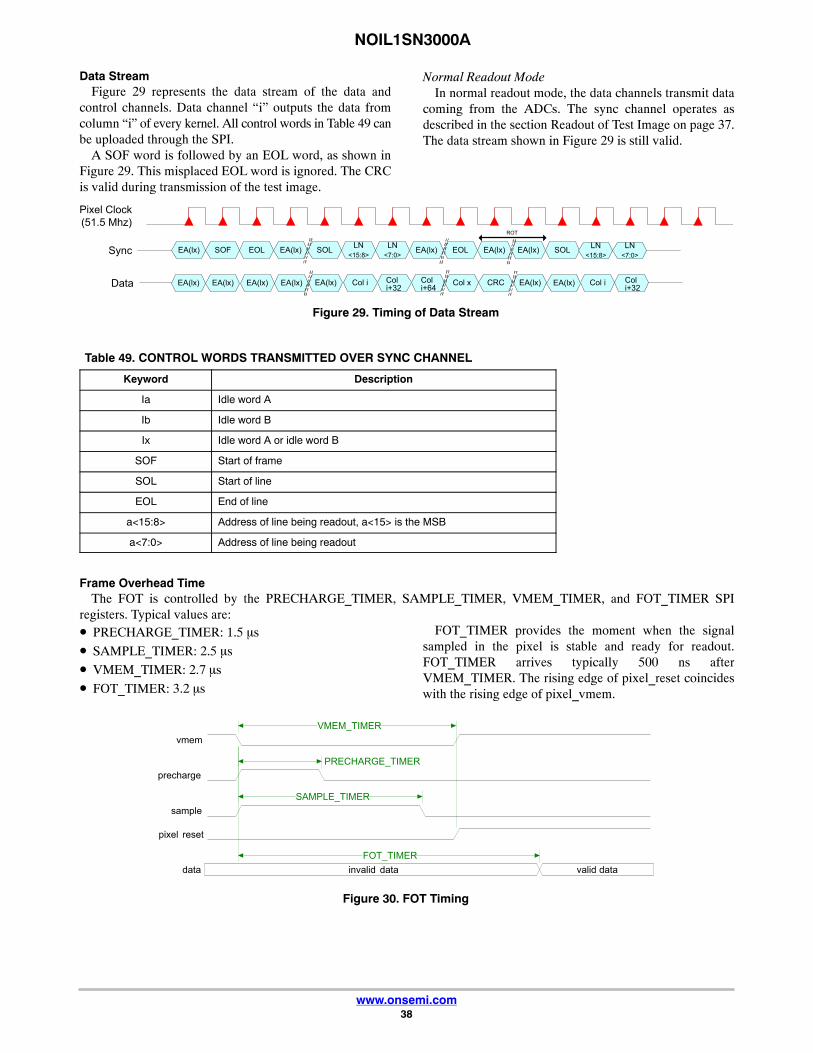
NOIL1SN3000A
www.onsemi.com38
Data StreamFigure 29 represents the data stream of the data and
control channels. Data channel “i” outputs the data fromcolumn “i” of every kernel. All control words in Table 49 canbe uploaded through the SPI.
A SOF word is followed by an EOL word, as shown inFigure 29. This misplaced EOL word is ignored. The CRCis valid during transmission of the test image.
Normal Readout ModeIn normal readout mode, the data channels transmit data
coming from the ADCs. The sync channel operates asdescribed in the section Readout of Test Image on page 37.The data stream shown in Figure 29 is still valid.
Figure 29. Timing of Data Stream
SOLLN
<15:8>
LN
<7:0>EA(lx)EA(lx) EOL EA(lx) EA(lx) SOL
Pixel Clock
(51.5 Mhz)
SOF EOL EA(lx)Sync
Col i Col x CRC Col iData
LN
<15:8>
LN
<7:0>
EA(lx)EA(lx)EA(lx)EA(lx) EA(lx) EA(lx) EA(lx)
ROT
Coli+32
Coli+64
Coli+32
Table 49. CONTROL WORDS TRANSMITTED OVER SYNC CHANNEL
Keyword Description
Ia Idle word A
Ib Idle word B
Ix Idle word A or idle word B
SOF Start of frame
SOL Start of line
EOL End of line
a<15:8> Address of line being readout, a<15> is the MSB
a<7:0> Address of line being readout
Frame Overhead TimeThe FOT is controlled by the PRECHARGE_TIMER, SAMPLE_TIMER, VMEM_TIMER, and FOT_TIMER SPI
registers. Typical values are:• PRECHARGE_TIMER: 1.5 s
• SAMPLE_TIMER: 2.5 s
• VMEM_TIMER: 2.7 s
• FOT_TIMER: 3.2 s
FOT_TIMER provides the moment when the signalsampled in the pixel is stable and ready for readout.FOT_TIMER arrives typically 500 ns afterVMEM_TIMER. The rising edge of pixel_reset coincideswith the rising edge of pixel_vmem.
Figure 30. FOT Timing
invalid data valid data
FOT_TIMER
SAMPLE_TIMER
PRECHARGE_TIMER
VMEM_TIMER
vmem
precharge
sample
pixel reset
data

NOIL1SN3000A
www.onsemi.com39
Reduced ROT Readout ModeWhen a row is selected, each pixel sees a large capacitive
load.This comes from two sections - 1) metal line connecting
the pixel output to the column amplifier and parasitic capsof the 1695 pixels connected to it. 2) The column amplifiercurrent source transistors. In normal ROT mode, both thestructures are on and to transfer the charge from the pixel tothe column amplifiers, each column amplifier must draw alarger current.
In the reduced ROT mode, the column amplifier currentsource is turned off/disabled. The capacitance of the columnitself acts like the sampling capacitor and the capacitanceseen by the pixel is reduced. As a result, the transfer of thecharge is faster and a reduced ROT can be used. In reducedROT mode, the dynamic range of the pixel is lesser than innormal ROT mode but the power consumption is alsoreduced.
The sensor operates in reduced ROT by default, with aROT of nine sensor clock periods (175 ns).
FOT and ROT Pin TimingThe chip has two pins (FOT and ROT) that indicate
internal FOT and ROT periods.
FOT PinThe actual FOT goes from the falling edge of the internal
VMEM signal to the rising edge of the first internal CLK_Y.After this rising edge of CLK_Y, the first ROT starts. TheFOT pin goes high at the same moment VMEM goes lowand remains high until one sensor clock period (CLKIN/4)before the end of the actual FOT. This is shown in Figure 31.
ROT PinThe actual ROT goes from the rising edge of the internal
CLK_Y signal to the falling edge of the internal SYNC_Xsignal. The ROT pin goes high at the rising edge of CLK_Yand remains high until one sensor clock (CLKIN/4) beforethe end of the actual ROT.
Table 50. FOT AND ROT PIN TIMING
Pin Delay vs. Sensor Clock Rise and Fall Times (20 pF Load)
FOT 2.5 ns 6 ns
ROT 2.5 ns 6 ns
Figure 31. FOT Pin Timing
1 SEN_CLK
actual FOT (FOT_TIMER * 4 SEN_CLK)
SEN_CLK
vmem
clk_y
FOT pin
Figure 32. ROT Pin Timing
1 SEN_CLK
actual ROT (ROT_TIMER + 2 SEN_CLK)
SEN_CLK
clk_y
sync_x
ROT pin
Asynchronous ResetThe sensor has a reset pin, RESET_N, and a reset SPI
register, RESET_N_SEQ. Both are active low.RESET_N is the chip reset. All components on the chip
are reset when this pin is low. This includes the sequencer,the SPI register, and X and Y shift registers. The reset isasynchronous.
RESET_N_SEQ is the sequencer reset. Bringing this bitlow only resets the sequencer. This is used to restart thesequencer with the current SPI settings.
Reset on StartupWhen the sensor starts up, RESET_N is kept low until all
supply voltages are stable. After the rising edge of
RESET_N, RESET_N_SEQ is kept low for an additional0.5 s.
During the chip reset the data on the LVDS outputs (datachannels and sync channel) is invalid. When the chip comesout of reset, but the sequencer is kept in reset, the LVDSoutputs toggle between the idle words.
If RESET_N_SEQ is only low for a short period of time(100 ns), the pixel array is not completely reset. Informationfrom the previous integration cycle is still present on thephotodiode. Ensure that the pixels are in reset for at least 3 sby keeping RESET_N_SEQ low for a long time, or by notstarting exposure before 3 s after RESET_N_SEQ.

NOIL1SN3000A
www.onsemi.com40
Figure 33. Reset on Startup
idle wordsidle words
min 0.5us
stable supply voltagesstable supply voltages
RESET_N
RESET_N_SEQ
LVDS output
Sequencer ResetThe sequencer is reset separately by bringing the
RESET_N_SEQ register low. This causes an asynchronousreset of the sequencer. The reset must have a length of at least20 clock cycles (five words). Resetting the sequencercorrupts the analog voltages stored in the pixel array.
Therefore, a new readout sequence must start with anexposure first. After the reset, a readout sequence isreinitiated by using EXPOSURE_1 pin. Ensure the reset ofthe pixel array is long enough ( 3 s).
Figure 34. Sequencer Reset
valid datavalid data
FOT+ROT
idle wordsidle words
pix_reset
min 20 clk cyclesmin 20 clk cycles
RESET_N_SEQ
EXPOSURE_1
LVDS outputs
Startup SequenceTo guarantee the correct startup of all the sensor modules,
perform the following startup sequence:1. All supplies are powered on simultaneous, but the
RESET_N pin is kept low. The VAA is notpowered on before VDD is powered on.
2. When all supplies are stable, bring RESET_N pinhigh. The sensor now begins to operate.
3. Set RESET_N_SEQ register bit to zero if otherSPI registers need to be uploaded.
4. Set the RESET_N_SEQ bit to 1 if all required SPIregisters are changed. LUPA3000 operates only inslave mode; therefore, the sensor is now controlledthrough the EXPOSURE_1 pin.

NOIL1SN3000A
www.onsemi.com41
ADDITIONAL FEATURES
WindowingA fully configurable window can be selected for readout.
The parameters to configure this window are:X_START: It is the start position for the X readout.
Readout starts only at odd kernel positions. As a resultpossible start positions are 64 columns (two kernels)separated from each other.
X_kernels: The number of kernels to be read out.Y_start: The starting line of the readout window.Y_end: The end line of the readout window,
granularity of 1.For windowing, the effective readout time is smaller than
in full frame mode, because only the relevant part of theimage array is accessed. As a result, it is possible to achievehigher frame rates.
Figure 35. Window Selected for Readout
1696 pixels
y-end
y-start
x-startx-end
1710 pixels
Restrictions to WindowingTo ensure correct operation of the sensor, the readout of
partial windows must be done with some restrictions.• The minimum window size is 4 kernels (128 pixels) in
the x-direction and 1 line in the y-direction.• In the x-direction, windowing can only start at an odd
kernel (kernel1, kernel3, and so on). Then number ofkernels to readout is not subject to an odd-evenrestriction.
• The sum of the ROT_TIMER and theNB_OF_KERNELS spi registers should always be aneven number.
This means that for a fixed ROT time, the window size canonly change in steps of 64 pixels. If the number of kernelsto readout is decreased with one and the ROT is already atthe minimum value, then the ROT time should be increasedwith one (clock cycle) to compensate. The framerateremains unchanged by this, but the data rate drops.
Sub SamplingNot supported by LUPA3000.
Reverse ScanNot supported by LUPA3000.
Multiple WindowsNot supported by LUPA3000.
Dual SlopesDynamic range can be extended by the dual slope
capability of the sensor. The four colored lines in Figure 36represents analog signals of the photodiode of four pixels,which decreases as a result of exposure. The slope isdetermined by the amount of light at each pixel (the morelight, the steeper the slope). When the pixels reach thesaturation level, the analog does not change despite furtherexposure. Without the dual slope capabilities, the pixels p3and p4 are saturated before the end of the exposure time, andno signal is received. However, when using dual slopes, theanalog signal is reset to a second reset level (lower than theoriginal) before the integration time ends. The analog signalstarts decreasing with the same slope as before, and pixelsthat were saturated before could be nonsaturated at read outtime. For pixels that never reach any of the reset levels (forexample, p1 and p2), there is no difference between singleand multiple slope operation.
By choosing the time stamps of the double slope resets(typical at 90%, configurable by the user), it is possible tohave a nonsaturated pixel value even for pixels that receivea huge amount of light.
The reset levels are configured through external (power)pins.

NOIL1SN3000A
www.onsemi.com42
Figure 36. Dynamic Range Extended by Double Slope Capability
In slave mode, you have full control through the pins Exposure 1 and Exposure 2. Configure the multiple slope parametersfor the application and interpret the pixel data accordingly.
Figure 37. Dual Slope Timing in Slave Mode
Off-Chip FPN CorrectionFPN is a kind of spatial noise, a noise that does not change
with time. FPN comes from two different sources. The firstsource involves the variations between individual pixels.Within a CMOS image sensor, the device is designed suchthat each pixel is identical to all the others.
Although each pixel is similar to all of the others withinthe array, there are slight variations. These variations arisefrom variations in threshold voltages and offsets of theamplifier within each pixel. Because these can vary for eachpixel within the pixel array; they are referred to as pixel FPN.
The second source of FPN involves the performancevariations of the amplifiers shared by each column of thepixel array. The information within the pixel array is read outon a column-by-column basis through these columnamplifiers. When one amplifier behaves slightly differentfrom another, the entire column can be affected. When this
happens, it results in what appears to be vertical lines in theimage. This is commonly called column FPN. Of the twosources of FPN, column FPN is more noticeable than pixelFPN.
LUPA3000 has no on-chip FPN correction so it must becorrected off-chip in the software.
FPN can be calibrated off-chip by subtracting a darkimage from all captured images. For optimal results twoguidelines can be followed:• Use an averaged dark image to calibrate FPN; this
eliminates other noise sources that are present in thedark image.
• Use a different dark image to calibrate for differentoperation conditions. Different operation conditions canbe changes in temperature, FOT and ROT timing, andgain settings.

NOIL1SN3000A
www.onsemi.com43
Software FPN CorrectionThe procedure is as follows:
1. Adjust the black level with the help of histogramby modifying DAC offset.
2. Store a dark image by closing the lens aperture,but make sure no value is absolute zero.
3. Subtract the dark reference image from all thecaptured images.
Off-Chip PRNU CorrectionPixel response non-uniformity (PRNU) is also a kind of
spatial noise. It refers to the slight variations in response tothe same input that each pixel has due to the slight activeresponse variations between the amplifiers within differentpixels. Even though every pixel is carefully designed tomatch one another, slight variations in processing, noise,and other areas can cause these amplifiers to behavedifferently.
This is corrected with the help of a grey image; thecorrection is done by equalization of gain.
The procedure is as follows:1. Capture the grey image under the same condition
as the dark image.2. Open the aperture of the lens to allow light and
then capture the grey frame. All the pixels in thegrey image should have a grey value ofapproximately 70% white (histogram should peakat 70% white and the distribution should beuniform around the peak as much as possible).This grey image is stored.
FPN and PRNU correction formula:Vn = (Avg(Wn) / [Wn - Bn + 1]) x (Gn - Bn)Vn - data of a pixel after a calibrationGn - data of a pixel before carrying out a calibrationBn - black calibration data of the pixelWn - white (gray) calibration data of the pixel

NOIL1SN3000A
www.onsemi.com44
PACKAGE INFORMATION
Pin DefinitionsThe package has 369 pins. Table 51 lists 228 pins. The remaining pins are used as die attach ground pins.
Table 51. PIN LIST
Finger Number Pin Number Function Description
1 A3 GNDd_hs Ground high speed digital
2 B3 Vdd_hs 2.5-V high speed digital
3 A2 Clk_Outp Output clock P
4 B2 CLK_Outn Output clock N
5 A1 Outp 0 LVDS data output
6 B1 Outn 0 LVDS data output
7 C4 Outp 1 LVDS data output
8 D4 Outn 1 LVDS data output
9 C3 Outp 2 LVDS data output
10 D3 Outn 2 LVDS data output
11 C2 Outp 3 LVDS data output
12 D2 Outn 3 LVDS data output
13 C1 Outp 4 LVDS data output
14 D1 Outn 4 LVDS data output
15 E5 Outp 5 LVDS data output
16 F5 Outn 5 LVDS data output
17 E4 Vlvds 2.5-V LVDS
18 F4 GNDlvds Ground LVDS
19 E3 Outp 6 LVDS data output
20 F3 Outn 6 LVDS data output
21 E2 Outp 7 LVDS data output
22 F2 Outn 7 LVDS data output
23 E1 Outp 8 LVDS data output
24 F1 Outn 8 LVDS data output
25 G5 Outp 9 LVDS data output
26 H5 Outn 9 LVDS data output
27 G4 Outp 10 LVDS data output
28 H4 Outn 10 LVDS data output
29 G3 Outp 11 LVDS data output
30 H3 Outn 11 LVDS data output
31 G2 Outp 12 LVDS data output
32 H2 Outn 12 LVDS data output
33 G1 Vlvds 2.5-V LVDS
34 H1 GNDlvds Ground LVDS
35 J5 Outp 13 LVDS data output
36 K5 Outn 13 LVDS data output
37 J4 Outp 14 LVDS data output
38 K4 Outn 14 LVDS data output
39 J3 Outp 15 LVDS data output

NOIL1SN3000A
www.onsemi.com45
Table 51. PIN LIST
Finger Number DescriptionFunctionPin Number
40 K3 Outn 15 LVDS data output
41 J2 Vadc 2.5-V ADC
42 K2 GNDadc Ground ADC
43 J1 Outp 16 LVDS data output
44 K1 Outn 16 LVDS data output
45 L5 Outp 17 LVDS data output
46 M5 Outn 17 LVDS data output
47 L4 Outp 18 LVDS data output
48 M4 Outn 18 LVDS data output
49 L3 Vlvds 2.5-V LVDS
50 M3 GNDlvds Ground LVDS
51 L2 Outp 19 LVDS data output
52 M2 Outn 19 LVDS data output
53 L1 Outp 20 LVDS data output
54 M1 Outn 20 LVDS data output
55 N5 Outp 21 LVDS data output
56 P5 Outn 21 LVDS data output
57 N4 Outp 22 LVDS data output
58 P4 Outn 22 LVDS data output
59 N3 Outp 23 LVDS data output
60 P3 Outn 23 LVDS data output
61 N2 Outp 24 LVDS data output
62 P2 Outn 24 LVDS data output
63 N1 Outp 25 LVDS data output
64 P1 Outn 25 LVDS data output
65 R5 Vlvds 2.5-V LVDS
66 T5 GNDlvds Ground LVDS
67 R4 Outp 26 LVDS data output
68 T4 Outn 26 LVDS data output
69 R3 Outp 27 LVDS data output
70 T3 Outn 27 LVDS data output
71 R2 Outp 28 LVDS data output
72 T2 Outn 28 LVDS data output
73 R1 Outp 29 LVDS data output
74 T1 Outn 29 LVDS data output
75 U4 Outp 30 LVDS data output
76 V4 Outn 30 LVDS data output
77 U3 Outp 31 LVDS data output
78 V3 Outn 31 LVDS data output
79 U2 Clk_inp LVDS input clock
80 V2 Clk_inn LVDS input clock
81 U1 Syncp LVDS sync channel
NOIL1SN3000A
www.onsemi.com46
Table 51. PIN LIST
Finger Number DescriptionFunctionPin Number
82 V1 Syncn LVDS sync channel
83 W1 Vdd_hs 2.5-V high speed digital
84 W2 GNDd_hs Ground high speed digital
85 W3 GNDd_hs Ground high speed digital
86 W4 Vdd_hs 2.5-V high speed digital
87 W5 Vcm Decoupling analog reference voltage
88 W6 Vdark Decoupling analog reference voltage
89 V5 GNDadc Ground ADC
90 U5 Vadc 2.5-V ADC
91 V6 GNDd Ground digital
92 U6 Vdd 2.5-V digital
93 T6 GNDadc Ground ADC
94 T7 Vadc 2.5-V ADC
95 V7 GNDadc Ground ADC
96 U7 Vadc 2.5-V ADC
97 W7 GNDd Ground digital
98 W8 Vdd 2.5-V digital
99 V8 GNDaa Ground analog
100 U8 GNDaa Ground analog
101 T8 GNDaa Ground analog
102 W9 Vaa 2.5-V analog
103 V9 Vaa 2.5-V analog
104 U9 GNDaa Ground analog
105 T9 GNDaa Ground analog
106 W10 Vaa 2.5-V analog
107 V10 Vaa 2.5-V analog
108 U10 GNDaa Ground analog
109 T10 Vaa 2.5-V analog
110 W11 Vpix Vpix (typically 2.5 V)
111 V11 GNDd Ground digital
112 U11 Vdd 2.5-V digital
113 T11 Not Assigned Not assigned
114 T12 Not Assigned Not assigned
115 U12 Reset_n Digital input
116 V12 Exposure 1 Digital input
117 W12 Exposure 2 Digital input
118 W13 ROT Digital output
119 V13 FOT Digital output
120 U13 Not Assigned Not assigned
121 T13 Current_Ref_1 Current reference resistor
122 T14 Not Assigned Not assigned
123 U14 Analog_Out Analog output (leave floating)

NOIL1SN3000A
www.onsemi.com47
Table 51. PIN LIST
Finger Number DescriptionFunctionPin Number
124 V14 Not Assigned Not assigned
125 W14 Not Assigned Not assigned
126 W15 EOS_x End of Scan in x−direction. For test purpose only.Leave floating.
127 V15 SPI_MISO Digital output
128 U15 SPI_MOSI Digital input
129 T15 SPI_CLK Digital input
130 T16 SPI_CS Digital input
131 U16 GNDd Ground digital
132 V16 Vdd 2.5-V digital
133 W16 Vpix Vpix (typically 2.5 V)
134 W17 GNDesd Ground for ESD
135 V17 Not Assigned Not assigned
136 U17 Not Assigned Not assigned
137 T17 Test_Array Not assigned
138 T18 Full_Diode Not assigned
139 U18 Not Assigned Not assigned
140 V18 Not Assigned Not assigned
141 W18 EOSy_right End of Scan in y−direction. For test purpose only.Leave floating.
142 V19 GNDd Ground digital
143 U19 Vdd 2.5-V digital
144 W19 Vpix Vpix (typically 2.5 V)
145 W20 Precharge_Bias_2 Leave floating
146 V20 GNDesd Ground for ESD
147 U20 Not Assigned Not assigned
148 W21 GNDdrivers Ground array drivers
149 V21 Vres_ds Reset DS supply (typically 2.5 V)
150 U21 Vres Reset suppy (typically 3.3 V)
151 T21 Vmem_l Vmem low supply (typically 2.5 V)
152 T20 Vmem_h Vmem high supply (typically 3.3 V)
153 R20 Vprecharge Pix precharge supply
154 R21 D/A Ground Die attach ground
155 P21 Vdd 2.5-V digital
156 P20 Not Assigned Not assigned
157 N20 GNDdrivers Ground array drivers
158 N21 Vres_ds Reset DS supply (typically 2.5 V)
159 M21 Vres Reset suppy (typically 3.3 V)
160 L21 Vmem_l Vmem low supply (typically 2.5 V)
161 K21 Vmem_h Vmem high supply (typically 3.3 V)
162 J21 Vprecharge Pix precharge supply
163 H21 D/A Ground Die attach ground

NOIL1SN3000A
www.onsemi.com48
Table 51. PIN LIST
Finger Number DescriptionFunctionPin Number
164 G21 Vdd 2.5-V digital
165 F21 Not Assigned Not assigned
166 E21 GNDdrivers Ground array drivers
167 D21 Vres_ds Reset DS supply (typically 2.5 V)
168 D20 Vres Reset suppy (typically 3.3 V)
169 C20 Vmem_l Vmem low supply (typically 2.5 V)
170 C21 Vmem_h Vmem high supply (typically 3.3 V)
171 B21 Vprecharge Pix precharge supply
172 A21 D/A Ground Die attach ground
173 B20 Vdd 2.5-V digital
174 A20 Not Assigned Not assigned
175 A19 No Pin No pin
176 B19 GND_esd Ground for ESD
177 B18 Precharge_Bias_1 Pix precharge supply
178 A18 Vpix Vpix (typically 2.5 V)
179 B17 Vdd 2.5-V digital
180 A17 GNDd Ground digital
181 A16 EOSy_left End of Scan in y−direction. For test purpose only.Leave floating.
182 B16 Not Assigned Not assigned
183 B15 Not Assigned Not assigned
184 A15 Not Assigned Not assigned
185 A14 Not Assigned Not assigned
186 B14 GNDesd Ground for ESD
187 A13 Vpix Vpix (typically 2.5 V)
188 B13 Vdd 2.5-V digital
189 C13 GNDd Ground digital
190 D13 Not Assigned Not assigned
191 D12 Not Assigned Not assigned
192 C12 Not Assigned Not assigned
193 B12 Analog_In Analog Input of ADC
194 A12 Current_Ref_2 Current Reference Resistor
195 D11 Not Assigned Not assigned
196 C11 Not Assigned Not assigned
197 B11 Vdd 2.5-V digital
198 A11 GNDd Ground digital
199 A10 Vpix Vpix (typically 2.5 V)
200 C10 Vaa 2.5-V analog
201 B10 GNDa Ground analog
202 D10 Vaa 2.5-V analog
203 D9 Vaa 2.5-V analog
204 A9 GNDa Ground analog

NOIL1SN3000A
www.onsemi.com49
Table 51. PIN LIST
Finger Number DescriptionFunctionPin Number
205 B9 GNDa Ground analog
206 C9 Vaa 2.5-V analog
207 C8 Vaa 2.5-V analog
208 B8 GNDa Ground analog
209 A8 GNDa Ground analog
210 A7 GNDa Ground analog
211 D8 Vdd 2.5-V digital
212 D7 GNDd Ground digital
213 C7 Vadc 2.5-V ADC
214 B7 GNDadc Ground ADC
215 C6 Vadc 2.5-V ADC
216 B6 GNDadc Ground ADC
217 D6 Vdd 2.5-V digital
218 D5 GNDd Ground digital
219 C5 Vadc 2.5-V ADC
220 B5 GNDadc Ground ADC
221 A6 Vrefp Decoupling analog reference voltage
222 A5 Vrefm Decoupling analog reference voltage
223 B4 Vdd_hs 2.5-V high speed digital
224 A4 GNDd_hs Ground high speed digital
225 F6 D/A Ground Die attach ground
226 R6 D/A Ground Die attach ground
227 T19 D/A Ground Die attach ground
228 E20 D/A Ground Die attach ground
Pin AssignmentDie Attach Ground Pins
The pins listed as die attach pins should be connected tothe PCB ground plane or to an active cooling device.
Non Assigned PinsPins that are marked “not assigned” in the pin list must be
left floating. ON Semiconductor uses some of them fordebugging.

NOIL1SN3000A
www.onsemi.com50
Figure 38. Visualization of Pin Assignment (Top View)

NOIL1SN3000A
www.onsemi.com51
Mechanical Specifications
Table 52. MECHANICAL SPECIFICATIONS
Mechanical Specifications Min Typ Max Units
Die (Referenced toPin 1 being bottom leftin Figure 39 on page 52)
Die thickness – 750 – m
Die center, X offset to the center of package – 0 – m
Die center, Y offset to the center of the package – 0 – m
Die position, X tilt –1 0 1 deg
Die position, Y tilt –1 0 1 deg
Die placement accuracy in package –50 0 50 um
Die rotation accuracy –1 0 1 deg
Optical center referenced from the package center. – –230 – m
Optical center referenced from the package center. – 1450 – m
Distance from PCB plane to top of the die surface – 2 – mm
Distance from top of the die surface to top of the glass lid – 2 – mm
Glass lid specification X x Y size – 28.2 x 19.5 – mm
Thickness – 1 – mm
Spectral range for optical coating of window 400 – 1100 nm
Reflection coefficient for window – – <0.8 %
Mechanical shock JESD22-B104C; Condition G – 2000 – G
Vibration JESD22-B103B; Condition 1 20 – 2000 Hz
Mounting profile Lead-free wave soldering profile for pin grid array package if no socket is used
Recommended socketmanufacturer
Andon Electronics (http://www.andonelectronics.com) BGA socket: 10-21-06-369-414T4-R27-L14
Thru hole: 10-21-06-369-400T4-R27-L14

NOIL1SN3000A
www.onsemi.com52
Package Diagram
Figure 39. LUPA3000 PGA Package Diagram (Top View)
0.15
+0.29
CHAMFER
(0.50X45°)4X
2X
4X(R 0.20)
369X
Fe-Ni-Co ALLOY
PIN
GLASS
(PLATING OPTION)
INDEX MARK
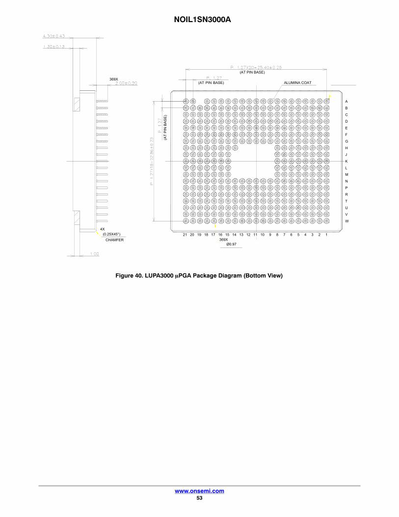
NOIL1SN3000A
www.onsemi.com53
Figure 40. LUPA3000 PGA Package Diagram (Bottom View)
ALUMINA COAT
W
V
U
T
R
P
N
M
L
K
J
H
G
F
E
D
C
B
A
123456789101112131415161718192021
369X
Ø0.97
369X
CHAMFER
(0.25X45°)
4X
(AT PIN BASE)
(AT PIN BASE)
(AT
PIN
BA
SE
)
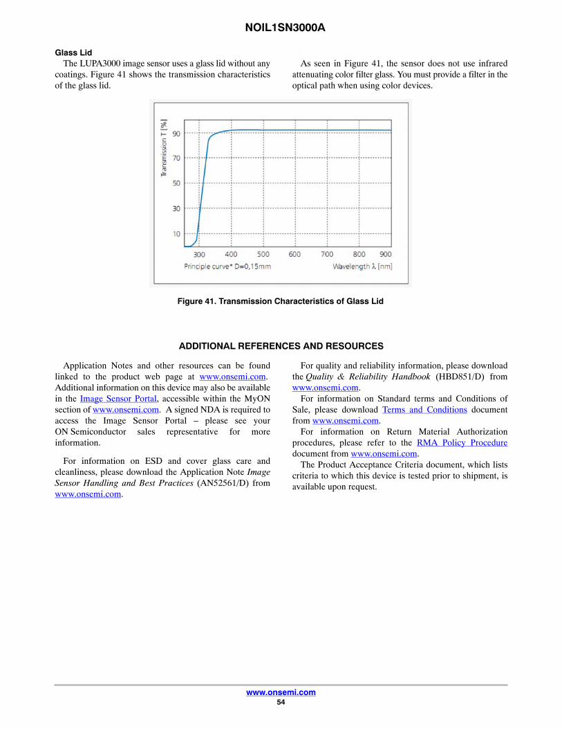
NOIL1SN3000A
www.onsemi.com54
Glass LidThe LUPA3000 image sensor uses a glass lid without any
coatings. Figure 41 shows the transmission characteristicsof the glass lid.
As seen in Figure 41, the sensor does not use infraredattenuating color filter glass. You must provide a filter in theoptical path when using color devices.
Figure 41. Transmission Characteristics of Glass Lid
ADDITIONAL REFERENCES AND RESOURCES
Application Notes and other resources can be foundlinked to the product web page at www.onsemi.com. Additional information on this device may also be availablein the Image Sensor Portal, accessible within the MyONsection of www.onsemi.com. A signed NDA is required toaccess the Image Sensor Portal – please see yourON Semiconductor sales representative for moreinformation.
For information on ESD and cover glass care andcleanliness, please download the Application Note ImageSensor Handling and Best Practices (AN52561/D) fromwww.onsemi.com.
For quality and reliability information, please downloadthe Quality & Reliability Handbook (HBD851/D) fromwww.onsemi.com.
For information on Standard terms and Conditions ofSale, please download Terms and Conditions documentfrom www.onsemi.com.
For information on Return Material Authorizationprocedures, please refer to the RMA Policy Proceduredocument from www.onsemi.com.
The Product Acceptance Criteria document, which listscriteria to which this device is tested prior to shipment, isavailable upon request.

NOIL1SN3000A
www.onsemi.com55
ACRONYMS
Acronym Description
ADC analog-to-digital converter
AFE analog front end
ANSI American National Standards Institute
BGA ball grid array
BL black pixel data
CDM Charged Device Model
CDS correlated double sampling
CIS CMOS image sensor
CMOS complementary metal oxide semiconductor
CMY cyan magenta yellow
CRC cyclic redundancy check
DAC digital-to-analog converter
DDR double data rate
DFT design for test
DNL differential nonlinearity
DSNU dark signal nonuniformity
EIA Electronic Industries Alliance
EOL end of line
ESD electrostatic discharge
FE frame end
FF fill factor
FOT frame overhead time
FPN fixed pattern noise
FPS frames per second
FS frame start
HBM Human Body Model
HMUX horizontal multiplexer
I2C inter-integrated circuit
IEEE Institute of Electrical and Electronics Engineers
IMG regular pixel data
Acronym Description
INL integral nonlinearity
IP intellectual property
JTAG Joint Test Action Group
LE line end
LS line start
LSB least significant bit
LVDS low-voltage differential signaling
MBS mixed boundary scan
MSB most significant bit
MTF modulation transfer function
NIR near infrared
PGA programmable gain amplifier
PLS parasitic light sensitivity
PRBS pseudo-random binary sequence
PRNU pixel random nonuniformity
QE quantum efficiency
RGB red green blue
RMS root mean square
ROI region of interest
ROT row overhead time
S/H sample and hold
SNR signal-to-noise ratio
SOF start of frame
SOL start of line
SPI serial peripheral interface
TAP test access port
TBD to be determined
TIA Telecommunications Industry Association
TR training pattern
uPGA micro pin grid array

NOIL1SN3000A
www.onsemi.com56
GLOSSARY
blooming The leakage of charge from a saturated pixel into neighboring pixels.
camera gain constant A constant that converts the number of electrons collected by a pixel into digital output (in DN). It can beextracted from photon transfer curves.
column noise Variation of column mean signal strengths. The human eye is sensitive to line patterns so this noise isanalyzed separately.
conversion gain A constant that converts the number of electrons collected by a pixel into the voltage swing of the pixel.Conversion gain = q/C where q is the charge of an electron (1.602E 19 Coulomb) and C is the capacitanceof the photodiode or sense node.
CDS Correlated double sampling. This is a method for sampling a pixel where the pixel voltage after reset issampled and subtracted from the voltage after exposure to light.
CFA Color filter array. The materials deposited on top of pixels that selectively transmit color.
color crosstalk The leakage of signal from one color channel into another when the imager is NOT saturated. The signalcan leak through either optical means, in which a photon enters a pixel of the wrong color, or electricalmeans, in which a charge carrier generated within one pixel diffuses into a neighboring pixel.
CRA Chief ray angle. Oblique rays that pass through the center of a lens system aperture stop. Color filter ar-ray, metal, and micro lens shifts are determined by the chief ray angle of the optical system. In general,optical systems with smaller CRA are desired to minimize color artifacts
DN Digital number. The number of bits (8, 12, 14, …) should also be specified.
DNL Differential nonlinearity (for ADCs)
DSNU Dark signal nonuniformity. This parameter characterizes the degree of nonuniformity in dark leakage cur-rents, which can be a major source of fixed pattern noise.
fill-factor A parameter that characterizes the optically active percentage of a pixel. In theory, it is the ratio of theactual QE of a pixel divided by the QE of a photodiode of equal area. In practice, it is never measured.
grating monochromator An instrument that produces a monochromatic beam of light. It typically consists of a broadband lightsource such as a tungsten lamp and a diffraction grating for selecting a particular wavelength.
INL Integral nonlinearity (for ADCs)
luminance Light flux per unit area in photometric units (lux)
IR Infrared. IR light has wavelengths in the approximate range 750 nm to 1 mm.
irradiance Light flux per unit area in radiometric units (W/m2)
Lag The persistence of signal after pixel reset when the irradiance changes from high to low values. In a videostream, lag appears as ‘ghost’ images that persist for one or more frames.
Lux Photometric unit of luminance (at 550 nm, 1 lux = 1 lumen/m2 = 1/683 W/m2)
NIR Near Infrared. NIR is part of the infrared portion of the spectrum and has wavelengths in the approximaterange 750 nm to 1400 nm.
pixel noise Variation of pixel signals within a region of interest (ROI). The ROI typically is a rectangular portion of thepixel array and may be limited to a single color plane.
photometric units Units for light measurement that take into account human physiology.
photon transfer Measurement in which a bare imager (no external lens) is irradiated with uniform light from dark to satura-tion levels. Typically the source is collimated, monochromatic 550 nm light. Chapter 2 of J. Janesick’sbook, Scientific Charge Coupled Devices, describes the technique in detail.
PLS Parasitic light sensitivity. Parasitic discharge of sampled information in pixels that have storage nodes.
PRNU Photo-response nonuniformity. This parameter characterizes the spread in response of pixels, which is asource of FPN under illumination.
QE Quantum efficiency. This parameter characterizes the effectiveness of a pixel in capturing photons andconverting them into electrons. It is photon wavelength and pixel color dependent.
radiometric units Units for light measurement based on physics.
read noise Noise associated with all circuitry that measures and converts the voltage on a sense node or photodiodeinto an output signal.
reset The process by which a pixel photodiode or sense node is cleared of electrons. Soft reset occurs when thereset transistor is operated below the threshold. Hard reset occurs when the reset transistor is operatedabove threshold.

NOIL1SN3000A
www.onsemi.com57
reset noise Noise due to variation in the reset level of a pixel. In 3T pixel designs, this noise has a component (in unitsof volts) proportionality constant depending on how the pixel is reset (such as hard and soft). In 4T pixeldesigns, reset noise can be removed with CDS.
responsivity The standard measure of photodiode performance (regardless of whether it is in an imager or not). Unitsare typically A/W and are dependent on the incident light wavelength. Note that responsivity and sensitivityare used interchangeably in image sensor characterization literature so it is best to check the units.
reverse saturation Phenomenon in which the signal level decreases with increasing light intensity. It typically occurs at irradi-ance levels much higher than saturation, such as an image taken of the sun.
ROI Region of interest. The area within a pixel array chosen to characterize noise, signal, crosstalk, and so on.The ROI can be the entire array or a small subsection; it can be confined to a single color plane.
row noise Variation of row mean signal strengths. The human eye is sensitive to line patterns, so this noise is ana-lyzed separately.
sense node In 4T pixel designs, a capacitor used to convert charge into voltage. In 3T pixel designs it is the photodi-ode itself.
sensitivity A measure of pixel performance that characterizes the rise of the photodiode or sense node signal in Voltsupon illumination with light. Units are typically V/(W/m2)/sec and are dependent on the incident light wave-length. Sensitivity measurements are often taken with 550 nm incident light. At this wavelength, 1 683 lux= 1 W/m2; the units of sensitivity are quoted in V/lux/sec. Note that responsivity and sensitivity are usedinterchangeably in image sensor characterization literature so it is best to check the units.
shot noise Noise that arises from measurements of discretised quanta (electrons or photons). It follows a Poissondistribution with the strength of the noise increasing as the square root of the signal.
spectral response The photon wavelength dependence of sensitivity or responsivity.
SNR Signal-to-noise ratio. This number characterizes the ratio of the fundamental signal to the noise spectrumup to half the Nyquist frequency.
temporal noise Noise that varies from frame to frame. In a video stream, temporal noise is visible as twinkling pixels.
tint Integration time.
ON Semiconductor and are trademarks of Semiconductor Components Industries, LLC dba ON Semiconductor or its subsidiaries in the United States and/or other countries.ON Semiconductor owns the rights to a number of patents, trademarks, copyrights, trade secrets, and other intellectual property. A listing of ON Semiconductor’s product/patentcoverage may be accessed at www.onsemi.com/site/pdf/Patent−Marking.pdf. ON Semiconductor reserves the right to make changes without further notice to any products herein.ON Semiconductor makes no warranty, representation or guarantee regarding the suitability of its products for any particular purpose, nor does ON Semiconductor assume any liabilityarising out of the application or use of any product or circuit, and specifically disclaims any and all liability, including without limitation special, consequential or incidental damages.Buyer is responsible for its products and applications using ON Semiconductor products, including compliance with all laws, regulations and safety requirements or standards,regardless of any support or applications information provided by ON Semiconductor. “Typical” parameters which may be provided in ON Semiconductor data sheets and/orspecifications can and do vary in different applications and actual performance may vary over time. All operating parameters, including “Typicals” must be validated for each customerapplication by customer’s technical experts. ON Semiconductor does not convey any license under its patent rights nor the rights of others. ON Semiconductor products are notdesigned, intended, or authorized for use as a critical component in life support systems or any FDA Class 3 medical devices or medical devices with a same or similar classificationin a foreign jurisdiction or any devices intended for implantation in the human body. Should Buyer purchase or use ON Semiconductor products for any such unintended or unauthorizedapplication, Buyer shall indemnify and hold ON Semiconductor and its officers, employees, subsidiaries, affiliates, and distributors harmless against all claims, costs, damages, andexpenses, and reasonable attorney fees arising out of, directly or indirectly, any claim of personal injury or death associated with such unintended or unauthorized use, even if suchclaim alleges that ON Semiconductor was negligent regarding the design or manufacture of the part. ON Semiconductor is an Equal Opportunity/Affirmative Action Employer. Thisliterature is subject to all applicable copyright laws and is not for resale in any manner.
PUBLICATION ORDERING INFORMATIONN. American Technical Support: 800−282−9855 Toll FreeUSA/Canada
Europe, Middle East and Africa Technical Support:Phone: 421 33 790 2910
Japan Customer Focus CenterPhone: 81−3−5817−1050
NOIL1SN3000A/D
LITERATURE FULFILLMENT:Literature Distribution Center for ON Semiconductor19521 E. 32nd Pkwy, Aurora, Colorado 80011 USAPhone: 303−675−2175 or 800−344−3860 Toll Free USA/CanadaFax: 303−675−2176 or 800−344−3867 Toll Free USA/CanadaEmail: [email protected]
ON Semiconductor Website: www.onsemi.com
Order Literature: http://www.onsemi.com/orderlit
For additional information, please contact your localSales Representative
◊

Mouser Electronics
Authorized Distributor
Click to View Pricing, Inventory, Delivery & Lifecycle Information: ON Semiconductor:
NOIL1SN3000A-GDC NOIL1SE3000A-GDC