non-intrusive data aquisition system - open...
TRANSCRIPT

NON-INTRUSIVE DATA AQUISITION SYSTEM
Item Type text; Proceedings
Authors Moore, Willard; Grahame, Bill
Publisher International Foundation for Telemetering
Journal International Telemetering Conference Proceedings
Rights Copyright © International Foundation for Telemetering
Download date 14/05/2018 09:30:38
Link to Item http://hdl.handle.net/10150/615707

NON-INTRUSIVE DATA AQUISITION SYSTEM
Willard Moore Bill Grahame
Design EngineersLoral Data Systems
San Diego, Calif.
ABSTRACT
Previous solid rocket motor instrumentation was inadequate to correlate motorperformance with analysis. This is particularly obvious when flight failures occur. Theaddition of instrumentation, both externally and internally, to the rocket motor has helpedsolve this problem. External instrumentation has been implemented quite easily withexisting technology. However, internal instrumentation has been very difficult toimplement. This has been mainly due to the complexity of breaching the motor case. Asystem was developed that transmits power through the case structure to a uniqueencoder/signal conditioner which then transmits the data back across the case structure foranalysis. This was accomplished by magnetic coupling avoiding any disruption of the casestructure. A detailed discussion of the magnetic coupling, signal conditioning and encodingfunctions will be presented.
INTRODUCTION
In the history of solid rocket motor flights, a number of unresolved failures have occurred.These failures went unresolved because they either could not be correlated with staticmotor firing performance data, or could not be diagnosed at all due to inadequate flightinstrumentation data. A program was therefore developed to greatly increase theinstrumentation on flight rocket motors.
Under this program, a portion of the instrumentation was designed to be placed inside therocket motor between the case and the insulation. The purpose of this instrumentation wasto measure such key motor design verification parameters as temperature, heat flow, andpropellant stresses during motor burn. A major problem with this system was developing asafe, reliable means of routing power and signal through the motor case to these internalsensors. Drilling holes though the case would cause severe stresses and possible leakpaths. Winding wires through the layers of Kevlar during motor fabrication would causestresses an potential wire breakage. Even routing wires through the normal closures in the

case had potential for wire breakage and high stresses at the closures. And since largequantities of sensors (up to 64) were considered, any hardwired scheme would have toallow for the routing of hundreds of wires to flight signal conditioning/data acquisitionequipment via missile-level cabling.
One solution to this problem was to develop a system capable of routing power and signalsthrough the motor case without the use of wires. This system would consist of (at least)two parts: An internal unit, which would be located inside the motor case in the sameplane as the sensors; and an external unit, which would be located directly across themotor case from the internal unit. The internal unit would contain a power receivingsection, an encoder section and a signal transmitting section. It would have to be small,extremely low-profiled, and contoured to fit the shape of the motor case. It would have towithstand pressures in excess of 1000 psi. All wiring to the sensors would have to beterminated at the unit without any gaps on stress risers.
An external unit would house a power coupling and data receiving section. The unit wouldalso be rigid, light weight, and would contour to the motor case. The power couplersection would have to be very efficient and provide minimal interference to the signalcircuitry.
This paper presents the design of a non-intrusive data acquisition system which wasdeveloped to meet these requirements.
This system was developed and delivered under contract to United Technologies ChemicalSystems Division San Jose, Calif. The system was designed for use on the Trident II D5third stage rocket motor development system.
SYSTEM DESCRIPTION
External System
As shown in figure 1, the external system receives the DC (28±6V) power from the rocketmotor power source, converts it to a square wave for coupling across the case structureand generates the voltages required to operate the data coupler detector and the outputbuffer.
The received bi-phase level (BI0/-L) data stream from the internal unit is applied todifferential line drivers capable of driving greater than 500 feet of twisted shielded paircable.

Internal System
The internal system (see figure 2) derives its power from the external system via the powercoupler. System voltages are created from the square wave coupled across the casestructure. These system voltages are used for proper system operation and sensorexcitation sources. The output of the sensors are conditioned as necessary, prior to routingto the Pulse Code Modulation (PCM) encoder. The PCM encoder accepts 64 differentialchannels of sensor data, amplifies where necessary, and converts the analog to its binaryequivalent. The converted data are then merged with a frame sync code to form a serialnon-return-to-zero (NRZ-L) data stream. This data stream is converted to BI0/-L andcoupled across the case structure for further processing by the external unit.
The PCM encoder is a fixed format encoder utilizing CMOS circuits to reduce the powerconsumption. The format and the programmable gain amplifier are controlled by a CMOSPROM for versatility.
Programmable Gain Amplifier (PGA) Multiplexer
The Analog Multiplexer section accepts 64 differential inputs (see figure 3). The datasignals are sequentially sent to the inputs of a differential programmable gaininstrumentation amplifier (PGA) via Metal Oxide Semiconductor Field Effect Transistor(MOSFET) gates. The PGA amplifier output is applied to the input of a summing amplifierthat functions as a thermocouple reference compensation circuit.
All input data are sampled by one of the eight monolithic 16 channel multiplexers that arecombined to form the 64 differential inputs. These devices are constructed with acomplementary MOS process with inputs protected from overvoltages exceeding eithersupply. Protection is provided against damage from overvoltages up to ±33V.
When addressed, the input data are routed to the PGA amplifier inputs. The monolithicamplifier used in this application is a controlled gain block, which features differentialinputs (single ended output) and an accurate I/O gain relationship. As a completeamplification circuit, this device does not depend on external resistor matching for I/Oisolation. It has a high Common Mode Rejection Ratio (100db) in any application. Theamplifier gain is set by the ratio of resistors selected to provide the programmable gains.The four discrete gains are 500, 100, 50 and 1. The gain of one is used for the two internalchannel monitors, scaled temperature and supply voltage.
The temperature of the internal unit is sensed by a thermocouple and scaled by an amplifiercircuit (discussed with the signal conditioning) to provide the compensation signal(temperature information). This signal is summed with the thermocouple channels at the

appropriate time by the analog switch. At all other times the summing amplifier receives azero signal.
Analog-to-Digital (A/D) Format Control
The serial pulse amplitude modulated data stream (analog data) from the summingamplifier is encoded to its binary equivalent form by a sample and hold circuit andsuccessive approximation A/D converter (see figure 4) prior to interleaving in the NRZ-Ldata stream. The sample and hold circuit samples the data for one word time period, thenholds the data sample during its conversion to binary form during the next word period.The circuit accomplishes this function by charging a high quality polycarbonate capacitorto the sampled value, then switching the capacitor to a high input impedance bufferamplifier where the value is held until the conversion is complete.
The parallel data from the A/D converter are loaded into a parallel-to-serial shift registerfor conversion to serial form. The serial output is routed to a digital multiplexer forinsertion into the serial NRZ-L data stream. This NRZ-L data stream is later converted toBI0/-L format for transmission.
The format control generates the timing signals required to select, convert, and format aninput signal. The timing signals are based on CLK (a 50% duty cycle signal whose periodis one bit time) and CT (a signal whose period is one word time, eight bits).
A CMOS programmable read only memory (PROM) is used to generate the gain controlsignal, the analog/sync select signal and the end of frame pulse. The PROM is apolysilicon fuseable link with byte-wide organization. The PROM address inputs comefrom a binary counter, operated at the system word rate.
Frame sync code is generated by two CMOS edge triggered parallel to serial shiftregisters. The sync code (1110101110010000) is loaded into the registers at the beginningof every frame to provide frame synchronization.
The basic system timing is established by a crystal oscillator circuit utilizing a CMOS hexinverter, a crystal, and an appropriate drive circuit, to form a simple yet highly reliablereference oscillator. This circuit provides a bit rate stability of 0.1%.
Signal Conditioning
The signal conditioning supplied for this application consisted of a multiplexed constantcurrent supply for stress tranducers and shear gage excitations and thermocouple referencejunction compensation and termination.

Current Source Excitation
Figure 5 is a schematic of the basic constant current circuit that was used to supply theconstant current requirements. The formula for determining the load current IL, is:
R3*VrefIL = -----------
R1*R5
Output current adjustment (if required) is accomplished by changing the value of one ofthe R1 resistors. The circuit as shown will yield a current variation of less than 0.5% overthe operating temperature range. Of course, any change in the value of Vref will have adirect effect on the output current. To reduce the effect this variation has on systemoperation, the Vref input is the reference for the A/D converter and as such any drift in theconstant current caused by the reference will tend to be cancelled.
Also contained in figure 5 is the functional schematic of the pulse current excitation circuit(PCE). Unlike classical methods of continuous bridge excitation, the PCE suppliesexcitation current only to the bridge being sampled by the PCM encoder. The PCM formatcontrol determines which analog multiplexer channel will be selected. Current is routedthrough the selected analog multiplexer to the sensor for one word period. This time periodallows for the excitation current to settle before the PCM encoder samples the model ofthe sensor circuitry. As indicated the current pulse is completely stable in 45 nsec. This issignificantly less than the word time of 16 usec.
Thermocouple Termination
Since every pair of dissimilar metals in contact constitutes a thermocouple (includingcopper/solder) and since a useful electrical circuit will contain at least two contacts inseries, measurements with thermocouples must be implemented in a manner whichminimizes undesired contributions of incidental thermocouples and provide a suitablereference.
Thermocouple compensation techniques include physical references (ice-point cells),ambient temperature reference junctions and the electronic cold-junction compensators.The most suitable form for this application is cold junction compensation, primarily due tothe physical problems. The thermocouples (see figure 7) are terminated at an iso-thermalblock and the temperature of the block is measured by a suitable device. The temperaturemeasuring device chosen for this application is the Analog Devices AD590 temperaturesensor. This device outputs a current that is directly proportional to the temperature. The

ouptut current is then scaled and used to compensate for the iso-thermal blocktemperature.
Due to extremely small volume constraints and the location where it would be used,standard isothermal blocks for thermocouple termination were not deemed practical. Thechromelalumel thermocouples were soldered (using high temperature silver solder) directlyto the internal unit printed circuit board. After testing the unit was potted solid with anepoxy base material. When cured this material provided the unit with a homogenousstructure that forms the required isothermal block. The AD590 temperature sensor wasmounted to the printed circuit board in the same location as the terminated thermocouples.Thus, the sensor maintains the same temperature as the thermocouples.
Power and Signal Coupling
The couplers must transfer energy to the internal electronics and transducers while alsoreceiving the acquired data from the internal electronics.
Field Choice
The primary decision to be made was which force field, electric or magnetic, should beemployed. In considering the electric field case, a coupler could be designed using a set ofparallel plate capacitors and a oscillating current generator. The current generator wouldbe connected to two electrodes and the electric field would induce current to the internalside for power. A similiar approach would be used for the signal coupler. The initialanalysis indicated the external volts required would be extremely high due to the inherentlow capacitance of such a system.
As previously indicated, the magnetic field was selected for the power and signal couplers.
Core Geometry
The magnetic field caused by a flowing current is controlled by the geometry of the currentcarrying conductor. When the current carrying conductor is formed into the proper shape,a magnetic field penetrates into the internal side of the coupler and is transformed back toa flowing current. Choice of coupler geometry is made by trading-off efficiency with thephysical space available. The height contraint of 0.25"-0.30 ruled out the use of severalgeometries. Toroidal, pot core and C-cores were determined to be unuseable with thisheight restraint.
The geometry for the power and signal coupler was chosen to be the disc core. Thisgeometry is shown in figure 8a and 8b. A disc core with windings external to the core

represents a short cylindrical solenoid. Figure 8c is a photograph of the actual magneticfield shown by the orientation of iron filings. Along the vertical center of figure 8a, the fluxwill be perpendicular to the flat face of the core, toward either edge of the core the fluxwill diverge outward. Not all the flux generated by the primary will reach the secondary;however windings can be added without increasing the height of the core to achieve therequired voltage at the secondary.
The general shape of the magnetic field of figure 8a will result regardless of thepermeability of the core material. However, the presence of magnetic material increasesflux density due to the reduced magnetic path length.
Power Coupler
The applied unregulated voltage in the range of 28V passes through a reverse polarityprotection diode (see figure 9) and EMI filter to a power switch controlled by a pulsewidth modulator circuit. The EMI filter is a Pi type consisting of an input capacitor, seriesinductor and output capacitor.
The pulse width modulator (PWM2) operates at a fixed pulse width and less than 50%duty cycle to ensure that there will be no destructive simultaneous conduction in the drivertransistors. Storage times in the driver transistors ranged from 1 to 2 usec. If driver 2 getsturned on before driver 1 has completely turned off, there would be a destructive currentspike in driver 2 due to the primary voltage coupling of the transformer. Since themagnetic coupling from primary to secondary is less than perfect, because of the relativelylarge air gap, the collapsing magnetic field each half cycle will cause a voltage spike as thefield cuts through primary windings. This voltage spike must be clamped to a safe level toprevent secondary breakdown. Ultra-fast recovery diodes are used as voltage clamps whiledriver transistors rated at 150 volts permit safe operation.
Signal Coupler
The geometry used for the signal coupler is similar but smaller than the geometry for thepower coupler since the power handling requirements are significantly less. Figure 10 is ablock diagram of the signal coupler.
The input to the signal coupler is encoded as BI0/-L. This code ensures that there will be noDC content in the transmitted signal. The reason DC content can not be permitted is thatover time the primary of the signal transformer will saturate. It would be the same asapplying a non-zero DC voltage to the primary. Eventually the core would “walk up” thehysteresis loop and one of the drivers would try to switch a low impedance to the supplydrawing excessive current. Although the transistors used for the signal coupler are much

faster than those used in the power coupler (which thay have to be since the frequency ismuch higher) they still have some storage time. The use of a blanking pulse generatormakes sure that for this period of time, drive is removed from both transistors. On theexternal side are two damping resistors critically damping the parallel resonant circuitformed by the secondary inductance and its own ditributed capacitance. The high inputimpedance of the comparator will not sufficiently damp this circuit alone. Finally, a highspeed comparator transforms the received singal back to TTL levels.
Physical Considerations
Figure 8c shows a photograph of an actual magnetic field from a magnetic coupler primarycarrying a current of 4 amperes. It is clear that at the edges of the core the field becomesquite circular, and the changing field could induce an EMF in an adjacent coil of wire (oretch). This is exactly what occurred in the first unit. Due to the very small sizerequirements a large separation between the coupler and input circuitry was not possible.Since the primary power coupler generates stronger fields than the secondary due to highercurrent, shielding is more critical on the internal side. However, in order to preventpenetration of the power coupler field into the signal coupler windings causing data errors,high permeability Mu metal shields were placed over both cores. This technique forces thefield remaining from the power coupler to follow the contour of the Mu metal shieldinstead of traversing laterally into the signal coupler. A Mu metal shield was also used inthe internal unit to help prevent the power coupler signal from entering the high gainamplifier inputs. The output data showed a predominant frequency content at the powercoupler switching frequency. Since this frequency is substantially higher than any expecteddata, standard data reduction techniques (averaging was used) easily removed this error.Future designs will incorporate larger area cores in the internal unit (this reduces fringing)and greater separation between inputs and couplers.
Mechanical Description
The surface mount (primarily flat packs) packaging concept for the system was selected toprovide optimum structural integrity in the dynamic environments while allowing heatdissipation and compliance with the specification requirement for minimum size.
External Unit
The external equipment (see figure 11) consists of a single printed circuit board pottedsolidly into a 6061-T6 aluminum chassis. The potting compound is a one part generalpurpose epoxy manufactured by Emerson & Cuming, Inc. This potting compound providesa homogenous thermal path for power dissipation in the switching transistors. Also, apotted unit is easier to shape to the desired curvature of the case structure.

As indicated, the external unit was required to fit the curvature of a 16 inch diameterrocket motor case while maintaining as low a profile as possible. The height for thisdiameter case was 0.762 inches. A single 15-pin connector was provided for theapplication of power and extraction of data. The flanges on each end of the unit were usedto secure the unit to the outside of the rocket motor case.
Internal Unit
One of the most challenging aspects of the project was the packaging of the internal unit.This unit had to conform to the curvature of the case, and in addition to the interestingshape, a number of other requirements had to be met. These requirements includedthermal, pressure, water immersion, acceleration, vibration and shock.
Figure 12 is an outline drawing of the internal unit. The flat cables exiting both sides of theunit are the sensor inputs/sensor excitation. All surfaces of the internal unit are designed topresent as smooth a transition as possible to prevent voids form being formed when theunit is installed in the rocket motor. When installed in the rocket motor the unit iscompletely surrounded with an insulating material that serves to protect the unit from theburning fuel. This insulation also causes the internal temperature of the unit to rise since agood thermal path is not available for heat transfer. This condition dictated the design of avery low power unit (the internal requirement was approximately 2 watts).
Considering the thermal shock of 300 deg F for 4 days, a pressure requirement of 1077 psi.(testing indicated many IC packages can’t withstand this pressure), complete immersion insea water and the other operating conditions it was determined that a solid potted unitwould be required to meet the specifications.
Due to the extreme curvature of the motor case a flexible printed circuit board wasrequired. The board was formed prior to component installation and held in the correctshape by a potting fixture. Figure 13 shows a cross section of the unit in the potting mold.The shape of the flexible circuit board can be seen with the power coupler installed. Theeight screws shown are used to position the coupler and printed wiring board prior topotting. The position of the coupler within the unit is critical since any variation in the coredepth (inside the internal unit) will cause a corresponding loss in coupling efficiency.
After significant preliminary testing the unit was placed in the mold for potting. The initialunit that was potted did not function properly. This was later determined to be due toincorrect procedures during the potting process causing the printed wiring board to bedamaged. This was corrected in the mold and testing during the potting process wasimplemented. These changes resulted in units being successfully potted.

Testing of the units was accomplished with internal/external pairs separated with aninsulator to simulate the case. Both internal and external units present special testingproblems once potted solid, since each unit requires the coupling of power and/or signal tooperate properly.
CONCLUSION
A system has been designed, developed and produced that will allow the acquisition ofdata in the hostile environment of a rocket motor The system utilizes magnetic coupling toavoid violating the physical integrity of the case structure. Low power, small size and non-intrusive acquisition methods make this a truly unique telemetry system.
ACKNOWLEDGEMENTS
The authors wish to thank Mr. Glen Campagna of United Technologies Corporation for hisinvaluable contributions to this paper and his considerable time and effort contributedduring the project.


FIGURE 3PGA MULTIPLEXER

FIGURE 4A/D FORMAT CONTROL

FIGURE 5CURRENT EXCITATION SOURCE

FIGURE 6STEP RESPONSE
OF CURRENT SOURCE
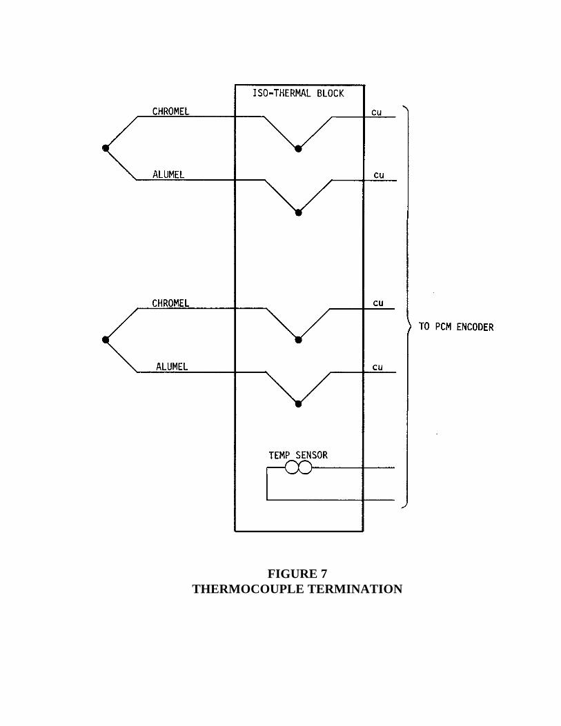
FIGURE 7THERMOCOUPLE TERMINATION

FIGURE 8A
FIGURE 8B
FIGURE 8C
FIGURE 8CORE GEOMETRY

FIGURE 9POWER COUPLER

FIGURE 10SIGNAL COUPLER

FIGURE 11OUTLINE DRAWING
EXTERNAL UNIT

FIGURE 12OUTLINE DRAWING
INTERNAL UNIT
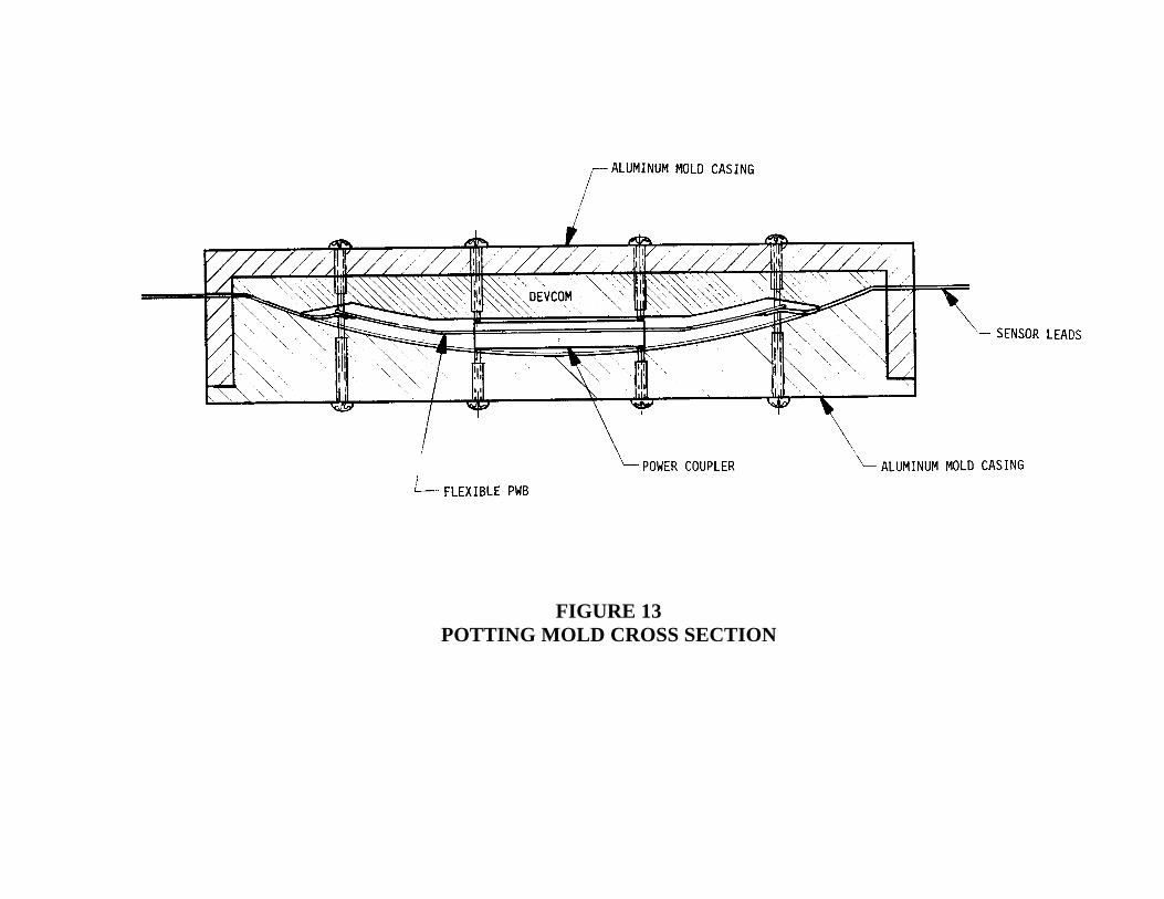
FIGURE 13POTTING MOLD CROSS SECTION