northwestern university x-ray structural analysis of in
TRANSCRIPT

NORTHWESTERN UNIVERSITY
X-ray Structural Analysis of In-Situ
Polynucleotide Surface Adsorption and Metal-
Phosphonate Multilayer Film Self-Assembly
A DISSERTATION
SUBMITTED TO THE GRADUATE SCHOOL IN PARTIAL FULLFILLMENT OF THE REQUIREMENTS
for the degree
DOCTOR OF PHILOSOPHY
Field of Materials Science and Engineering
By
Joseph Anthony Libera
EVANSTON, ILLINOIS
JUNE 2005

ii
© Copyright by Joseph A. Libera 2005
All Rights Reserved
iii
ABSTRACT
X-ray Structural Analysis of In-Situ Polynucleotide Surface
Adsorption and Metal-Phosphonate Multilayer Film Self-Assembly
Joseph Anthony Libera
The X-ray Standing Wave (XSW) analytical technique was adapted to
measure nano-scale structures in the 0.5 – 50 nm length range using large d-
spacing layered synthetic microstructure (LSM) X-ray mirrors. This allowed for the
first ever use of multiple orders of Bragg reflection in long-period XSW analysis.
XSW analysis was combined with X-ray reflectivity (XRR) and X-ray fluorescence
(XRF) to analyze layer-by-layer assembly of metal-phosphonate multilayer films as a
test case and to measure for the first time the in-situ process of adsorption of
polynucleotides and counterions to charged planar surfaces. The surface chemistry
was built on the outermost silica surfaces of 19-22 nm d-spacing Si/Mo LSMs. XSW
experiments were conducted by simultaneously collecting X-ray reflectivity and X-ray
fluorescence data in continuous θ-2θ scans from the total external reflection (TER)
region through four or five orders of Bragg reflection.
Multilayer metal phosphonate thin films were prepared via a layer-by-layer
assembly process using the metallic ions Zr4+, Y3+, Hf4+, and phosphonate molecules
1,12-dodecanediylbis(phosphonic acid) (DDBPA), porphyrin bis(phosphonic acid)
(PBPA) and porphyrin square bis(phosphonic acid) (PSBPA). An initial study of PBPA
and PSBPA using Y, Hf and Zr led to the optimized design of DDBPA and PSBPA films
using Zr and Hf only prepared in 1, 2, 3, 4, 6, and 8 layer series on both Si(001)
substrates for XRR and on 18.6 nm period Si/Mo LSMs for XSW.

iv
Positively and negatively charged surfaces were prepared for the in-situ study
of the adsorption of Zn2+ and Hg-poly(U). Hydroxyl-terminated surfaces were used to
examine the adsorption of Hg-poly(U) to like charged surfaces using Zn2+
counterion-mediated adsorption. The measurements were performed in a liquid-solid
interface (LSI) cell using aqueous solutions of Hg-poly(U) and ZnCl2. Using 50 µM
ZnCl2 alone, adsorption of Zn2+ was observed to the hydroxyl terminated surface.
When 25 µM Hg-poly(U) and 50 µM ZnCl2 were used, a time-dependent adsorption
was observed with no initial absorption of either Zn or Hg-poly(U) followed by Zn
adsorption and then Hg-poly(U) adsorption.
Approved:
Professor Michael J. Bedzyk
Department of Materials Science and Engineering
Northwestern University
Evanston, IL

v
ACKNOWLEDGEMENTS
Thank you to all those who have helped me during my PhD pursuits. Special
thanks to Duane Goodner who showed me how to operate the X15A beamline and to
Dr. Kai Zhang for getting me started in polyelectrolyte adsorption experiments.
Special thanks to Prof. Monica Olvera and Hao Cheng for their assistance in the
preparation in Hg-poly(U) and theoretical interpretation of the XSW adsorption
observations. Thanks to my fellow group members Anthony Escuadro, Drs. John
Okasinski, Chang-Yong Kim, Don Walko, Zhan Zhang and Hua Jin for their assistance
in synchrotron experiments. Special thanks to Dr. Chian Liu for manufacturing the
excellent LSM X-ray mirrors. Thanks to Dr. Rich Gurney and Craig Schwartz for their
assistance in the preparation of metal phosphonate sample films. Thanks to Drs.
Zhong Zhong (BNL), John Quintana and Denis Keane (DND-CAT/APS), and Tien-Lin
Lee (ESRF) for there assistance in synchrotron experiments. I would also like to
thank Prof. Sonbinh Nguyen and Prof. Joseph Hupp for their collaboration in the
metal phosphonate film study. I would like to thank Prof. Kenneth Shull, Prof.
Alfonso Mondragon and Professor Monica Olvera de la Cruz for serving on my thesis
defense committee.
I owe a great debt of gratitude to Prof. Michael Bedzyk who taught me the
very exciting XSW method and showed me how to do good science in general. I am
especially grateful for the flexibility and patience he has shown towards me.
Lastly, I would like to thank my father-in-law, Dr. Martin Harrow, for his
tireless encouragement and advice and my wife Jean and children Natasha, Daniel
and Laura for there support and patience while I asked them to endure extra
hardship that allowed me to pursue my doctorate.

vi
TABLE OF CONTENTS
LIST OF TABLES ix
LIST OF FIGURES x
Chapter 1 Introduction 1
Chapter 2 Theory and Modeling Details for Long-Period XSW Analysis 6
2.1 Introduction 6
2.2 Theoretical Treatment 11
2.2.1 Multilayer Recursion Formulation 11
2.2.2 Implementation of the Recursion Formula 14
2.2.3 The SUGOM XSW Data Processing Graphical User Interface 15
2.3 Reflectivity Modeling and E-Field Intensity Computation 16
2.4 Atomic Distribution Modeling 24
Chapter 3 Experimental Details 25
3.1. X-ray Setups 25
3.1.1 NSLS X15A Experimental Setup 25
3.1.2. ESRF ID32 Experimental Setup 27
3.1.3 APS 5BMD Experimental Setup 28
3.1.4. NU X-ray Lab Experimental Setup 29
3.2. Data Collection and Processing 29
3.2.1. SUGOM – Experimental Yield Reduction GUI 29
3.2.2 X-ray Fluorescence Emission Sensitivity Factor Calculation 32
3.3 Liquid-Solid Interface Cell 33
3.4. Sample Preparation 36
3.4.1. LSM Substrate Fabrication 36
Chapter 4 XSW Study of Metal Phosphonate Multilayer Thin Films 39
4.1 Introduction 39
4.1.1 Early Work in Metal-Phosphonate Thin Films 40

vii
4.1.2 Recent Work 43
4.2 Experimental Strategy and Sample Preparation 43
4.2.1 Sample Preparation 48
4.3 Results and Discussion of Metal-Phosphonate Films 49
4.3.1 XRR and XRF Results and Discussion of Samples A-D 50
4.3.2 XSW Results and Discussion of Samples A1 and A8 54
4.3.3 XRR and XRF Measurements F- and H-series 64
4.3.4 XSW Results for G- and I-series 65
4.3.5 Discussion for the F-, G-, H-, and I-series 94
4.3.6 Primer Layer Characterization 99
4.3.7 Metal Phosphonate Coordination Chemistry 101
4.3.8 Performance of the Large d-Spacing LSMs 102
4.4 Conclusions 106
Chapter 5 Hg-poly(U) Adsorption to Charged Surfaces 108
5.1 Introduction 108
5.1.1 DNA Condensation in Bulk Solution 109
5.1.2 Adsorption of Polyelectrolytes to Positively Charged Surfaces 112
5.1.3 Adsorption of Polyelectrolytes to Negatively Charged Surfaces 113
5.1.4 Strategy for In-Situ Measurement of Hg-poly(U) Adsorption 114
5.1.5 Charging Behavior of the Planar SiO2 Surface 117
5.2 Experimental Details 118
5.2.1 Mercuration of Polyuridylic Acid 118
5.2.2 Sample Preparation 119
5.2.3 Ex-situ XSW Measurements 121
5.2.4 In-situ XSW Measurements 121
5.3 Ex-Situ XSW Hg-poly(U) Adsorption Results 122
5.3.1 Adsorption of Hg-poly(U) to an Amine-Terminated Surface 122
5.3.2 Adsorption of Hg-poly(U) to a Zr-Terminated Surface 125
5.4 In-Situ XSW Zn and Hg-poly(U) Adsorption Results 128
5.4.1 In-situ Adsorption of Zn2+ to an OH Surface 131
5.4.2 Zn2+ Adsorption to a PO3 Surface 134
5.4.3 Hg-poly(U) Adsorption to an OH Surface 136
5.4.4 Miscellaneous Results from other In-Situ Experiments 145

viii
5.5 Discussion 147
5.5.1 Zn Adsorption to a PO3 Terminated Surface 147
5.5.2 Zn Adsorption to an OH Terminated Surface 148
5.5.3 Adsorption of Hg-poly(U)/Zn to an OH Terminated Surface 149
5.6 Conclusions 154
Chapter 6 Summary and Future Work 156
6.1 Thesis Summary 156
6.2 Future Work 158
REFERENCES 160
Appendix A Software Documentation for SUGOM XSW Analysis Program 170

ix
LIST OF TABLES
Table 4.1 XRR and XRF results of sample films C and D 52
Table 4.2 Results from XRR and XRF analysis for the F- and H-series 68
Table 4.3 XSW and XRF results for the G- and I-series samples 73
Table 5.1 XSW model parameters for the in-situ adsorption 143
Table 5.2 XSW ICP_AES analysis results 145
Table 5.3 Results from miscellaneous additional experiments 146

x
LIST OF FIGURES
Figure 2.1 Conceptual diagram of the XSW principle 7
Figure 2.2 Comparison of grazing angle XSW methods 9
Figure 2.3 Simple model fit for the 15 layer-pair Si/Mo LSM 17
Figure 2.4 LSM model fit with graded d-spacing 18
Figure 2.5 Final LSM model fit with graded interfaces 19
Figure 2.6 Comparison of the 18.6 and 21.6 nm LSM designs 23
Figure 3.1 Experimental setup at the NSLS X15A beamline 26
Figure 3.2 Screen shot of the SUGOM graphical user interface program 30
Figure 3.3 Liquid-Solid Interface cell 34
Figure 4.1 Effect of incubation time on Zr/phosphonate layer thickness 41
Figure 4.2 Molecular diagrams of phosphonate molecules 44
Figure 4.3 Layer structure of sample film A8 45
Figure 4.4 Structural diagrams of metal-phosphonate films 46
Figure 4.5 XRR results of sample films C and D 51
Figure 4.6 Sample A8 XSW results 55
Figure 4.7 Electron density profile for sample film A8 56
Figure 4.8 Surface plot of the calculated E-field intensity 57
Figure 4.9 Sample A1 XSW results 62
Figure 4.10 Perspective diagram of porphyrin square molecules 63
Figure 4.11 XRR results of F-Series films 66
Figure 4.12 XRR results of H-Series films 67
Figure 4.13 XRR results for F- and H-series films 69
Figure 4.14 XRR of I2 film from XSW scan 71

xi
Figure 4.15 Typical MCA spectrum for I-series films 72
Figure 4.16 XSW results for film G1 74
Figure 4.17 XSW results for film G2 75
Figure 4.18 XSW results for film G3 76
Figure 4.19 XSW results for film G4 77
Figure 4.20 XSW results for film G6 78
Figure 4.21 XSW results for film G8 79
Figure 4.22 G-series XSW Hf results 80
Figure 4.23 G-series XSW Zr results 81
Figure 4.24 XSW results for film I1 83
Figure 4.25 XSW results for film I2 84
Figure 4.26 XSW results for film I3 85
Figure 4.27 XSW results for film I4 86
Figure 4.28 XSW results for film I6 87
Figure 4.29 XSW results for film I8 88
Figure 4.30 I-series XSW Hf results 89
Figure 4.31 I-series XSW Zn/Re results 90
Figure 4.32 I-series XSW Zr results 91
Figure 4.33 Modeled atomic heights for G- and I-series 92
Figure 4.34 Atomic coverage of the F-I series films 93
Figure 4.35 Primer Layer Structure 100
Figure 4.36 Alternate models comparison for film I8 103
Figure 4.37 Sensitivity of model to layered vs single slab 104
Figure 4.38 Sensitivity of LSM to sense layered structure 105
Figure 5.1 Spermine concentrations versus DNA concentration 110

xii
Figure 5.2 Adsorption phase diagram of polyelectrolyte chains 111
Figure 5.3 AFM image of adsorption of DNA to DPDAP 113
Figure 5.4 Schematic diagram of Zn2+ mediated Hg-poly(U) adsorption 115
Figure 5.5: MCA Spectrum for Sample A1b 123
Figure 5.6: XSW Results for Sample A1b 124
Figure 5.7: MCA Spectrum for Sample B1a 126
Figure 5.8 XSW results for sample B1a 127
Figure 5.9 Modeling details of in-situ reflectivity 129
Figure 5.10: MCA Spectrum for Sample JL817BOH_A 132
Figure 5.11: In-situ XSW result for 50 mM ZnCl2 placed in contact with an OH
terminated LSM/SiO2 substrate. 133
Figure 5.12: Adsorption of Zn to a PO3 surface 135
Figure 5.13: MCA Spectrum for Sample JL817OH_A 137
Figure 5.14: Hg-poly(U)/Zn Adsorption Time Sequence 138
Figure 5.15: Results from the XSW scan 53 from sample JL817OH_A 139
Figure 5.16: Results from the XSW scan 54 from sample JL817OH_A 140
Figure 5.17: Results from the XSW scan 55 from sample JL817OH_A 141
Figure 5.18: Condensed layer coverages of Zn and Hg as a function of time 142
Figure 5.19: Calculated adsorption for sample JL817OH_A 151
Figure 5.20: Calculated surface charge for sample JL817OH_A 152
Figure 5.21: Calculated divalent metal ion coverage for sample JL817OH_A 153

1
Chapter 1: Introduction
Nano-engineering is an emerging area scientifically important to both the
electronic and biomolecular industries. In order to understand the behavior of
structures as their dimensions approach the nanoscale, better characterization tools
are a continuing need for today’s scientific and technological communities. While
many important characterization tools such as scanning probe microscopy, electron
microscopy and numerous spectroscopic methods have been adapted or were
already well suited for nano-scale objects, additional tools are always welcome. In
this thesis the extension of X-ray Standing Wave (XSW) analysis to nanoscale
objects is described. The applicability of XSW analysis to nanoscale objects was
improved by the development of large d-spacing layered-synthetic-microstructure
(LSM) X-ray mirrors whose long-period XSWs provide a probe well suited for
characterizing the structure of 0.5-50 nm sized objects. This new extension of the
XSW technique was used to analyze the structure of metal phosphonate layer-by-
layer assembled thin films and for the in-situ study of the polynucleotide adsorption
to charged surfaces.
Layer-by-layer assembled mono- and multi-layer thins films are most
commonly assembled onto SiO2 or Au substrates whose surfaces are not atomically
flat[1]. In these films, the surface over-layers are typically not in registry with the
crystallographic planes of an underlying single crystal so that conventional single
crystal XSW analysis is not applicable. Even if atomic registry was present, the large
period of the multilayer films, typically 1-2 nm in this thesis, requires longer period

2
XSWs to determine their structure. In the structural characterization of thin films,
the following properties are of interest: (a) chemical structure, (b) atomic or
molecular density, (c) thickness and position of each layer in the film, (d) uniformity
and size of lateral domains. Functional properties such as photoluminescence,
dielectric behavior, porosity, magnetism, electrochemical, and catalytic behavior are
aggregate properties which are often closely related to the structural properties. The
commonly used characterization techniques are ellipsometry, scanned probe
microscopy, and a variety of spectroscopic techniques [2]. In certain instances
sufficient ordering exists to allow scanned probe microscopy to resolve ordered
domains and the lateral variation thereof. Other less commonly used techniques are
X-ray photoelectron spectroscopy for the determination of chemical bonding states
and quantification of atomic coverage and various spectroscopic tools (ATR FTIR,
SPR, and Raman) to determine various properties that are related to atomic vibration
states or electronic transitions. Small angle X-ray scattering methods such as X-ray
reflectivity (XRR) and grazing incidence diffraction (GIXRD) are less frequently used
methods that provide structural information in the surface normal and lateral
dimensions, respectively.
XSW analysis is a highly specialized technique that permits both the atomic
distribution and absolute amount of the atoms or molecules within the distribution to
be measured[3]. The atomic positions are determined with respect to the X-ray
reflecting planes of the substrate. In the most common variety of XSW analysis, the
atomic positions are determined with respect to a perfect single crystal lattice. A
limitation of any variation of the XSW technique is that the unknown structures
should be of the same length scale as the period of the XSW in order to determine

3
both the position and width of the distribution. Since the period of the XSW is
nominally the crystallographic spacing of the X-ray mirror, a synthetic crystal with a
much larger d-spacing can be designed with the appropriate length scale for the
problem of interest. These synthetic crystals are called layered synthetic
microstructures (LSMs) consisting of alternating layers of high and low electron
density materials and have been in common use for many years as X-ray and UV
optics components[4-8] and as substrates for XSW analysis[9-13]. Previous XSW
work however, has incorporated LSMs with relatively small d-spacing (less than 8
nm) and utilized only 1st order Bragg reflection since the higher orders of Bragg
reflection were too weak. In this thesis the range of applicability of LSMs is expanded
by making very large d-spacing LSMs (18.6-21.6 nm) which provide many orders of
Bragg reflection permitting the simultaneous probing of distributions of medium (~
0.5 nm) and large (~ 50 nm) length scales. The lower limit of this range is
determined at the same time by the attainable degree of perfection of the LSM and
by the surface roughness of the LSM onto which sample films are constructed. For
example, an LSM that provides a 0.2 nm period XSW is of little use if the over-layer
sample structures are superposed onto a high (~0.5 nm) surface roughness
topography. The XSW period upper level of 50 nm is achieved in the TER low-angle
condition. Samples in this thesis were only up to 20 nm in height. Thicker over-
layers present a coupled problem in which the XSW within the sample films depend
strongly on the films themselves especially at the lower angles but the coupling can
be easily handled using a self-consistent modeling procedure. Experimentally, the
efficiency of the XSW technique depends on the emission rate of X-ray fluorescence
and the efficiency in which these can be collected. In general, the higher energy X-

4
ray lines of the higher atomic weight atoms (Z ~ 20 or higher) provide the most
efficient XSW measurements.
An excellent thin-film system for study by XSW is metal-phosphonate layer-
by-layer assembled thin-film architecture. Metal-phosphonate films are ideally suited
for study by XSW because they contain metal atoms in layers parallel to the
substrate or LSM surface. In addition, several metals can be used interchangeably,
namely Hf, and Zr so that one or the other can be used in a single layer to mark a
specific location in a multilayer film. In general, thin films do not necessarily contain
the heavy atoms required to provide a strong X-ray fluorescence signal. For such
cases similar thin films must be made that incorporate heavy atoms as fluorescent
markers.
Many systems of biological relevance can be easily made accessible to XSW
techniques by attaching suitable heavy-atom markers, such as Se, Br, or Hg, to the
biological objects of interest. Further advantage from the XSW technique is made
possible by in-situ experimentation which is not available in many other methods. In
this thesis the adsorption behavior of Hg-labeled polyuridylic acid (Hg-poly(U)) to a
negatively charged surface using Zn2+ aqua ions is examined. The simultaneous
measurement of the position and concentration of both the counterion and
biomolecular polyion has never been attempted before and development of this
technique will provide highly sought after data for the verification of theoretical
treatment of the adsorption process.
This thesis presents the first use of long-period XSW using multiple orders of
Bragg reflections from large d-spacing LSMs. The structural analysis of metal-
phosphonate layer-by-layer assembled thin films and in-situ biomolecular adsorption

5
whose structural dimensions are in the 0.5-20 nm length scale is demonstrated. In
Chapter 2 the theoretical basis for XSW analysis is summarized with emphasis on the
special needs arising from the use of large d-spacing LSM X-ray mirrors. In Chapter
3 the details of the experimental setups are provided. In Chapter 4, an XSW
structural analysis of a variety of metal-phosphonate layer-by-layer assembled thin
films is presented. These films are based on the metal atoms Zr, Hf, Y, Zn, and Re
and the metal phosphonate molecules 1,12-dodecanediylbis(phosphonic acid),
porphyrin bis(phosphonic acid) and porphyrin square bis(phosphonic acid). In
Chapter 5 the study of the adsorption of Hg-poly(U) and Zn to a hydroxyl terminated
SiO2 surface is presented. The study is performed using a liquid-solid interface (LSI)
cell providing in-situ analysis of the adsorption of Zn and mercurated long-chain
polyuridylic acid (poly(U)) from aqueous solution. The XSW analysis of adsorption
from Zn-only aqueous solution to hydroxyl and phosphate terminated surfaces is also
presented. In addition, an ex-situ XSW analysis of adsorption of Hg-poly(U) to
positively charged surfaces is presented. In Chapter 6 a summary of this thesis work
is given along with recommendations for future work. Appendix A provides detailed
documentation for the MATLAB computer programs developed as part of this thesis.

Chapter 2: Theory and Modeling Details for Long-Period XSW Analysis 2.1 Introduction
X-ray standing wave (XSW) analysis is an established method for determining
surface over-layer atom distributions with respect to the substrate diffraction planes.
The technique has been successfully applied to a variety of systems ranging from
sub-angstrom adsorbate position determination with respect to crystal lattices [14,
15] to locating atomic layers in surface over-layers 100 nm above an x-ray mirror
surface using total external reflection x-ray standing waves TER-XSW [16]. The
method has also been successfully applied to the study of in-situ ion adsorption to
planar substrates from liquids [10, 12, 17, 18]. In all cases the basic principle of
standing wave analysis is straightforward. An x-ray standing wave is created when
an incoming x-ray plane wave interferes with the outgoing x-ray plane wave after
being reflected from an x-ray mirror as shown in Figure 2.1. At any given angle of
incidence the XSW field consists of planes of equal electric-field (E-field) intensity
perpendicular to the scattering vector, oR kkqvvv −= . As the angle of incidence (θ) is
varied, both the phase and amplitude of the sinusoidal E-field intensity vary to
produce a very useful characteristic modulation in the x-ray fluorescence emission
from heavy atoms located in layers parallel to planes of equal intensity of the E-field.
The various ways of reflecting x-rays lead to variations in the XSW method: (a)
total-external reflection (TER) [12, 16, 19] (b) dynamical Bragg diffraction from
6

7
...
Mo
Mo
Mo
Si
Si
Si
SiO2
k0 kR
1
3
2
Mo
Si NBL = 20
Si
z I(z)
ρ(z)
kR
k0
q
d
2θ
...
Mo
Mo
Mo
Si
Si
Si
SiO2
k0 kR
1
3
2
Mo
Si NBL = 20
Si
z I(z)
ρ(z)
kR
k0
q
d
2θ
Figure 2.1: Simple model for the NBL=20 layer-pair Si/Mo LSM used in this thesis
and a conceptual diagram of the XSW principle. The simplified LSM picture here
does not show the graded d-spacing or Nevot-Croce interfacial structure used in
the detailed models (see text and Figure 2.5. The inset in the upper right shows
the E-field variation (light line) in the q-direction for a particular angle theta. The
atomic distribution (heavy line) is shown centered on an anti-node position which
will produce a minimum XSW fluorescence yield from the atoms

8
perfect crystal lattices[14, 15, 17, 20, 21] and (c) Bragg diffraction from layered
synthetic microstructures (LSMs) [10-13]. The period of the standing wave in a
vacuum generated by x-rays of wavelength λ, is D = λ/(2 sin θ), where 2θ is the
angle between the incident ( okv
) and reflected ( Rkv
) wave vectors. As the incident
angle is scanned across a Bragg peak, the phase of the XSW shifts inward by π
radians, effectively scanning the XSW nodes in the qv− direction. When a
distribution of atoms ρ(z) is confined to a layer whose thickness is of the same
magnitude as the period of the XSW, then a X-ray fluorescence modulation will be
produced as the nodal planes pass through the layer. This modulation is a Fourier
component of the atomic distribution and contains information about the position and
width of the layer.
Recent advances in single crystal XSW have shown that by using many
orders of Bragg reflections, a mathematical Fourier inversion technique can be used
to reconstruct the 3-dimensional atomic distribution relative to the underlying perfect
crystal lattice [22, 23]. In this method each XSW measurement at a Bragg reflection
provides a single Fourier component of the unknown atomic distribution. If enough
Fourier components can be measured, then Fourier inversion can be performed to
obtain a model independent determination of the atomic distribution. For the present
case of surface over-layers, the atomic distribution varies in a single dimension only
but the process of Fourier inversion is applicable as well.
Previous long-period XSW studies at grazing angles of incidence have only
utilized TER [12, 16, 18, 19] or TER plus a single LSM Bragg peak[11,13]. In Figure
2.2 we show for comparison the reflectivity for these previous studies along with the

9
(b) TER + 1st LSMBragg peak
(a) TER (high electron density Au mirror)
(d) Large d-spacing LSMwith ideal interfaces
(c) Large d-spacing LSMused in this thesis
(b) TER + 1st LSMBragg peak
(a) TER (high electron density Au mirror)
(d) Large d-spacing LSMwith ideal interfaces
(c) Large d-spacing LSMused in this thesis
Figure 2.2: Comparison of grazing angle XSW methods. Calculated X-ray specular
reflectivity vs. scattering vector magnitude for different X-ray mirror designs. (a)
Au mirror (b) 200 layer-pair Si/W LSM with d = 2.5 nm and tSi = 0.75d (c) 20
layer-pair Si/Mo LSM with d = 18.6 nm and tSi = 0.86d (d) same as (c) but with tSi
= 0.9d and ideal layers (sharp interfaces and uniform d-spacing)

10
reflectivity for LSMs from this thesis. In Figure 2.2a we show the reflectivity resulting
from a simple Au mirror [16]. The high optical density provides an extended TER
region making Au an ideal substrate for studying narrow distributions as high as 100
nm above the Au surface. In Figure 2.2b we show the reflectivity for a 200-layer pair
Si/W LSM x-ray mirror with a 2.5 nm LSM period as used in Ref.[11]. For this case
both TER and the single Bragg peak were used to probe structure within Langmuir-
Blodgett films and where the Bragg peak together with the TER region were able to
remove the modulo-d ambiguity that exists if just the TER XSW modulation is used.
However, this also requires that the atomic distribution profile be narrow enough to
produce a modulation in the 2.5 nm period XSW resulting from the 1st Bragg peak.
The LSMs used in this thesis overcome this limitation by using a large d-spacing LSM
as shown in Figure 2.2c. The bilayer period d and Si/Mo thickness ratio were
adjusted to provide high reflectivity Bragg peaks over as large a range in q as
possible. In Figure 2.2c the calculated reflectivity of LSMs used in this thesis is
shown which very closely fits the measured reflectivity (see below Fig. 2.5). In
Figure 2.2d an ideal Si/Mo LSM is shown which is not realized due to imperfections in
the manufacturing process. This calculation demonstrates the potential of large d-
spacing LSMs to provide many orders of Bragg reflection over a very large range in
q. Improvements in LSM manufacture will be desirable to obtain the many Fourier
component needed for a direct-methods Fourier inversion technique. It will also be
important to obtain a very high LSM surface quality since high order Bragg reflection
with a 2-3 nm d-spacing will only be useful if the surface over-layers are sufficiently
parallel and narrow with respect to the XSW period of the highest order Bragg peak.
The interfacial roughness inside the LSM, surface roughness and subsequent

11
parallelism of the surface overlayers each need to be maintained within tolerances
dictated by the smallest period XSW under consideration. In this thesis the XSW
analysis uses model-dependent determination of atomic distribution profiles in
several systems of interest which provides valuable experience for the future use of
LSM’s for use as direct methods probes.
2.2 Theoretical Treatment
2.2.1 Multilayer Recursion Formulation
The theoretical basis for predicting x-ray standing wave phenomena is based
on Parratt’s recursion formulation[24] which applies Maxwell’s equation to the
system described in Figure 2.1 which models an X-ray multilayer mirror by a series
of N layers with thickness dm and indices of refraction nm = 1 – δm – iβm. Detailed
and complete derivations have been documented in previous PhD work[25, 26] and
journal publications[27, 28].
Below we present a summary derivation for the calculation of the x-ray
reflectivity and E-field intensity based on the MS and PhD thesis work of
Bommarito[25] which is used for the theoretical prediction of the experimentally
measured x-ray reflectivity and x-ray fluorescence yield respectively. The E-field
amplitudes of the incident and reflected x-ray plane waves in the mth layer are
expressed as:
[ ]
[ ])rkt(iexp)0(E)r(E
)rkt(iexp)0(E)r(E
Rm
Rmm
Rm
mmmm
vvv
vvv
⋅−ω=
⋅−ω= (2.1)

12
By applying the interface boundary conditions that require continuity of the
tangential components of the electric and magnetic fields and invoking Snell's law
the following recursive formulation for predicting the reflectivity from any interface in
the layered model system is derived,
[ ][ ])dfk2(iexpRF1
)dfk2(iexpRFR
mm11m,mR
m,1m
mm11m,mR
m,1mm,1m −⋅+
−+=
+−
+−− (2.2)
where
m1m
m1mR
ffffF
m,1m +−
=−
−−
(2.3)
is the Fresnel coefficient and where mm21m i22f β−δ−θ= which follows from Snell’s
law and uses the small angle approximation θ = sinθ. The incident wave vector
k1 = 2π/λ where λ is the x-ray wavelength in air. In Equation 2.2 and 2.3, the
complex quantities Fm,m-1 and fm are determined by model parameters (dm, δm, and
βm) and can be easily calculated for each value of the incident angle θ = θ1. The
recursive calculation begins with the infinitely thick bottom layer (m=N) where there
is only a transmitted and no reflected beam; and therefore the reflectivity is zero.
Therefore with the substrate as the Nth layer we have,
0R 1N,N =+ (2.4)
The topmost layer (m = 1) of the system is an air or vacuum layer and the recursive
relation Equation 2.2 is repeated until R1,2 is found which is the observable x-ray
reflectivity of the system. The formulation to this point is all that is needed to
compute the reflectivity R experimentally observed in the X-ray Reflectivity (XRR)
measurements presented in this thesis.

13
In order to proceed to x-ray standing wave analysis, we must next compute
the E-field in the layers in which the unknown atomic distribution resides. We start
with the definition of the reflectivity coefficient,
)()(
1,mm
mRm
mm dEdER =+ (2.5)
to obtain the E-field amplitudes at the interface of layer m. For XSW calculations we
need the E-field intensity I(q,z), for each angle θ of the experiment and for all
interior positions z in the layer m over which the unknown atomic distribution is
assumed to reside. After lengthy derivation we obtain,
[ ])zAk2cos(R2)zBk4exp(R1)zBk2exp()0(E
)z(I
mm1Rm1m,mmm1
21m,mmm1
2m
mm
′−φ+′−+−
=
++
(2.6)
Where and . In the present nomenclature, Ennn zdz −=′ )arg( 1, += mmRm Rφ m(0) and
Em(dm) refers to the transmitted E-field amplitude at the top and bottom of the mth
layer respectively and Em(z) is thus the E-field amplitude at a location z below the
top of the mth layer. Em(0) is the transmitted E-field amplitude at the m-1,m
interface and is computed using a recursion formula for the transmission coefficient
similar to Equation 2.2. The terms Am and Bm were defined as follows:
2221
21 4)2()2(
21
mmmmA βδθδθ +−+−= (2.7)
2221
21 4)2()2(
21
mmmmB βδθδθ +−+−−= (2.8)

14
2.2.2 Implementation of the Recursion Formula.
In order to analyze the XSW data, it was necessary to develop computer
algorithms for computing the reflectivity, R(θ), E-field intensity, I(θ,z) and X-ray
fluorescence yield, Y(θ). The algorithms were implemented in a number of computing
functions written in the MATLAB technical computing environment which are
documented in Appendix A. The most important MATLAB function is called
xswan2b.m and computes the reflectivity and E-field intensity for a given incident
angle θ and position z in layer m. This function is the starting point of the XSW
analysis and is based on the Fortran program xswan.f from a previous PhD work[25].
Many new MATLAB functions were developed for the modeling of reflectivity and x-
ray fluorescence yield. The most important of these are functions that create layered
models from a set of input parameters which was required in order to implement
least squares regression analysis.
For the theoretical modeling of reflectivity data, we use the xswan2b.m
function. We begin with an assumed layered model of the system and adjust the
unknown model parameters using least squares regression analysis until a
satisfactory prediction of the experimental reflectivity is obtained. Once this is
complete, the calculation of the E-field intensity follows by repeatedly invoking
xswan2b.m over a suitable θi, zi computational grid. Normally we choose θi to match
the experimental data and for zi we choose an appropriate grid density that will
provide sufficient point density in the geometric scale of the assumed atomic
distribution profiles. A typical computational 2D grid had 600 steps in θ and 800
steps in z. In order to permit the calculation of atomic distribution repeatedly for
many atomic profiles and several atoms, the E-field intensity, I(θi,zi), is saved to a

15
computer file for later retrieval. This is done to avoid repeating the lengthy
computation over the 600 x 800 computational grid each time a yield curve is
calculated. Once we have computed and stored the E-field intensity I(θ,z), modeling
of the measured fluorescence yield proceeds by assuming a functional form for the
unknown atomic distribution. For example, the most common functional form is the
Gaussian profile centered at z0 with Gaussian width σ. The theoretical fluorescence
yield is then calculated using the following integral,
∫ −= dzezIzYield z αµθρθ sin/),()()( (2.9)
where ρ(z) is the unknown atomic distribution. The attenuation factor in the
integrand accounts for the attenuation of the outgoing fluorescent X-rays. This is an
important factor when the fluorescence originates from within the LSM and the
fluorescence detector takeoff angle (α) is small or when Kapton and water films are
used. Normally, the attenuation term is taken outside the integral since this term is
essentially constant for typical atomic distributions ρ(z). Optimization is done by
using a least squares minimization of the parameters of the atomic distribution
model ρ(z).
2.2.3 The SUGOM XSW Data Processing Graphical User Interface.
Also written were MATLAB functions and a graphical user interface (GUI)
program for computation of normalized fluorescence yield and reflectivity from
experimental XSW data. This MATLAB GUI named SUGOM.m, is a successor to the
Macintosh Fortran programs SUGO and parts of SWAN. The functionality of SUGOM
includes (a) parsing of the raw XSW 2D data files (XRF MCA channels and reflectivity

16
vs. angle θ), (b) peak fitting of the x-ray fluorescence spectra at each angle step to
extract the total fluorescence counts from the atoms of interest, (c) automatic
normalization for XRF detector dead-time effects and incident photon intensity and
(d) calculate the measured normalized specular reflectivity. SUGOM.m was an
essential requirement due to the very large single scan files (600 steps) that could
not be handled easily using the original SUGO program.
2.3 Reflectivity Modeling and E-Field Intensity Computation
In order to precisely model the fluorescence yield, the E-field intensity, I(θ,z)
must be accurately predicted. The validity of the I(θ,z) prediction is premised on the
successful prediction of the observed reflectivity. A layered model was used for the
LSM which included a sample film. In this thesis samples are prepared as over-layers
on (a) bare Si substrates or (b) NBL = 15 or 20 Si/Mo LSM substrates. A layered
model is used to represent both LSM and surface over-layers except where the
surface over-layers are monolayers coverages of atoms in which case they are not
included. A layered model consists of a list of N layers in which we specify the index
of refraction nm = 1 - δm - iβm, the layer thickness dm and an optional Debye-Waller
type interface roughness σm. The 1st layer in the model is a vacuum layer and the
final or Nth layer is the Si substrate whose thickness is set high enough to guarantee
the zero-reflectivity premise. In the case of the 15-layer pair Si/Mo LSM, the
simplest possible model consists of (a) vacuum layer, (b) 15 pairs of Si/Mo bi-layers
and (c) Si substrate layer for a total of 32 layers. In Figures 2.3 to 2.5 a comparison
of successive model improvements used to model the LSM portion of the system is

17
q (Å-1)
Ref
lect
ivity
δ x
105
e-de
nsity
ρe
(e-/A
3 )
Depth z (nm)
graded d-spacing = 0%σSi/Mo = 0 nm
Si Mo Si
(a)
(b)
q (Å-1)
Ref
lect
ivity
δ x
105
e-de
nsity
ρe
(e-/A
3 )
Depth z (nm)
graded d-spacing = 0%σSi/Mo = 0 nm
Si Mo Si
(a)
(b)
Figure 2.3: Simple model fit for the 15 layer-pair Si/Mo LSM used in the X15A
experiments. The model uses ideally sharp interfaces and a uniform d-spacing. (a)
Predicted (solid line) and measured (open circles) x-ray reflectivity. (b) electron
density profile (graphical equivalent of the layered model). Only the 1st full LSM
period is shown. The surface roughness, σS, has no noticeable effect on R.

18
q (Å-1)
Ref
lect
ivity
δ x
105
e-de
nsity
ρe
(e-/A
3 )
Depth z (nm)
graded d-spacing = 2.5%σSi/Mo = 0 nm
Si Mo Si
(a)
(b)
q (Å-1)
Ref
lect
ivity
δ x
105
e-de
nsity
ρe
(e-/A
3 )
Depth z (nm)
graded d-spacing = 2.5%σSi/Mo = 0 nm
Si Mo Si
(a)
(b)
Figure 2.4: LSM model fit for the 15 layer-pair Si/Mo LSM in Figure 2.3 with the
addition of a 2.5% graded d-spacing. (a) Predicted (solid line) and measured
(open circles) x-ray reflectivity. (b) electron density profile (graphical equivalent
of the layered model). Only the 1st full LSM period is shown.

19
e-de
nsity
ρe
(e-/A
3 )
q (Å-1)
Ref
lect
ivity
δ x
105
Depth z (nm)
graded d-spacing = 2.5%σSi/Mo = 0.30 nm
N = 15d = 216.1(2) nm *tSi/d = .818(4) *2σS = 0.4 nm
*fitting parameters 2 σSiMo 2 σMoSi
2 σSSi Mo Si
2σSiMo = 0.61(2) nm *2σMoSi = 1.22(2) nm *tSiO2 = 2.0 nmρMo = 9.7 g/cm3
(a)
(b)
e-de
nsity
ρe
(e-/A
3 )
q (Å-1)
Ref
lect
ivity
δ x
105
Depth z (nm)
graded d-spacing = 2.5%σSi/Mo = 0.30 nm
N = 15d = 216.1(2) nm *tSi/d = .818(4) *2σS = 0.4 nm
*fitting parameters 2 σSiMo 2 σMoSi
2 σSSi Mo Si
2σSiMo = 0.61(2) nm *2σMoSi = 1.22(2) nm *tSiO2 = 2.0 nmρMo = 9.7 g/cm3
(a)
(b)
Figure 2.5: Final LSM model fit for the 15 layer-pair Si/Mo LSM in Figure 2.3 with
the addition of a 2.5% graded d-spacing and Nevot-Croce interfacial structure. (a)
Predicted (solid line) and measured (open circles) x-ray reflectivity. (b) electron
density profile (graphical equivalent of the layered model). Only the 1st full LSM
period is shown.

20
presented starting with the simplest model having ideal interfaces and a uniform d-
spacing. In Figure 2.3 the best fit to the reflectivity of the NBL=15 LSM using the
simplest model is shown along with the electron density profile. It can be seen that
the simplest model provides a reasonable fit to the experimental reflectivity. Two
additional model features were added to improve the reflectivity fit. In Figures 2.4
and 2.5 the improvement in the predicted reflectivity from the model refinements is
shown. In Figure 2.3, the peak reflectivity at the higher Bragg peaks are over-
predicted which cannot be corrected by implementing a Debye-Waller type
roughness factor without causing a rather poor prediction at the lower order Bragg
peaks. The first model refinement is the use of a graded d-spacing correction to
account for a small decrease in the sputter deposition rate during the manufacture of
the LSMs. A linear decrease of 2.5% from the first layer to the final layer was used.
The resulting incremental improvement is shown in Figure 2.4. The main effect in the
predicted reflectivity is to cause an angle shift of the Bragg peaks relative to the
thickness fringes which primarily is a function of the overall LSM thickness. This shift
affects the peak shape as the thickness fringes superpose asymmetrically as
compared to the simpler model. The correction is most visible in the right flank of
the 3rd Bragg peak in Figures 2.3 and 2.4. Further improvement occurs in the
prediction of the peak heights due to the fact that the graded d-spacing results in a
less perfect periodicity so the superposition of reflected wave fronts from all the
interfaces is lowered. In the second model refinement a Nevot-Croce type treatment
[29] is added to account for the inter-diffusion of Si and Mo at the interfaces. Several
published reports [30-32] providing TEM micrographs have shown the widths of the
interfaces are asymmetric with the Mo on Si interfacial width being about twice the Si

21
on Mo which is a consequence of sputter deposition properties of the heavier Mo
versus Si atoms. The main effect of the Nevot-Croce correction is to reduce the
sharpness of the electron density gradient. In implementing the Nevot-Croce
interfacial profile which is essentially an error function profile, 10 additional layers
were used in the model at each boundary between Si and Mo. Thus the 32 layer
model shown in Figure 2.3 and 2.4 increased to a 332 layer model from the
additional 20 interface layers added for each bilayer of Si/Mo. Although the published
asymmetrical nature of the Mo/Si versus Si/Mo interfaces was implemented here, it
was found that the asymmetry could be implemented in the opposite way to give a
similar improvement. The main effect of this model refinement was reduction of the
electron density gradient. Figure 2.5 show the very good fit resulting from both
additional model features.
After implementing the graded d-spacing and Nevot-Croce interfacial
structure model refinements, one peculiar deviation remains which is the over-
prediction of the height of the first visible thickness fringe on the low-angle flank of
the Bragg peaks. This anomaly is most probably due to a more complex variation of
electron density over the whole LSM structure and was considered too minor warrant
further model refinement. However, throughout this thesis the over-predicted
thickness fringe is almost always present and in most cases is carried over to an
over-predicted XSW thickness fringe modulation. Some experimentation in model
features was attempted and it was found that a simple perturbation of several
percent in the thickness of just one layer (perhaps due to an anomaly in sputter
deposition conditions) resulted in disruption in the regularity of the thickness fringe

22
envelope. Although possibly leading to slight further improvements, the model was
not further refined.
The discussion demonstrating the LSM model used throughout this thesis
referred to 21.6 nm d-spacing LSMs that were used in the first study conducted at
the NSLS X15A beamline. Subsequently, the LSM properties were refined to optimize
them for XSW purpose. To this end the LSM in Figure 2.2d would have been the best
choice but was not attempted because the large interface widths observed in the
21.6 nm LSM suggested that there would have been a complete penetration of Si
from both sides of the Mo layers causing a lowering of the peak optical density that
is provided by a pure Mo layer. Thus the Mo layer was kept to a minimum thickness
of ~2.6 nm to avoid this. The next LSMs were fabricated and the resulting reflectivity
compared in Figure 2.6 to the original 21.6 nm LSM. The main improvement is the
increase in the peak heights of the higher order Bragg peaks. The primary
adjustment parameter is the Si/Mo ratio which affects the Bragg peak at which
extinction in Bragg reflectivity occurs. For example, if the d:Mo thickness ratio is 5:1,
then the 5th Bragg peak will be extinct. Essentially, by choosing a higher value for
the d:Mo ratio, the form-factor envelope that decreases Bragg peak intensity is
extended. One can also see why this parameter is important in predicting higher
order peak intensity. Fortunately, the position of the critical angle and 1st Bragg peak
width are very sensitive to the Si/Mo ratio and so that the conflict in predicting high
order peak reflectivity among the interfacial width, Si/Mo ratio and Mo density is
avoided.
The preceding discussion of LSM modeling has focused primarily on the Si/Mo
layer structure and composition. Consideration of the effects of the oxide of the top

23
(b) A115(Si/Mo)d = 21.6 nm
(a) I320(Si/Mo)d = 18.6 nm
(b) A115(Si/Mo)d = 21.6 nm
(a) I320(Si/Mo)d = 18.6 nm
Figure 2.6: Comparison of the (a) 20 layer-pair Si/Mo LSM used in ESRF ID32
experiments with (b) 15 layer-pair Si/Mo LSM used in NSLS X15A experiments.
The LSM in (a) was an adjusted design following experience gained from using
the LSM in (b). The XSW period, DXSW = 2π/q, in vacuum or air is shown on the
secondary axis on the top.

24
)
Si layer and the sample film over-layers must also be given. The main effect of the Si
oxide layer is to add uncertainty to the absolute position of the top surface of the
LSM with respect to the LSM. The exact value of the oxide layer thickness and
subsequently the total thickness of the oxide plus the remainder of the top Si layer is
very difficult to determine from the specular reflectivity measurements. The oxide is
expected to consume some fraction of the sputter deposited top layer of Si. A value
of 2.0 nm was chosen for the oxide thickness, 1.0 nm of which was subtracted from
the thickness of the top Si so that the final thickness of the top SiO2/Si layer was 1.0
nm thicker. Several samples having monolayer coverage of a heavy atom at the SiO2
surface were consistent with this assumption.
2.4 Atomic Distribution Modeling.
The E-field intensity, I(θ,z), is calculated for a discrete set of values zi and θj,
where i = 1…M and j = 1…N. The values of M and N depend on the measured angular
range and predicted range in z of the unknown atomic distribution ρ(z) as well as the
minimum ∆zi to properly discretize ρ(z). The integral in Equation 2.7 is performed
numerically using the trapezoid rule:
( )[ ]( ii
N
iiijiij zzzzEFIzzEFIYield −+= +
−
=++∑ 1
1
111 2/)(),()(),( ρθρθ (2.8)
The choice of ∆z is made when I(θ,z) is computed. Typically ∆z = 0.05 nm or
greater. Details of the MATLAB computer implementation are provided in Appendix A.

25
Chapter 3: Experimental Details 3.1 X-ray Setups
XSW experiments were performed at the X15A beamline of the National
Synchrotron Light Source (NSLS), Brookhaven National Laboratory and at the ID32
beamline of the European Synchrotron Radiation Facility (ESRF) in Grenoble, France.
XRR experiments were performed at the Northwestern University X-ray Facility using
the 18-kW rotating anode reflectometer. XRF measurements were performed during
XSW measurements and additionally at the 5BMD beamline of the Advanced Photon
Source (APS), Argonne National Laboratory.
3.1.1 NSLS X15A Experimental Setup
A schematic diagram of the X15A experimental setup is shown in Figure 3.1a.
An unconditioned white beam enters the hutch directly from the synchrotron bending
magnet where it is conditioned by a Ge(111) double-crystal monochromator followed
by a 0.05-mm -high by 2-mm-wide slit. Ion chambers before and after the incident
beam defining slit record the full and reduced size beam intensities. The incident
beam flux was 4.0x10⁸ p/s/mm2 at 12.4 keV and 2.0x10⁹ p/s/mm2 at 18.3 keV. The
sample was mounted on a specially designed vertical translation stage shown in
Figure 3.1b which was mounted to a horizontally configured Huber 2-circle
diffractometer. The reflected x-ray intensity was recorded by an ion chamber or
photodiode mounted on the 2θ arm which also had guard and detector slits for

26
X15A Hutch
Ge(111)monochromator
whitebeam
ic0mon
LSM/sample
det
Huber 2-circlediffractometer
Uni
Slid
e
Incident x-ray beam
(b)
(a)
z motion
PGT x-ray detector snout
Side View Schematic (SSD not shown)
X15A Hutch
Ge(111)monochromator
whitebeam
ic0mon
LSM/sample
det
Huber 2-circlediffractometer
Uni
Slid
e
Incident x-ray beam
(b)
(a)
z motion
PGT x-ray detector snout
Side View Schematic (SSD not shown)
Figure 3.1: Experimental setup at NSLS X15A beamline. (a) beamline layout showing
white radiation entering the experiemental hutch from right. (b) custom stage for
providing vertical positioning of sample with respect to the center of rotation or
beam. Shown with a liquid-solid interface cell.

27
shielding stray radiation. An PGT energy dispersive Si(Li) solid-state detector was
used with a Tennelec TC244 spectroscopic amplifier and an Oxford PCA3 computer
board multi-channel-analyzer (MCA) to collect x-ray fluorescence spectra at each
angle step of the scan. A Berkely Nucleonics random pulse generator of constant
average input pulse frequency was used for dead-time correction. A Sr implanted
standard having an RBS calibrated coverage of 10.0 Sr/nm2 was used to determine
the absolute coverages of Hf, Zr, Zn, Re and Hg. At Eγ = 18.3 keV the atomic x-ray
fluorescence sensitivity factors [33] for Zn Kα, Y Kα, Zr Kα, Hf Lα and Re Lα relative
to Sr Kα are 0.330, 1.11, 1.23, 0.352 and 0.497, respectively. A nitrogen gas
purged polypropylene chamber was used to protect the samples from air exposure
during all measurements.
3.1.2. ESRF ID32 Experimental Setup
The ID32 beamline at ESRF has a 0.77 x 0.05 mm2 (HxV) FWHM source size
with a divergence of 0.028 x 0.004 mrad2 (HxV) FWHM with two undulators available
for the production of a high flux (7x10¹⁴ ph s-1 mm-2) beam. The incident beam was
conditioned by a double-crystal Si(111) monochromator which has a cryogenically
cooled first crystal. The second crystal has the ability to focus horizontally but this
feature was not used so the beam size at the diffractometer was V x H = 400x800
µm2 which was reduced in size by a 20-µm -high by 1.0-mm-wide slit so that the full
beam width was used at all times and was reduced in the vertical direction only.
Knife edge scans measured the actual vertical size FWHM to be 15 µm. The incident
flux on the sample was 1.5x10¹¹ p/s at 14.3 keV and 1.8x10¹¹ p/s at 12.4 keV.
Vertical and horizontal positioning of the sample was done by a Huber tower which

28
also provided the θ motion using the phi arc of the Huber tower. The reflectivity and
fluorescence data was simultaneously collected in a θ-2θ (chi-gamma at the ID32
beamline) scan covering the range of TER through the first four Bragg peaks of the
LSM mirrors used in each sample (theta (chi) = 0.0 to 0.6 deg). MCA x-ray
fluorescence spectra were collected at each angle step of the scan using a Canberra
8715ADC multi channel analyzer with a high count-rate RONTEC Si-drift diode solid-
state detector with a 5 mm2 area. The x-ray detector dead-time was measured using
a hardware counter from the Canberra MCA for the input count-rate and using the
totalized MCA spectrum counts for the output count-rate. The dead-time correction
method was verified by taking two scans on the same sample with a small and large
incident beam. A nitrogen gas purged polypropylene chamber was used to protect
the sample from air exposure during all measurements. An As implanted with an RBS
calibrated coverage of 10.4 As/nm2 was used determine atomic coverage of Hf, Zr,
Zn, Re, and Hg. The absolute coverage calculation also required an additional
correction for the fluorescence detector whose detector element is only 300 µm thick
so that the detector efficiency for Zr Kα x-rays is 0.44 compared to 0.99 for Hf Lα
for example.
3.1.3 APS 5BMD Experimental Setup
XRF measurements were performed at the 5BMD bending magnet beamline of
the Advanced Photon Source, Argonne National Laboratory. Incident x-rays of 18.5
keV energy were provided by a Si(111) monochromator. X-ray fluorescence from the
samples was collected using an Ortec IGLET Ge fluorescence detector and an XIA
DXP digital signal processing system which also provides all the necessary data

29
channels for dead-time correction. An ion chamber after the defining slits was used
as the incident x-ray flux monitor. Samples were placed at a glancing angle of θ =
0.5o and fluorescence was collected for 6 minutes. The long counting time was
required due to the relatively low flux of a bending magnet beamline. An As
implanted standard that had an RBS calibrated coverage of 32 As/nm2 was used in
the same geometry to provide a reference atomic coverage. Atomic coverages of the
unknown atoms was determine by referring to the As coverages using calculated
fluorescence emission sensitivity factors[33].
3.1.4. NU X-ray Lab Experimental Setup
Northwestern University X-ray Facility using Cu Kα (8.04 keV) X-rays from a
rotating anode vertical line source coupled to an OSMIC parabolic, graded d-spacing,
collimating, multilayer mirror, followed by a 2-circle diffractometer. The beam size
was 0.10-mm-wide by 10-mm-high. The incident flux was 1x10⁸ p/s. The
instrumental resolution was ∆q = 5x10⁻³ Å-1. The XRR data from the NaI detector
was dead-time corrected and background subtracted.
3.2 Data Collection and Processing
3.2.1. SUGOM – Experimental Yield Reduction GUI
A special requirement created by the use of the large d-spacing LSMs is a way
to handle the very large scan size which was as high as 600 angle steps, each step
having a 512-2048 channel MCA spectrum and as well as all the normal motor angle
and counter data. The predecessor programs which performed the XSW data analysis

30
were the Macintosh Fortran programs SUGO and SWAN. The SUGO program was
used to parse the XSW data files and perform peak fitting of x-ray peaks in the MCA
files and produced individual output files for the net counts in each XRF peak or
counter channel as a function of angle. The SWAN program is used to performed file
arithmetic to calculate the normalized fluorescent yield. It was found to be
advantageous to write an updated data reduction program to handle the larger
number of steps and to integrate the functions of the SUGO and SWAN programs in a
Figure 3.2: Screen shot of the SUGOM graphical user interface program for
analyzing XSW data. The program is written in the MATLAB computing
environment.

31
single program. SUGOM.m was written in the MATLAB computing environment for
this purpose. This program can take arbitrarily large 2D files (600 angle steps x 2048
MCA channel scans was the largest used in this thesis) and automatically perform all
normalization operations including error reporting. Atomic yield curves from as many
as ten x-ray lines can be fit and stored during one fitting operation. The SUGOM
features a graphical user interface to perform file loading, peak fitting and
normalized fluorescence yield output reporting. A screen shot of the SUGOM
graphical interface is shown in Figure 3.3. The main features of the SUGOM program
are:
• A parser to convert SPEC data files into a standard fixed internal data
structure called yield_array. Beamline specific differences in SPEC macro
preferences and detector configurations are written in the parser functions.
The X15A, ESRF, and 5BMD each required a modified parser. At ESRF, the
parser was written in about 4 hours so the task is not too bad after some
practice.
• A file loading program allows the user to navigate to the desired files for
input. The file loader finishes by calling the standard display routines which
display the angle integrated spectrum for all channels collected.
• The peak fitting interface is a user friendly graphical fitting program that
allows initial peak estimates to be made by mouse-clicking on the display and
adjusting the appropriate slider controls. A predefined file of x-ray line labels
is used to associate x-ray peaks with specific atomic lines. A “Prefit Spectrum”
button invokes a free-parameter fit of the initial user guess. The “Calculate
Yields” button invokes the fitting routine for each step in the selected step

32
range after fixing the position and widths of the peaks. Special functions are
built in to SUGOM which allow the user to program special fitting constraints.
For example, the Zn Kβ position, width and height can be specified to be a
function of the Zn Kα peak parameters.
• Once fitting is complete, the “Output Normalized Yields” button writes an
output text file that contains all of the input columns from the parser along
with the computed live-time-fraction, reflectivity, raw and normalized
fluorescence yield. Each output variable is reported along with its error. The
x-ray reflectivity requires user input of the straight through beam detector
and monitor counts input in the SUGOM graphical interface. Another output
feature allows the user to output the current MCA spectrum as a text file.
Several features still not implemented in SUGOM which would be very useful are (a)
the ability to select arbitrary baseline ranges (b) the ability to input channel to
energy calibration values and thus display the x-ray spectrum on an energy axis.
3.2.2 X-ray Fluorescence Emission Sensitivity Factor Calculation. Initially,
the NRLXRF program was used to calculate the relative fluorescent x-ray emission
rates or sensitivity factors. However, it was discovered that this program contains an
error in the calculation of L lines of the heavier elements. For example, Hf Lα is over-
predicted by a factor of 2. Subsequently, the work of Puri et. al. [33] found and used
to compute the sensitivity factors. This recent work provides an updated set of
tabulated x-ray fluorescence cross sections taking into account the most recent
experimental and theoretical developments as of 1995. The tabulated values provide
x-ray fluorescence cross sections for the Ki (i= α,β) for z = 13 to 92 and Lk (k = l, α,

33
β and γ) for z = 35 to 92. The L x-ray cross sections are only tabulated above the L1
edge. The Lα cross sections result from the L1-M4,5 transitions so that the tabulated
values are for the sum of Lα1 and Lα2. The Lβ cross sections result from the L1-M2,3,
L2-M4, L3-N1,4,5, O1,4,5 and P1 transitions so that Lβ is the sum of Lβ1 and Lβ2. Tables
are provided which are essentially lookup tables for the x-ray cross sections as a
function of energy. A logarithmic interpolation procedure is provided for obtaining
intermediate values. In order to calculate the x-ray cross section, σi (i = Kα, Kβ, Ll,
Lα, and Lγ), at intermediate energies, the following interpolation formula is provided,
bii EEEE )/)(()( 22σσ =
where
)log()log(
))(log())(log(
12
12
EEEEb ii
−−
=σσ
The process is a simple one of looking up the values of the cross-section for two
values of E spanning the desired energy and using the above interpolation formula.
3.3. Liquid-Solid Interface Cell
Experiments of ion and bio-molecular adsorption require the use a Liquid-
Solid Interface cell to maintain a liquid contact to the sample surface and at the
same time allow XSW measurement. The design of the LSI cell for experiments in
this thesis was adapted from previous designs made by Dr. Z. Zhang and others
before him. A photograph of the LSI as used in the ESRF ID32 in-situ experiments is
shown in Figure 3.3a and a description of the operation of the cell follows below. The
primary modification of the present cell design is the addition of an o-ring on the
rounded corner of the top face of the cell as the sealing O-ring with the lower o-ring

34
(a)
sampleKapton film
Luer fitting port
sealing o-ringclamp ring
(b)
(a)
sampleKapton film
Luer fitting port
sealing o-ringclamp ring
(b)
Figure 3.3: Liquid-Solid Interface (LSI) cell setup at the ESRF ID32 beamline.(a)
photo showing the LSI cell with Rontec fluorescence detector in the
background.(b) CAD drawing showing the sealing detail of the modified cell
design.

35
serving to stretch the Kapton downward as the Al clamping ring is drawn down by
screws and presses the Kapton to the upper sealing o-ring. The cross-sectional CAD
drawing in Figure 3.3b shows this detail.
Figure 3.3a is a photograph of the liquid-solid interface cell used for the in-
situ XSW measurements. The shell is machined from Vespel™(a polyimide), the x-
ray window on top of the cell is a 7 µm Kapton ™ film sealed by Viton™ o-rings.
Three fluidic ports are used for the injection and withdrawal of test solutions. A N2
filled purge chamber (not shown) with polypropylene windows surrounded the top of
the cell to prevent transport of unwanted CO2 through the slightly permeable Kapton.
The procedure for operating the LSI cell is described below for sample JL817OH_A
which used a solution that was 50µM ZnCl2 and 25 µM Hg-poly(U). The LSI cell is
assembled with a freshly hydroxylated substrate and flushed using 50 ml of Millipore
water that was injected into port A and withdrawn from ports B and C leaving a small
residual volume (~ 0.2 ml). Next, 50 ml of ZnCl2 solution was flushed back and forth
using ports A and B and ejecting a few ml through C. The excess ZnCl2 solution was
withdrawn (leaving ~ 0.2 ml) and valves A, B and C were closed. Next 2-3 ml of Hg-
poly(U)/ZnCl2 solution was injected through port C and a small amount was used to
purge the previous solution past valves A and B. When injected into the LSI cell the
test solution inflates the Kapton film to form a 2 ml reservoir of solution over the
sample surface. The surface was allowed to incubate in this configuration for 60 min.
The solution was then withdrawn back thru Port C and stored for future analysis.
Finally a negative pressure was applied and maintained by withdrawing solution thru
Port A using the 50 µM ZnCl2 syringe. Upon withdrawing the test solution and
applying a negative pressure it took several minutes for the Kapton film to pull down

36
to the sample surface and thus trap a very thin film of test solution (2-3 µm) above
the sample surface. During this process visible light interference fringes could be
seen on the sample surface as the film approached its final thickness, indicating that
the water thickness varied by less than 0.5 µm across the cm lateral extent of the
sample surface. Measurement by XSW followed in the usual way with the X-ray beam
passing through the Kapton and water films establishing the X-ray standing wave in
the test solution above the substrate surface. The water and Kapton layers refract
and partially absorb the incoming and outgoing X-ray beams. This becomes an
increasingly significant effect at small angles.
3.4. Sample Preparation
3.4.1. LSM Substrate Fabrication
Metal/phosphonate mono- and multi-layer films were deposited onto polished
Si (001) wafers or onto specially prepared Si/Mo multilayer x-ray mirrors having SiO2
top surfaces. The Si/Mo x-ray mirror multilayers were prepared by the Optics Group
of the Advanced Photon Source at Argonne National laboratory. The fabrication was
performed using dc magnetron sputtering in a vacuum system pumped by a
turbomolecular pump with a base pressure of low 10-7 Torr. Two 3-in. diameter
sputter guns, 50 cm apart, were deployed facing upward at the bottom side of the
chamber, with uniformity-control masks placed on top of the shield cans. Substrates
were loaded facing downward on a substrate holder on a transport stage. The
transport system is computer controlled and can be synchronized with the sputter
gun power suppliers. The substrates moved linearly over each sputter gun during
deposition, with the gun turned on and off for each layer growth. The thickness of

37
each layer of Mo and Si was controlled by the moving speed and the number of
passes of the substrates over each gun. The sputter guns were set at a constant
current mode, 0.2 A for Mo and 0.5 A for Si, corresponding to a power of ~50 W for
Mo and ~205 W for Si during deposition. The depositions were carried out at
ambient temperatures and at an Ar pressure of 2.3 mTorr.
Si (001) substrates of 2.5 mm x 12.5 mm x 37.5 mm pieces were cut from
pre-polished wafers obtained from Umicore Semiconductor Processing Corp. The
surface roughness of the pre-polished wafers was 0.2-0.5 nm rms. They were
cleaned by piranha etch (2:1 H2SO4:H2O2) at 90oC for 30 minutes followed by
copious rinsing in Millipore water. Fifteen Si/Mo bilayers were deposited on to these
substrates as described above. The bilayer thickness was d=21.6 nm and the
thickness ratio dMo/d was 0.17. The terminating surface of the sputter deposition was
a 17.9 nm thick Si layer which oxidizes in air to provide an SiO2 surface on which
surface functionalization and subsequent metal/phosphonate multilayer growth or
adsorption was done. The final thickness of the top Si/SiO2 layer is different in
general from the Si thickness in any bilayer due to an increase in thickness due to
the oxidation layer.
Due to the small substrate size, the LSM x-ray mirrors produced for this
thesis suffered one major drawback due to the use of clamps to hold the small
samples in the sputter deposition chamber. Each LSM has a visible 1-2 mm margin
along the long edge which shows where the clamps were. Not as obvious is the
lateral gradient in the d-spacing caused by a reflection effect of the clamps causing
an increase in general of the d-spacing near the clamped edges as compared to the
center. The original intent of the small substrates was to minimize the operations to
38
the LSM substrates after deposition. For example, cutting the LSM substrates from a
larger single slab would expose Mo from within the LSMs at the substrate side
surfaces. There was concern that the Piranha etch technique used for the over-layer
depositions would cause severe attack of the Mo. The final coating in the LSM is Si
which provides some protection for the Mo. The lateral gradient was troublesome
when movement of the x-ray beam on the sample was required since different Bragg
peak pattern would be observed requiring refitting of the LSM substrate model
parameters. At the edges of the LSMs close to the clamping stripes, the Bragg
patterns could not be modeled as well as in the center. Most experiments were
performed in the center of the substrates where we consistently observed Bragg
peak patterns that could be fit well with the LSM model described in Chapter 2.3.

39
Chapter 4: XSW Study of Metal Phosphonate Multilayer Thin Films 4.1 Introduction
The design and evaluation of layer-by-layer assembled thin films critically
depends on knowledge of the as-deposited structural properties of the films. In this
chapter the use of long period XSW techniques for measuring the structural
properties of several varieties of metal-phosphonate thin films by probing the atomic
distributions of several different metal atoms simultaneously is described. The long-
period X-ray standing waves (XSWs) generated by total external reflection and Bragg
diffraction from large d-spacing Si/Mo LSM’s provide the ability to simultaneously
examine the heavy-atom profiles over length scales varying from 0.5 to 20 nm. The
electron density profiles of these films are measured by XRR.
Metal-phosphonate thin-film architectures owe their popularity to the ease of
fabrication and the versatility in choice of both the metallic and phosphonate
components. The layer-by-layer assembly process relies on the coordination
chemistry of phosphonate-terminated molecules and the various transition metal
ions. Early efforts focused primarily on the use of Zr metal and alkane
bisphosphonic-acids as the phosphonate component and Zr remains the favorite
choice for the metal component.

40
4.1.1 Early Work in Metal-Phosphonate Thin Films
The first report of a metal-phosphonate multilayer film was given by Lee et al
[34], where 1,10-decanediylbis(phosphonic acid) and Zr were used to make 1
through 8 layer samples. The crystallographic layer spacing of the solid state
compound was reported as 1.73 nm [35]. Ellipsometry was used to measure the
layer thickness for samples with 2-8 layers prepared on Si for which an average
thickness per layer of 1.70 nm was found. Putvinsky et. al. [36] prepared multilayers
using 1,12-dodecanediylbis(phosphonic acid) for which a layer spacing of 1.95
nm/layer was predicted assuming a 35o cant angle while they measured 1.5
nm/layer.
Schilling et al [37] prepared monolayers of various alkane phosphonates.
Ellipsometric thickness measurements were found to be consistent with expectation
when the organophosphate step was allowed to incubate for approximately 1-3 days.
In particular a monolayer of 1,12-dodecanediylbis(phosphonic acid) monolayer gave
a thickness of 1.3 nm when a 2 hour incubation time was used but gave 2.1 nm
when a 1 day incubation was used. This is very consistent with the previous two
studies cited above and suggests that longer incubation times are required for high
quality films. Metal-phosphonate multilayers were prepared by Yang et. al. using Zn
and Cu divalent species in place of the tetravalent Zr ion[38]. Ellipsometric data
from Ref. [38] are shown in Figure 4.1 for the formation of 1,8-
octanediylbis(phosphonic acid) (C8BP)/Zr multilayers for 40 min and 4 hour
immersion times for the C8BP step. The 4 hour immersion time results in 1.34
nm/layer versus 1.358 nm/layer for the bulk solid whereas the 40 min immersion
time results in a substantially lower per layer thickness which improves only up to

41
1.28 nm/layer after a induction period of about 10 layers. In sharp contrast,
multilayers based on Zn and Cu require only short immersion times of 10 min to
ensure fully packed layers. The reason given for the difference in formation times is
the lower solubility of Zr vs Zn or Cu phosphonates which allows greater ease of
surface ordering of the more soluble Cu and Zn phosphonates. It is suggested that
non-aqueous solvents and higher temperatures be used for applying the
phosphonate layers in order to promote the growth of crystalline domains by Ostwald
ripening.
Figure 4.1: Effect of incubation time on Zr/phosphonate layer thickness. This
figure shows a typical example of the requirement of longer immersion times to
form full dense layers with layer thicknesses close to bulk solid crystallographic
spacing. The films were grown on Si wafers and the film thickness was measured
elliposometrically. Figure taken from reference [38]

42
Zeppenfeld et al [39] prepared multilayers of Zr/1,10-decanediyl-
(bisphosphonic acid) (DBPA) on Hf primed substrates. The Hf primer layer
preparative conditions were varied as well as the deposition times for the DBPA
which was at least 4 hours. Ellipsometric thickness of the average per-layer
thickness was found to vary from 1.48 to 2.07 nm while the spacing in the bulk
ZrDPA solid was reported to be 1.69 nm. This large range was attributed to the
condition of the initial Hf primer step which establishes an initial conformation that
depends on the initial surface density of Hf groups which carries forward to all
subsequent layers.
In all the above examples of metal-phosphonate films, the assembly involved
metal-phosphonate chemical bonding at every step except for the primer step which
was some form of covalent attachment. While good ordering in the films using these
methods is difficult to achieve, the use of Langmuir-Blodgett (LB) techniques in
combination with metal-phosphonate self assembly has been show to produce very
well ordered films [40-42] for which Bragg peaks from the films are routinely
obtained as a measure of their well-ordered nature. In these examples, the LB
technique is used to apply a very well ordered “template” film of phosphonate
molecules and then apply the metal layers from aqueous solution in the normal way.
In this way, the phosphonate ordering is decoupled from the substrate surface
condition. The drawback of this method, however, is that LB films are inherently less
robust because the attachment of layers in the LB process is by physisorption.
It is apparent from this brief literature review that the layer thickness and
packing density of metal-phosphonate thin films can vary greatly depending on the
primer processing conditions, choice of metal and complexity of the phosphonate

43
molecule and that obtaining high packing densities and crystalline layers is
exceptional.
4.1.2 Recent Work
Thin-films based on mono- and multi-layer metal-phosphonate chemistry
continue to receive developmental effort primarily by modification of the molecular
structure of the phosphonate component [43, 44]. Multifunctional, microporous thin-
films with uniform thicknesses and a well-defined porous structure are desirable from
a functionalized nano-materials perspective. Microporous thin-film materials could
function as molecular sieves,[45-47] frameworks for size-selective heterogeneous
catalysis,[48] chemical sensors,[49, 50] and in liquid-junction solar cells,[51] when
an appropriate chromophoric molecular framework is chosen. Pillared organic
microporous films containing pores that are in the 10-20 Å range were formed[52]
by crosslinking zirconium phosphate-like layers with several types of diphosphonic
acids. Direct assembly of tetrameric porphyrin arrays has been studied by drop
casting from toluene solutions of porphyrin square molecules based on Pt and
Pd[53].
4.2 Experimental Strategy and Sample Preparation
In this study, 1,12-dodecandiylbis(phosphonic acid) (DDBPA), porphyrin
bis(phosphonic acid) (PBPA) and porphyrin square bis(phosphonic acid) (PSBPA)
were used as the phosphonate components, The molecular structures are shown in
Figure 4.2. The metals Hf, Zr, and Y were used as the metal component while Zn and
Re were present in PSBPA as a chemically inactive metals atoms. Figure 4.3 provides

44
Figure 4.2: Phosphonate molecules. Molecular diagrams of 1,12-
dodecandiylbis(phosphonic acid) (DDBPA), porphyrin bis(phosphonic acid)
(PBPA) and porphyrin square bis(phosphonic acid) (PSBPA). In the PSBPA
molecule, the Zn and Re atoms form a plane that is expected to lie parallel
to the sample surface. The four porphyrin constituents are expected to
assemble in the films with the PO3-PO3 axes lying perpendicular to the
plane of the Re atoms and thus perpendicular to the sample surface.
N
N N
N
P
O
O
O
O
O
O
P
N
N N
N
P
O
O
O
O
O
O
P
P
O
O
O
O
O
O
P
P
O
O
O
O
O
O
P
DDBPA
PSBPA
PBPA
N
N N
N
P
O
O
O
O
O
O
P
N
N N
N
P
O
O
O
O
O
O
P
N
N N
N
P
O
O
O
O
O
O
P
N
N N
N
P
O
O
O
O
O
O
P
P
O
O
O
O
O
O
P
P
O
O
O
O
O
O
P
P
O
O
O
O
O
O
P
P
O
O
O
O
O
O
P
DDBPA
PSBPA
PBPA

45
Figure 4.3: Lay
arrangement o
The diagram s
porphyrin bis(p
complex but p
omitted for sim
Zr
Hf
A8
Hf
Hf
Hf
Hf
Hf
Hf
Si/Mo LSM
Y
N
N N
N
P
O
O
O
Hf
O
O
O
Zr
P
P
O
O
O
N
N N
N
P
O
O
O
Hf
O
O
O
Zr
P
P
O
O
O
2.5nm
porphyrin
Zr
Hf
A8
Hf
Hf
Hf
Hf
Hf
Hf
Si/Mo LSM
Y
N
N N
N
P
O
O
O
Hf
O
O
O
Zr
P
P
O
O
O
N
N N
N
P
O
O
O
Hf
O
O
O
Zr
P
P
O
O
O
2.5nm
porphyrin
er structure of sample film A8. This example shows the expected
f metal and phosphonate molecules in the films of this chapter.
how a portion of the assembly chain for films incorporating
hosphonic acid). The metal-phosphonate linkage is probably more
robably no longer than shown. The details of the primer are
plicity.

46
Figure 4.4
rectangle,
plain Si su
The prime
steps.
: Structural diagrams of metal-phosphonate films: Each circle,
or square represents a layer assembly step by immersion of an LSM or
bstrate in a solution of the indicated atom or phosphonate molecule.
r indicated by the narrow vertical rectangle is a separate sequence of
A8
Zr Zr Zr Zr Zr Zr Zr Zr Hf
Zr Zr Zr Zr Hf
Zr Zr Zr Zr Zr Zr Zr Zr Hf
Zr Zr Hf
A1 Zr Y
Zr Hf HfHfHfHfHfHf Y
D8
C8
C4
C2
Zr Hf
Zr Zr Hf
Zr Zr HfZr
Zr Zr HfZrZr
Zr Zr HfZrZrZrZr
Zr Zr HfZrZrZrZrZrZr
F2G2F3G3F4G4F6G6F8G8
H1I1H2I2H3I3H4I4H6I6H8I8
Zr Hf
Zr Zr Hf
Zr Zr HfZr
Zr Zr HfZrZr
Zr Zr HfZrZrZrZr
Zr Zr HfZrZrZrZrZrZr
F1G1
X15A sam
plesESR
F samples
= PSBPA = primer= DDBPASi substrateLSM substrate
mid-plane containing Zn, Re atoms
A8
Zr Zr Zr Zr Zr Zr Zr Zr HfZr Zr Zr Zr Zr Zr Zr Zr Hf
Zr Zr Zr Zr HfZr Zr Zr Zr Hf
Zr Zr Zr Zr Zr Zr Zr Zr HfZr Zr Zr Zr Zr Zr Zr Zr Hf
Zr Zr HfZr Zr Hf
A1 Zr Y
Zr Hf HfHfHfHfHfHf Y
D8
C8
C4
C2
Zr Hf
Zr Zr Hf
Zr Zr HfZr
Zr Zr HfZrZr
Zr Zr HfZrZrZrZr
Zr Zr HfZrZrZrZrZrZr
F2G2F3G3F4G4F6G6F8G8
H1I1H2I2H3I3H4I4H6I6H8I8
Zr Hf
Zr Zr Hf
Zr Zr HfZr
Zr Zr HfZrZr
Zr Zr HfZrZrZrZr
Zr Zr HfZrZrZrZrZrZr
F1G1
X15A sam
plesESR
F samples
= PSBPA = primer= DDBPASi substrateLSM substrate
mid-plane containing Zn, Re atoms

47
an idealized picture of the chemical structure of a typical layered sample in this study
showing a simple bonding between metal and phosphonate components based on
charge balance only. All of the samples in this study are shown schematically in
Figure 4.4. In selecting the configuration of the metal-phosphonate multilayer films
we use the interchangeability of the different metal atoms to selectively mark
strategic locations in the films by substituting a different metal at any given step in
the assembly process. The cations Zr4+, Hf4+ and Y3+ were chosen and assumed to be
chemically interchangeable.
In this study the Zn fills the center of the porphyrin squares and Re binds the
four “walls” of the square together at the corners (see Figure 4.2 and 4.10). The Zn
and Re provide convenient metal markers of the phosphonate component and permit
the measurement of both the structure and coverage of the phosphonate component
which has never before been done for these types of thin films. This is an especially
valuable opportunity to check the assumed ratio between the metal and phosphonate
groups.
An initial set of samples (A-D) using PBPA and PSBPA were prepared to
evaluate the large d-spacing LSMs which were never used before and to find the
optimum metal atom marker scheme. The initial strategy was to use a 3-color
scheme, one metal type as the base or primer, a second metal for intermediate
layers and a third metal for the final capping metal layer. For all samples Zr was
chosen for the primer metal layer. Samples films A1 and A8 were prepared on 21.6
nm d-spacing LSMs. Sample film A1 was prepared using a single layer of PSBPA
(containing Zn and Re) followed by an Y capping layer. Sample film A8 used PBPA in
an 8-layer sample where Hf was used for all intermediate layers with a final Y

48
capping layer. The C-series films and sample film D8 were made on bare Si(001)
substrates for XRR study where Zr was chosen for all of the metal layers except the
final capping layer for which Hf was used. The first XSW experiments were performed
at the NSLS/X15A beamline where it was found that Y tended to bind indiscriminately
throughout the films while Zr and Hf were found in their expected layer positions.
Following the results of the first XSW study which is detailed below, a more extensive
study was undertaken using the PSBPA molecule and the much simpler DDBPA
molecule using Zr for all metal layers except the last for which Hf was used. The
DDBPA alkane phosphonate molecule provided the opportunity to compare an XSW
analysis result to previously published structural information. Thus the F-, G-, H-,
and I- film series were prepared where the F- and G-series were identical series
using DDBPA prepared on Si(001) (XRR) and Si/Mo LSM (XSW) substrates
respectively. The H- and I-series were identical series using PSBPA prepared on
Si(001) (XRR) and Si/Mo LSM (XSW) substrates respectively. All samples are shown
schematically in Figure 4.4.
4.2.1 Sample Preparation
All substrates in this study received an identical primer treatment prior to
subsequent layer deposition. The primer chemistry was based on the work of Horne
et al.,[54] with slight modifications. In the first step, the substrates were placed in
piranha solution (2:1, sulfuric acid: hydrogen peroxide) to remove organic
contaminants from the surface and then rinsed with Millipore water (18.2 megohms)
and dried under a stream of N2. (Caution! This solution can react violently with
organics.) Immediately afterwards, the substrates were immersed in 2 M HCl for 5

49
min, rinsed with ultrapure-water, dried under a stream of dry N2, and oven-dried at
80 oC for 15 min. The substrates were placed in an 80oC solution of anhydrous
octanol and 3-aminopropyl-trimethoxysilane (APTMS) (100:1 v:v) for 10 min;
followed by rinsing with hexanes and ultrapure-water, drying under a stream of dry
N2, and drying in an oven at 80oC for 30 min. Phosphorylation followed by placing
into a mixture of 0.1 M POCl3 and 0.1 M 2,4,6-collidine in anhydrous acetonitrile
(ACN), for 1 h. The samples were then heated in warm, dry ACN for 15 min;
followed by rinses with ACN and ultrapure-water. The samples were then dried
under a stream of dry N2 and then placed in an aqueous solution of 5 mM
ZrOCl2•8H2O for 2 h, rinsed with ultrapure-water, and dried under a stream of dry
N2. In Figure 4.4 each circle or rectangle represents a single immersion step into an
appropriate solution as described below: (1) Porphyrin: 1 mM solution of
diphosphonic acid porphyrin in dimethyl sulfoxide (DMSO) for 2 h. (2) Porphyrin
Square: 0.0125 mM solution of porphyrin square in DMSO for 2 h. (3)
Dodecanediylbis(phosphonic acid): 1 mM in 60% ethanolic solution for 2 hours. (4)
Zr: 5 mM ZrOCl2•8 H2O for 30 min. (5) Hf: 5 mM HfOCl2•8 H2O for 30 min. (6) Y:
5 mM aqueous solution of Y(NO3)3 for 30 min. Full details of the synthesis and
characterization of the porphyrin and porphyrin square molecule are given
elsewhere[55].
4.3 Results and Discussion of Metal-Phosphonate Films
XSW and XRF measurements of samples A-D were performed at the NSLS
X15A beamline using Eγ = 18.3 keV (λ = 0.674 Å) incident X-rays to excite Zr K, Y K,
Zn K, Re L, and Hf L fluorescence. A Sr-implanted standard was used to measure the

50
atomic coverage. XSW measurements of the G- and I-series films were performed at
the ESRF ID32 beamline using Eγ= 18.5 keV (λ = 0.670 Å) incident x-rays to Zr K,
Zn K, Re L, and Hf L fluorescence x-ray fluorescence and an As-implanted standard
was used to measure the atomic coverage. In addition, XRF coverage measurement
of the F-, G- and H-series films was performed at the APS 5BMD beamline using 18.5
keV x-rays to excite Hf, Zn, Re and Zr fluorescence. XRR on sample films C, D, F
and H was performed at the Northwestern University X-ray Facility using Cu Kα (8.04
keV) X-rays from the rotating reflectometer. Complete details for all of the
experimental setups are provided in Chapter 3.
4.3.1 XRR and XRF Results and Discussion of Samples A-D
Sample films A-D were prepared from either PBPA (films A8, C2, C4, and C8)
or PSBPA (films A1 and D8) molecules which share the same porphyrinic
phosphonate constituent. If the tilt angle of the porphyrinic constituent is the same
in all samples then equal layer thickness will be observed. However, differences in
film structure are expected due to the different surface density and tilt angles that
the two molecules will adopt. The experimental and calculated reflectivity (XRR) for
samples C2, C4, C8 and D8 and are shown in Figure 4.5 with the fit determined
parameters listed in Table 4.1. The graded interface modeling procedure, as
described in Chapter 3, was used for fitting the observed reflectivity. The layered
model consisted of a Si substrate, a 2.0-nm SiO2 layer for the native oxide, and a
single layer for the film. The inset in Figure 4.5 shows the model for film D8. The
free fitting parameters were the σ widths of the error function interface profile, σVF
for the air/film interface, σFS for the film/native oxide interface, tF for the film

51
Fig
cal
lay
ure 4.5: XRR results of sample films C and D. Measured (open circles) and
culated (solid line) XRR of the C-series films and film D8. The inset show a
ered model of the electron density for sample D8 as an example.
C2
C4
C8
D8
q (Å-1)
Ref
lect
ivity
D8
film SiO2 Si
C2
C4
C8
D8
q (Å-1)
Ref
lect
ivity
D8
film SiO2 Si

52
thickness and ρF/ρSi for the ratio of the film to Si electron density. (Where ρSi = 699
e/nm3.) The expected film thickness (tF,e) is based on the approximation of 0.5 nm
for the primer layer plus 2.5 nm per layer based on the fully extended molecular
configuration. (See Table 4.1.) For the N = 2, 4 and 8 layer porphyrin films we
measure thicknesses (tF) that are slightly less than the expected (average layer
thicknesses of 1.85, 2.0, and 2.26 nm, respectively, versus 2.5 nm), but agree well
with an average layer thickness of 2.1 nm obtained previously by a lower precision
approach (atomic force microscopy) using micro patterned films.[56] If the smaller
Film N ρF/ρSi tF,e
nm
tF
nm
σFS
nm
σVF
nm
ΘZr
nm-2
ΘHf
nm-2
ΘY
nm-2
ΘZn=ΘRe
nm-2
C2 2 0.38(2) 5.5 4.2(1) 0.45(5) 0.8(3) 4.3(2) 3.1(2) -- --
C4 4 0.50(2) 10.5 8.5(1) 0.25(5) 1.4(3) 9.9(5) 9.8(5) -- --
C8 8 0.58(2) 20.5 18.6(1) 0.25(5) 1.6(3) 24.6(9) 3.3(2) -- --
D8 8 0.60(2) 20.5 13.1(1) 0.20(5) 1.3(3) 13.3(7) 3.1(2) -- 2.6(3)
A1 1 -- 3.0 -- -- -- 1.32(7) -- 0.50(3) 0.05(2)
A8 8 -- 20.5 19.0(2) -- -- 1.07(7) 17.7(9) 14.0(8) --
Table 4.1: XRR and XRF results of sample films C and D. The electron density of
the film relative to the Si substrate, ρF/ρSi , the film thickness, tF , and the
Gaussian widths of the film-substrate interface, σFS , and film-air interface, σVF ,
were measured by XRR. The expected film thickness, tF,e, is based on a 2.5 nm
metal atom-to-metal atom spacing plus 0.5 nm for the primer layer. The
measured depth-integrated atomic coverages, ΘZr, ΘHf , ΘY, ΘZn and ΘRe , were
determined by XRF.

53
than expected layer thicknesses are indicative solely of tilting of the phosphonate-
porphyrin-phosphonate axis away from surface normality (90o), the average angles
would be ca. 48o, 53o, and 66o,respectively.
XRF coverage measurements give Zr atomic densities of 4.3, 9.9 and 24.6
Zr/nm2 for samples C2, C4 and C8, respectively. Assuming coverages similar to the
initial Zr surface density found for samples A1 and A8, we expected maximum
Zr/nm2 coverages of 3.4, 6.8 and 13.6, respectively for samples C2, C4 and C8. This
indicates that the Zr excess is increasing with each additional layer. Samples C2, C4,
C8, and D8 were terminated by a Hf metal layer in order to evaluate the use of Hf as
a metal marker atom. The observed Hf atom coverages of 3.1, 3.3 and 3.1 Hf /nm2
for samples C2, C8 and D8 are nearly triple the Zr surface densities of the films
grown with a single Zr layer. The value of 9.8 Hf/nm2 obtained for sample C4 is
abnormally high and is attributed to free particles containing Hf and not associated
with the film. Since XSW analysis is not possible on these non-LSM samples, the
partitioning of the 9.8 nm-2 observed coverage into film and contaminant particle
contributions was not determined.
Sample D8 was prepared to be similar to C8 but using a different
phosphonate layer. The porphyrin square molecule used for D8 has an identical PO3-
to-PO3 axis but is different in that four such porphyrin molecules are assembled into
the square configuration (Figure 4.3). Nominally, film D8 is expected to have the
same 2.26-nm per layer thickness as C8. However, the measured average layer
thickness was found to be 1.61 nm implying a more tilted structure. Again, there is
good agreement with atomic force microscopy measurements which yield 1.9±0.4 nm
per layer.[57]

54
The XRR measured average electron densities expressed as ρF/ρSi for samples
C2, C4 and C8 were found to be 0.38, 0.50, and 0.58, respectively. The porphyrin
square macromolecule shown in Figure 4.3 has Z = 2284 electrons and as described
above for sample D8 takes up a footprint of 12 nm2 and has a layer thickness of 1.61
nm. This corresponds to a partial electron density of 2284/12/1.6 = 119 e/nm3.
Based on the XRF coverage, the partial film-averaged electron density for Zr is
40•13.3/8/1.6 = 42 e/nm3 and for Hf is 72•3.1/8/1.6 = 17 e/nm3. This would lead to
178 e/nm3 for the average electron density of the D8 film as depicted in Figure 4.5.
The reason that this is only 42% of the XRR measured electron density is due to
unaccounted for low-Z containing molecules, such as DMSO solvent molecules, that
fill in the large open spaces of this microporous film. Since the C-series of films with
porphyrin molecules (see Figure 4.4) did not contain a Zn (or Re), a similar XRF
deduction cannot be made concerning the lateral packing of the porphyrin molecules
as was made for the porphyrin square molecules. However a lower limit of 0.45 nm2
for molecular footprint for C8 can be computed, assuming there is no residue (e.g.,
no solvent) in the film. This is based on Z = 342 for the PO3-R-PO3 molecule, the
XRR measured ρ = 405 e/nm3 and layer thickness of 2.26 nm, and the XRF
measured Zr and Hf coverages.
4.3.2 XSW Results and Discussion of Samples A1 and A8
The XSW measurements of samples A1 and A8 were performed at 18.3 keV to
provide excitation of the highest-energy X-ray fluorescence line of interest, namely
Zr Kα. Prior to collecting a long count-time XSW data set, a relatively quick
reflectivity scan was taken, which is shown in Figure 4.6d for sample A8. The dip in

55
(a) Zr
(c) Hf
Ref
lect
ivity
Nor
mal
ized
Flu
ores
cenc
e Y
ield
q (Å-1)
(d)
(a)
(b) Y
ρ Hf
ρ Zr
ρ Y
2model 1
1
2
z0=0.8 nm σ=0.4 nmCZr = 0.8
CY = 0.6
19
181
CHf = 1.0
z0=18.5 nm σ=0.8 nm
CHf = 0.0
(a) Zr
(c) Hf
Ref
lect
ivity
Nor
mal
ized
Flu
ores
cenc
e Y
ield
q (Å-1)
(d)
(a)
(b) Y
ρ Hf
ρ Zr
ρ Y
2model 1
1
2
z0=0.8 nm σ=0.4 nmCZr = 0.8
CY = 0.6
19
181
CHf = 1.0
z0=18.5 nm σ=0.8 nm
CHf = 0.0
Figure 4.6: Sample A8 XSW results: (a-d) Simultaneously measured(open circles)
and calculated (solid lines) reflectivity and Zr Kα, Y Kα, and Hf Lα X-ray
fluorescence yield. (c) theoretical simulation (dash-dot line offset vertically for
clarity) for a 100% extended uniform distribution. The insets show the atom
distribution ρ(z) models that were used for the fluorescence yield fits (a-c).

56
the reflectivity in the TER plateau at q = 0.032 Å-1 is the only obvious deviation from
a bare substrate reflectivity curve (see Figure 2.5) and is due to a resonant cavity
(or wave-guide) effect within the film.[58] Using the simplest possible model for the
film, namely a single slab model, a resonant cavity effect was predicted but resulted
in a poor fit to the observed reflectivity. After various trials, the more complex
model shown in Figure 4.7, which has a slight build-up of electron density in the top
half of the film, was found to yield a reasonable simulation of the reflectivity and was
subsequently found to give very reasonable fits for the X-ray fluorescent yields.
Following the computational scheme detailed in Chapter 2, the E-field intensity was
Si SiMo
Sample A8porphyrin multilayer 21.6 nm period
Si/Mo substrate19.0 nm
Depth z (nm)
δ x
106
e-de
nsity
ρe
(e-/A
3 )
Si SiMo
Sample A8porphyrin multilayer 21.6 nm period
Si/Mo substrate19.0 nm
Depth z (nm)
δ x
106
e-de
nsity
ρe
(e-/A
3 )
Figure 4.7: Electron density profile for sample film A8: The layered model of the
electron density used to model sample film A8 (see Figure 4.6d). Only the
topmost Si/Mo bilayer is shown.

57
computed and is plotted in Figure 4.8 as a surface in θ-z space in order to highlight
the features of the resonant cavity. The first and second modes of the resonant
cavity effect (indicated with arrows) show a normalized E-field intensity value in
q ( Å-1 )
z (n
m)
E-fie
ld In
tens
ity
q ( Å-1 )
z (n
m)
E-fie
ld In
tens
ity
Figure 4.8: Surface plot of the calculated E-field intensity as a function of
scattering-vector, q , and position, z, above the substrate surface for sample A8.
The white line indicates the film/air interface of the sample. The arrows indicate
the first two modes of a resonant cavity or waveguide effect in the sample film
that gives rise to the dip in the XRR (Figure 4.6d) and large yield peaks (Figures
4.6a-c) at the same value of q.
58
excess of 4, which is the maximum value in the vacuum region above the film. At
higher angles, the effect of the film on the E-field intensity dramatically diminishes
and can be ignored.
The X-ray fluorescent yield data and simulations for Zr Kα, Y Kα and Hf Lα of
sample A8 are shown in Figure 4.6a-c. XRF coverage measurement results are
shown in Table 4.1. All the data shown in Figure 4.6 were collected simultaneously.
Note that each element has a distinct fluorescence yield curve with the most
pronounced differences occurring in the first two Bragg peaks. Referring to the
schematic diagram of sample A8 shown in Figure 4.4, the Zr and Y were expected to
occupy thin layers at the bottom and top of the film, respectively, while Hf would be
found throughout the film, except at the very bottom and top. From Figure 4.8 note
that the first mode of the resonant cavity will strongly affect all atoms inside the film
while atoms at the top of the film will show no affect, since the resonance creates an
E-field intensity node at the film-air interface. X-ray fluorescence peaks coinciding
with the position of the dip in the reflectivity data for all three elements are clearly
visible indicating that Zr, Hf and Y are present inside the film. Figure 4.6 also shows
simulations of X-ray fluorescence yields. For the Zr Kα fluorescence yield (Figure
4.6a), the Zr distribution, ρ(z), was partitioned into two parts: 1) a fraction CZr of
the total Zr is contained within a Gaussian and 2) the remainder (1-CZr) for Zr atoms
not contained in distributions that are proportional to 1+R. These latter Zr atoms are
modeled by an extended uniform distribution from z = 0 to z = 219 nm, the upper
limit being chosen to be several times larger than the longest XSW period generated
by the LSM at the low q end of the scan range. The best fit for this model has CZr =
0.8 with the Zr Gaussian distribution centered at z = 0.8 nm from the top of the

59
substrate surface and having a width of σ = 0.4 nm. The Hf Lα XSW yield (Figure
4.6c) was best fit by a model that used a uniform slab from z = 1.0 to 18.0 nm
which bounds the expected Hf position based on Figure 4.4. Hf coverage modeled by
an extended uniform distribution did not improve the fit to the data. The XSW
determined Zr and Hf distributions are in very reasonable agreement with the model
for film A8 depicted in Figure 4.4. However, Y, which was intended to serve as a
marker atom for the terminal phosphonate position failed to do so and apparently
diffused inward uniformly throughout the film. The best simple model for Y Kα
fluorescence was found to be a rectangle profile uniformly distributed throughout the
film plus an extended uniform distribution with CY = 0.6, where CY is the fraction
contained in the rectangular profile. Apparently, Y did not selectively bind to the
terminal phosphonate positions of the 8th porphyrin layer as desired, but instead was
able to diffuse into the film and bind at other locations. XRF measurements support
the XSW finding with the Y coverage measured to be 14.0 nm-2, well in excess of the
coverage of ~1.3 or ~3.1 nm-2 that was found for the single layers of Zr and Hf,
respectively.
Figure 4.6 also presents some alternate model simulations as a comparison to
the best-fit simulations. Figure 4.6b shows what the fluorescence yield resulting
from the expected position for Y which was modeled to be a Gaussian distribution
centered at z = 18.5 nm from the top of the substrate surface and having a width of
σ = 0.4 nm. The predicted Y fluorescence yield is unique and complex proving that Y
certainly is not confined to the expected terminal location. Such dramatic
modulations are observed in the G- and I-series samples (see below) when Hf was
used to mark the terminal phosphonate position instead of Y. Figure 4.6c shows the

60
yield simulation that would result for CHf = 0 (100% of the Hf contained in an
extended uniform distribution). We see that for Hf, the extended uniform
distribution model does not simulate the observed fluorescence at low angle but does
so reasonably well for the 3rd and 4th order Bragg reflections. Figure 4.8 shows that
atoms distributed uniformly throughout the film will overlap nearly a whole period of
the XSW for the 3rd Bragg reflection and nearly two whole periods for the 4th Bragg
reflection. The Hf distribution in sample A8 appears to be uniformly distributed when
examined by the 3rd and 4th order Bragg XSW yields and is thus modeled
equivalently by both the slab shown in the inset in Figure 4.6c or by the much larger
slab used for the extended uniform distribution model. The true nature of the Hf
distribution only becomes known by examining the fluorescence yield from the longer
period XSW generated by the 1st and 2nd order Bragg reflections. This illustrates why
it is useful to examine the atomic distributions with several different XSW periods to
appropriately match the length scale of the unknown atomic distribution.
Sample A1 uses a complex molecule with rotational freedom of the
constituent porphyrins about the Re-Re axes, which form the sides of the “porphyrin
square”. This rotational freedom of the porphyrin square molecule is shown in Figure
4.10 in 3-d perspective for both a fully extended perpendicular conformation and
with a tilt angle of 60o away from the surface normal. For sample A1 consider two
limiting conformations of the porphyrin square molecule. In conformation A, the
porphyrin PO3-PO3 axes are perpendicular to the plane of the square and in
conformation B, the porphyrin constituents rotate about the Re-Re axes and lie
approximately flat in the plane of the square. (Note, however, that a completely flat
conformation is sterically prohibited.) For conformation A, the formation of a

61
monolayer takes the place of the four PO3 positions on one side of the square to the
Zr terminated surface with the PO3-PO3 axes standing normal to the surface. In the
capping step, Y atoms bind to the terminal PO3 positions. In this configuration, if Zr
are assigned to be located at z0, then the Zn/Re would be at (z0 + 1.25) nm and Y at
(z0 + 2.5) nm. For conformation B, all heavy atoms would be approximately at the
same location. Data from sample D8, which is based on the same molecule,
suggests an average layer thickness of 13.0 / 8 = 1.63 nm/layer. For comparison,
AFM measurements of square films yield (with somewhat less precision and on
inherently rougher surfaces) an average layer thickness of ca. 1.9 nm, i.e. in good
agreement with the x-ray result.[57] Comparing 1.63 nm/layer with 2.5 nm per
layer for a square having the limiting perpendicular conformation, A, an average
porphyrin wall angle of 40o, roughly midway between the two limiting conformations,
is implied.
XSW results of sample A1 are presented in Figure 4.9. In Figure 4.9a, 4.9b,
and 4.9c we show the measured X-ray fluorescence yields for Zr Kα, Zn Kα + Re Lα
and Y Kα, respectively. (The Zn K and Re L peaks were inseparable due to overlap in
the fluorescence spectra. However, this is not overly detrimental to the analysis,
since Zn and Re atoms are expected to be located at the same height as illustrated
in Figure 4.2.) The three elements show very similar distributions. In Figure 4.9a,
the Zr distribution is modeled with a Gaussian profile, CZr = 0.8 centered at 0.5 nm
with σ = 0.4 nm. In Figure 4.9b, Zn/Re is modeled in a Gaussian profile, CZn/Re =
1.0, centered at 0.5 nm with σ = 0.4 nm. In Figure 4.9c, Y is modeled in a Gaussian
profile, CY = 0.6, centered at 0.5 nm with σ = 0.4 nm. The Zr, Zn/Re, and Y are all
well modeled by very narrow distributions centered at z = 0.5 nm from the substrate

62
Ref
lect
ivity
Nor
mal
ized
Flu
ores
cnce
Yie
ld
q (Å-1)
(d)
(a) Zr
(b) Zn/Re
(c) Y
z0 = 0.5 nmσ = 0.4 nmCZn/Re = 1.0
z0 = 0.5 nmσ = 0.4 nmCY = 0.6
z0 = 0.5 nmσ = 0.4 nmCZr = 0.8
z0 = 3.0 nmσ = 0.4 nmCY = 1.0
CZr = 0.0
Ref
lect
ivity
Nor
mal
ized
Flu
ores
cnce
Yie
ld
q (Å-1)
(d)
(a) Zr
(b) Zn/Re
(c) Y
z0 = 0.5 nmσ = 0.4 nmCZn/Re = 1.0
z0 = 0.5 nmσ = 0.4 nmCY = 0.6
z0 = 0.5 nmσ = 0.4 nmCZr = 0.8
z0 = 3.0 nmσ = 0.4 nmCY = 1.0
CZr = 0.0
Figure 4.9: Sample A1 XSW results: (a-c) Simultaneously measured X-ray
fluorescence yields for Zr Kα, Zn Kα + Re Lα, and Y Kα (open circles) and best
theoretical fits (solid lines). A theoretical simulation for Y (dashed line) using a
Gaussian model for Y centered at z = 3.0 nm is shown in (c). A theoretical
simulation (dash-dot line offset vertically by 2 for clarity) in (a) is shown for a
100% extended uniform distribution model. (d) Measured (open circles) and
theoretical fit (solid line) of X-ray reflectivity.

63
Figure 4.
porphyrin
conformat
(a)
(b)
(a)
(b)
10: Perspective diagram of porphyrin square molecules: A single
square molecule is shown in a perpendicular (a) and tilted (b)
ion. The tilt angle of the walls of the porphyrin square in (b) is 60o.

64
surface. It is very interesting that Zr and Y, which were delivered from aqueous
solutions, require considerable fractions to be modeled by extended uniform
distributions, while the Zn/Re pair was best fit by assuming 100% in the surface
layer modeled by a Gaussian distribution. This suggests that the porphyrin square
molecule dispersed well and had no tendency to agglomerate or otherwise crystallize
into non-monolayer conformations. For comparison, Figure 4.9c shows the
theoretical yield for Y if it had been in the fully extended terminal phosphonate
position at z = 3 nm. In addition, we show an extended uniform distribution in
Figure 4.9a for comparison with the measured Zr yield. For this particular single
monolayer sample the XSW data strongly suggest that the 1-layer porphyrin square
film of sample A1 is in a collapsed configuration. The previously discussed low Zn/Re
coverage for A1 further substantiates this finding. This again demonstrates the
strength of this combined XRF, XSW, and XRR approach.
4.3.3 XRR and XRF Measurements F- and H-series
The F- and H-series films were prepared identically to the G- and I-series
films respectively but on Si(001) substrates in order to provide suitable samples for
XRR measurement. The experimental XRR data were measured at the Northwestern
University X-ray Facility using a rotating anode reflectometer as described in Chapter
3 and simulated by using the same dynamical scattering theory based on Parratt’s
recursive formulation [22] as was used for modeling the LSMs of this study. A Nevot-
Croce treatment of the interfaces was required for these films due to the very large
roughness of the film surfaces. The layered model consisted of layers for the Si
substrate, SiO2 surface oxide, and sample film with 10 additional layers to

65
approximate the error function profile of the Nevot-Croce treatment of the interfaces.
The sample film was treated as a single layer of uniform electron density. The fit
parameters were the electron density of the film, film thickness, and surface and
interface roughness. Figure 4.11 shows the measured and calculated x-ray
reflectivity for F-series samples with the inset showing the electron density profile for
sample F8. Figure 4.12 shows the measured and calculated x-ray reflectivity for H-
series samples. The XRR thicknesses, electron density and interface roughness are
listed in Table 4.2 along with the Hf, Zr and Zn+Re coverage. In Figure 4.13 the XRR
determined thicknesses with χ2 fits are plotted for the F- and H-series as well as the
Hf mean position, z0,Hf , for the companion G- and I-series.
4.3.4 XSW Results for G- and I-series
The XSW measurement of the G- and I-series samples was performed at the
ID32 beamline at ESRF using 18.5 keV incident x-rays. The high photon flux (3x10¹⁰
p/s) at the ID32 beamline permitted fast scans to be taken (1 hour at ID32
compared to 12 hours at x15a) as well as permitting the use of a very small beam
(0.015 mm x 1 mm compared to 0.05 mm x 5 mm.) The data were taken in 600
steps from q = -.0033 to 0.1915 A-1 (∆q = 0.000327 A-1) with a 5 sec counting time.
The sample reflectivity was modeled from reflectivity data collected simultaneously
during the XSW scan. The small step size revealed thickness fringes from the LSM
which were sometimes visible as fluorescence modulations in the XSW yield data. A
single slab was used to model the metal-phosphonate film on top of the LSM
substrate whose thickness tF was determined by iteration from the XSW yield results
of the Hf position marking the top of the film. The fitting of the reflectivity was

66
Figur
calcu
inset
used
interf
rough
sample film SiO2 Si
F1
F2
F3
F4
F6
F8
F8
sample film SiO2 Si
F1
F2
F3
F4
F6
F8
F8
e 4.11: XRR results of F-Series films: The measured (open circles) and
lated (solid lines) X-ray reflectivity of the F-series sample films. The
shows the electron density (shown as the index of refraction) model
to calculate the reflectivity for film F8 as an example. The graded
ace approach (Nevot-Croce) was necessary due to the high surface
ness in the films of this series.

67
H1
H2
H3
H4
H6
H8
H1
H2
H3
H4
H6
H8
Figure 4.12: XRR results of H-Series films: The measured (open circles) and
calculated (solid lines) X-ray reflectivity of the H-series sample films. The graded
interface approach (Nevot-Croce) was necessary due to the high surface
roughness in the films of this series.
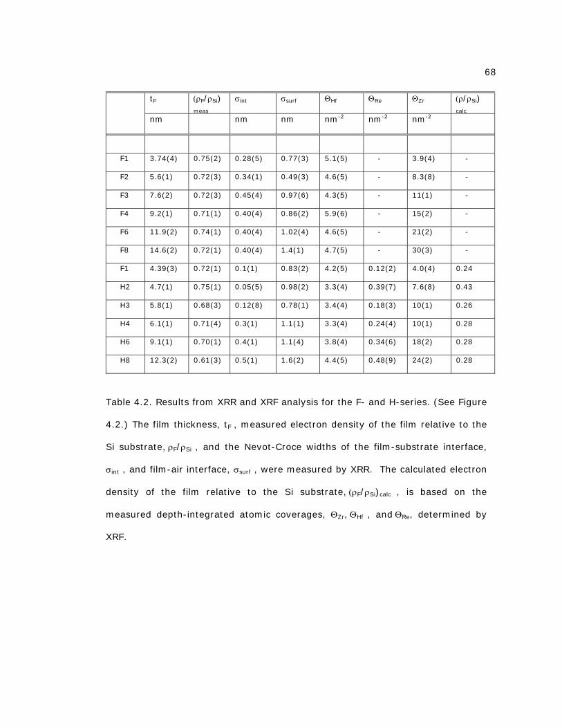
68
tF (ρF/ρSi) meas
σint σsurf ΘHf ΘRe ΘZr (ρ/ρSi) calc
nm nm nm nm-2 nm-2 nm-2
F1 3.74(4) 0.75(2) 0.28(5) 0.77(3) 5.1(5) - 3.9(4) -
F2 5.6(1) 0.72(3) 0.34(1) 0.49(3) 4.6(5) - 8.3(8) -
F3 7.6(2) 0.72(3) 0.45(4) 0.97(6) 4.3(5) - 11(1) -
F4 9.2(1) 0.71(1) 0.40(4) 0.86(2) 5.9(6) - 15(2) -
F6 11.9(2) 0.74(1) 0.40(4) 1.02(4) 4.6(5) - 21(2) -
F8 14.6(2) 0.72(1) 0.40(4) 1.4(1) 4.7(5) - 30(3) -
F1 4.39(3) 0.72(1) 0.1(1) 0.83(2) 4.2(5) 0.12(2) 4.0(4) 0.24
H2 4.7(1) 0.75(1) 0.05(5) 0.98(2) 3.3(4) 0.39(7) 7.6(8) 0.43
H3 5.8(1) 0.68(3) 0.12(8) 0.78(1) 3.4(4) 0.18(3) 10(1) 0.26
H4 6.1(1) 0.71(4) 0.3(1) 1.1(1) 3.3(4) 0.24(4) 10(1) 0.28
H6 9.1(1) 0.70(1) 0.4(1) 1.1(4) 3.8(4) 0.34(6) 18(2) 0.28
H8 12.3(2) 0.61(3) 0.5(1) 1.6(2) 4.4(5) 0.48(9) 24(2) 0.28
Table 4.2. Results from XRR and XRF analysis for the F- and H-series. (See Figure
4.2.) The film thickness, tF , measured electron density of the film relative to the
Si substrate, ρF/ρSi , and the Nevot-Croce widths of the film-substrate interface,
σint , and film-air interface, σsurf , were measured by XRR. The calculated electron
density of the film relative to the Si substrate, (ρF/ρSi)calc , is based on the
measured depth-integrated atomic coverages, ΘZr, ΘHf , and ΘRe, determined by
XRF.

69
mostly insensitive to the film thickness except at lower angles for the thickest films.
The free fitting parameters for the reflectivity model were the Si/Mo bilayer period
and the ratio of the Si to Mo layer thicknesses. Due to the variations in deposition
conditions within the sputter deposition chamber the d-spacing of the LSM was found
to vary from substrate to substrate. In addition, clamps used to hold the Si
substrates caused a shadowing near the clamps resulting in a lateral gradient of the
d-spacing. This latter problem was not significant for XSW analysis in this Chapter
Z0,Hf = 1.20 N + 1.36
Z0,Hf = 1.69 N + 1.58
tF = 1.15 N + 2.55
tF = 1.53 N + 2.63F-series
G-series
I-series
H-series (a)
(b)
Z0,Hf = 1.20 N + 1.36
Z0,Hf = 1.69 N + 1.58
tF = 1.15 N + 2.55
tF = 1.53 N + 2.63F-series
G-series
I-series
H-series (a)
(b)
Figure 4.13: XRR results for F- and H-series films. Film thickness (closed circles),
tF, and χ2 fits (solid lines). Also shown for comparison are the χ2 fits (dashed
line) of the Hf mean position z0 from the companion G- and I-series films.

70
since a small beam confined to the center of the sample was used. Thus, each
sample required a fit to the reflectivity data. A typical fit to the reflectivity is shown
in Figure 4.14a for sample film I2. The corresponding layered model is shown in
Figure 4.14b for the first two periods of the LSM. A typical X-ray fluorescence
emission spectrum of an I-series sample is shown in Figure 4.15 for sample I8. The
displayed spectrum is the angle integrated spectrum (summation of 601 individual X-
ray spectra) from the XSW scan. With the exception of the Fe Kα and Fe Kβ, all
labeled X-ray lines could be integrated to provide a characteristic XSW signature
originating from the substrate. Since the main points of interest here are the
structural properties of the metal-phosphonate films, the yield data for those metals
found in the films, namely, Hf, Zn, Re, and Zr were analyzed. The X-ray spectra for
samples in the G-series are similar to those for the I-series after the Zn and Re lines
are removed.
The G-series samples are multilayer metal-phosphonate films using Zr for the
metal layers and 1,12-dodecanediylbis(phosphonic acid) for the phosphonate layers
as shown in Figure 4.4. For each film, Hf was substituted for Zr in the final metal
layer to provide a distinct marker for the phosphonate sites at the top of the film.
The measured and calculated Hf and Zr fluorescence yields are shown for each XSW
scan in the G-series in Figures 4.16 to 4.21. The models for the χ2 fits used a
Gaussian profile ρG(z) for the Hf and a rectangular profile ρR(z) for the Zr. The free
fitting parameters for the Hf distribution were the mean position z0 and width σ of
the Gaussian distribution. The free fitting parameters for the Zr distribution were the
mid-height z0 and width ∆z of the rectangular distribution. Also included in each

71
model was an extended uniform distribution, ρE(z) to account for atoms not
contained in the assumed profiles. The final distribution was ρ(z) = C ρM(z) + (1-C)
ρE(z), where C is the partition fraction and ρM(z) is either the Gaussian or rectangular
profile. A fixed value of C = 0.85 was used for all of the distributions in the G- and
(b)
(a)
Mo Mo
SiSi Sifilm
SiO2
N = 20tBL = 18.6 nmtSi = 16.0 nmtMo = 2.6 nmtF = 5.2 nm
tSiO2 = 2.0 nmσSi/Mo = .24 nmσMo/Si = .48 nm
dXSW =4.5 nm
5.9 nm8.3 nm13.4 nm
20.9nm
(b)
(a)
Mo Mo
SiSi Sifilm
SiO2
N = 20tBL = 18.6 nmtSi = 16.0 nmtMo = 2.6 nmtF = 5.2 nm
tSiO2 = 2.0 nmσSi/Mo = .24 nmσMo/Si = .48 nm
dXSW =4.5 nm
5.9 nm8.3 nm13.4 nm
20.9nm
Figure 4.14: XRR of I2 film from XSW scan. (a)Typical measured (filled circles)
and calculated (solid line) XRR results taken simultaneously during the XSW of
sample film I2. (b) the electron density profile used to model the LSM + film
shown by plotting the real part of the index of refraction, δ. Only the first 2 of 20
LSM Si/Mo bilayers are shown. The period of the XSW is shown above each Bragg
reflection.

72
I-series. The effect of assuming an extended uniform distribution is to allow for a
component of fluorescence yield that is proportional to 1+R. The Hf and Zr
fluorescence yields of the G-series are shown as a layer sequence in Figures 4.22
and 4.23, respectively. In Figure 4.22 the changing characteristic yield profile of the
Hf can be followed as it occupies a higher and higher position with respect to the
LSM.
Si K
α
18.5 keVTDS
Mo
LαA
r Kα
Fe K
α
Fe K
β
Zr K
α
Zr L
α/P
Kα
Hf L
α
Zn K
α/R
e Lα
Hf L
β1Zn
Kβ
Re
Lβ1
Hf L
β2
Hf L
γ
Hf L
1
Zr K
β
Re
LγB
r Kα
Br K
β
Si K
α
18.5 keVTDS
Mo
LαA
r Kα
Fe K
α
Fe K
β
Zr K
α
Zr L
α/P
Kα
Hf L
α
Zn K
α/R
e Lα
Hf L
β1Zn
Kβ
Re
Lβ1
Hf L
β2
Hf L
γ
Hf L
1
Zr K
β
Re
LγB
r Kα
Br K
βFigure 4.15: Typical MCA spectrum for I-series films. Typical I-series x-ray
fluorescence spectrum showing the angle-integrated spectrum from the XSW
scan of sample I8. All labeled lines (except Fe and Br lines) give characteristic
XSW fluorescence yield curves. The G-series samples give similar spectra with
the Zn and Re lines absent.

73
Hf Zr Zn, Re
z0 σ Θ z0 ∆z Θ z0 ∆z Θ
Film nm nm nm-2 nm nm nm-2 nm nm nm-2
G1 2.76(3) 1.05(4) 5.7(6) 2.20(2) 1.50(1) 4.3(4) - - -
G2 5.81(3) 1.42(2) 7.7 (12) 3.66(3) 4.16(5) 14(2) - - -
G3 6.63(2) 1.07(2) 6.1(6) 3.80(4) 5.3(1) 13(1) - - -
G4 8.30(4) 1.30(4) 4.9(5) 4.78(5) 6.9(1) 19(2) - - -
G6 11.1(1) 1.27(4) 5.1(5) 6.41(9) 9.2(1) 23(2 - - -
G8 15.2(1) 2.30(4) 5.3(5) 8.68(2) 14.1(1) 33(3) - - -
I1 2.72(2) 0.88(3) 2.3(2) 1.72(3) 1.5 2.9(3) 2.04(3) 1.5 0.37(3)
I2 3.68(2) 1.16(2) 2.1(2) 2.08(2) 2.4 4.9(5) 2.66(2) 2.4 0.43(4)
I3 4.70(3) 1.04(3) 2.5(3) 2.65(1) 3.4 7.8(8) 3.08(2) 3.4 0.66(5)
I4 6.23(2) 1.25(2) 2.5(3) 3.25(3) 4.9 10(1) 3.94(4) 4.9 0.93(6)
I6 8.79(2) 1.42(2) 3.1(3) 4.69(3) 7.5 16(1) 5.23(4) 7.5 1.48(9)
I8 10.9(1) 1.88(4) 2.8(3) 5.47(6) 9.3 20(2) 6.49(4) 9.3 1.62(9)
Table 4.3. Results from XSW and XRF analysis for the G- and I-series samples.
(See Figure 4.4.) The mean position, z0, and width, σ, were determined from
Gaussian model profiles for the Hf atomic distribution. The mid-height, z0, and
width, ∆z, were determined from rectangular model profiles for the Zr and Zn+Re
atomic distributions. . The depth-integrated atomic coverage, ΘT, were
determined by XRF.

74
σ = 1.1 nm
σ = 0.3 nmG1
b = 1.5 nm
(a)
(c)
(b)
σ = 1.1 nm
σ = 0.3 nmG1
b = 1.5 nm
(a)
(c)
(b)
Figure 4.16: XSW results for film G1. Measured (open circles) and
calculated (solid lines) for (a) Hf yield, (b) Zr yield and (c) XRR. In (a) the
calculated result for a narrower distribution (σ=0.3 nm) is shown for
comparison. All data were collected simultaneously during a single XSW
scan

75
G2(a)
(c)
(b)
G2(a)
(c)
(b)
Figure 4.17: XSW results for film G2. Measured (open circles) and calculated
(solid lines) for (a) Hf yield, (b) Zr yield and (c) XRR. All data were collected
simultaneously during a single XSW scan

76
G3(a)
(c)
(b)
G3(a)
(c)
(b)
Figure 4.18: XSW results for film G3. Measured (open circles) and calculated
(solid lines) for (a) Hf yield, (b) Zr yield and (c) XRR. All data were collected
simultaneously during a single XSW scan

77
Figure 4.19: XSW results for film G4. Measured (open circles) and calculated (solid
lines) for (a) Hf yield, (b) Zr yield and (c) XRR. All data were collected simultaneously
during a single XSW scan
G4(a)
(c)
(b)
G4(a)
(c)
(b)

78
Figure 4.20: XSW results for film G6. Measured (open circles) and calculated
(solid lines) for (a) Hf yield, (b) Zr yield and (c) XRR. All data were collected
simultaneously during a single XSW scan
G6(a)
(c)
(b)
G6(a)
(c)
(b)

79
G8(a)
(c)
(b)
G8(a)
(c)
(b)
Figure 4.21: XSW results for film G8. Measured (open circles) and calculated
(solid lines) for (a) Hf yield, (b) Zr yield and (c) XRR. All data were collected
simultaneously during a single XSW scan

80
Fig
cal
dis
ato
G1
G6
G3
G2
G4
G8
z (nm)
z (nm)
z (nm)
z (nm)
z (nm)
z (nm)
G1
G6
G3
G2
G4
G8
z (nm)
z (nm)
z (nm)
z (nm)
z (nm)
z (nm)
ure 4.22: G-series XSW Hf results. Measured (open circles) and
culated(solid lines) Hf fluorescence yield of the G-series films. The atomic
tributions are scaled vertically for clarity and are not proportional to the
mic coverages

81
Fig
cal
dis
ato
G1
G6
G3
G2
G4
G8
z (nm)
z (nm)
z (nm)
z (nm)
z (nm)
z (nm)
G1
G6
G3
G2
G4
G8
z (nm)
z (nm)
z (nm)
z (nm)
z (nm)
z (nm)
ure 4.23: G-series XSW Zr results. Measured (open circles) and
culated(solid lines) Zr fluorescence yield of the G-series films. The atomic
tributions are scaled vertically for clarity and are not proportional to the
mic coverages

82
The I-series samples are very similar to the G-series except that a porphyrin
square bis(phosphonic acid) is used instead of 1,12-dodecanediylbis(phosphonic
acid) for the phosphonate layers as shown in Figure 4.4. Consequently, the same
structure is expected, but with the addition of Zn and Re which are expected to be
located at the mid-plane of the ideally configured porphyrin square molecule or
equidistant from adjacent Zr or Hf metal atom layers. The strong fluorescence lines
from Zn and Re are the Zn Kα and Re Lα x-ray lines which are only 20 eV apart and
thus were analyzed together as a single fluorescence. Although it is also possible to
see Zn Kβ and Re Lβ in the x-ray spectra, these peaks were too weak to be analyzed
over the full angle range. The measured and calculated Hf, Zn/Re and Zr yield are
shown for each XSW scan in the I-series in Figures 4.24 to 4.29. The χ2 fits were
obtained using an identical procedure as for Hf in the G-series using a Gaussian
distribution for Hf and rectangular distributions for Zn+Re and Zr. However, for the
rectangular distributions for Zn/Re and Zr, a coupling between the mid-height z0 and
width ∆z was observed in several of the I-series samples that was not observed in
the G- series. Better results were obtained by fixing the width ∆z of the profile using
a constraint based on the Hf fit result. For each sample in the series, the width ∆z of
the rectangular distribution for both the Zr and Zn/Re was set to ∆z = z0,Hf – 1.3 nm.
This value was chosen from an average of values observed when ∆z was left to be a
free fitting parameter from those samples in the I-series that did not show the
coupling between parameters. All of the model parameters for the atomic
distributions of Hf, Zn+Re and Zr are summarized in Table 4.3. The Hf, Zn/Re and Zr
yield results are plotted as a vertical sequence in Figures 4.30, 4.31, and 4.32,
respectively. In Figure 4.33 plots are given for the Hf mean position of the Gaussian

83
F
l
c
igure 4.24 XSW results for film I1: Measured (open circles) and calculated (solid
ines) for (a) Hf yield, (b) Zr yield and (c) Zr yield and XRR. All data were
ollected simultaneously during a single XSW scan
I1 (a)
(c)
(b)
I1 (a)
(c)
(b)

84
F
l
c
I2 (a)
(c)
(b)
I2 (a)
(c)
(b)
igure 4.25 XSW results for film I2: Measured (open circles) and calculated (solid
ines) for (a) Hf yield, (b) Zr yield and (c) Zr yield and XRR. All data were
ollected simultaneously during a single XSW scan

85
F
l
c
I3 (a)
(c)
(b)
I3 (a)
(c)
(b)
igure 4.26 XSW results for film I3 Measured (open circles) and calculated (solid
ines) for (a) Hf yield, (b) Zr yield and (c) Zr yield and XRR. All data were
ollected simultaneously during a single XSW scan

86
F
l
c
I4 (a)
(c)
(b)
I4 (a)
(c)
(b)
igure 4.27 XSW results for film I4 Measured (open circles) and calculated (solid
ines) for (a) Hf yield, (b) Zr yield and (c) Zr yield and XRR. All data were
ollected simultaneously during a single XSW scan

87
F
l
c
I6 (a)
(c)
(b)
I6 (a)
(c)
(b)
igure 4.28 XSW results for film I6 Measured (open circles) and calculated (solid
ines) for (a) Hf yield, (b) Zr yield and (c) Zr yield and XRR. All data were
ollected simultaneously during a single XSW scan

88
F
l
c
I8 (a)
(c)
(b)
I8 (a)
(c)
(b)
igure 4.29 XSW results for film I8 Measured (open circles) and calculated (solid
ines) for (a) Hf yield, (b) Zr yield and (c) Zr yield and XRR. All data were
ollected simultaneously during a single XSW scan

89
I1
I6
I3
I2
I4
I8
z (nm)
z (nm)
z (nm)
z (nm)
z (nm)
z (nm)
I1
I6
I3
I2
I4
I8
z (nm)
z (nm)
z (nm)
z (nm)
z (nm)
z (nm)
Figure 4.30: I-series XSW Hf results. Measured (open circles) and calculated
(solid lines) Hf fluorescence yield of the I-series films. The atomic distributions
are scaled vertically for clarity and are not proportional to the atomic coverages

90
Fig
(so
dis
cov
z (nm)
z (nm)
z (nm)
z (nm)
z (nm)
z (nm)
I1
I6
I3
I2
I4
I8
z (nm)
z (nm)
z (nm)
z (nm)
z (nm)
z (nm)
I1
I6
I3
I2
I4
I8
ure 4.31: I-series XSW Zn/Re results. Measured (open circles) and calculated
lid lines) Zn/Re fluorescence yield of the I-series films. The atomic
tributions are scaled vertically for clarity and are not proportional to the atomic
erages

91
z (nm)
z (nm)
z (nm)
z (nm)
z (nm)
z (nm)
I1
I6
I3
I2
I4
I8
z (nm)
z (nm)
z (nm)
z (nm)
z (nm)
z (nm)
I1
I6
I3
I2
I4
I8
Figure 4.32: I-series XSW Zr results. Measured (open circles) and calculated
(solid lines) Zr fluorescence yield of the I-series films. The atomic distributions
are scaled vertically for clarity and are not proportional to the atomic coverages

92
z0,Hf = 1.69 N + 1.58
z0,Hf = 1.20 N + 1.36
(a) G - series
(b) I - series
zbot,Zr
ztop, ZnRe
z0,ZnRe
z0,Zr
z0,Zr
zbottom, Zr
ztop, Zr
zbot,ZnRe
ztop, Zr
z0,Hf = 1.69 N + 1.58
z0,Hf = 1.20 N + 1.36
(a) G - series
(b) I - series
zbot,Zr
ztop, ZnRe
z0,ZnRe
z0,Zr
z0,Zr
zbottom, Zr
ztop, Zr
zbot,ZnRe
ztop, Zr
Figure 4.33: Modeled atomic heights for G- and I-series. The rectangular profiles
for Zr and Zn/Re are shown by plotting the mid-height (filled diamonds for Zr,
filled squares for ZnRe), top and bottom (open diamonds for Zr and open squares
for ZnRe). The mean position z0, of the gaussian profiles for the Hf (closed
circles).

93
Figure 4.34: Atomic coverage of the F-I series films: XRF measured atomic
coverages for Hf (filled circles), Zr (filled diamonds) and Zn or Re (filled squares)
and χ2 fits (solid lines).
F-seriesΘHf = -0.01 N + 4.9ΘZr = 3.7 N + 0.42
G-seriesΘHf = -0.10 N + 5.9ΘZr = 3.9 N + 1.2
H-seriesΘHf = 0.06 N + 2.8ΘZr = 2.9 N + 1.0
ΘZn = ΘRe = 0.10 N + 0.06
I-seriesΘHf = 0.10 N + 2.1ΘZr = 2.4 N + 0.53
ΘRe = 0.052 N + 0.041
using Re Lβ1 using ReLα / ZnKα
H-series I-series
F-seriesΘHf = -0.01 N + 4.9ΘZr = 3.7 N + 0.42
G-seriesΘHf = -0.10 N + 5.9ΘZr = 3.9 N + 1.2
H-seriesΘHf = 0.06 N + 2.8ΘZr = 2.9 N + 1.0
ΘZn = ΘRe = 0.10 N + 0.06
I-seriesΘHf = 0.10 N + 2.1ΘZr = 2.4 N + 0.53
ΘRe = 0.052 N + 0.041
using Re Lβ1 using ReLα / ZnKα
H-series I-series

94
profile and the bottom, mid-height and top of the rectangular profiles for Zr and
Zn+Re where the top and bottom are calculated from the mid-height and width. For
the G- and I-series XSW scans an As-implanted standard was used to calibrate the
coverages based on off-Bragg fluorescence emission at q = 0.162 A-1. The coverage
results for the G and I series samples are also given in Table 4.3.
4.3.5 Discussion for the F-, G-, H-, and I-series
The 1,12-dodecanediylbis(phosphonic acid) layer series (F- and G-series)
were chosen to provide a comparison of XSW analysis with previous published
structure data. The XSW determined structural properties of the G-series are given in
Figure 4.33a, where the Hf mean position, z0,Hf together with the position of the top
(ztop = z0 + ∆z/2), middle (z0) and bottom (zbot = z0 - ∆z/2) of the rectangular
profiles used to model the Zr are plotted. Also shown are χ2 fits of each parameter.
The χ2 fit of the Hf mean position gives z0, Hf = 1.69 N + 1.58 (nm). The per-layer
increase in thickness of 1.69 nm is in good agreement with previously published
values for this same system [37]. The offset value of 1.58 represents the expected
Hf mean position if it were used in place of Zr at the primer step. This value is higher
than expected based on the length of a single APTMS/phosphonate/Zr moiety that
was deposited as the primer layer and may be due to polymerization of the APTMS.
The larger than expected offset is present in all of the samples in the F-, G-, H-, and
I-series which were prepared together. For each sample in the G-series, the top of
the Zr atomic distribution is found to be very close to the Hf mean position. The
deviations of the Hf mean position from the linear trend are closely followed by the
top of the Zr rectangular profile. This is compelling evidence that these deviations

95
represent true variation in sample structure. The average value of the bottom of the
Zr atomic profiles is 1.49 nm which is close to the offset value of 1.58 nm of the Hf
mean position.
While the overall trends indicated by the Hf mean position and Zr rectangular
profile parameters are in excellent agreement with the expected layer structure,
individual samples in the series exhibit significant variation from the trends. For
example, consider the simplest case of the one layer sample, G1. From Table 4.3
note that the mean position of the Hf layer is z0 = 2.8 nm compared to z0 = 2.1 nm
for the middle of the Zr distribution giving a separation between the Hf and Zr layers
of 0.7 nm which is less than half of the per-layer thickness of 1.69 nm. The largest
deviation from the trend is sample G2 whose Hf mean position is 5.81 nm. From this
value a per-layer thickness of (5.81-1.58)/2=2.12 nm can be calculated which
suggests that the 1,12-dodecanediylbis(phosphonic acid) molecules are nearly
perpendicular to the surface. This in turn implies a higher packing density in sample
G2 which is supported by the higher than average Zr and Hf atomic coverage for this
sample (see Table 4.3 and Figure 4.34). The general observation is that while the
overall trends suggested by both the Hf and Zr atomic profiles are in excellent
agreement with the expected structure, there is significant variation of structure in
individual samples.
The I-series is based on the porphyrin square molecule whose PO3-to-PO3
axial length allows a maximum metal-to-metal layer spacing of 2.5 nm as compared
to 2.1 nm for the 1,12-dodecanediylbis(phosphonic acid) in the G-series. In Figure
4.33b the Hf mean position along with the top, middle and bottom of the rectangular
profiles for both the Zr and Zn+Re atoms are plotted. The χ2 fit of the Hf mean

96
position gives z0,Hf = 1.20 N + 1.36 (nm). The 1.20 nm per-layer value is
considerably lower than the maximum value of 2.5 nm permitted by the porphyrin
square in a perpendicular conformation. This is also lower than the XRR measured
per-layer thickness of 1.61 nm from the identical sample D8. The deviation of the Hf
mean position for any given sample in the I-series is considerably less than in the G-
series indicating that this seems to be a preferred conformation for the porphyrin
square. In Figure 4.33b the mid-height of the Zr and Zn+Re is given by the filled
diamonds and filled squares, respectively. The Zn+Re mid-height is vertically offset
from the Zr mid-height by an average value of 0.59 nm which is half of the per layer
spacing of 1.2 nm. The analysis shows that XSW analysis can measure the offset
between the rectangular distributions of Zr and Zn+Re in each sample in the series.
This is a powerful confirmation that the ordering of Zr, Zn+Re and Hf in the I-series
is precisely as we expect and is an excellent demonstration of the XSW method.
In Figure 4.34 the measured atomic coverage for the all of the samples in this
study is plotted. The Hf coverage is essentially constant in any given series and is
very close to the Zr coverage in the one layer samples. The average value of the Hf
coverage in the G- and I-series is 4.9 and 5.4 nm-2, respectively while in the F- and
H-series it is 3.7 and 2.6 nm-2, respectively. The greater capacity of the DDBPA
based films compared to PSBPA films is expected since the larger molecular footprint
of the PSBPA will have a much lower PO3 surface density than the DDBPA. Since
there are both Zn and Re atoms on the PSBPA molecules, the Zn or Re coverage
provides a measure of the coverage of the PSBPA. In Figure 4.34 the slope of the χ2
fit of the measured coverage shows that the per-layer coverage of PSBPA is 0.1 nm-
2/layer which in turn gives an average area per porphyrin square molecule of 40 nm2

97
(given 4 Zn or Re per square). Each molecule would thus occupy a 6.3 x 6.3 nm
area. From the measured per layer thickness of 1.2 nm a tilt angle of 60o from
vertical can be calculated assuming a 2.5 nm for the Zr-to-Zr distance based on
Figure 4.2. The projected width of the tilted porphyrin square molecule would then
be a 2.4 + 2.5sin(60o) = 4.6 nm assuming 2.4 nm is the distance between opposing
zinc centers (i.e. neglecting any inward or outward bowing of the
pyridyl(ethynyl)porphyrins and neglecting the van der Waals thicknesses of the
porphyrin planes) (see Figure 4.2). Thus the measured coverage agrees reasonably
well with the footprint implied by the measured per-layer thickness. Table 4.3 shows
that the Zr or Hf coverage is nearly 30 times greater than the Zn or Re coverage
implying that there must be alternate modes of incorporation in these films. One
possible mode is an extended 2-d sheet of ZrO2 or HfO2 where a fraction of the O
atoms are from the phosphonate groups and the remainder comes from the water in
the solution used for the deposition of the Hf or Zr. Since there is no heavy atom in
the DDBPA molecule, we were not able to measure the coverage of this molecule
with our present methods.
The results of the XRR analysis of the F- and H-series samples are given in
Table 4.2. Figure 4.13 shows plots of the XRR measured and χ2 fit film thickness
along with the χ2 fit of the Hf mean position for the XSW series. The XRR determined
film thickness is larger than the Hf mean position. This is to be expected since the Hf
mean position does not measure the maximum in the electron density gradient as
does the XRR method. The location of the maximum of the electron density gradient
can be estimated from the Hf atomic profile to be at z0+σ which falls close to the
XRR measured film height. The per-layer increase in film thickness indicated by the

98
slopes of the Hf mean position and XRR determined film heights are in general
agreement but it is important to note that the measurements come from separate
sample series using different initial surfaces, i.e., sputter deposited Si for the XSW
substrates versus single crystal Si for the XRR series. The XRR determined surface
roughness in Table 4.2 follows the same trend as the width of the Gaussian profiles
for the Hf, whereas the interface roughness is consistently in the 0.2-0.5 nm range
for the initial substrate roughness. For both the XRR and XSW series, the very rapid
roughening of the surface implies a large variability in tilt conformation of the
phosphonate components.
The final information from the XRR analysis is the overall electron density of
films which is given in Table 4.2. The average electron density is 0.73ρSi and 0.69ρSi
for the DDnR and PSnR series, respectively. The slightly lower electron density for
the PSnR series is consistent with the more porous structure expected for these
sample but far higher than expected based on the measured atomic coverage of Zr,
Hf and Zn+Re in the PSnX series. In Table 3.2 the electron density is calculated
according to (ρ /ρSi)calc = (ΘHf x 72 + ΘZr x 40 + ΘPS x 2284)/699/tF (72, 40 and 2284
are the number of electrons in the Hf, Zr and porphyrin square components,
respectively and 699 is the electron density of Si). The value of the electron density
based on the measured atomic coverage is only one third of that measured by XRR.
This is consistent with the previous finding[59] that there must be additional
material such as solvent molecules present in these films. A similar conclusion about
an excess electron density in the case of the DDBPA series cannot be made since
there are no heavy atom markers with which to measure the coverage.

99
4.3.6 Primer Layer Characterization
An important question regarding metal-phosphonate films is whether the
metal atom density in each metal layer depends on the PO3 density. To answer this
question the Zr coverage on the PO3 primed surface can be compared to the Hf
coverage which involves PO3 groups from the phosphonate molecules only. The
primer layer preparative steps are shown schematically in Figure 4.35. All samples in
this study were prepared using this substrate priming procedure. Due to a weak P X-
ray fluorescence signal, our XRF was not able to directly measure the coverage of P
in the primer layer. Samples A1, A2, F1, G1, H1, and I1 from this chapter (See
Figure 4.4.), as well as sample B1a from Chapter 5 contained Zr only in the primer
layer. From these samples, the surface density of PO3 functional groups can be
estimated by measuring the Zr atom coverage and assuming one Zr for each PO3
group. XRF measured coverages for these seven samples were in the range of 1.0 to
4.3 Zr atoms/nm2. It is well known that the fully hydroxylated SiO2 surface has 5 OH
groups per nm2 [60]. Each APTMS molecule can potentially occupy one to three OH
sites to imply a coverage range of APTMS/PO3/Zr moieties from 1.7 - 5 Zr/nm2 if all
OH groups are bound to APTMS molecules. The observed Zr coverage result suggests
that the primer APTMS/PO3 coverage varies somewhat but falls within the limits
suggested above. In Figure 4.35b we show the XSW results for the position of the Zr
atoms from all of the samples where the Zr is present in only a primer layer.
Samples B1a, (A1 & A8) and (G1 & I1) were prepared on separate occasions but
using essentially identical procedures in air-free glassware. Apparently, subtle
differences in preparative details are likely responsible for the variation in the
coverage and thus position of the Zr atoms in the primer layer.

100
Fi
a
χ2
0
1
2
3
4
5
0 0.5 1 1.5 2 2.5
z0,Zr (nm)
ΘZr
(nm
-2)
Si N P
O O
OSi
O
SiO
O
O H
O H
N P
O O
OZr
+
+
Step 1Hydroxylation
z0,ZrtSiO2
SiO
Si NO
Step 23-APTMS
Step 3Phosphorylation
Step 4Zirconation
(a)
(b)
B1a
A1
A8
G1
I1
0
1
2
3
4
5
0 0.5 1 1.5 2 2.5
z0,Zr (nm)
ΘZr
(nm
-2)
Si N P
O O
OSi
O
SiO
O
O H
O H
N P
O O
OZr
+
+
Step 1Hydroxylation
z0,ZrtSiO2
SiO
Si NO
Step 23-APTMS
Step 3Phosphorylation
Step 4Zirconation
(a)
(b)
B1a
A1
A8
G1
I1
gure 4.35: Primer Layer Structure. The preparative steps in the primer layer
re shown in (a) with the details given in the text. In (b) the XSW measured and
fit (solid line)of Zr mean position z0 is shown.

101
4.3.7 Metal Phosphonate Coordination Chemistry
The exact bonding structure between the PO3 groups and the metal atoms is
not known. Consider the assumption of one Zr/PO3 group as the chemical
stoichiometric ratio. (See Tables 4.1 to 4.3 for a list of XRF measured heavy atom
coverages.) For sample D8 with N = 8 layers, the Re (or Zn) measured atomic
coverage can be converted to a pe-layer coverage of 0.33 Re /nm2, which
corresponds to a macromolecular footprint of 12 nm2. (Here 4 Re (or 4 Zn) per
macromolecular square is assumed as shown in Figure 4.2) This footprint would
correspond to a 3.5 x 3.5 nm2 square, which is a reasonable random packing
density, given an approximate length of 3.2 nm for the OC-Re-porph-Re-CO shown
in Figure 4.2. The complexation, at the end-groups of the diphosphonic acid
porphyrin molecule in Figures 4.2 and 4.3(right-hand-side), is shown schematically
as one metal ion per PO3/PO3 junction. This is based solely on charge balance (at
least for zirconium(IV) and hafnium(IV)). If metal ions retain charged halo, oxo, or
hydroxo ligands, however, the metal:phosphonate ratio would likely be higher. In
layered Zr/phosphonate compounds featuring sterically undemanding alkane
spacers, continuous 2-D Zr/phosphonate layers, rather than discrete junctions, are
formed.[61] In these layers, each oxygen atom of a given phosphonate binds to a
different zirconium ion, i.e. the chelation motif simplistically sketched in Figure 4.4 is
absent. If chelation is likewise unused here, and if Zr ions retain an oxo ligand, an
alternative stoichiometry, more closely structurally resembling the known 2-D layers,
would be two zirconium ions per PO3/PO3 junction.
Based solely on this expected complexation (two metal ions per junction) and
the molecular footprint, the Zr, Hf or Y atomic coverage per layer, in for example

102
sample D8, should be 0.65 atoms/nm2. The measured Zr and Hf coverages per layer
in sample D8 are respectively 2.5 and 4.8 times higher. This excess and similar Zr,
Hf or Y excesses in the other samples, indicates that these metal ions have additional
modes of incorporation in these films.
4.3.8 Performance of the Large d-Spacing LSMs
In this thesis the use or large d-spacing LSMs is reported for the first time. It
is strongly desirable to be able to use the multiple Fourier components obtained in
the XSW scans to apply a direct methods determination of atomic distributions. In
this section the performance of the LSMs for this purpose will be considered. In the
G- and I-series films (see Figures 4.16 to 4.32, XSW scans covering 4 Bragg
reflections were presented. A 5th Bragg peak was measured but provided no
additional information and was not shown. In the earlier XSW work using samples A1
and A8, characteristic XSW modulations were observed through the 4th Bragg peak.
In the G-series and I-series, the roughness and general imperfection of the films did
no require more than the 3rd Bragg peaks. To evaluate the sensitivity of the LSM as a
probe of structure, several hypothetical atom distributions were constructed and the
yield was computed. In Figure 4.36 alternate models for the Zr distribution of sample
film I8 were considered. In particular the Zr distribution shown in Figure 4.36 was
constructed by summing the Gaussian distributions measured for Hf in samples I1,
I2, I3, I4, I6, and I8. The positions for the 5th and 7th layers were interpolated from
the I4, I6 and I8 films. The summed distributions were then shifted down by one half
of the layer thickness or 0.6 nm. The calculated yield for the distribution thus

103
Model 1Zr rectangle fromLeast squares fit
Model 2Sum of gaussian profiles based onHf least squares fits shifted by 1.2 nm5 and 7 layer gaussians interploated fron 4, 6 and 8
Model 1Zr rectangle fromLeast squares fit
Model 2Sum of gaussian profiles based onHf least squares fits shifted by 1.2 nm5 and 7 layer gaussians interploated fron 4, 6 and 8
Figure 4.36: Alternate models comparison for film I8: XSW calculated yield
comparison of film I8 for a simple rectangular distribution (dashed line) versus a
model constructed from Hf position data. The calculated yield for the two models
shows a nearly identical result.

104
F
c
(
igure 4.37: Sensitivity of model to layered vs single slab models. XSW
alculated yield comparison of film I8 for a simple rectangular distribution
dashed line) versus a model constructed from the expected layered Zr structure.

105
Fi
co
sh
gure 4.38: Sensitivity of LSM to sense layered structure. XSW calculated yield
mparison a sequence of layered films based on the I-series. The calculation is
own for the 4th and 5th Bragg peaks.

106
constructed is compared in Figure 4.36 to the simple rectangular model used earlier
shows very little difference in the two results. In Figure 4.37 a distribution was
constructed for the Zr based solely on the χ2 fit of the Zr mean position z0,Zr (see
Figure 4.33b). Once again very little difference between the rectangular and
constructed models is visible. In Figure 4.38 we show the calculated yields for a
series of Zr atomic distribution constructed as in Figure 4.37 but shown for the 4th
and 5th order Bragg reflections. There is apparently some contrast visible in the
series of yields suggesting it may be possible to resolve this level of detail using long
period LSMs.
4.4 Conclusions
In this chapter it was shown that long-period XSW is a very useful probe of
the structure of layer-by-layer assembled metal phosphonate films, providing a
simultaneous measurement from multiple atomic distribution profiles of various
shapes and sizes over length scales of 1 to 20 nm. When combined with XRF and
XRR, the ability to directly evaluate important assumptions about film chemistry and
quality is made possible. In the layer series based on 1,12-dodecanediylbis-
(phosphonic acid) the per-layer thickness was found to agree with previously
published values and metal layer atom densities of about 5 nm-2 were observed.
The Hf metal atom distributions showed that the surface roughness increases rapidly
with layer number and individual samples showed large variations from the general
trends but stayed within the constraints imposed by molecule length or maximum
layer spacing. In the porphyrin square I-series a 1.2 nm per layer spacing indicating
a 60o tilt angle of the walls of the porphyrin square away from the surface normal

107
which differed from the 1.69 nm per layer observed in sample D8. However, in both
cases, the tilt implied by the per-layer thickness agreed reasonably well with the
footprint implied by the measured atomic coverage emphasizing why it is so
important to be able to measure both the atomic distribution and coverage. The
layer density of Hf and Zr in the porphyrin square layer series was ~30 times higher
than the PO3 group density so that the primary mode of incorporation of the metals
Hf and Zr is one other than attachment to the PO3 groups and is probably a 2-d
sheet incorporating the O atoms of the PO3 groups as anchor points. The XRR
measured film thickness was found to be consistent with the XSW determined film
thickness but the XRR measured electron density indicated the presence of additional
components in the films not accounted for by the deposited metal or
organophosphate components. The large d-spacing LSM X-ray mirrors used in this
study have been shown to be excellent probes of nano-scale structure.

108
Chapter 5: Hg-poly(U) Adsorption to Charged Surfaces 5.1 Introduction
The adsorption of poly-electrolytes to charged surfaces is a classical topic in
physics that requires an understanding of the complex balance of electrostatic and
entropic forces. Interest in this topic has been driven by applications in biophysics
and colloid science but more recently advances made in nano-scale engineering have
placed more importance on these processes as nano-architectures involving DNA
molecules are developed[62-64]. Poly-electrolytes are most commonly handled and
assembled in aqueous solution in which the pH and ionic composition are used to
control the behavior of the polyelectrolyte. Strongly charged chains, including single
and double stranded DNA, are usually water soluble in monovalent salt solutions.
While condensation of counterions along the backbone of the chains reduces their
effective and electrostatic repulsion, the chains retain an overall charge and
therefore remain water-soluble. In the presence of multivalent cations of valence z ≥
3+, however, the chains condense (precipitate) into dense neutral cation-
polyelectrolyte aggregates within some range of multivalent cation
concentration[65]. The reversibility of multivalent cation-induced polyelectrolyte
condensation by controlling the ionic strength of the solution makes the process
useful for DNA delivery applications. Reversible adsorption of strong negatively
charged chains to negatively charged surfaces via multivalent cations is a powerful
technique to manipulate polynucleotides that is not well understood.

109
Experimental studies of the adsorption of polyelectrolytes are almost
exclusively done using atomic force microscopy (AFM) which can be performed in-
situ. An inherent limitation of the AFM technique is the requirement for a robust
attachment of the polyelectrolyte molecules; otherwise, the imaging fails because
mobile or loosely attached molecules create image defects. Neither can AFM provide
any information about the counterions that may be involved in the adsorption
process. The verification of many predicted regimes of DNA adsorption that involve
partial attachment, loose attachment, or ball and chain conformations are great
challenges for AFM techniques. An analytical determination of the distribution along
the surface normal for both the DNA and counterions is a highly desirable result for
the verification of theoretical predictions. For this purpose, the XSW technique
presents a good opportunity to compliment AFM studies. In this Chapter, the
conditions and physical reasons for polyelectrolyte adsorption onto like-charged
surfaces via cations are determined by following the polynucleotide adsorption
process in-situ with X-ray standing waves and by theoretically analyzing the process.
5.1.1 DNA Condensation in Bulk Solutions
It has been shown that in bulk solution polyelectrolyte molecules can be
reversibly condensed by multivalent counterions. The condensation of DNA by
spermine (3+) [65] and polystyrene sulfonate by multivalent salts [66] reveals that
the condensation only occurs when the counterion and polyelectrolyte concentrations
lie within certain bounds. An example of the bulk condensation behavior of DNA [65]
is provided in the phase diagram shown in Figure 5.1 for the DNA + spermine +
monovalent-salt system. Condensation of DNA by spermine was observed in the

110
region bet
solution w
dissolution
The obser
model and
(spermine
Figure
concentr
solutions
DNA so
Cprecip./CD
CDNA0.7
constant
5.1: Spermine concentrations Cprecip. and Credissol. versus DNA
ation. Precipitation and re-dissolution conditions were obtained for
of 150-bp fragments diluted in TE buffer and precipitation conditions for
lutions. The lines indicate three different fits: solid line, constant ratio
NA = 0.20 ± 0.02; dashed line for the precipitation, a power law Cprecip.
7 ± 0.03; dashed line for the re-dissolution of the 150-bp fragments, a
Credissol. = 105 ± 10 mM. Figure taken from reference [65].
ween the upper and lower lines. In general, the addition of spermine to a
ith DNA caused precipitation when Cspermine ≥ 0.20(2) CDNA with re-
occurring upon further addition of spermine when Cspermine ≥ 105(10) mM.
ved condensation behavior was explained by an electrostatic “ion-bridging”
is controlled by the density of adsorbed positively charged counterions
) along the negatively charged DNA backbone. The details of condensing

111
behavior depend on the charge of the polyelectrolyte and counterion and the
probability of adsorption of the counterion to a monomer of the polyelectrolyte.
Adding a monovalent salt to the system such as NaCl introduces a competition for
adsorption sites narrowing the limits within which condensation can take place. By
analogy to the observed bulk solution behavior, condensation of a polyelectrolyte to
a charged surface is expected to follow a similar behavior but where we need to
consider separately both positively and negatively charged surfaces. The adsorption
of polyelectrolytes to an oppositely charged surface has been treated
theoretically[67-69] with the prediction of a very complex phase diagram as shown
in Figure 5.2. Here multiple regimes are predicted which depend on the length scale
of charges along the polyelectrolyte, monovalent salt concentration and surface
Figure 5.2: Adsorption diagram of polyelectrolyte chains in a salt solution as a
function of surface charge density and Debye radius rD. Figure taken from
reference [69].

112
charge density. Two-dimensional as well as three-dimensional conformations with
the adsorbed polyelectrolytes extending above the surface are predicted.
5.1.2 Adsorption of Polyelectrolytes to Positively Charged Surfaces
Polyelectrolyte adsorption to oppositely charged surfaces has been
extensively studied both theoretically[67-69] and experimentally[70-73]. The
adsorption, controlled by the surface charge density and the ionic strength of the
solution, is due to the entropy gained by the release of the surface and
polyelectrolyte condensed counterions and by the strong ionic correlations formed in
the dense surface-polyelectrolyte layer. The adsorption of DNA to a positively
charged surface of dipalmitoyldimethyl ammonium propane (DPDAP) results in very
high adsorption densities [70, 72] as shown in the AFM image in Figure 5.3 where
the reported surface charge density was 4x10⁻⁵ C/cm2 = 2.5 nm-2. The effect of
monovalent salt concentration did not have significant effects on the density of
condensed DNA but did affect AFM image quality and lowered the incubation times
required to achieve fully packed DNA on the surfaces. The bright spots in the AFM
image in Figure 5.3 are imaging defects attributed to free ends of the DNA molecules
extending above the condensed layer. The concentration of DNA adsorbed to the
surface also does not depend on the free solution concentration of DNA or
monovalent salt and similar images were reported in de-ionized water. Cationic
surfaces, prepared by functionalization with amine-terminated species have also
been used to adsorb DNA[71]. However, in this case the surface density of adsorbed
DNA was much lower than on the DPDAP surface due mainly to the much lower
surface charge density.

113
5.1.3 Adsorption of Polyelectrolytes to Negatively Charged Surfaces
Figure 5.3: Adsorption of DNA to DPDAP. AFM image of closely packed Col E1
plasmid DNA molecules on DPDAP in 20 mM NaCl. The bright spots on the image
are loose ends of the DNA molecules that create scanning image defects. Figure
taken from reference [70].
Condensation of DNA to negatively charged surfaces has been studied in
great detail on the mica surface using the counterions Ni(II), Co(II), Zn(II), Ca(II),
Mg(II), La(III) and Zr(IV) (see Ref. [74] and references therein). The binding
strength of DNA is assessed by the ability to get AFM images. It was found that the
cationic radius is important in the degree and strength of adsorption by relating the

114
ability to image DNA. The counterions Ni(II), Zn(II) and Co(II) were found to be the
most effective while Ca(II) and Mg(II) were less effective. A maximum DNA
adsorption density is observed when the concentrations of Ni, Zn and Co are near 1
mM. A recent theoretical and experimental study was reported in this system using
MgCl2 [75]. In this study, the adsorption of DNA was explained by attractive forces
due to the correlation of shared counterion clouds. This mechanism required that the
mica and DNA possess similar surface charge densities which is true for DNA and
mica. Pretreatment of mica by the divalent ion, Ni2+, enhances the adsorption by
reducing the mica surface charge density. In all the above cited studies, there is no
measurement of the adsorption density of the counterions. Studies demonstrating
the adsorption of DNA to a negatively charged surface prepared by the hydroxylation
of a silica surface have not been found.
5.1.4 Strategy for In-Situ Measurement of Hg-poly(U) Adsorption
In this chapter we seek to understand the adsorption of Hg-poly(U) to an
anionic hydroxyl-terminated SiOx surface using Zn2+ counterion mediated attraction.
The choice of using Hg-poly(U) was motivated by the fact that the mercuration of
bases is 100% so that in the XSW measurements, the number of Hg atoms is
equated with the number charges on the poly(U) molecules. A schematic diagram of
the adsorption scheme is shown in Figure 5.4. The distribution of the Zn and Hg
atoms normal to the adsorbing surface will reveal the structure of the adsorbed
conformation, which by analogy with the observed self-condensation behavior of
polyelectrolytes described above, is only expected to occur within relatively narrow
limits of relative concentration of Zn and Hg-poly(U). In Figure 5.4 we show the Hg

115
ZnO-
Si++
N
HN
H
H
O
O
O
O-
O
Hg
H OH
H OH
O
O
P
…
OH
Si
OH
Si
OH
Si
O
Si
O-
Si
ZnO-
Si
++
OH
Si
OH
Si
Zn +chemicallybound Zn
electrostaticallybound Zn
OH
Si
OH
Si
O
Si
O-
Si
Zn +
N
HN
H
H
O
O
O
O-
O
Hg
H OH
H OH
O
O
P
OH
Si
Ion-BridgingChemisorption/Physisorption
20 layer pairs …MoMo
Si Mo
Mo
Si
Si
~ 1 nm
ZnO-
Si++
N
HN
H
H
O
O
O
O-
O
Hg
H OH
H OH
O
O
P
N
HN
H
H
O
O
O
O-
O
Hg
H OH
H OH
O
O
P
…
OH
Si
OH
Si
OH
Si
O
Si
O-
Si
ZnO-
Si
++
OH
Si
OH
Si
Zn +chemicallybound Zn
electrostaticallybound Zn
OH
Si
OH
Si
O
Si
O-
Si
Zn +
N
HN
H
H
O
O
O
O-
O
Hg
H OH
H OH
O
O
P
N
HN
H
H
O
O
O
O-
O
Hg
H OH
H OH
O
O
P
OH
Si
Ion-BridgingChemisorption/Physisorption
20 layer pairs …MoMo
Si Mo
Mo
Si
Si
~ 1 nm
Figure 5.4: Schematic diagram of Zn2+ mediated Hg-poly(U) adsorption to an O-
(H+) surface. Surface hydroxyl groups can be either un-dissociated (OH),
dissociated (O-) or Zn reacted (ZnO+). Two models of adsorption are shown. In (a)
the Zn is chemically bound. In (b) the Zn remains a +2 aqueous ion and the
adsorption is by an “ion-bridging” mechanism. The diagram also shows the
position of Hg attachment onto the RNA and the expected physical separation from
the adsorbed Zn ions.

116
atoms approximately one-half of a width of the RNA molecule away from the surface,
or Zn atom. This distance is less ~1.0 nm and could be less depending on the actual
atomic arrangement of the base and overall tilt of the adsorbed monomer with
respect to the substrate.
Surface hydroxyl atoms can be either un-dissociated (uncharged) or
dissociated (charged). Zn can also react (chemisorption) with the surface hydroxyl
groups, effectively inverting the charge from (-) to (+). The adsorption of Hg-poly(U)
via Zn is postulated to occur by one or both of the mechanisms indicated in Figure
5.4. An aqueous solution of Hg-poly(U) and ZnCl2 are placed in contact with the
hydroxylated SiO2 surface. The available experimental ranges of concentration of Zn
and Hg is limited by the need to maintain sensitivity of adsorbed atoms with respect
to bulk atoms. For example, given an adsorbed Zn coverage of 0.1 atoms per nm2,
the value of the bulk concentration which contains an equal amount of Zn in 5 µm of
bulk solution is 33 µM. In other words, 0.1 atoms per nm2 on the surface will project
to a bulk concentration of 33 µM in 5 µm of solution above. Greater sensitivity to the
adsorbed Zn will be achieved if the solution thickness is smaller, the surface
concentration is higher, or if the bulk concentration lower and so forth. We can see
that if the surface coverage of Zn does not exceed 0.1 nm-2, then observing
adsorption from 330 µM ZnCl2, for example, will be very difficult because only 10%
of the fluorescent Zn X-rays will originate from the adsorbed layer atoms. The Zn
coverage given in the preceding discussion is typical of adsorption onto hydroxylated
SiOx surface so for this reason, the range of Zn bulk concentration is confined to a
range of about 5-200 µM. In addition to measuring the adsorption behavior of the

117
combined Hg-poly(U) + Zn system, we also need to measure the adsorption
behavior of Zn in the absence of the poly(U) to understand how or even if Zn might
pre-adsorb to the substrate.
While the primary objective of this study was to measure the adsorption
behavior in the Zn/Hg-poly(U) system, some simpler but related experiments were
performed using the Hg-poly(U) and/or Zn alone. Hg-poly(U) was adsorbed to
positively charged surfaces formed by functionalizing with (a) amine or (b) Zr4+. Zn
was adsorbed to a negatively charge surface formed by functionalizing with a PO3
terminated surface. These alternate systems provide additional measurements with
results that compliment and strengthen the in-situ Zn/Hg-poly(U) studies.
5.1.5 Charging Behavior of the Planar SiO2 Surface
While the surface density of silanol groups is well known to be in the 5-8 nm-2
range for all forms of silica[76], the surface charge density or degree of dissociation
depends on the bulk solution chemistry and can be altered by the presence of macro
ions in the vicinity of the surface. The hydroxylated silica surface acquires a charge
by the following reaction,
+− +⎯→⎯ HSiOSiOH (5.1)
A planar surface has a very low specific area so that the concentration of H+ is
controlled by the bulk solution ionic strength and pH. The surface charge density is
described by the mass action law,
pK
SiOH
SiO0 10]H[ −
+
=−
ΓΓ
(5.2)

118
where [H+]0 is the hydronium ion concentration the surface which depends on the
surface potential, is the surface density of dissociated sites and is the
surface density of chargeable sites which varies between 5-8 nm
−SiOΓ SiOHΓ
-2 and pK = 7.5 [77].
From Ref. [76] an estimate of the effective charge for the silanol surfaces used in this
study assuming a pH = 7 and ionic strength ~ 10-4 is −SiOΓ = 0.01 nm-2. The effective
charge increases with pH and ionic strength.
5.2 Experimental Details
All substrates used in the XSW measurements of Zn and poly(U) adsorption
were Si/Mo LSM x-ray mirrors whose top surface was the oxide of the final sputter
deposited Si layer. This top surface was modified by chemical treatment to provide
various charged surfaces for Hg-poly(U) adsorption studies. LSM substrates with a d-
spacing of 21.6 nm were used for ex-situ experiments performed at the NSLS X15A.
In-situ experiments were performed at ESRF using ID32 using 18.6 nm d-spacing
substrates and the LSI cell both described in Chapter 3. All other experimental
details are described below.
5.2.1 Mercuration of Polyuridylic Acid
Polyuridylic acid poly(U) can be 100% mercurated[78]. Polyuridylic Acid(5’)
potassium salt (2380-2900 units) was obtained from Sigma Chemical Co. (St. Louis,
MO) and was dialyzed in sodium acetate solution (5 mM CH3COONa, pH 6.0 ) to
remove low molecular weight material prior to use. Dialysis was continued for 24 h
with buffer changes every 8 h. After dialysis, 0.6 mM mercuric acetate was added to

119
4mM poly(U) and kept at 50oC for 5 h. Quench buffer (10 mM Tris-HCl (pH 7.5)-0.1
M EDTA-1.0 M NaCl) is added to the solution at the end of the mercuration reaction.
The product was dialyzed at 4oC against TNE buffer (10 mM Tris-HCl (pH 7.5)- 1 mM
EDTA- 20 mM NaCl) for 48 h with buffer changes every 12 h. Finally, dialysis was
performed against DI water for 72 hours to reduce NaCl. Compared with the UV
spectra of Poly(U), the maximum absorption peak of Hg-Poly(U) has a 5 nm red
shift. The unit weight of Hg-poly(U) is 563 Da. After extensively dialysis, we assume
all the Hg atoms in solution are covalent bonded on poly(U). The preceding
preparation was taken from Dale et al [78]. These authors also provide extensive
evidence that Hg-poly(U) retains its biological function despite the Hg attachment.
Two points of concern are that (a) some catalysts can rapidly demercurate the Hg-
poly(U) and (b) Hg-poly(U) is thermolabile so that prolonged exposure at elevated
temperature leads to demercuration. For example, 24 hours at 37oC leads to about
15% demercuration.
5.2.2 Sample Preparation
In sample A1b, Hg-poly(U) was adsorbed to a 21.6 nm d-spacing LSM
substrate functionalized to an amine-terminated (NH3+) surface. The functionalization
of the LSM substrate to an amine surface was performed as follows: the surface was
cleaned in piranha solution (2:1, sulfuric acid: hydrogen peroxide) to remove organic
contaminants from the surface, rinsed with ultrapure Millipore water and dried under
a stream of N2 gas. Immediately afterwards, the substrate was placed in 2 M HCl for
5 min, rinsed with ultrapure-water, dried under a stream of N2 gas, and oven-dried
at 80 oC for 15 min. The substrate was then placed in an 80oC solution of anhydrous

120
octanol and 3-aminopropyl-trimethoxysilane (APTMS) (100:1 v:v) for 10 min, rinsed
with hexanes and ultrapure-water, dried under a stream of N2 gas, and dried in an
oven at 80oC for 30 min. Adsorption of the Hg-Poly(U) was done placing 120 µL of
165 µM Hg-poly(U) directly onto the NH3 terminated substrate surface for 10
minutes. The solution was rapidly blown off with a stream of N2 gas taking care not
to leave drops which would evaporate leaving large agglomerates particles of Hg-
poly(U). XSW measurement was performed on the sample in a N2 purged
environment.
Sample B1a was prepared by adsorbing Hg-poly(U) to a Zr-functionalized
21.6 nm d-spacing LSM surface. The substrate surface was prepared identically to
sample A1b with the following additional steps: Phosphorylation of the amine-
terminated surface was done by immersion in a mixture of 0.1 M POCl3 and 0.1 M
2,4,6-collidine in anhydrous acetonitrile (ACN) for 1 h followed by heating in warm,
dry ACN for 15 min, followed by rinses with ACN and Millipore water and then dried
under a stream of dry N2. Zirconation was done by immersion in an aqueous solution
of 5 mM ZrOCl2•8H2O for 2 h, rinsed with Millipore water, and dried under a stream
of dry N2 to yield a Zr surface. Adsorption of the Hg-Poly(U) followed by placing 200
mL of 137 µM Hg-poly(U) directly onto the Zr-funtionalized surface and let incubate
at room temperature for 10 min. The liquid was then rapidly blown off with a stream
of N2 gas.
Sample JL_C1 was prepared for in-situ observation of Zn2+ adsorption to a
PO3-functionalized 18.6 nm d-spacing LSM surface. The substrate surface was
prepared identically to sample B1a with the following additional steps: A monolayer
of 1,12-dodecanediylbis(phosphonic acid) (DDBPA) was deposited after the Zr-

121
functionalization step by immersion in 5 mM DDBPA in 60% ethanolic solution
overnight.
Samples JL817OH_A and JL817BOH_A were prepared for in-situ observation
of Zn2+ adsorption or Zn-mediated adsorption of Hg-poly(U) to negatively charged
surfaces prepared by hydroxylation of LSM substrates. Fresh LSM substrates (SiOx
top surface) were cleaned in piranha solution (2:1, sulfuric acid: hydrogen peroxide)
to remove organic contaminants from the surface and then rinsed with Millipore
water and dried under a stream of N2. Immediately afterwards, the substrate was
hydroxylated by immersion in 2M HCl for 5 min, rinsed with Millipore water and dried
under a stream of dry N2. Fully hydroxylated surfaces have a surface hydroxyl group
density of 5 nm-2 [79]. The substrates were then used in the solid-liquid interface-
cell described in Chapter 3 for in-situ studies of the adsorption of Hg-poly(U) using
various aqueous mixtures of Hg-poly(U) and ZnCl2.
5.2.3 Ex-Situ XSW Measurements
XSW measurement of samples A1b and B1a was performed in the dry state
after adsorption of the Hg-poly(U) at the NSLS X15A using Eγ= 12.4 keV (λ = 1.00
Å) incident x-rays to excite Hg L fluorescence for sample A1b and Eγ= 18.3 keV (λ =
0.674 Å) incident x-rays to excite Hg L and Zr K fluorescence for sample B1a.
5.2.4 In-situ XSW Measurements
In-situ XSW measurements using the LSI cell for samples JL817BOH_A,
JL_C1, and JL817OH_A were performed at the ESRF ID32 beamline as described in
Chapter 2. Incident X-rays with Eγ= 14.3 keV (λ = 0.867 Å) were used for sample

122
JL817BOH_A to excite Zn Kα, Hg Lα, and Hg Lβ fluorescence. Incident X-rays with
Eγ= 12.4 keV (λ = 1.0 Å) were used for samples JL_C1 and JL817OH_A to excite Zn
Kα and Hg Lα fluorescence.
5.3 Ex-Situ XSW Hg-poly(U) Adsorption Results
5.3.1 Adsorption of Hg-poly(U) to an Amine-Terminated Surface
The measurement of polynucleotide adsorption to a positively charged surface
was motivated primarily by the desire to test the XSW measurement scheme for a
simpler configuration. By doing so we verify that the Hg atoms are attached to the
poly(U) as expected. In sample A1b, we measure the adsorption of Hg-poly(U) to an
amine (NH3+) terminated surface and in sample B1a we measure the adsorption of
Hg-poly(U) to a Zr surface. XSW measurement of A1b was taken by scanning over θ
= 0.08o to 0.6o. Figure 5.5 shows angle-integrated X-ray spectra for the angle range
of θ = 0.12o to 0.36o. We see Si Kα, Mo Lα, Ar Kα, W Lα and W Lβ1 which originate
for the LSM substrate with W being an impurity in the Mo layers and Ar being an
impurity in the Si layers. Cu Kα and Zn Kα are present as environmental impurities
and Hg Lα is present from the adsorbed Hg-poly(U) and is the only signal originating
from the surface of the sample. The proximity of W Lβ1 and Hg Lα in the X-ray
spectrum requires careful fitting especially since the W exhibits strong modulations
across the Bragg peaks. This difficulty becomes worse at higher angles where the
penetration of incident X-rays into the substrate is higher and thus W fluorescence

123
becomes stronger relative to Hg. Prior to taking the XSW scans, a fast reflectivity
scan was taken and used for the modeling of the substrate reflectivity properties. In
Figure 5.6a the reflectivity from the fast scan is shown with excellent agreement
between the measured and theoretical reflectivity. In Figure 5.6b we show the
measured and theoretical Hg fluorescence yield. The functional form used to model
the Hg, ρHg(z), was: (i) A Gaussian model characterized by a mean position z0 and
spread σ, and (ii) an extended uniform distribution (rectangular profile from z = 0 to
z = tF +200 nm ) representing a disordered fraction. The Hg was thus modeled as
ρHg(z) = CHg x (i) + (1-CHg) x (ii). The best fit yielded z0 = 1.0 nm, σ = 0.5 nm and
1.E+03
1.E+04
1.E+05
1.E+06
0 2 4 6 8 10 12X-ray energy (keV)
mca
cou
nts
Si K
α
12.4 keVTDS
Mo
Lα
Ar K
α
W L
αZn
Kα
Cu
Kα
Fe K
α
Puls
er
Fe K
β
Hg
LαW
Lβ1
1.E+03
1.E+04
1.E+05
1.E+06
0 2 4 6 8 10 12X-ray energy (keV)
mca
cou
nts
Si K
α
12.4 keVTDS
Mo
Lα
Ar K
α
W L
αZn
Kα
Cu
Kα
Fe K
α
Puls
er
Fe K
β
Hg
LαW
Lβ1
Figure 5.5: MCA Spectrum for sample A1b. The angle integrated X-ray spectrum
from the XSW measurement of sample A1b taken at Eγ = 12.40 keV.

124
Figure
termina
reflectiv
(c) mea
Bragg p
the sur
Hg-poly
(a)
(b)
(c)Si C
H
HCH
HCH
HN
Si/Mo LSM
-
Hg
Hg
Hg-
-
H+H
H
Gaussian: z0 = 1.0 nm, σ = 0.3 nm, C = 0.8
z0 = 1.5 nm1.0 nm0.5 nm
(a)
(b)
(c)Si C
H
HCH
HCH
HN
Si/Mo LSM
-
Hg
Hg
Hg-
-
H+H
H
Si CH
HCH
HCH
HN
Si/Mo LSM
-
Hg
Hg
Hg-
-
H+H
H
Gaussian: z0 = 1.0 nm, σ = 0.3 nm, C = 0.8
z0 = 1.5 nm1.0 nm0.5 nm
5.6: XSW Results for sample A1b. Hg-poly(U) adsorption to an amine-
ted Si/Mo LSM; (a) measured (filled circles) and calculated (solid line)
ity, (b) measured (filled circles) and calculated (solid line) Hg yield and
sured (filled circles) and calculated (solid lines) Hg yield for the 3rd and 4th
eaks for various values of the mean position, z0. The inset in (c) shows
face functionalization by 3-aminopropyl(trimethoxy) silane and scheme for
(U) attachment.

125
CHg = 0.8 which indicates that the Hg atoms are very close to SiO2 surface. The
mean position determined to be 1.0 nm is consistent with the expected primer layer
and RNA molecule dimensions. In Figure 5.6c theoretical yield curves for several
alternate values of the mean position, z0 = 0.5, 1.0 and 1.5 nm are shown to indicate
the sensitivity to this parameter.
5.3.2 Adsorption of Hg-poly(U) to a Zr-Terminated Surface
Hg-poly(U) was adsorbed to a Zr terminated surface in Sample B1a as
described above. XSW measurement of B1a was taken at 18.20 keV in order to
excite X-ray fluorescence from both Zr and Hg atoms. The angle integrated X-ray
fluorescence spectrum is shown in Figure 5.7. The same X-ray lines appear as in
sample A1b with the addition of Zr Kα and Hg Lβ. Sample B1a was also analyzed
with XSW using 12.40 keV incident X-rays and the X-ray fluorescence spectrum was
identical to that shown in Figure 5.5 for sample A1b. The experimental XSW
fluorescence yields for both measurements are shown in Figure 5.8. Due to the low
photon flux at 18.50 keV at the X15A beamline, a large 10 mm wide X-ray beam was
required for this measurement. Unfortunately, this large beam averaged the large
lateral variation of the d-spacing of LSM substrate resulting in reflectivity data could
not be modeled well using our standard modeling techniques. For this reason the
XSW analysis gave poor fits to the reflectivity and fluorescence yield but qualitative
interpretation was still possible. Previous experience with various XSW yield profiles
indicates that the Hg and Zr are contained in narrow distributions close to the
substrate surface. The sharp kinks in Figure 5.8b indicate that the atomic distribution
is very narrow. The asymmetry towards the high side of the Bragg peaks indicates

126
that the center of the distribution is very near the surface. The similarity of the Hg
fluorescence yield profile taken at 12.4 keV in samples B1a(Figure 5.8a,b) and A1b
(Figure 5.6b) suggest that the Hg atomic yield for profiles are very similar for both
samples although the sharper kinks in the Hg sample B1a suggest that the
distribution may be narrower than in sample A1b. The fluorescence yield data taken
at 18.3 keV for sample B1a shown in Figure 5.8c indicate that the Zr and Hg atoms
appear to be in very nearly the same location because their fluorescence yield
profiles are nearly identical. Apparently, the Hg and Zr atoms are narrowly confined
to the surface of the substrate. The positions of the Hg and Zr atoms are likely to be
1.E+03
1.E+04
1.E+05
1.E+06
0 5 10 15 20X-ray energy (keV)
mca
cou
nts
Si K
α
18.3 keVTDS
Mo
LαA
r Kα
W L
αZn
Kα
Cu
Kα
Fe K
α
Puls
er
Fe K
β
Hg
LαW
Lβ1
Hg
Lβ1
Zr K
α
1.E+03
1.E+04
1.E+05
1.E+06
0 5 10 15 20X-ray energy (keV)
mca
cou
nts
Si K
α
18.3 keVTDS
Mo
LαA
r Kα
W L
αZn
Kα
Cu
Kα
Fe K
α
Puls
er
Fe K
β
Hg
LαW
Lβ1
Hg
Lβ1
Zr K
α
Figure 5.7: MCA Spectrum for sample B1a. The angle integrated X-ray spectrum
from the XSW measurement of sample B1a taken at Eγ = 18.30 keV.

127
(c)
(b)
(a)
Si CH
HCH
HCH
HN
Si/Mo LSM
-
Hg
Hg
Hg-
-
PH
H O O
OZr
+
+(c)
(b)
(a)
Si CH
HCH
HCH
HN
Si/Mo LSM
-
Hg
Hg
Hg-
-
PH
H O O
OZr
+
+Si CH
HCH
HCH
HN
Si/Mo LSM
-
Hg
Hg
Hg-
-
PH
H O O
OZr
+
+
Figure 5.8 XSW results for sample B1a. Hg-poly(U) adsorption onto a Zr-
terminated surface; (a) experimental (open circles) and calculated (solid line)
reflectivity taken at 12.40 keV, (b) measured (open circles) and calculated (solid
line) Hg yield taken at 12.40 keV and (c) measured (open circles) reflectivity, Hg
yield (filled circles) and Zr (filled squares) fluorescence yield taken at 18.50 keV.

128
within 0.5 nm of each other. An examination of the simulations at the 4th Bragg peak
in Figure 5.6c show that a 0.5 nm separation would give a noticeable difference in
fluorescent yield profiles and the similarity of the Hg and Zr profiles in Figure 5.8c
leads us to this conclusion. Coverage measurements performed on sample B1a
revealed a Zr atomic coverage of 1.6 nm-2 and an Hg atomic coverage of 0.019 nm-2.
5.4 In-Situ XSW Zn and Hg-poly(U) Adsorption Results
XSW measurement of the absorption of Hg-poly(U) to a negatively charged
surface using Zn counterion mediated attraction was performed in-situ using the
liquid-solid interface (LSI) cell described in Chapter 3. The concentrations [Zn2+] =
50 µM and [Hg-poly(U)] = 25 µM were chosen based on experimental and
theoretical considerations as discussed above. The modeling of the X-ray reflectivity
from measurements using the in-situ LSI cell is accomplished by simply adding one
water and one Kapton layer to the LSM model. The thickness of the water is
unknown while the thickness of the Kapton is 7 µm. In Figure 5.9 the measured
reflectivity for a typical in-situ sample with water and Kapton layers is shown along
with several intermediate steps of prediction to demonstrate the details of the
modeling procedure. The inset in Figure 5.9b shows the LSM model with the added
water and Kapton layers. The remainder of the layered model is just the typical LSM
model refined from ex-situ studies presented throughout this thesis. The ZnCl2 (and
Hg-poly(U)) are taken to have a negligible effect on the scattering properties of the
water layer. When very large thickness layers are present, the dynamical scattering
theory predicts high frequency oscillations. For example, for a single 12 µm layer,

129
E = 12.4 keV
tKapton = 7 µm
tW = 3.0 µm
∆q0.02 = 0.025
tKapton = 0.1 nmtW = 0.1 nm
tKapton = 7000 nmtW = 3000 nm
z
0solution layer
Kapton film
Si/Mo LSM
tKapton
tW
(a)
(b)E = 12.4 keV
tKapton = 7 µm
tW = 3.0 µm
∆q0.02 = 0.025
tKapton = 0.1 nmtW = 0.1 nm
tKapton = 7000 nmtW = 3000 nm
z
0solution layer
Kapton film
Si/Mo LSM
tKapton
tW
(a)
(b)
Figure 5.9: Modeling details of in-situ reflectivity. (a) Measured (filled circles) and
calculated (solid lines) reflectivity from the in-situ LSI cell. The heavy solid line in
(a) is the calculation without Kapton and water for comparison. The thin solid line
in (a) adds the Kapton and water and shows high frequency oscillations due to the
very large thickness of these layers. In (b) the calculated (solid line) reflectivity
after applying a footprint related angle averaging.

130
thickness fringes of period 1/d = 8e-6 Å-1 are predicted but are never observed
experimentally because of the high waviness of the Kapton surface. Smoothing is
used to eliminate the high frequency oscillations predicted by the model which
simulates the effect of the waviness of the Kapton surface. However, for the in-situ
measurements reported here, we also observe an apparent foot-print related angle-
averaging which may be due to warping of the substrate due to the force of the
Kapton film on the sample edges. This angle-averaging exceeds in general the angle-
averaging necessary to smooth the high frequency oscillations. To account for the
apparent substrate warping, a boxcar angle-averaging proportional to 1/q is
implemented as follows:
∑+=
−=+=
2/nij
2/nijjsmeared )1n/()q(R)q(R
i
where n includes a range of points spanning ∆qi which is computed at each point
according to,
( )min
i
min02.0i q
qqq02.0q ∆+
∆−∆=∆
where ∆q0.02 is a ∆qi at q = 0.02 Å-1 and ∆qmin is an asymptotic value to account for
angle-averaging due to roughness at high angle where the footprint related angle-
averaging dies off. We apply this angle-averaging to the calculated reflectivity.
Figure 5.9a shows the calculated reflectivity for the LSM alone with and without the
water and Kapton layers and without applying any angle-averaging calculation. Note
that the critical angle in this case corresponds to the effective δ of the Si/Mo LSM.
When the water and Kapton layers are added but no angle averaging applied, the
thickness oscillations can be seen. In Figure 5.9b the final theoretical reflectivity is

131
shown in which a footprint related angle-averaging has been applied using ∆q0.02 =
0.025 Å-1 (corresponding to an approximate radius of curvature of 7m) and ∆qmin =
0.001 Å-1. The fitting of the water layer thickness was done after the determination
of the smoothing parameters.
5.4.1 In-situ Adsorption of Zn2+ to an OH Surface
The adsorption of Zn2+ in the absence of poly(U) constitutes a baseline
measurement. In sample JL817BOH_A Zn2+ was exposed to an OH- terminated
SiO2/LSM surface using 50 µM ZnCl2 solution. XSW measurements were made using
14.3 keV X-rays. Figure 5.10 shows the angle integrated MCA spectrum and Figure
5.11 shows the XSW results which are also tabulated in Table 5.1.
The measured and calculated Zn fluorescence yield is shown in Figure 5.11b
which clearly shows a condensed Zn layer. The reflectivity was modeled as described
above and gave a water layer thickness, tW = 2.41 µm. The E-field intensity is
computed in the normal fashion using the LSM model determined from the
reflectivity fit shown in Figure 5.11a. The E-field intensity was computed in the water
layer at the following z positions; z = 0-20 nm with ∆z = 0.1 nm and z = 20 -3000
nm with ∆z = 10.0 nm. Prior to performing the Zn atom distribution model
calculations, the same angle averaging that was determined from the reflectivity fit
was applied to the E-field intensity. The Zn atom distribution was modeled using a
rectangular distribution, ρS(z), with one edge fixed at z=0 and the other edge
defined by z=tZn left as a free fitting parameter. The mean position, z0,Zn, of the Zn is
just the center of the rectangular distribution. The bulk Zn atoms were modeled

132
using a uniform distribution, ρB(z) over the entire water layer. The total Zn yield was
ρZn(z) = CZn ρS(z) + (1-CZn) ρB(z), where CZn is the fraction in the surface condensed
layer modeled by ρS(z). When there is no surface condensed layer then we have CZn
= 0. The attenuation of the incident beam by the Kapton and water was accounted
for by using the XSW calculated yield at the off-Bragg position which takes into
account the model distribution of the Zn. The attenuation of exiting fluorescence was
1.E+03
1.E+04
1.E+05
1.E+06
0 5 10 15 20X-ray energy (keV)
mca
cou
nts
Si K
α 14.3 keVTDSM
o Lα
Ca
Kα
W L
αZn
Kα
Cu
Kα
Fe K
α
W L
β1
Ca
Kβ
Mo
Kα
Mo
Kβ
Ar K
α
Fe K
β
W L
β21.E+03
1.E+04
1.E+05
1.E+06
0 5 10 15 20X-ray energy (keV)
mca
cou
nts
Si K
α 14.3 keVTDSM
o Lα
Ca
Kα
W L
αZn
Kα
Cu
Kα
Fe K
α
W L
β1
Ca
Kβ
Mo
Kα
Mo
Kβ
Ar K
α
Fe K
β
W L
β2
Figure 5.10: MCA Spectrum for sample JL817BOH_A. The angle integrated X-ray
spectrum from the XSW measurement of sample JL817BOH_A taken at Eγ =
14.30 keV.

133
Figure 5.11: In-situ XSW result for 50 µM ZnCl2 placed in contact with an OH
terminated LSM/SiO2 substrate. (a) Model atomic distribution (b) Measured
(filled circles) and theoretical Zn yield for various values of the coherent fraction
CZn. The line for CZn = 0.0 is equivalent to the case where all Zn in contained in
the bulk solution only and for CZn = 1.0 all Zn is condensed on the surface. (c)
Measured (closed circles) and calculated (solid line) in-situ reflectivity. The
dashed line shows the calculated reflectivity with no Kapton or water.
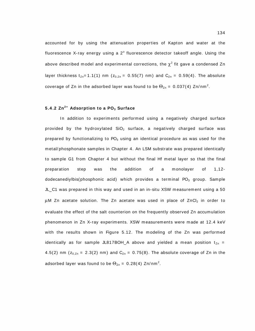
134
accounted for by using the attenuation properties of Kapton and water at the
fluorescence X-ray energy using a 2o fluorescence detector takeoff angle. Using the
above described model and experimental corrections, the χ2 fit gave a condensed Zn
layer thickness tZn=1.1(1) nm (z0,Zn = 0.55(7) nm) and CZn = 0.59(4). The absolute
coverage of Zn in the adsorbed layer was found to be ΘZn = 0.037(4) Zn/nm2.
5.4.2 Zn2+ Adsorption to a PO3 Surface
In addition to experiments performed using a negatively charged surface
provided by the hydroxylated SiO2 surface, a negatively charged surface was
prepared by functionalizing to PO3 using an identical procedure as was used for the
metal/phosphonate samples in Chapter 4. An LSM substrate was prepared identically
to sample G1 from Chapter 4 but without the final Hf metal layer so that the final
preparation step was the addition of a monolayer of 1,12-
dodecanediylbis(phosphonic acid) which provides a terminal PO3 group. Sample
JL_C1 was prepared in this way and used in an in-situ XSW measurement using a 50
µM Zn acetate solution. The Zn acetate was used in place of ZnCl2 in order to
evaluate the effect of the salt counterion on the frequently observed Zn accumulation
phenomenon in Zn X-ray experiments. XSW measurements were made at 12.4 keV
with the results shown in Figure 5.12. The modeling of the Zn was performed
identically as for sample JL817BOH_A above and yielded a mean position tZn =
4.5(2) nm (z0,Zn = 2.3(2) nm) and CZn = 0.75(8). The absolute coverage of Zn in the
adsorbed layer was found to be ΘZn = 0.28(4) Zn/nm2.

135
Figur
of Zn
subst
blue
calcu
struc
CZn = 0.75 (8)
z0,Zn = 2.3 (1)
∆z = 4.5 (2)
[Zn] = 51(5) µM
(a)
(b)
O-O
O-
O
O P
O
PZrOO
OP Zn
+
+
LSM
CZn = 0.75 (8)
z0,Zn = 2.3 (1)
∆z = 4.5 (2)
[Zn] = 51(5) µM
(a)
(b)
O-O
O-
O
O P
O
PZrOO
OP Zn
+
+
LSM O-O
O-
O
O P
O
PZrOO
OP Zn
+
+
O-O
O-
O
O P
O
PZrOO
OP Zn
+
+
LSM
e 5.12: Adsorption of Zn to a PO3 surface. In-situ XSW results for adsorption
from 50 mM Zn acetate placed in contact with an PO32- terminated LSM
rate. (a) Measured (closed circles) and calculated Zn yield for CZn=0 (solid
line) and CZn=0.75 (solid black line) (b) Measured (filled circles) and
lated (solid red line) X-ray reflectivity. The inset show the schematic
ture of the surface preparation and expected configuration for Zn adsorption.

136
5.4.3 Hg-poly(U) Adsorption to an OH Surface
The adsorption of Hg-poly(U) was examined by XSW measurement of sample
JL817OH_A using a solution with 50 µm ZnCl2 and 25 µM Hg-poly(U). The solution
was let incubate for 1 hour prior to the first XSW scan. Six scans of 30 min duration
each were taken, two each at lateral positions x = 0.0, 1.5, and 3.0 mm. The total
time between the start of the 1st scan and end of the 6th was 180 minutes The initial
plan was to measure the Zn and Hg atom distribution twice at several locations to
check for consistency both spatially and in time. Instead we observed a time
dependent phenomenon as equilibrium had not been established after a 1-hour
incubation period. An angle integrated X-ray spectrum is shown in Figure 5.13. We
see Zn Kα with an adjacent W Lα line and Hg Lα with an adjacent W Lβ line. We also
see Ca Kα which comes from the top surface of the Kapton film. Ca is important
because it provides us with a marker for a random distribution from which
comparisons to the Zn and Hg yield curves can provide immediate qualitative
evidence of bulk versus condensed distributions. The yields for both Zn and Hg for
the full sequence of XSW measurements is shown in Figure 5.14 which shows the
position as well as the times for each scan with the first scan on the bottom and
progressing upward. For scans 51-53 the comparison to Ca indicates that the Zn and
Hg atomic distributions appear to be bulk-like with no evidence of condensed layers.
While we expect that initially Zn might be present as a condensed layer, we do not
observe one. Scan 54 shows a dramatic change over scan 53 taken at the same
position. Apparently Zn changed from being completely bulk-like to being partially
condensed on the surface while the Hg showed a small fraction in the condensed
state which is not obvious by visual inspection but is revealed in the modeling. Scan

137
5
N
in
fo
J
s
n
1.E+03
1.E+04
1.E+05
1.E+06
0 2 4 6 8 10 12 14 16 18X-ray energy (keV)
mca
cou
nts
Si K
α 12.4 keVTDS
Mo
Lα
Ca
Kα
W L
αZn
Kα
Cu
Kα
Fe K
α
Fe K
β
Hg
LαW
Lβ1
Ca
Kβ
Mo
Kα
1.E+03
1.E+04
1.E+05
1.E+06
0 2 4 6 8 10 12 14 16 18X-ray energy (keV)
mca
cou
nts
Si K
α 12.4 keVTDS
Mo
Lα
Ca
Kα
W L
αZn
Kα
Cu
Kα
Fe K
α
Fe K
β
Hg
LαW
Lβ1
Ca
Kβ
Mo
Kα
Figure 5.13: MCA Spectrum for Sample JL817OH_A. The angle integrated X-ray
spectrum from the XSW measurement of sample JL817BOH_A taken at Eγ =
12.40 keV.
5 was taken next at x=3.0 mm and showed condensed Hg-poly(U) and Zn layers.
o change was observed from scan 55 to 56. In brief, a qualitative examination
dicates that adsorption of Hg-poly(U) is first preceded by Zn adsorption alone
llowed by adsorption of the Hg-poly(U).
The same modeling treatment made for the 50 µM ZnCl2 in sample
L817BOH_A above was performed the Zn and Hg yields. The results are shown for
cans 53-55 in Figures 5.15 to 5.17 omitting scans 51-52 and 56 since they appear
early identical to scans 53 and 55 respectively. The model fit parameters and

138
Hg
Lαan
d C
a K
αFl
uore
scen
ce Y
ield
Zn K
αan
d C
a K
αFl
uore
scen
ce Y
ield
s#51 x = 0.0 mm
s#52 x = 0.0 mm
s#53 x = 1.5 mm
s#54 x = 1.5 mm
s#55 x = 3.0 mm
s#56 x = 3.0 mm
60 min 90
90 120
120 150
150 180
180 210
210 240
60 min 90
90 120
120 150
150 180
180 210
210 240H
g Lα
and
Ca
Kα
Fluo
resc
ence
Yie
ld
Zn K
αan
d C
a K
αFl
uore
scen
ce Y
ield
s#51 x = 0.0 mm
s#52 x = 0.0 mm
s#53 x = 1.5 mm
s#54 x = 1.5 mm
s#55 x = 3.0 mm
s#56 x = 3.0 mm
60 min 90
90 120
120 150
150 180
180 210
210 240
60 min 90
90 120
120 150
150 180
180 210
210 240
Figure 5.14: Hg-poly(U)/Zn Adsorption Time Sequence. A series a six consecutive
XSW scans showing the time sequence of events started with no Hg or Zn
adsorption (scans 51-53) followed by Zn-only adsorption (scan 54) followed by Hg
along with Zn adsorption (scans 55-56). The Ca yield (black solid line) is shown
for random distribution XSW yield reference.

139
Fig
Me
circ
(so
120 min 150 min120 min 150 min
ure 5.15: Results from the XSW scan 53 from sample JL817OH_A. (a)
asured (open circles and calculated (solid line) reflectivity, (b) measured (filled
les) and calculated Hg yield and (c) measured (filled squares) and calculated
lid line) Zn yield.

140
Fig
Me
circ
(so
150 min 180 min150 min 180 min
ure 5.16: Results from the XSW scan 54 from sample JL817OH_A. (a)
asured (open circles and calculated (solid line) reflectivity, (b) measured (filled
les) and calculated Hg yield and (c) measured (filled squares) and calculated
lid line) Zn yield.

141
Fig
Me
circ
(so
180 min 210 min180 min 210 min
ure 5.17: Results from the XSW scan 55 from sample JL817OH_A. (a)
asured (open circles and calculated (solid line) reflectivity, (b) measured (filled
les) and calculated Hg yield and (c) measured (filled squares) and calculated
lid line) Zn yield.

142
Zn2+
Hg Hg Hg Hg- - - -
Zn2+
ΘS,Hg
ΘS,Zn
O- OH OH O-
Zn2+ Zn2+
Hg Hg Hg Hg- - - -
Zn2+
O OH OH O-Zn+ Zn2+
Hg Hg Hg Hg- - - -
Zn2+
O OH OH O-Zn+ Zn2+
Hg Hg Hg Hg- - - -
Zn2+
ΘS,Hg
ΘS,Zn
O- OH OH O-
Zn2+ Zn2+
Hg Hg Hg Hg- - - -
Zn2+
O- OH OH O-
Zn2+ Zn2+
Hg Hg Hg Hg- - - -
Zn2+
O OH OH O-Zn+ Zn2+
Hg Hg Hg Hg- - - -
Zn2+
O OH OH O-Zn+
Figure 5.18: Plot of the condensed layer coverages of Zn and Hg as a function of
time for the adsorption of Zn and poly(U) to an OH surface. The insets are a
graphical representation of the adsorption process implied by the XSW analysis.
The first two times (75 and 105 min) were taken at lateral position x=0 mm, the
next two times (135 and 165 min) were taken at x=1.5 mm and the last two
times (195 and 225 min) were taken at x=3.0 mm.

143
tim
e
tW C ΘT t ΘS [Bulk]
Sample min µm nm-2 nm nm-2 µM
JL817BOH_A
ZnCl2/OH
75 2.4(2) Zn 0.59(4) 0.063(5) 1.1 (2) 0.037(4) 17(2)
JL817BOH_A
ZnCl2/OH
165 2.4(2) Zn 0.44(3) 0.061(5) 0.9(2) 0.027(3) 25(3)
JL817OH_A
Zn/poly(U) /OH
75 2.8(1)
Zn
Hg
0
0
0.082(6)
0.186(10)
-
-
0
0
48(4)
110(7)
JL817OH_A
poly(U)/Zn/OH
105 3.0(1) Zn
Hg
0
0
0.091(7)
0.218(12)
-
-
0
0
49(4)
119(8)
JL817OH_A
poly(U)/Zn/OH
135 3.1(2) Zn
Hg
0
0
0.120(8)
0.071(5)
-
-
0
0
64(5)
38(3)
JL817OH_A
poly(U)/Zn/OH
165 2.5(2) Zn
Hg
0.46(2)
0.10(2
0.104(8)
0.077(5)
1.08(9)
2.0(8)
0.047(4)
0.008(2)
38(4)
47(11)
JL817OH_A
poly(U)/Zn/OH
195 3.0(2) Zn
Hg
0.35(4)
0.49(3)
0.109(8)
0.083(6)
0.90(3)
1.9(1)
0.038(5)
0.040(4)
40(6)
24(3)
JL817OH_A
poly(U)/Zn/OH
225 3.0(2) Zn
Hg
0.39(6)
0.39(4)
0.114(8)
0.082(6)
0.99(5)
1.6(1)
0.045(7)
0.032(4)
38(7)
28(4)
JL_C1
ZnAc/PO3
2.4 Zn 0.75(8) 0.37(3) 4.5(2) 0.28(4) 51(4)
Table 5.1: XSW model parameters for the in-situ measurement of adsorption Zn
and poly(U). The model used in all cases is a rectangular distribution (from z=0 to
t) with fraction C plus a uniform bulk component (from z=0 to tW) with fraction
(1-C). The water layer thickness tW was determined from XRR analysis of the
reflectivity taken simultaneously with the X-ray fluorescence. ΘT was determined
by XRF analysis and ΘS calculated by ΘS = C ΘT . The bulk solution concentration
was calculated from [Bulk] = (1-C) ΘT / tW/Na .

144
coverages are given in Table 5.1. The Zn and Hg condensed layer coverage are
plotted as a function of time in Figure 5.18. The insets in Figures 5.18 graphical
depict what the adsorption process that is implied by the XSW results.
Chemical analysis was performed for a selection of test solutions from the
ESRF experiments using inductively-coupled plasma atomic emission spectroscopy
(ICP-AES). The analysis was performed for Zn, Hg, P, Na, K and Ca and are listed in
Table 5.2. Unfortunately, the period between the collection of the samples in ESRF
and the ICP measurement was too long (13 months) and the Hg most likely
detached from the poly(U) and was adsorbed into the polyethylene walls of the
centrifuge tubes used to store the samples. Discussions with Dr. D. Graczyk of
Argonne National Laboratory who performed the ICP analysis led to this conclusion.
His experience with Hg in any form stored in plastic containers is that it “disappears”
after 3 months or so. This raises concerns over the freshness of Hg-poly(U) used in
the experiments. In the ESRF experiments, the Hg-poly(U) was prepared 2-3 weeks
prior to its use at ESRF. This is probably a safe margin although based on the results
of the ICP analysis, a recommended future procedure is to (a) perform and ICP
measurement immediately after preparation, (b) limit the use of the Hg-poly(U)
solution to 1 month after preparation and (c) conduct post-run ICP immediately after
the experiments. These precaution are primarily to acknowledge the instability of Hg
on the poly(U) while the other elements do not have this problem. The biggest
surprise from the ICP analysis was the presence of significant quantities of Na. The
analysis was performed for three additional samples for which no adsorption was
observed in XSW experiments. These samples are desribed below in section 5.4.4.

145
5.4.4 Miscellaneous Results from other In-Situ Experiments
Concentration in micromole/L (+/- 10% error)
Sample Zn Hg P Na K Ca
JL817OH_A 50 µM ZnCl225 µM Hg-poly(U)
38.3 5.93
22.7 160 61.5 20.5
JL817DOH_A 100 µM ZnCl2
25 µM Hg-poly(U)
80.0 7.50 28.6 215 13.7 14.0
JL817EOH_A 25 µM ZnCl2
25 µM Hg-poly(U)
19.2 6.91 17.2 107 18.9 10.1
JL817FOH_A 100 µM ZnCl2
25 µM Hg-poly(U)
36.6 3.87 34.8 130 8.5 10.9
Table 5.2: ICP-AES chemical analysis results for a selection of samples used
at the ESRF synchrotron experiments. The analysis was performed by the
Analytical Chemistry Laboratory at Argonne National Laboratory.
So far in this chapter, results have been presented for those cases when
adsorption was clearly observed and could be modeled well. Many other XSW in-situ
experiments where performed in which experimental difficulties rendered the data
unusable or for which no adsorption was observed. It was learned from sample
JL817OH_A that the timescale of the adsorption process could be considerably longer
than originally expected. Table 5.2 lists the experiments and results for these cases.

146
JL_A8_18_5_DI water on 21.6 LSM/APT
JL_A8_18_5_50 µM ZnCl2 o21.6 LSM/APT
JL_C1_12_4_25 µM Hg-poly21.6 LSM/APT
JL817BOH_C 25 µM Hg-poly21.6 LSM/OH
JL817COH_A 200 µM ZnCl221.6 LSM/OH JL817COH_B 25 µM Hg-poly21.6 LSM/OH JL817DOH_A 100 µM ZnCl221.6 LSM/OH JL817EOH_B 25 µM Hg-poly21.6 LSM/OH JL817EOH_B 25 µM Hg-poly21.6 LSM/OH
Table 5.3: L
2003 but for
analysis or f
unusable.
Sample Description
01
MS/PO3/Zr/DDBPA
Eγ = 18.5 keV. In this sample, the objective was to see signature of Zr (a monolayer very close to surface such as sample G1) in the LSI cell.
01 n MS/PO3/Zr/DDBPA
Eγ = 18.5 keV. In this sample, Zn was added to measure offset between Zr and Zn adsorbed to PO3 of DDBPA
02 U + 50 µM ZnCl2MS/PO3/Zr/DDBPA
Eγ = 12.4 keV. This run was a follow up to Sample JL_C1 in this chapter that measured Zn adsorption. In this run Zn was adsorbed as in Zn-only but Hg yield was unclear
U/A + 50 µM ZnCl2Eγ = 14.3 keV. This run followed the Zn on OH adsorption observed in this chapter (JL_B1). Both Hg and Zn appeared random for a long time and at several x-locations. Eγ = 14.3 keV. Zn appeared random.
U + 200 µM ZnCl2Eγ = 14.3 keV. Both Hg and Zn appeared random.
Eγ = 14.3 keV. Zn appeared random.
U + 200 µM ZnCl2Eγ = 14.3 keV. Both Hg and Zn appeared random.
U + 25 µM ZnCl2Eγ = 14.3 keV. Both Hg and Zn appeared random.
isting of additional XSW experiments performed at ESRF in July,
which only bulk solution signatures were observed in the XSW
or which experimental difficulties rendered the XSW analysis

147
5.5 Discussion
5.5.1 Zn Adsorption to a PO3 Terminated Surface
Zn was adsorbed to a PO3 terminated surface which was prepared identically
to the metal-phosphonate thin film sample G1 in Chapter 4 (see Figure 4.16) but
without the final Hf metal layer. This sample can be considered a substitution of Zn
for Hf where the measurement was made in-situ. From the measurements of sample
G1 of Chapter 4 (see Figure 4.16 and Table 4.3), we can estimate the upper limit of
the PO3 surface density to be equal to the Hf coverage of sample rgG1 which was 5.7
nm-2. However, from Chapter 4 we also know the the Zr and Hf coverage in these
samples likely exceed the PO3 coverage which is not directly measurable. We would
thus expect that the Zn coverage could be similar to the Hf coverage.
As shown in Figure 5.12 The XSW measurement of Zn adsorption to the PO3
surface gave a Zn condensed layer ∆z=4.5 nm, z0,Zn=2.3 nm and Θ=0.37 nm-2. This
measured Zn coverage is ten times lower than the Hf coverage of sample G1.
Further, a very large width of the Zn distribution was observed that cannot be
explained by a model of Zn adsorption to the PO3 surface groups plus a diffuse
solution layer since we expect the PO3 surface groups to be located at 2.3 nm from
the result of sample G1. If all the Zn were adsorbed to just the PO3 surface groups
then a similar distribution to the Hf obtained in Sample G1 is expected but the XSW
observation gave a much wider distribution for the Zn. One possible explanation of
the wide Zn layer is that Zn has permeated into the surface film and adsorbed to the
primer layer of PO3 as well the surface PO3 layer. A similar behavior was observed for
Y atoms in sample A8 from Chapter 4 (see Figs. 4.4 and 4.6). In sample A8, the Y

148
was applied as the final step in the multilayer film for the purpose of marking the
terminal PO3 groups in that film. Instead the Y atoms were found uniformly
distributed throughout the film, presumably finding additional adsorption sites at
internal PO3 layers. Thus, it is likely that the observed condensed layer coverage
Θ=0.37 nm-2 is distributed among Zn adsorbed to the surface and internal PO3 layers
and a diffuse solution layer.
5.5.2 Zn adsorption to an OH Terminated Surface
The XSW measurement of sample JL817BOH_A provided the best example of
an in-situ XSW measurement for which the yield could be very convincingly modeled
as can be seen in Figure 5.11. In this sample, the OH-terminated surface is simply
prepared by exposing an SiOx surface to a strong acid or base with hydrolyzes the
surface O atoms to make surface Si-O-H terminations. In aqueous solution the
(O-)(H+) groups can dissociate as described above (see Section 5.1.5). The degree of
dissociation is related to pH and other ionic species that may be present. In general
the degree of dissociation of OH groups can be predicted based solely on the solution
ionic strength and pH of the solution [76] from which the estimated surface charge
density for the present case is 0.01 nm-2. Sample JL817BOH_A measured the
adsorption of 50 µM ZnCl2 exposed to an OH terminated surface for which the
condensed layer coverage of Zn from two separate scans was found to be 0.037(4)
and 0.027(3) nm-2. These values are within a factor of 3 of the estimated charge
density of the OH surface. The Zn was found in a narrow distribution centered at z =
0.5 nm suggesting that the Debye layer would be at a considerably lower
concentration than the surface or otherwise the center of the distribution would be

149
found at a higher z location. While the discussion here is based simplistically on the
surface charge density expected from literature sources, a first principles theoretical
treatment of this system below show very good agreement as well.
5.5.3 Adsorption of Hg-poly(U)/Zn to an OH Terminated Surface
The observation of a time-dependent adsorption from the Zn/Hg-poly(U)
system was surprising since equilibrium had been assumed for many other XSW
measurement attempts in this system prior to this measurement. While the kinetic
nature of this observation would be very difficult to explain due to an insufficient
detail of the complete chemical environment of the in-situ cell, the observed
equilibrium state after 195 minutes was predicted theoretically by the theory group
of Prof. Olvera.
A theoretical model was developed for the adsorption process that self
consistently determined the density of chains and of cations in the bulk and at the
surface and the number of ionized surface charges. Poly-anion adsorption to anionic
surfaces via divalent cations can be explained if the charge of the surface is inverted
by the adsorption of cations. But as shown here, the density of adsorbed cations is
not sufficiently high to invert the charge of the surface, nor is the density of charges
on the surface large enough to drive adsorption by correlations. A new model was
developed for low-adsorption that involves the determination of the degree of
surface silanol group ionization was developed
(5.3) +− +⇔+ OHSiOOHSiOH 32

150
with an equilibrium constant, Ka given by -logKa=7.2 [80]. This value of the
enthalpy per kBT can generate sufficient surface charge density for adsorption of
Zn2+ or metallic ions M2+. The adsorbed M2+ can react with the silanol groups via
(5.4) +++ +⇔++ OHSiOMOHMSiOH 322
The equilibrium constants of Equation 5.4 vary with different kinds of divalent metal
ion: -log K ranges from 8.1 for Mg2+ to 5.1 for Pb2+ [80].
The number of reacted groups, O- and M+, as well as the number of unreacted
M2+ at the surface is determined self consistently from a thermodynamic model that
incorporates non-linear electrostatic effects. For Zn2+ we expect –log K to be slightly
greater than the value 5.5 found for Cu2+ [80]. This reasonably matches the degree
of adsorption observed in sample JL817BOH_A as shown in Figure 5.19. Next the
polyelectrolyte and the NaCl were included in the solution and the adsorption of Zn
and poly(U) at the surface in equilibrium with the bulk solution was determined. The
values predicted are in close agreement with the experiments for sample
JL817OH_A, also shown in Figure 5.19. A large fraction of the zinc on the surface
reacts with the silanol group via Eq. 2 as shown in Figure 5.20.
The in situ XSW observed adsorption of Zn and poly(U) is due to the strong binding
of Zn2+ to silica to form Zn+ groups at the surface. The condensed Zn2+ along the
poly(U) chain, upon adsorption promotes the reaction in Eq. 2 to form Zn+ due to
high Zn2+ concentration at the surface. In samples JL817BOH_A and JL817OH_A the
adsorbed Zn coverages are comparable due to the presence of NaCl in sample
JL817OH_A and due to the different values of the free Zn concentration in the bulk
given that a fraction of the measured bulk Zn2+ is condensed on the poly(U) in the
bulk solution. When the degree of adsorption of Zn in a hypothetical sample C is

151
comp
there
adso
the
Figu
ads
rea
(JL8
ion
den
µM,
nei
nm
5.0 5.2 5.4 5.6 5.8 6.0
0.00
0.05
0.10
0.15
0.20
0.25
0.30
0.35
Sample B Divalent metal ion Sample B Nucleotide Sample A Divalent metal ion
-log K
Ads
orbe
d cov
erag
e ( nm
-2
)
re 5.19: The calculated variation of nucleotide and divalent metal ion
orption onto silica surface as a function of the equilibrium constant of the
ction in Eq. 2 using the following experimental parameters: For sample A
17BOH_A) the parameters are: [ZnCl2] = 17 µM, pH = 7, a 0.45 nm hydrated
radius, 1 nm Zinc layer thickness, -log Ka = 7.2, 5 nm-2 silanol group surface
sity. For sample B (JL817OH_A) the additional parameters are: [ZnCl2] = 40
[NaCl]= 150 µM, 25 µM nucleotide concentration, the distance between
ghboring charged nucleotides is 0.45 nm, the diameter of polynucleotide is 1
, the polymerization degree of polynucleotide is 2500.
ared with the same conditions as JL817OH_A but without adsorbed poly(U),
is much less Zn adsorption as shown in Figure 5.21; NaCl leads to less overall
rption of both poly(U) and Zn. The presence of Na and the competition of Zn for
surface and chains may explain the slow adsorption kinetics. The degree of

152
adsorption for various surfaces and/or divalent ions is predicted as a function of the
equilibrium constant K. There is a critical K value, Kc = -AcH + BKa, where A > 0 and
B > 0 depend only on the salt concentration, below which no adsorption occurs.
When the pH increases since cH+ decreases, Kc increases, and when Ka increases
such that the acid group is more likely to be ionized, Kc rises.
0.00
0.05
0.10
0.15
0.20
0.25
0.30
0.35
5.2 5.4 5.6 5.8 6.05.0
Sur
face
cov
erag
e (n
m-2
)
-log K
Reacted divalent ion Dissociated silanol group Condensed unreacted divalent ion
Figure 5.20: The calculated variation of dissociated silanol groups, reacted and
un-reacted condensed divalent metal ion at the silica surface as a function of the
equilibrium constant of the reaction in Equation 5.3 using the parameters for
sample B (JL817OH_A)which are listed in the caption of Figure 5.19
Both the experimental observations and theoretical model have shown that
polynucleotide adsorption to like charge surface via divalent ions is possible, and
does not require the bridging mechanism of the Zn2+ to both the surface and the
nucleotide. The experimental results and theory generate a revised model for the

153
a
t
r
e
a
5.0 5.2 5.4 5.6 5.8 6.00.04
0.08
0.12
0.16
0.20
0.24
0.28
0.32
0.36
M su
rfac
e co
vera
ge (n
m-2
)
-log K
Sample B Hypothetical sample C
Figure 5.21: Theoretical comparison of total divalent metal ion (M) surface
coverage for solutions with and without poly(U). Hypothetical sample C has the
same amount of free divalent ions and sodium ions in the bulk solution as sample
B (JL817OH_A), but without poly(U) in solution. More divalent ions adsorb onto
the surface to cancel the charge of adsorbed poly(U). For the condition of larger –
logK, less poly(U) is adsorbed. Therefore, the difference of M surface coverage
between sample B and hypothetical sample C in this limit decreases.
dsorption mechanism. The experimental method, which can simultaneously follow
he counterion and polyion distribution profiles during the adsorption process,
epresents a unique capability that can be applied to study the kinetics and
quilibrium structure for a wide range of phenomena related to biomolecular
dsorption, including DNA and other types of polyions in aqueous solution.
154
5.6 Conclusion
In this chapter, the adsorption of Hg-poly(U) and Zn from aqueous solution to
the charged surfaces of specially prepared LSM substrates was demonstrated. The
suitability of the large d-spacing LSMs for both in-situ and ex-situ XSW
measurements in this application was found. Positively charged surfaces prepared by
functionalizing to amine or Zr were able to adsorb Hg-poly(U) at low surface
coverage. The result of the XSW measurement of the Hg-poly(U) adsorption to a Zr-
terminated surface showed that the Hg and Zr atoms were located in narrow layers
within several angstroms of each other suggesting that the dry conformation of
single stranded RNA is for the base arms to lay flat along the substrate, perhaps
attracted by hydrogen bonding to the OH surface. For the amine terminated surface,
the attachment was shown to be of an electrostatic nature since rinsing with DI
water removed all Hg-poly(U) from the substrate.
In-situ measurements of the adsorption of Hg-poly(U) provided an
observation of a time-dependent process in which initial Zn adsorption was
apparently inhibited by the Hg-poly(U) and/or NaCl present in the mixture followed
by the adsorption of Zn alone after several hours which was then followed
immediately by Hg-poly(U) adsorption. When Zn was presented to the same surface
alone, adsorption was immediate and found to be of a similar concentration as
observed in the Zn/Hg-poly(U) observed adsorption which was of the same
magnitude as the expected surface charge of the OH surface. A theoretical treatment
of the adsorption of Zn/Hg-poly(U) was able to predict the observed adsorption
amounts and provided an explanation of the process, finding that chemisorption of

155
Zn to the OH surface groups (Equation 5.4) was the dominant process and that
binding via an electrostatic bridging mechanism was not.

156
Chapter 6: Summary and Future Work 6.1 Thesis Summary
The principle accomplishment of this thesis has been the first demonstration
of large d-spacing LSM X-ray mirrors for long-period XSW analysis. Their use has
been successfully demonstrated for the ex-situ XSW analysis of a multilayer films
based on metal-phosphonate architecture and for the in-situ XSW analysis of
adsorption of metal-tagged biomolecules and counterions. These analyses were
shown to be capable of measuring multiple atomic distributions in the 0.5 to 5.0 nm
length scale. The effectiveness of the large d-spacing was best demonstrated by the
results of the porphyrin square metal-phosphonate film series where in each sample,
the expected offset of one-half of a layer thickness between the Zr and Zn/Re metal
layers was measured by XSW. Previously, such information could only have been
obtained by preparing similar films on several different LSMs. This work should
provide a strong basis for the use of large d-spacing LSMs for nano structured films.
In this thesis the utility of the large d-spacing LSMs for the in-situ study of
biomolecular adsorption has been demonstrated. The presence of many orders of
Bragg reflection close to the TER region substantially reduces the considerable
experimental uncertainty in using TER alone for measuring in-situ atomic
distributions. This together with the possibility to measure over a range of adsorbate
distribution length scales makes the large d-spacing LSMs well suited for in-situ
studies. The XSW analysis of the adsorption of Zn and Hg-poly(U) demonstrated that

157
both the biomolecular and counterion components could be measured
simultaneously. Very good XSW yield predictions were obtained using the 1st, 2nd and
3rd Bragg reflections. More importantly, the ability to reliably measure the partition
between bulk and adsorbed distributions was possible and thus an absolute measure
of adsorbed amounts of Zn and Hg-poly(U) that agreed well with theoretical
predictions was possible.

158
6.2 Future Work
There are numerous opportunities for continuing the work in this thesis:
1. The in-situ XSW methodology should be applied to provide experimental
verification of ionic distributions near interfaces. To better utilize the present
method, surfaces with higher charge density should be studied and attempts
to measure the double layer structure using measurable cation and anion
components. For example, solutions containing Br or I anions and along with
Zn or other cations (Sr, Ni, Co) can be studied.
2. Continuation of the Hg-poly(U)/Zn scheme introduced in this thesis should be
pursued. However, the problem of Zn accumulation needs to be solved. As it
is suspected that the Zn accumulation is due to the precipitation of Zn(OH)2,
it is recommended that SrCl2 be substituted for Zn since the pK for the
hydroxide reaction for the Sr2+ cation is 13.1 compared to 9.5 for Zn. In this
way a higher pH can be used and thus a higher surface charge of the
hydroxylated SiOH surface can be realized.
3. The metal-phosponate systems studied in this thesis are a small subset of the
numerous examples using this architecture which can be studied using the
same technique. Since the experimental difficulties are fewer in ex-situ
measurements, such systems should be used for the first attempts to apply
Fourier inversion direct-methods to the XSW yield from large d-spacing LSMs.

159
In order to maximize the chance for success, the LSM quality should be
improved. In particular, the interfacial widths must be improved and final
surface roughness lowered. Another recommendation is to adopt the methods
of Professor Talhams group in the University of Florida which can produce well
defined metal-phosphonate multilayer films which would be excellent
candidates for proving the direct-methods techniques. Such an effort should
precede attempts to use direct methods on in-situ data.
While the LSM used in this thesis performed very well and produced very
useful measurements of phenomena occurring on the nanometer length scale,
significant improvements could be made by improving the sharpness of the
interfaces in the LSMs and thus create several more usable orders of Bragg reflection
as suggested in Figure 2.2. The parameters of the Si/Mo deposition could be
optimized and perhaps the addition diffusion barriers could significantly reduce the
interfacial widths. Other combinations of high and low electron density materials cold
be considered. For example, Pt/C, Rh/Si are potential candidates.

160
REFERENCES
1. Ulman, A., An introduction to ultrathin organic films : from Langmuir-Blodgett to
self-assembly. 1991, Boston: Academic Press.
2. Ulman, A., Characterization of organic thin films. 1995, Boston: Butterworth-
Heinemann.
3. Bedzyk, M.J., Scattering: X-ray Standing Wave Techniques, in Encyclopedia of
Condensed Matter Physics, G. Bassani, G. Liedl, and P. Wyder, Editors. 2005,
Elsevier Academic Press.
4. Bilderback, D.H., B.M. Larson, T.W. Barbee, G.E. Ice, and C.J. Sparks, Design of
Doubly Focusing, Thunable (5-30 keV), Wide Bandpass Optics made from
Layered Synthetic Micrstructures. Nucl. Instrum. Meth., 1983. 208: p. 251-261.
5. Barbee, T.W. Sputtered Layered Synthetic Microstructure (LSM) Dispersion
Elements. in AIP Conf. Proc. No. 75 on Low energy X-ray diagnostics. 1981.
6. Spiller, E., Reflecting Multilayer Coatings for the Far UV Region. Appl. Opt.,
1976. 15: p. 2333-2338.
7. Andreev, S.S., M.S. Bibishkin, N.I. Chkhalo, E.B. Kluenkov, K.A. Prokhorov,
N.N. Salashchenko, M.V. Zorina, F. Schafers, and L.A. Shmaenok, Short-period
multilayer X-ray mirrors. Journal of Synchrotron Radiation, 2003. 10: p. 358-360.
8. Bajt, S.A., H.N. Chapman, N. Nguyen, J. Alameda, J.C. Robinson, M.
Malinowski, E. Gullikson, A. Aquila, C. Tarrio, and S. Grantham, Design and
performance of capping layers for extreme-ultraviolet multilayer mirrors.
Applied Optics, 2003. 42(28): p. 5750-5758.
9. Barbee, T.W. and W.K. Warburton, X-ray evanescent- and standing-wave
fluorescence studies using a layered synthetic microstructure. Materials Letters,
1984. 3(12): p. 17-23.

161
10. Bedzyk, M.J., D. Bilderback, J. White, H.D. Abruna, and M.G. Bommarito,
Probing Electrochemical Interfaces with X-Ray Standing Waves. Journal of
Physical Chemistry, 1986. 90(21): p. 4926-4928.
11. Bedzyk, M.J., D.H. Bilderback, G.M. Bommarito, M. Caffrey, and J.S.
Schildkraut, X-Ray Standing Waves - a Molecular Yardstick for Biological-
Membranes. Science, 1988. 241(4874): p. 1788-1791.
12. Bedzyk, M.J., M.G. Bommarito, M. Caffrey, and T.L. Penner, Diffuse-double
layer at a membrane-aqueous interace measured with x-ray standing waves.
Science, 1990. 248: p. 52-56.
13. Lin, W.B., T.L. Lee, P.F. Lyman, J.J. Lee, M.J. Bedzyk, and T.J. Marks, Atomic
resolution X-ray standing wave microstructural characterization of NLO-active
self-assembled chromophoric superlattices. Journal of the American Chemical
Society, 1997. 119(9): p. 2205-2211.
14. Cowan, P.L., J.A. Golovchenko, and M.F. Robbins, X-Ray Standing Waves at
Crystal Surfaces. Phys. Rev. Lett., 1980. 44: p. 1680–1683.
15. Golovchenko, J.A., J.R. Patel, D.R. Kaplan, P.L. Cowan, and M.J. Bedzyk,
Solution to the Surface Registration Problem Using X-Ray Standing Waves.
Physical Review Letters, 1982. 49(8): p. 560-563.
16. Wang, J., M.J. Bedzyk, T.L. Penner, and M. Caffrey, Structural Studies of
Membranes and Surface-Layers up to 1,000 a Thick Using X-Ray Standing
Waves. Nature, 1991. 354(6352): p. 377-380.
17. Fenter, P., L. Cheng, S. Rihs, M. Machesky, M.J. Bedzyk, and N.C. Sturchio,
Electrical double-layer structure at the rutile-water interface as observed in situ
with small-period X-ray standing waves. Journal of Colloid and Interface Science,
2000. 225(1): p. 154-165.
162
18. Wang, J., M. Caffrey, M.J. Bedzyk, and T.L. Penner, Direct profiling and
reversibility of ion distribution at a charged membrane/aqueous interface: An x-
ray standing wave study. Langmuir, 2001. 17: p. 3671-3681.
19. Bedzyk, M.J., G.M. Bommarito, and J.S. Schildkraut, X-Ray Standing Waves at a
Reflecting Mirror Surface. Physical Review Letters, 1989. 62(12): p. 1376-1379.
20. Batterman, B.W., Effect of Dynamical Diffraction in X-Ray Fluorescence
Scattering. Physical Review, 1964. 133(3A): p. A759-A764.
21. Bedzyk, M. and G. Materlik, X-Ray Standing Wave Analysis for Bromine
Chemisorbed on Germanium. Surface Science, 1985. 152(APR): p. 10-16.
22. Cheng, L., P. Fenter, M.J. Bedzyk, and N.C. Sturchio, Fourier-expansion solution
of atom distributions in a crystal using x-ray standing waves. Physical Review
Letters, 2003. 90(25).
23. Zhang, Z., P. Fenter, L. Cheng, N.C. Sturchio, M.J. Bedzyk, M.L. Machesky, and
D.J. Wesolowski, Model-independent X-ray imaging of adsorbed cations at the
crystal-water interface. Surface Science, 2004. 554(2-3): p. L95-L100.
24. Parratt, L.G., Surface Studies of Solids by Total Reflection of X-rays. Physical
Review, 1954. 95(2): p. 359-369.
25. Bommarito, G.M., In Situ Studies of Electrochemical Interfaces Using X-Ray
Standing Waves, in Graduate School. 1992, Cornell University. p. 1-378.
26. Wang, J., X-ray standing waves and their use in characterizing biologically
relevant thin film systems., in Chemical Physics. 1994, The Ohio State University.
27. Dev, B.N., A.K. Das, S. Dev, D.W. Schubert, M. Stamm, and G. Materlik,
Resonance enhancement of x rays in layered materials: Application to surface
enrichment in polymer blends. Physical Review B, 2000. 61(12): p. 8462-8468.

163
28. Ghose, S.K. and B.N. Dev, X-ray standing wave and reflectometric
characterization of multilayer structures. Physical Review B, 2001. 6324(24).
29. Nevot, L. and P. Croce, Revue. Phys. Appl., 1980. 15: p. 761.
30. Petford-Long, A.K., High-Resolution Electron-Microscopy Study of X-Ray
Multilayer. Journal of Applied Physics, 1987. 61(4): p. 1422-1428.
31. Holloway, K., Interfacial Reactions on Annealing Molybdenum-Silicon. Journal
of Applied Physics, 1989. 65(2): p. 474-480.
32. Stearns, D.G., Fabrication of High-Reflectance Mo-Si Multilayer Mirrors By.
Journal of Vacuum Science & Technology a-Vacuum Surfaces And, 1991. 9(5):
p. 2662-2669.
33. Puri, S., B. Chand, D. Mehta, M.L. Garg, N. Singh, and P.N. Trehan, K and L
shell X-ray fluorescence cross sections. Atomic Data and Nuclear Data Tables,
1995. 61(2): p. 289-311.
34. Lee, H., L.J. Kepley, H.G. Hong, S. Akhter, and T.E. Mallouk, Adsorption of
Ordered Zirconium Phosphonate Multilayer Films on Silicon and Gold Surfaces.
Journal of Physical Chemistry, 1988. 92(9): p. 2597-2601.
35. Dines, M.B. and P. DiGiacomo, in Inorganic Chemistry. 1981. p. 92.
36. Putvinski, T.M., M.L. Schilling, H.E. Katz, C.E.D. Chidsey, A.M. Mujsce, and
A.B. Emerson, Self-Assembly of Organic Multilayers with Polar Order Using
Zirconium-Phosphate Bonding between Layers. Langmuir, 1990. 6(10): p. 1567-
1571.
37. Schilling, M.L., H.E. Katz, S.M. Stein, S.F. Shane, W.L. Wilson, S. Buratto, S.B.
Ungashe, G.N. Taylor, T.M. Putvinski, and C.E.D. Chidsey, Structural Studies of
Zirconium Alkylphosphonate Monolayers and Multilayer Assemblies. Langmuir,
1993. 9(8): p. 2156-2160.

164
38. Yang, H.C., K. Aoki, H.G. Hong, D.D. Sackett, M.F. Arendt, S.L. Yau, C.M.
Bell, and T.E. Mallouk, Growth and Characterization of Metal(Ii)
Alkanebisphosphonate Multilayer Thin-Films on Gold Surfaces, in Journal of the
American Chemical Society. 1993. p. 11855-11862.
39. Zeppenfeld, A.C., S.L. Fiddler, W.K. Ham, B.J. Klopfenstein, and C.J. Page,
Variation of Layer Spacing in Self-Assembled Hafnium-1,10-
Decandiylbis(phosphonate) Multilayers As Determined by Ellipsometry and
Grazing Angle X-ray Diffraction. J. Am. Chem. Soc., 1994. 116: p. 9158-9165.
40. Byrd, H., J.K. Pike, and D.R. Talham, Inorganic Monolayers Formed at an
Organic Template - a Langmuir-Blodgett Route to Monolayer and Multilayer
Films of Zirconium Octadecylphosphonate. Chemistry of Materials, 1993. 5(5): p.
709-715.
41. Byrd, H., S. Whipps, J.K. Pike, J.F. Ma, S.E. Nagler, and D.R. Talham, Role of
the Template Layer in Organizing Self-Assembled Films - Zirconium Phosphonate
Monolayers and Multilayers at a Langmuir-Blodgett Template. Journal of the
American Chemical Society, 1994. 116(1): p. 295-301.
42. Fanucci, G.E. and D.R. Talham, Langmuir-Blodgett films based on known layered
solids: Lanthanide(III) octadecylphosphonate LB films. Langmuir, 1999. 15(9): p.
3289-3295.
43. Bakiamoh, S.B. and G.J. Blanchard, Characterizing metal phosphonate surface
coverage using surface second harmonic generation. Evidence for the coexistence
of ordered and disordered domains, in Langmuir. 2002. p. 6246-6253.
44. Zwahlen, M., S. Tosatti, M. Textor, and G. Hahner, Orientation in methyl- and
hydroxyl-terminated self-assembled alkanephosphate monolayers on titanium
oxide surfaces investigated with soft X-ray absorption, in Langmuir. 2002. p.
3957-3962.

165
45. Williams, M.E. and J.T. Hupp, Scanning electrochemical microscopy assessment
of rates of molecular transport through mesoporous thin-films of porphyrinic
"Molecular squares". Journal of Physical Chemistry B, 2001. 105(37): p. 8944-
8950.
46. Czaplewski, K.F., J.T. Hupp, and R.Q. Snurr, Molecular squares as molecular
sieves: Size-selective transport through porous-membrane-supported thin-film
materials. Advanced Materials, 2001. 13(24): p. 1895-+.
47. Zhang, J.L., M.E. Williams, M.H. Keefe, G.A. Morris, S.T. Nguyen, and J.T.
Hupp, Molecular sieving and thin film transport by molecular materials featuring
large component cavities. Electrochemical and Solid State Letters, 2002. 5(5): p.
E25-E28.
48. Merlau, M.L., M.D.P. Mejia, S.T. Nguyen, and J.T. Hupp, Artificial enzymes
formed through directed assembly of molecular square encapsulated epoxidation
catalysts. Angewandte Chemie-International Edition, 2001. 40(22): p. 4239-4242.
49. Mines, G.A., B.C. Tzeng, K.J. Stevenson, J.L. Li, and J.T. Hupp, Microporous
supramolecular coordination compounds as chemosensory photonic lattices.
Angewandte Chemie-International Edition, 2002. 41(1): p. 154-157.
50. Keefe, M.H., K.D. Benkstein, and J.T. Hupp, Luminescent sensor molecules
based on coordinated metals: a review of recent developments. Coordination
Chemistry Reviews, 2000. 205: p. 201-228.
51. Yan, S.G., J.S. Prieskorn, Y.J. Kim, and J.T. Hupp, In search of the inverted
region: Chromophore-based driving force dependence of interfacial electron
transfer reactivity at the nanocrystalline titanium dioxide semiconductor/solution
interface. Journal of Physical Chemistry B, 2000. 104(46): p. 10871-10877.

166
52. Clearfield, A. and Z.K. Wang, Organically pillared microporous zirconium
phosphonates. Journal of the Chemical Society-Dalton Transactions, 2002(15): p.
2937-2947.
53. Milic, T., J.C. Garno, J.D. Batteas, G. Smeureanu, and C.M. Drain, Self-
organization of self-assembled tetrameric porphyrin arrays on surfaces.
Langmuir, 2004. 20(10): p. 3974-3983.
54. Horne, J.C. and G.J. Blanchard, The Role of Substrate Identity in Determining
Monolayer Motional Relaxation Dynamics. J. Am. Chem. Soc., 1998. 120: p.
6336-6344.
55. Gurney, R.W., A.M. Massar, J.A. Libera, C.P. Schwartz, P. Paoprasert, R.C.
Bailey, H. Jin, K.F. Morris, M.D. Wightman, M.J. Bedzyk, S.T. Nguyen, and J.T.
Hupp, Directed-Assembly of Nanoporous, Porphyrin-Based, Molecular-Square
Thin-Films. Submitted to: JACS.
56. Massari, A.M., R.W. Gurney, M.D. Wightman, C.H.K. Huang, S.B.T. Nguyen,
and J.T. Hupp, Ultrathin micropatterned porphyrin films assembled via zirconium
phosphonate chemistry, in Polyhedron. 2003. p. 3065-3072.
57. Massari, A.M., R.W. Gurney, C.P. Schwartz, S.T. Nguyen, and J.T. Hupp, in
Langmuir. 2004.
58. Wang, J., M.J. Bedzyk, and M. Caffrey, Resonance-Enhanced X-Rays in Thin-
Films - a Structure Probe for Membranes and Surface-Layers. Science, 1992.
258(5083): p. 775-778.
59. Libera, J.A., R.W. Gurney, S.T. Nguyen, J.T. Hupp, C. Liu, R. Conley, and M.J.
Bedzyk, X-ray Nanoscale Profiling of Layer-by-Layer Assembled Metal/Organo-
Phosphonate Films, in Langmuir. 2004.
60. Zhuravlev, L.T., Concentration of hydroxyl groups on the surface of amorphous
silicas, in Langmuir. 1987. p. 316-318.

167
61. Cao, G., H.G. Hong, and T.E. Mallouk, Layered metal phosphates and
phosphonates: from crystals to monolayers, in Accounts of Chemical Research.
1992. p. 420-427.
62. Nam, J.M., C.S. Thaxton, and C.A. Mirkin, Nanoparticle-based bio-bar codes for
the ultrasensitive detection of proteins. Science, 2003. 301(5641): p. 1884-1886.
63. Bustamante, C., Z. Bryant, and S.B. Smith, Ten years of tension: single-molecule
DNA mechanics. Nature, 2003. 421(6921): p. 423-427.
64. Levene, M.J., J. Korlach, S.W. Turner, M. Foquet, H.G. Craighead, and W.W.
Webb, Zero-mode waveguides for single-molecule analysis at high
concentrations. Science, 2003. 299(5607): p. 682-686.
65. Raspaud, E., M. Olvera de la Cruz, J.L. Sikorav, and F. Livolant, Precipitation of
DNA by polyamines: A polyelectrolyte behavior. Biophysical Journal, 1998.
74(1): p. 381-393.
66. Olvera de la Cruz, M., L. Belloni, M. Delsanti, Dalbiez, J.P., O. Spalla, and M.
Drifford, Precipitation of highly charged polyelectrlyte solutions in the presence
of multivalent salts. J. Chem. Phys., 1995. 103(13): p. p.5781-5791.
67. Netz, R.R. and J.F. Joanny, Adsorption of semiflexible polyelectrolytes on
charged planar surfaces: Charge compensation, charge reversal, and multilayer
formation. Macromolecules, 1999. 32(26): p. 9013-9025.
68. Sens, P. and J.F. Joanny, Counterion release and electrostatic adsorption.
Physical Review Letters, 2000. 84(21): p. 4862-4865.
69. Dobrynin, A.V., A. Deshkovski, and M. Rubinstein, Adsorption of
polyelectrolytes at oppositely charged surfaces. Macromolecules, 2001. 34: p.
3421-3436.

168
70. Czajkowsky, D.M., J. Mou, Y.Y. Zhang, and Z. Shao, DNA on cationic lipid
bilayers for AFM imaging in solution: Resolution of the double helix. Biophysical
Journal, 1996. 70(2): p. WAMG8-WAMG8.
71. Fang, Y. and J.H. Hoh, Surface-directed DNA condensation in the absence of
soluble multivalent cations. Nucleic Acids Research, 1998. 26(2): p. 588-593.
72. Fang, Y. and J. Yang, Two-dimensional condensation of DNA molecules on
cationic lipid membranes. J. Phys. Chem. B, 1997. 101(3): p. 441-449.
73. Fang, Y. and J. Yang, Effect of cationic strength and species on 2-D condensation
of DNA. J. Phys. Chem. B, 1997. 101(18): p. 3453-3456.
74. Hansma, H.G. and D.E. Laney, DNA binding to mica correlates with cationic
radius: assay by atomic force microscopy. Biophysical Journal, 1996. 70(April):
p. 1933-1939.
75. Pastre, D., O. Pietrement, P. Fusil, F. Landousy, J. Jeusset, M.O. David, C.
Hamon, E. Le Cam, and A. Zozime, Adsorption of DNA to mica mediated by
divalent counterions: A theoretical and experimental study. Biophysical Journal,
2003. 85(4): p. 2507-2518.
76. Behrens, S.H. and D.G. Grier, The charge of glass and silica surfaces. Journal of
Chemical Physics, 2001. 115(14): p. 6716-6721.
77. Hiemstra, T., J.C.M. Dewit, and W.H. Vanriemsdijk, Multisite Proton Adsorption
Modeling at the Solid-Solution Interface of (Hydr)Oxides - a New Approach .2.
Application to Various Important (Hydr)Oxides. Journal of Colloid and Interface
Science, 1989. 133(1): p. 105-117.
78. Dale, R.M.K., E. Martin, D.C. Livingston, and D.C. Ward, Direct Covalent
Mercuration of Nucleotides and Polynucleotides. Biochemistry, 1975. 14(11): p.
2447-2457.

169
79. Zhuravlev, L.T., Concentration of hydroxyl groups on the surface of amorphous
silicas. Langmuir, 1987. 3: p. 316-318.
80. Stumm, W., H. Hohl, and F. Dalang, Croat. Chem. Acta., 1976. 48: p. 491.

170
Appendix A: Documentation of MATLAB
Programs A.1 Introduction
This Appendix provides documentation for the XSW analysis MATLAB
functions developed for this thesis. In this Appendix, all MATLAB functions or variable
names are indicated in blue italic text with functions denoted with a “.m” extension.
The main computer programs that were developed are adaptations of the
predecessor computer programs XSWAN and SUGO written in FORTRAN code for the
MAC computer platform. The Fortran XSWAN program was transcribed to the
MATLAB program xswan2b.m, preserving only the functionality that calculates the
XSW E-field intensity, amplitude and phase and the X-ray reflectivity and
transmissivity. The SUGO program was replaced by the MATLAB graphical user
interface program SUGOM.m which combines the peak fitting functionality of SUGO
and normalization array arithmetic previously done using the SWAN program.
Numerous additional functions were developed for the creation of LSM model files,
least squares fitting of reflectivity and yield, and the computation of index of
refraction data. The general analytical method is outlined below followed by specific
documentation for the individual functions and a user guide for the SUGOM.m GUI.
For the purpose of this Appendix, all the functions listed here were archived on a CD
in a folder named Matlab/JAL_Thesis_10_04/. These MATLAB files are current to this
Appendix and contain comments providing further detailed documentation.

171
XSW Analytical Computer Tools:
1. Determine the LSM model that best fits measured reflectivity:
We measure the X-ray reflectivity of flat substrates using a θ-2θ scan. At low
angles of incidence, Paratt’s recursion formulation is used to theoretically
predict the measured reflectivity. A layered model is constructed by defining a
series of slabs or layers where each layer in the model contains: (a) index of
refraction (n = 1-δ-iβ), (b) thickness and (c) roughness for the interface
between the present layer and the one above it. The layered model is first
constructed using an assumed or previously known layer structure with
parameters that are optimized against the measured reflectivity using least
squares fitting techniques. The final result of this step is an LSM that correctly
predicts the observed X-ray reflectivity from the sample. The LSM model is
then held fixed for the next steps. MATLAB functions: xswan2b_SP.m,
Reflect_LSM.m, Ref_Vec.m, LSM05.m, LSM05_X.m, LSM_plot.m, leasqrpf.m,
dfdppf.m.
2. Compute the E-field intensity from the LSM:
Paratt’s recursion formula is used to calculate the E-field intensity over the θ-
z range over which it is desired to predict an observed X-ray fluorescence
yield. This computation is performed over a 2-d θ-z grid and is stored in the
MATLAB array EFI_array. For example, in the analysis of the Chapter 4 metal
phosphonate samples, the EFI_array is a 600 x 603 size array of floating

172
point precision numbers whose stored file size is 3 Mbytes. The computation
of this array takes about 1 hour to perform on a 2 GHz PC computer. For this
reason, the calculation is performed once and then stored in a MATLAB
variable file with a .MAT extension and later read in for yield calculations.
MATLAB functions: xswan2b_SP.m, rgG1_EFI_array.m, EFI_th_smooth.m,
EFI_plot.m, EFI_th_var_smooth.m.
3. Calculation of the X-ray fluorescence yield:
Once the EFI_array calculation is complete, the modeling of unknown atomic
distributions can be performed by model calculations to the observed X-ray
fluorescence yield. The yield is calculated from a model atomic distribution
ρ(z) by evaluating the integral:
∫= dz)z,(I)z()(Yield jiθρθ
Where I(θi,zj) = EFI_array. The parameters of the model ρ(zj) are optimized
to provide the best fit to the observed X-ray fluorescence. MATLAB functions:
YFIT_ObjF_5.m, leasqrpf.m, dfdppf.m, EFI_convolve.m, gauss.m,
flat_decay.m, gauss_random.m, step_random.m, SStep_random.m,
abStep_random.m.
4. Utility functions:
The definition of LSM files is greatly simplified by the ability to determine the
index of refraction using a MATLAB function. The alternative is to look up the

173
data from tables or a website. The MATLAB function IOR.m was written for
this purpose.
XSW Experimental Computer Tools:
1. Beamline data acquisition:
Several methods of acquiring XSW data are available. The SPEC
macros used for single crystal XSW such as xsw.mac, thtth.mac, or
xswdxp.mac. These tools provide control of the θ and 2θ motors as well as
the acquisition of X-ray detector spectra. An alternative method is to use a
simpler SPEC macro (mcamac.mac) which sets up the X-ray detector as
though it was a simple counter and where the mca output is placed inline with
the standard SPEC scan output. Each of these two cases produces its own
output file format. In this thesis, the SPEC macro thtth.mac was used to
collect XSW data at the X15A beamline while the in-line method was used to
collect the XSW data at ESRF. Each method produces the same data in
different formats and must include the following information at each angle
step: (a) angle position, (b) reflectivity detector counts, (c) incident beam
monitor counts, (d) mca spectra and (e) all necessary fluorescence detector
channels necessary to compute the live-time fraction correction for the
fluorescence detector. The details of (e) depend on the particular X-ray
fluorescence detector system.
2. Peak Fitting and Normalized Yield Calculaton:

174
Once an XSW scan is complete, the normalized yield is calculated using the
MATLAB GUI SUGOM.m. This user-friendly program reads in the SPEC output file
ands parses it into a standard XSW data structure named yield_array. The user then
performs the peak fitting using the GUI and the normalized results are written into
yield_array which can be output in its entirety as an EXCEL spreadsheet. Additional
XSW analysis corrections such as footprint corrections, X-ray detector efficiency and
attenuation corrections are done in the EXCEL spreadsheet or elsewhere. Viewing the
SUGOM.m out EXCEL spreadsheet provides a detailed view of the function performed
by the SUGOM program and has all the raw data variables as well as the final
normalized yield so that manual checks can be performed if desired. Each data
variable is provided with its standard deviation.
xswan2b.m User Guide:
The xswan2b.m program is a general Paratts recursion formula implementation
which can calculate the XSW E-field and X-ray reflectivity. To be general it calculates
at only one value of θ and z. Examples of how to calculate reflectivity and E-field
intensity are given in MATLAB programs rgG1_Rfit2.m and rgG1_EFI_array.m,
respectively. The program rgG1_Rfit2.m calculates X-ray reflectivity with the option
of invoking least squares fitting on any or all of the input parameters. This program
is just an example of one way to use the xswan2b.m function which is actually called
in the function Reflect_LSM.m in this case. The comments in the program listing
provide an explanation of this function.
SUGOM.m User Guide:

175
The SUGOM.m program is launched by typing SUGOM and the MATLAB
command prompt which launches the GUI as depicted in Figure 3.2. Since the
SUGOM.m program was used only for the work of this thesis, some features are not
generalized and probably cannot be, requiring future users to provide the required
customization for each beamline SPEC and detector setup encountered. The details
provided in this Appendix will make it possible for others to perform the beamline
specific customization required. As an example, the customization required about 4
hours of MATLAB programming during the ESRF experiments in July, 2003 and were
done at the beamline. For the remainder of this section, it will be assumed that the
necessary customizations have been completed. This guide will use an ESRF XSW
scan as an example. The ESRF data was taken with the mac data in-line with the
SPEC scan output file. For this reason, a filename and SPEC scan number are
required to load the XSW scan. The SPEC file rgI8_18_5_01 is used as an example
and contains the XSW scan for sample I8 of this thesis. Follow the steps below to
analyze the Hf La, Hf Lb1, HLb2, Zn/Re and Zr X-ray peaks. Text in bold red refers to
SUGOM GUI interface data entry boxes or controls:
SUGMO.m Tutorial:
1. Launch MATLAB. Launch SUGOM.m by typing SUGOM in the MATLAB
command line.
2. Enter 60,600 in the refl_STB data entry box. Enter 53,800 in the
mon_STB data entry box. These values must be entered before loading the SPEC
scan because it is during the loading process that normalized reflectivity is
calculated.

176
3. Enter “5” in the Spec Scan data entry box. Click on the Load ESRF File
button and navigate the file dialog to open the SPEC file rgI8_18_5_01. The 5th SPEC
scan loads and the angle totalized mca spectrum is displayed.
4. Familiarize yourself with the SUGOM.m display controls. Adjust the values
in the Upper Ch, Lower Ch, Upper Step, and Lower Step controls to select any
range of mca channels or steps to display. Toggle between a log or linear counts axis
using the Log and Linear control buttons.
5. Set the Lower Ch=20, Upper Ch=1280, Lower Step=1 and Upper
Step=1280. Click on the Ouptut MCA Spectrum button to create a two column
text output file of the currently displayed mca spectrum. This can be used at the
beamline to perform EXCEL or Kaleidagraph X-ray calibration.
6. Click on the down arrow in the list box directly below the Compute Yields
control button and note that the list has the entries “no lines” and “pulser”. Next
click on the Load Line List button and navigate to and open the file
ESRF1_Line_List.m. Click on the down arrow in the list box again and note the new
list entries. These labels were created knowing which lines were going to be found in
the mca spectrum. The user can also create his own list of labels as required. This
file is a simple text list of X-ray line labels which are used to identify X-ray peaks
during peak fitting. Open the file ESRF1_Line_List.m in the MATLAB editor to see the
simple format of this file. Up to 10 text labels an be made. These labels will appear
as column headers in the yield_array output file.
7. Set the Lower Ch=950, Upper Ch=1070. Enter “1” in the # of Peaks
data entry box. Click on the Show Peaks control button. Use on the Peak Number
control to select Baseline or peak 1. Select peak 1. Select ZrKa from the drop-down

177
list below the Compute Yields control button. Note that this label now appears in
the box below the Peak Number control indicating that peak 1 will be associated
with the ZrKa label.
8. With peak 1 selected, click anywhere on the mca graph to preposition a
Gaussian peak on the Zr peak. Use the Peak Position, Peak FWHM and Peak
Height slider controls or data entry boxes to adjust your guess. Select Baseline
from the Peak Number selector and adjust the baseline as appropriate. Use the Log
display to accentuate the display for the baseline. Set the display scale to Linear.
Click on the Prefit Spectrum control button to execute a fit of your guess to the
spectrum. Add or remove peaks as necessary. In this case one peak is sufficient.
Click on the Compute Yields button to compute the peak areas of all peaks for each
angle step. This can be observed step by step on the display.
9. Select ZrKa from the Yield Array drop-down list. Click on the Plot Yield
Array Ch button to produce a plot of ZrKa and R.
10. Now repeat the peak fitting for the Hf and Zn/Re peaks. Set the Lower
Ch=463, Upper Ch=632. Enter “5” in the # of Peaks data entry box. Using the
peak editing tools described above make the following peak label associations: peak
1 = HfLa, peak 2 = Zn/Re, peak 3 = HfLb1, peak 4 = HfLb2, peak 5 = no line.
Construct a guess using these 5 peaks with the order of peaks from left to right
being in the order 1 to 5. Click on Prefit Spectrum and then Compute Yields.
11. Select from the Yield Array drop-down list and click on the Plot Yield
Array Ch button to produce a plot of various peaks just fit. Click on Output
Normalized Yields to save the yield array to column text file. View the file with MS
Excel.

178
This Tutorial provides a simple demonstration of the features and use of
SUGOM.m. The more difficult part of customization of SUGOM requires a good
knowledge of MATALB programming. A guide to the necessary steps for
customization are given below:
SUGMO.m Customization Guide:
SUGOM.m is a MATLAB program file containing a large number of functions
which control the GUI, load data and save output data. The GUI requires a figure file
which is SUGOM.fig. One MATLAB function needs to be altered or rewritten when the
format of the SPEC data files are different than those currently implemeted in the
SUGOM.m program. For the example used in the tutorial, this function is
Load_ESRF_File_Callback.m. This function is called when the user clicks on the Load
ESRF File button. This function performs the SPEC file loading, parsing and initial
definition of the yield_array variable. The best way to understand this function is to
examine first the MATLAB code that defines yield_array. To understand the parser
section at the beginning of this function, work through the SPEC file and the code
together to see how this is done. Apply similar techniques for a different SPEC file
formats. Understanding this function is probably the most difficult aspect of
SUGOM.m and several days may be required to get good at it.
MATLAB major variable documentation:
LSM(i,j)
This array stores all information of the layered model used in Paratts recursion
formula and is defined below. The first row (LSM(1,j) is for general parameters. The

179
first layer starts in the 2nd row. Two vacuum layers (2nd and 3rd rows) are required in
the present implementation. The first material layer is the 3rd layer which is in the 4th
row. The Nth or final layer is in the N+1 row:
LSM(1,1)=0; LSM(1,2)=0; LSM(1,3)=incident X-ray energy in keV; LSM(1,4)=0;
LSM(2,1)=0; LSM(2,2)=0; LSM(2,3)=2000; LSM(2,4)=0;
LSM(3,1)=0; LSM(3,2)=0; LSM(3,3)=2000; LSM(3,4)=surface roughness
LSM(4,1)=delta; LSM(4,2)=beta; LSM(4,3)=thickness; LSM(4,4)=roughness
LSM(i,1)=delta(i); LSM(i,2)=beta(i); LSM(i,3)=thickness(i); LSM(i,4)=roughness(i)
LSM(N+1)=delta(N+1); LSM(N+1,2)=beta(N+1); LSM(N+1,3)=thickness(N+1);
LSM(N+1,4)=roughness(N+1).
EFI_array(i,j)
This array stores the E-field intensity for a 2-d q-z grid. In addition, the reflectivity is
also calculated and stored for convenience. The definitions of the EFI_array MATLAB
array variable are as follows:
EFI_array (i=1:M,j=1:N)
M = numbers of θ points + 2
N = number of z points +1
EFI_array(M, i=1:N-2) = zi
EFI_array(i=1:M-1, j=1:N-2) = EFI(i,j)
EFI_array(i=1:M-1,N) = θi;
EFI_array(i=1:M-1,N-1) = Ri;
EFI_array(M,zcount) = z;

180
All EFI_array file s are made by MATLAB program such as rgG1_EFI_array.m as an
example. The variable name is EFI_array is preserved in each stored file so that any
MATLAB program that loads an EFI_array file uses this name. See for example
EFI_plot.m for an example of how to load the EFI_array from a particular file and
then produce a surface plot.

181MATLAB function documentation:
xswan2b_SP.m
[EFI,ref,phase] = xswan2b_SP((ang,layer_no,z,LSM)
This function computes the XSW E-field intensity, reflectivity and XSW phase. The
inputs to the function are:
ang = incident X-ray angle in mrad
layer_no = the layer in the model. The reflectivity is calculated for the interface
between this layer and the one above it. Note: this is not the LSM variable row
number; the LSM array row=layer_no +1.
z = position measured from the top of the layer in angstroms.
LSM = the array defining the layered model (defined above)
Notes: This function computes a single θ,z point. This function can be improved by
globally storing the Fresnel coefficients when repeated calls are made in which only z
is varied while θ is held fixed.
EFI_plot .m
EFI_plot(EFI_fname,az,el)
This function generates a surface plot of the E-field intensity as a function of θ and z.
EFI_fname = name of the file in which the EFI_array is stored.
az = azimuthal angle (surface plot parameter)
el = elevation angle (surface plot parameter)

182Reflect_LSM .m
[Ref_data]=Reflect_LSM(LSM,plot,th_i,th_f,M_th,av_pts)
This function calculates the X-ray reflectivity from the top surface of a layered model
by making calls to the function xswan2b_SP.m where layer 2 is specified. The angle
range is specified along with the number of points to calculate in that range.
Ref_data(mrad,R) = output vector of reflectivity as a function of angle.
LSM = the array defining the layered model (defined above)
plot = flag to cause a plot to be generated. 0=no plot 1=plot.
th_i = start angle in mrad
th_f = end angle in mrad
M_th = number of angle points
av_pts = boxcar average points. 0=no angle averaging.
Notes: The boxcars averaging recalculates R at each point using a boxcar average
with the points i-av_pts:i+av_pts for the ith point.
Ref_Vec.m
[Ref_data]=Ref_Vec(LSM,AngVect)
This function is similar to Reflect_LSM.m except that it takes an input vector for the
angle values or which to calculate the reflectivity. This function is used in fitting
routines where the reflectivity needs to be calculated at the experimental angles.
Ref_data = output vector of reflectivity as a function of angle.
LSM = the array defining the layered model (defined above)
AngVect = a vector of angles in mrad.

183LSM05.m
[LSM] = LSM05(V)
This function is a typical example of a program generated model LSM array. The
program contains all the information to specify the number and properties of each
layer. This function creates an LSM model for Si/Mo multilayer LSM substrates.
Nevot-Croce graded interfaces are used to model the interfaces between the Si and
Mo layers. The exact structure of the model is best understood by examining the
MATLAB function line by line.
V = vector of model parameters (see function listing for a detailed description of
each parameter.
LSM = the array defining the layered model (defined above)
LSM05_X.m
[R]=LSM05_X(x_data,V)
This function is an intermediate function used in least squares fitting routines. Its
purpose is to provide a function that returns a vector of calculated reflectivity values
for a given input parameter vector V. It is possible in this function for an x-shift
parameter to be used. For example, specifying V(k) = x_shift and then setting
x_data=x_data+x_shift will effectively allow the optimization of the angle alignment
zero error. Normally in least squares fitting, the independent variables cannot be
changed but this intermediate function permits this to be done. The least squares
optimization function calls this function where it varies the input parameter vector V
seeking to minimize the error between measured values and the calculated values R.
[R] = calculated reflectivity

184X_data = input angle vector (mrad)
V = vector of model parameters (see function listing for a detailed description of
each parameter.
LSM_plot.m
[LSM_plotdata]=LSM_plot(LSM,layer_i,layer_f)
This function calculates a 2-d vector which describes a layered LSM model. The
output is a series of line segments for each layer in the specified range of layers. The
real part of the index of refraction is calculated as a function of z.
[LSM_plotdata] = (z,delta)
LSM = the array defining the layered model (defined above)
layer_i = start layer (z=0)
layer_f = end layer
Notes: A typical LSM has two vacuum layers (layers 1 and 2) and a final substrate
layer (layer N) that is very thick. To plot the material layers choose from layers 3 to
N-1.