notation sop and pos forms. sop given a table of combinations what is the sop form for the...
TRANSCRIPT

Notation
SOP and POS Forms
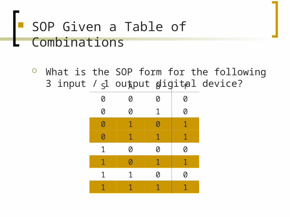
SOP Given a Table of Combinations
What is the SOP form for the following 3 input / 1 output digital device?
S A B f
0 0 0 0
0 0 1 0
0 1 0 1
0 1 1 1
1 0 0 0
1 0 1 1
1 1 0 0
1 1 1 1
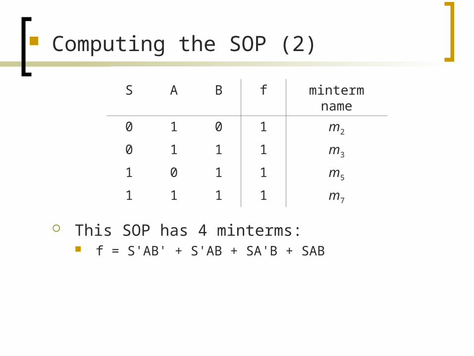
Computing the SOP (2)
This SOP has 4 minterms: f = S'AB' + S'AB + SA'B + SAB
S A B f minterm name
0 1 0 1 m2
0 1 1 1 m3
1 0 1 1 m5
1 1 1 1 m7

Canonical SOP
Boolean functions can use shorthand notation when in SOP form: f = S'AB' + S'AB + SA'B + SAB
f(S,A,B) = (m2,m3,m5,m7)
or
f(S,A,B) = m(2,3,5,7)
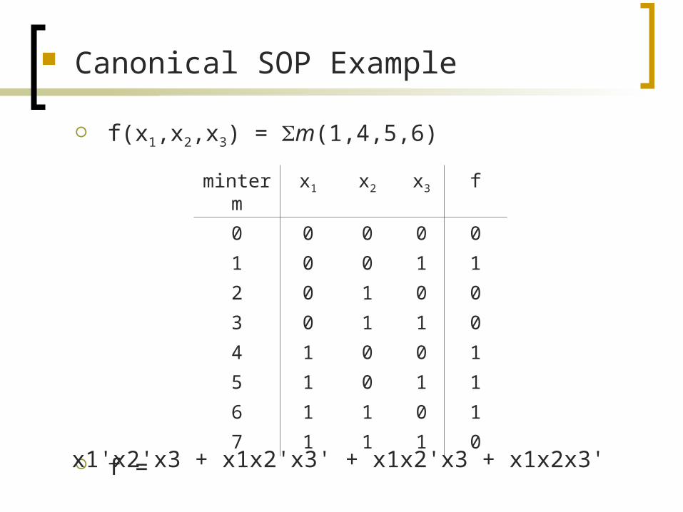
Canonical SOP Example
f(x1,x2,x3) = m(1,4,5,6)
f =
minterm x1 x2 x3 f
0 0 0 0 0
1 0 0 1 1
2 0 1 0 0
3 0 1 1 0
4 1 0 0 1
5 1 0 1 1
6 1 1 0 1
7 1 1 1 0
x1'x2'x3 + x1x2'x3' + x1x2'x3 + x1x2x3'
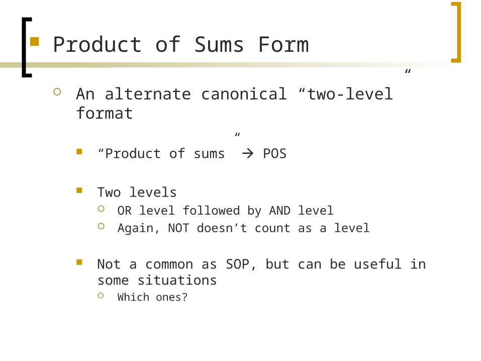
Product of Sums Form
An alternate canonical “two-level” format
“Product of sums” POS
Two levels OR level followed by AND level Again, NOT doesn’t count as a level
Not a common as SOP, but can be useful in some situations Which ones?

Computing the POS
Identify rows with “0” on output (f = 0)
Represent the input for each 0 row as a maxterm A logical “sum” of the input bits which guarantees that term
will be “0” (sum of literals)
A B f
0 0 0
0 1 1
1 0 0
1 1 0
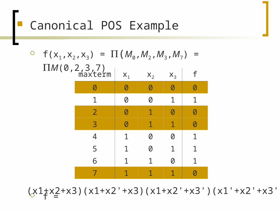
Canonical POS Example
f(x1,x2,x3) = (M0,M2,M3,M7) = M(0,2,3,7)
f =
maxterm x1 x2 x3 f
0 0 0 0 0
1 0 0 1 1
2 0 1 0 0
3 0 1 1 0
4 1 0 0 1
5 1 0 1 1
6 1 1 0 1
7 1 1 1 0
(x1+x2+x3)(x1+x2'+x3)(x1+x2'+x3')(x1'+x2'+x3')
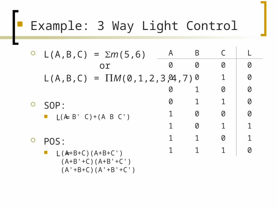
Example: 3 Way Light Control
L(A,B,C) = m(5,6)or
L(A,B,C) = M(0,1,2,3,4,7)
SOP: L =
POS: L =
A B C L
0 0 0 0
0 0 1 0
0 1 0 0
0 1 1 0
1 0 0 0
1 0 1 1
1 1 0 1
1 1 1 0
(A B' C)+(A B C')
(A+B+C)(A+B+C')(A+B'+C)(A+B'+C')(A'+B+C)(A'+B'+C')
Question:
Under what conditions would POS form be better? (assuming we aren’t doing further reductions)

Inverters in Two-Level Circuits
Inverters are not always required for two-level logic This is why we do not always count them among the cost of
a circuit
Later, we will see that many variables will be available to us in both normal and inverted form don't need to invert them
We show them only for completeness at this point

NAND/NOR Circuits

Completeness of NAND
Any Boolean function can be implemented using just NAND gates. Why? Need AND, OR, and NOT NOT: 1-input NAND (or 2-input NAND with inputs
tied together) AND: NAND followed by NOT OR: NAND preceded by NOTs
Likewise for NOR
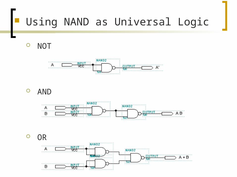
Using NAND as Universal Logic
NOT
AND
OR
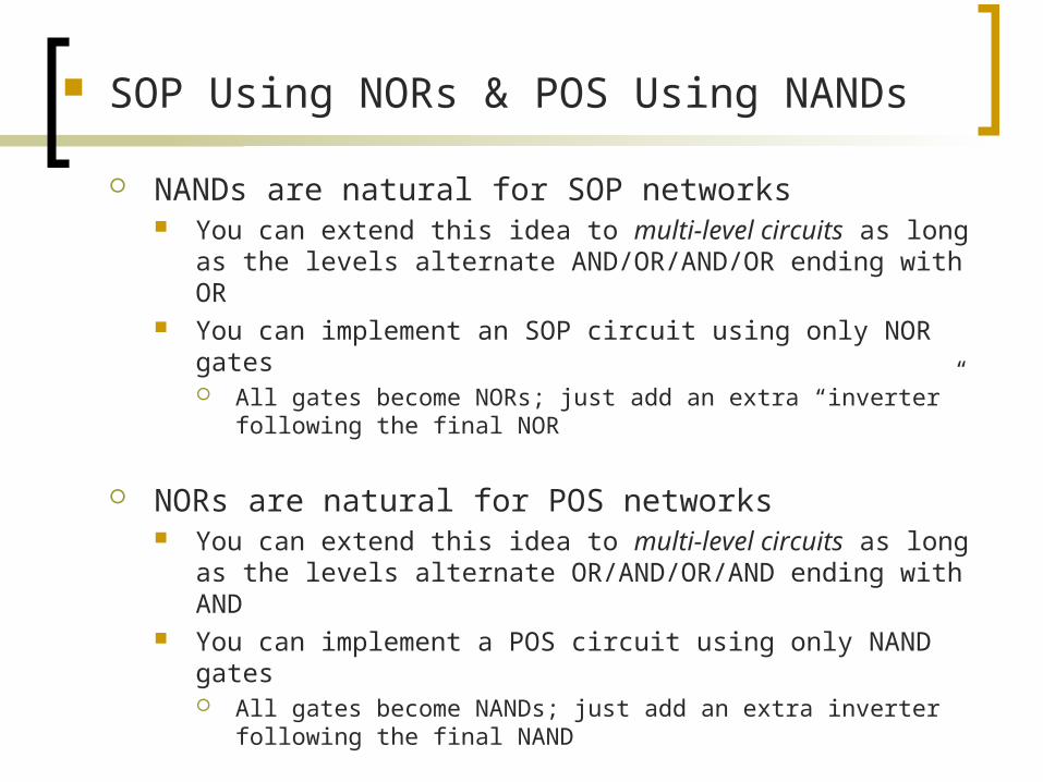
SOP Using NORs & POS Using NANDs
NANDs are natural for SOP networks You can extend this idea to multi-level circuits as long as
the levels alternate AND/OR/AND/OR ending with OR You can implement an SOP circuit using only NOR gates
All gates become NORs; just add an extra “inverter” following the final NOR
NORs are natural for POS networks You can extend this idea to multi-level circuits as long as
the levels alternate OR/AND/OR/AND ending with AND You can implement a POS circuit using only NAND gates
All gates become NANDs; just add an extra inverter following the final NAND
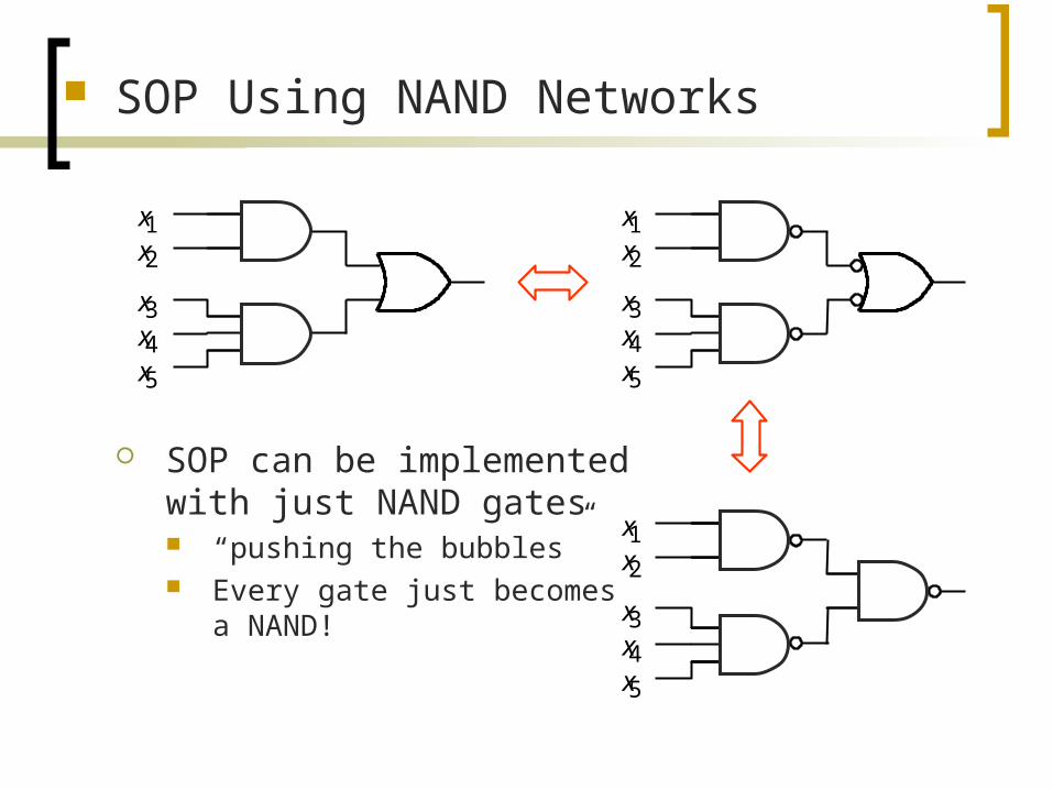
SOP Using NAND Networks
SOP can be implementedwith just NAND gates “pushing the bubbles” Every gate just becomes
a NAND!
x 1 x 2
x 3 x 4 x 5
x 1 x 2
x 3 x 4 x 5
x 1 x 2
x 3 x 4 x 5
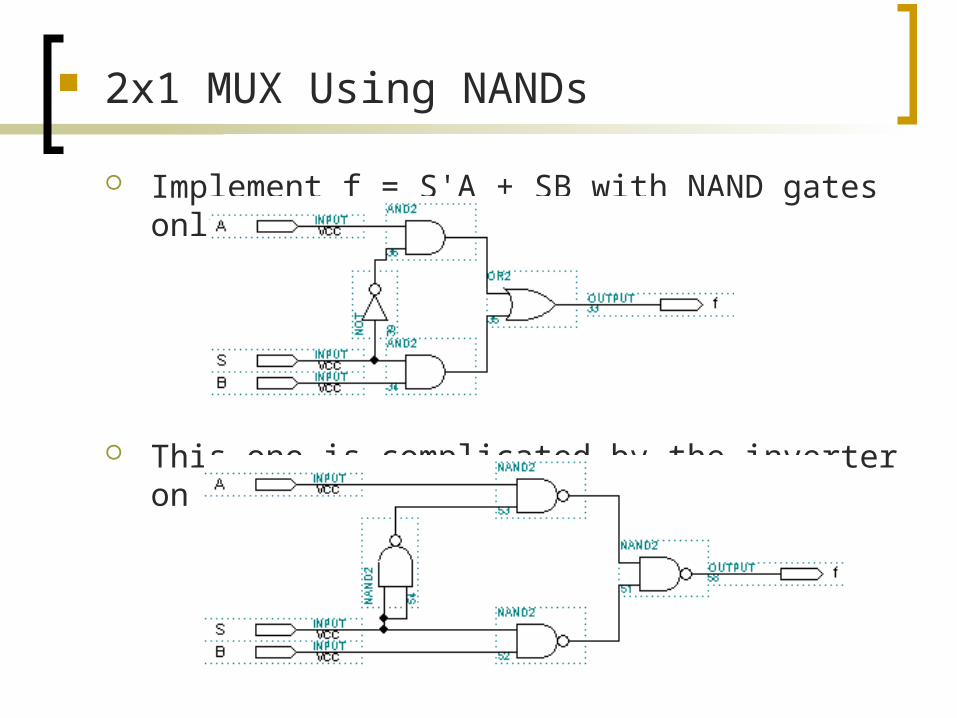
2x1 MUX Using NANDs
Implement f = S'A + SB with NAND gates only
This one is complicated by the inverter on S!

POS Using NOR Networks
POS can be implementedwith just NOR gates Every gate just becomes
a NOR
x 1
x 2
x 3
x 4
x 5
x 1
x 2
x 3
x 4
x 5
x 1
x 2
x 3
x 4
x 5

Schematics of DeMorgan’s Laws
(x ∙ y)' = x' + y'
(x + y)' = x' ∙ y'

Universal Logic Families
Any logic function can be designed using only:
AND, OR, NOT NAND NOR
These are called “universal logic families”
Actual components are often designed using either NAND or NOR gates only NAND and NOR require fewer transistors to build Just having a single gate design is simpler than having 3!

AND/OR Networks NAND/NAND
Convert multi-level AND/OR net NAND/NAND
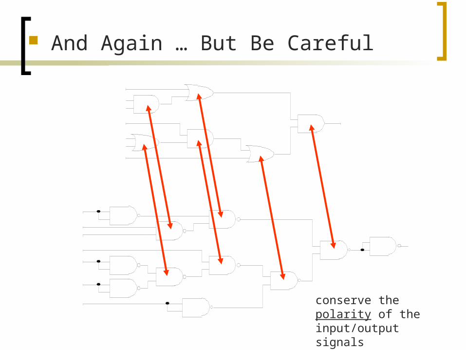
And Again … But Be Careful
conserve the polarity of the input/output signals
Some Useful Circuits

Decoders and Multiplexors
Decoder: Popular combinational logic building block, in addition to logic gates Converts input binary number
to one high output 2-input decoder: four possible
input binary numbers So has four outputs, one for
each possible input binary number
Internal design AND gate for each output to
detect input combination Decoder with enable e
Outputs all 0 if e=0 Regular behavior if e=1
n-input decoder: 2n outputs
i0
i1
d0
d1
d2
d3 1
1
1
0
0
0
i0
i1
d0
d1
d2
d3 0
0
0
0
0
1
i0
i1
d0
d1
d2
d3
i0
i1
d0
d1
d2
d30
0
1
0
1
0
0
1
0
1
0
0
i0
d0
d1
d2
d3
i1
i0
i1
d0
d1
d2
d3e 1
1
1
1
0
0
0
e
i0
i1
d0
d1
d2
d3 0
1
1
0
0
0
0
i1’i0’
i1’i0
i1i0’
i1i0

Multiplexor (Mux) Mux: Another popular combinational building block
Routes one of its N data inputs to its one output, based on binary value of select inputs 4 input mux needs 2 select inputs to indicate which input to route
through 8 input mux 3 select inputs N inputs log2(N) selects
Like a railyard switch
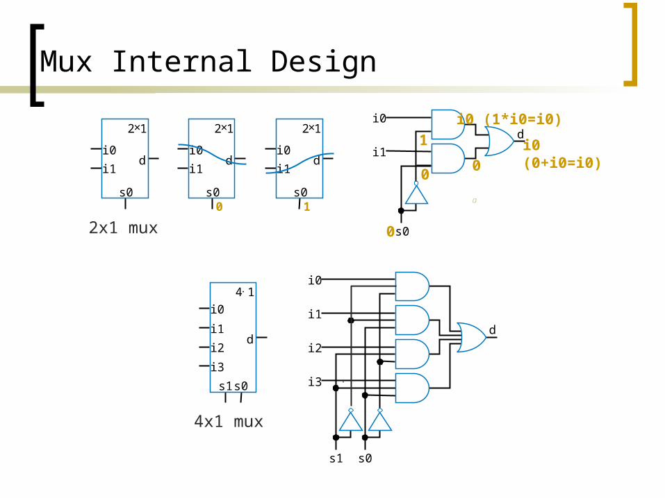
Mux Internal Design
s0
di0
i1
2×1
i1
i0
s01
d
2×1
i1
i0
s00
d
2×1
i1
i0
s0
d
0
i0 (1*i0=i0)
i0(0+i0=i0)
1
0
2x1 mux
i041
i2
i1
i3
s1s0
d
s0
d
i0
i1
i2
i3
s1
4x1 mux
0
a
Muxes Commonly Together -- N-bit Mux
Ex: Two 4-bit inputs: A (a3 a2 a1 a0) and B (b3 b2 b1 b0) 4-bit 2x1 mux (just four 2x1 muxes sharing a select line) can select
between A or B
i0
s0i1
21d
i0
s0i1
21d
i0
s0i1
21d
i0
s0i1
21d
a3b3
I0
s0
s0
I1
4-bit2x1
D CA
B
a2b2
a1b1
a0b0
s0
4C
44
4
c3
c2
c1
c0
is shortfor
Simplifyingnotation:

N-bit Mux Example
Four possible display items Temperature (T), Average miles-per-gallon (A), Instantaneous mpg (I),
and Miles remaining (M) -- each is 8-bits wide Choose which to display using two inputs x and y Use 8-bit 4x1 mux