novel approach to analyze transients in shipboard … electric power distribution architectures for...
TRANSCRIPT
FACHHOCHSCHUL - MASTERSTUDIENGANG
AUTOMATISIERUNGSTECHNIK
Novel Approach to AnalyzeTransients in Shipboard PowerSystems Based on Scattering
Parameters Modeling
RESEARCH PAPER
by
MATTHIAS KOFLER BSc
5. March - 5. October
Assistance of the Research by
Prof. (FH) Univ. Doz. Dipl.-Ing. Dr. Karl Heinz Kellermayr
Dr. Lukas Graber
Acknowledgement
The Center for Advanced Power Systems (CAPS) is a state-of-the-art research facil-ity of the Florida State University and possesses the reputation in doing outstandingresearch in the field of power systems technology. I have learned a lot throughout mystay at CAPS, with many challenging yet valuable experiences in order to completethis work. This would not have been possible without the help of many people whyI want to use this portion of my thesis to mention all those who helped me with myresearch project.
First I would like to thank Dr. Michael „Mischa“ Steuer who has given me the oppor-tunity to accomplish my project in the Power Systems Group at CAPS and withoutwhom this thesis would not have been possible at all. I would also like to expressmy gratitude to my supervisor Dr. Lukas Graber who helped me throughout theprocess obtaining my project and who made working on this thesis very manageableand a great learning experience due to his congenial and easily approachable nature,along with being a pool of knowledge.
Thanks also goes to my supervisor in Austria Prof. (FH) Univ. Doz. Dipl.-Ing. Dr. KarlHeinz Kellermayr from University of Applied Sciences Upper Austria who was verysupportive, helpful and guided me really well from the beginning of this projectuntil its completion beside from CAPS. I benefited significantly from the feedbackand suggestions of my supervisors not only in technical terms but also in regard topreparing this paper.
I would also like to thank Dr. William Brey from the National High Magnetic FieldLaboratory for providing the equipment and assistance required for doing the mea-surements needed.
I also want to thank Dipl.-Kulturw. Vanessa Prüller from the international officeat my home university for her support with the international affairs to enable theaccomplishment of the internship at CAPS. Further, I want to thank the AustrianMarshallplan Foundation as I did the research for this Master Thesis as a scholarfrom the Austrian Marshallplan Foundation.
I

Last but not least, I would like to thank my family for supporting me during mypresence as a student and everyone else who has been involved in my project in oneway or another.
This work was supported by the United States Office of Naval Research (ONR)under Grant No. N00014-04-1-0664.
II
Abstract
The research presented in this thesis have been performed in 2012 at the Center forAdvanced Power Systems (CAPS) of the Florida State University (FSU). Topic ofresearch is the concept for the future All Electrical Ship (AES) of the U.S. Navy.
Primary focus of this thesis is on a novel approach on modeling and simulation ofelectrical power supply system components using Scattering parameters (S-parameters)for the analysis of different system grounding architectures.
In chapter 1 and 2 a short introduction to the AES concept and the topic of powersystem grounding is given, while in chapter 3 the modeling approach based onS-parameters is presented. This approach allows the modeling of power systemcomponents such as cables, bus bars, machines, power electronic converters andthe ship hull based on generated or measured S-parameters for the development ofsimulation models. These models can be used to perform simulation studies.
The S-parameter approach is a novelty in the field of power simulations. Availablesimulation software packages for power system modeling such as PSCAD/EMTDCor MATLAB/Simulink usually do not allow to directly integrate linear networkblocks characterized by S-parameters. A generic N-port block has been developedwhich allows to embed models of subsystems based on their S-parameter in powersystems software packages in the manner of linear time invariant (LTI) networks.
The model implementation is presented and validation studies have been performedwhich show good modeling performance. As a result of the research, investigationscan now be performed for studying the experimental power system setup of PurdueUniversity to support the development of the AES.
III
Executive Summary
This master thesis is result of an internship at the Center for Advanced PowerSystems (CAPS). CAPS is a research facility of the Florida State University and oneof the major partners in the Electric Ship Research and Development Consortium(ESRDC) of the United States Office of Naval Research (ONR). The focus of theresearch described in this thesis is on the topic of grounding for an all-electric shippower system. It is part of an ongoing research project in the ESRDC with the aimto support the development of next-generation all-electric naval ships. These referto ships whose power generation, propulsion and auxiliary systems entirely dependon electric power. Further, these ships employ new ship designs and have the abilityto make use of advanced weaponry.
Presently, three main systems are being considered which may have application indifferent future ship types associated to the U.S. Navy. Of all three architecturesdefined, the direct current (DC) system, operated at medium voltage (MVDC) ispredicted to be most appropriate power distribution system for future’s naval all-electric warships. As with any power distribution architecture, there are numeriousdesign considerations that need to be addressed. One issue that has been raised inthe design of MVDC power systems is the topic of grounding. This topic is part ofthe recommended practice for MVDC ship power systems. The system groundinghas significant impact on a ship as to personnel safety, survivability and continuityof the electrical power supply. While the grounding practices of AC shipboard powersystems are generally well resolved, there is very little literature available and evenfewer guidance given how to engineer grounding for DC power systems on ships.Further, there are no vetted approaches to the analysis required to fully understandall the effects of engineered grounding systems on the performance of MVDC systemson ships. Therefore, the focus research in the field of power systems groundingconducted by the ESRDC is on grounding aspects related to this architecture andits conceptual features.
Ongoing research in the ESRDC studies different grounding schemes of DC ship-board power systems and their impacts on voltage transients, bus harmonics, fault
IV
current levels or power loss. One of the research thrusts of shipboard groundingis the transient behavior of the DC bus voltage as a function fo the location of aprospective single rail-to-ground fault. Circuit simulation software allows modelingof shipboard power systems and helps to analyze the characteristics of transients fora certain grounding scheme. Recent studies have shown, that in such a fault scenarionot only a static response but also a high frequency transient phenomena can beobserved. The exact shape of this transients depends on high frequency characteris-tics of all components including the DC distribution bus. Models are required whichare suitable to simulate fast transients as the can occur in shipboard power systemswith high power density, short line lengths and low damping characteristics. Recentstudies have shown that simulations models based on lumped elements have onlylimited capabilities to accurately model high-frequency transients. Such models donot include effects of travelling wave propagation and reflection. A completely newapproach had to be developed.
Based on these studies the characterization of power systems components basedon Scattering parameters (S-parameters) has been initiated. The S-parameter ap-proach is not common in power systems and hence a novelty in the field of powersimulations. Therefore, the aim is to develop models of subsystems and deter-mine their S-parameters. In particular this work focus on embedding S-parametersin models of shipboard power systems with emphasis on the implementation inSimulink/SimPowerSystems. Simulation software packages routinely used in ES-RDC activities for shipboard power systems simulations such as PSCAD/EMTDCor MATLAB/Simulink do not allow to directly integrate linear network blocks char-acterized by S-parameters. This is in contrast to software packages commonly usedin the high-frequency engineering in which S-parameter blocks tpyically innatelyavailable.
A generic N-port block has been developed which allows to embed models of subsys-tems based on their S-parameter in power systems software packages in the mannerof linear time invariant (LTI) networks. Validation of this implementation has beenconducted using Agilent Advanced Design System (ADS). A. linear time-invariantnetworks have been defined by circuits using passive lumped elements. The samecircuit has been implemented in SimPowerSystems by its S-parameter and the andthe step response recorded. An overlay of the results shows a perfect agreement.It turned out that the accuracy of the S-parameter implementation is qualified forhigh-fidelity power systems simulations.
Purdue University, another member of the ESRDC built a small-scale testbed to
V

study the performance of different grounding schemes proposed for MVDC powersystems. A complete S-parameters characterization of the power electronics com-ponents incorporated has been conducted. The measurements were carried outin collaboration with the National High Magnetic Field Laboratory (NHMFL) bymeans of a 2-port vector network analyzer (VNA). MATLAB tools and scripts havebeen established which support the overall S-parameters approach. As a result ofthe research, investigations can now be performed for studying the experimentalpower system setup of Purdue University to support the development of the AES.
VI
Inhaltsverzeichnis
Inhaltsverzeichnis VII
1 All-Electric-Ship Concept For Future’s Naval Vessels 1
1.1 All-Electric-Ship (AES) . . . . . . . . . . . . . . . . . . . . . . . . . . 1
1.2 Electric Power Distribution Architectures For Future Naval Ships . . 6
1.3 Shipboard Grounding Schemes . . . . . . . . . . . . . . . . . . . . . . 8
2 Grounding Schemes for MVDC Power Systems 9
3 Modeling of Power Systems Components 13
3.1 General Aspects of Modeling . . . . . . . . . . . . . . . . . . . . . . . 13
3.2 S-Parameters as Modeling Approach for Multiport Networks . . . . . 14
3.3 Measurement of Scattering Parameters of an N-port Network . . . . . 19
3.3.1 Vector Network Analyzer . . . . . . . . . . . . . . . . . . . . . 19
3.3.2 Multiport Measurement by Means of a Two-Port Vector Net-work Analyzer . . . . . . . . . . . . . . . . . . . . . . . . . . . 22
3.3.3 Measurement of Purdue’s Small Scale Testbed Components . . 24
3.4 Model Implementation and Validation . . . . . . . . . . . . . . . . . 28
3.4.1 Model Implementation . . . . . . . . . . . . . . . . . . . . . . 28
3.4.1.1 Rational Function Modeling and Fitting . . . . . . . 29
3.4.1.2 Generation of Transfer Function Blocks . . . . . . . 31
3.4.1.3 Circuit Level Model Implementation . . . . . . . . . 33
3.4.2 Model Validation . . . . . . . . . . . . . . . . . . . . . . . . . 34
VII
INHALTSVERZEICHNIS
3.5 Circuit Simulations . . . . . . . . . . . . . . . . . . . . . . . . . . . . 37
3.5.1 3-Pi-Section Model . . . . . . . . . . . . . . . . . . . . . . . . 37
3.5.2 DC/DC Converter Model . . . . . . . . . . . . . . . . . . . . 40
3.6 Solver Settings and Pitfalls . . . . . . . . . . . . . . . . . . . . . . . . 42
4 Conclusion 45
List of Figures 48
List of Tables 51
Bibliography 52
A Archiving 56
B Matlab Tools 58
B.1 Main GUI . . . . . . . . . . . . . . . . . . . . . . . . . . . . . . . . . 58
B.2 Rational Fitting for S-parameters Transfer Functions . . . . . . . . . 59
B.3 Graphical Representation of S-parameters . . . . . . . . . . . . . . . 61
B.4 Generation of Touchstone File . . . . . . . . . . . . . . . . . . . . . . 63
B.5 N-Port S-Matrix Assembling . . . . . . . . . . . . . . . . . . . . . . . 65
C S-parameters Model Desription 67
D Multiport Characterization using a Two-Port Network Analyzer 71
D.1 3-port Network Measurements . . . . . . . . . . . . . . . . . . . . . . 71
D.2 4-port Network Measurements . . . . . . . . . . . . . . . . . . . . . . 72
D.3 5-port Network Measurements . . . . . . . . . . . . . . . . . . . . . . 73
D.4 6-port Network Measurements . . . . . . . . . . . . . . . . . . . . . . 74
VIII
1 All-Electric-Ship Concept ForFuture’s Naval Vessels
1.1 All-Electric-Ship (AES)
In recent years, the United States Navy began to reconsider the concept of traditionalnaval ship systems as a consequence of growing costs and military capabilities withthe goal to make ships more efficient and affordable by exploring new and morereconfigurable system architectures.
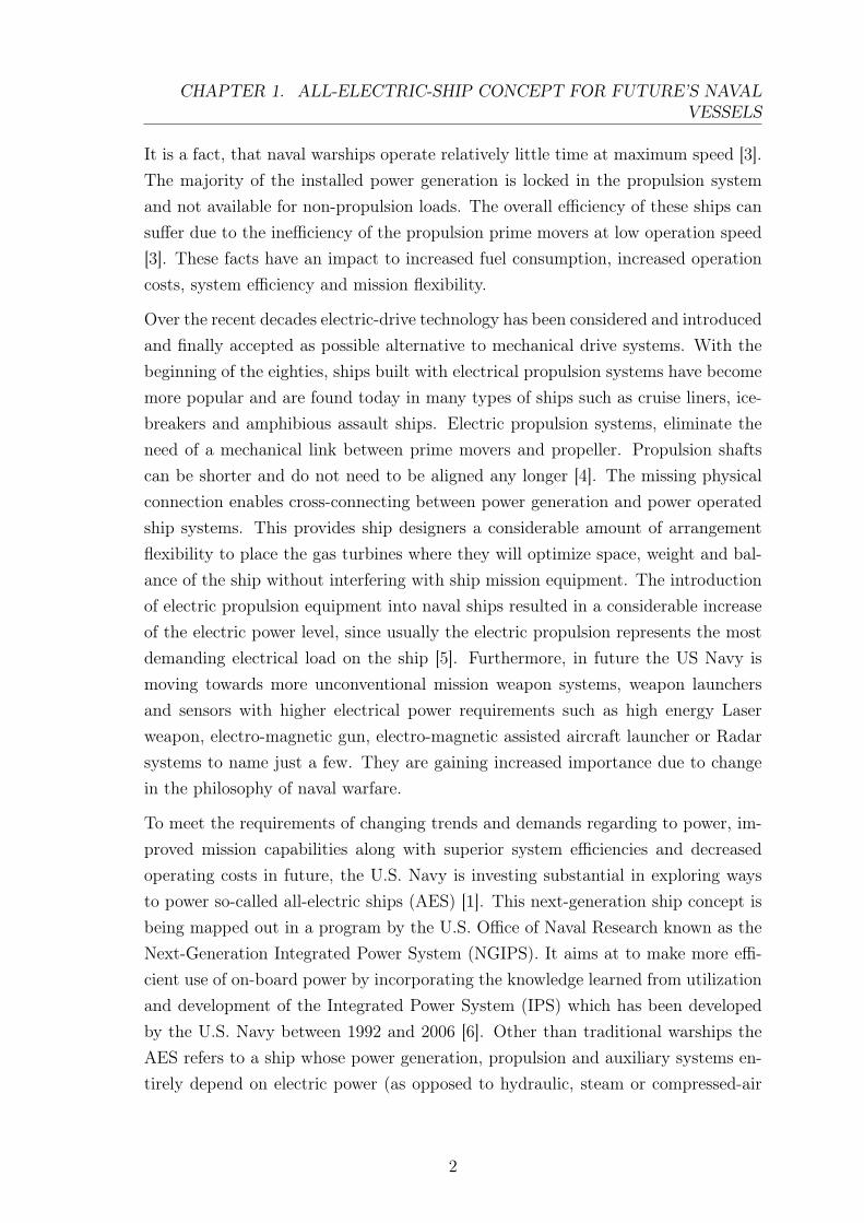
Conventional naval ships employ geared mechanical drive systems for propulsion.These ships host two separate sets of engines to provide the necessary energy forship propulsion and service loads [1]. One set of engines is directly-linked to themechanical propulsion system since a large amount of installed power is dedicatedto the propulsion [2]. Typically this set contains two pairs of gas turbines as theprime movers whereby each pair is connected to a large common reduction gearbox toreduce the engine’s high rotational-speed and to permit the operation of the propellerat lower rotational speeds. For survivability reasons one drive train must be locatedforward and the other aft. As a result, long line shafts of the propulsion systemare running through the ship to connect the gearboxes and rotate the propellers.Furthermore, the propellers location defines the centerline of the shaft lines andhence the vertical position of the prime movers. The required location as well asthe size and number of the installed machinery of the mechanical propulsion systemare considerable factors which reduce the internal space available for equipmentother than propulsion, prohibit efficient use of capacity, and restrict ship designersin their design flexibility. It might be fair to say the rest of the ship needs to bearranged and designed around these set of engines instead of creating a customizedpropulsion system for the ship. A second set, typically including three gas turbines,is connected to smaller auxiliary generators to operate all the electrically poweredequipment on these ships.
1
CHAPTER 1. ALL-ELECTRIC-SHIP CONCEPT FOR FUTURE’S NAVALVESSELS
It is a fact, that naval warships operate relatively little time at maximum speed [3].The majority of the installed power generation is locked in the propulsion systemand not available for non-propulsion loads. The overall efficiency of these ships cansuffer due to the inefficiency of the propulsion prime movers at low operation speed[3]. These facts have an impact to increased fuel consumption, increased operationcosts, system efficiency and mission flexibility.
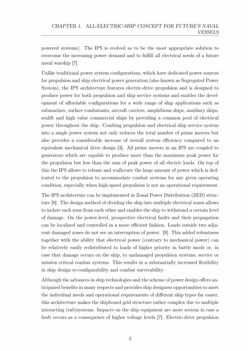
Over the recent decades electric-drive technology has been considered and introducedand finally accepted as possible alternative to mechanical drive systems. With thebeginning of the eighties, ships built with electrical propulsion systems have becomemore popular and are found today in many types of ships such as cruise liners, ice-breakers and amphibious assault ships. Electric propulsion systems, eliminate theneed of a mechanical link between prime movers and propeller. Propulsion shaftscan be shorter and do not need to be aligned any longer [4]. The missing physicalconnection enables cross-connecting between power generation and power operatedship systems. This provides ship designers a considerable amount of arrangementflexibility to place the gas turbines where they will optimize space, weight and bal-ance of the ship without interfering with ship mission equipment. The introductionof electric propulsion equipment into naval ships resulted in a considerable increaseof the electric power level, since usually the electric propulsion represents the mostdemanding electrical load on the ship [5]. Furthermore, in future the US Navy ismoving towards more unconventional mission weapon systems, weapon launchersand sensors with higher electrical power requirements such as high energy Laserweapon, electro-magnetic gun, electro-magnetic assisted aircraft launcher or Radarsystems to name just a few. They are gaining increased importance due to changein the philosophy of naval warfare.
To meet the requirements of changing trends and demands regarding to power, im-proved mission capabilities along with superior system efficiencies and decreasedoperating costs in future, the U.S. Navy is investing substantial in exploring waysto power so-called all-electric ships (AES) [1]. This next-generation ship concept isbeing mapped out in a program by the U.S. Office of Naval Research known as theNext-Generation Integrated Power System (NGIPS). It aims at to make more effi-cient use of on-board power by incorporating the knowledge learned from utilizationand development of the Integrated Power System (IPS) which has been developedby the U.S. Navy between 1992 and 2006 [6]. Other than traditional warships theAES refers to a ship whose power generation, propulsion and auxiliary systems en-tirely depend on electric power (as opposed to hydraulic, steam or compressed-air
2
CHAPTER 1. ALL-ELECTRIC-SHIP CONCEPT FOR FUTURE’S NAVALVESSELS
powered systems). The IPS is evolved as to be the most appropriate solution toovercome the increasing power demand and to fulfill all electrical needs of a futurenaval warship [7].
Unlike traditional power system configurations, which have dedicated power sourcesfor propulsion and ship electrical power generation (also known as Segregated PowerSystem), the IPS architecture features electric-drive propulsion and is designed toproduce power for both propulsion and ship service systems and enables the devel-opment of affordable configurations for a wide range of ship applications such assubmarines, surface combatants, aircraft carriers, amphibious ships, auxiliary ships,sealift and high value commercial ships by providing a common pool of electricalpower throughout the ship. Combing propulsion and electrical ship service systeminto a single power system not only reduces the total number of prime movers butalso provides a considerable increase of overall system efficiency compared to anequivalent mechanical drive design [3]. All prime movers in an IPS are coupled togenerators which are capable to produce more than the maximum peak power forthe propulsion but less than the sum of peak power of all electric loads. On top ofthis the IPS allows to release and reallocate the large amount of power which is ded-icated to the propulsion to accommodate combat systems for any given operatingcondition, especially when high-speed propulsion is not an operational requirement.
The IPS architecture can be implemented in Zonal Power Distribution (ZED) struc-ture [8]. The design method of dividing the ship into multiple electrical zones allowsto isolate each zone from each other and enables the ship to withstand a certain levelof damage. On the power-level, prospective electrical faults and their propagationcan be localized and controlled in a more efficient fashion. Loads outside two adja-cent damaged zones do not see an interruption of power. [9]. This added robustnesstogether with the ability that electrical power (contrary to mechanical power) canbe relatively easily redistributed to loads of higher priority in battle mode or, incase that damage occurs on the ship, to undamaged propulsion systems, service ormission critical combat systems. This results in a substantially increased flexibilityin ship design re-configurability and combat survivability.
Although the advances in ship technologies and the scheme of power design offers an-ticipated benefits in many respects and provides ship designers opportunities to meetthe individual needs and operational requirements of different ship types far easier,this architecture makes the shipboard grid structure rather complex due to multipleinteracting (sub)systems. Impacts on the ship equipment are more serious in case afault occurs as a consequence of higher voltage levels [7]. Electric-drive propulsion
3
CHAPTER 1. ALL-ELECTRIC-SHIP CONCEPT FOR FUTURE’S NAVALVESSELS
equipment might be larger and heavier compared to equivalent mechanical-drivedevices. As with any industrial product, the component-level technology is movingtowards becoming smaller and lighter by being more energy efficient. It is expectedthat size and weight of electric-drive systems will come down over time to dimensionscomparable to mechanical drive systems. Nevertheless the merits of the integratedelectric-drive propulsion such as fuel savings can offset the size and weight drawbackalready today [1].
Figure 1.1 compares a conventional ship design with a design based on IPS. Althoughthis figure does not correspond to any real ship’s one-line diagram (multiple gen-erators, motors and conduction paths for reliability and survivability), it providesa basic understanding of the essential differences of a power system configurationsincluding mechanical ship propulsion compared to an integrated electric architec-ture. Even if commercial ships are already using electric propulsion the concept anddevelopment of a next generation naval ships based on AES is still in its infancy [1].The utilization of large power level generation and distribution on ships with theirsevere space constraints, poses new multidisciplinary challenges in ship design andmanufacturing.
As there are many uncertain parameters in many respects which need to be ad-dressed, the United States ONR1 established the Electric Ship Research and Devel-opment Consortium2 (ESRDC). ESRDC is a consortium of eight individual researchinstitutions with fundamental knowledge in the field of power systems technologyand focuses on research in electric ship concepts. These institutions are dedicatednot only to furthering research in electric ship and other advanced electric tech-nologies, but also to address the national shortage of electric power engineers byproviding educational opportunities.
1http://www.onr.navy.mil/2http://www.esrdc.com/
4
CHAPTER 1. ALL-ELECTRIC-SHIP CONCEPT FOR FUTURE’S NAVALVESSELS
Shaft With
Reduction Gear
Prime
Mover
Mech
anic
al
Pro
puls
ion
Prime
Mover
Propelle
r
Pow
er
Dis
trib
uti
on
G
PCM
SL
2.6
Auxiliary
Generators
PCM
SL
2.4
PCM
SL
2.1
SL
2.2
PCM
SL
2.3
PCM
SL
2.5
PCM
PCM
SL
2.7
SL
2.8
PCM
Prime
MoverG
PCM
SL
1.5
PCM
SL
1.3
PCM
SL
1.1
SL
1.2
PCM
SL
1.4
PCM
PCM
SL
1.6
SL
1.7
PCMService
Loads
(a) Conventional Ship Design showing prime movers, auxiliary generators, service loads (SL), andpower converter modules (PCM)
Propelle
r
(b) Electric Propulsion with Integrated Power
Figure 1.1: Simplified shipboard power system comparing a conventional design(above) with a design based on IPS (below) [4, modified]
5
CHAPTER 1. ALL-ELECTRIC-SHIP CONCEPT FOR FUTURE’S NAVALVESSELS
1.2 Electric Power Distribution Architectures For
Future Naval Ships
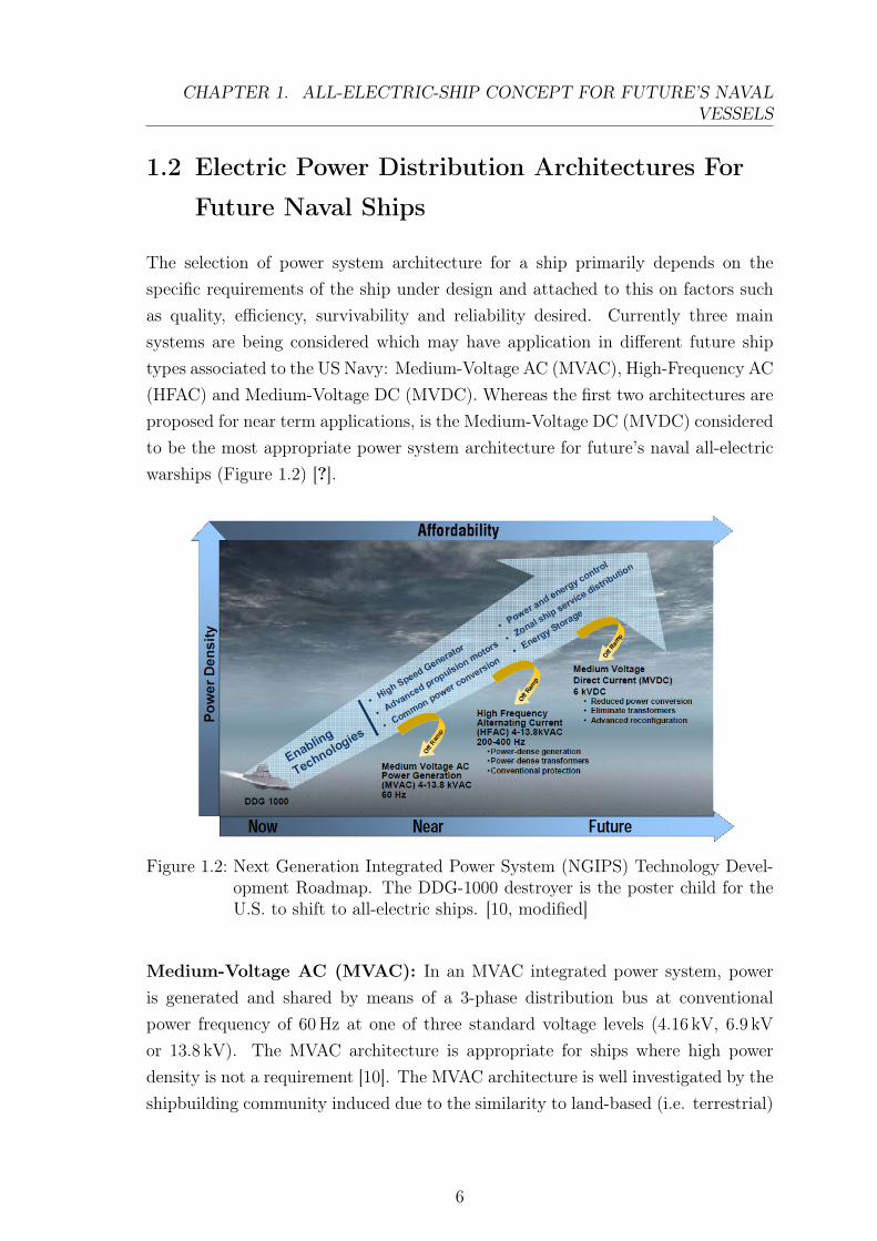
The selection of power system architecture for a ship primarily depends on thespecific requirements of the ship under design and attached to this on factors suchas quality, efficiency, survivability and reliability desired. Currently three mainsystems are being considered which may have application in different future shiptypes associated to the US Navy: Medium-Voltage AC (MVAC), High-Frequency AC(HFAC) and Medium-Voltage DC (MVDC). Whereas the first two architectures areproposed for near term applications, is the Medium-Voltage DC (MVDC) consideredto be the most appropriate power system architecture for future’s naval all-electricwarships (Figure 1.2) [?].
Figure 1.2: Next Generation Integrated Power System (NGIPS) Technology Devel-opment Roadmap. The DDG-1000 destroyer is the poster child for theU.S. to shift to all-electric ships. [10, modified]
Medium-Voltage AC (MVAC): In an MVAC integrated power system, poweris generated and shared by means of a 3-phase distribution bus at conventionalpower frequency of 60 Hz at one of three standard voltage levels (4.16 kV, 6.9 kV
or 13.8 kV). The MVAC architecture is appropriate for ships where high powerdensity is not a requirement [10]. The MVAC architecture is well investigated by theshipbuilding community induced due to the similarity to land-based (i.e. terrestrial)
6
CHAPTER 1. ALL-ELECTRIC-SHIP CONCEPT FOR FUTURE’S NAVALVESSELS
AC power distribution systems and thus can be deployed in the ship with limiteddevelopment effort.
High-Frequency AC (HFAC): Unlike the MVAC integrated power system, poweris generated at a fixed frequency at or above 200 Hz rather than 60 Hz but lessthan 400 Hz and hence referred to as the high frequency architecture. HFAC is anintermediate step towards the MVDC architecture and for ships with high powerdensity requirements. On one hand it provides several advantages compared toMVAC such as a reduction of size and weight of transformers and rotating machinery,improved acoustic performance or lower harmonic distortion. On the other hand,the higher frequency also introduces several challenges such as high number of polesbeing required for generators or prime movers are restricted to specific operatingspeeds [10].
Medium-Voltage DC (MVDC): The MVDC integrated power system is thetarget NGIPS architecture to meet the high power density requirements of futuresurface combatants and submarines. The primary difference on system-level com-pared to an (HF)AC power system is that power is generated as AC, but distributedas DC power through out the ship. Consequently a couple of conceptual featurescome along with this architecture. The prime movers speed is fully decoupled fromthe frequency of the main distribution bus which enables the possibilty to optimizethe generators for each type of prime movers without gears. Engineering concerns(e.g. cable installations) with respect to electromagnetic interference (EMI) andelectromagnetic compatibility (EMC) present with HFAC architecture are reduced.On system-level the DC system is simpler, since many conversion steps are avoided.Each step conversion causes losses and potentially reduces reliability of the system.Overall the MVDC architecture is predicted to provide the highest payoff by promis-ing highest capabilities at the least total cost of ownership. However, the applicationand conceptual changes of the MVDC architecture make this the technically mostchallenging one of all three architectures defined [10].
The pros and cons of the integrated power system architectures are described moredetailed in [10].
The architectures mentioned above have in common, that the choice of appropriategrounding schemes is of utmost importance for the performance of the power system.
7
CHAPTER 1. ALL-ELECTRIC-SHIP CONCEPT FOR FUTURE’S NAVALVESSELS
1.3 Shipboard Grounding Schemes
The grounding strategy of an electrical shipboard power distribution system is a ma-jor aspect since the primary objective is personel safety, availability and continuity(reliability) of the electrical power supply in case of a system fault. Traditionally,literature and especially established engineering practices, distinguish between un-grounded, impedance grounded (high or low impedance) and effectively groundedpower systems. Strictly speaking there are no ungrounded systems since there isalways some degree of parasitic coupling to ground present. Therefore, ungroundedsystems are also understood as parasitically or not intentionally grounded systems.For ships the unintentionally or high-impedance grounding schemes are preferredsince those allow to continue operation of all equipment throughout the ship in caseof a single-rail-to ground fault (without clearing the first ground fault exists) [11].But these grounding schemes come with their own set of issues. One problematicissue arises when locating such a fault since those do not provide considerable faultcurrents for tracing fault location.
Capacitive, resistive, and inductive grounding have specific characteristics whichneed to be carefully studied. Also the location of the engineered grounding pointhas substantial impact to the performance of the power system during normal op-eration and during faults. Despite the importance of the engineered grounding forshipboard electrical power systems the established practices [12] still rely on rathersimplified analytical approaches which have primarily been established and validatedfor terrestrial power systems [13]. While the grounding practices of AC shipboardpower systems are generally well resolved, there is very little literature available andeven fewer guidance given how to engineer grounding for DC power systems on ships[11].
Therefore, the focus research in the field of power systems grounding conductedby the Electric Ship research and development Consortium (ESRDC) is on ground-ing aspects of direct current (DC) systems, especially operated at medium voltage(MVDC).
8
2 Grounding Schemes for MVDCPower Systems
Unlike terrestrial distribution systems, shipboard power systems carry a couple ofunique features such as the presence hazardous conditions during missions, high re-quirements for reliability and the ability for continuity of operation during certainfault scenarios, low damping properties and significantly high power density dueto short cable lengths, wide spread use of power electronics devices and non-linearloads. Furthermore, the power distribution system of future electric ships will belikely different in contrast to terrestial systems, since its architecture is MVDC andfeatures a single service line for propulsion and service loads. Beside the increasedreconfiguration options to support maximum capability on the ship at all times, itresults in an increased adoption of power electronics and increased power demandsdue to electric propulsion system and pulsed loads [14]. The conceptual innovationattached to the MVDC distribution system raises numerous design considerationswhich need to be addressed in future. One key issue following the recommendedpractice for MVDC electrical shipboard power sytems and the unique features men-tioned above is the grounding strategy. The system grounding has significant impacton many facets of operation on the ship.
Ongoing research in the ESRDC studies different grounding schemes of DC ship-board power systems and their impacts on voltage transients, bus harmonics, faultcurrent levels or power loss. In [15] and [16] different grounding schemes and theirimpact to the ships power system as a function of the location of a prospectivesingle rail-to ground fault have been studied and the performance compared. Thegrounding schemes under consideration are: grounding at the DC midpoint (Vmid),grounding at the neutral point of the generator (Vn) and an ungrounded system.In this context the ship hull is assumed to be on one single ground potential. Fig-ure 2.1 shows a simplified DC power system of a more complex MVDC shipboardpower system topology often found in literature. The simplification is argued froma system ground prospective to be fully sufficient to gain insight into the grounding
9
CHAPTER 2. GROUNDING SCHEMES FOR MVDC POWER SYSTEMS
aspects related to the proposed grounding schemes.
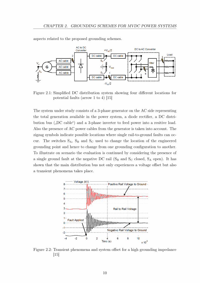
Figure 2.1: Simplified DC distribution system showing four different locations forpotential faults (arrow 1 to 4) [15]
The system under study consists of a 3-phase generator on the AC side representingthe total generation available in the power system, a diode rectifier, a DC distri-bution bus („DC cable“) and a 3-phase inverter to feed power into a resitive load.Also the presence of AC power cables from the generator is taken into account. Thezigzag symbols indicate possible locations where single rail-to-ground faults can oc-cur. The switches SA, SB and SC used to change the location of the engineeredgrounding point and hence to change from one grounding configuration to another.To illustrate on scenario the evaluation is continued by considering the presence ofa single ground fault at the negative DC rail (SB and SC closed, SA open). It hasshown that the main distribution bus not only experiences a voltage offset but alsoa transient phenomena takes place.
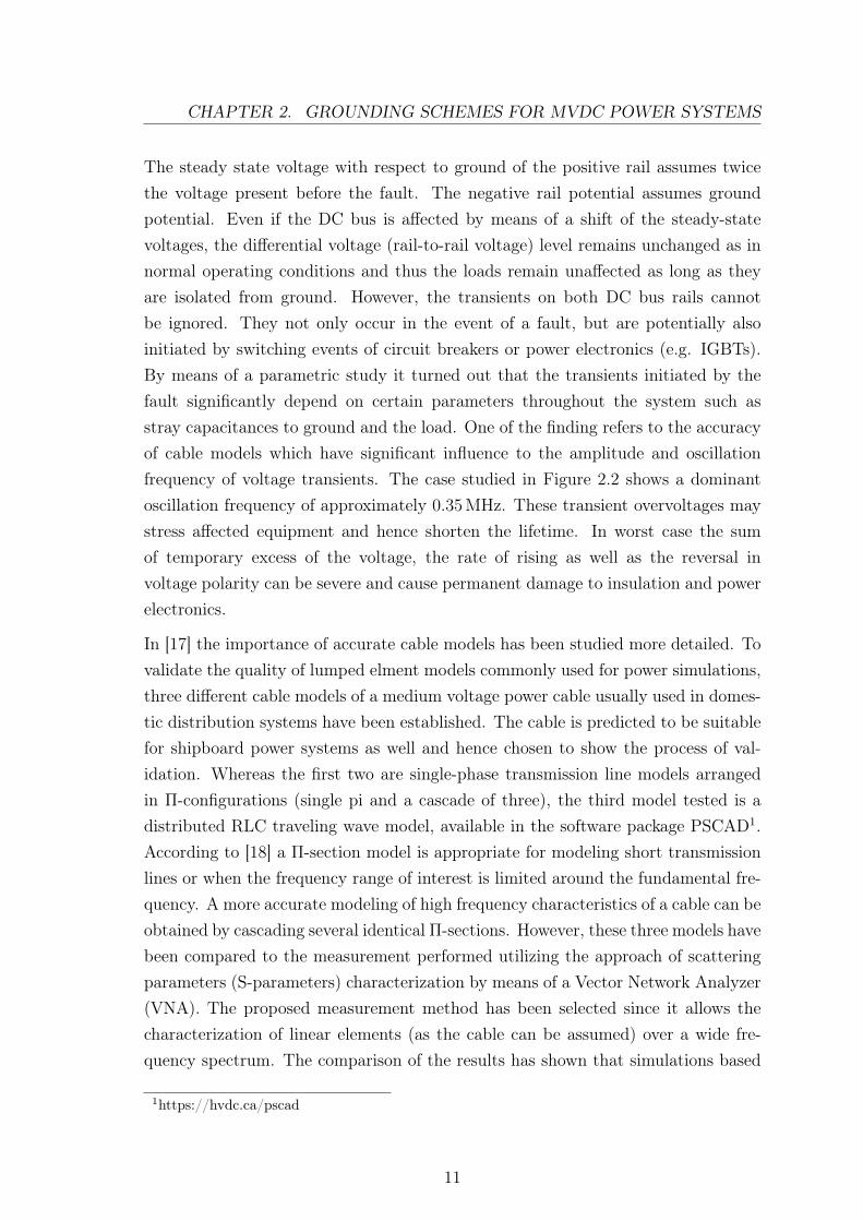
Figure 2.2: Transient phenomena and system offset for a high grounding impedance[15]
10
CHAPTER 2. GROUNDING SCHEMES FOR MVDC POWER SYSTEMS
The steady state voltage with respect to ground of the positive rail assumes twicethe voltage present before the fault. The negative rail potential assumes groundpotential. Even if the DC bus is affected by means of a shift of the steady-statevoltages, the differential voltage (rail-to-rail voltage) level remains unchanged as innormal operating conditions and thus the loads remain unaffected as long as theyare isolated from ground. However, the transients on both DC bus rails cannotbe ignored. They not only occur in the event of a fault, but are potentially alsoinitiated by switching events of circuit breakers or power electronics (e.g. IGBTs).By means of a parametric study it turned out that the transients initiated by thefault significantly depend on certain parameters throughout the system such asstray capacitances to ground and the load. One of the finding refers to the accuracyof cable models which have significant influence to the amplitude and oscillationfrequency of voltage transients. The case studied in Figure 2.2 shows a dominantoscillation frequency of approximately 0.35 MHz. These transient overvoltages maystress affected equipment and hence shorten the lifetime. In worst case the sumof temporary excess of the voltage, the rate of rising as well as the reversal involtage polarity can be severe and cause permanent damage to insulation and powerelectronics.
In [17] the importance of accurate cable models has been studied more detailed. Tovalidate the quality of lumped elment models commonly used for power simulations,three different cable models of a medium voltage power cable usually used in domes-tic distribution systems have been established. The cable is predicted to be suitablefor shipboard power systems as well and hence chosen to show the process of val-idation. Whereas the first two are single-phase transmission line models arrangedin Π-configurations (single pi and a cascade of three), the third model tested is adistributed RLC traveling wave model, available in the software package PSCAD1.According to [18] a Π-section model is appropriate for modeling short transmissionlines or when the frequency range of interest is limited around the fundamental fre-quency. A more accurate modeling of high frequency characteristics of a cable can beobtained by cascading several identical Π-sections. However, these three models havebeen compared to the measurement performed utilizing the approach of scatteringparameters (S-parameters) characterization by means of a Vector Network Analyzer(VNA). The proposed measurement method has been selected since it allows thecharacterization of linear elements (as the cable can be assumed) over a wide fre-quency spectrum. The comparison of the results has shown that simulations based
1https://hvdc.ca/pscad
11
CHAPTER 2. GROUNDING SCHEMES FOR MVDC POWER SYSTEMS
on simple lumped element models have limited capabilities to accurately model andrepresent high frequency transient phenomena due to traveling wave propagationsand reflections in cables. Referring to this, the authors conclude, that the proposedmethod of using S-parameters is an efficient and accurate way to characterize anylinear device within a particular frequency range of interest.
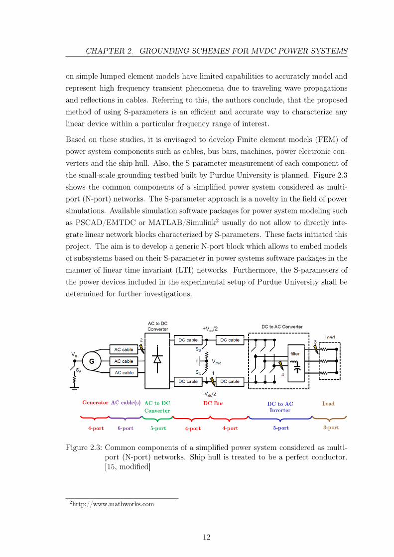
Based on these studies, it is envisaged to develop Finite element models (FEM) ofpower system components such as cables, bus bars, machines, power electronic con-verters and the ship hull. Also, the S-parameter measurement of each component ofthe small-scale grounding testbed built by Purdue University is planned. Figure 2.3shows the common components of a simplified power system considered as multi-port (N-port) networks. The S-parameter approach is a novelty in the field of powersimulations. Available simulation software packages for power system modeling suchas PSCAD/EMTDC or MATLAB/Simulink2 usually do not allow to directly inte-grate linear network blocks characterized by S-parameters. These facts initiated thisproject. The aim is to develop a generic N-port block which allows to embed modelsof subsystems based on their S-parameter in power systems software packages in themanner of linear time invariant (LTI) networks. Furthermore, the S-parameters ofthe power devices included in the experimental setup of Purdue University shall bedetermined for further investigations.
5-port 4-port 5-port4-port6-port 3-port4-port
AC to DC
Converter
DC Bus DC to AC Inverter
AC cable(s) LoadGenerator
Figure 2.3: Common components of a simplified power system considered as multi-port (N-port) networks. Ship hull is treated to be a perfect conductor.[15, modified]
2http://www.mathworks.com
12
3 Modeling of Power SystemsComponents
3.1 General Aspects of Modeling
Grounding of MVDC power systems grounding requires significant investigations tofully understand all the effects related. To perform such investigations mathemati-cal models and simulation tools have proven to be efficient and very cost effective.Simulations are a major and unavoidable part while the progress of any develop-ment technology since it enables to study design alternatives of a system and theirimpact on certain key parameters focused on. Without carrying out experiments orbuilding hardware prototypes. The potential of guiding early stage designs and thedetailed analysis of design and all the effects related allows to reduce the risk andcosts of early decision. Even so, the accuracy of simulation results strongly dependson the accuracy of the models being used for the simulation. A power system is con-sidered as electrical network and for those networks many modeling concepts existfor its static state as well for its dynamic behavior. There are two basic differentapproaches to model a system. Derivation of the fundamental equations to describesystem behavior from the law of physics etc. is called as „White Box“ approach. Onthe other side it is possible to find a model description exclusively using experimentsand measured input-output data. This approach to modeling is called experimentalsystem identification or „Black Box“ approach. For modeling of electrical, mechani-cal and control systems there exists a well developed body of knowledge especially forlinear systems and in particular for LTI systems. Such systems can be modeled anddescribed in the time domain by linear differential equations and in the frequencydomain by concepts such as transfer functions. Fourier transform allows to transferfrom time domain to frequency domain representation. In the other direction theinverse Fourier fransform can be used.
An ongoing research project in the ESRDC studies the impact of different grounding
13
CHAPTER 3. MODELING OF POWER SYSTEMS COMPONENTS
schemes of MVDC based on the mathematical and physical prototype models. Ofspecial interest are the dynamics, the transient behavior of the system if a single rail-to-ground fault occurs. The exact shape of this transients depends on high frequencycharacteristics of all components including the DC distribution bus. These can notbe modeled using analytical investigations, but need an experimental approach usingmeasurements. S-parameters provide a powerful modeling concept for modelinglinear electrical networks.
However, a characterization of power electronic devices (PED) based on S-parametersmeasurement using vector network analyzer is not common since PED such as recti-fiers, DC/DC converters or three-phase inverters are strongly nonlinear systems dueto their use of semiconductors and control circuitry. The main source of nonlinearityis caused by switching semiconductors in the PED. The switching frequency of PEDin the megawatt range is typically in the lower kHz-region. According to the theoryof the S-parameters, which represent the linear electrical behavior of any electricallinear time-invariant network, the proposed technique is not applicable for the char-acterization of such PED. However, the oscillation frequencies of voltage transientsin ship power systems are expected and established in previous studies to be aroundtwo orders of magnitude (or even more in case of diode rectifiers) higher than theswitching frequencies of PED. This fundamental fact introduces the hypothesis, thatthe probability is low that component related switching events coincide with a tran-sient voltage caused by other reasons than semiconductor switching. Consequently,it is assumed that PED behave linearly for the time period of prospective voltagetransients. Even if the addressed events coincide it is supposed that switching opera-tions do not substantially impact the amplitude and oscillation frequency of voltagetransients.
This chapter provides the necessary theory to the S-parameters proposed in theprevious section as well as the steps needed to implement S-parameter measurementsin a circuit simulation.
3.2 S-Parameters as Modeling Approach for
Multiport Networks
The derivation of a corresponding equivalent lumped-element circuit to an electricalsystem or device might not always be readily achievable, since the electrical designand functionality can be complex and many aspects are unknown. A system of which
14
CHAPTER 3. MODELING OF POWER SYSTEMS COMPONENTS
the system response is known if it receives a specific input (e.g. step excitation),but not its inner functionality is termed as “Black Box”. System description basedon network parameters is a useful method for representing the external behavior ofsuch a system without any regard to the inner setup in a very convenient way.
S-parameters are widely used to characterize any linear time-invariant (LTI) networkin the frequency domain. These parameters are central in microwave theory andhence extensively used for characterization, modeling, and design of radiofrequencyand microwave devices since they are easier to measure at higher frequencies thanalternatives network representations such as impedance parameters (Z-parameters)or admittance parameters (Y-parameters). The latter require measurements to beperformed in open circuit and short circuit configuration which are in practice ex-tremely difficult to achieve at high frequencies since both conditions are affected byeither a parasitic capacitance (open-circuit) or a parasitic inductance (short-circuit)[19, p.168]. Furthermore such conditions can lead to circuit oscillations and insta-bility of the devices under test and in worst case in the destruction of the device.At lower frequencies these alternative network representations are equally applica-ble and the use of S-parameters would not be essential. However, S-parametersmeasurements circumvent that impact at high frequencies by always connecting allunused ports by a well-defined, in most cases standard 50 Ω termination. AlthoughS-parameters are typically associated with high frequencies, the proposed conceptis valid for any frequency.
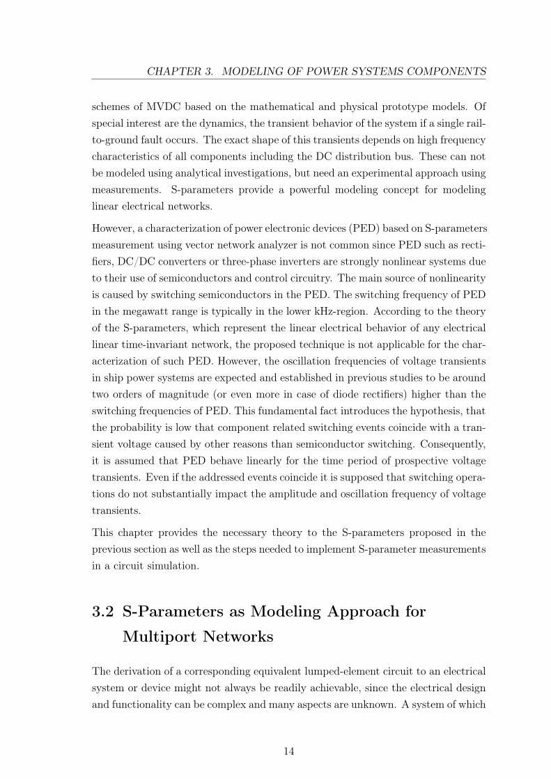
A multiport network as shown in Figure 3.1, often termed as N-port, is an arbitraryelectrical network which theoretically may have any number N of ports. A networkport is understood as a pair of terminals and can be explained as the point atwhich an electrical signal either enters or exits the network. Whereas impedanceand admittance matrices attempt to describe the relation between the total voltagesand currents of a network, existing at all ports present, the scattering matrix (S-Matrix) describes the transmission and reflection characteristics of the network interms of incident and reflected waves at all ports present [20, p.50]. In other words,total voltages and currents are considered to be in the form of travelling waves.
15
CHAPTER 3. MODELING OF POWER SYSTEMS COMPONENTS
1
⋮
Vs ZsV1
3
t1I1+-
N-1
2
4
N
ZLZL
ZLZL
ZLN-port
Network
⋮
a1b1 b2
b4bN
b3bN-1
t2
Figure 3.1: Arbitrary N-port network with ai and bi as the incident and reflectedwaves. Vs and Zs are the source voltage and source impedance. ZL isthe port termination equal to the source impedance. Vi is the potentialdifference between the ith-port and a reference (e.g. GND). Ii is thecurrent flow through the interface of port i and the load or source. Thereference planes are denoted as tx.
In literature, wave variables have been introduced and proposed by numerous au-thors in different ways due to several reasons such as convenience and physicalinterpretation purposes. Thus, the S-parameters are not uniquely defined which iswhy these differ in their meaning. In [21, p.27] a couple of these definitions arecovered more detailed. In [22] a new concept of traveling waves has been introducedwith respect to power why these are referred to as power waves. This definition ismost commonly applied and used here because it is suitable for this work as well.
A linear multiport in frequency domain is generally described in [23] by its S-parameters, utilizing the theory of linear superposition, in the following way
b1 = s11 a1 + s12 a2 + . . .+ s1N aN
b2 = s12 a1 + s22 a2 + . . .+ s2N aN (3.1)... =
...
bN = sN1 a1 + sN2 a2 + . . .+ sNN aN
16
CHAPTER 3. MODELING OF POWER SYSTEMS COMPONENTS
and can be reduced to a single equation using the matrix representation
b = Sa (3.2)
with a and b being the waves traveling towards (incident) the network and away(reflected) from the network at all ports present, and S denoting the S-matrix. Thusboth, a and b are vectors of dimension N×1 whereas S is a N×N matrix containingN2 elements, where N is the total number of ports. Considering a single port of a N-port network, generally denoted as the ith-port, a and b referring to [22] are definedin terms of the total voltage and current as
ai =Vi + ZiIi
2√|ReZi|
(3.3)
bi =Vi − Z∗i Ii2√|ReZi|
(3.4)
and called power waves, where Vi and Ii are the terminal voltage across and terminalcurrent through the ith-port and Zi is the complex reference impedance as seen fromthe ith-port or in other words, the impedance connected to the corresponding port.Physically treated, ai and bi are normalized incident and reflected peak voltagesand closely related with power. Accordingly |ai|2 and |bi|2 represent the powertraveling toward and back the ith-port of the network. To avoid any possibility ofmisunderstandings as to existing literature, in available textbooks and publications(e.g. [24][19][25]) same waves are denoted as incident and reflected wave amplitudes,as well as normalized or generalized power waves.
All the elements of the S-matrix (referred to as S-parameters)
S =
s11 . . . s1N... . . . ...sN1 . . . sNN
(3.5)
are a function of frequency as well of the locations of the reference or terminal planestx (define the network ports) and defined for steady-state stimuli in terms of a setof N reference impedances. Consequently, S becomes a matrix N × N ×M , repre-senting M N-port S-parameters, where M is the total number of frequency points.The expressions (3.3) and (3.4) are defined for the use of any arbitrary character-istic impedance, for the simple reason that under general conditions the referenceimpedances are not required to be purely resistive and different impedances Zi can
17
CHAPTER 3. MODELING OF POWER SYSTEMS COMPONENTS
be used at each port, even complex. In conjunction with this, the notion gener-alized power wave is used. S-parameters are most commonly given with referenceto a 50 Ω test environment, meaning that Zi is a real-valued positive impedance,typically denoted as Z0 and identical at all ports present. In this case the previouslydefined power waves are equal with the expressions with those known in literatureas traveling waves [22].
Considering S-parameters, each element of the main diagonal of S is a reflectioncoefficient of a corresponding port when the other ports are terminated by perfectmatched loads [26, p.90] and contains the ratio of amplitude of reflected and incidentwave of a certain frequency. Conversely, the off-diagonal elements are transmissioncoefficients between the ports containing the ratio of amplitude of transmitted andincident wave. The related requirements prior are applicable as well. Following this,S-parameter of the main diagonal can be determined as
sii =biai
∣∣∣∣ak=0∀ k 6=i
(3.6)
with bi being the reflected power wave amplitude and ai being the incident powerwave amplitude at the ith-port. The off-diagonal S-parameters can be found as
sij =biai
∣∣∣∣ak=0∀ k 6=j
(3.7)
with bi being the transmitted power wave amplitude and and aj being the incidentpower wave amplitude at the jth-port. The subscripted condition implies that nopower waves are returned to the network from all other ports k which are considerednot being stimulated but to be connected to perfect matched loads. Following the S-parameter convention sij, the first subscript (i) always refers to the responding portor in other words to the port at which the wave is travelling outward the network.The second subscript (j) refers to the port to which the wave is travelling towards.Assuming, power is fed into an arbitrary multiport network over the junction of port1 and the signal is exiting the network at port 4, the determined S-parameter is thetransmission coefficient s41.
The S-parameters are depending on the accuracy of the reference impedances (sourceand load) used for the measurement as well as on the frequency those are measuredat and of course on the network itself including the plane of reference which definesthe position where the measurements are made. Observing the characteristics of
18
CHAPTER 3. MODELING OF POWER SYSTEMS COMPONENTS
the travelling waves, the transmitted and reflected waves will be changed by thenetwork in amplitude and phase in comparison to the incident wave, whereas thefrequency remains unaffected and stays the same. Due to that fact, S-parametersare expressed as complex numbers representing magnitude and phase angle at eachpoint of frequency. Whereas such a representation is very convenient for post-processing operations, for interpretation purposes these parameters often posed inlinear form as amplitude and phase or in case of logarithmic scale with magnitudein decibels (Bode plot). In microwave theory S-parameters are often displayed on aso-called “Smith Chart” [27]. For the sake of completeness, [28] contains tables howS-parameters can be converted to and from alternative network parameters.
3.3 Measurement of Scattering Parameters of an
N-port Network
3.3.1 Vector Network Analyzer
Today various simulation software packages (e.g. MATLAB or Agilent AdvancedDesign Software (ADS)1) routinely used in the high-frequency engineering as well asfinite element analysis software packages such as Comsol Multiphysics2 permit theextraction and manipulation of network parameters such as Y, Z, and S-parametersof electrical networks in a relatively simple process. If used to characterize a circuit,they are typically measured based on experiments by the use of vector networkanalyzers (VNAs).
The capability to provide error corrected amplitude and phase characterization ofactive and passive components makes the VNA to a powerful and flexible mea-suring instrument and thus to one of the standard test tools for RF and microwaveengineers. A VNA typically measures the S-parameters because reflection and trans-mission of electrical networks can be measured accurately even at high frequencies.To determine the S-parameters of components, circuits, cables or antennas, the VNAsweeps a sinusoidal electrical signal linearly or logarithmically through a user spec-ified frequency range and measures the magnitude and phase characteristics. Themeasurement of both, magnitude and phase is necessary for a complete characteriza-tion of the device under test (DUT). Even though the magnitude only data might be
1http://www.home.agilent.com/en/pc-1297113/advanced-design-system-ads2http://www.comsol.com/
19
CHAPTER 3. MODELING OF POWER SYSTEMS COMPONENTS
fully sufficient in many situations (e.g. gain of an amplifier), for the development ofcircuit models for simulations the phase information is needed as well. Furthermore,the phase data is used by the VNA itself to perform vector error correction.
As the DUT features a unique performance at a certain frequency from one portto another, the S-parameters are preferably determined within a certain frequencyrange of interest with a high density of frequency points, typically hundreds orsometimes exceeding one thousand. The frequency range can start as low as inthe range of a few hertz and stop as high as in the gigahertz range. A completesweep is usually just a matter of a few seconds or less and measures directly thecorresponding S-Matrix at each frequency point.
Although multiport vector network analyzers have become more popular in the re-cent years and commercially available, two-port VNAs are most common since thoseare more reasonable in price. Two-port network analyzers are often used to charac-terize two-port networks such as amplifiers and filters. Modern VNAs allow export-ing the set of S-parameters in the unified industry-standard format “Touchstone”,specified in [29] which can be imported easily by computing software packages suchas MATLAB (with “RF Toolbox”). The specification gives a clear instruction howa set of S-parameters must be stored in the output file in order to facilitate an easyreadout. The comprehensive and convenient measurement procedure supports theproposed approach.
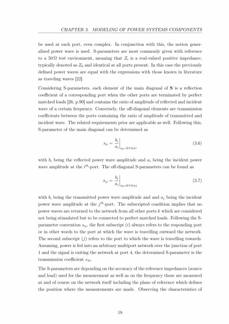
In this work a 2-port network analyzer from Agilent has been used (Figure 3.2).Beside a full 2-port calibration it provides S-parameter measurements from 30 kHz
to 6 GHz by 1601 frequency points in total. This VNA does not support the outputof Touchstone files (*.s2p). Therefore, additional steps are required to obtain thedesired output file. This concern is discussed in Appendix B - B.4.
Figure 3.2: 2-port vector network analyzer (VNA) Agilent 8753ES available at theNational High Magnetic Field Laboratory (NHMFL) [30]
20
CHAPTER 3. MODELING OF POWER SYSTEMS COMPONENTS
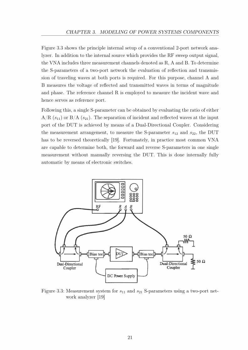
Figure 3.3 shows the principle internal setup of a conventional 2-port network ana-lyzer. In addition to the internal source which provides the RF sweep output signal,the VNA includes three measurement channels denoted as R, A and B. To determinethe S-parameters of a two-port network the evaluation of reflection and transmis-sion of traveling waves at both ports is required. For this purpose, channel A andB measures the voltage of reflected and transmitted waves in terms of magnitudeand phase. The reference channel R is employed to measure the incident wave andhence serves as reference port.
Following this, a single S-parameter can be obtained by evaluating the ratio of eitherA/R (s11) or B/A (s21). The separation of incident and reflected waves at the inputport of the DUT is achieved by means of a Dual-Directional Coupler. Consideringthe measurement arrangement, to measure the S-parameter s12 and s22, the DUThas to be reversed theoretically [19]. Fortunately, in practice most common VNAare capable to determine both, the forward and reverse S-parameters in one singlemeasurement without manually reversing the DUT. This is done internally fullyautomatic by means of electronic switches.
Figure 3.3: Measurement system for s11 and s21 S-parameters using a two-port net-work analyzer [19]
21
CHAPTER 3. MODELING OF POWER SYSTEMS COMPONENTS
3.3.2 Multiport Measurement by Means of a Two-Port
Vector Network Analyzer
Common components of a 3-phase power system such as rotating machines, powerelectronics (DC/DC converter, DC/AC inverter) or cabling are multiport networks.This encounters the question how to characterize a multiport network (N > 2) usinga Two-Port VNA. Referring to [31] several partial two-ports measurements must beperformed with the Two-Port VNA connected to various combinations of the N-port network while terminating all other remaining (N− 2)-ports of the DUT withperfectly matched loads (system impedance, e.g. 50 Ω) to follow the definition ofS-parameters. The number of required measurements can be found by(
N2
)=
N(N− 1)
2(3.8)
where N is the number of ports. Note, equation 3.8 implies, that forward and reverseS-parameters of the DUT are determined in one single measurement. In case of anupgrade to a newer one (e.g. 4-port VNA), it might be important to know, that foran M-port VNA where M is even and N is a multiple of M
2, it is conjectured that
the required number of measurements is given by
N(2N−M)
M2 (3.9)
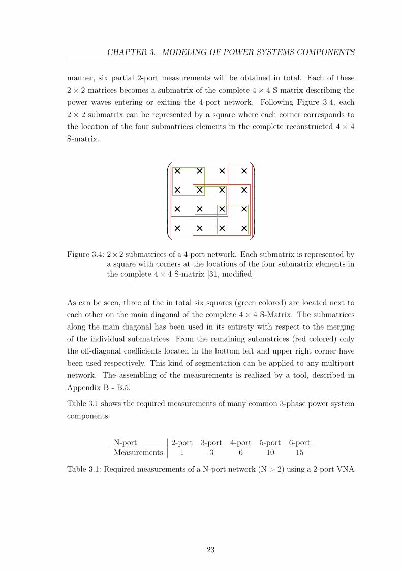
As shown in Figure 3.5, for a 4-port network (e.g. DC/DC Converter, DC bus)for example six two-port measurements need to be conducted. For instance, in thefirst two-port measurements the VNA port 1 is connected to port 1 of the DUTand VNA port 2 connected to port 2 of the DUT. The remaining ports 3 and 4 ofthe DUT terminated by a 50 Ω load. Then, the measurement result yields a 2 × 2
partial S-matrix of the DUT containing the S-parameters s11, s12, s21 and s22. In thesecond two-port measurement, VNA port 1 is connected to DUT port 1 and VNAport 2 connected to DUT port 3. The remaining ports 2 and 4 of the DUT are againterminated by a 50 Ω load. The measurement result yields again a 2 × 2 partial S-Matrix of the DUT containing the same S-Parameters as before, but those are nowequivalent to s11, s13, s31 and s33 respectively. Furthermore, it can be seen thatdiagonal S-parameters are measured multiple times. Generally, N − 1 independentmeasurements of the reflection coefficient sii at each of the four ports are made.
Continuing this process with the remaining two-port measurements in the same
22
CHAPTER 3. MODELING OF POWER SYSTEMS COMPONENTS
manner, six partial 2-port measurements will be obtained in total. Each of these2 × 2 matrices becomes a submatrix of the complete 4 × 4 S-matrix describing thepower waves entering or exiting the 4-port network. Following Figure 3.4, each2 × 2 submatrix can be represented by a square where each corner corresponds tothe location of the four submatrices elements in the complete reconstructed 4 × 4
S-matrix.
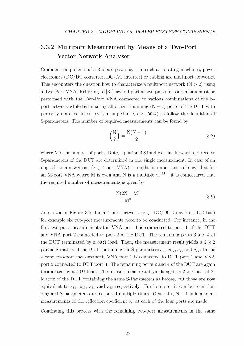
× × × ×
× × × × × × × × × × × ×
Figure 3.4: 2×2 submatrices of a 4-port network. Each submatrix is represented bya square with corners at the locations of the four submatrix elements inthe complete 4× 4 S-matrix [31, modified]
As can be seen, three of the in total six squares (green colored) are located next toeach other on the main diagonal of the complete 4 × 4 S-Matrix. The submatricesalong the main diagonal has been used in its entirety with respect to the mergingof the individual submatrices. From the remaining submatrices (red colored) onlythe off-diagonal coefficients located in the bottom left and upper right corner havebeen used respectively. This kind of segmentation can be applied to any multiportnetwork. The assembling of the measurements is realized by a tool, described inAppendix B - B.5.
Table 3.1 shows the required measurements of many common 3-phase power systemcomponents.
N-port 2-port 3-port 4-port 5-port 6-portMeasurements 1 3 6 10 15
Table 3.1: Required measurements of a N-port network (N > 2) using a 2-port VNA
23
CHAPTER 3. MODELING OF POWER SYSTEMS COMPONENTS
(1)
(2)
(3)
(4)
(1)
(2)
(3)
(4)
(1)
(2)
(3)
(4)
(1)
(2)
(3)
(4)
(1)
(2)
(3)
(4)
(1)
(2)
(3)
(4)
… 50Ω Terminator
s s
s s
33 3443 44
s s
s s
22 2442 44
s s
s s
22 2332 33
s s
s s
11 1441 44
s s
s s
11 1331 33
s s
s s
11 1221 22
Figure 3.5: Different measurement combinations of a 4-port Network using a 2-portVNA. The matrices contain the corresponding S-parameters obtained byeach measurement respectively.
3.3.3 Measurement of Purdue’s Small Scale Testbed
Components
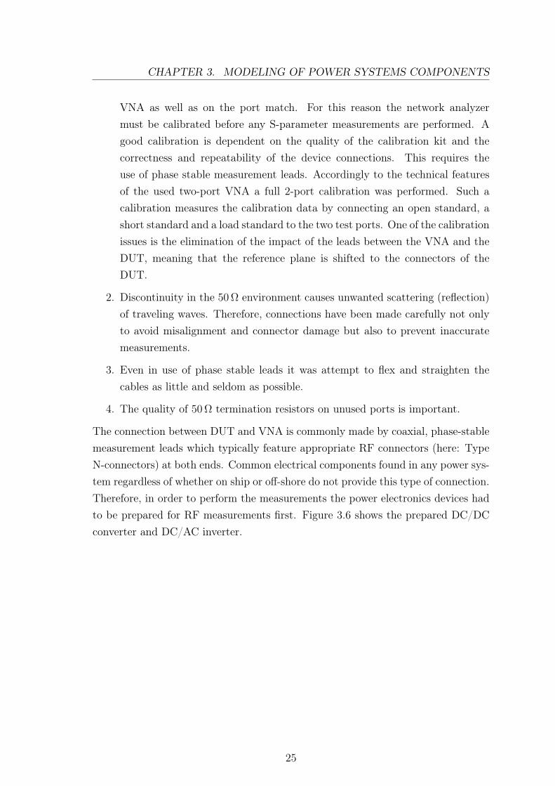
Students under the supervision of Prof. Steve Pekarek at Purdue University built anexperimental small-scale testbed of a simplified shipboard power system for ground-ing studies. This testbed has strong architectural similarities to power systems beinginvestigated for future naval ships. The power electronics include an American PowerDesign DC/DC converter with a switching frequency of 85 kHz with a 100 V/100 W
output rating and a custom-designed 3-phase inverter with a switching frequency of100 kHz and variable frequency output. In this work both, the S-parameters of theDC/DC converter and the 3-phase inverter have been measured.
For the measurement a typical setup including the VNA, a calibration kit as well asa set of cables and loads has been used. All components featuring an impedance of50 Ω. To obtain measurements with highest possible accuracy, the following stepshave been considered and observed:
1. The accuracy of the measurement strongly depends on the accuracy of the
24
CHAPTER 3. MODELING OF POWER SYSTEMS COMPONENTS
VNA as well as on the port match. For this reason the network analyzermust be calibrated before any S-parameter measurements are performed. Agood calibration is dependent on the quality of the calibration kit and thecorrectness and repeatability of the device connections. This requires theuse of phase stable measurement leads. Accordingly to the technical featuresof the used two-port VNA a full 2-port calibration was performed. Such acalibration measures the calibration data by connecting an open standard, ashort standard and a load standard to the two test ports. One of the calibrationissues is the elimination of the impact of the leads between the VNA and theDUT, meaning that the reference plane is shifted to the connectors of theDUT.
2. Discontinuity in the 50 Ω environment causes unwanted scattering (reflection)of traveling waves. Therefore, connections have been made carefully not onlyto avoid misalignment and connector damage but also to prevent inaccuratemeasurements.
3. Even in use of phase stable leads it was attempt to flex and straighten thecables as little and seldom as possible.
4. The quality of 50 Ω termination resistors on unused ports is important.
The connection between DUT and VNA is commonly made by coaxial, phase-stablemeasurement leads which typically feature appropriate RF connectors (here: TypeN-connectors) at both ends. Common electrical components found in any power sys-tem regardless of whether on ship or off-shore do not provide this type of connection.Therefore, in order to perform the measurements the power electronics devices hadto be prepared for RF measurements first. Figure 3.6 shows the prepared DC/DCconverter and DC/AC inverter.
25
CHAPTER 3. MODELING OF POWER SYSTEMS COMPONENTS
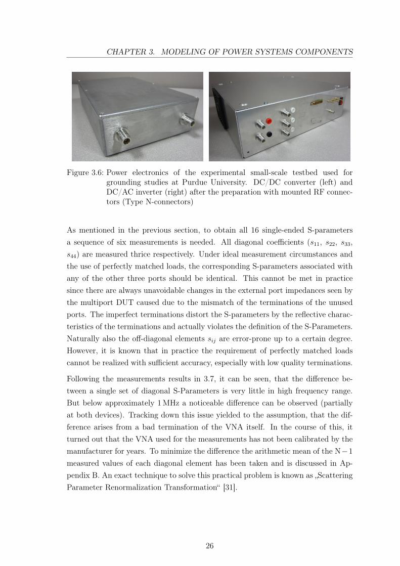
Figure 3.6: Power electronics of the experimental small-scale testbed used forgrounding studies at Purdue University. DC/DC converter (left) andDC/AC inverter (right) after the preparation with mounted RF connec-tors (Type N-connectors)
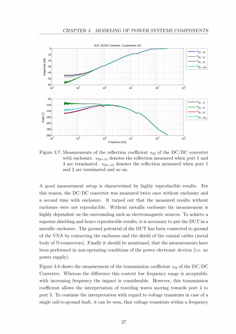
As mentioned in the previous section, to obtain all 16 single-ended S-parametersa sequence of six measurements is needed. All diagonal coefficients (s11, s22, s33,s44) are measured thrice respectively. Under ideal measurement circumstances andthe use of perfectly matched loads, the corresponding S-parameters associated withany of the other three ports should be identical. This cannot be met in practicesince there are always unavoidable changes in the external port impedances seen bythe multiport DUT caused due to the mismatch of the terminations of the unusedports. The imperfect terminations distort the S-parameters by the reflective charac-teristics of the terminations and actually violates the definition of the S-Parameters.Naturally also the off-diagonal elements sij are error-prone up to a certain degree.However, it is known that in practice the requirement of perfectly matched loadscannot be realized with sufficient accuracy, especially with low quality terminations.
Following the measurements results in 3.7, it can be seen, that the difference be-tween a single set of diagonal S-Parameters is very little in high frequency range.But below approximately 1 MHz a noticeable difference can be observed (partiallyat both devices). Tracking down this issue yielded to the assumption, that the dif-ference arises from a bad termination of the VNA itself. In the course of this, itturned out that the VNA used for the measurements has not been calibrated by themanufacturer for years. To minimize the difference the arithmetic mean of the N−1
measured values of each diagonal element has been taken and is discussed in Ap-pendix B. An exact technique to solve this practical problem is known as „ScatteringParameter Renormalization Transformation“ [31].
26
CHAPTER 3. MODELING OF POWER SYSTEMS COMPONENTS
104
105
106
107
108
109
-60
-50
-40
-30
-20
-10
0DUT: DC/DC Converter, S-parameter s33
Mag
nitu
de [
dB]
104
105
106
107
108
109
-350
-300
-250
-200
-150
-100
-50
Frequency [Hz]
Ang
le [
°]
s33←14
s33←12
s33←24
s33←avg
s33←14
s33←12
s33←24
s33←avg
Figure 3.7: Measurements of the reflection coefficient s33 of the DC/DC converterwith enclosure. s33←14 denotes the reflection measured when port 1 and4 are terminated. s33←12 denotes the reflection measured when port 1and 2 are terminated and so on.
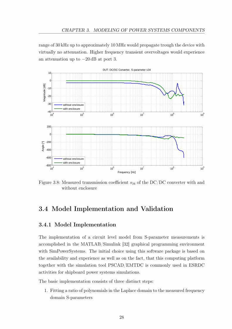
A good measurement setup is characterized by highly reproducible results. Forthis reason, the DC/DC converter was measured twice once without enclosure anda second time with enclosure. It turned out that the measured results withoutenclosure were not reproducible. Without metallic enclosure the measurement ishighly dependent on the surrounding such as electromagnetic sources. To achieve asuperior shielding and hence reproducible results, it is necessary to put the DUT in ametallic enclosure. The ground potential of the DUT has been connected to groundof the VNA by contacting the enclosure and the shield of the coaxial cables (metalbody of N-connectors). Finally it should be mentioned, that the measurements havebeen performed in non-operating conditions of the power electronic devices (i.e. nopower supply).
Figure 3.8 shows the measurement of the transmission coefficient s34 of the DC/DCConverter. Whereas the difference this context low frequency range is acceptable,with increasing frequency the impact is considerable. However, this transmissioncoefficient allows the interpretation of traveling waves moving towards port 4 toport 3. To continue the interpretation with regard to voltage transients in case of asingle rail-to-ground fault, it can be seen, that voltage transients within a frequency
27
CHAPTER 3. MODELING OF POWER SYSTEMS COMPONENTS
range of 30 kHz up to approximately 10 MHz would propagate trough the device withvirtually no attenuation. Higher frequency transient overvoltages would experiencean attenuation up to −20 dB at port 3.
104
105
106
107
108
109
-40
-30
-20
-10
0
10DUT: DC/DC Converter, S-parameter s34
Mag
nitu
de [
dB]
104
105
106
107
108
109
-800
-600
-400
-200
0
200
Frequency [Hz]
Ang
le [
°]
without enclosure
with enclosure
without enclosure
with enclosure
Figure 3.8: Measured transmission coefficient s34 of the DC/DC converter with andwithout enclosure
3.4 Model Implementation and Validation
3.4.1 Model Implementation
The implementation of a circuit level model from S-parameter measurements isaccomplished in the MATLAB/Simulink [32] graphical programming environmentwith SimPowerSystems. The initial choice using this software package is based onthe availability and experience as well as on the fact, that this computing platformtogether with the simulation tool PSCAD/EMTDC is commonly used in ESRDCactivities for shipboard power systems simulations.
The basic implementation consists of three distinct steps:
1. Fitting a ratio of polynomials in the Laplace domain to the measured frequencydomain S-parameters
28
CHAPTER 3. MODELING OF POWER SYSTEMS COMPONENTS
2. Building transfer function blocks for each S-parameter
3. Incorporating these blocks into a circuit level model
3.4.1.1 Rational Function Modeling and Fitting
In the previous chapter it has been described how to obtain S-parameters of anN-port network. The result is a rather extensive set of data of measured frequencydomain data, representing the S-parameters. In order to use these data for simula-tion purpose, the frequency domain measurement data have to be fitted in frequncydomain model descriptions such as transfer functions for the S-parameters. Note, inthe previous chapter the lowercase “s” is used for S-parameters which might confusesince in the Laplace domain the same character represents the complex frequency.For this reason in this section S-parameters are indicated with an uppercase “S”.
The objective of the fitting procedure (“rational fit”) is to create a mathematicalmodel from the complex frequency domain data. Conceptually, this model wouldbe a ratio of polynomials in the Laplace variable s. For instance, the finite set ofmeasurement data can be approximated by:
S12(s) =aNs
N + aN−1sN−1 + . . .+ a1s+ a0
bMsM + bM−1sM−1 + . . .+ b1s+ b0(3.10)
where s = σ + jω is the complex frequency with ω = 2πf .
The polynomials involved with this approximation are typically of a high order (e.g.M > 30) and high frequencies are involved as well. For instance, when modelinghigh speed serial data physical interconnects, the upper bounds of frequency areoften well over 10 GHz. This creates a serious numerical challenge for the aboveformulation. The solution is to reformulate the problem into a more numericallyfriendly canonic form, a partial fraction expansion:
S12(s) =M∑m=1
cms− pm
+ d (3.11)
where pm are pole locations, cm are the residues to the corresponding poles and d isthe direct feedthrough term which appears if the lengths of the numerator coefficientsand denomiator coefficients are equal (M = N).
This approximation works well for lumped element systems which naturally havea finite order. But in our case, the measurements have been made on distributed
29
CHAPTER 3. MODELING OF POWER SYSTEMS COMPONENTS
systems which in principle, have an infinite order. The distributed nature is due tothe measurements being made on physically large elements that behave like trans-mission lines. One manifestation of this behavior is a time delay for end-to-endoff-diagonal measurements such as S12 and S21. A small modification can be madeto the partial fraction expansion to include the time delay:
S12(s) =
(M∑m=1
cms− pm
+ d
)e−sτ (3.12)
where τ is a coarse estimate of the time delay.
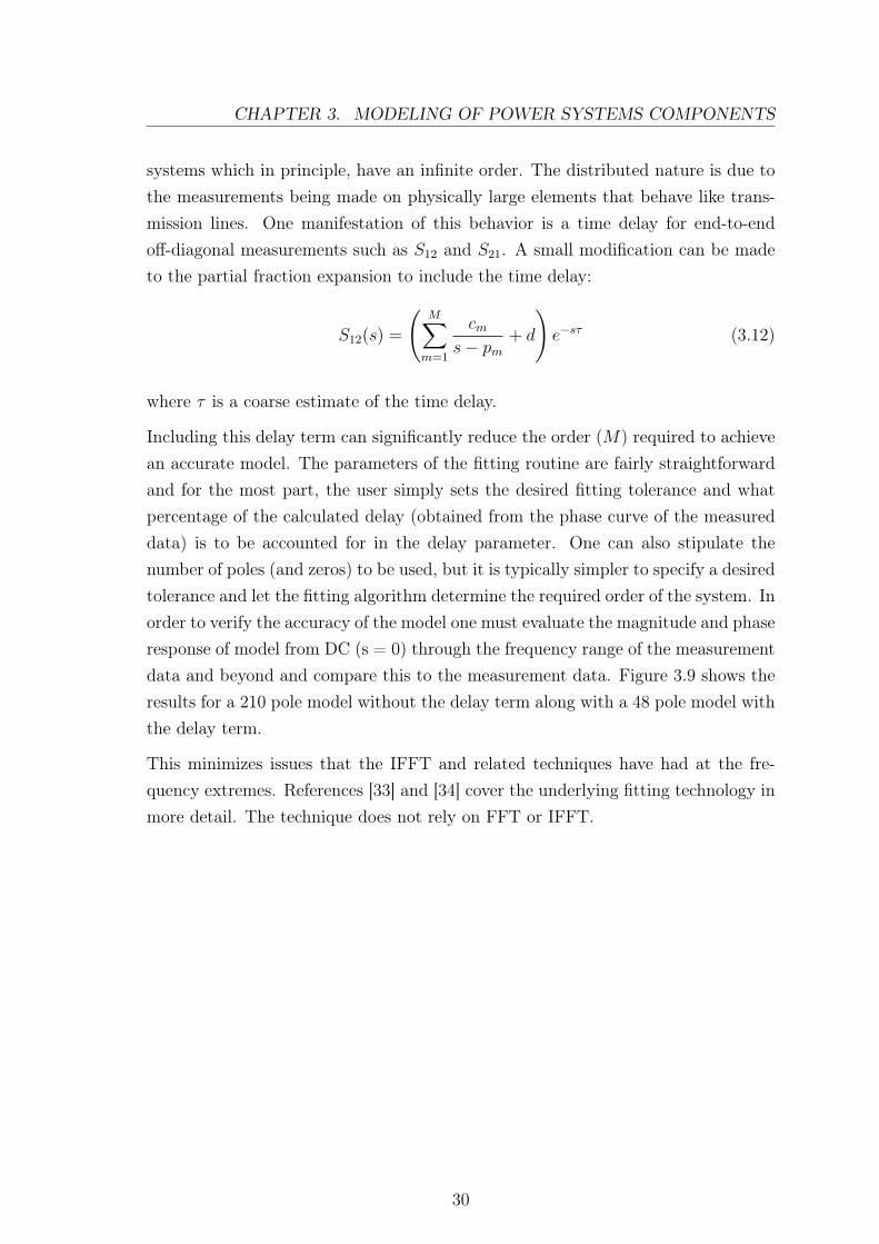
Including this delay term can significantly reduce the order (M) required to achievean accurate model. The parameters of the fitting routine are fairly straightforwardand for the most part, the user simply sets the desired fitting tolerance and whatpercentage of the calculated delay (obtained from the phase curve of the measureddata) is to be accounted for in the delay parameter. One can also stipulate thenumber of poles (and zeros) to be used, but it is typically simpler to specify a desiredtolerance and let the fitting algorithm determine the required order of the system. Inorder to verify the accuracy of the model one must evaluate the magnitude and phaseresponse of model from DC (s = 0) through the frequency range of the measurementdata and beyond and compare this to the measurement data. Figure 3.9 shows theresults for a 210 pole model without the delay term along with a 48 pole model withthe delay term.
This minimizes issues that the IFFT and related techniques have had at the fre-quency extremes. References [33] and [34] cover the underlying fitting technology inmore detail. The technique does not rely on FFT or IFFT.
30
CHAPTER 3. MODELING OF POWER SYSTEMS COMPONENTS
Figure 3.9: Comparison between the frequency response of the rational function ob-ject and that of the original data [34]
3.4.1.2 Generation of Transfer Function Blocks
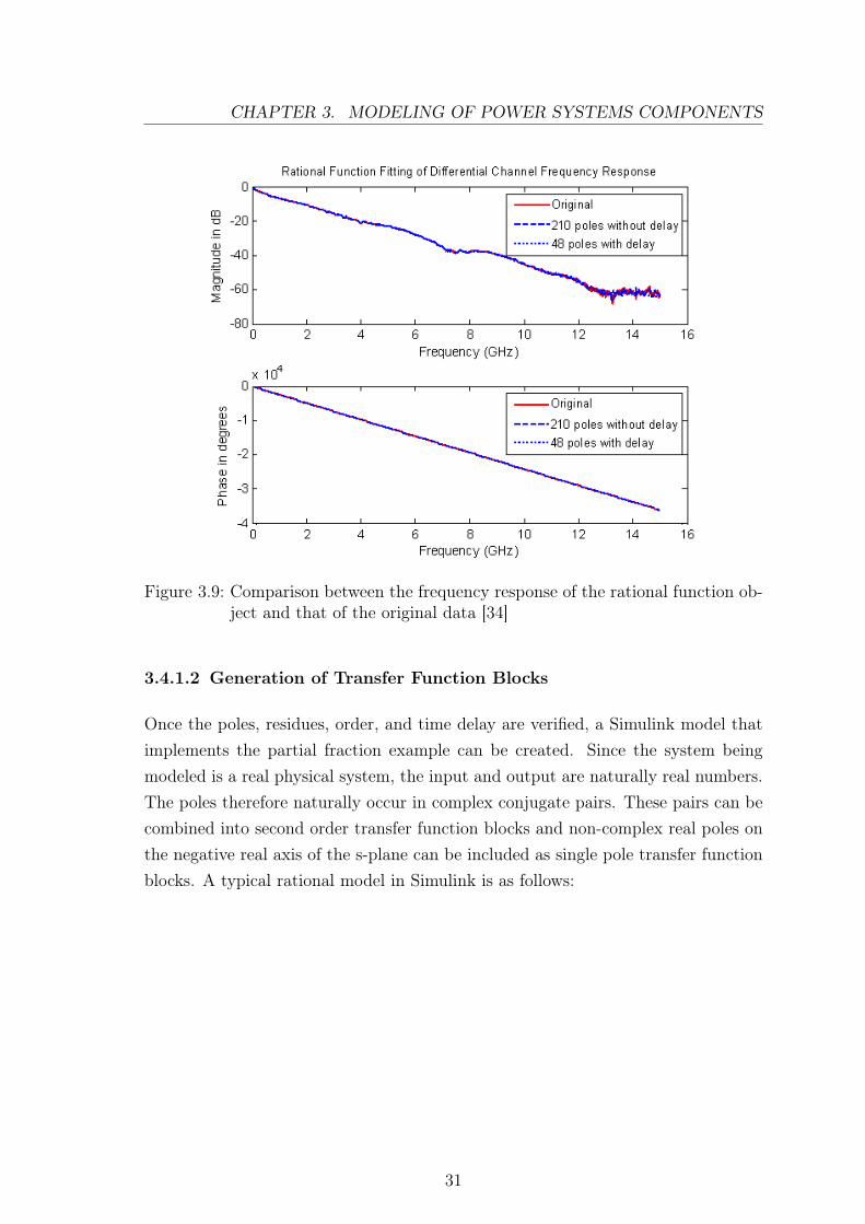
Once the poles, residues, order, and time delay are verified, a Simulink model thatimplements the partial fraction example can be created. Since the system beingmodeled is a real physical system, the input and output are naturally real numbers.The poles therefore naturally occur in complex conjugate pairs. These pairs can becombined into second order transfer function blocks and non-complex real poles onthe negative real axis of the s-plane can be included as single pole transfer functionblocks. A typical rational model in Simulink is as follows:
31
CHAPTER 3. MODELING OF POWER SYSTEMS COMPONENTS
1
Out1
num(s)
den(s)
stage_6
den(s)
num(s)
stage_5
num(s)
den(s)
stage_4
num(s)
den(s)
stage_3
num(s)
den(s)
stage_2
num(s)
den(s)
stage_1
-K-
Direct FeedthroughDelay
Combiner
Add
1
In1
Figure 3.10: Simulink model for a rational function representing a single S-parameter
The transfer function blocks (“stages” in Figure 3.10) are of second and first or-der. They implement the complex conjugate pole pairs, and real poles and thecorresponding residues respectively. Note, each transfer function block always hasreal coefficients. This is why the poles and corresponding residues of the rationalfunction object of each S-parameter needs to be converted into real numerators anddenominators for use in the Laplace Transform transfer function blocks. This isaccomplished by equation 3.13 and 3.14.
F (s) =cm
s− pm(3.13)
F (s) =2Re cm s− 2 (Re cmRe pm+ Im cm Im pm)
s2 − 2Re pm s+ Re pm2 + Im pm2(3.14)
Figure 3.10 shows a relatively low order model as compared to what real-worldmeasurement data requires. But even this low order model would be very tedious anderror prone to create manually. Fortunately MATLAB can programmatically builda Simulink model with some relatively simple commands making the constructionof far more complex (higher order) models effortless.
32
CHAPTER 3. MODELING OF POWER SYSTEMS COMPONENTS
3.4.1.3 Circuit Level Model Implementation
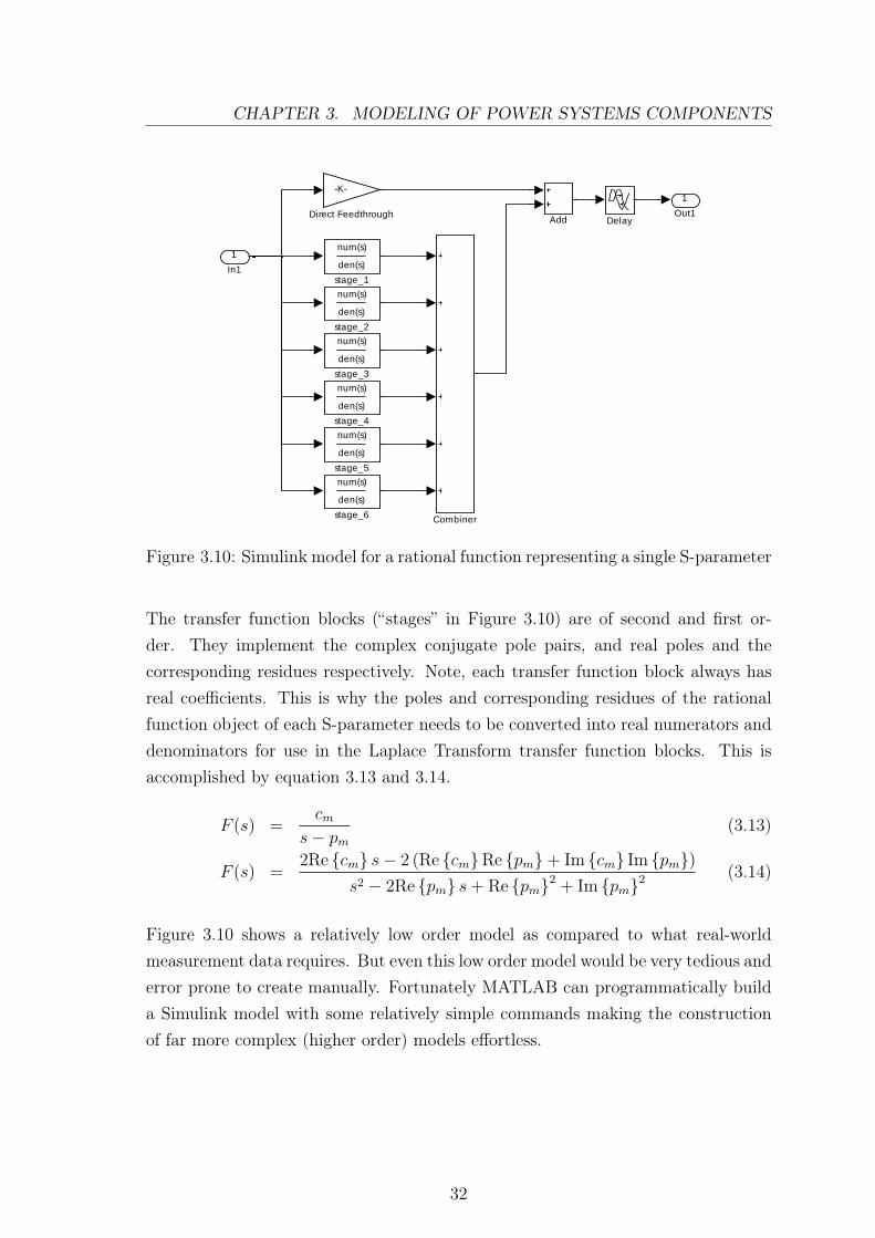
The discussion is continued on a 2-port example, but the proposed approach canbe easily extended to N ports, which allows to study many of the most commoncomponents of a 3-phase power system (e.g. N = 6). The final step in the modelingprocess is to include the 4 rational transfer function blocks in a circuit level environ-ment. Table 3.2 shows the number of transfer function blocks needed to implementa N-port network. SimPowerSystems, a toolbox for Simulink, allows to model powersystems in a similar fashion as SPICE3. Unlike SPICE, it is optimized for the needsof a power systems engineer. However, the stock tool does not have the ability tomodel from S-parameters, but it can be extended to do so by using controlled sourcesand measurements of both voltage and current. From a “top level”, the S-parametermodel looks as shown in Figure 3.11.
N-port 2-port 3-port 4-port 5-port 6-portMeasurements 4 9 16 25 36
Table 3.2: Number of rational transfer function blocks needed to implement a N-portnetwork into a circuit simulation
Vin
Continuous
powergui
+
Zs
+
Zl
s -+
Vin
v+-
VMS
v+-
VML
Step
Scope
S-parameters Block
S-parameters
Vout
Figure 3.11: S-parameter model block build in Simulink/SimPowerSystems. Arbi-trary complex passive and active sources and loads can be incorporatedaround the S-parameters model block
The interface between the unidirectional signal domain of Simulink and the circuitdomain of SimPowerSystems is accomplished with the “Vin” block (a controlled
3Simulation Program with Integrated Circuit Emphasis [35]
33
CHAPTER 3. MODELING OF POWER SYSTEMS COMPONENTS
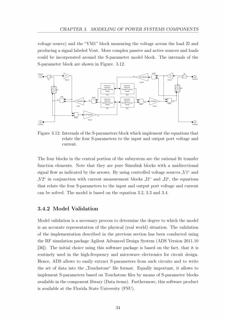
voltage source) and the “VM1” block measuring the voltage across the load Zl andproducing a signal labeled Vout. More complex passive and active sources and loadscould be incorporated around the S-parameter model block. The internals of theS-parameter block are shown in Figure. 3.12.
4
Conn4
3
Conn2
2
Conn3
1
Conn1
s -+
V2
s -+
V1
S-Domain Rational
Transfer Function Model
S22
S-Domain Rational
Transfer Function Model
S21
S-Domain Rational
Transfer Function Model
S12
S-Domain Rational
Transfer Function Model
S11
i+
-
I2
i+
-
I1
1/(2*sqrt(Zo))
Gain5
2*sqrt(Zo)
Gain4
Zo
Gain3
1/(2*sqrt(Zo))
Gain2
Zo
Gain1
2*sqrt(Zo)
Gain
Add5
Add4 Add3
Add2
Add1
Add
a2
b2 V2b1V1
a1
Figure 3.12: Internals of the S-parameters block which implement the equations thatrelate the four S-parameters to the input and output port voltage andcurrent.
The four blocks in the central portion of the subsystem are the rational fit transferfunction elements. Note that they are pure Simulink blocks with a unidirectionalsignal flow as indicated by the arrows. By using controlled voltage sources „V1“ and„V2“ in conjunction with current measurement blocks „I1“ and „I2“, the equationsthat relate the four S-parameters to the input and output port voltage and currentcan be solved. The model is based on the equation 3.2, 3.3 and 3.4.
3.4.2 Model Validation
Model validation is a necessary process to determine the degree to which the modelis an accurate representation of the physical (real world) situation. The validationof the implementation described in the previous section has been conducted usingthe RF simulation package Agilent Advanced Design System (ADS Version 2011.10[36]). The initial choice using this software package is based on the fact, that it isroutinely used in the high-frequency and microwave electronics for circuit design.Hence, ADS allows to easily extract S-parameters from such circuits and to writethe set of data into the „Touchstone“ file format. Equally important, it allows toimplement S-parameters based on Touchstone files by means of S-parameter blocksavailable in the component library (Data items). Furthermore, this software productis available at the Florida State University (FSU).
34
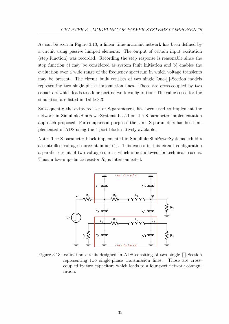
CHAPTER 3. MODELING OF POWER SYSTEMS COMPONENTS
As can be seen in Figure 3.13, a linear time-invariant network has been defined bya circuit using passive lumped elements. The output of certain input excitation(step function) was recorded. Recording the step response is reasonable since thestep function a) may be considered as system fault initiation and b) enables theevaluation over a wide range of the frequency spectrum in which voltage transientsmay be present. The circuit built consists of two single One-
∏-Section models
representing two single-phase transmission lines. Those are cross-coupled by twocapacitors which leads to a four-port network configuration. The values used for thesimulation are listed in Table 3.3.
Subsequently the extracted set of S-parameters, has been used to implement thenetwork in Simulink/SimPowerSystems based on the S-parameter implementationapproach proposed. For comparison purposes the same S-parameters has been im-plemented in ADS using the 4-port block natively available.
Note: The S-parameter block implemented in Simulink/SimPowerSystems exhibitsa controlled voltage source at input (1). This causes in this circuit configurationa parallel circuit of two voltage sources which is not allowed for technical reasons.Thus, a low-impedance resistor R1 is interconnected.
Figure 3.13: Validation circuit designed in ADS consiting of two single∏-Section
representing two single-phase transmission lines. Those are cross-coupled by two capacitors which leads to a four-port network configu-ration.
35
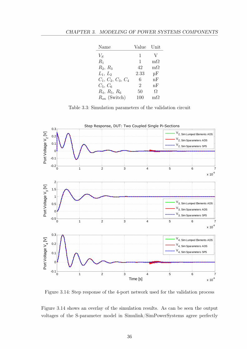
CHAPTER 3. MODELING OF POWER SYSTEMS COMPONENTS
Name Value Unit
VS 1 VR1 1 mΩR2, R3 42 mΩL1, L2 2.33 µFC1, C2, C3, C4 6 nFC5, C6 2 nFR4, R5, R6 50 ΩRon (Switch) 100 mΩ
Table 3.3: Simulation parameters of the validation circuit
0 1 2 3 4 5 6 7
x 10-6
-0.2
-0.1
0
0.1
0.2
0.3
Time [s]
Por
t Vol
tage
V2 [V
]
Step Response 4-port Network
V2, Sim Lumped Elements ADS
V2, Sim Sparameters ADS
V2, Sim Sparameters SPS
0 1 2 3 4 5 6 7
x 10-6
-0.5
0
0.5
1
1.5
2
Time [s]
Por
t Vol
tage
V3 [V
]
Step Response 4-port Network
V3, Sim Lumped Elements ADS
V3, Sim Sparameters ADS
V3, Sim Sparameters SPS
0 1 2 3 4 5 6 7
x 10-6
-0.1
0
0.1
0.2
0.3
Time [s]
Por
t Vol
tage
V4 [V
]
Step Response 4-port Network
V4, Sim Lumped Elements ADS
V4, Sim Sparameters ADS
V4, Sim Sparameters SPS
Step Response, DUT: Two Coupled Single Pi-Sections
Figure 3.14: Step response of the 4-port network used for the validation process
Figure 3.14 shows an overlay of the simulation results. As can be seen the outputvoltages of the S-parameter model in Simulink/SimPowerSystems agree perfectly
36
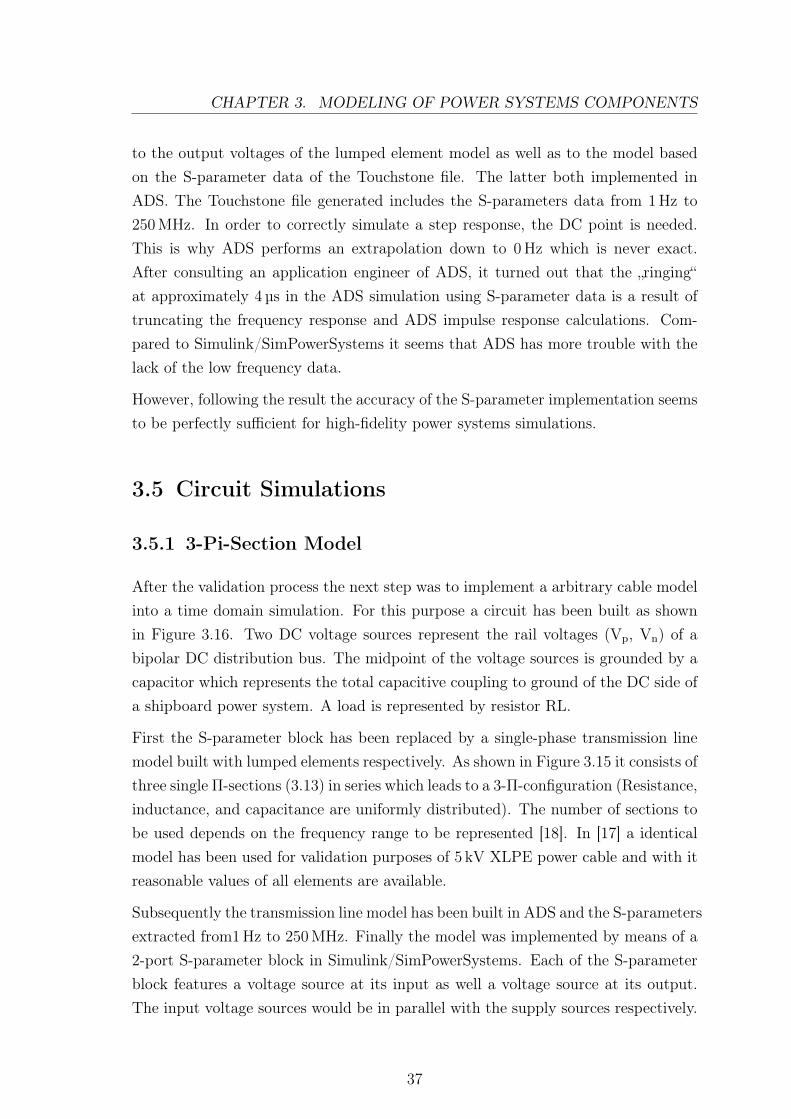
CHAPTER 3. MODELING OF POWER SYSTEMS COMPONENTS
to the output voltages of the lumped element model as well as to the model basedon the S-parameter data of the Touchstone file. The latter both implemented inADS. The Touchstone file generated includes the S-parameters data from 1 Hz to250 MHz. In order to correctly simulate a step response, the DC point is needed.This is why ADS performs an extrapolation down to 0 Hz which is never exact.After consulting an application engineer of ADS, it turned out that the „ringing“at approximately 4 µs in the ADS simulation using S-parameter data is a result oftruncating the frequency response and ADS impulse response calculations. Com-pared to Simulink/SimPowerSystems it seems that ADS has more trouble with thelack of the low frequency data.
However, following the result the accuracy of the S-parameter implementation seemsto be perfectly sufficient for high-fidelity power systems simulations.
3.5 Circuit Simulations
3.5.1 3-Pi-Section Model
After the validation process the next step was to implement a arbitrary cable modelinto a time domain simulation. For this purpose a circuit has been built as shownin Figure 3.16. Two DC voltage sources represent the rail voltages (Vp, Vn) of abipolar DC distribution bus. The midpoint of the voltage sources is grounded by acapacitor which represents the total capacitive coupling to ground of the DC side ofa shipboard power system. A load is represented by resistor RL.
First the S-parameter block has been replaced by a single-phase transmission linemodel built with lumped elements respectively. As shown in Figure 3.15 it consists ofthree single Π-sections (3.13) in series which leads to a 3-Π-configuration (Resistance,inductance, and capacitance are uniformly distributed). The number of sections tobe used depends on the frequency range to be represented [18]. In [17] a identicalmodel has been used for validation purposes of 5 kV XLPE power cable and with itreasonable values of all elements are available.
Subsequently the transmission line model has been built in ADS and the S-parametersextracted from1 Hz to 250 MHz. Finally the model was implemented by means of a2-port S-parameter block in Simulink/SimPowerSystems. Each of the S-parameterblock features a voltage source at its input as well a voltage source at its output.The input voltage sources would be in parallel with the supply sources respectively.
37
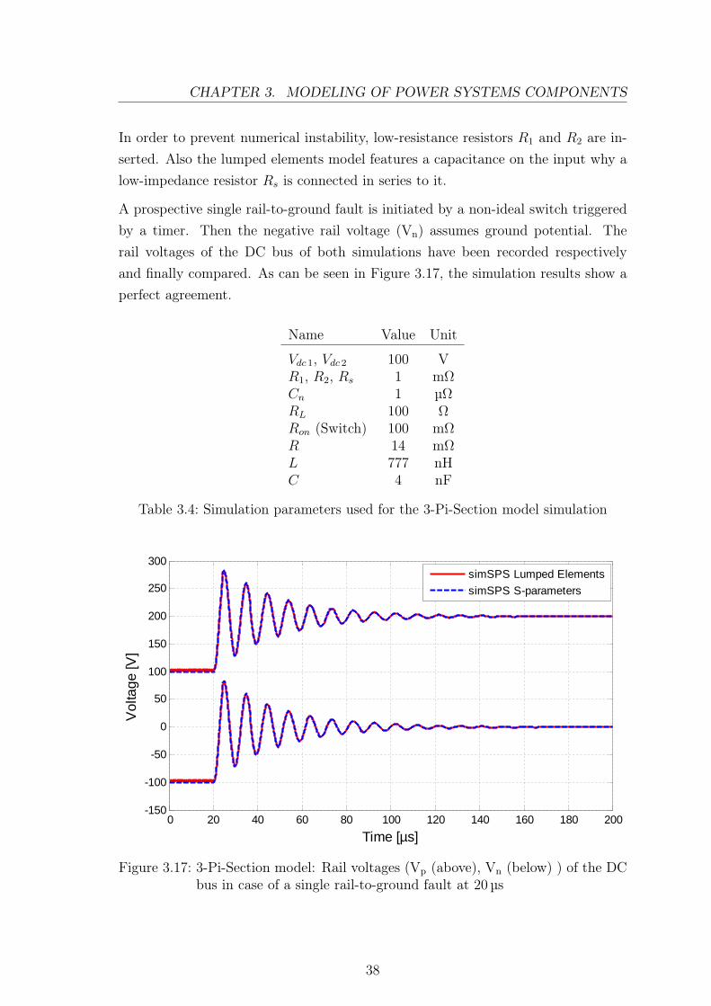
CHAPTER 3. MODELING OF POWER SYSTEMS COMPONENTS
In order to prevent numerical instability, low-resistance resistors R1 and R2 are in-serted. Also the lumped elements model features a capacitance on the input why alow-impedance resistor Rs is connected in series to it.
A prospective single rail-to-ground fault is initiated by a non-ideal switch triggeredby a timer. Then the negative rail voltage (Vn) assumes ground potential. Therail voltages of the DC bus of both simulations have been recorded respectivelyand finally compared. As can be seen in Figure 3.17, the simulation results show aperfect agreement.
Name Value Unit
Vdc 1, Vdc 2 100 VR1, R2, Rs 1 mΩCn 1 µΩRL 100 ΩRon (Switch) 100 mΩR 14 mΩL 777 nHC 4 nF
Table 3.4: Simulation parameters used for the 3-Pi-Section model simulation
0 20 40 60 80 100 120 140 160 180 200-150
-100
-50
0
50
100
150
200
250
300
Time [µs]
Vol
tage
[V]
simSPS Lumped Elements
simSPS S-parameters
Figure 3.17: 3-Pi-Section model: Rail voltages (Vp (above), Vn (below) ) of the DCbus in case of a single rail-to-ground fault at 20 µs
38
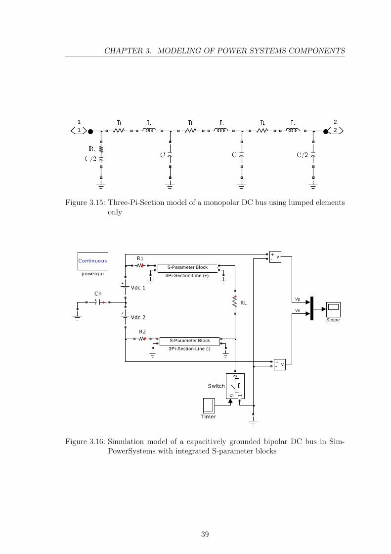
CHAPTER 3. MODELING OF POWER SYSTEMS COMPONENTS
2
2
1
1
Figure 3.15: Three-Pi-Section model of a monopolar DC bus using lumped elementsonly
Continuous
powergui
v+-
v+-
Vdc 2
Vdc 1
Timer
g 12
Switch
Scope
+
RL
+
R2
+
R1
+
Cn
S-Parameter Block
3Pi-Section-Line (-)
S-Parameter Block
3Pi-Section-Line (+)
Vn
Vp
Figure 3.16: Simulation model of a capacitively grounded bipolar DC bus in Sim-PowerSystems with integrated S-parameter blocks
39
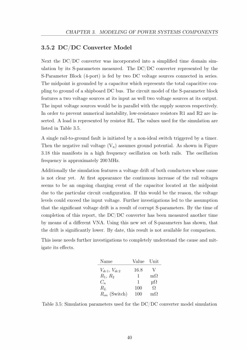
CHAPTER 3. MODELING OF POWER SYSTEMS COMPONENTS
3.5.2 DC/DC Converter Model
Next the DC/DC converter was incorporated into a simplified time domain sim-ulation by its S-parameters measured. The DC/DC converter represented by theS-Parameter Block (4-port) is fed by two DC voltage sources connected in series.The midpoint is grounded by a capacitor which represents the total capacitive cou-pling to ground of a shipboard DC bus. The circuit model of the S-parameter blockfeatures a two voltage sources at its input as well two voltage sources at its output.The input voltage sources would be in parallel with the supply sources respectively.In order to prevent numerical instability, low-resistance resistors R1 and R2 are in-serted. A load is represented by resistor RL. The values used for the simulation arelisted in Table 3.5.
A single rail-to-ground fault is initiated by a non-ideal switch triggered by a timer.Then the negative rail voltage (Vn) assumes ground potential. As shown in Figure3.18 this manifests in a high frequency oscillation on both rails. The oscillationfrequency is approximately 200 MHz.
Additionally the simulation features a voltage drift of both conductors whose causeis not clear yet. At first appearance the continuous increase of the rail voltagesseems to be an ongoing charging event of the capacitor located at the midpointdue to the particular circuit configuration. If this would be the reason, the voltagelevels could exceed the input voltage. Further investigations led to the assumptionthat the significant voltage drift is a result of corrupt S-parameters. By the time ofcompletion of this report, the DC/DC converter has been measured another timeby means of a different VNA. Using this new set of S-parameters has shown, thatthe drift is significantly lower. By date, this result is not available for comparison.
This issue needs further investigations to completely understand the cause and mit-igate its effects.
Name Value Unit
Vdc 1, Vdc 2 16.8 VR1, R2 1 mΩCn 1 µΩRL 100 ΩRon (Switch) 100 mΩ
Table 3.5: Simulation parameters used for the DC/DC converter model simulation
40
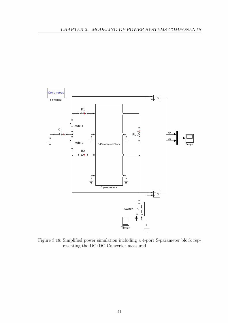
CHAPTER 3. MODELING OF POWER SYSTEMS COMPONENTS
Continuous
powerguiv
+-
v+-
Vdc 2
Vdc 1
Timer
g 12
Switch
ScopeS-Parameter Block
S parameters
+
RL
+
R2
+
R1
+
Cn
Vn
Vp
Figure 3.18: Simplified power simulation including a 4-port S-parameter block rep-resenting the DC/DC Converter measured
41
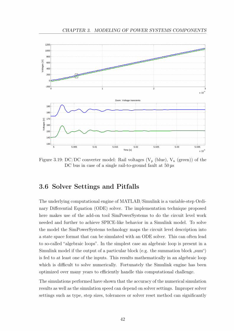
CHAPTER 3. MODELING OF POWER SYSTEMS COMPONENTS
0 1 2 3
x 10-4
-200
0
200
400
600
800
1000
1200V
olta
ges
[V]
5 5.005 5.01 5.015 5.02 5.025 5.03 5.035
x 10-5
130
140
150
160
170
180
190
Zoom: Voltage transients
Time [s]
Vol
tage
s [V
]
Figure 3.19: DC/DC converter model: Rail voltages (Vp (blue), Vn (green)) of theDC bus in case of a single rail-to-ground fault at 50 µs
3.6 Solver Settings and Pitfalls
The underlying computational engine of MATLAB/Simulink is a variable-step Ordi-nary Differential Equation (ODE) solver. The implementation technique proposedhere makes use of the add-on tool SimPowerSystems to do the circuit level workneeded and further to achieve SPICE-like behavior in a Simulink model. To solvethe model the SimPowerSystems technology maps the circuit level description intoa state space format that can be simulated with an ODE solver. This can often leadto so-called “algebraic loops”. In the simplest case an algebraic loop is present in aSimulink model if the output of a particular block (e.g. the summation block „sum“)is fed to at least one of the inputs. This results mathematically in an algebraic loopwhich is difficult to solve numerically. Fortunately the Simulink engine has beenoptimized over many years to efficiently handle this computational challenge.
The simulations performed have shown that the accuracy of the numerical simulationresults as well as the simulation speed can depend on solver settings. Improper solversettings such as type, step sizes, tolerances or solver reset method can significantly
42
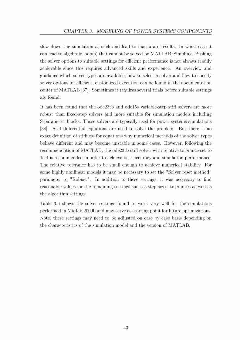
CHAPTER 3. MODELING OF POWER SYSTEMS COMPONENTS
slow down the simulation as such and lead to inaccurate results. In worst case itcan lead to algebraic loop(s) that cannot be solved by MATLAB/Simulink. Pushingthe solver options to suitable settings for efficient performance is not always readilyachievable since this requires advanced skills and experience. An overview andguidance which solver types are available, how to select a solver and how to specifysolver options for efficient, customized execution can be found in the documentationcenter of MATLAB [37]. Sometimes it requires several trials before suitable settingsare found.
It has been found that the ode23tb and ode15s variable-step stiff solvers are morerobust than fixed-step solvers and more suitable for simulation models includingS-parameter blocks. Those solvers are typically used for power systems simulations[38]. Stiff differential equations are used to solve the problem. But there is noexact definition of stiffness for equations why numerical methods of the solver typesbehave different and may become unstable in some cases. However, following therecommendation of MATLAB, the ode23tb stiff solver with relative tolerance set to1e-4 is recommended in order to achieve best accuracy and simulation performance.The relative tolerance has to be small enough to achieve numerical stability. Forsome highly nonlinear models it may be necessary to set the "Solver reset method"parameter to "Robust". In addition to these settings, it was necessary to findreasonable values for the remaining settings such as step sizes, tolerances as well asthe algorithm settings.
Table 3.6 shows the solver settings found to work very well for the simulationsperformed in Matlab 2009b and may serve as starting point for future optimizations.Note, these settings may need to be adjusted on case by case basis depending onthe characteristics of the simulation model and the version of MATLAB.
43
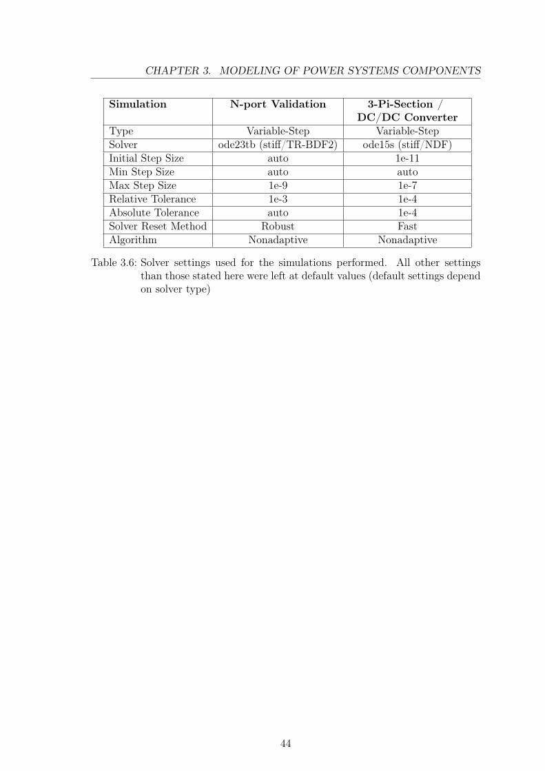
CHAPTER 3. MODELING OF POWER SYSTEMS COMPONENTS
Simulation N-port Validation 3-Pi-Section /DC/DC Converter
Type Variable-Step Variable-StepSolver ode23tb (stiff/TR-BDF2) ode15s (stiff/NDF)Initial Step Size auto 1e-11Min Step Size auto autoMax Step Size 1e-9 1e-7Relative Tolerance 1e-3 1e-4Absolute Tolerance auto 1e-4Solver Reset Method Robust FastAlgorithm Nonadaptive Nonadaptive
Table 3.6: Solver settings used for the simulations performed. All other settingsthan those stated here were left at default values (default settings dependon solver type)
44
4 Conclusion
One subtask within the Electric Ship Research and Development Consortium (ES-RDC) effort focuses on grounding aspects of direct current (DC) systems operatedat medium voltage (MVDC). One of the research thrusts is the transient behavior ofthe DC bus as a function of the location of a prospective single rail-to-ground fault.For higher accuracy, specific models of the system components might be required,which are tailored to grounding studies in shipboard power systems. At the Centerfor Advanced Power Systems ongoing research is concerned with the characterizationof common components of a 3-phase power system based on S-parameters.
In this work S-parameter models have been introduced for transient power systemsmodeling. A method has been proposed how to incorporate S-Parameters in powersystems software packages. A S-parameters block has been built which allows tostudy common components of a shipboard power system. Validation based on stepresponse has been conducted using Agilent Advanced Design System (ADS). It hasbeen shown that the technique proposed here is accurate, valuable and feasible forhigh-fidelity power system simulations. It has been found that the choice of solversettings are critical. In future it might be reasonable to focus on the cause moredetailed in order to possibly figure out whether there are certain indicators whichplay a part in contributing to the finding of proper solver settings. The empha-sis of S-parameters implementation is on Simulink/SimPowerSystems. Despite itis believed that the implementation method is suitable for the software packagePSCAD/EMTDC as well. Investigation has shown that this simulation tool sup-ports the integration of Nth order laplace domain transfer functions. Based on thisknowledge it needs to be vetted if this tool provides the opportunity (as MATLAB)to programmatically (based on scripts) integrate a simulation model into a timedomain simulation.
A complete S-parameters characterization of power electronics components of agrounding testbed by Purdue University has been conducted by means of a 2-portvector network analyzer (VNA). The measurements were carried out in collaborationwith the National High Magnetic Field Laboratory (NHMFL). It has been shown
45
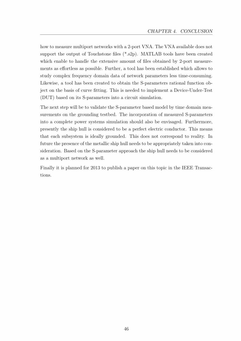
CHAPTER 4. CONCLUSION
how to measure multiport networks with a 2-port VNA. The VNA available does notsupport the output of Touchstone files (*.s2p). MATLAB tools have been createdwhich enable to handle the extensive amount of files obtained by 2-port measure-ments as effortless as possible. Further, a tool has been established which allows tostudy complex frequency domain data of network parameters less time-consuming.Likewise, a tool has been created to obtain the S-parameters rational function ob-ject on the basis of curve fitting. This is needed to implement a Device-Under-Test(DUT) based on its S-parameters into a circuit simulation.
The next step will be to validate the S-parameter based model by time domain mea-surements on the grounding testbed. The incorporation of measured S-parametersinto a complete power systems simulation should also be envisaged. Furthermore,presently the ship hull is considered to be a perfect electric conductor. This meansthat each subsystem is ideally grounded. This does not correspond to reality. Infuture the presence of the metallic ship hull needs to be appropriately taken into con-sideration. Based on the S-parameter approach the ship hull needs to be consideredas a multiport network as well.
Finally it is planned for 2013 to publish a paper on this topic in the IEEE Transac-tions.
46
CHAPTER 4. CONCLUSION
Generator3-port
AC cable (bus)6-port
Rectifier5-port
DC cable (bus)4-port
DC/DC converter4-port
DC cable (bus)4-port
Inverter5-port
Motor3-port
VNA VNAADS/MATLAB VNAVNAVNA ADS/MATLAB ADS/MATLAB
Maybe another cable?
Completed in 2012
Planned for 2013
(a) Each device ideally grounded
Generator4-port
AC cable (bus)6-port
Rectifier6-port
DC cable (bus)4-port
DC/DC converter5-port
DC cable (bus)4-port
Inverter6-port
Motor4-port
Ship hull
5-port
Super ground(e.g. sea water, port connection)
VNAVNAVNA ADS/MATLAB VNA VNA
COMSOL or ADS
ADS/MATLABADS/MATLAB
(b) Each device locally grounded to ship hull
Figure 4.1: Characterization of common shipboard power systems components basedon S-parameters. Presently ship hull is considered to be a perfect electricconductor (above). Considering the presence of the metallic ship hullresults in an additional port of the system components (below).
47

List of Figures
1.1 Simplified shipboard power system comparing a conventional design(above) with a design based on IPS (below) [4, modified] . . . . . . . 5
1.2 Next Generation Integrated Power System (NGIPS) Technology De-velopment Roadmap. The DDG-1000 destroyer is the poster child forthe U.S. to shift to all-electric ships. [10, modified] . . . . . . . . . . 6
2.1 Simplified DC distribution system showing four different locations forpotential faults (arrow 1 to 4) [15] . . . . . . . . . . . . . . . . . . . . 10
2.2 Transient phenomena and system offset for a high grounding impedance[15] . . . . . . . . . . . . . . . . . . . . . . . . . . . . . . . . . . . . 10
2.3 Common components of a simplified power system considered as mul-tiport (N-port) networks. Ship hull is treated to be a perfect conduc-tor. [15, modified] . . . . . . . . . . . . . . . . . . . . . . . . . . . . . 12
3.1 Arbitrary N-port network with ai and bi as the incident and reflectedwaves. Vs and Zs are the source voltage and source impedance. ZLis the port termination equal to the source impedance. Vi is thepotential difference between the ith-port and a reference (e.g. GND).Ii is the current flow through the interface of port i and the load orsource. The reference planes are denoted as tx. . . . . . . . . . . . . 16
3.2 2-port vector network analyzer (VNA) Agilent 8753ES available atthe National High Magnetic Field Laboratory (NHMFL) [30] . . . . . 20
3.3 Measurement system for s11 and s21 S-parameters using a two-portnetwork analyzer [19] . . . . . . . . . . . . . . . . . . . . . . . . . . . 21
3.4 2×2 submatrices of a 4-port network. Each submatrix is representedby a square with corners at the locations of the four submatrix ele-ments in the complete 4× 4 S-matrix [31, modified] . . . . . . . . . . 23
48
LIST OF FIGURES
3.5 Different measurement combinations of a 4-port Network using a 2-port VNA. The matrices contain the corresponding S-parameters ob-tained by each measurement respectively. . . . . . . . . . . . . . . . . 24
3.6 Power electronics of the experimental small-scale testbed used forgrounding studies at Purdue University. DC/DC converter (left) andDC/AC inverter (right) after the preparation with mounted RF con-nectors (Type N-connectors) . . . . . . . . . . . . . . . . . . . . . . 26
3.7 Measurements of the reflection coefficient s33 of the DC/DC converterwith enclosure. s33←14 denotes the reflection measured when port 1and 4 are terminated. s33←12 denotes the reflection measured whenport 1 and 2 are terminated and so on. . . . . . . . . . . . . . . . . 27
3.8 Measured transmission coefficient s34 of the DC/DC converter withand without enclosure . . . . . . . . . . . . . . . . . . . . . . . . . . 28
3.9 Comparison between the frequency response of the rational functionobject and that of the original data [34] . . . . . . . . . . . . . . . . . 31
3.10 Simulink model for a rational function representing a single S-parameter 32
3.11 S-parameter model block build in Simulink/SimPowerSystems. Arbi-trary complex passive and active sources and loads can be incorpo-rated around the S-parameters model block . . . . . . . . . . . . . . . 33
3.12 Internals of the S-parameters block which implement the equationsthat relate the four S-parameters to the input and output port voltageand current. . . . . . . . . . . . . . . . . . . . . . . . . . . . . . . . 34
3.13 Validation circuit designed in ADS consiting of two single∏-Section
representing two single-phase transmission lines. Those are cross-coupled by two capacitors which leads to a four-port network config-uration. . . . . . . . . . . . . . . . . . . . . . . . . . . . . . . . . . . 35
3.14 Step response of the 4-port network used for the validation process . 36
3.17 3-Pi-Section model: Rail voltages (Vp (above), Vn (below) ) of theDC bus in case of a single rail-to-ground fault at 20 µs . . . . . . . . . 38
3.15 Three-Pi-Section model of a monopolar DC bus using lumped ele-ments only . . . . . . . . . . . . . . . . . . . . . . . . . . . . . . . . . 39
3.16 Simulation model of a capacitively grounded bipolar DC bus in Sim-PowerSystems with integrated S-parameter blocks . . . . . . . . . . 39
49
LIST OF FIGURES
3.18 Simplified power simulation including a 4-port S-parameter block rep-resenting the DC/DC Converter measured . . . . . . . . . . . . . . . 41
3.19 DC/DC converter model: Rail voltages (Vp (blue), Vn (green)) of theDC bus in case of a single rail-to-ground fault at 50 µs . . . . . . . . . 42
4.1 Characterization of common shipboard power systems componentsbased on S-parameters. Presently ship hull is considered to be aperfect electric conductor (above). Considering the presence of themetallic ship hull results in an additional port of the system compo-nents (below). . . . . . . . . . . . . . . . . . . . . . . . . . . . . . . . 47
A.1 Screenshot of the \\plasma\STUDENT\kofler directory at the PLASMAServer at CAPS . . . . . . . . . . . . . . . . . . . . . . . . . . . . . . 57
B.1 Screenshot of the main GUI recommended to execute the tools estab-lished . . . . . . . . . . . . . . . . . . . . . . . . . . . . . . . . . . . . 58
B.2 GUI of rational fitting tool available to build the S-parameter rationalfunction models . . . . . . . . . . . . . . . . . . . . . . . . . . . . . . 60
B.3 GUI of the plot tool available to plot the S-parameters data . . . . . 62
B.4 GUI of the tool to generate the Touchstone files of the measurementsobtained witht the 2-port VNA at the National High Magnetic FieldLaboratory (NHMFL) . . . . . . . . . . . . . . . . . . . . . . . . . . 64
B.5 GUI of the tool available to assemble the partial 2-port measurementsto a Touchstone file which contains the N-port S-parameters . . . . . 66
C.1 Screenshot of the mask of the S-parameters block on the top-level . . 68
C.2 Screenshot of the mask of the S-parameter transfer function blocks . 68
C.3 Screenshot of the „Parameter“ tab in the mask editor of the S-parametersblock . . . . . . . . . . . . . . . . . . . . . . . . . . . . . . . . . . . 69
C.4 Screenshot of the „Initialization“ tab in the mask editor of the S-parameter transfer function blocks . . . . . . . . . . . . . . . . . . . 69
C.5 Screenshot of the model properties defined in Simulink . . . . . . . . 70
50
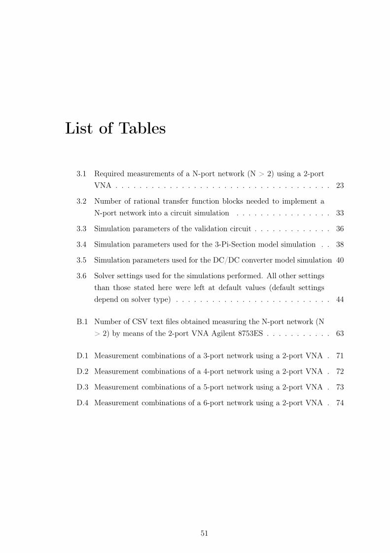
List of Tables
3.1 Required measurements of a N-port network (N > 2) using a 2-portVNA . . . . . . . . . . . . . . . . . . . . . . . . . . . . . . . . . . . . 23
3.2 Number of rational transfer function blocks needed to implement aN-port network into a circuit simulation . . . . . . . . . . . . . . . . 33
3.3 Simulation parameters of the validation circuit . . . . . . . . . . . . . 36
3.4 Simulation parameters used for the 3-Pi-Section model simulation . . 38
3.5 Simulation parameters used for the DC/DC converter model simulation 40
3.6 Solver settings used for the simulations performed. All other settingsthan those stated here were left at default values (default settingsdepend on solver type) . . . . . . . . . . . . . . . . . . . . . . . . . . 44
B.1 Number of CSV text files obtained measuring the N-port network (N> 2) by means of the 2-port VNA Agilent 8753ES . . . . . . . . . . . 63
D.1 Measurement combinations of a 3-port network using a 2-port VNA . 71
D.2 Measurement combinations of a 4-port network using a 2-port VNA . 72
D.3 Measurement combinations of a 5-port network using a 2-port VNA . 73
D.4 Measurement combinations of a 6-port network using a 2-port VNA . 74
51
Bibliography
[1] B. Wagner, “All-Electric Ship Could Begin to Take Shape By 2012,” NationalDefense Magazine, Archive Nov. 2007.
[2] P. B. Backlund, C. C. Seepersad, and T. M. Kiehne, “A System-Level DesignFramework for All-Electric Ship Thermal Systems,” American Society of NavalEngineers, 2012.
[3] N. H. Doerry and J.C. Davis, “Integrated Power System for Marine Applica-tions,” Naval Engineers Journal, May 1994.
[4] T.J. McCoy, “Trends in ship electric propulsion,” Power Engineering SocietySummer Meeting, 2002 IEEE, vol. 1, pp. 343–346, Jul 2002.
[5] G. Buja, A. da Rin, R. Menis, and G. Sulligoi, “Dependable Design Assess-ment of Integrated Power Systems fo All Electric Ships,” Electrical Systems forAircraft, Railway and Ship Propulsion (ESARS),, pp. 1–8, 19-21 Oct. 2010.
[6] Capt. N. Doerry. Open Architecture Approach for the NextGeneration Integrated Power System. [Online]. Available: https://www.navalengineers.org/SiteCollectionDocuments/2007%20Proceedings%20Documents/Automation%20and%20Controls%202007/1-2-9%20Paper.pdf
[7] L. HanYu and M. LongHua, “Integrated Protection on Shipboard IntegratedPower System,” The International Conference on Advanced Power System Au-tomation and Protection (APAP), vol. 1, pp. 252–255, 16-20 Oct. 2011.
[8] V. R. Basam and A. Das, “All Electric Ship-The Super Platform for Tomor-row’s Naval Warfare,” Second International Seminar And Exhibition on NavalArmaments (NAVARMS), 2010.
[9] K. P. Logan, “Intelligent Diagnostic Requirements of Future All-ElectricShip Integrated Power System,” IEEE Transactions on Industry Applications,vol. 43, no. 1, pp. 151–163, Jan. 2007.
[10] N. Doerry, “Next Generation Integrated Power Systems for the Future Fleet,”IEEE Electric Ship Technologies Symposium, Baltimore, Apr. 2009.
52
BIBLIOGRAPHY
[11] B. Jacobson and J. Walker, “Grounding Considerations for DC and Mixed DCand AC Power Systems,” Society of Naval Engineers Journal, vol. 119, no. 2,pp. 49–62, 2007.
[12] IEEE Std. 45, “IEEE Recommended Practice for Electrical Installations onShipboard,” pp. 1–91, 2011.
[13] IEEE Ste 142 (Green Book), “IEEE Recommended Practice for Grounding ofIndustrial and Commercial Power Systems,” 1982.
[14] Y. Nyanteh, L. Graber, C. Edrington, S. Srivastava, and D. Cartes, “Overviewof Simulation Models for Partial Discharge and Electrical Treeing to DetermineFeasibility for Estimation of Remaining Life of Machine Insulation Systems,”Electrical Insulation Conference (EIC), pp. 327–332, Jun. 2011.
[15] D. Lee, D. Infante, J. Langston, S. V. Poroseva, M. Steurer, and T. Bald-win, “Grounding Studies in a Medium Voltage DC Shipboard Power Systemwith Uncertain Parameters,” Conference on Grand Challenges in Modeling &Simulation, pp. 113–120, 2010.
[16] D. Infante, J. Langston, L. Graber, and M. Steurer, “Guiding the Selection ofPhysical Experiments Suporting Validation of Electric Power System Models,”Conference on Grand Challenges in Modeling & Simulation, pp. 173–180, 2011.
[17] L. Graber, D. Infante, M. Steurer, and W.W. Brey, “Validation of Cable Mod-els for Simulation of Transients in Shipboard Power Systems,” High VoltageEngineering, vol. 37, no. 11, pp. 2836–2842, 2011.
[18] V. Cecchi, A. Leger, and K. Miu, “Modeling approach for transmission linesin the presence of non-fundamental frequencies,” IEEE Transactions on PowerDelivery, vol. 24, no. 4, pp. 2328–2335, 2009.
[19] R. Ludwig and P. Bretchko, RF Circuit Design: Theory and Applications. Up-per Saddle River: Prentice Hall, 2000.
[20] D. M. Pozar, Microwave and RF Design of Wireless Systems. New York andChichester: Wiley, 2000.
[21] J. A. Dobrowolski, Microwave Network Design Using the Scattering Matrix.Boston: Artech House, 2010.
[22] K. Kurokawa, “Power Waves and the Scattering Matrix,” IEEE Transactionson Microwave Theory and Techniques, vol. 13, no. 2, pp. 194–202, Mar 1965.
53
BIBLIOGRAPHY
[23] E.W. Matthews, “The Use of Scattering Matrices in Microwave Circuits,” IRETransactions on Microwave Theory and Techniques, vol. 3, pp. 21–26, Apr.1955.
[24] R. Mavaddat, Network Scattering Parameters. Singapore and River Edge andN.J: World Scientific, 1996.
[25] A. I. Khalil and M. B. Steer, “A Generalized Scattering Matrix Method Usingthe Method of Moments for Electromagnetic Analysis of Multilayered Struc-tures in Waveguide: IEEE Transactions on Microwave Theory and Techniques,”vol. 47, no. 11, pp. 2151–2157, Nov. 1999.
[26] L. G. Maloratsky, Passive RF & Microwave Integrated Circuits. Amsterdamand and Bosto: Elsevier/Newnes, 2004.
[27] S. Ramo, J. Whinnery, and T. van Duzer, Fields and Waves in CommunicationElectronics, 3rd ed. New York: John Wiley & Sons, 1994.
[28] D. A. Frickey, “Conversions Between S, Z, Y, h, ABCD, and T Parameterswhich are Valid for Complex Source and Load Impedances,” IEEE Transactionson Microwave Theory and Techniques, vol. 42, no. 2, pp. 205–211, Feb 1994.
[29] EIA/IBIS Open Forum, “Touchstone File Format Specification: Rev. 1.1,” 2002.
[30] VNA Agilent 8753ES. [Online]. Available: http://www.testunlimited.com/images/products/agilent_8753es.jpg
[31] J.C. Tippet and R.A. Speciale, “A Rigorous Technique for Measuring the Scat-tering Matrix of a Multiport Device with a 2-Port Network Analyzer,” IEEETransactions on Microwave Theory and Techniques, vol. 30, no. 5, pp. 661–666,May 1982.
[32] The MathWorks Inc. Matlab 7.9.1 (R2009b) Service Pack 1. (2012). [Online].Available: http://www.mathworks.com
[33] B. Gustavsen and A. Semlyen, “Rational approximation of frequency domainresponses by vector fitting,” IEEE Trans. Power Delivery, vol. 14, no. 3, pp.1051–1061, Jul 1999.
[34] R. Zeng and J. Sinsky, “Modified Rational Function Modeling Technique forHigh Speed Circuits,” IEEE MTT-S Int. Microwave Microwave SymposiumDigest, pp. 1951–1954, Jun 2006.
[35] L. W. Nagel and D.O. Pederson. (April 1973) SPICE (SimulationProgram with Integrated Circuit Emphasis). [Online]. Available: http://www.eecs.berkeley.edu/Pubs/TechRpts/1973/22871.html
54

BIBLIOGRAPHY
[36] Agilent Design Software ADS 2011.10. (2012). [Online]. Avail-able: http://www.home.agilent.com/agilent/software.jspx?ckey=2212036&lc=eng&cc=US&nid=-34335.0&id=2212036&pageMode=PV
[37] The MathWorks. (2012) Documentation Center. [Online]. Available: http://www.mathworks.com/help
[38] K. Schoder. Center for Advanced Power Systems (CAPS). Private Communi-cation.
55
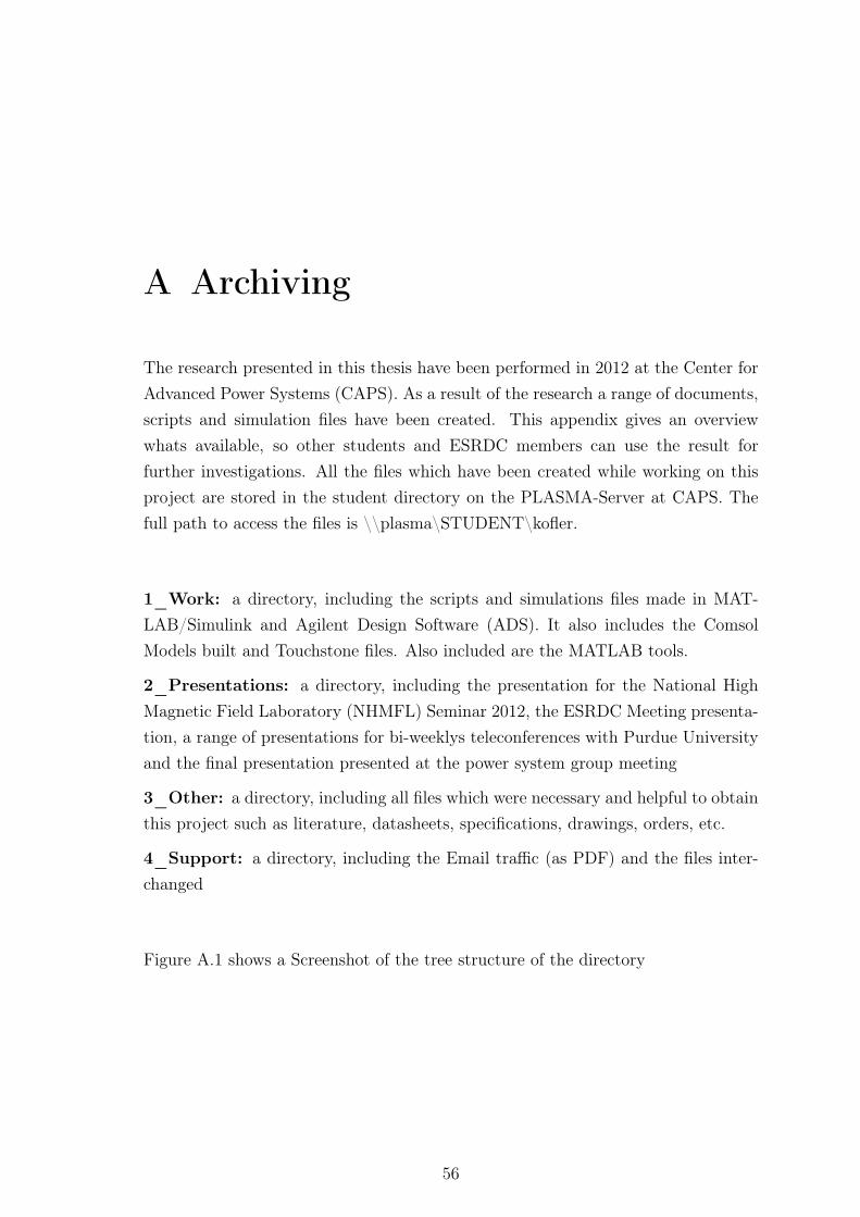
A Archiving
The research presented in this thesis have been performed in 2012 at the Center forAdvanced Power Systems (CAPS). As a result of the research a range of documents,scripts and simulation files have been created. This appendix gives an overviewwhats available, so other students and ESRDC members can use the result forfurther investigations. All the files which have been created while working on thisproject are stored in the student directory on the PLASMA-Server at CAPS. Thefull path to access the files is \\plasma\STUDENT\kofler.
1_Work: a directory, including the scripts and simulations files made in MAT-LAB/Simulink and Agilent Design Software (ADS). It also includes the ComsolModels built and Touchstone files. Also included are the MATLAB tools.
2_Presentations: a directory, including the presentation for the National HighMagnetic Field Laboratory (NHMFL) Seminar 2012, the ESRDC Meeting presenta-tion, a range of presentations for bi-weeklys teleconferences with Purdue Universityand the final presentation presented at the power system group meeting
3_Other: a directory, including all files which were necessary and helpful to obtainthis project such as literature, datasheets, specifications, drawings, orders, etc.
4_Support: a directory, including the Email traffic (as PDF) and the files inter-changed
Figure A.1 shows a Screenshot of the tree structure of the directory
56
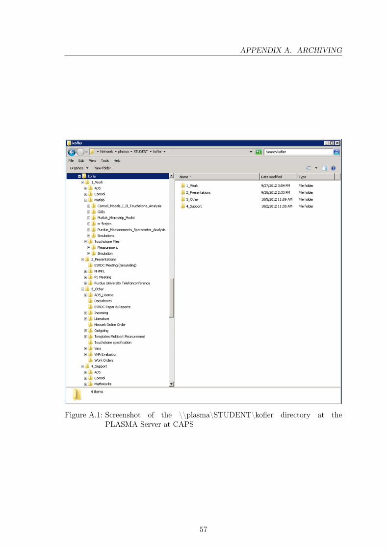
APPENDIX A. ARCHIVING
Figure A.1: Screenshot of the \\plasma\STUDENT\kofler directory at thePLASMA Server at CAPS
57
B Matlab Tools
This appendix is a comprehensive summary of the implemented tools needed inthis work for modelling S-parameters and helpful for the frequent approach of S-parameters analysis. Four Graphical User Interfaces (GUIs) have been establishedwhose particular tasks will be described in the following. The interfaces can befound in the directory \\plasma\1_Work\Matlab\GUIs.
B.1 Main GUI
It is recommended to execute the individual GUIs by the main GUI shown in FigureB.1. This GUI can be executed either by the OpenGUI.m or the stand-alone appli-cation GUIs_CAPS.exe located in the EXE folder. Note that the latter requires ainstalled version (version 7.15 or higher) of the Matlab Compiler Runtime (MCR).
Remark: In case of not using the stand-alone application, the tools created requirean installed version of the RF toolbox (Version 2.6 (Matlab 2009) or higher).
Figure B.1: Screenshot of the main GUI recommended to execute the tools estab-lished
58
APPENDIX B. MATLAB TOOLS
B.2 Rational Fitting for S-parameters Transfer
Functions
Description
Figure B.2 shows the Matlab GUI for the rational fitting process needed to buildthe S-parameters rational function models. The fitting algorithm used fits a rationalfunction model to the complex input data over the specified frequencies. The inputdata is stored in a Touchstone file that contains N-port S-parameters. The importantinput parameters which need to be specified are the error (fitting) tolerance [dB]tol, the asymptotic behavior of the fit tendstozero, the Delay Factor delayfactorand the number of poles npoles. The result of the approximation is a <NxNrfmodel.rational> object with the properties A (poles), C (residues), D and Delay.It also determines the number and order of transfer function blocks for each S-parameter needed. Finally the fit can be stored in a MAT-file (*.mat).
How To Use
1. Add the Touchstone file that contains N-port S-parameters (*.sNp).
2. Press the button „Get Data“ to load the complex data.
3. Specify the rational fitting parameters values. The default values do the jobvery well in many cases but may need to be adjusted on a case by case basis.Stipulating the tolerance and poles manually may results in that the numberof poles does not gain the desired tolerance. Typically used if one has a goodidea of the order of the system (e.g. lumped element models). To obtain anaccurate fit, it is a rule of thumb to chose the number of poles greater than orat least equal to twice the number of observable peaks on a plot of the data inthe frequency domain. Stipulating the tolerance and set the number of polesto [] (bracket) and let the fitting algorithm determine the required order of thesystem is typically used for measurement data on distributed systems whereguessing the order requires some skill. It typically results in more transferfunction blocks (stages).
4. Apply fit to the input data. The fit can be applied to all N-port S-parametersautomatically using the same input parameter values by checking the Check-box „Fit all“. Otherwise the S-parameters can be fitted manually using differentinput parameter values for each S-parameter.
5. Save the rational function object to a MAT-file (*.mat). The rational functionobject can only be saved if the fit is applied to all N2 S-parameters.
59
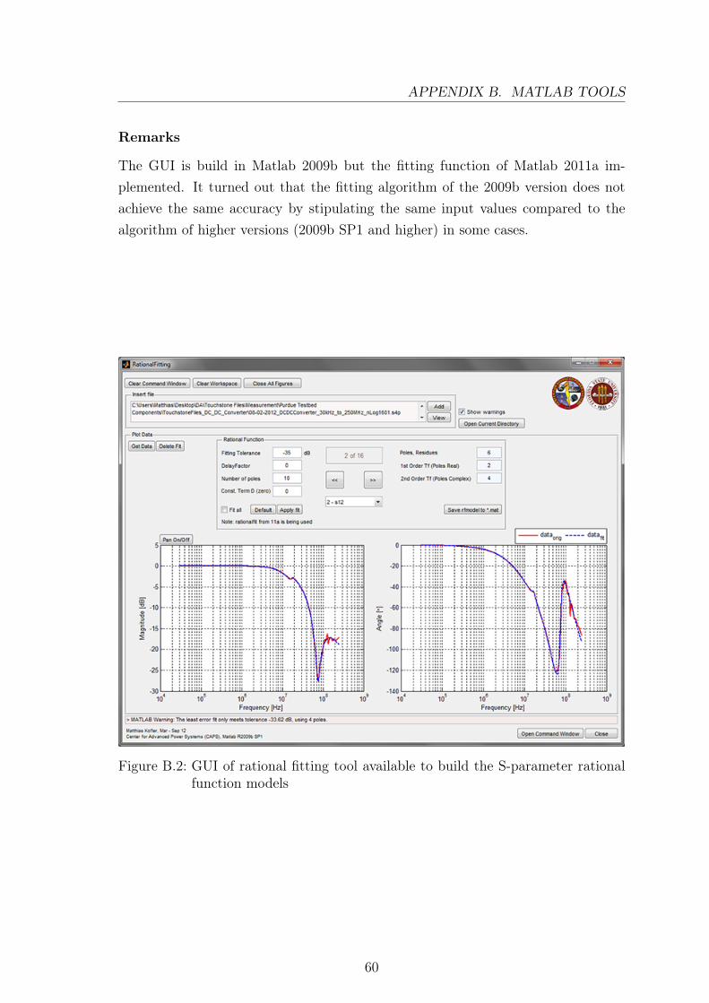
APPENDIX B. MATLAB TOOLS
Remarks
The GUI is build in Matlab 2009b but the fitting function of Matlab 2011a im-plemented. It turned out that the fitting algorithm of the 2009b version does notachieve the same accuracy by stipulating the same input values compared to thealgorithm of higher versions (2009b SP1 and higher) in some cases.
Figure B.2: GUI of rational fitting tool available to build the S-parameter rationalfunction models
60
APPENDIX B. MATLAB TOOLS
B.3 Graphical Representation of S-parameters
Description
The interpretation of S-parameters is an important and frequent concern. To achievethis in a simple and less time-consuming manner, a tool has been established whichallows to plot S-parameters data in a very efficient fashion. The tool not only allowsto plot S-parameter data but also alternative network parameters such as Z- orY-parameters. It provides the capability to display the input data in linear andlogarithmic form as well as in polar coordinates (S-parameters only). In particularit may be sufficient to plot just a few of the network parameters. This can bedone by checking the checkbox of the corresponding network parameter. Whereasthe number of added files is equivalent to the number of line objects in one figurepresent respectively, the number of figures in total which will be created is dependon the network parameters chosen. In addition to this, the tool offers a couple ofsettings to specify the most important plot properties. The properties set are appliedto a selected line object in all figures present. In order to prevent the addition ofTouchstone Files with distinct extension and hence a possible mismatch due to adifferent number of N-port S-parameters, a filter has been implemented. The filteris set once the selection in the Panel „Select Network“ is made. On top of this thefigures opened can be saved.
How To Use
1. Select a network in the Panel „Select Network“ of which the network parame-ters are of interest.
2. Add the files that are to be plotted.
3. Choose the display form desired, the parameters as well as the format. Selectthe network parameter of interest (Checkboxes).
4. Optional: Define the plot properties.
5. To display the input data press „Plot“.
6. Optional: Press the button to save the figures opened.
Remarks
Some of the plot properties are applied on-the-fly to the figures and line objectspresent. The figures created are provided with an ID. In the event of saving thefigures present, figures of other Matlab entities will be excluded.
61
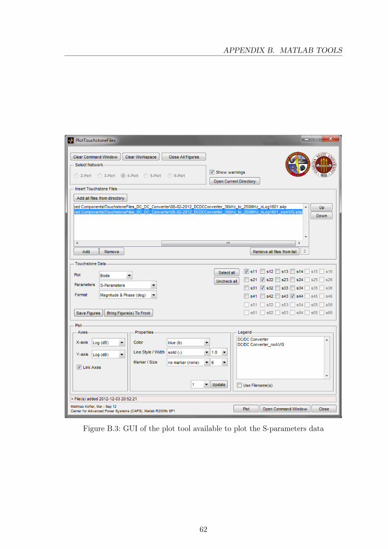
APPENDIX B. MATLAB TOOLS
Figure B.3: GUI of the plot tool available to plot the S-parameters data
62
APPENDIX B. MATLAB TOOLS
B.4 Generation of Touchstone File
Description
The Two-Port Vector Network Analyzer available at the National High MagneticField Laboratory (NHMFL) and used in this work does not support the output ofTouchstone Files. Instead the VNA exports each of the four S-parameters in a CSVtext file format respectively. For a single measurement performed this results in eight*.csv text files in total, since the magnitude and phase data is stored in separatefiles respectively. Following the approach to characterize a multiport network bymeans of a two-port VNA this results in a fairly large quantity of CSV files as canbe seen in table B.1.
N-port 2-port 3-port 4-port 5-port 6-portNumber of CSV files 8 24 48 80 120
Table B.1: Number of CSV text files obtained measuring the N-port network (N >2) by means of the 2-port VNA Agilent 8753ES
To obtain the Touchstone file(s) desired it would be very tedious and time-consumingto merge all the single files manually. To complete this task as effortless and fast aspossible, a tool has been established which makes the construction automatically.The only part which needs to be done manually is to insert the necessary files in thecorrect order. The result is a Touchstone file which meets the requirements definedin the specification [29].
How To Use
1. Choose the File Format (*.csv default)
2. Add the text files that contain the magnitude and phase data of the measuredS-parameters. It is important to insert the files in the right order (The defaultorder is displayed below the listbox).
3. In the Panel „Touchstone Files“ a couple of settings can be made such asthe Option Line desired. The Option Line defines the fashion in which theS-parameters finally stored in the Touchstone File. If everything is set asrequested, push the button „Write Touchstone File“ to generate the TouchstoneFile. Additonally a saving dialog appears which allows to save the generatedTouchstone File (.*s2p) in the chosen directory.
63
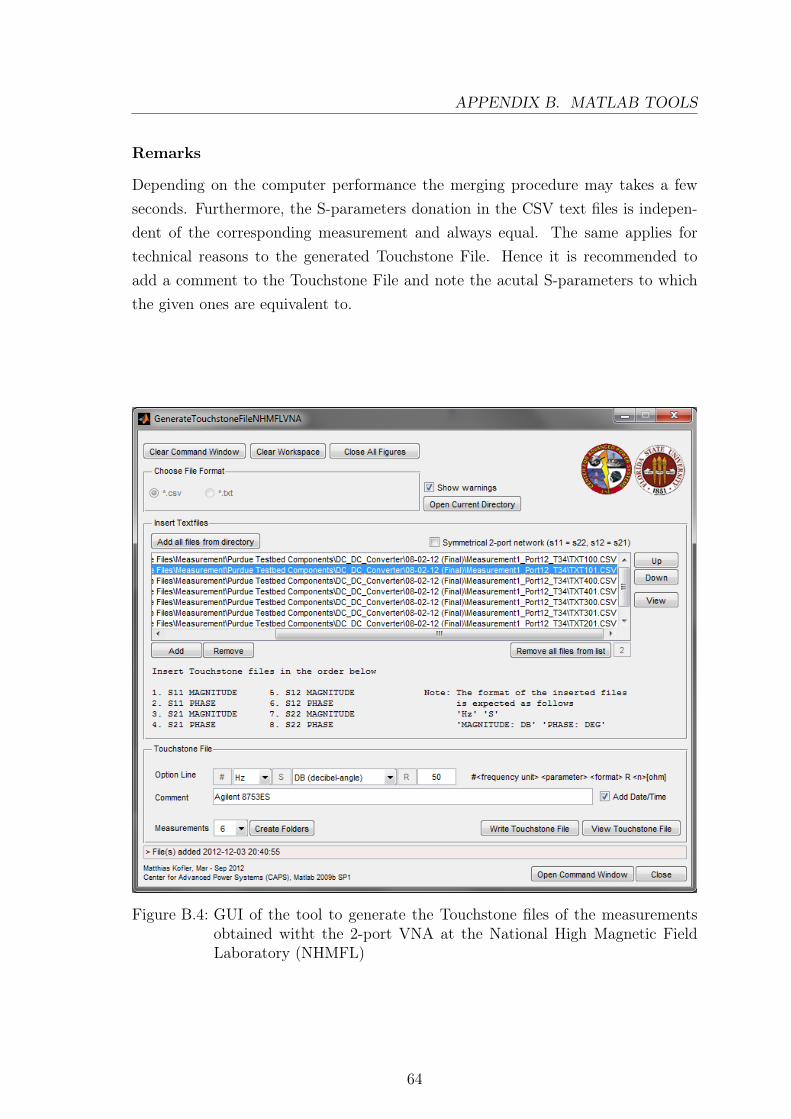
APPENDIX B. MATLAB TOOLS
Remarks
Depending on the computer performance the merging procedure may takes a fewseconds. Furthermore, the S-parameters donation in the CSV text files is indepen-dent of the corresponding measurement and always equal. The same applies fortechnical reasons to the generated Touchstone File. Hence it is recommended toadd a comment to the Touchstone File and note the acutal S-parameters to whichthe given ones are equivalent to.
Figure B.4: GUI of the tool to generate the Touchstone files of the measurementsobtained witht the 2-port VNA at the National High Magnetic FieldLaboratory (NHMFL)
64
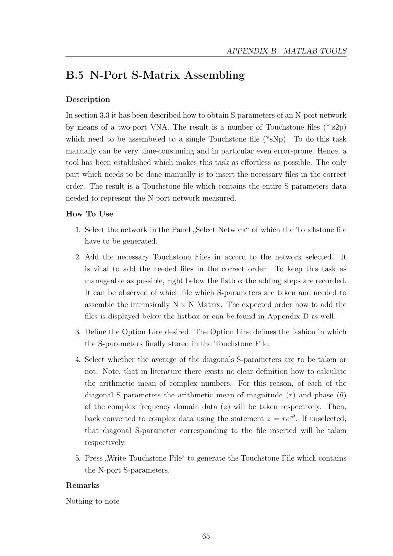
APPENDIX B. MATLAB TOOLS
B.5 N-Port S-Matrix Assembling
Description
In section 3.3 it has been described how to obtain S-parameters of an N-port networkby means of a two-port VNA. The result is a number of Touchstone files (*.s2p)which need to be assembeled to a single Touchstone file (*sNp). To do this taskmanually can be very time-consuming and in particular even error-prone. Hence, atool has been established which makes this task as effortless as possible. The onlypart which needs to be done manually is to insert the necessary files in the correctorder. The result is a Touchstone file which contains the entire S-parameters dataneeded to represent the N-port network measured.
How To Use
1. Select the network in the Panel „Select Network“ of which the Touchstone filehave to be generated.
2. Add the necessary Touchstone Files in accord to the network selected. Itis vital to add the needed files in the correct order. To keep this task asmanageable as possible, right below the listbox the adding steps are recorded.It can be observed of which file which S-parameters are taken and needed toassemble the intrinsically N × N Matrix. The expected order how to add thefiles is displayed below the listbox or can be found in Appendix D as well.
3. Define the Option Line desired. The Option Line defines the fashion in whichthe S-parameters finally stored in the Touchstone File.
4. Select whether the average of the diagonals S-parameters are to be taken ornot. Note, that in literature there exists no clear definition how to calculatethe arithmetic mean of complex numbers. For this reason, of each of thediagonal S-parameters the arithmetic mean of magnitude (r) and phase (θ)of the complex frequency domain data (z) will be taken respectively. Then,back converted to complex data using the statement z = rejθ. If unselected,that diagonal S-parameter corresponding to the file inserted will be takenrespectively.
5. Press „Write Touchstone File“ to generate the Touchstone File which containsthe N-port S-parameters.
Remarks
Nothing to note
65
APPENDIX B. MATLAB TOOLS
Figure B.5: GUI of the tool available to assemble the partial 2-port measurementsto a Touchstone file which contains the N-port S-parameters
66
C S-parameters Model Desription
This appendix gives an overview how the S-parameters block as such is implementedin Simulink/SimPowerSystems. Basically the model implementation features twosubsystems in total. One subsystem includes the transfer function blocks for eachS-parameter needed and the necessary blocks to implement the equations that relatethe S-parameters to the input and output port voltage(s) and current(s). Thissubsystem is represented by the S-parameters block on the top-level. The secondsubsystem represents the transfer function block for each S-parameter respectively.It contains the necessary blocks to implement the corresponding rational functionmodel respectively. The latter will be automatically built and/or manipulated bythe execution of m-code.
The use of subsystems is recommended since it helps to reduce the number of blocksdisplayed in the model built and allows you to bind functionally related blockstogether. Moreover it enables to establish a hierarchical block diagram, where asubsystem block is on one layer and the blocks that assemble the subsystem are onanother. The model is built from the lowest layer to the top layer but for descriptionpurposes described the other way around.
To change the appearance of a subsystem the option of masking a block has beenused. Masking a block allows to add a customized interface to the correspondingsubsystem and allows to set and change parameters used by the system underneath.Further it provides restricted access to data. This means it enables to only changethe specific parameters of the masked block but not its underlying characteristics.
Double clicking on the S-parameters block on the top-level opens the mask as shownin Figure C.1.
67
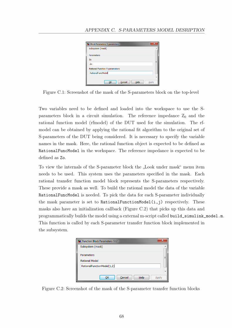
APPENDIX C. S-PARAMETERS MODEL DESRIPTION
Figure C.1: Screenshot of the mask of the S-parameters block on the top-level
Two variables need to be defined and loaded into the workspace to use the S-parameters block in a circuit simulation. The reference impedance Z0 and therational function model (rfmodel) of the DUT used for the simulation. The rf-model can be obtained by applying the rational fit algorithm to the original set ofS-parameters of the DUT being considered. It is necessary to specify the variablenames in the mask. Here, the rational function object is expected to be defined asRationalFuncModel in the workspace. The reference impedance is expected to bedefined as Zo.
To view the internals of the S-parameter block the „Look under mask“ menu itemneeds to be used. This system uses the parameters specified in the mask. Eachrational transfer function model block represents the S-parameters respectively.These provide a mask as well. To build the rational model the data of the variableRationalFuncModel is needed. To pick the data for each S-parameter individuallythe mask parameter is set to RationalFunctionModel(i,j) respectively. Thesemasks also have an initialization callback (Figure C.2) that picks up this data andprogrammatically builds the model using a external m-script called build_simulink_model.m.This function is called by each S-parameter transfer function block implemented inthe subsystem.
Figure C.2: Screenshot of the mask of the S-parameter transfer function blocks
68
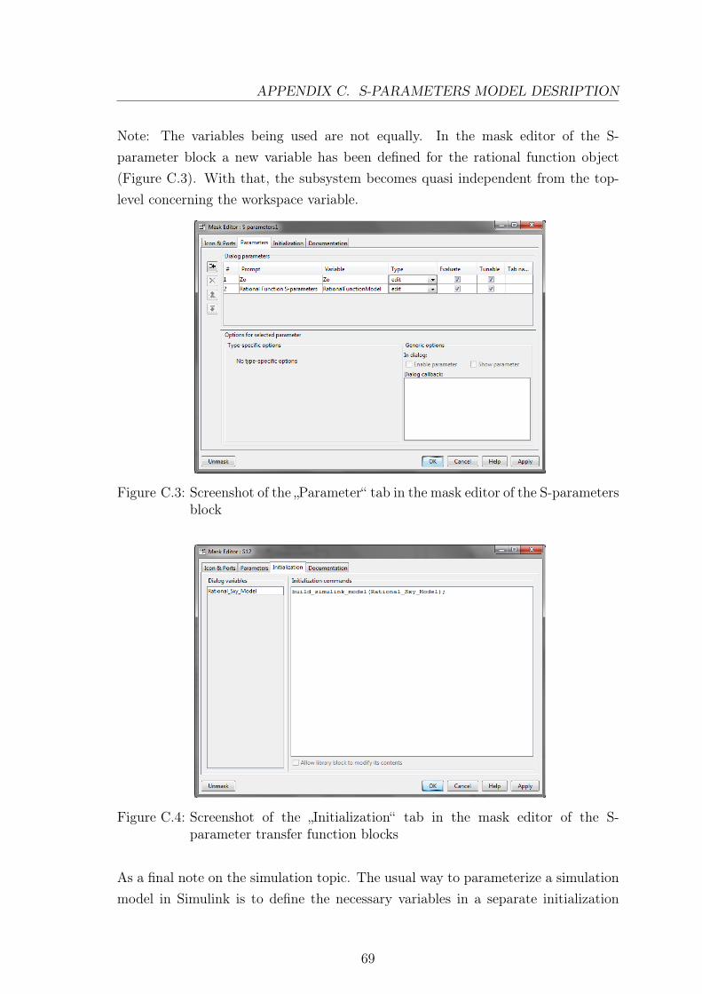
APPENDIX C. S-PARAMETERS MODEL DESRIPTION
Note: The variables being used are not equally. In the mask editor of the S-parameter block a new variable has been defined for the rational function object(Figure C.3). With that, the subsystem becomes quasi independent from the top-level concerning the workspace variable.
Figure C.3: Screenshot of the „Parameter“ tab in the mask editor of the S-parametersblock
Figure C.4: Screenshot of the „Initialization“ tab in the mask editor of the S-parameter transfer function blocks
As a final note on the simulation topic. The usual way to parameterize a simulationmodel in Simulink is to define the necessary variables in a separate initialization
69
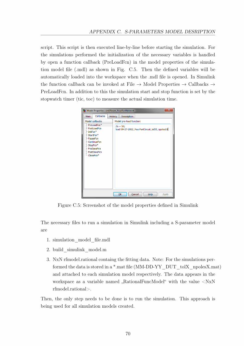
APPENDIX C. S-PARAMETERS MODEL DESRIPTION
script. This script is then executed line-by-line before starting the simulation. Forthe simulations performed the initialization of the necessary variables is handledby open a function callback (PreLoadFcn) in the model properties of the simula-tion model file (.mdl) as shown in Fig. C.5. Then the defined variables will beautomatically loaded into the workspace when the .mdl file is opened. In Simulinkthe function callback can be invoked at File → Model Properties → Callbacks →PreLoadFcn. In addition to this the simulation start and stop function is set by thestopwatch timer (tic, toc) to measure the actual simulation time.
Figure C.5: Screenshot of the model properties defined in Simulink
The necessary files to run a simulation in Simulink including a S-parameter modelare
1. simulation_model_file.mdl
2. build_simulink_model.m
3. NxN rfmodel.rational containg the fitting data. Note: For the simulations per-formed the data is stored in a *.mat file (MM-DD-YY_DUT_tolX_npolesX.mat)and attached to each simulation model respectively. The data appears in theworkspace as a variable named „RationalFuncModel“ with the value <NxNrfmodel.rational>.
Then, the only step needs to be done is to run the simulation. This approach isbeing used for all simulation models created.
70
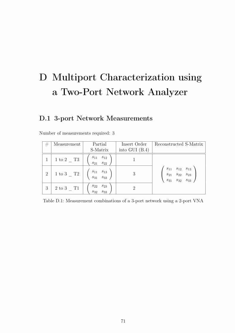
D Multiport Characterization usinga Two-Port Network Analyzer
D.1 3-port Network Measurements
Number of measurements required: 3
# Measurement PartialS-Matrix
Insert Orderinto GUI (B.4)
Reconstructed S-Matrix
1 1 to 2 _ T3(s11 s12s21 s22
)1
2 1 to 3 _ T2(s11 s13s31 s33
)3
s11 s12 s13s21 s22 s23s31 s32 s33
3 2 to 3 _ T1
(s22 s23s32 s33
)2
Table D.1: Measurement combinations of a 3-port network using a 2-port VNA
71
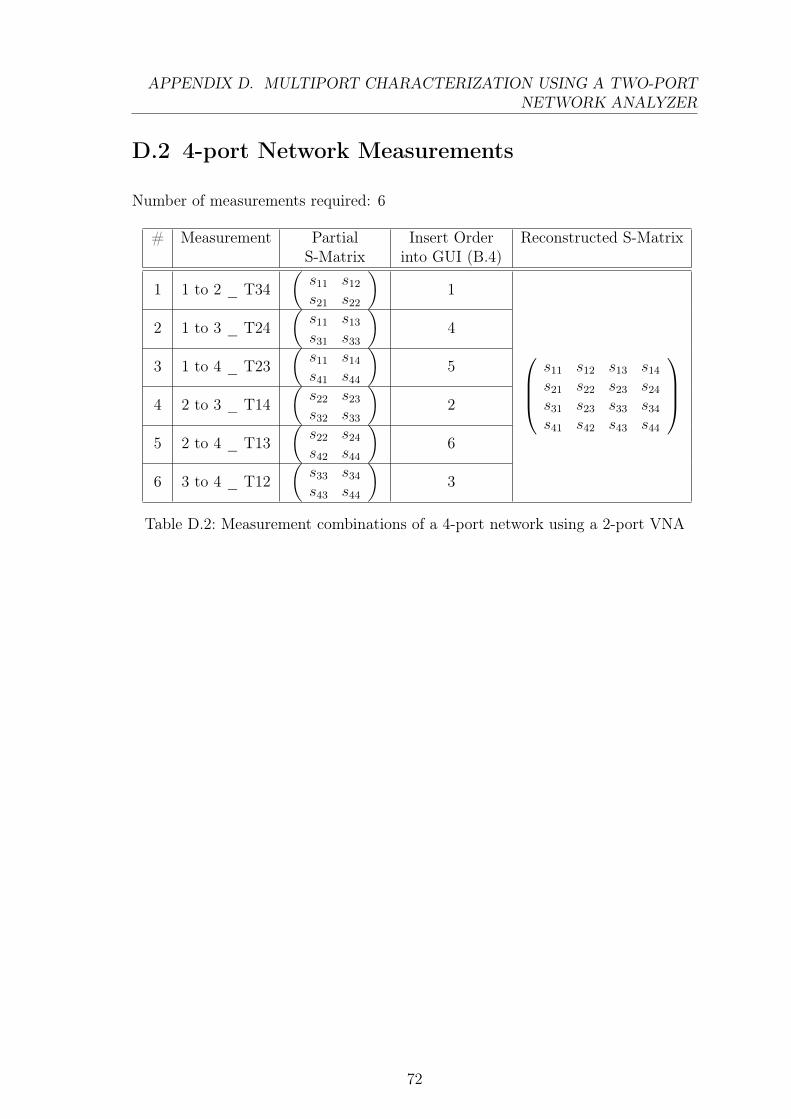
APPENDIX D. MULTIPORT CHARACTERIZATION USING A TWO-PORTNETWORK ANALYZER
D.2 4-port Network Measurements
Number of measurements required: 6
# Measurement PartialS-Matrix
Insert Orderinto GUI (B.4)
Reconstructed S-Matrix
1 1 to 2 _ T34(s11 s12s21 s22
)1
2 1 to 3 _ T24(s11 s13s31 s33
)4
3 1 to 4 _ T23(s11 s14s41 s44
)5
s11 s12 s13 s14s21 s22 s23 s24s31 s23 s33 s34s41 s42 s43 s44
4 2 to 3 _ T14(s22 s23s32 s33
)2
5 2 to 4 _ T13(s22 s24s42 s44
)6
6 3 to 4 _ T12(s33 s34s43 s44
)3
Table D.2: Measurement combinations of a 4-port network using a 2-port VNA
72
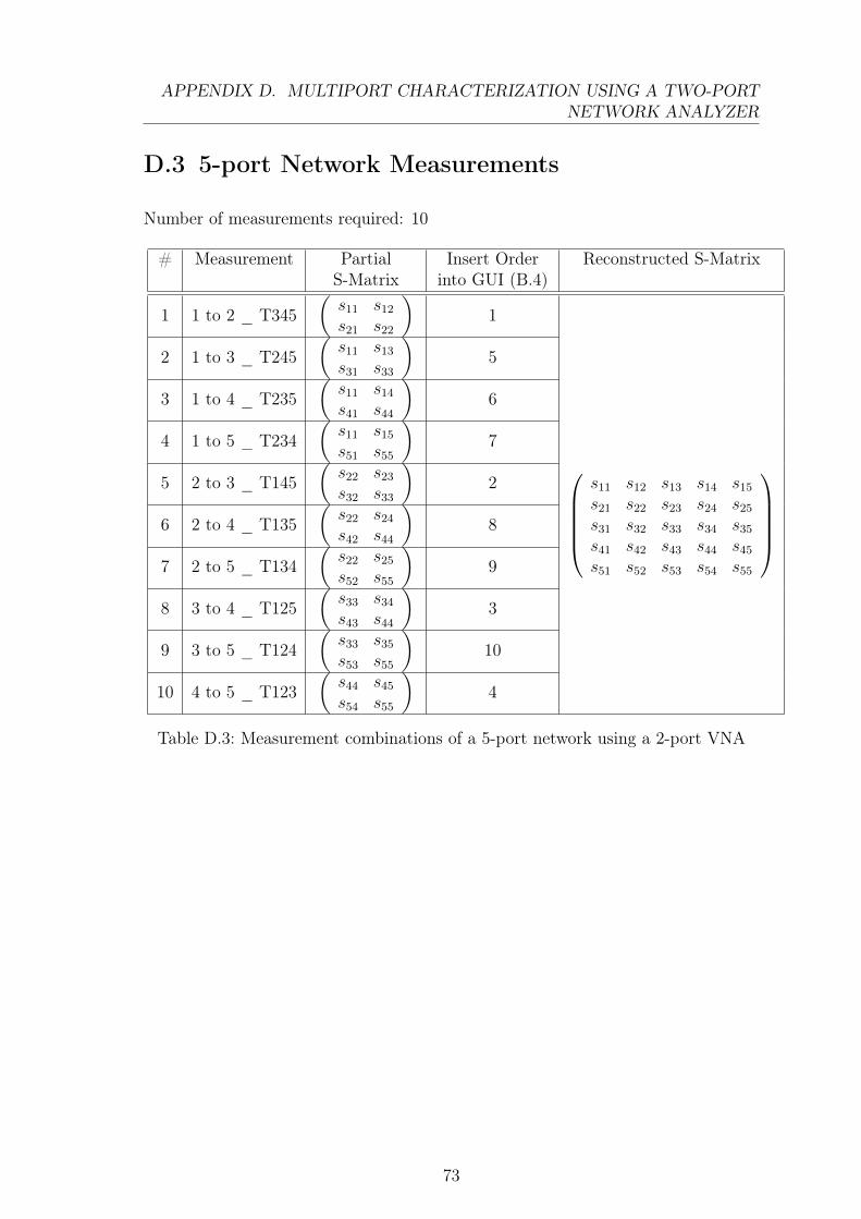
APPENDIX D. MULTIPORT CHARACTERIZATION USING A TWO-PORTNETWORK ANALYZER
D.3 5-port Network Measurements
Number of measurements required: 10
# Measurement PartialS-Matrix
Insert Orderinto GUI (B.4)
Reconstructed S-Matrix
1 1 to 2 _ T345(s11 s12s21 s22
)1
2 1 to 3 _ T245(s11 s13s31 s33
)5
3 1 to 4 _ T235(s11 s14s41 s44
)6
4 1 to 5 _ T234(s11 s15s51 s55
)7
5 2 to 3 _ T145(s22 s23s32 s33
)2
s11 s12 s13 s14 s15s21 s22 s23 s24 s25s31 s32 s33 s34 s35s41 s42 s43 s44 s45s51 s52 s53 s54 s55
6 2 to 4 _ T135(s22 s24s42 s44
)8
7 2 to 5 _ T134(s22 s25s52 s55
)9
8 3 to 4 _ T125(s33 s34s43 s44
)3
9 3 to 5 _ T124(s33 s35s53 s55
)10
10 4 to 5 _ T123(s44 s45s54 s55
)4
Table D.3: Measurement combinations of a 5-port network using a 2-port VNA
73
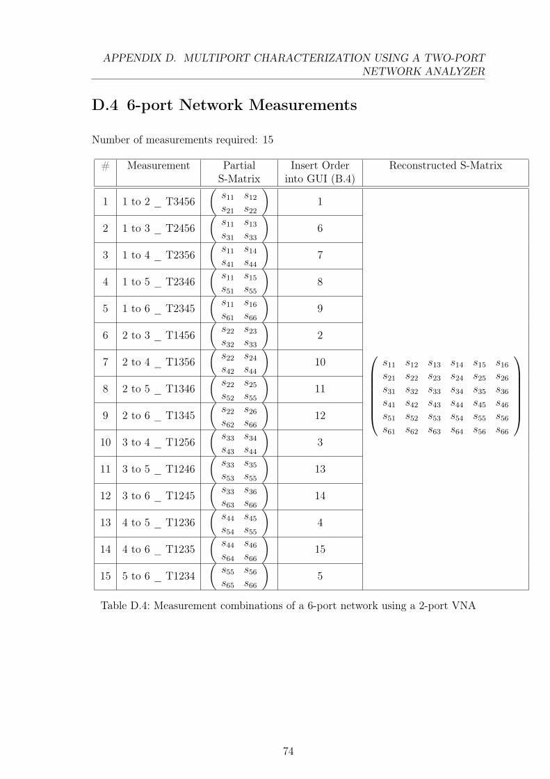
APPENDIX D. MULTIPORT CHARACTERIZATION USING A TWO-PORTNETWORK ANALYZER
D.4 6-port Network Measurements
Number of measurements required: 15
# Measurement PartialS-Matrix
Insert Orderinto GUI (B.4)
Reconstructed S-Matrix
1 1 to 2 _ T3456(s11 s12s21 s22
)1
2 1 to 3 _ T2456(s11 s13s31 s33
)6
3 1 to 4 _ T2356(s11 s14s41 s44
)7
4 1 to 5 _ T2346(s11 s15s51 s55
)8
5 1 to 6 _ T2345(s11 s16s61 s66
)9
6 2 to 3 _ T1456(s22 s23s32 s33
)2
7 2 to 4 _ T1356(s22 s24s42 s44
)10
s11 s12 s13 s14 s15 s16s21 s22 s23 s24 s25 s26s31 s32 s33 s34 s35 s36s41 s42 s43 s44 s45 s46s51 s52 s53 s54 s55 s56s61 s62 s63 s64 s56 s66
8 2 to 5 _ T1346
(s22 s25s52 s55
)11
9 2 to 6 _ T1345(s22 s26s62 s66
)12
10 3 to 4 _ T1256(s33 s34s43 s44
)3
11 3 to 5 _ T1246(s33 s35s53 s55
)13
12 3 to 6 _ T1245(s33 s36s63 s66
)14
13 4 to 5 _ T1236(s44 s45s54 s55
)4
14 4 to 6 _ T1235(s44 s46s64 s66
)15
15 5 to 6 _ T1234(s55 s56s65 s66
)5
Table D.4: Measurement combinations of a 6-port network using a 2-port VNA
74