nsfec workshop report - national science foundation · full details are provided in this report of...
TRANSCRIPT
NSF-EC WORKSHOP ON NANOMANUFACTURING AND PROCESSING
Summary Report 1. WORKSHOP OVERVIEW The NSF-EC Workshop on Nanomanufacturing and Processing was held in San Juan, Puerto Rico on 5-7 January 2002. The Workshop was held within the framework of the cooperation between the National Science Foundation (NSF) and the European Commission (EC, materials sciences), with the aim of catalyzing progress in research and education in the emerging field of Nanomanufacturing and processing. It is envisioned that this NSF-EC cooperation will provide a critical thrust to translate the growing global investments in the field of Nanoscale Science and Engineering into new scientific developments and engineering applications that will have a mutually beneficial impact for both the U.S. and European research partners and broader societies. Specific objectives of the workshop were to identify:
• research milestones that would have a catalytic effect in exploring and mastering the entire area of nanoscale processing and manufacturing, and in revolutionizing its utilization for the full spectrum of potential longer-term applications. The research milestones were organized into four thematic areas: (a) nanomaterials and nanomanufacturing; (b) prototyping, scale-up, and integration issues in nanomanufacturing; (c) measurement and metrology; and (d) theory, modeling, and simulation.
• potential implications, impacts, and applications of nanomanufacturing in the promotion of international security;
• a support plan for the infrastructure required to achieve the research/education objectives. This includes resources for support of needed developments in education and workforce training, novel ideas, and research and education facilities for knowledge creation and transfer. Furthermore, it addresses strategies for implementation of the required ethical, legal, economic and societal frameworks.
• potential collaborations between the American and European nanotechnology communities at all levels, as well as expansion of current international program initiatives and the possibility of developing new joint NSF (U.S. federal) - EC programmatic initiatives;
• methods to disseminate information and report the workshop recommendations, to cross-fertilize interactions across various disciplines, and to attract attention to the research opportunities in the nanomanufacturing/processing area.

NSF-EC Workshop on Nanomanufacturing and Processing
2
Primary Recommendations Full details are provided in this report of the structure and outcomes of the workshop. While there were many strong recommendations and specific ideas generated to move the research forward, the following three recommendations probably best capture the spirit of the discussion regarding the role of NSF and the EC in supporting the advancement of Nanomanufacturing: • Infrastructure The cross-discipinary, multi-scale nature of nanomanufacturing suggests that there will be a need for integrated/combinatorial/hybrid equipment and “next generation” fabrication laboratories to provide researchers with measurement capabilities and materials. Because of the likely cost and complexity of this equipment, a network of geographically distributed centers, with telefabrication and telecharacterization capabilities, interacting with current centers and networks (e.g., NNUN), appears to be a viable model. This will provide the crucial and presently missing link of nanomanufacturing research infrastructure, bridging current NSF investments in nanoscience (as represented by the six Nanoscale Science and Engineering Centers, NSEC), and in technology transfer to nanotechnology users (represented by the National Nanofabrication Users Network, NNUN). Such a nanomanufacturing facility network is expected to be instrumental and catalytic for progress in nanoscience and nanotechnology education, including curriculum and program development, workforce training, public information and joint academic-federal-industry programs involving demonstrative, hands-on constructivist, and international collaboration projects. • Tools
In the past, the development and broad application of instruments such as the scanning electron microscope (SEM), scanning probe microscope (SPM), and atomic force microscope (AFM) have opened up entirely new domains of knowledge – e.g., interpreting fracture, surface roughness, and adhesion at micron and submicron levels. To study features and phenomena at the nanoscale requires instruments capable of resolutions at the nano-, subnano-, and even pico-levels. The challenge in nanomanufacturing will be not only to develop new experimental and analytical tools with a broader range of capabilities at the nanoscale (e.g., chemical analysis, surface and sub-surface defects, sub-surface properties, charge transport, spectroscopy), but these tools must also work in situ, real-time, non-intrusively or destructively, and under the variable conditions seen in processing (e.g., temperature, pressure, electrical and magnetic fields). As new instruments are developed, new methods of calibration and standardization and in concert, affordable calibration standards, must be developed to ensure the accurate interpretation of results. For calibration, measurement, and assembly, reproducible positioning and repositioning with nanometer accuracy is needed. • People and Ideas One of the key barriers to rapid progress in such a cross-disciplinary field is the difficulty of building teams with the appropriate mix of expertise. Each group by itself views the problem with a narrow scope and from a specified point of view. Organizations such as the NSF and the EC can serve to facilitate the interaction between various technical and geographic groups through funding support and through coordinating meetings such as this workshop.

NSF-EC Workshop on Nanomanufacturing and Processing
3
2. NANOMANUFACTURING: DEFINITION AND PROMISE Nanomanufacturing encompasses all processes aimed toward building of nanoscale (in 1D, 2D, or 3D) structures, features, devices, and systems suitable for integration across higher dimensional scales (micro-, meso- and macroscale) to provide functional products and useful services. Nanomanufacturing includes both bottom-up and top-down processes. While clearly not comprehensive, Table 1 gives examples of a few nanomanufacturing processes.
Table 1. Examples of nanomanufacturing processes Bottom-Up Processes Top-Down Processes Contact printing, Imprinting E-beam, ion beam lithography Template growth Scanning probe lithography Spinodal wetting/dewetting Optical near field lithography Laser trapping/tweezer Femto-, atto-sec laser Assembly and joining (Self- and directed assembly)
Material removal processes (mechanical, chemical, and hybrids)
Electrostatic (coatings and fibers) Electro-erosive processes (electro, chemical, and mechanical)
Colloidal aggregation Ultrasonic material removal Figures 1 and 2 show examples of two of these processes -- a “nanotweezer” and focused ion beam lithography. With both of these methods, materials can be manipulated at the nanoscale to obtain specified positioning, size, and/or structure. The question that arises, however, is how to scale up these processes to robust, high volume, high rate production.
Figure 1. The concept of a “nanotweezer” (from Bøggild et al., Proc IEEE Nano 2001, 87)
NSF-EC Workshop on Nanomanufacturing and Processing
4
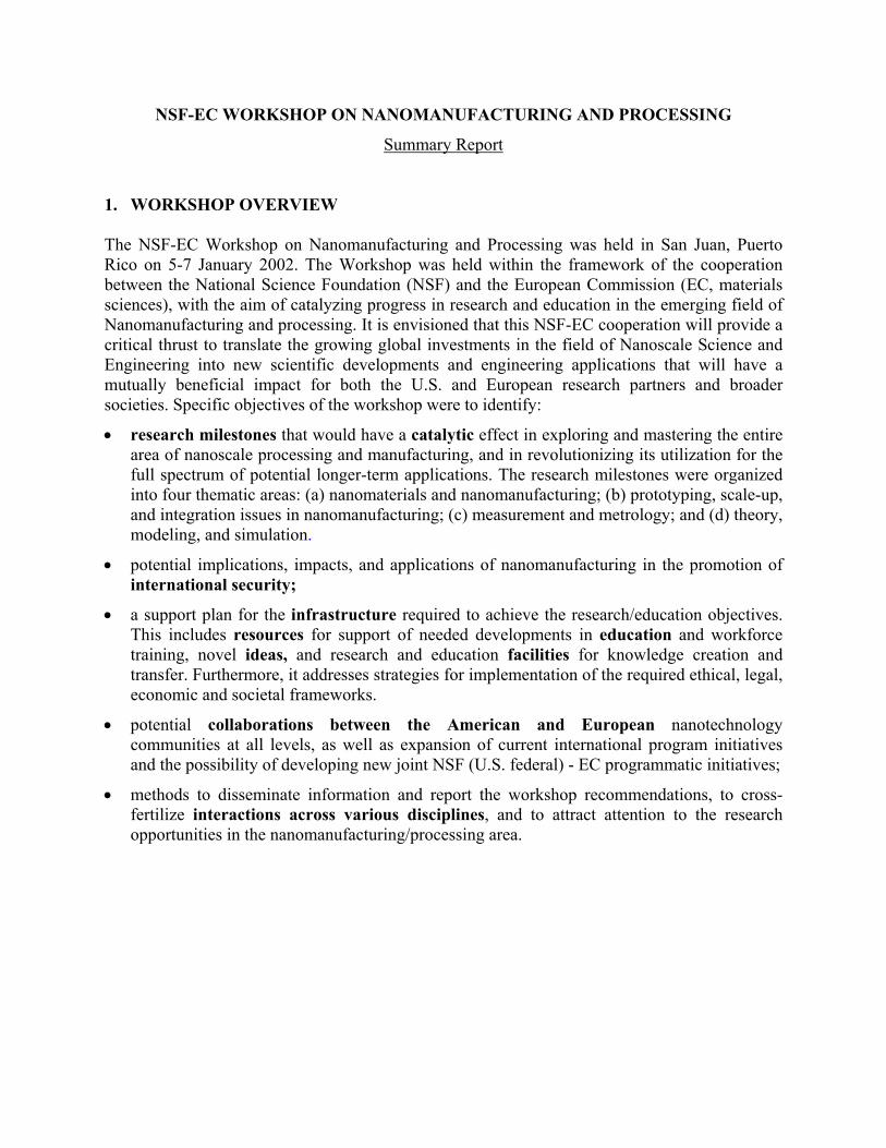
Figure 2. Focused ion beam lithography, incorporated with localized epitaxy of gallium nitride (from P. Gibart, CRHEA-CNRS Valbonne)
Nanotechnology is not only a frontier-field of science, but also the basis for a new economy. Nanomanufacturing is expected to provide new capabilities and product or service lines to traditional industries, such as automotive, aerospace, electronics, power, chemical, biomedical, and health. Furthermore, nanomanufacturing holds the exceptional promise of creating completely new markets for the nascent manufacturing industries of nanoparticles, nanostructures, and nanodevices. Advances in nanomanufacturing are anticipated to result in rapid progress in nanomaterials technology, providing enabling technologies for the advancement of information and communications technology, biotechnology and medicine, photonics/electronics technology, and security. Examples include developments in high density data storage and manipulation utilizing “nanosemiconductors,” molecular electronics, and spintronics (e.g., Fig.3). Nanoscale structures can be used in new biomaterials for prosthetic devices and medical aids. Significant improvements in diagnostics and drug delivery can be achieved through nanostructures that can more effectively target defective cells and travel within the human body (Fig.4). Similarly, because of high surface area/volume ratios, safety and security aspects such as sensors, filters, and decontaminants demonstrate increased sensitivity and yield. Finally, nanoelectromechanical (NEMS) devices and nanorobots can potentially serve as both nanomanufacturing facilitators and end-products. Of equal importance is the recognition that nanotechnology represents a whole new way of looking at technical education, cutting across traditional departmental boundaries. Current research efforts in nanomanufacturing rely on the combined expertise of scientists and engineers, including biologists, chemists, physicists, materials scientists, mechanical engineers, chemical engineers, and electrical engineers. This is expected to provide new dimensions and open new opportunities in the education business, for nurturing a new generation of nanoscience and nanoengineering researchers and teachers, and for training the nanotechnology workforce professionals. As such, new educational tools and programs will be needed to educate “nanotechnologists”, i.e., researchers and operators characterized by high multi-disciplinary skills, by capitalizing on and transforming the existing academic institutions and laboratory infrastructure. Finally, as with any new technology area, it is critical that the safety, ethical, and social impacts be studied and addressed.

NSF-EC Workshop on Nanomanufacturing and Processing
5
Figure 3. Currents passed between perpendicular nanowires alter the conductivity of organic molecules sandwiched in between (from Heath et al., Science, August 3, 2001, 239)
Figure 4. Shell-crosslinked hollow nanospheres can act as drug delivery systems or sequestrants (from McCarthy and Nicolosi, U of Massachusetts Lowell)
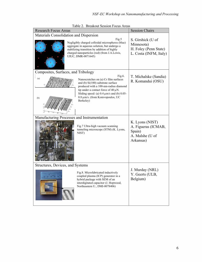
3. WORKSHOP STRUCTURE Fifty people participated in the workshop, including 34 U.S. researchers, 7 NSF Directors, 7 European researchers, and 2 EC officials. The program included several keynote talks addressing the state-of-the-art in nanoscience and technology and the status of various programs supported by NSF and the EC in this area. This was followed by several individual presentations and discussion of workshop objectives in four concurrent breakout sessions listed in Table 2, spanning the areas of expertise of the attendees. The associated figures (Figs. 4-8), although not by any means all-encompassing, help to illustrate the focus of each session. Finally, the discussion summaries from all of the sessions were combined, and recommendations were prepared [F. Biscarini (ISMN, Italy), J. Chen (U of Massachusetts Lowell), R. Komanduri (OSU), and C. Taliani (ISMN, Italy)] and presented to all of the workshop participants for further discussion. A summary of the recommendations is provided below. The recommendations were further delineated in terms of: (a) timeframe (short term: by 2005, long term: by 2010 for the research and security milestones;
short term: less than 1 year, long term: greater than 1 year for the resources, cooperation, and interaction objectives);
(b) impact (broad versus specific in both research directions, security implications, necessitated resources, NSF-EC collaborations, and community interactions); and
(c) nanomanufacturing content (i.e. the dependence of progress in research and security on nanomanufacturing issues, as well as the specificity of resources, collaborations, and interactions towards nanomanufacturing issues).
NSF-EC Workshop on Nanomanufacturing and Processing
6
Table 2. Breakout Session Focus Areas Research Focus Areas Session Chairs Materials Consolidation and Dispersion
Fig.5 Negligibly charged colloidal microspheres (blue) aggregate in aqueous solution, but undergo a stabilizing transition by addition of highly charged nanoparticles (red) (from J.A.Lewis, UIUC, DMR-0071645)
S. Girshick (U of Minnesota) H. Foley (Penn State) L. Costa (INFM, Italy)
Composites, Surfaces, and Tribology Fig.6. Nanoscratches on (a) Cr film surfaces and (b) Si(100) substrate surface produced with a 100-nm-radius diamond tip under a contact force of 40 µN. Sliding speed: (a) 0.4 µm/s and (b) 0.05-0.8 µm/s. (from Komvopoulos, UC Berkeley)
T. Michalske (Sandia) R. Komandui (OSU)
Manufacturing Processes and Instrumentation Fig.7 Ultra-high vacuum scanning tunneling microscope (STM) (K. Lyons, NIST)
K. Lyons (NIST) A. Figueras (ICMAB, Spain) A. Malshe (U of Arkansas)
Structures, Devices, and Systems Fig.8. Microfabricated inductively coupled plasma (ICP) generator in a hybrid package with SEM of an interdigitated capacitor (J. Hopwood, Northeastern U., DMI-0078406)
J. Murday (NRL) Y. Geerts (ULB, Belgium)
(b)
(a)
NSF-EC Workshop on Nanomanufacturing and Processing
7
4. RECOMMENDATIONS 4.1. Research Milestones The research milestones were organized into four thematic areas: (a) nanomaterials and nanomanufacturing; (b) prototyping, scale-up, and integration issues in nanomanufacturing; (c) measurement and metrology; and (d) theory, modeling, and simulation.
4.1.1. Nanomaterials and Nanomanufacturing
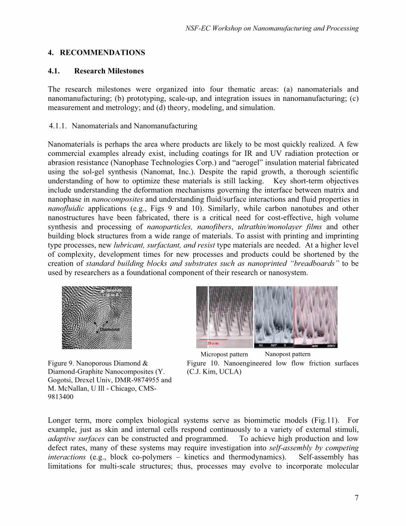
Nanomaterials is perhaps the area where products are likely to be most quickly realized. A few commercial examples already exist, including coatings for IR and UV radiation protection or abrasion resistance (Nanophase Technologies Corp.) and “aerogel” insulation material fabricated using the sol-gel synthesis (Nanomat, Inc.). Despite the rapid growth, a thorough scientific understanding of how to optimize these materials is still lacking. Key short-term objectives include understanding the deformation mechanisms governing the interface between matrix and nanophase in nanocomposites and understanding fluid/surface interactions and fluid properties in nanofluidic applications (e.g., Figs 9 and 10). Similarly, while carbon nanotubes and other nanostructures have been fabricated, there is a critical need for cost-effective, high volume synthesis and processing of nanoparticles, nanofibers, ultrathin/monolayer films and other building block structures from a wide range of materials. To assist with printing and imprinting type processes, new lubricant, surfactant, and resist type materials are needed. At a higher level of complexity, development times for new processes and products could be shortened by the creation of standard building blocks and substrates such as nanoprinted “breadboards” to be used by researchers as a foundational component of their research or nanosystem.
Figure 9. Nanoporous Diamond & Diamond-Graphite Nanocomposites (Y. Gogotsi, Drexel Univ, DMR-9874955 and M. McNallan, U Ill - Chicago, CMS-9813400
Figure 10. Nanoengineered low flow friction surfaces (C.J. Kim, UCLA)
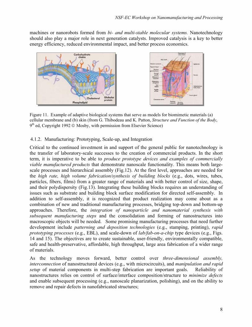
Longer term, more complex biological systems serve as biomimetic models (Fig.11). For example, just as skin and internal cells respond continuously to a variety of external stimuli, adaptive surfaces can be constructed and programmed. To achieve high production and low defect rates, many of these systems may require investigation into self-assembly by competing interactions (e.g., block co-polymers – kinetics and thermodynamics). Self-assembly has limitations for multi-scale structures; thus, processes may evolve to incorporate molecular
Micropost pattern Nanopost pattern
20 µm20 µm
NSF-EC Workshop on Nanomanufacturing and Processing
8
machines or nanorobots formed from bi- and multi-stable molecular systems. Nanotechnology should also play a major role in next generation catalysts. Improved catalysis is a key to better energy efficiency, reduced environmental impact, and better process economics.
Figure 11. Example of adaptive biological systems that serve as models for biomimetic materials (a) cellular membrane and (b) skin (from G. Thibodeau and K. Patton, Structure and Function of the Body, 9th ed, Copyright 1992 Mosby, with permission from Elsevier Science)
4.1.2. Manufacturing: Prototyping, Scale-up, and Integration
Critical to the continued investment in and support of the general public for nanotechnology is the transfer of laboratory-scale successes to the creation of commercial products. In the short term, it is imperative to be able to produce prototype devices and examples of commercially viable manufactured products that demonstrate nanoscale functionality. This means both large-scale processes and hierarchical assembly (Fig.12). At the first level, approaches are needed for the high rate, high volume fabrication/synthesis of building blocks (e.g., dots, wires, tubes, particles, fibers, films) from a greater range of materials and with better control of size, shape, and their polydispersity (Fig.13). Integrating these building blocks requires an understanding of issues such as substrate and building block surface modification for directed self-assembly. In addition to self-assembly, it is recognized that product realization may come about as a combination of new and traditional manufacturing processes, bridging top-down and bottom-up approaches. Therefore, the integration of nanoparticle and nanomaterial synthesis with subsequent manufacturing steps and the consolidation and forming of nanostructures into macroscopic objects will be needed. Some promising manufacturing processes that need further development include patterning and deposition technologies (e.g., stamping, printing), rapid prototyping processes (e.g., EBL), and scale-down of lab/fab-on-a-chip type devices (e.g., Figs. 14 and 15). The objectives are to create sustainable, user-friendly, environmentally compatible, safe and health-preservative, affordable, high throughput, large area fabrication of a wider range of materials.
As the technology moves forward, better control over three-dimensional assembly, interconnection of nanostructured devices (e.g., with microcircuits), and manipulation and rapid setup of material components in multi-step fabrication are important goals. Reliability of nanostructures relies on control of surface/interface composition/structure to minimize defects and enable subsequent processing (e.g., nanoscale planarization, polishing), and on the ability to remove and repair defects in nanofabricated structures;

NSF-EC Workshop on Nanomanufacturing and Processing
9
Figure 12. Schematic of levels of complexity for nanomanfacturing integration and assembly.
Figure 13. Electrospun fibers (a) Hollow Polycarbonate (C. Sung, R.Varma); (b) PCL-Hydroxyapatite (S.Farboodmanesh, A.Crugnola, J.Chen); (c) Polystyrene-Polybutadiene blend (N.Viriyabanthorn, J.Mead) (from U of Massachusetts Lowell)
Figure 14. Pattern Transfer (M.Tuominen, U of Massachusetts Amherst)
Figure 15. Soft lithography (Whitesides and Stroock, Physics Today, June, 2001)
Sensors
Biomedical
NEMS
Electronics
Filtration
Production rate scale-up of Building Blocks (e.g., dots, spheres, particles, fibers, wires, films)
Substrates/Breadboards
increasing complexity
(Examples of Product Realization)
Hierarchical assembly, integration with macroscopic manufacturing steps (e.g., forming, consolidation)
???
(a) (b) (c)

NSF-EC Workshop on Nanomanufacturing and Processing
10
4.1.3. Measurements and Metrology
To study features and phenomena at the nanoscale requires instruments capable of resolutions at the nano-, subnano-, and even pico-levels. Figures 16 and 17 are examples of some of the new instruments being developed for measuring thermal and mechanical properties of nanostructures. The challenge in nanomanufacturing will be not only to develop new experimental and analytical tools with a broader range of capabilities at the nanoscale (e.g., chemical analysis, surface and sub-surface defects, sub-surface properties, charge transport, spectroscopy), but these tools must also work in situ, real-time, non-intrusively or destructively, and under the variable conditions seen in processing (e.g., temperature, pressure, electrical and magnetic fields). As new instruments are developed, new methods of calibration and standardization and in concert, affordable calibration standards, must be developed to ensure the accurate interpretation of results. For calibration, measurement, and assembly, reproducible positioning and repositioning with nanometer accuracy is needed.
Figure 16. Nanocalorimeter (Roukes, CIT) Figure 17. Nanomanipulator used in the SEM to pick up,
mount, and tensile load carbon nanotubes (R.Ruoff, T.Kowalewski, J.Huettner, et al., Northwestern U., DMR-0196399)
4.1.4. Theory, Modeling, and Simulations As nanotechnology builds upon the unique properties that matter exhibits in the form of small particles or structural clusters, nanomanufacturing research resides in the space between individual atomic/molecular (e.g., quantum) theories and bulk continuum theories. Because of this, many of the existing models and assumptions are no longer valid at this scale. Experimentation will be necessary to identify the reasons for which the existing theories break down, but to move forward requires the development of new theories, models, and simulations. Fundamentally, there are the basic structure-property-processing-performance relationships that must be established for nanomaterials and nanostructures. Of particular interest to nanomanufacturing is process modeling in restricted spatial domains where boundary effects become pervasive, nanocontact mechanics, and coupled and multiscale models. These models include coupling of various spatial and time scales, as well as coupling of physical/chemical phenomena, including non-equilibrium phenomena (e.g., transport, growth). Other primary needs include developing potentials that are appropriate for nanostructure interactions, utilizing ab initio approaches to benchmark their accuracy, and exploring statistical mechanics approaches to
NSF-EC Workshop on Nanomanufacturing and Processing
11
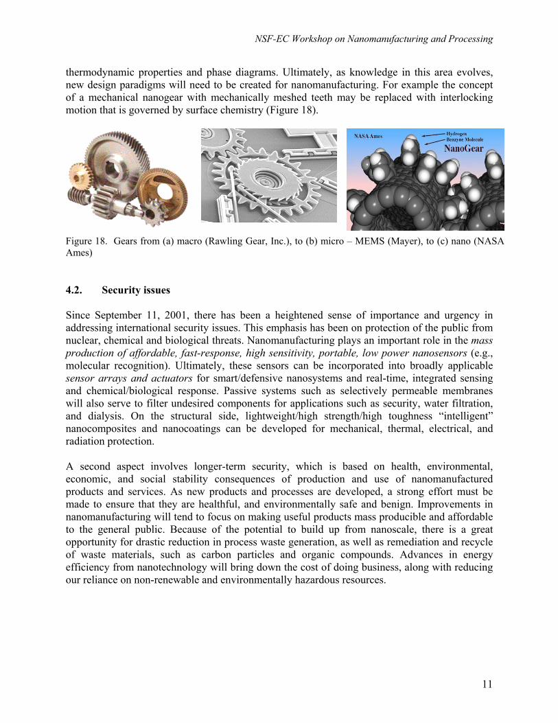
thermodynamic properties and phase diagrams. Ultimately, as knowledge in this area evolves, new design paradigms will need to be created for nanomanufacturing. For example the concept of a mechanical nanogear with mechanically meshed teeth may be replaced with interlocking motion that is governed by surface chemistry (Figure 18).
Figure 18. Gears from (a) macro (Rawling Gear, Inc.), to (b) micro – MEMS (Mayer), to (c) nano (NASA Ames)
4.2. Security issues Since September 11, 2001, there has been a heightened sense of importance and urgency in addressing international security issues. This emphasis has been on protection of the public from nuclear, chemical and biological threats. Nanomanufacturing plays an important role in the mass production of affordable, fast-response, high sensitivity, portable, low power nanosensors (e.g., molecular recognition). Ultimately, these sensors can be incorporated into broadly applicable sensor arrays and actuators for smart/defensive nanosystems and real-time, integrated sensing and chemical/biological response. Passive systems such as selectively permeable membranes will also serve to filter undesired components for applications such as security, water filtration, and dialysis. On the structural side, lightweight/high strength/high toughness “intelligent” nanocomposites and nanocoatings can be developed for mechanical, thermal, electrical, and radiation protection. A second aspect involves longer-term security, which is based on health, environmental, economic, and social stability consequences of production and use of nanomanufactured products and services. As new products and processes are developed, a strong effort must be made to ensure that they are healthful, and environmentally safe and benign. Improvements in nanomanufacturing will tend to focus on making useful products mass producible and affordable to the general public. Because of the potential to build up from nanoscale, there is a great opportunity for drastic reduction in process waste generation, as well as remediation and recycle of waste materials, such as carbon particles and organic compounds. Advances in energy efficiency from nanotechnology will bring down the cost of doing business, along with reducing our reliance on non-renewable and environmentally hazardous resources.

NSF-EC Workshop on Nanomanufacturing and Processing
12
4.3. Resources 4.3.1. Equipment
The key to achieving the research and educational objectives for nanomanufacturing in a revolutionary timeframe is the proper application of sufficient resources. Because of the change in scale and paradigm, enhanced funding to provide and develop major research equipment and new instrumentation, as well as easy access to this equipment, was deemed crucial. For example, fabrication of nanoscale products and devices may require the scaling down of machines and equipment to manipulate and assemble at sub-nanoscale accuracies. This suggests the invention of micromachining centers, microfactories, and microtesters at the level of MEMS or XYZ on a chip. Because of the rapidly occurring improvements, funds for upgrades, maintenance, and technical support of sophisticated equipment would ensure that expensive equipment is effectively utilized. In the short term, major research equipment use could be supported by low-cost access to national research facilities, a model actively employed by the European countries. In Europe, member states pay for the facilities and strongly encourage their national researchers to work with them, hoping to obtain considerable scientific output for their investment. For the longer term, the cross-discipinary, multi-scale nature of nanomanufacturing suggests that there will be a need for integrated/combinatorial/hybrid equipment and “next generation” fabrication laboratories to provide researchers with measurement capabilities and materials. Because of the likely cost and complexity of this equipment, a network of geographically distributed centers, with telefabrication and telecharacterization capabilities, interacting with current centers and networks (e.g., NNUN), appears to be a viable model. This will be integrated and provide the crucial and presently missing link of nanomanufacturing research infrastructure, bridging current NSF investments in nanoscience (as represented by the six Nanoscale Science and Engineering Centers, NSEC), and in technology transfer to nanotechnology users (represented by the National Nanofabrication Users Network, NNUN) (Figure 19). Each Nanomanufacturing Center (NMC) would specialize in certain critical areas of research needed to achieve viable manufacturing processes. For example, from the Research Milestones (Section 4.1), these focus areas could include: process monitoring instruments and control; defect detection, minimization, and removal; integration of scales; handling and positioning of nanoscale structures. To promote rapid progress, the NMCs would interact with and build upon the ongoing research at the NSECs on surface modification, directed self-assembly, patterning techniques. NMC instrument and equipment development would focus on in-situ measurements, process controls, and tooling. The NMCs would serve as a resource to educate and collaborate with existing and emerging companies on cost-effective and novel nanomanufacturing approaches. Such a nanomanufacturing facility network is expected to be instrumental and catalytic for progress in nanoscience and nanotechnology education, including curriculum and program development, workforce training, public information and joint academic-federal-industry programs involving demonstrative, hands-on constructivist, and international collaboration projects. Another alternative is the European model of virtual centers, comprised of networks of existing research centers (e.g., multiple universities and companies) that must work together to obtain funding.

NSF-EC Workshop on Nanomanufacturing and Processing
13
NSEC NSEC NSEC Fundamental research leading to the understanding of new phenomena in the laboratory
Nanomfg Centers
Nanomfg Centers
Fundamental research addressing issues of integration, reliability, and high production rates
NNUN
Established and New Industries NNUN Access to prototyping
facilities and expertise
Figure 19. Nanomanufacturing Centers address the fundamental research needed to move discoveries from the laboratory to commercial production -- integrating with both the Nanoscale Science and Engineering Centers (NSEC) and the National Nanofabrication Users Network (NNUN).
4.3.2. Human Resources Because of the recent emergence of nanotechnology, it is important to bring more researchers into what is a very cross-disciplinary field. This applies to all levels from faculty to graduate students to undergraduates to K-12 (i.e., ages 5-18). To achieve this, programs that foster mentoring of both young and mid-career faculty are recommended (Figure 20). Graduate students can be supported through dedicated graduate fellowships and interdisciplinary graduate programs in Nanotechnology. In recognition of the interdisciplinary nature, it is recognized that release time for development of new educational materials and tools (e.g., textbooks, audiovisual/multimedia material, websites, monographs) is needed. Part of this endeavor involves the identification of basic skill sets that will enable undergraduate and graduate students to tackle interdisciplinary problems. Ultimately, it is anticipated that researchers must learn a new type of interdisciplinary “subject” language, promote interdisciplinary skills, and continue to grow the knowledge base with the subject. To educate the next generation, support for K-12 educational efforts should be provided. Finally, any funds dedicated to equipment should consider the support of technicians to operate these machines for 3-5 years. All of these activities can be integrated within the nanomanufacturing network, ensuring strong ties to research activity and practical examples of exciting products and processes.
Undergraduate and graduate fellowships
Mentoring of early and mid-career faculty
Nanomanufacturing: Human resources – Continuing Education
K-12 education (students & teachers) Technician support
New educational tools; new cross-disciplinary “basic” skill set
Figure 20. Education and training needs
NSF-EC Workshop on Nanomanufacturing and Processing
14
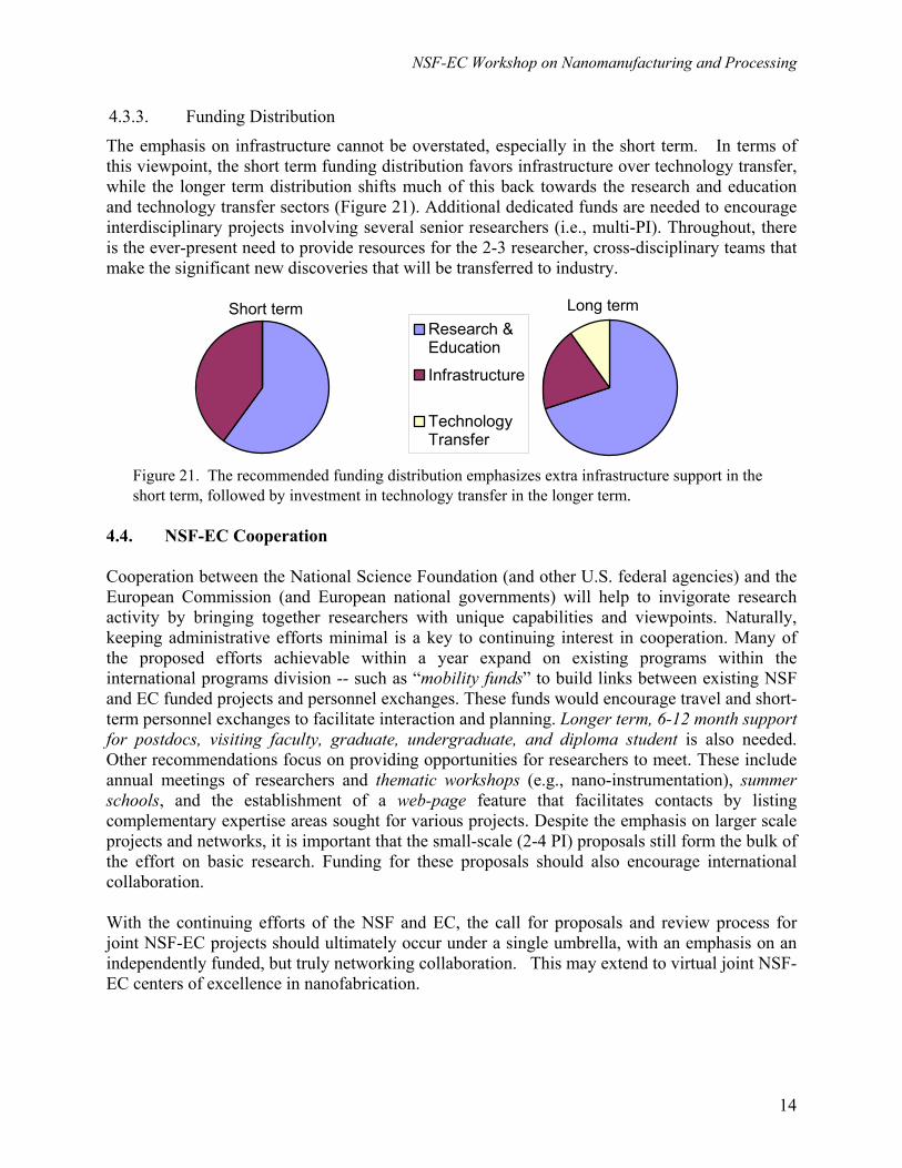
4.3.3. Funding Distribution
The emphasis on infrastructure cannot be overstated, especially in the short term. In terms of this viewpoint, the short term funding distribution favors infrastructure over technology transfer, while the longer term distribution shifts much of this back towards the research and education and technology transfer sectors (Figure 21). Additional dedicated funds are needed to encourage interdisciplinary projects involving several senior researchers (i.e., multi-PI). Throughout, there is the ever-present need to provide resources for the 2-3 researcher, cross-disciplinary teams that make the significant new discoveries that will be transferred to industry.
Short term Long termResearch &Education
Infrastructure
TechnologyTransfer
Figure 21. The recommended funding distribution emphasizes extra infrastructure support in the short term, followed by investment in technology transfer in the longer term.
4.4. NSF-EC Cooperation
Cooperation between the National Science Foundation (and other U.S. federal agencies) and the European Commission (and European national governments) will help to invigorate research activity by bringing together researchers with unique capabilities and viewpoints. Naturally, keeping administrative efforts minimal is a key to continuing interest in cooperation. Many of the proposed efforts achievable within a year expand on existing programs within the international programs division -- such as “mobility funds” to build links between existing NSF and EC funded projects and personnel exchanges. These funds would encourage travel and short-term personnel exchanges to facilitate interaction and planning. Longer term, 6-12 month support for postdocs, visiting faculty, graduate, undergraduate, and diploma student is also needed. Other recommendations focus on providing opportunities for researchers to meet. These include annual meetings of researchers and thematic workshops (e.g., nano-instrumentation), summer schools, and the establishment of a web-page feature that facilitates contacts by listing complementary expertise areas sought for various projects. Despite the emphasis on larger scale projects and networks, it is important that the small-scale (2-4 PI) proposals still form the bulk of the effort on basic research. Funding for these proposals should also encourage international collaboration. With the continuing efforts of the NSF and EC, the call for proposals and review process for joint NSF-EC projects should ultimately occur under a single umbrella, with an emphasis on an independently funded, but truly networking collaboration. This may extend to virtual joint NSF-EC centers of excellence in nanofabrication.
NSF-EC Workshop on Nanomanufacturing and Processing
15
4.5. Interactions with the Community At-large. Critical to the ultimate success of the nanomanufacturing effort is being able to inform the general public about the promise of nanomanufacturing with respect to new products and services, and opportunities in education, research, and professional work. Dissemination of information to the general public must be done in a form that is exciting and understandable, utilizing widely distributed media such as popular magazines, newspapers, and TV. On a somewhat more narrow scope, informing the broader technical community of nanomanufacturing challenges and successes should be done via special symposia at major technical meetings, joint meetings, and the establishment of a pool of distinguished speakers to present to communities not currently active in nanotechnology. These efforts will help to cross-fertilize interactions across various disciplines, and stimulate nanomanufacturing research and education involvement of scholarly and professional societies from traditional disciplinary fields. 5. CONTACT INFORMATION Respectfully submitted by Fabio Biscarini (ISMN, Bologna, Italy), Julie Chen (U Massachusetts, Lowell, MA), Ranga Komanduri (OSU, Stillwater, OK), and Carlo Taliani (ISMN, Bologna, Italy). For further details contact: Dr. Haris Doumanidis, NSF Nanomanufacturing Program, Tel (703) 292-7088; Fax: (703) 292-9056; and e-mail: [email protected] (U.S. inquiries) and Dr. Renzo Tomellini, European Commission (EC) Tel: 32 2 296 36 01; and e-mail: [email protected] (European inquiries).