nt3h2111/nt3h2211 ntag i2c plus, nfc forum …energy harvesting from nfc field, so as to power...
TRANSCRIPT
1. General description
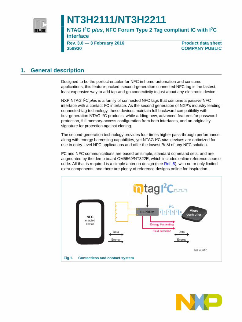
Designed to be the perfect enabler for NFC in home-automation and consumer applications, this feature-packed, second-generation connected NFC tag is the fastest, least expensive way to add tap-and-go connectivity to just about any electronic device.
NXP NTAG I2C plus is a family of connected NFC tags that combine a passive NFC interface with a contact I²C interface. As the second generation of NXP’s industry leading connected-tag technology, these devices maintain full backward compatibility with first-generation NTAG I²C products, while adding new, advanced features for password protection, full memory-access configuration from both interfaces, and an originality signature for protection against cloning.
The second-generation technology provides four times higher pass-through performance, along with energy harvesting capabilities, yet NTAG I2C plus devices are optimized for use in entry-level NFC applications and offer the lowest BoM of any NFC solution.
I²C and NFC communications are based on simple, standard command sets, and are augmented by the demo board OM5569/NT322E, which includes online reference source code. All that is required is a simple antenna design (see Ref. 5), with no or only limited extra components, and there are plenty of reference designs online for inspiration.
NT3H2111/NT3H2211NTAG I2C plus, NFC Forum Type 2 Tag compliant IC with I2C interfaceRev. 3.0 — 3 February 2016359930
Product data sheetCOMPANY PUBLIC
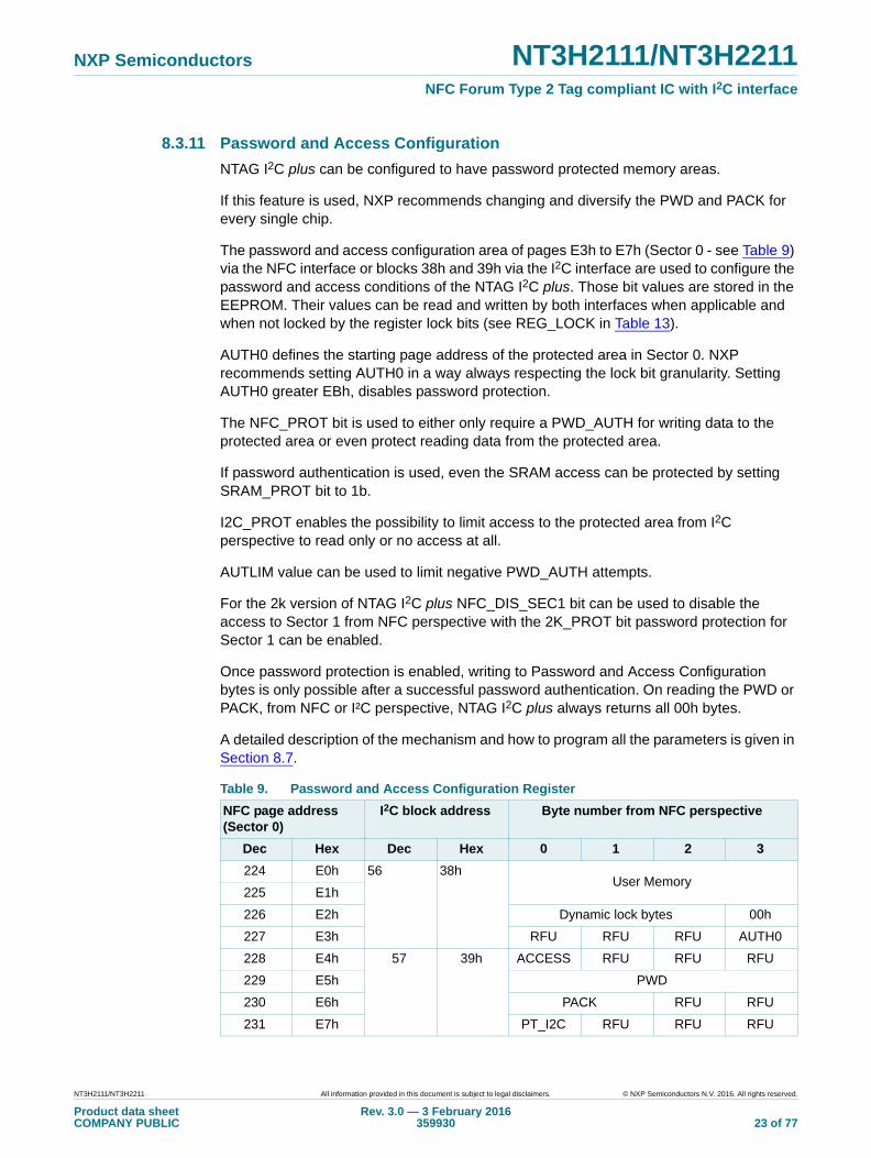
Fig 1. Contactless and contact system
aaa-010357
NFCenableddevice
Data
Energy
Data
Energy
I2C11 11 1100 00 00EEPROM
Energy Harvesting
Field detection
Microcontroller
NXP Semiconductors NT3H2111/NT3H2211NFC Forum Type 2 Tag compliant IC with I2C interface
2. Features and benefits
2.1 Key features
Interoperability
ISO/IEC 14443 Part 2 and 3 compliant
NFC Forum Type 2 Tag compliant
Unique 7-byte UID
GET_VERSION command for easy identification of chip type and supported features
Input capacitance of 50 pF
Host interface
I²C slave
Configurable event detection pin to signal NFC or pass-through data events
Memory
888/1912 bytes of EEPROM-based user memory
64 bytes SRAM buffer for transfer of data between NFC and I²C interfaces with memory mirror or pass-through mode
Clear arbitration between NFC and I²C memory access
Data transfer
Pass-through mode with 64-byte SRAM buffer
FAST_WRITE and FAST_READ NFC commands for higher data throughput
Security and memory-access management
Full, read-only, or no memory access from NFC interface, based on 32-bit password
Full, read-only, or no memory access from I²C interface
NFC silence feature to disable the NFC interface
Originality signature based on Elliptic Curve Cryptography (ECC) for simple, genuine authentication
Power Management
Configurable field-detection output signal for data-transfer synchronization and device wake-up
Energy harvesting from NFC field, so as to power external devices (e.g. connected microcontroller)
Industrial requirements
Temperature range from -40 °C up to 105 °C
2.2 NFC interface
Contactless transmission of data
NFC Forum Type 2 Tag compliant (see Ref. 1)
ISO/IEC 14443A compliant (see Ref. 2)
4 bytes (one page) written including all overhead in 4.8 ms via EEPROM or 0.8 ms via SRAM
64 bytes (whole SRAM) written including all overhead in 6.1 ms using FAST_WRITE command
NT3H2111/NT3H2211 All information provided in this document is subject to legal disclaimers. © NXP Semiconductors N.V. 2016. All rights reserved.
Product data sheetCOMPANY PUBLIC
Rev. 3.0 — 3 February 2016359930 2 of 77
NXP Semiconductors NT3H2111/NT3H2211NFC Forum Type 2 Tag compliant IC with I2C interface
Data integrity of 16-bit CRC, parity, bit coding, bit counting
Operating distance of up to 100 mm (depending on various parameters, such as field strength and antenna geometry)
True anticollision
Unique 7 byte serial number (cascade level 2 according to ISO/IEC 14443-3 (see Ref. 2)
2.3 Memory
1912 bytes freely available with User Read/Write area (478 pages with 4 bytes per pages) for the 2k version
888 bytes freely available with User Read/Write area (222 pages with 4 bytes per pages) for the 1k version
64 bytes SRAM volatile memory without write endurance limitation
Data retention time of minimum 20 years
EEPROM write endurance minimum 500.000 cycles
2.4 I²C interface
I²C slave interface supports frequencies up to 400 kHz (see Section 13.1)
16 bytes (one block) written in 4.5 ms (EEPROM) or 0.4 ms (SRAM - pass-through mode) including all overhead
RFID chip can be used as standard I2C EEPROM and I²C SRAM
2.5 Security
Manufacturer-programmed 7-byte UID for each device
Capability container with one time programmable bits
Field programmable read-only locking function per page for first 12 pages and per 16 (1k version) or 32 (2k version) pages for the extended memory section
ECC-based originality signature
32-bit password protection to prevent unauthorized memory operations from NFC perspective may be enabled for parts of, or complete memory
Access to protected data from I²C perspective may be restricted
Pass-through and mirror mode operation may be password protected
Protected data can be safeguarded against limited number of negative password authentication attempts
2.6 Key benefits
Full interoperability with every NFC-enabled device
Smooth end-user experience with super-fast data exchange via NFC and I²C interface
Zero-power operation with non-volatile data storage
Lowest bill of materials and smallest footprint for NFC solution in embedded electronics
Data protection to prevent unauthorized data manipulation
Multi-application support, enabled by memory size and segmentation options
NT3H2111/NT3H2211 All information provided in this document is subject to legal disclaimers. © NXP Semiconductors N.V. 2016. All rights reserved.
Product data sheetCOMPANY PUBLIC
Rev. 3.0 — 3 February 2016359930 3 of 77
NXP Semiconductors NT3H2111/NT3H2211NFC Forum Type 2 Tag compliant IC with I2C interface
3. Applications
NXP NTAG I2C plus is a family of connected NFC tags that combine a passive NFC interface with a contact I²C interface. As the second generation of NXP’s industry-leading connected-tag technology, these devices maintain full backward compatibility with first-generation NTAG I²C products, while adding new, advanced features for password protection, full memory-access configuration from both interfaces, and an originality signature for protection against cloning.
The second-generation technology provides four times higher pass-through performance, along with energy harvesting capabilities, yet NTAG I2C plus devices are optimized for use in entry-level NFC applications like:
IoT nodes (home automation, smart home, etc.)
Pairing and configuration of consumer applications
NFC accessories (headsets, speakers, etc.)
Wearable infotainment
Fitness equipment
Consumer electronics
Healthcare
Smart printers
Meters
Electronic shelf labels
NT3H2111/NT3H2211 All information provided in this document is subject to legal disclaimers. © NXP Semiconductors N.V. 2016. All rights reserved.
Product data sheetCOMPANY PUBLIC
Rev. 3.0 — 3 February 2016359930 4 of 77
NXP Semiconductors NT3H2111/NT3H2211NFC Forum Type 2 Tag compliant IC with I2C interface
4. Ordering information
5. Marking
Table 1. Ordering information
Type number Package
Name Description Version
NT3H2111W0FHK XQFN8 Plastic, extremely thin quad flat package; no leads; 8 terminals; body 1.6 x 1.6 x 0.6 mm; 1k bytes memory, 50pF input capacitance
SOT902-3
NT3H2211W0FHK XQFN8 Plastic, extremely thin quad flat package; no leads; 8 terminals; body 1.6 x 1.6 x 0.6 mm; 2k bytes memory, 50pF input capacitance
SOT902-3
NT3H2111W0FTT TSSOP8 Plastic thin shrink small outline package; 8 leads; body width 3 mm; 1k bytes memory; 50pF input capacitance
SOT505-1
NT3H2211W0FTT TSSOP8 Plastic thin shrink small outline package; 8 leads; body width 3 mm; 2k bytes memory; 50pF input capacitance
SOT505-1
NT3H2111W0FT1 SO8 Plastic small outline package; 8 leads; body width 3.9 mm, 1k bytes memory; 50pF input capacitance
SOT96-1
NT3H2211W0FT1 SO8 Plastic small outline package; 8 leads; body width 3.9 mm, 2k bytes memory; 50pF input capacitance
SOT96-1
NT3H2111W0FUG FFC bumped
8 inch wafer, 150um thickness, on film frame carrier, electronic fail die
marking according to SECS-II format), Au bumps, 1k Bytes memory, 50pF input capacitance
-
NT3H2211W0FUG FFC bumped
8 inch wafer, 150um thickness, on film frame carrier, electronic fail die
marking according to SECS-II format), Au bumps, 2k Bytes memory, 50pF input capacitance
-
Table 2. Marking codes
Type numberMarking code
Line 1 Line 2 Line 3
NT3H2111FHK 211 - -
NT3H2211FHK 221 - -
NT3H2111W0FTT 32111 DBSN ASID yww
NT3H2211W0FTT 32211 DBSN ASID yww
NT3H2111W0FT1 NT32111 DBSN ASID nDyww
NT3H2211W0FT1 NT32211 DBSN ASID nDyww
NT3H2111/NT3H2211 All information provided in this document is subject to legal disclaimers. © NXP Semiconductors N.V. 2016. All rights reserved.
Product data sheetCOMPANY PUBLIC
Rev. 3.0 — 3 February 2016359930 5 of 77
NXP Semiconductors NT3H2111/NT3H2211NFC Forum Type 2 Tag compliant IC with I2C interface
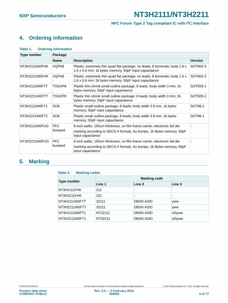
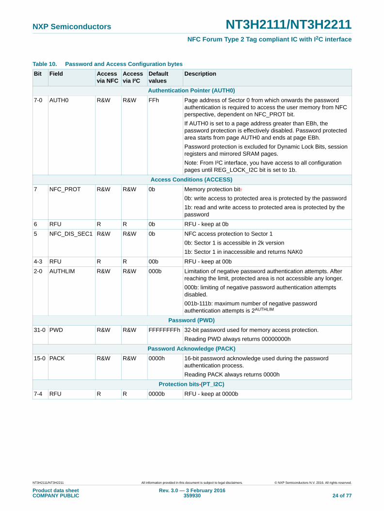
6. Block diagram
7. Pinning information
7.1 Pinning
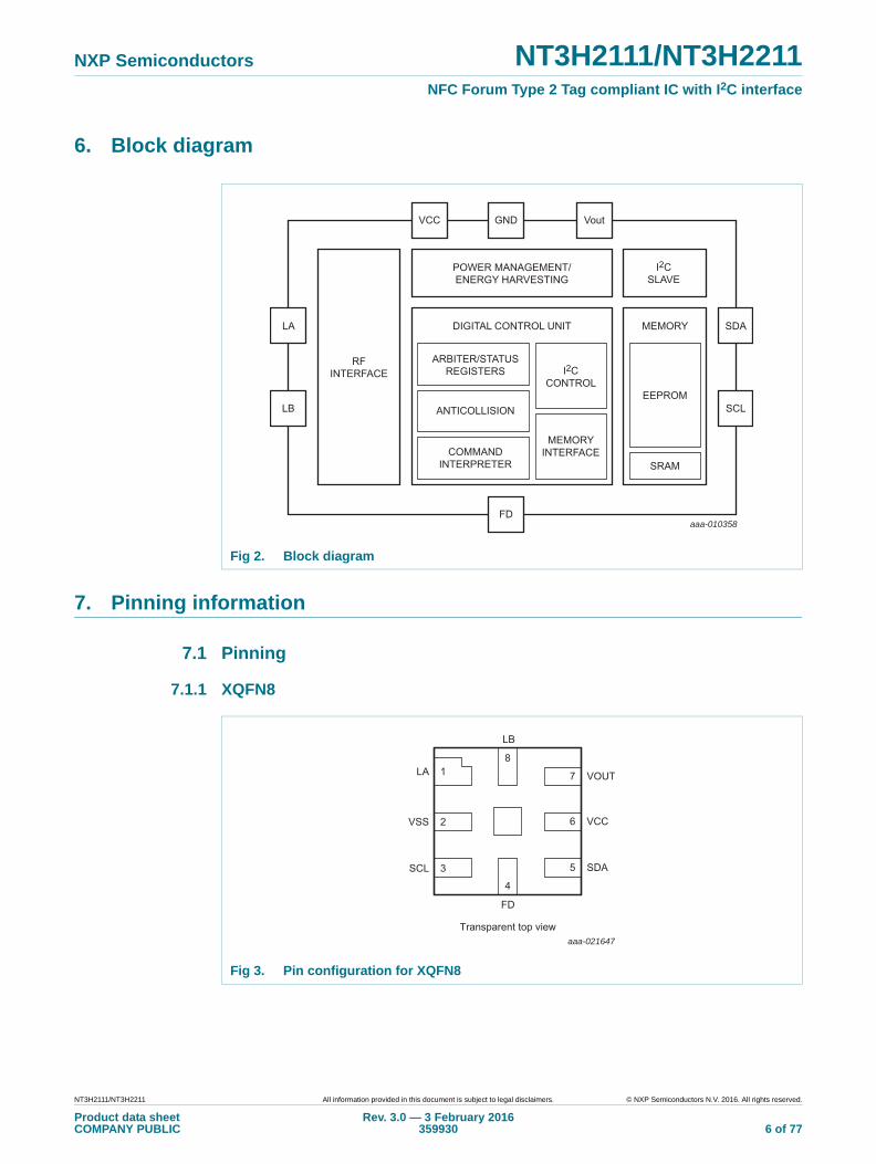
7.1.1 XQFN8
Fig 2. Block diagram
aaa-010358
I2CSLAVE
I2CCONTROL
RFINTERFACE
LA
LB
POWER MANAGEMENT/ENERGY HARVESTING
DIGITAL CONTROL UNIT MEMORY
EEPROM
SRAM
ARBITER/STATUSREGISTERS
ANTICOLLISION
COMMANDINTERPRETER
MEMORYINTERFACE
SDA
SCL
GND
FD
VoutVCC
Fig 3. Pin configuration for XQFN8
aaa-021647
FD
Transparent top view
4
8
6
5
7
3
1
2VSS
LA
SCL
LB
VCC
SDA
VOUT
NT3H2111/NT3H2211 All information provided in this document is subject to legal disclaimers. © NXP Semiconductors N.V. 2016. All rights reserved.
Product data sheetCOMPANY PUBLIC
Rev. 3.0 — 3 February 2016359930 6 of 77
NXP Semiconductors NT3H2111/NT3H2211NFC Forum Type 2 Tag compliant IC with I2C interface
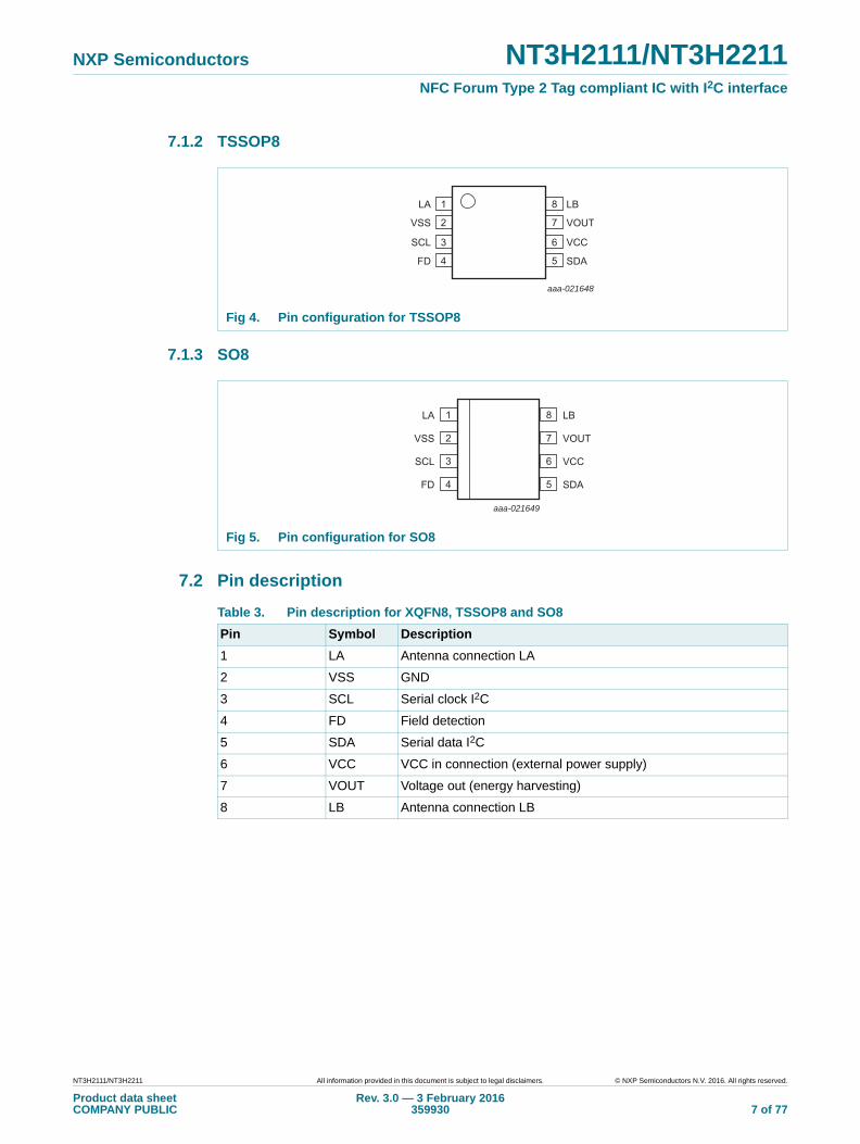
7.1.2 TSSOP8
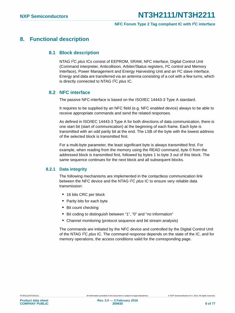
7.1.3 SO8
7.2 Pin description
Fig 4. Pin configuration for TSSOP8
aaa-021648
SDA
VCC
VOUT
LB
FD
SCL
VSS
LA 1
2
3
4
6
5
8
7
Fig 5. Pin configuration for SO8
LA LB
VSS VOUT
SCL VCC
FD SDA
aaa-021649
1
2
3
4
6
5
8
7
Table 3. Pin description for XQFN8, TSSOP8 and SO8
Pin Symbol Description
1 LA Antenna connection LA
2 VSS GND
3 SCL Serial clock I2C
4 FD Field detection
5 SDA Serial data I2C
6 VCC VCC in connection (external power supply)
7 VOUT Voltage out (energy harvesting)
8 LB Antenna connection LB
NT3H2111/NT3H2211 All information provided in this document is subject to legal disclaimers. © NXP Semiconductors N.V. 2016. All rights reserved.
Product data sheetCOMPANY PUBLIC
Rev. 3.0 — 3 February 2016359930 7 of 77
NXP Semiconductors NT3H2111/NT3H2211NFC Forum Type 2 Tag compliant IC with I2C interface
8. Functional description
8.1 Block description
NTAG I2C plus ICs consist of EEPROM, SRAM, NFC interface, Digital Control Unit (Command interpreter, Anticollision, Arbiter/Status registers, I²C control and Memory Interface), Power Management and Energy Harvesting Unit and an I²C slave interface. Energy and data are transferred via an antenna consisting of a coil with a few turns, which is directly connected to NTAG I2C plus IC.
8.2 NFC interface
The passive NFC-interface is based on the ISO/IEC 14443-3 Type A standard.
It requires to be supplied by an NFC field (e.g. NFC enabled device) always to be able to receive appropriate commands and send the related responses.
As defined in ISO/IEC 14443-3 Type A for both directions of data communication, there is one start bit (start of communication) at the beginning of each frame. Each byte is transmitted with an odd parity bit at the end. The LSB of the byte with the lowest address of the selected block is transmitted first.
For a multi-byte parameter, the least significant byte is always transmitted first. For example, when reading from the memory using the READ command, byte 0 from the addressed block is transmitted first, followed by bytes 1 to byte 3 out of this block. The same sequence continues for the next block and all subsequent blocks.
8.2.1 Data integrity
The following mechanisms are implemented in the contactless communication link between the NFC device and the NTAG I2C plus IC to ensure very reliable data transmission:
• 16 bits CRC per block
• Parity bits for each byte
• Bit count checking
• Bit coding to distinguish between “1”, “0” and “no information”
• Channel monitoring (protocol sequence and bit stream analysis)
The commands are initiated by the NFC device and controlled by the Digital Control Unit of the NTAG I2C plus IC. The command response depends on the state of the IC, and for memory operations, the access conditions valid for the corresponding page.
NT3H2111/NT3H2211 All information provided in this document is subject to legal disclaimers. © NXP Semiconductors N.V. 2016. All rights reserved.
Product data sheetCOMPANY PUBLIC
Rev. 3.0 — 3 February 2016359930 8 of 77
NXP Semiconductors NT3H2111/NT3H2211NFC Forum Type 2 Tag compliant IC with I2C interface
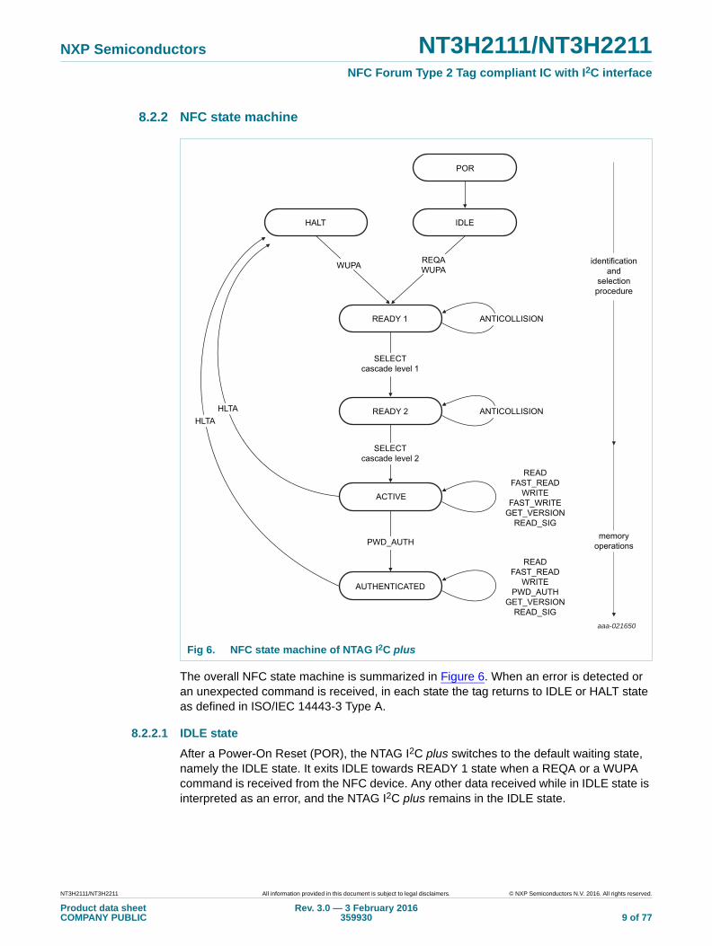
8.2.2 NFC state machine
The overall NFC state machine is summarized in Figure 6. When an error is detected or an unexpected command is received, in each state the tag returns to IDLE or HALT state as defined in ISO/IEC 14443-3 Type A.
8.2.2.1 IDLE state
After a Power-On Reset (POR), the NTAG I2C plus switches to the default waiting state, namely the IDLE state. It exits IDLE towards READY 1 state when a REQA or a WUPA command is received from the NFC device. Any other data received while in IDLE state is interpreted as an error, and the NTAG I2C plus remains in the IDLE state.
Fig 6. NFC state machine of NTAG I2C plus
PWD_AUTH
SELECTcascade level 2
SELECTcascade level 1
WUPA REQAWUPA
READY 1
READY 2
ACTIVE
AUTHENTICATED
IDLEHALT
POR
ANTICOLLISION
HLTAHLTA
memoryoperations
identificationand
selectionprocedure
aaa-021650
READFAST_READ
WRITEFAST_WRITE
GET_VERSIONREAD_SIG
ANTICOLLISION
READFAST_READ
WRITEPWD_AUTH
GET_VERSIONREAD_SIG
NT3H2111/NT3H2211 All information provided in this document is subject to legal disclaimers. © NXP Semiconductors N.V. 2016. All rights reserved.
Product data sheetCOMPANY PUBLIC
Rev. 3.0 — 3 February 2016359930 9 of 77

NXP Semiconductors NT3H2111/NT3H2211NFC Forum Type 2 Tag compliant IC with I2C interface
8.2.2.2 READY 1 state
In the READY 1 state, the NFC device resolves the first part of the UID (3 bytes) using the ANTICOLLISION or SELECT commands for cascade level 1. READY 1 state is correctly exited after execution of the following command:
• SELECT command from cascade level 1 with the matching complete first part of the UID: the NFC device switches the NTAG I2C plus into READY 2 state where the second part of the UID is resolved.
8.2.2.3 READY 2 state
In the READY 2 state, the NFC device resolves the second part of the UID (4 bytes) using the ANTICOLLISION or SELECT command for cascade level 2. READY2 state is correctly exited after execution of the following command:
• SELECT command from cascade level 2 with the matching complete second part of the UID: the NFC device switches the NTAG I2C plus into ACTIVE state where all application-related commands can be executed.
Remark: The response of the NTAG I2C plus to the SELECT command is the Select AcKnowledge (SAK) byte. In accordance with ISO/IEC 14443-3 Type A, this byte indicates if the anticollision cascade procedure has finished. If finished, the NTAG I2C plus is now uniquely selected and only this device will communicate with the NFC device even when other contactless devices are present in the NFC device field.
8.2.2.4 ACTIVE state
All unprotected memory operations are operated in the ACTIVE and AUTHENTICATED states.
The ACTIVE state is exited with the PWD_AUTH command and upon reception of a correct password, the NTAG I2C plus transits to AUTHENTICATED state after responding with PACK or with the HLTA command the NTAG I2C plus transits to the HALT state.
Any other data received when the device is in ACTIVE state is interpreted as an error. Depending on its previous state, the NTAG I2C plus returns to either to the IDLE or HALT state.
8.2.2.5 AUTHENTICATED state
Protected memory operations are only operated in the AUTHENTICATED state, however access to the unprotected memory is possible, too.
The AUTHENTICATED state is exited with the HLTA command and upon reception, the NTAG I2C plus transits to the HALT state. Any other data received when the device is in AUTHENTICATED state is interpreted as an error. Depending on its previous state, the NTAG I2C plus returns to either to the IDLE or HALT state.
8.2.2.6 HALT state
HALT and IDLE states constitute the two waiting states implemented in the NTAG I2C plus. An already processed NTAG I2C plus in ACTIVE or AUTHENTICATED state can be set into the HALT state using the HLTA command. In the anticollision phase, this state helps the NFC device distinguish between processed tags and tags yet to be selected.
NT3H2111/NT3H2211 All information provided in this document is subject to legal disclaimers. © NXP Semiconductors N.V. 2016. All rights reserved.
Product data sheetCOMPANY PUBLIC
Rev. 3.0 — 3 February 2016359930 10 of 77

NXP Semiconductors NT3H2111/NT3H2211NFC Forum Type 2 Tag compliant IC with I2C interface
The NTAG I2C plus can only exit HALT state upon execution of the WUPA command. Any other data received when the device is in this state is interpreted as an error, and NTAG I2C plus state remains unchanged.
8.3 Memory organization
The memory map is detailed in Table 4 (1k memory) and Table 5 (2k memory) from the NFC interface and in Table 6 (1k memory) and Table 7 (2k memory) from the I2C interface. The SRAM memory is not accessible from the NFC interface, because in the default settings of the NTAG I2C plus the pass-through mode is disabled. Please refer to Section 11 for examples of memory map from the NFC interface with SRAM mapping.
The structure of manufacturing data, static and dynamic lock bytes, capability container and user memory pages are compatible with other NTAG products.
Any memory access which starts at a valid address and extends into an invalid access region will return 00h value in the invalid region.
NT3H2111/NT3H2211 All information provided in this document is subject to legal disclaimers. © NXP Semiconductors N.V. 2016. All rights reserved.
Product data sheetCOMPANY PUBLIC
Rev. 3.0 — 3 February 2016359930 11 of 77
NXP Semiconductors NT3H2111/NT3H2211NFC Forum Type 2 Tag compliant IC with I2C interface
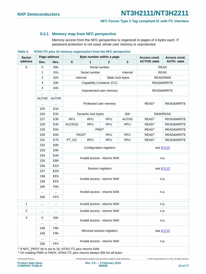
8.3.1 Memory map from NFC perspective
Memory access from the NFC perspective is organized in pages of 4 bytes each. If password protection is not used, whole user memory is unprotected.
Table 4. NTAG I2C plus 1k memory organization from the NFC perspective
Sectoraddress
Page address Byte number within a page Access cond.ACTIVE state
Access cond. AUTH. stateDec. Hex. 0 1 2 3
0 0 00h Serial number READ
1 01h Serial number Internal READ
2 02h Internal Static lock bytes READ/R&W
3 03h Capability Container (CC) READ&WRITE
4 04hUnprotected user memory READ&WRITE
... ...
AUTH0 AUTH0
Protected user memory READ1 READ&WRITE... ...
225 E1h
226 E2h Dynamic lock bytes 00h R&W/READ
227 E3h RFU RFU RFU AUTH0 READ1 READ&WRITE
228 E4h ACCESS RFU RFU RFU READ1 READ&WRITE
229 E5h PWD2 READ1 READ&WRITE
230 E6h PACK2 RFU RFU READ1 READ&WRITE
231 E7h PT_I2C RFU RFU RFU READ1 READ&WRITE
232 E8hConfiguration registers see 8.3.12
233 E9h
234 EAhInvalid access - returns NAK n.a.
235 EBh
236 EChSession registers see 8.3.12
237 EDh
238 EEhInvalid access - returns NAK n.a.
239 EFh
240 F0h
Invalid access - returns NAK n.a.... ...
255 FFh
1 ... ... Invalid access - returns NAK n.a.
2 ... ... Invalid access - returns NAK n.a.
3 0 00hInvalid access - returns NAK n.a.
... ...
248 F8hMirrored session registers see 8.3.12
249 F9h
... ...Invalid access - returns NAK n.a.
255 FFh1 If NFC_PROT bit is set to 1b, NTAG I2C plus returns NAK2 On reading PWD or PACK, NTAG I2C plus returns always 00h for all bytes
NT3H2111/NT3H2211 All information provided in this document is subject to legal disclaimers. © NXP Semiconductors N.V. 2016. All rights reserved.
Product data sheetCOMPANY PUBLIC
Rev. 3.0 — 3 February 2016359930 12 of 77
NXP Semiconductors NT3H2111/NT3H2211NFC Forum Type 2 Tag compliant IC with I2C interface
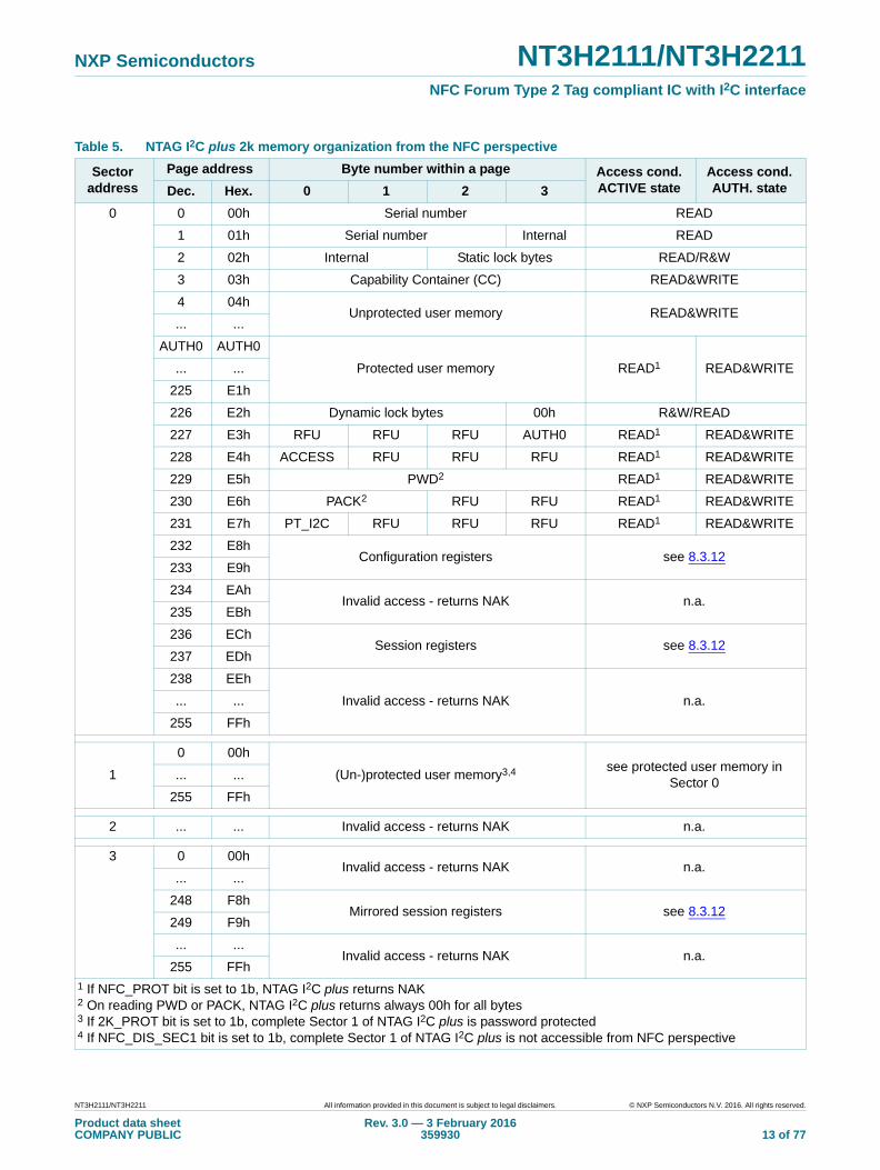
Table 5. NTAG I2C plus 2k memory organization from the NFC perspective
Sectoraddress
Page address Byte number within a page Access cond.ACTIVE state
Access cond. AUTH. stateDec. Hex. 0 1 2 3
0 0 00h Serial number READ
1 01h Serial number Internal READ
2 02h Internal Static lock bytes READ/R&W
3 03h Capability Container (CC) READ&WRITE
4 04hUnprotected user memory READ&WRITE
... ...
AUTH0 AUTH0
Protected user memory READ1 READ&WRITE... ...
225 E1h
226 E2h Dynamic lock bytes 00h R&W/READ
227 E3h RFU RFU RFU AUTH0 READ1 READ&WRITE
228 E4h ACCESS RFU RFU RFU READ1 READ&WRITE
229 E5h PWD2 READ1 READ&WRITE
230 E6h PACK2 RFU RFU READ1 READ&WRITE
231 E7h PT_I2C RFU RFU RFU READ1 READ&WRITE
232 E8hConfiguration registers see 8.3.12
233 E9h
234 EAhInvalid access - returns NAK n.a.
235 EBh
236 EChSession registers see 8.3.12
237 EDh
238 EEh
Invalid access - returns NAK n.a.... ...
255 FFh
1
0 00h
(Un-)protected user memory3,4 see protected user memory in Sector 0
... ...
255 FFh
2 ... ... Invalid access - returns NAK n.a.
3 0 00hInvalid access - returns NAK n.a.
... ...
248 F8hMirrored session registers see 8.3.12
249 F9h
... ...Invalid access - returns NAK n.a.
255 FFh1 If NFC_PROT bit is set to 1b, NTAG I2C plus returns NAK2 On reading PWD or PACK, NTAG I2C plus returns always 00h for all bytes3 If 2K_PROT bit is set to 1b, complete Sector 1 of NTAG I2C plus is password protected4 If NFC_DIS_SEC1 bit is set to 1b, complete Sector 1 of NTAG I2C plus is not accessible from NFC perspective
NT3H2111/NT3H2211 All information provided in this document is subject to legal disclaimers. © NXP Semiconductors N.V. 2016. All rights reserved.
Product data sheetCOMPANY PUBLIC
Rev. 3.0 — 3 February 2016359930 13 of 77
NXP Semiconductors NT3H2111/NT3H2211NFC Forum Type 2 Tag compliant IC with I2C interface
8.3.2 Memory map from I²C interface
The memory access of NTAG I2C plus from the I²C interface is organized in blocks of 16 bytes each.
NT3H2111/NT3H2211 All information provided in this document is subject to legal disclaimers. © NXP Semiconductors N.V. 2016. All rights reserved.
Product data sheetCOMPANY PUBLIC
Rev. 3.0 — 3 February 2016359930 14 of 77
NXP Semiconductors NT3H2111/NT3H2211NFC Forum Type 2 Tag compliant IC with I2C interface
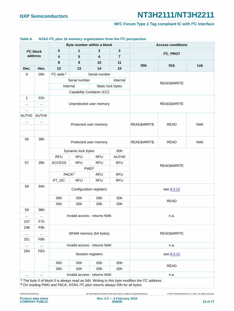
Table 6. NTAG I2C plus 1k memory organization from the I2C perspective
I2C blockaddress
Byte number within a block Access conditions
0 1 2 3I2C_PROT
4 5 6 7
8 9 10 1100b 01b 1xb
Dec. Hex. 12 13 14 15
0 00h I2C addr.1 Serial number
READ&WRITESerial number Internal
Internal Static lock bytes
Capability Container (CC)
1 01h
Unprotected user memory READ&WRITE... ...
... ...
AUTH0 AUTH0
Protected user memory READ&WRITE READ NAK... ...
56 38hProtected user memory READ&WRITE READ NAK
Dynamic lock bytes 00h
READ&WRITE
RFU RFU RFU AUTH0
57 39h ACCESS RFU RFU RFU
PWD2
PACK2 RFU RFU
PT_I2C RFU RFU RFU
58 3AhConfiguration registers see 8.3.12
00h 00h 00h 00hREAD
00h 00h 00h 00h
59 3Bh
Invalid access - returns NAK n.a.... ...
247 F7h
248 F8h
SRAM memory (64 bytes) READ&WRITE... ...
251 FBh
... ... Invalid access - returns NAK n.a.
254 FEhSession registers see 8.3.12
00h 00h 00h 00hREAD
00h 00h 00h 00h
... ... Invalid access - returns NAK n.a.1 The byte 0 of block 0 is always read as 04h. Writing to this byte modifies the I2C address.2 On reading PWD and PACK, NTAG I2C plus returns always 00h for all bytes
NT3H2111/NT3H2211 All information provided in this document is subject to legal disclaimers. © NXP Semiconductors N.V. 2016. All rights reserved.
Product data sheetCOMPANY PUBLIC
Rev. 3.0 — 3 February 2016359930 15 of 77
NXP Semiconductors NT3H2111/NT3H2211NFC Forum Type 2 Tag compliant IC with I2C interface
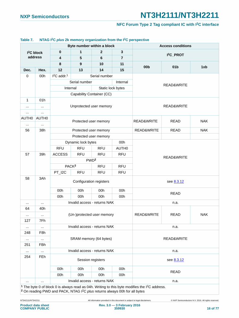
Table 7. NTAG I2C plus 2k memory organization from the I2C perspective
I2C blockaddress
Byte number within a block Access conditions
0 1 2 3I2C_PROT
4 5 6 7
8 9 10 1100b 01b 1xb
Dec. Hex. 12 13 14 15
0 00h I2C addr.1 Serial number
READ&WRITESerial number Internal
Internal Static lock bytes
Capability Container (CC)
1 01h
Unprotected user memory READ&WRITE... ...
... ...
AUTH0 AUTH0Protected user memory READ&WRITE READ NAK
... ...
56 38h Protected user memory READ&WRITE READ NAK
Protected user memory
Dynamic lock bytes 00h
READ&WRITE
RFU RFU RFU AUTH0
57 39h ACCESS RFU RFU RFU
PWD2
PACK2 RFU RFU
PT_I2C RFU RFU RFU
58 3AhConfiguration registers see 8.3.12
00h 00h 00h 00hREAD
00h 00h 00h 00h
... ... Invalid access - returns NAK n.a.
64 40h
(Un-)protected user memory READ&WRITE READ NAK... ...
127 7Fh
... ... Invalid access - returns NAK n.a.
248 F8h
SRAM memory (64 bytes) READ&WRITE... ...
251 FBh
... ... Invalid access - returns NAK n.a.
254 FEhSession registers see 8.3.12
00h 00h 00h 00hREAD
00h 00h 00h 00h
... ... Invalid access - returns NAK n.a.1 The byte 0 of block 0 is always read as 04h. Writing to this byte modifies the I2C address.2 On reading PWD and PACK, NTAG I2C plus returns always 00h for all bytes
NT3H2111/NT3H2211 All information provided in this document is subject to legal disclaimers. © NXP Semiconductors N.V. 2016. All rights reserved.
Product data sheetCOMPANY PUBLIC
Rev. 3.0 — 3 February 2016359930 16 of 77
NXP Semiconductors NT3H2111/NT3H2211NFC Forum Type 2 Tag compliant IC with I2C interface
8.3.3 EEPROM
The EEPROM is a non-volatile memory that stores the 7 byte UID, the memory lock conditions, IC configuration information and the 1912 bytes of user memory (888 byte user memory in case of the NTAG I2C plus 1k version).
Sector 0 memory map looks totally the same for NTAG I2C plus 1k and 2k version, the only difference is the dynamic lock bit granularity.
NXP introduced with NTAG I2C plus the possibility to split the memory in an open and a password protected area see Section 8.3.11.
8.3.4 SRAM
For frequently changing data, a volatile memory of 64 bytes with unlimited endurance is built in. The 64 bytes are mapped in a similar way as done in the EEPROM, i.e., 64 bytes are seen as 16 pages of 4 bytes from NFC perspective.
The SRAM is only available if the tag is powered via the VCC pin.
The SRAM is located at the end of the memory space and it is always directly accessible by the I2C host (addresses F8h to FBh). An NFC device cannot access the SRAM memory in normal mode (i.e., outside the pass-through mode). The SRAM is only accessible by the NFC device if the SRAM is mirrored onto the EEPROM memory space.
With SRAM mirror enabled (SRAM_MIRROR_ON_OFF = 1b - see Section 11.2), the SRAM can be mirrored in the User Memory from start page 01h to 74h for access from the NFC side.
The Memory mirror must be enabled once both interfaces are ON as this feature is disabled after each POR.
The register SRAM_MIRROR_BLOCK (see Table 14) indicates the address of the first page of the SRAM buffer. In the case where the SRAM mirror is enabled and the READ command is addressing blocks where the SRAM mirror is located, the SRAM byte values will be returned instead of the EEPROM byte values. Similarly, if the tag is not VCC powered, the SRAM mirror is disabled and reading out the bytes related to the SRAM mirror position would return the values from the EEPROM.
In the pass-through mode (PTHRU_ON_OFF = 1b - see Section 8.3.12), the SRAM is mirrored to the fixed address F0h - FFh for NFC access (see Section 11) in the first memory sector (Sector 0) for NTAG I2C plus.
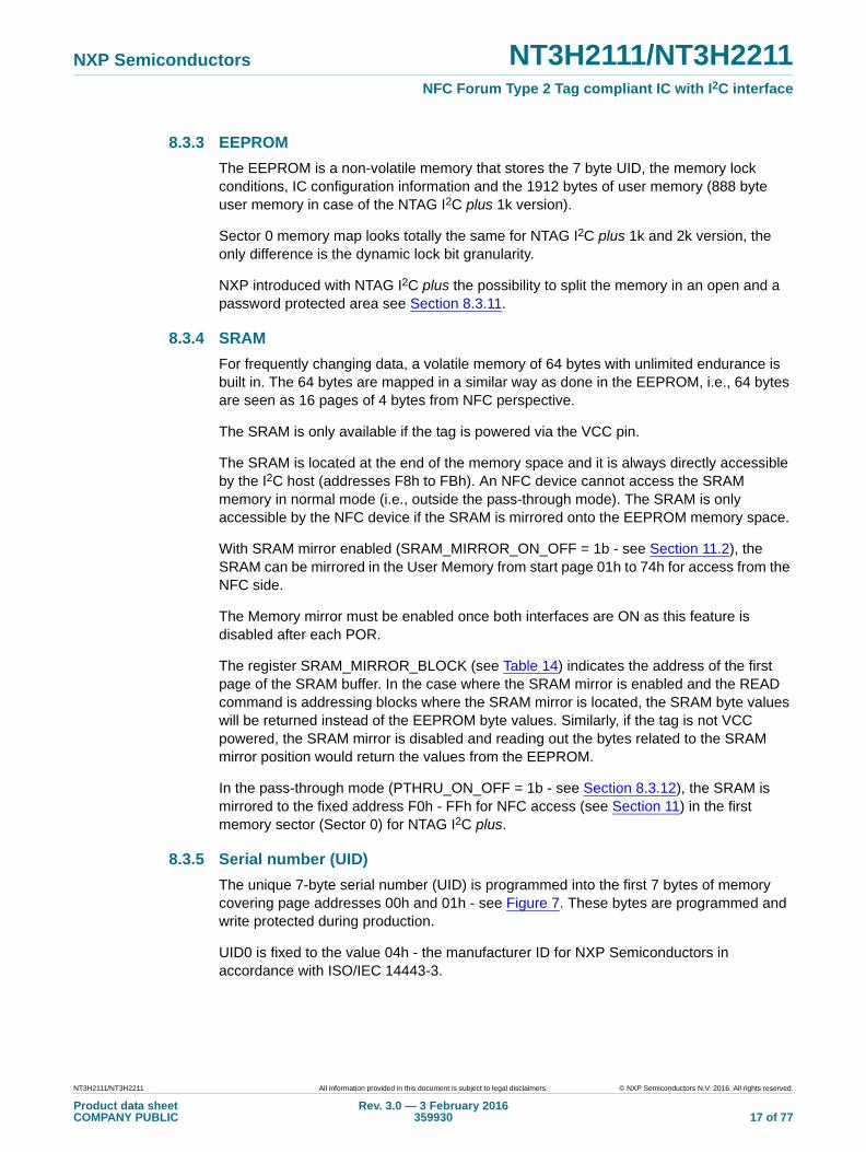
8.3.5 Serial number (UID)
The unique 7-byte serial number (UID) is programmed into the first 7 bytes of memory covering page addresses 00h and 01h - see Figure 7. These bytes are programmed and write protected during production.
UID0 is fixed to the value 04h - the manufacturer ID for NXP Semiconductors in accordance with ISO/IEC 14443-3.
NT3H2111/NT3H2211 All information provided in this document is subject to legal disclaimers. © NXP Semiconductors N.V. 2016. All rights reserved.
Product data sheetCOMPANY PUBLIC
Rev. 3.0 — 3 February 2016359930 17 of 77
NXP Semiconductors NT3H2111/NT3H2211NFC Forum Type 2 Tag compliant IC with I2C interface
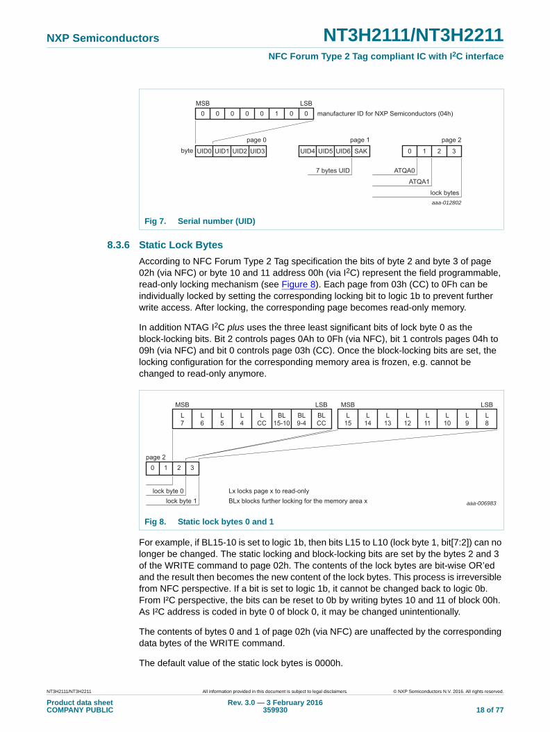
8.3.6 Static Lock Bytes
According to NFC Forum Type 2 Tag specification the bits of byte 2 and byte 3 of page 02h (via NFC) or byte 10 and 11 address 00h (via I2C) represent the field programmable, read-only locking mechanism (see Figure 8). Each page from 03h (CC) to 0Fh can be individually locked by setting the corresponding locking bit to logic 1b to prevent further write access. After locking, the corresponding page becomes read-only memory.
In addition NTAG I2C plus uses the three least significant bits of lock byte 0 as the block-locking bits. Bit 2 controls pages 0Ah to 0Fh (via NFC), bit 1 controls pages 04h to 09h (via NFC) and bit 0 controls page 03h (CC). Once the block-locking bits are set, the locking configuration for the corresponding memory area is frozen, e.g. cannot be changed to read-only anymore.
For example, if BL15-10 is set to logic 1b, then bits L15 to L10 (lock byte 1, bit[7:2]) can no longer be changed. The static locking and block-locking bits are set by the bytes 2 and 3 of the WRITE command to page 02h. The contents of the lock bytes are bit-wise OR’ed and the result then becomes the new content of the lock bytes. This process is irreversible from NFC perspective. If a bit is set to logic 1b, it cannot be changed back to logic 0b. From I²C perspective, the bits can be reset to 0b by writing bytes 10 and 11 of block 00h. As I²C address is coded in byte 0 of block 0, it may be changed unintentionally.
The contents of bytes 0 and 1 of page 02h (via NFC) are unaffected by the corresponding data bytes of the WRITE command.
The default value of the static lock bytes is 0000h.
Fig 7. Serial number (UID)
aaa-012802
MSB LSB
page 0byte
manufacturer ID for NXP Semiconductors (04h)0 0 0 0 0 1 0 0
UID0 UID1 UID2 UID3 UID4 UID5 UID6 SAK
page 1 page 2
0 1 2 3
ATQA1
ATQA07 bytes UID
lock bytes
Fig 8. Static lock bytes 0 and 1
L7
L6
L5
L4
LCC
BL15-10
BL9-4
BLCC
MSB
0page 2
Lx locks page x to read-onlyBLx blocks further locking for the memory area x
lock byte 0lock byte 1
1 2 3
LSBL
15L
14L
13L
12L11
L10
L9
L8
MSB LSB
aaa-006983
NT3H2111/NT3H2211 All information provided in this document is subject to legal disclaimers. © NXP Semiconductors N.V. 2016. All rights reserved.
Product data sheetCOMPANY PUBLIC
Rev. 3.0 — 3 February 2016359930 18 of 77
NXP Semiconductors NT3H2111/NT3H2211NFC Forum Type 2 Tag compliant IC with I2C interface
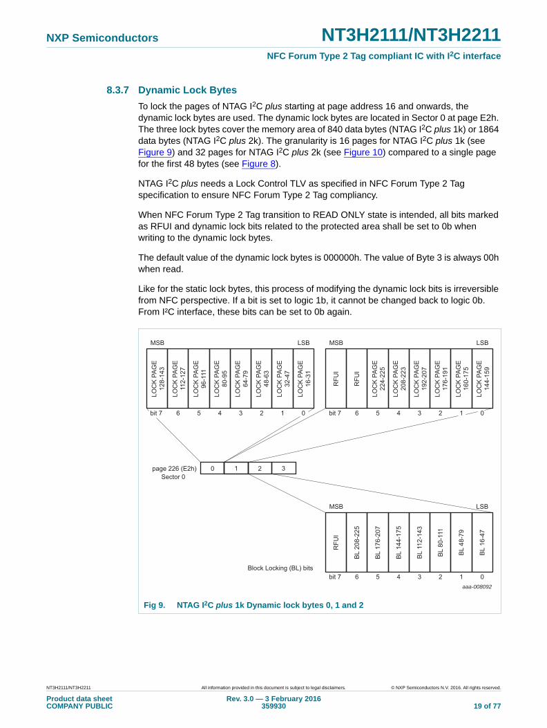
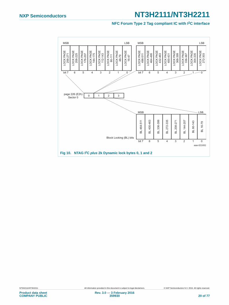
8.3.7 Dynamic Lock Bytes
To lock the pages of NTAG I2C plus starting at page address 16 and onwards, the dynamic lock bytes are used. The dynamic lock bytes are located in Sector 0 at page E2h. The three lock bytes cover the memory area of 840 data bytes (NTAG I2C plus 1k) or 1864 data bytes (NTAG I2C plus 2k). The granularity is 16 pages for NTAG I2C plus 1k (see Figure 9) and 32 pages for NTAG I2C plus 2k (see Figure 10) compared to a single page for the first 48 bytes (see Figure 8).
NTAG I2C plus needs a Lock Control TLV as specified in NFC Forum Type 2 Tag specification to ensure NFC Forum Type 2 Tag compliancy.
When NFC Forum Type 2 Tag transition to READ ONLY state is intended, all bits marked as RFUI and dynamic lock bits related to the protected area shall be set to 0b when writing to the dynamic lock bytes.
The default value of the dynamic lock bytes is 000000h. The value of Byte 3 is always 00h when read.
Like for the static lock bytes, this process of modifying the dynamic lock bits is irreversible from NFC perspective. If a bit is set to logic 1b, it cannot be changed back to logic 0b. From I²C interface, these bits can be set to 0b again.
Fig 9. NTAG I2C plus 1k Dynamic lock bytes 0, 1 and 2
aaa-008092
0 1 2 3page 226 (E2h)
LOC
K P
AG
E12
8-14
3
MSB LSB
bit 7 6
LOC
K P
AG
E11
2-12
7
LOC
K P
AG
E96
-111
LOC
K P
AG
E80
-95
LOC
K P
AG
E64
-79
LOC
K P
AG
E48
-63
LOC
K P
AG
E32
-47
LOC
K P
AG
E16
-31
LOC
K P
AG
E22
4-22
5
5 4 3 2 1 0
RFU
IMSB LSB
bit 7 6
RFU
I
LOC
K P
AG
E20
8-22
3
LOC
K P
AG
E19
2-20
7
LOC
K P
AG
E17
6-19
1
LOC
K P
AG
E16
0-17
5
LOC
K P
AG
E14
4-15
9
5 4 3 2 1 0
RFU
I
MSB LSB
bit 7 6
BL
208-
225
BL
176-
207
BL
144-
175
BL
112-
143
BL
80-1
11
BL
48-7
9
BL
16-4
7
5 4 3 2 1 0Block Locking (BL) bits
Sector 0
NT3H2111/NT3H2211 All information provided in this document is subject to legal disclaimers. © NXP Semiconductors N.V. 2016. All rights reserved.
Product data sheetCOMPANY PUBLIC
Rev. 3.0 — 3 February 2016359930 19 of 77
NXP Semiconductors NT3H2111/NT3H2211NFC Forum Type 2 Tag compliant IC with I2C interface
Fig 10. NTAG I2C plus 2k Dynamic lock bytes 0, 1 and 2
0 1 2 3page 226 (E2h)Sector 0
Block Locking (BL) bits
LOC
K P
AG
E25
6-27
1
MSB LSB
bit 7 6 5 4 3 2 1 0
MSB LSB
bit 7 6 5 4 3 2 1 0
MSB LSB
bit 7 6 5 4 3 2 1 0aaa-021651
LOC
K P
AG
E20
8-22
5
LOC
K P
AG
E17
6-20
7
LOC
K P
AG
E14
4-17
5
LOC
K P
AG
E11
2-14
3
LOC
K P
AG
E80
-111
LOC
K P
AG
E48
-79
LOC
K P
AG
E16
-47
BL
464-
511
LOC
K P
AG
E46
4-49
5
LOC
K P
AG
E49
6-51
1
LOC
K P
AG
E43
2-46
3
LOC
K P
AG
E40
0-43
1
LOC
K P
AG
E36
8-39
9
LOC
K P
AG
E33
6-36
7
LOC
K P
AG
E30
4-33
5
LOC
K P
AG
E27
2-30
3
BL
400-
463
BL
336-
399
BL
272-
335
BL
208-
271
BL
144-
207
BL
80-1
43
BL
16-7
9
NT3H2111/NT3H2211 All information provided in this document is subject to legal disclaimers. © NXP Semiconductors N.V. 2016. All rights reserved.
Product data sheetCOMPANY PUBLIC
Rev. 3.0 — 3 February 2016359930 20 of 77
NXP Semiconductors NT3H2111/NT3H2211NFC Forum Type 2 Tag compliant IC with I2C interface
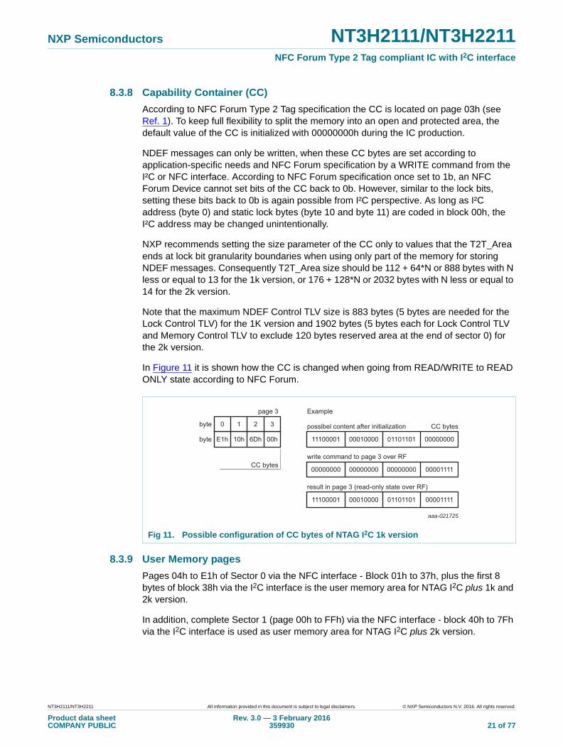
8.3.8 Capability Container (CC)
According to NFC Forum Type 2 Tag specification the CC is located on page 03h (see Ref. 1). To keep full flexibility to split the memory into an open and protected area, the default value of the CC is initialized with 00000000h during the IC production.
NDEF messages can only be written, when these CC bytes are set according to application-specific needs and NFC Forum specification by a WRITE command from the I²C or NFC interface. According to NFC Forum specification once set to 1b, an NFC Forum Device cannot set bits of the CC back to 0b. However, similar to the lock bits, setting these bits back to 0b is again possible from I²C perspective. As long as I²C address (byte 0) and static lock bytes (byte 10 and byte 11) are coded in block 00h, the I²C address may be changed unintentionally.
NXP recommends setting the size parameter of the CC only to values that the T2T_Area ends at lock bit granularity boundaries when using only part of the memory for storing NDEF messages. Consequently T2T_Area size should be 112 + 64*N or 888 bytes with N less or equal to 13 for the 1k version, or 176 + 128*N or 2032 bytes with N less or equal to 14 for the 2k version.
Note that the maximum NDEF Control TLV size is 883 bytes (5 bytes are needed for the Lock Control TLV) for the 1K version and 1902 bytes (5 bytes each for Lock Control TLV and Memory Control TLV to exclude 120 bytes reserved area at the end of sector 0) for the 2k version.
In Figure 11 it is shown how the CC is changed when going from READ/WRITE to READ ONLY state according to NFC Forum.
8.3.9 User Memory pages
Pages 04h to E1h of Sector 0 via the NFC interface - Block 01h to 37h, plus the first 8 bytes of block 38h via the I2C interface is the user memory area for NTAG I2C plus 1k and 2k version.
In addition, complete Sector 1 (page 00h to FFh) via the NFC interface - block 40h to 7Fh via the I2C interface is used as user memory area for NTAG I2C plus 2k version.
Fig 11. Possible configuration of CC bytes of NTAG I2C 1k version
aaa-021725
byte E1h 10h 6Dh 00h
Example
CC bytes
CC bytes
byte 0 1 2 3
page 3
possibel content after initialization
11100001 00010000 01101101 00000000
write command to page 3 over RF
00000000 00000000 00000000 00001111
result in page 3 (read-only state over RF)
11100001 00010000 01101101 00001111
NT3H2111/NT3H2211 All information provided in this document is subject to legal disclaimers. © NXP Semiconductors N.V. 2016. All rights reserved.
Product data sheetCOMPANY PUBLIC
Rev. 3.0 — 3 February 2016359930 21 of 77
NXP Semiconductors NT3H2111/NT3H2211NFC Forum Type 2 Tag compliant IC with I2C interface
8.3.10 Memory content at delivery
As described above the CC in page 03h is set to all 00h to keep the full flexibility. To allow NFC Forum NDEF message reading and writing page 03h (CC) and the following data page (NDEF TLV) of NTAG I2C plus need to be initialized by the user according to the NFC Forum Type 2 Tag specification (see Ref. 1). Table 8 shows an example of NFC Forum-compliant content using the whole memory of sector 0 for NDEF messages.
Remark: The default content of the data pages from page 04h onwards is not defined at delivery.
Table 8. Minimum memory content to be in initialized state for NTAG I2C plus
Page Address Byte number within page
0 1 2 3
03h E1h 10h 6Dh 00h
04h 03h 00h FEh 00h
NT3H2111/NT3H2211 All information provided in this document is subject to legal disclaimers. © NXP Semiconductors N.V. 2016. All rights reserved.
Product data sheetCOMPANY PUBLIC
Rev. 3.0 — 3 February 2016359930 22 of 77
NXP Semiconductors NT3H2111/NT3H2211NFC Forum Type 2 Tag compliant IC with I2C interface
8.3.11 Password and Access Configuration
NTAG I2C plus can be configured to have password protected memory areas.
If this feature is used, NXP recommends changing and diversify the PWD and PACK for every single chip.
The password and access configuration area of pages E3h to E7h (Sector 0 - see Table 9) via the NFC interface or blocks 38h and 39h via the I2C interface are used to configure the password and access conditions of the NTAG I2C plus. Those bit values are stored in the EEPROM. Their values can be read and written by both interfaces when applicable and when not locked by the register lock bits (see REG_LOCK in Table 13).
AUTH0 defines the starting page address of the protected area in Sector 0. NXP recommends setting AUTH0 in a way always respecting the lock bit granularity. Setting AUTH0 greater EBh, disables password protection.
The NFC_PROT bit is used to either only require a PWD_AUTH for writing data to the protected area or even protect reading data from the protected area.
If password authentication is used, even the SRAM access can be protected by setting SRAM_PROT bit to 1b.
I2C_PROT enables the possibility to limit access to the protected area from I2C perspective to read only or no access at all.
AUTLIM value can be used to limit negative PWD_AUTH attempts.
For the 2k version of NTAG I2C plus NFC_DIS_SEC1 bit can be used to disable the access to Sector 1 from NFC perspective with the 2K_PROT bit password protection for Sector 1 can be enabled.
Once password protection is enabled, writing to Password and Access Configuration bytes is only possible after a successful password authentication. On reading the PWD or PACK, from NFC or I²C perspective, NTAG I2C plus always returns all 00h bytes.
A detailed description of the mechanism and how to program all the parameters is given in Section 8.7.
Table 9. Password and Access Configuration Register
NFC page address(Sector 0)
I2C block address Byte number from NFC perspective
Dec Hex Dec Hex 0 1 2 3
224 E0h 56 38hUser Memory
225 E1h
226 E2h Dynamic lock bytes 00h
227 E3h RFU RFU RFU AUTH0
228 E4h 57 39h ACCESS RFU RFU RFU
229 E5h PWD
230 E6h PACK RFU RFU
231 E7h PT_I2C RFU RFU RFU
NT3H2111/NT3H2211 All information provided in this document is subject to legal disclaimers. © NXP Semiconductors N.V. 2016. All rights reserved.
Product data sheetCOMPANY PUBLIC
Rev. 3.0 — 3 February 2016359930 23 of 77
NXP Semiconductors NT3H2111/NT3H2211NFC Forum Type 2 Tag compliant IC with I2C interface
Table 10. Password and Access Configuration bytes
Bit Field Accessvia NFC
Accessvia I²C
Defaultvalues
Description
Authentication Pointer (AUTH0)
7-0 AUTH0 R&W R&W FFh Page address of Sector 0 from which onwards the password authentication is required to access the user memory from NFC perspective, dependent on NFC_PROT bit.
If AUTH0 is set to a page address greater than EBh, the password protection is effectively disabled. Password protected area starts from page AUTH0 and ends at page EBh.
Password protection is excluded for Dynamic Lock Bits, session registers and mirrored SRAM pages.
Note: From I²C interface, you have access to all configuration pages until REG_LOCK_I2C bit is set to 1b.
Access Conditions (ACCESS)
7 NFC_PROT R&W R&W 0b Memory protection bit:
0b: write access to protected area is protected by the password
1b: read and write access to protected area is protected by the password
6 RFU R R 0b RFU - keep at 0b
5 NFC_DIS_SEC1 R&W R&W 0b NFC access protection to Sector 1
0b: Sector 1 is accessible in 2k version
1b: Sector 1 in inaccessible and returns NAK0
4-3 RFU R R 00b RFU - keep at 00b
2-0 AUTHLIM R&W R&W 000b Limitation of negative password authentication attempts. After reaching the limit, protected area is not accessible any longer.
000b: limiting of negative password authentication attempts disabled.
001b-111b: maximum number of negative password authentication attempts is 2AUTHLIM
Password (PWD)
31-0 PWD R&W R&W FFFFFFFFh 32-bit password used for memory access protection.
Reading PWD always returns 00000000h
Password Acknowledge (PACK)
15-0 PACK R&W R&W 0000h 16-bit password acknowledge used during the password authentication process.
Reading PACK always returns 0000h
Protection bits (PT_I2C)
7-4 RFU R R 0000b RFU - keep at 0000b
NT3H2111/NT3H2211 All information provided in this document is subject to legal disclaimers. © NXP Semiconductors N.V. 2016. All rights reserved.
Product data sheetCOMPANY PUBLIC
Rev. 3.0 — 3 February 2016359930 24 of 77
NXP Semiconductors NT3H2111/NT3H2211NFC Forum Type 2 Tag compliant IC with I2C interface
8.3.12 NTAG I2C configuration and session registers
NTAG I2C plus behavior can be configured and read in two separate locations depending if the configurations shall be effective within the communication session (use session registers) or by default after Power-On Reset (POR) (use configuration registers).
The configuration registers of pages E8h to E9h (Sector 0 - see Table 11) via the NFC interface or block 3Ah via the I2C interface are used to configure the default behavior of the NTAG I2C plus. Those bit values are stored in the EEPROM and represent the default settings to be effective after POR. Their values can be read and written by both interfaces when applicable and when not locked by the register lock bits (see REG_LOCK in Table 13).
The session register on pages ECh to EDh (Sector 0) via the NFC interface or block FEh via I2C, see Table 12, are used to configure or monitor the values of the current communication session. Those bits are read only via the NFC interface but may be read and written via the I2C interface.
For backward compatibility reasons the session registers are mirrored to Sector 3 (page F8h and F9h via the NFC interface).
3 2K_PROT R&W R&W 0b Password protection for Sector 1 for 2k version
0b: password authentication for Sector 1 disabled
1b: password authentication needed to access Sector 1
2 SRAM_PROT R&W R&W 0b Password protection for pass-through and mirror mode 0b: password authentication for pass-through mode disabled1b: password authentication needed to access SRAM in pass-through mode
1-0 I2C_PROT R&W R&W 00b Access to protected area from I²C perspective
00b: Entire user memory accessible from I2C
01b: read and write access to unprotected user area, read only access to protected area
1Xb: read and write access to unprotected area, no access to protected area.
Note: Independent from these bits I2C has always R/W access to:
• Session registers
• SRAM
• Configuration pages including PWD Configuration area, but dependent on REG_LOCK_I2C bit
Table 10. …continuedPassword and Access Configuration bytes
Bit Field Accessvia NFC
Accessvia I²C
Defaultvalues
Description
Table 11. Configuration register NTAG I2C plus
NFC address (Sector 0)
I2C Address Byte number from NFC perspective
Dec Hex Dec Hex 0 1 2 3
232 E8h 58 3Ah NC_REG LAST_NDEF_BLOCK SRAM_MIRROR_BLOCK WDT_LS
233 E9h WDT_MS I2C_CLOCK_STR REG_LOCK RFU
NT3H2111/NT3H2211 All information provided in this document is subject to legal disclaimers. © NXP Semiconductors N.V. 2016. All rights reserved.
Product data sheetCOMPANY PUBLIC
Rev. 3.0 — 3 February 2016359930 25 of 77
NXP Semiconductors NT3H2111/NT3H2211NFC Forum Type 2 Tag compliant IC with I2C interface
Both, the session and the configuration registers have the same configuration options and parameters except the REG_LOCK bits, which are only available in the configuration register and the NS_REG bits which are only available in the session register. After POR, the content of the configuration register is loaded into the session register.
The values of both registers can be changed during a communication session. If the desired effect should be visible immediately, but only for the current communication session, the session registers must be used. After POR, the session registers values will again contain the configuration register values as before.
To change the default behavior, changes to the configuration register are needed, but the related effect will only be visible after the next POR.
To make the effect immediately and after next POR visible, changes to configuration and session registers are needed.
All registers and configuration default values, access conditions and descriptions are defined in Table 13 and Table 14.
Reading and writing the session registers via I²C can only be done via the READ and WRITE registers operation - see Section 9.8.
Table 12. Session registers NTAG I2C plus
NFC address (Sector 0)
I2C Address Byte number
Dec Hex Dec Hex 0 1 2 3
236 ECh 254 FEh NC_REG LAST_NDEF_BLOCK SRAM_MIRROR _BLOCK WDT_LS
237 EDh WDT_MS I2C_CLOCK_STR NS_REG RFU
NT3H2111/NT3H2211 All information provided in this document is subject to legal disclaimers. © NXP Semiconductors N.V. 2016. All rights reserved.
Product data sheetCOMPANY PUBLIC
Rev. 3.0 — 3 February 2016359930 26 of 77
NXP Semiconductors NT3H2111/NT3H2211NFC Forum Type 2 Tag compliant IC with I2C interface
Table 13. Configuration bytes
Bit Field Access via NFC
Access via I²C
Default values
Description
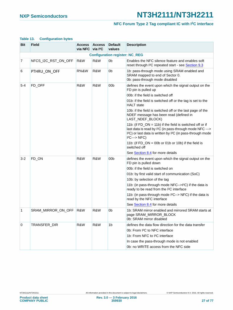
Configuration register: NC_REG
7 NFCS_I2C_RST_ON_OFF R&W R&W 0b Enables the NFC silence feature and enables soft reset through I²C repeated start - see Section 9.3
6 PTHRU_ON_OFF R%&W R&W 0b 1b: pass-through mode using SRAM enabled and SRAM mapped to end of Sector 0.0b: pass-through mode disabled
5-4 FD_OFF R&W R&W 00b defines the event upon which the signal output on the FD pin is pulled up
00b: if the field is switched off
01b: if the field is switched off or the tag is set to the HALT state
10b: if the field is switched off or the last page of the NDEF message has been read (defined in LAST_NDEF_BLOCK)
11b: (if FD_ON = 11b) if the field is switched off or if last data is read by I²C (in pass-through mode NFC ---> I²C) or last data is written by I²C (in pass-through mode I²C---> NFC)
11b: (if FD_ON = 00b or 01b or 10b) if the field is switched off
See Section 8.4 for more details
3-2 FD_ON R&W R&W 00b defines the event upon which the signal output on the FD pin is pulled down
00b: if the field is switched on
01b: by first valid start of communication (SoC)
10b: by selection of the tag
11b: (in pass-through mode NFC-->I²C) if the data is ready to be read from the I²C interface
11b: (in pass-through mode I²C--> NFC) if the data is read by the NFC interface
See Section 8.4 for more details
1 SRAM_MIRROR_ON_OFF R&W R&W 0b 1b: SRAM mirror enabled and mirrored SRAM starts at page SRAM_MIRROR_BLOCK0b: SRAM mirror disabled
0 TRANSFER_DIR R&W R&W 1b defines the data flow direction for the data transfer
0b: From I²C to NFC interface
1b: From NFC to I²C interface
In case the pass-through mode is not enabled
0b: no WRITE access from the NFC side
NT3H2111/NT3H2211 All information provided in this document is subject to legal disclaimers. © NXP Semiconductors N.V. 2016. All rights reserved.
Product data sheetCOMPANY PUBLIC
Rev. 3.0 — 3 February 2016359930 27 of 77

NXP Semiconductors NT3H2111/NT3H2211NFC Forum Type 2 Tag compliant IC with I2C interface
Configuration register: LAST_NDEF_BLOCK
7-0 LAST_NDEF_BLOCK R&W R&W 00h I²C block address of I²C block, which contains last byte(s) of stored NDEF message. An NFC read of the last page of this I²C block sets the register NDEF_DATA_READ to 1b and triggers field detection pin if FD_OFF is set to 10b.
Valid range starts from 01h (NFC page 04h) up to 37h (NFC page DCh) for NTAG I2C plus 1k or up to 7Fh (NFC page FCh on Sector 1) for NTAG I2C plus 2k.
Configuration register: SRAM_MIRROR_BLOCK
7-0 SRAM_MIRROR_BLOCK R&W R&W F8h I²C block address of SRAM when mirrored into the User memory.
Valid range starts
from 01h (NFC page 04h) up to 34h (NFC page D0h) for NTAG I2C plus 1k or up to 7Ch (NFC page F0h on memory Sector 1) for NTAG I2C plus 2k
Configuration register: WDT_LS
7-0 WDT_LS R&W R&W 48h Least Significant byte of watchdog time control register
Configuration register: WDT_MS
7-0 WDT_MS R&W R&W 08h Most Significant byte of watchdog time control register.When writing WDT_MS byte, the content of WDT_MS and WDT_LS gets active for the watchdog timer.
Configuration register: I2C_CLOCK_STR
7-1 RFU READ READ 0000000b RFU - all 7 bits locked to 0b
0 I2C_CLOCK_STR R&W R&W 1b Enables (1b) or disable (0b) the I²C clock stretching
Configuration register: REG_LOCK
7-2 RFU READ READ 000000b RFU - all 6 bits locked to 0b
1 REG_LOCK_I2C1 R&W R&W 0b I²C Configuration Lock Bit0b: Configuration bytes may be changed via I²C
1b: Configuration bytes can not be changed via I²C
Once set to 1b, cannot be reset to 0b anymore.
0 REG_LOCK_NFC1 R&W R&W 0b NFC Configuration Lock Bit0b: Configuration bytes may be changed via NFC
1b… Configuration bytes can not be changed via NFC
Once set to 1b, cannot be reset to 0b anymore.1 Setting both bits REG_LOCK_I2C and REG_LOCK_NFC to 1b, permanently locks write access to register default values (as no write is allowed anymore). As long as one bit is still 0b, the corresponding interface can still access and change the register lock bytes.
Table 13. …continuedConfiguration bytes
Bit Field Access via NFC
Access via I²C
Default values
Description
NT3H2111/NT3H2211 All information provided in this document is subject to legal disclaimers. © NXP Semiconductors N.V. 2016. All rights reserved.
Product data sheetCOMPANY PUBLIC
Rev. 3.0 — 3 February 2016359930 28 of 77
NXP Semiconductors NT3H2111/NT3H2211NFC Forum Type 2 Tag compliant IC with I2C interface
Table 14. Session register bytes
Bit Field Access via NFC
Access via I²C
Default values
Description
Session register: NC_REG
7 NFCS_I2C_RST_ON_OFF READ R&W - see configuration bytes description
6 PTHRU_ON_OFF READ R&W - see configuration bytes description, the bit is cleared automatically, when on of the interfaces is OFF:
5-4 FD_OFF READ R&W - see configuration bytes description
3-2 FD_ON READ R&W
1 SRAM_MIRROR_ON_OFF READ R&W - see configuration bytes description, the bit is cleared automatically, when there is no Vcc power.
0 TRANSFER_DIR READ R&W see configuration bytes description
Session register: LAST_NDEF_BLOCK
7-0 LAST_NDEF_BLOCK READ R&W - see configuration bytes description
Session register: SRAM_MIRROR_BLOCK
7-0 SRAM_MIRROR_BLOCK READ R&W - see configuration bytes description
Session register: WDT_LS
7-0 WDT_LS READ R&W - see configuration bytes description
Session register: WDT_MS
7-0 WDT_MS READ R&W - see configuration bytes description
Session register: I2C_CLOCK_STR
7-2 RFU READ READ - RFU, all 6 bits locked to 0b
1 NEG_AUTH_REACHED READ READ 0b Status bit to show the number of negative PWD_AUTH attempts reached0b: PWD_AUTH still possible1b: PWD_AUTH locked
0 I2C_CLOCK_STR READ READ - See configuration bytes description
Session register: NS_REG
7 NDEF_DATA_READ READ READ 0b 1b: all data bytes read from the address specified in LAST_NDEF_BLOCK. Bit is reset to 0b when read
6 I2C_LOCKED READ R&W 0b 1b: Memory access is locked to the I²C interface
5 RF_LOCKED READ READ 0b 1b: Memory access is locked to the NFC interface
4 SRAM_I2C_READY READ READ 0b 1b: data is ready in SRAM buffer to be read by I2C
3 SRAM_RF_READY READ READ 0b 1b: data is ready in SRAM buffer to be read by NFC
2 EEPROM_WR_ERR READ R&W 0b 1b: HV voltage error during EEPROM write or erase cycleNeeds to be written back via I²C to 0b to be cleared
1 EEPROM_WR_BUSY READ READ 0b 1b: EEPROM write cycle in progress - access to EEPROM disabled
0b: EEPROM access possible
0 RF_FIELD_PRESENT READ READ 0b 1b: NFC field is detected
NT3H2111/NT3H2211 All information provided in this document is subject to legal disclaimers. © NXP Semiconductors N.V. 2016. All rights reserved.
Product data sheetCOMPANY PUBLIC
Rev. 3.0 — 3 February 2016359930 29 of 77
NXP Semiconductors NT3H2111/NT3H2211NFC Forum Type 2 Tag compliant IC with I2C interface
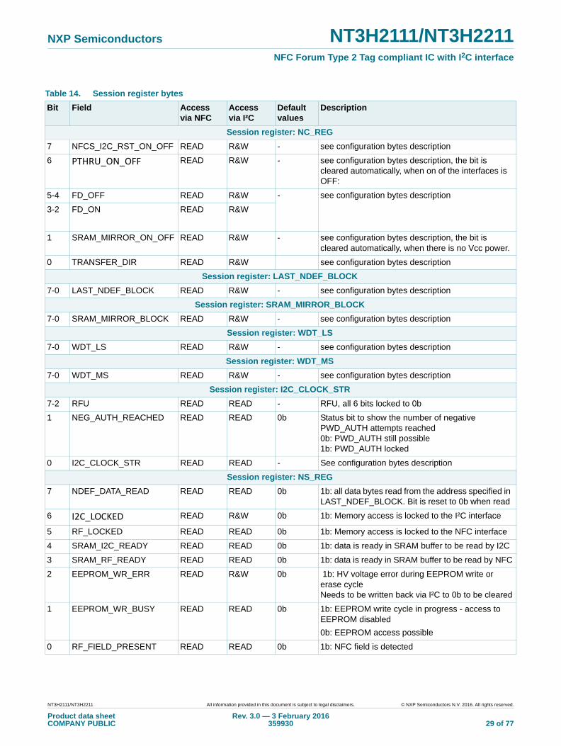
8.4 Configurable Event Detection Pin
The event detection feature provides the capability to trigger an external device (e.g. Controller) or switch on the connected circuitry by an external power management unit depending on activities on the NFC interface.
The conditions for the activation of the field detection signal defined with FD_ON can be:
• The presence of the NFC field
• The detection of a valid command (Start of Communication)
• The selection of the IC
The conditions for the de-activation of the field detection signal defined with FD_OFF can be:
• The absence of the NFC field
• The detection of the HALT state
• The NFC interface has read the last part of the NDEF message defined with LAST_NDEF_BLOCK
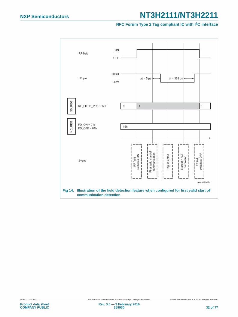
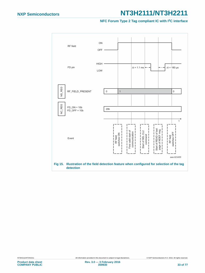
All the various combinations of configurations are described in Table 13 and illustrated in Figure 13, Figure 14 and Figure 15 for all various combinations of the filed detection signal configuration. The timing diagrams are not in scale and all given timing values are typical values.
The field detection pin can also be used as a handshake mechanism in the pass-through mode to signal to the external Controller if
• New data is written to SRAM on the NFC interface
• Data written to SRAM from the Controller is read via the NFC interface.
See Section 11 for more information on this handshake mechanism.
In Figure 12 an example how to connect the FD pin is given. All given values are typical values and may vary from application to application.
Fig 12. FD pin example circuit
LA LB
VSS VOUT
SCLGND
VCC
FDevent detect signal
APPLICATION
SDA
aaa-021652
1
2
3
4
6
5
8
7Rpu>2 kΩ
supply(1.2 V ~ 3.6 V)
NT3H2111/NT3H2211 All information provided in this document is subject to legal disclaimers. © NXP Semiconductors N.V. 2016. All rights reserved.
Product data sheetCOMPANY PUBLIC
Rev. 3.0 — 3 February 2016359930 30 of 77
NXP Semiconductors NT3H2111/NT3H2211NFC Forum Type 2 Tag compliant IC with I2C interface
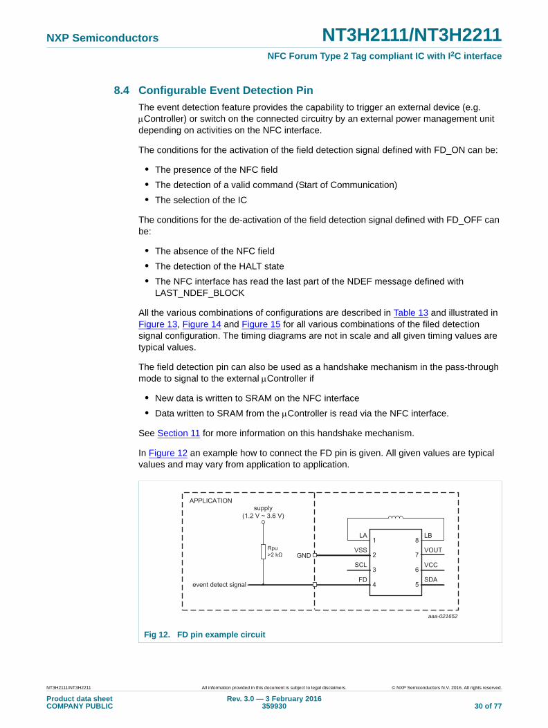
Fig 13. Illustration of the field detection feature when configured for simple field detection
aaa-021653
RF
field
switc
hes
ON
Firs
t val
id s
tart
ofco
mm
unic
atio
n
Tag
sele
cted
Tag
set t
o H
ALT
RF
field
switc
hes
OFF
ON
OFF
HIGH
LOW∆t = 180 μs ∆t = 16 μs
RF field
FD pin
Event
0
01h
t
0
FD_ON = 00bFD_OFF = 00b
NC
_RE
G
RF_FIELD_PRESENT
NS
_RE
G
1
NT3H2111/NT3H2211 All information provided in this document is subject to legal disclaimers. © NXP Semiconductors N.V. 2016. All rights reserved.
Product data sheetCOMPANY PUBLIC
Rev. 3.0 — 3 February 2016359930 31 of 77
NXP Semiconductors NT3H2111/NT3H2211NFC Forum Type 2 Tag compliant IC with I2C interface
Fig 14. Illustration of the field detection feature when configured for first valid start of communication detection
aaa-021654
RF
field
switc
hes
ON
Firs
t val
id s
tart
ofco
mm
unic
atio
n
Tag
sele
cted
RF
field
switc
hes
OFF
ON
OFF
HIGH
LOW∆t = 5 μs ∆t = 368 μs
RF field
FD pin
Event
0
15h
t
0
FD_ON = 01bFD_OFF = 01b
NC
_RE
G
RF_FIELD_PRESENT
NS
_RE
G
Sta
rt of
HA
LTco
mm
and
1
NT3H2111/NT3H2211 All information provided in this document is subject to legal disclaimers. © NXP Semiconductors N.V. 2016. All rights reserved.
Product data sheetCOMPANY PUBLIC
Rev. 3.0 — 3 February 2016359930 32 of 77
NXP Semiconductors NT3H2111/NT3H2211NFC Forum Type 2 Tag compliant IC with I2C interface
Fig 15. Illustration of the field detection feature when configured for selection of the tag detection
aaa-021655
RF
field
switc
hes
ON
Firs
t val
id s
tart
ofco
mm
unic
atio
n
RF
field
switc
hes
OFF
ON
OFF
HIGH
LOW∆t = 1.1 ms ∆t = 180 μs
RF field
FD pin
Event
0
29h
t
0
FD_ON = 10bFD_OFF = 10b
NC
_RE
G
RF_FIELD_PRESENT
NS
_RE
G
Sta
rt of
SE
L C
L2co
mm
and
Sta
rt of
RE
AD
of l
ast
page
of N
DE
F m
sg.
1
NT3H2111/NT3H2211 All information provided in this document is subject to legal disclaimers. © NXP Semiconductors N.V. 2016. All rights reserved.
Product data sheetCOMPANY PUBLIC
Rev. 3.0 — 3 February 2016359930 33 of 77

NXP Semiconductors NT3H2111/NT3H2211NFC Forum Type 2 Tag compliant IC with I2C interface
8.5 Watchdog timer
In order to allow the I²C interface to perform all necessary commands (READ, WRITE, ..), the memory access remains locked to the I²C interface until the register I2C_LOCKED is cleared by the host - see Table 14.
However, to avoid that the memory stays 'locked' to the I²C for a long period of time, it is possible to program a watchdog timer to unlock the I2C host from the tag, so that the NFC device can access the tag after a period of time of inactivity. The host itself will not be notified of this event directly, but the NS_REG register is updated accordingly (the register bit I2C_LOCKED will be cleared - see Table 14).
The default value is set to 20 ms (848h), but the watch dog timer can be freely set from 0001h (9.43 s) up to FFFFh (617.995 ms). The timer starts ticking when the communication between the NTAG I2C and the I2C interface starts. In case the communication with the I2C is still going on after the watchdog timer expires, the communication will continue until the communication has completed. Then the status register I2C_LOCKED will be immediately cleared.
In the case where the communication with the I2C interface has completed before the end of the timer and the status register I2C_LOCKED was not cleared by the host, it will be cleared at the end of the watchdog timer.
The watchdog timer is only effective if the VCC pin is powered and will be reset and stopped if the NTAG I2C is not VCC powered or if the register status I2C_LOCKED is set to 0 and RF_LOCKED is set to 1.
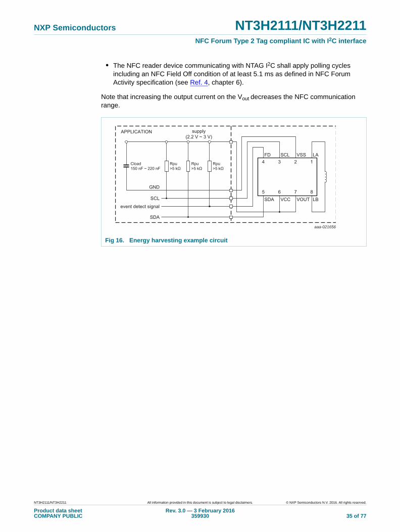
8.6 Energy harvesting
The NTAG I2C plus provides the capability to supply external low-power devices with energy harvested from the NFC field of an NFC device as illustrated in Figure 16. All given values are typical values. For more details refer to Ref. 7.
The voltage and current from the energy harvesting depend on various parameters, such as the strength of the NFC field, the tag antenna size, or the distance from the NFC device. NTAG I2C plus provides typically 5 mA at 2 V on the VOUT pin with an NFC Phone.
Operating NTAG I2C in energy harvesting mode requires a number of precautions:
• A complete total connected capacitor in the range of typically 150 nF up to 220 nF maximum shall be connected between VOUT and GND close to the terminals to ensure that the voltage does not drop below VCC min during modulation or during any application operation.
• Start up load current on VOUT should be limited until sufficient voltage is built on VOUT.
• If NTAG I2C also powers the I2C bus, then VCC must be connected to VOUT, and pull-up resistors on the SCL and SDA pins must be sized to control SCL and SDA sink current when those lines are pulled low by NTAG I2C or the I2C host
• If NTAG I2C also powers the Field Detect bus, then the pull-up resistor on the Field Detect line must be sized to control the sink current into the Field Detect pin when NTAG I2C pulls it low
NT3H2111/NT3H2211 All information provided in this document is subject to legal disclaimers. © NXP Semiconductors N.V. 2016. All rights reserved.
Product data sheetCOMPANY PUBLIC
Rev. 3.0 — 3 February 2016359930 34 of 77
NXP Semiconductors NT3H2111/NT3H2211NFC Forum Type 2 Tag compliant IC with I2C interface
• The NFC reader device communicating with NTAG I2C shall apply polling cycles including an NFC Field Off condition of at least 5.1 ms as defined in NFC Forum Activity specification (see Ref. 4, chapter 6).
Note that increasing the output current on the Vout decreases the NFC communication range.
Fig 16. Energy harvesting example circuit
LA
LB
VSS
VOUT
SCL
VCC
FD
event detect signal
SDA
SCL
GND
SDA
aaa-021656
14 3 2
85 6 7
Rpu>5 kΩ
Rpu>5 kΩ
Rpu>5 kΩ
supply(2.2 V ~ 3 V)
Cload150 nF ~ 220 nF
APPLICATION
NT3H2111/NT3H2211 All information provided in this document is subject to legal disclaimers. © NXP Semiconductors N.V. 2016. All rights reserved.
Product data sheetCOMPANY PUBLIC
Rev. 3.0 — 3 February 2016359930 35 of 77
NXP Semiconductors NT3H2111/NT3H2211NFC Forum Type 2 Tag compliant IC with I2C interface
8.7 Password authentication
The memory write or read/write access to a configurable part of the memory can be constrained to a positive password authentication. The 32-bit secret password (PWD) and the 16-bit password acknowledge (PACK) response shall be typically programmed into the configuration pages at the tag personalization stage.
The AUTHLIM parameter specified in Section 8.3.11 can be used to limit the negative authentication attempts.
In the initial state of NTAG I2C plus, password protection is disabled by an AUTH0 value of FFh. PWD and PACK are freely writable in this state. Access to the configuration pages and any part of the user memory can be restricted by setting AUTH0 to a page address within the available memory space. This page address is the first one protected.
For a comprehensive description of all protection mechanism refer to Ref. 9.
Remark: The password protection method provided in NTAG I2C plus has to be intended as an easy and convenient way to prevent unauthorized memory accesses. If a higher level of protection is required, cryptographic methods can be implemented at application layer to increase overall system security.
8.7.1 Programming of PWD and PACK
The 32-bit PWD and the 16-bit PACK need to be programmed into the configuration pages, see Section 8.3.11. The password as well as the password acknowledge are written LSByte first. This byte order is the same as the byte order used during the PWD_AUTH command and its response.
The PWD and PACK bytes can never be read out of the memory. Instead of transmitting the real value on any valid read command from both - NFC and I²C - interface, only 00h bytes are replied.
If the password authentication is disabled, PWD and PACK can be written at any time.
If the password authentication is enabled, PWD and PACK can be written after a successful PWD_AUTH command only.
Remark: To improve the overall system security, it is advisable to diversify the password and the password acknowledge using a die individual parameter of the IC, which is the 7-byte UID available on NTAG I2C plus.
NT3H2111/NT3H2211 All information provided in this document is subject to legal disclaimers. © NXP Semiconductors N.V. 2016. All rights reserved.
Product data sheetCOMPANY PUBLIC
Rev. 3.0 — 3 February 2016359930 36 of 77
NXP Semiconductors NT3H2111/NT3H2211NFC Forum Type 2 Tag compliant IC with I2C interface
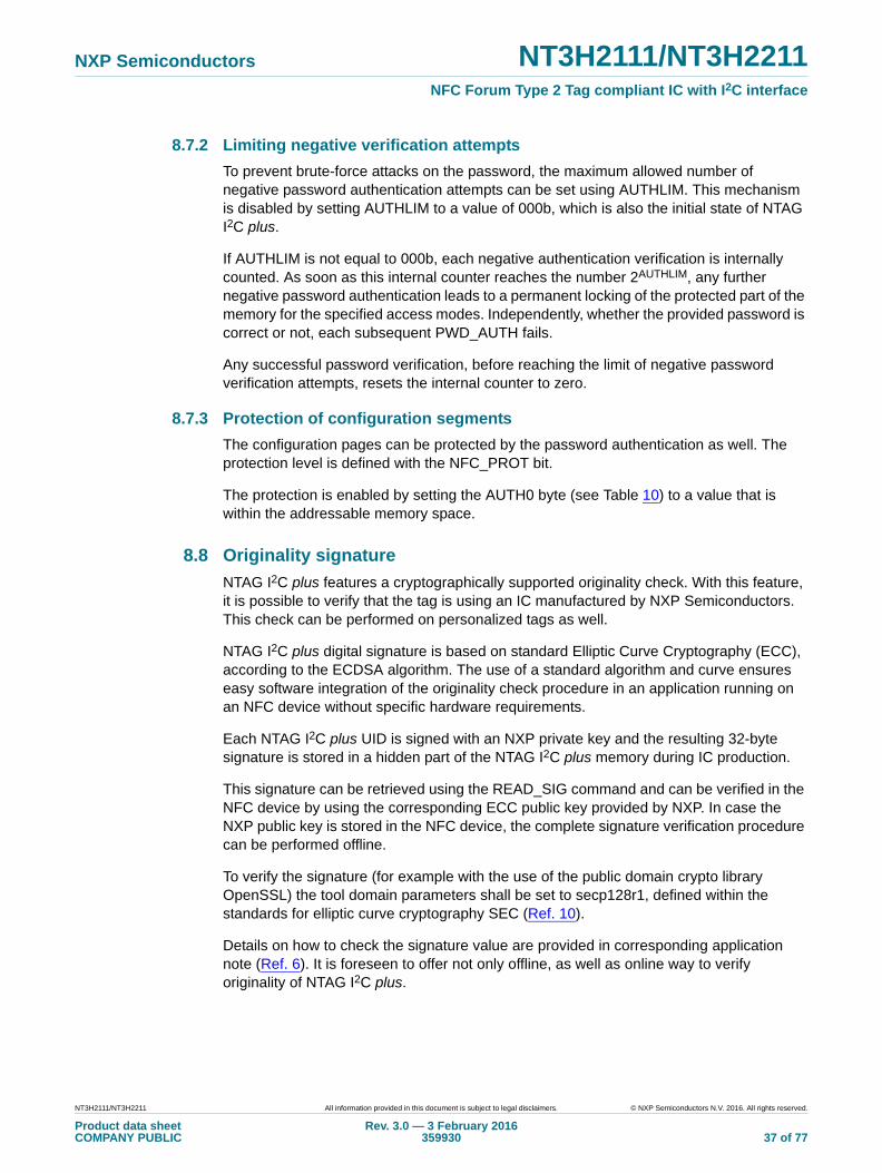
8.7.2 Limiting negative verification attempts
To prevent brute-force attacks on the password, the maximum allowed number of negative password authentication attempts can be set using AUTHLIM. This mechanism is disabled by setting AUTHLIM to a value of 000b, which is also the initial state of NTAG I2C plus.
If AUTHLIM is not equal to 000b, each negative authentication verification is internally counted. As soon as this internal counter reaches the number 2AUTHLIM, any further negative password authentication leads to a permanent locking of the protected part of the memory for the specified access modes. Independently, whether the provided password is correct or not, each subsequent PWD_AUTH fails.
Any successful password verification, before reaching the limit of negative password verification attempts, resets the internal counter to zero.
8.7.3 Protection of configuration segments
The configuration pages can be protected by the password authentication as well. The protection level is defined with the NFC_PROT bit.
The protection is enabled by setting the AUTH0 byte (see Table 10) to a value that is within the addressable memory space.
8.8 Originality signature
NTAG I2C plus features a cryptographically supported originality check. With this feature, it is possible to verify that the tag is using an IC manufactured by NXP Semiconductors. This check can be performed on personalized tags as well.
NTAG I2C plus digital signature is based on standard Elliptic Curve Cryptography (ECC), according to the ECDSA algorithm. The use of a standard algorithm and curve ensures easy software integration of the originality check procedure in an application running on an NFC device without specific hardware requirements.
Each NTAG I2C plus UID is signed with an NXP private key and the resulting 32-byte signature is stored in a hidden part of the NTAG I2C plus memory during IC production.
This signature can be retrieved using the READ_SIG command and can be verified in the NFC device by using the corresponding ECC public key provided by NXP. In case the NXP public key is stored in the NFC device, the complete signature verification procedure can be performed offline.
To verify the signature (for example with the use of the public domain crypto library OpenSSL) the tool domain parameters shall be set to secp128r1, defined within the standards for elliptic curve cryptography SEC (Ref. 10).
Details on how to check the signature value are provided in corresponding application note (Ref. 6). It is foreseen to offer not only offline, as well as online way to verify originality of NTAG I2C plus.
NT3H2111/NT3H2211 All information provided in this document is subject to legal disclaimers. © NXP Semiconductors N.V. 2016. All rights reserved.
Product data sheetCOMPANY PUBLIC
Rev. 3.0 — 3 February 2016359930 37 of 77
NXP Semiconductors NT3H2111/NT3H2211NFC Forum Type 2 Tag compliant IC with I2C interface
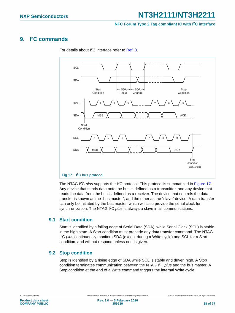
9. I²C commands
For details about I2C interface refer to Ref. 3.
The NTAG I2C plus supports the I2C protocol. This protocol is summarized in Figure 17. Any device that sends data onto the bus is defined as a transmitter, and any device that reads the data from the bus is defined as a receiver. The device that controls the data transfer is known as the “bus master”, and the other as the “slave” device. A data transfer can only be initiated by the bus master, which will also provide the serial clock for synchronization. The NTAG I2C plus is always a slave in all communications.
9.1 Start condition
Start is identified by a falling edge of Serial Data (SDA), while Serial Clock (SCL) is stable in the high state. A Start condition must precede any data transfer command. The NTAG I2C plus continuously monitors SDA (except during a Write cycle) and SCL for a Start condition, and will not respond unless one is given.
9.2 Stop condition
Stop is identified by a rising edge of SDA while SCL is stable and driven high. A Stop condition terminates communication between the NTAG I2C plus and the bus master. A Stop condition at the end of a Write command triggers the internal Write cycle.
Fig 17. I2C bus protocol
SCL
SDA
SCL 1 2 3 7 8 9
1 2 3 7 8 9
ACKMSB
ACKMSB
StartCondition
SDAInput
SDAChange
StopCondition
StopCondition
StartCondition
SDA
SCL
SDA
001aao231
NT3H2111/NT3H2211 All information provided in this document is subject to legal disclaimers. © NXP Semiconductors N.V. 2016. All rights reserved.
Product data sheetCOMPANY PUBLIC
Rev. 3.0 — 3 February 2016359930 38 of 77
NXP Semiconductors NT3H2111/NT3H2211NFC Forum Type 2 Tag compliant IC with I2C interface
9.3 I²C soft reset and NFC silence feature
With the bit NFCS_I2C_RST_ON_OFF (see Table 13) NTAG I2C plus enables two features: a soft reset of the I²C sub-system, and NFC silence, in which the NFC demodulator is disabled.
The I²C soft reset feature interprets an I²C repeated start (no I²C stop in between) as a command to execute a soft reset of the I²C sub-system. This is useful when heavy bus interference can cause the I²C interface to get stuck. A drawback of this feature is that every start symbol then has to be terminated with a Stop, slowing down communication. If a Stop is forgotten, the I²C interface is cleared and previous communication, if any, is lost. Consequently when this feature is used, stop conditions after MEMA for READ/WRITE (see Figure 18) and after REGA for READ/WRITE registers (see Figure 19) shall be send.
The NFC silence feature disables the demodulator. When feature is set, no NFC commands are received, and no replies are issued to commands that were not fully received when NFC Silence was set. This feature allows the tag to “disappear” even if it still is in the reader field. NTAG I2C plus will remain in the ISO state it was in when NFC silence was enabled, until NFC silence is removed.
The combination of these two features in a single bit means that I²C soft reset is only active during NFC silence.
9.4 Acknowledge bit (ACK)
The acknowledge bit is used to indicate a successful byte transfer. The bus transmitter, whether it is the bus master or slave device, releases Serial Data (SDA) after sending eight bits of data. During the ninth clock pulse period, the receiver pulls Serial Data (SDA) low to acknowledge the receipt of the 9th data bits.
9.5 Data input
During data input, the NTAG I2C plus samples SDA on the rising edge of SCL. For correct device operation, SDA must be stable during the rising edge of SCL, and the SDA signal must change only when SCL is driven low.
9.6 Addressing
To start communication between a bus master and the NTAG I2C plus slave device, the bus master must initiate a Start condition. Following this initiation, the bus master sends the device address. The NTAG I2C address from I2C consists of a 7-bit device identifier (see Table 15 for default value).
The 8th bit is the Read/Write bit (RW). This bit is set to 1b for Read and 0b for Write operations.
If a match occurs on the device address, the NTAG I2C plus gives an acknowledgment on SDA during the 9th bit time. If the NTAG I2C plus does not match the device select code, it deselects itself from the bus and clears the register I2C_LOCKED (see Table 12).
Table 15. Default NTAG I2C address from I2C
Device address R/W
b7 b6 b5 b4 b3 b2 b1 b0
Value 1[1] 0[1] 1[1] 0[1] 1 [1] 0 [1] 1 [1] 1/0
NT3H2111/NT3H2211 All information provided in this document is subject to legal disclaimers. © NXP Semiconductors N.V. 2016. All rights reserved.
Product data sheetCOMPANY PUBLIC
Rev. 3.0 — 3 February 2016359930 39 of 77

NXP Semiconductors NT3H2111/NT3H2211NFC Forum Type 2 Tag compliant IC with I2C interface
[1] Initial values - can be changed.
The I2C address of the NTAG I2C (byte 0 - block 0h) can only be modified by the I2C interface. Both interfaces have no READ access to this address and a READ command from the NFC or I²C interface to this byte will only return 04h (manufacturer ID for NXP Semiconductors - see Figure 7).
NT3H2111/NT3H2211 All information provided in this document is subject to legal disclaimers. © NXP Semiconductors N.V. 2016. All rights reserved.
Product data sheetCOMPANY PUBLIC
Rev. 3.0 — 3 February 2016359930 40 of 77

xxxxxxxxxxxxxxxxxxxxx xxxxxxxxxxxxxxxxxxxxxxxxxx xxxxxxx x x x xxxxxxxxxxxxxxxxxxxxxxxxxxxxxx xxxxxxxxxxxxxxxxxxx xx xx xxxxx xxxxxxxxxxxxxxxxxxxxxxxxxxx xxxxxxxxxxxxxxxxxxx xxxxxx xxxxxxxxxxxxxxxxxxxxxxxxxxxxxxxxxxx xxxxxxxxxxxx x x xxxxxxxxxxxxxxxxxxxxx xxxxxxxxxxxxxxxxxxxxxxxxxxxxxx xxxxx xxxxxxxxxxxxxxxxxxxxxxxxxxxxxxxxxxxxxxxxxxxxxxxxxx xxxxxxxx xxxxxxxxxxxxxxxxxxxxxxxxx xxxxxxxxxxxxxxxxxxxx xxx
NT
3H2111
/NT
3H
Pro
du
ct data sh
eetC
OM
PA
NY
PU
BL
ICR
ev. 3.0 — 3 F
ebru
ary 2016359930
41 of 77
NX
P S
emico
nd
ucto
rsN
T3H
2111/NT
3H2211
NF
C F
oru
m Typ
e 2
Tag
co
mp
lian
t IC w
ith I 2C
inte
rfac
e9.7 READ and WRITE Operation
aaa-012811
Stop
D15
A
2211A
ll information
provided in this do
cument is sub
ject to legal d
isclaimers.
© N
XP
Se
micon
ductors N.V
. 2016. All rig
hts reserved.
Fig 18. I2C READ and WRITE operation
7 bits SA and ‘0’Host
Tag
Tag
Start Stop
D0 D1
D0 D1 D15MEMA
A A A
A
A A
A A
7 bits SA and ‘0’Host Start
Write:
Read:
7 bits SA and ‘1’StartStopMEMA
A A
NXP Semiconductors NT3H2111/NT3H2211NFC Forum Type 2 Tag compliant IC with I2C interface
The READ and WRITE operation handle always 16 bytes to be read or written (one block - see Table 6)
For the READ operation (see Figure 18), following a Start condition, the bus master/host sends the NTAG I2C slave address code (SA - 7 bits) with the Read/Write bit (RW) reset to 0. The NTAG I2C plus acknowledges this (A), and waits for one address byte (MEMA), which should correspond to the address of the block of memory (SRAM or EEPROM) that is intended to be read. The NTAG I2C plus responds to a valid address byte with an acknowledge (A). A Stop condition can be then issued. Then the host again issues a start condition followed by the NTAG I2C plus slave address with the Read/Write bit set to 1b. When I2C_CLOCK_STR is set to 0b, a pause of at least 50 s shall be kept before this start condition. The NTAG I2C plus acknowledges this (A) and sends the first byte of data read (D0).The bus master/host acknowledges it (A) and the NTAG I2C plus will subsequently transmit the following 15 bytes of memory read with an acknowledge from the host after every byte. After the last byte of memory data has been transmitted by the NTAG I2C plus, the bus master/host will acknowledge it and issue a Stop condition.
For the WRITE operation (see Figure 18), following a Start condition, the bus master/host sends the NTAG I2C plus slave address code (SA - 7 bits) with the Read/Write bit (RW) reset to 0. The NTAG I2C plus acknowledges this (A), and waits for one address byte (MEMA), which should correspond to the address of the block of memory (SRAM or EEPROM) that is intended to be written. The NTAG I2C plus responds to a valid address byte with an acknowledge (A) and, in the case of a WRITE operation, the bus master/host starts transmitting each 16 bytes (D0...D15) that shall be written at the specified address with an acknowledge of the NTAG I2C plus after each byte (A). After the last byte acknowledge from the NTAG I2C plus, the bus master/host issues a Stop condition.
The memory address accessible via the READ and WRITE operations can only correspond to the EEPROM or SRAM (respectively 00h to 3Ah or F8h to FBh for NTAG I2C plus 1k and 00h to 7Ah or F8h to FBh for NTAG I2C plus 2k).
NT3H2111/NT3H2211 All information provided in this document is subject to legal disclaimers. © NXP Semiconductors N.V. 2016. All rights reserved.
Product data sheetCOMPANY PUBLIC
Rev. 3.0 — 3 February 2016359930 42 of 77

xxxxxxxxxxxxxxxxxxxxx xxxxxxxxxxxxxxxxxxxxxxxxxx xxxxxxx x x x xxxxxxxxxxxxxxxxxxxxxxxxxxxxxx xxxxxxxxxxxxxxxxxxx xx xx xxxxx xxxxxxxxxxxxxxxxxxxxxxxxxxx xxxxxxxxxxxxxxxxxxx xxxxxx xxxxxxxxxxxxxxxxxxxxxxxxxxxxxxxxxxx xxxxxxxxxxxx x x xxxxxxxxxxxxxxxxxxxxx xxxxxxxxxxxxxxxxxxxxxxxxxxxxxx xxxxx xxxxxxxxxxxxxxxxxxxxxxxxxxxxxxxxxxxxxxxxxxxxxxxxxx xxxxxxxx xxxxxxxxxxxxxxxxxxxxxxxxx xxxxxxxxxxxxxxxxxxxx xxx
NT
3H2111
/NT
3H
Pro
du
ct data sh
eetC
OM
PA
NY
PU
BL
ICR
ev. 3.0 — 3 F
ebru
ary 2016359930
43 of 77
NX
P S
emico
nd
ucto
rsN
T3H
2111/NT
3H2211
NF
C F
oru
m Typ
e 2
Tag
co
mp
lian
t IC w
ith I 2C
inte
rfac
e9.8 WRITE and READ register operation
In order to modify or read the session register bytes (see Table 14), NTAG I2C plus requires the WRITE and READ register
aaa-012812
StopA ‘1’
top
REGDATA
2211A
ll information
provided in this do
cument is sub
ject to legal d
isclaimers.
© N
XP
Se
micon
ductors N.V
. 2016. All rig
hts reserved.
operation (see Figure 19).
Fig 19. WRITE and READ register operation
7 bits SA and ‘0’Host
Tag
Tag
Start MEMA REGA
A A
A
7 bits SA and ‘0’Host Start
Write:
Read:
7 bits SA andStartStop
S
MEMA
MASK REGDAT
A
REGA
A A
A A
NXP Semiconductors NT3H2111/NT3H2211NFC Forum Type 2 Tag compliant IC with I2C interface
For the READ register operation, following a Start condition the bus master/host sends the NTAG I2C plus slave address code (SA - 7 bits) with the Read/Write bit (RW) reset to 0. The NTAG I2C plus acknowledges this (A), and waits for one address byte (MEMA) which corresponds to the address of the block of memory with the session register bytes (FEh). The NTAG I2C plus responds to the address byte with an acknowledge (A). Then the bus master/host issues a register address (REGA), which corresponds to the address of the targeted byte inside the block FEh (00h, 01h...to 07h) and then waits for the Stop condition.
Then the bus master/host again issues a start condition followed by the NTAG I2C plus slave address with the Read/Write bit set to 1b. The NTAG I2C plus acknowledges this (A), and sends the selected byte of session register data (REGDAT) within the block FEh. The bus master/host will acknowledge it and issue a Stop condition.
For the WRITE register operation, following a Start condition, the bus master/host sends the NTAG I2C plus slave address code (SA - 7 bits) with the Read/Write bit (RW) reset to 0. The NTAG I2C plus acknowledges this (A), and waits for one address byte (MEMA), which corresponds to the address of the block of memory within the session register bytes (FEh). After the NTAG I2C plus acknowledge (A), the bus master/host issues a register address (REGA), which corresponds to the address of the targeted byte inside the block FEh (00h, 01h...to 07h). After acknowledgement (A) by NTAG I2C plus, the bus master/host issues a MASK byte that defines exactly which bits shall be modified by a 1b bit value at the corresponding bit position. Following the NTAG I2C plus acknowledge (A), the new register data (one byte - REGDAT) to be written is transmitted by the bus master/host. The NTAG I2C plus acknowledges it (A), and the bus master/host issues a stop condition.
NT3H2111/NT3H2211 All information provided in this document is subject to legal disclaimers. © NXP Semiconductors N.V. 2016. All rights reserved.
Product data sheetCOMPANY PUBLIC
Rev. 3.0 — 3 February 2016359930 44 of 77
NXP Semiconductors NT3H2111/NT3H2211NFC Forum Type 2 Tag compliant IC with I2C interface
10. NFC Command
NTAG activation follows the ISO/IEC 14443-3 Type A specification. After NTAG I2C plus has been selected, it can either be deactivated using the ISO/IEC 14443 HALT command, or NTAG commands (e.g. READ_SIG, PWD_AUTH, SECTOR_SELECT, READ or WRITE) can be performed. For more details about the card activation refer to Ref. 2.
10.1 NTAG I2C plus command overview
All available commands for NTAG I2C plus are shown in Table 16.
[1] Unless otherwise specified, all commands use the coding and framing as described in Ref. 1.
10.2 Timing
The command and response timing shown in this document are not to scale and values are rounded to 1 s.
All given command and response times refer to the data frames, including start of communication and end of communication. They do not include the encoding (like the Miller pulses). An NFC device data frame contains the start of communication (1 “start bit”) and the end of communication (one logic 0 + 1-bit length of unmodulated carrier). An NFC tag data frame contains the start of communication (1 “start bit”) and the end of communication (1-bit length of no subcarrier).
The minimum command response time is specified according to Ref. 1 as an integer n, which specifies the NFC device to NFC tag frame delay time. The frame delay time from NFC tag to NFC device is at least 87 s. The maximum command response time is specified as a time-out value. Depending on the command, the TACK value specified for command responses defines the NFC device to NFC tag frame delay time. It does it for either the 4-bit ACK value specified or for a data frame.
Table 16. Command overview
Command[1] ISO/IEC 14443 NFC FORUM Command code (hexadecimal)
Request REQA SENS_REQ 26h (7 bit)
Wake-up WUPA ALL_REQ 52h (7 bit)
Anticollision CL1 Anticollision CL1 SDD_REQ CL1 93h 20h
Select CL1 Select CL1 SEL_REQ CL1 93h 70h
Anticollision CL2 Anticollision CL2 SDD_REQ CL2 95h 20h
Select CL2 Select CL2 SEL_REQ CL2 95h 70h
Halt HLTA SLP_REQ 50h 00h
GET_VERSION - - 60h
READ - READ 30h
FAST_READ - - 3Ah
WRITE - WRITE A2h
FAST_WRITE - - A6h
SECTOR_SELECT - SECTOR_SELECT C2h
PWD_AUTH - - 1Bh
READ_SIG - - 3Ch
NT3H2111/NT3H2211 All information provided in this document is subject to legal disclaimers. © NXP Semiconductors N.V. 2016. All rights reserved.
Product data sheetCOMPANY PUBLIC
Rev. 3.0 — 3 February 2016359930 45 of 77
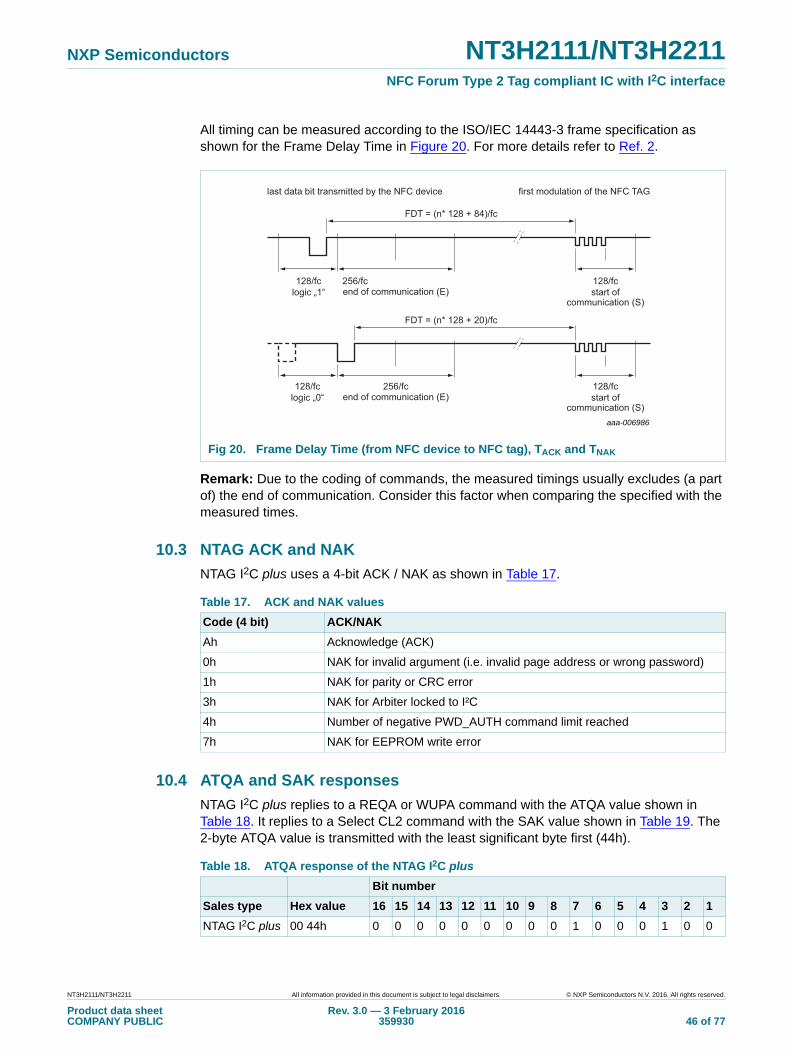
NXP Semiconductors NT3H2111/NT3H2211NFC Forum Type 2 Tag compliant IC with I2C interface
All timing can be measured according to the ISO/IEC 14443-3 frame specification as shown for the Frame Delay Time in Figure 20. For more details refer to Ref. 2.
Remark: Due to the coding of commands, the measured timings usually excludes (a part of) the end of communication. Consider this factor when comparing the specified with the measured times.
10.3 NTAG ACK and NAK
NTAG I2C plus uses a 4-bit ACK / NAK as shown in Table 17.
10.4 ATQA and SAK responses
NTAG I2C plus replies to a REQA or WUPA command with the ATQA value shown in Table 18. It replies to a Select CL2 command with the SAK value shown in Table 19. The 2-byte ATQA value is transmitted with the least significant byte first (44h).
Fig 20. Frame Delay Time (from NFC device to NFC tag), TACK and TNAK
last data bit transmitted by the NFC device
FDT = (n* 128 + 84)/fc
first modulation of the NFC TAG
FDT = (n* 128 + 20)/fc
aaa-006986
128/fc logic „1“
128/fc logic „0“
256/fcend of communication (E)
256/fcend of communication (E)
128/fc start of
communication (S)
communication (S)
128/fc start of
Table 17. ACK and NAK values
Code (4 bit) ACK/NAK
Ah Acknowledge (ACK)
0h NAK for invalid argument (i.e. invalid page address or wrong password)
1h NAK for parity or CRC error
3h NAK for Arbiter locked to I²C
4h Number of negative PWD_AUTH command limit reached
7h NAK for EEPROM write error
Table 18. ATQA response of the NTAG I2C plus
Bit number
Sales type Hex value 16 15 14 13 12 11 10 9 8 7 6 5 4 3 2 1
NTAG I2C plus 00 44h 0 0 0 0 0 0 0 0 0 1 0 0 0 1 0 0
NT3H2111/NT3H2211 All information provided in this document is subject to legal disclaimers. © NXP Semiconductors N.V. 2016. All rights reserved.
Product data sheetCOMPANY PUBLIC
Rev. 3.0 — 3 February 2016359930 46 of 77
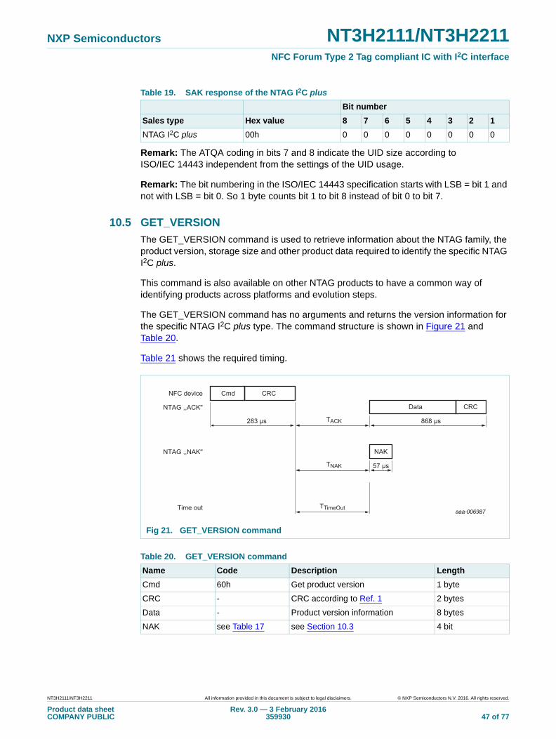
NXP Semiconductors NT3H2111/NT3H2211NFC Forum Type 2 Tag compliant IC with I2C interface
Remark: The ATQA coding in bits 7 and 8 indicate the UID size according to ISO/IEC 14443 independent from the settings of the UID usage.
Remark: The bit numbering in the ISO/IEC 14443 specification starts with LSB = bit 1 and not with LSB = bit 0. So 1 byte counts bit 1 to bit 8 instead of bit 0 to bit 7.
10.5 GET_VERSION
The GET_VERSION command is used to retrieve information about the NTAG family, the product version, storage size and other product data required to identify the specific NTAG I2C plus.
This command is also available on other NTAG products to have a common way of identifying products across platforms and evolution steps.
The GET_VERSION command has no arguments and returns the version information for the specific NTAG I2C plus type. The command structure is shown in Figure 21 and Table 20.
Table 21 shows the required timing.
Table 19. SAK response of the NTAG I2C plus
Bit number
Sales type Hex value 8 7 6 5 4 3 2 1
NTAG I2C plus 00h 0 0 0 0 0 0 0 0
Fig 21. GET_VERSION command
Table 20. GET_VERSION command
Name Code Description Length
Cmd 60h Get product version 1 byte
CRC - CRC according to Ref. 1 2 bytes
Data - Product version information 8 bytes
NAK see Table 17 see Section 10.3 4 bit
CRC
CRC
NFC device Cmd
DataNTAG ,,ACK''
283 μs 868 μs
NTAG ,,NAK'' NAK
Time out TTimeOut
TNAK
TACK
57 μs
aaa-006987
NT3H2111/NT3H2211 All information provided in this document is subject to legal disclaimers. © NXP Semiconductors N.V. 2016. All rights reserved.
Product data sheetCOMPANY PUBLIC
Rev. 3.0 — 3 February 2016359930 47 of 77
NXP Semiconductors NT3H2111/NT3H2211NFC Forum Type 2 Tag compliant IC with I2C interface
[1] Refer to Section 10.2 “Timing”.
The most significant 7 bits of the storage size byte are interpreted as an unsigned integer value n. As a result, it codes the total available user memory size as 2n. If the least significant bit is 0b, the user memory size is exactly 2n. If the least significant bit is 1b, the user memory size is between 2n and 2n+1.
The user memory for NTAG I2C plus 1k is 888 bytes. This memory size is between 512 bytes and 1024 bytes. Therefore, the most significant 7 bits of the value 13h are 0001001b, which means n = 9, and the least significant bit is 1b.
The user memory for NTAG I2C plus 2k is 1912 bytes. This memory size is between 1024 bytes and 2048 bytes. Therefore, the most significant 7 bits of the value 15h are 0001010b, which means n = 10, and the least significant bit is 1b.
10.6 READ_SIG
The READ_SIG command returns an IC specific, 32-byte ECC signature, to verify NXPSemiconductors as the silicon vendor. The signature is programmed at chip production and cannot be changed afterwards. The command structure is shown in Figure 24 and Table 27.
Table 28 shows the required timing.
Table 21. GET_VERSION timingThese times exclude the end of communication of the NFC device.
TACK/NAK min TACK/NAK max TTimeOut
GET_VERSION n=9[1] TTimeOut 5 ms
Table 22. GET_VERSION response for NTAG I2C plus 1k and 2k
Byte no.
Description NTAG I2C plus 1k
NTAG I2C plus 2k
Interpretation
0 fixed Header 00h 00h
1 vendor ID 04h 04h NXP Semiconductors
2 product type 04h 04h NTAG
3 product subtype 05h 05h 50 pF I2C, Field detection
4 major product version 02h 02h 2
5 minor product version 02h 02h V2
6 storage size 13h 15h see following information
7 protocol type 03h 03h ISO/IEC 14443-3 compliant
NT3H2111/NT3H2211 All information provided in this document is subject to legal disclaimers. © NXP Semiconductors N.V. 2016. All rights reserved.
Product data sheetCOMPANY PUBLIC
Rev. 3.0 — 3 February 2016359930 48 of 77
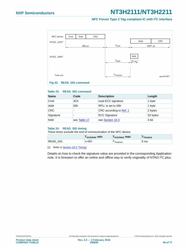
NXP Semiconductors NT3H2111/NT3H2211NFC Forum Type 2 Tag compliant IC with I2C interface
[1] Refer to Section 10.2 “Timing”.
Details on how to check the signature value are provided in the corresponding Application note. It is foreseen to offer an online and offline way to verify originality of NTAG I2C plus.
Fig 22. READ_SIG command
Table 23. READ_SIG command
Name Code Description Length
Cmd 3Ch read ECC signature 1 byte
Addr 00h RFU, is set to 00h 1 byte
CRC - CRC according to Ref. 1 2 bytes
Signature - ECC Signature 32 bytes
NAK see Table 17 see Section 10.3 4 bit
Table 24. READ_SIG timingThese times exclude the end of communication of the NFC device.
TACK/NAK min TACK/NAK max TTimeOut
READ_SIG n=9[1] TTimeOut 5 ms
CRC
CRC
AddrNFC device Cmd
DataNTAG ,,ACK''
368 μs 2907 μs
NTAG ,,NAK'' NAK
Time out TTimeOut
TNAK
TACK
57 μs
aaa-021657
NT3H2111/NT3H2211 All information provided in this document is subject to legal disclaimers. © NXP Semiconductors N.V. 2016. All rights reserved.
Product data sheetCOMPANY PUBLIC
Rev. 3.0 — 3 February 2016359930 49 of 77
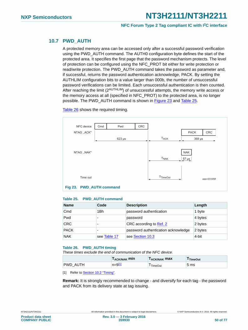
NXP Semiconductors NT3H2111/NT3H2211NFC Forum Type 2 Tag compliant IC with I2C interface
10.7 PWD_AUTH
A protected memory area can be accessed only after a successful password verification using the PWD_AUTH command. The AUTH0 configuration byte defines the start of the protected area. It specifies the first page that the password mechanism protects. The level of protection can be configured using the NFC_PROT bit either for write protection or read/write protection. The PWD_AUTH command takes the password as parameter and, if successful, returns the password authentication acknowledge, PACK. By setting the AUTHLIM configuration bits to a value larger than 000b, the number of unsuccessful password verifications can be limited. Each unsuccessful authentication is then counted. After reaching the limit (2AUTHLIM) of unsuccessful attempts, the memory write access or the memory access at all (specified in NFC_PROT) to the protected area, is no longer possible. The PWD_AUTH command is shown in Figure 23 and Table 25.
Table 26 shows the required timing.
[1] Refer to Section 10.2 “Timing”.
Remark: It is strongly recommended to change - and diversify for each tag - the password and PACK from its delivery state at tag issuing.
Fig 23. PWD_AUTH command
Table 25. PWD_AUTH command
Name Code Description Length
Cmd 1Bh password authentication 1 byte
Pwd - password 4 bytes
CRC - CRC according to Ref. 2 2 bytes
PACK - password authentication acknowledge 2 bytes
NAK see Table 17 see Section 10.3 4-bit
Table 26. PWD_AUTH timingThese times exclude the end of communication of the NFC device.
TACK/NAK min TACK/NAK max TTimeOut
PWD_AUTH n=9[1] TTimeOut 5 ms
CRC
CRC
NFC device Cmd
NTAG ,,ACK''
623 μs
NTAG ,,NAK'' NAK
Time out TTimeOut
TNAK
TACK
57 μs
PACK
368 μs
Pwd
aaa-021658
NT3H2111/NT3H2211 All information provided in this document is subject to legal disclaimers. © NXP Semiconductors N.V. 2016. All rights reserved.
Product data sheetCOMPANY PUBLIC
Rev. 3.0 — 3 February 2016359930 50 of 77
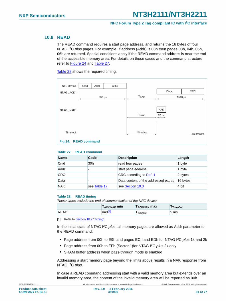
NXP Semiconductors NT3H2111/NT3H2211NFC Forum Type 2 Tag compliant IC with I2C interface
10.8 READ
The READ command requires a start page address, and returns the 16 bytes of four NTAG I2C plus pages. For example, if address (Addr) is 03h then pages 03h, 04h, 05h, 06h are returned. Special conditions apply if the READ command address is near the end of the accessible memory area. For details on those cases and the command structure refer to Figure 24 and Table 27.
Table 28 shows the required timing.
[1] Refer to Section 10.2 “Timing”.
In the initial state of NTAG I2C plus, all memory pages are allowed as Addr parameter to the READ command:
• Page address from 00h to E9h and pages ECh and EDh for NTAG I2C plus 1k and 2k
• Page address from 00h to FFh (Sector 1)for NTAG I2C plus 2k only
• SRAM buffer address when pass-through mode is enabled
Addressing a start memory page beyond the limits above results in a NAK response from NTAG I2C plus.
In case a READ command addressing start with a valid memory area but extends over an invalid memory area, the content of the invalid memory area will be reported as 00h.
Fig 24. READ command
Table 27. READ command
Name Code Description Length
Cmd 30h read four pages 1 byte
Addr - start page address 1 byte
CRC - CRC according to Ref. 1 2 bytes
Data - Data content of the addressed pages 16 bytes
NAK see Table 17 see Section 10.3 4 bit
Table 28. READ timingThese times exclude the end of communication of the NFC device.
TACK/NAK min TACK/NAK max TTimeOut
READ n=9[1] TTimeOut 5 ms
CRC
CRC
AddrNFC device Cmd
DataNTAG ,,ACK''
368 μs 1548 μs
NTAG ,,NAK'' NAK
Time out TTimeOut
TNAK
TACK
57 μs
aaa-006988
NT3H2111/NT3H2211 All information provided in this document is subject to legal disclaimers. © NXP Semiconductors N.V. 2016. All rights reserved.
Product data sheetCOMPANY PUBLIC
Rev. 3.0 — 3 February 2016359930 51 of 77
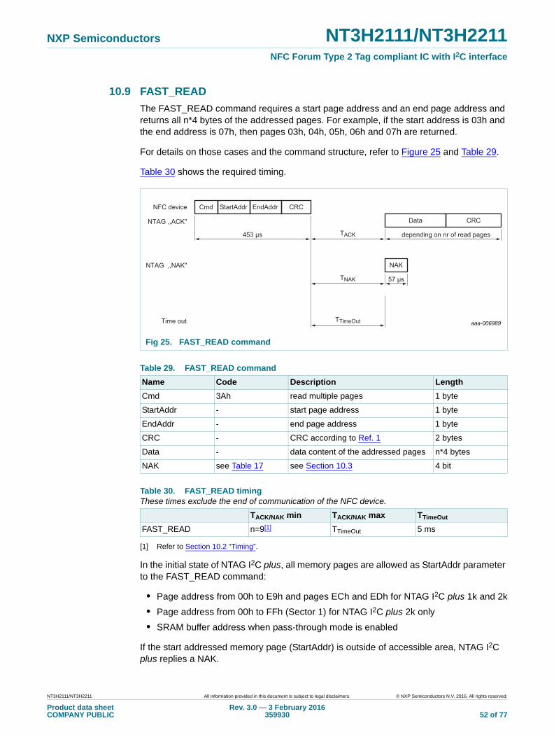
NXP Semiconductors NT3H2111/NT3H2211NFC Forum Type 2 Tag compliant IC with I2C interface
10.9 FAST_READ
The FAST_READ command requires a start page address and an end page address and returns all n*4 bytes of the addressed pages. For example, if the start address is 03h and the end address is 07h, then pages 03h, 04h, 05h, 06h and 07h are returned.
For details on those cases and the command structure, refer to Figure 25 and Table 29.
Table 30 shows the required timing.
[1] Refer to Section 10.2 “Timing”.
In the initial state of NTAG I2C plus, all memory pages are allowed as StartAddr parameter to the FAST_READ command:
• Page address from 00h to E9h and pages ECh and EDh for NTAG I2C plus 1k and 2k
• Page address from 00h to FFh (Sector 1) for NTAG I2C plus 2k only
• SRAM buffer address when pass-through mode is enabled
If the start addressed memory page (StartAddr) is outside of accessible area, NTAG I2C plus replies a NAK.
Fig 25. FAST_READ command
Table 29. FAST_READ command
Name Code Description Length
Cmd 3Ah read multiple pages 1 byte
StartAddr - start page address 1 byte
EndAddr - end page address 1 byte
CRC - CRC according to Ref. 1 2 bytes
Data - data content of the addressed pages n*4 bytes
NAK see Table 17 see Section 10.3 4 bit
Table 30. FAST_READ timingThese times exclude the end of communication of the NFC device.
TACK/NAK min TACK/NAK max TTimeOut
FAST_READ n=9[1] TTimeOut 5 ms
CRC
CRC
StartAddrNFC device Cmd
DataNTAG ,,ACK''
453 μs depending on nr of read pages
NTAG ,,NAK'' NAK
Time out TTimeOut
TNAK
TACK
57 μs
EndAddr
aaa-006989
NT3H2111/NT3H2211 All information provided in this document is subject to legal disclaimers. © NXP Semiconductors N.V. 2016. All rights reserved.
Product data sheetCOMPANY PUBLIC
Rev. 3.0 — 3 February 2016359930 52 of 77
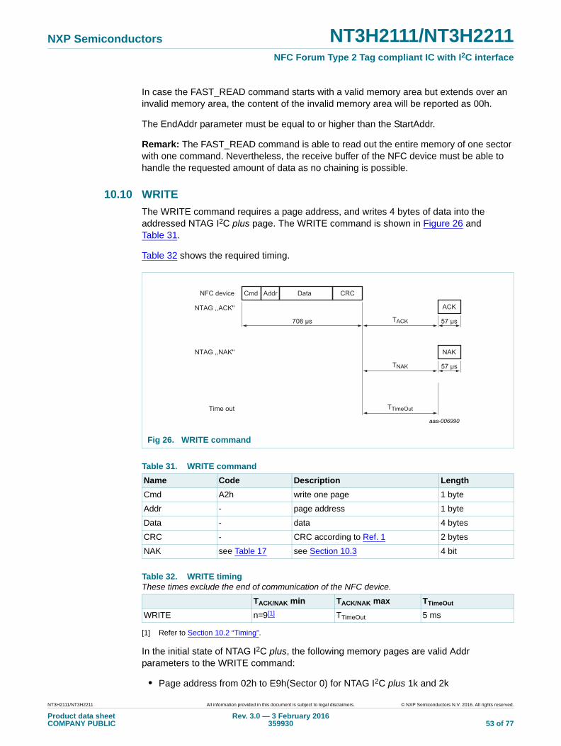
NXP Semiconductors NT3H2111/NT3H2211NFC Forum Type 2 Tag compliant IC with I2C interface
In case the FAST_READ command starts with a valid memory area but extends over an invalid memory area, the content of the invalid memory area will be reported as 00h.
The EndAddr parameter must be equal to or higher than the StartAddr.
Remark: The FAST_READ command is able to read out the entire memory of one sector with one command. Nevertheless, the receive buffer of the NFC device must be able to handle the requested amount of data as no chaining is possible.
10.10 WRITE
The WRITE command requires a page address, and writes 4 bytes of data into the addressed NTAG I2C plus page. The WRITE command is shown in Figure 26 and Table 31.
Table 32 shows the required timing.
[1] Refer to Section 10.2 “Timing”.
In the initial state of NTAG I2C plus, the following memory pages are valid Addr parameters to the WRITE command:
• Page address from 02h to E9h(Sector 0) for NTAG I2C plus 1k and 2k
Fig 26. WRITE command
Table 31. WRITE command
Name Code Description Length
Cmd A2h write one page 1 byte
Addr - page address 1 byte
Data - data 4 bytes
CRC - CRC according to Ref. 1 2 bytes
NAK see Table 17 see Section 10.3 4 bit
Table 32. WRITE timingThese times exclude the end of communication of the NFC device.
TACK/NAK min TACK/NAK max TTimeOut
WRITE n=9[1] TTimeOut 5 ms
CRCAddrNFC device Cmd
NTAG ,,ACK''
708 μs
NTAG ,,NAK'' NAK
Time out TTimeOut
TNAK
TACK
57 μs
ACK
57 μs
Data
aaa-006990
NT3H2111/NT3H2211 All information provided in this document is subject to legal disclaimers. © NXP Semiconductors N.V. 2016. All rights reserved.
Product data sheetCOMPANY PUBLIC
Rev. 3.0 — 3 February 2016359930 53 of 77
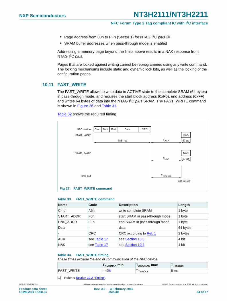
NXP Semiconductors NT3H2111/NT3H2211NFC Forum Type 2 Tag compliant IC with I2C interface
• Page address from 00h to FFh (Sector 1) for NTAG I2C plus 2k
• SRAM buffer addresses when pass-through mode is enabled
Addressing a memory page beyond the limits above results in a NAK response from NTAG I2C plus.
Pages that are locked against writing cannot be reprogrammed using any write command. The locking mechanisms include static and dynamic lock bits, as well as the locking of the configuration pages.
10.11 FAST_WRITE
The FAST_WRITE allows to write data in ACTIVE state to the complete SRAM (64 bytes) in pass-through mode, and requires the start block address (0xF0), end address (0xFF) and writes 64 bytes of data into the NTAG I2C plus SRAM. The FAST_WRITE command is shown in Figure 26 and Table 31.
Table 32 shows the required timing.
[1] Refer to Section 10.2 “Timing”.
Fig 27. FAST_WRITE command
Table 33. FAST_WRITE command
Name Code Description Length
Cmd A6h write complete SRAM 1 byte
START_ADDR F0h start SRAM in pass-through mode 1 byte
END_ADDR FFh end SRAM in pass-through mode 1 byte
Data - data 64 bytes
- CRC CRC according to Ref. 1 2 bytes
ACK see Table 17 see Section 10.3 4 bit
NAK see Table 17 see Section 10.3 4 bit
Table 34. FAST_WRITE timingThese times exclude the end of communication of the NFC device.
TACK/NAK min TACK/NAK max TTimeOut
FAST_WRITE n=9[1] TTimeOut 5 ms
CRCStart EndNFC device Cmd
NTAG ,,ACK''
5881 μs
NTAG ,,NAK'' NAK
Time out TTimeOut
TNAK
TACK
57 μs
ACK
57 μs
Data
aaa-021659
NT3H2111/NT3H2211 All information provided in this document is subject to legal disclaimers. © NXP Semiconductors N.V. 2016. All rights reserved.
Product data sheetCOMPANY PUBLIC
Rev. 3.0 — 3 February 2016359930 54 of 77
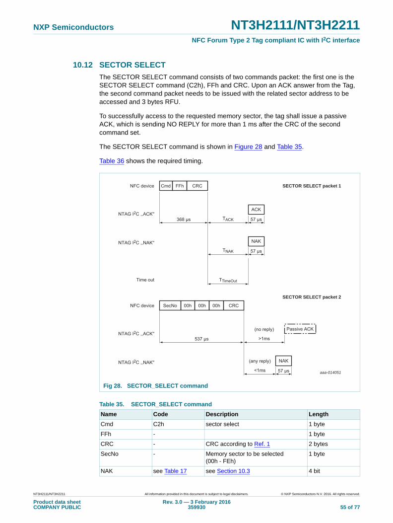
NXP Semiconductors NT3H2111/NT3H2211NFC Forum Type 2 Tag compliant IC with I2C interface
10.12 SECTOR SELECT
The SECTOR SELECT command consists of two commands packet: the first one is the SECTOR SELECT command (C2h), FFh and CRC. Upon an ACK answer from the Tag, the second command packet needs to be issued with the related sector address to be accessed and 3 bytes RFU.
To successfully access to the requested memory sector, the tag shall issue a passive ACK, which is sending NO REPLY for more than 1 ms after the CRC of the second command set.
The SECTOR SELECT command is shown in Figure 28 and Table 35.
Table 36 shows the required timing.
Fig 28. SECTOR_SELECT command
Table 35. SECTOR_SELECT command
Name Code Description Length
Cmd C2h sector select 1 byte
FFh - 1 byte
CRC - CRC according to Ref. 1 2 bytes
SecNo - Memory sector to be selected (00h - FEh)
1 byte
NAK see Table 17 see Section 10.3 4 bit
aaa-014051
CRCFFhNFC device Cmd
SecNo 00h 00h 00h CRC
368 μs
NTAG I2C ,,NAK''
NTAG I2C ,,ACK''
NTAG I2C ,,NAK''
NTAG I2C ,,ACK''
NAK
Time out
NFC device
TTimeOut
TNAK
TACK
57 μs
ACK
57 μs
NAK
<1ms
>1ms537 μs
57 μs
Passive ACK
SECTOR SELECT packet 2
SECTOR SELECT packet 1
(any reply)
(no reply)
NT3H2111/NT3H2211 All information provided in this document is subject to legal disclaimers. © NXP Semiconductors N.V. 2016. All rights reserved.
Product data sheetCOMPANY PUBLIC
Rev. 3.0 — 3 February 2016359930 55 of 77
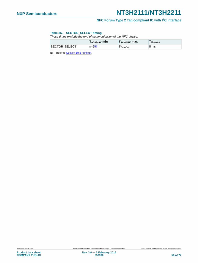
NXP Semiconductors NT3H2111/NT3H2211NFC Forum Type 2 Tag compliant IC with I2C interface
[1] Refer to Section 10.2 “Timing”.
Table 36. SECTOR_SELECT timingThese times exclude the end of communication of the NFC device.
TACK/NAK min TACK/NAK max TTimeOut
SECTOR_SELECT n=9[1] TTimeOut 5 ms
NT3H2111/NT3H2211 All information provided in this document is subject to legal disclaimers. © NXP Semiconductors N.V. 2016. All rights reserved.
Product data sheetCOMPANY PUBLIC
Rev. 3.0 — 3 February 2016359930 56 of 77
NXP Semiconductors NT3H2111/NT3H2211NFC Forum Type 2 Tag compliant IC with I2C interface
11. Communication and arbitration between NFC and I²C interface
If both interfaces are powered by their corresponding source, only one interface shall have access to the memory according to the "first-come, first-serve" principle.
In NS_REG, the two status bits I2C_LOCKED and RF_LOCKED reflect the status of the NTAG I2C plus memory access and indicate which interface is locking the memory access. At power-on, both bits are 0, setting the arbitration in idle mode.
In the case arbiter locks to the I²C interface, an NFC device still can read the session registers. If the NFC state machine is in ACTIVE state, only the SECTOR SELECT command is allowed. But any other command requiring EEPROM access like READ or WRITE is handled as an illegal command and replied to with a special NAK value.
In the case where the memory access is locked to the NFC interface, the I²C host still can access the session register, by issuing a 'Register READ/WRITE' command. All other read or write commands will be replied to with a NACK to the I²C host.
11.1 Pass-through mode not activated
PTHRU_ON_OFF = 0b (see Table 14) indicates non-pass-through mode.
11.1.1 I²C interface access
If the tag is in the IDLE or HALT state (NFC state after POR or HALT-command) and the correct I²C slave address of NTAG I2C plus is received following the START condition, the bit I2C_LOCKED will be automatically set to 1b. If I2C_LOCKED = 1b, the I²C interface has access to the tag memory and the tag will respond with a NACK to any memory READ/WRITE command on the NFC interface other than reading the session register bytes command during this time.
I2C_LOCKED must be either reset to 0b at the end of the I²C sequence or will be cleared automatically after the end of the watch dog timer.
11.1.2 NFC interface access
The arbitration will allow the NFC interface read and write accesses to EEPROM only when I2C_LOCKED is set to 0b.
RF_LOCKED is automatically set to 1b if the tag receives a valid command (EEPROM Access Commands) on the NFC interface. If RF_LOCKED = 1b, the tag is locked to the NFC interface and will not respond to any command from the I²C interface other than READ register command (see Table 14).
RF_LOCKED is automatically set to 0b in one of the following conditions
• At POR or if the NFC field is switched off
• If the tag is set to the HALT state with a HALT command on the NFC interface
• If the memory access command is finished on the NFC interface
When the NFC interface has read the last page of the NDEF message specified in LAST_NDEF_BLOCK (see Table 13 and Table 14) the bit NDEF_DATA_READ - in the register NS_REG see Table 14 - is set to 1b and indicates to the I²C interface that, for example, new NDEF data can be written.
NT3H2111/NT3H2211 All information provided in this document is subject to legal disclaimers. © NXP Semiconductors N.V. 2016. All rights reserved.
Product data sheetCOMPANY PUBLIC
Rev. 3.0 — 3 February 2016359930 57 of 77
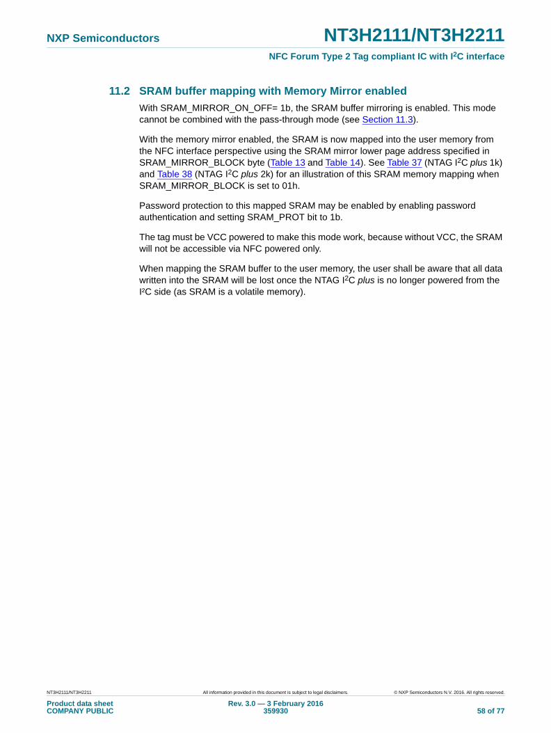
NXP Semiconductors NT3H2111/NT3H2211NFC Forum Type 2 Tag compliant IC with I2C interface
11.2 SRAM buffer mapping with Memory Mirror enabled
With SRAM_MIRROR_ON_OFF= 1b, the SRAM buffer mirroring is enabled. This mode cannot be combined with the pass-through mode (see Section 11.3).
With the memory mirror enabled, the SRAM is now mapped into the user memory from the NFC interface perspective using the SRAM mirror lower page address specified in SRAM_MIRROR_BLOCK byte (Table 13 and Table 14). See Table 37 (NTAG I2C plus 1k) and Table 38 (NTAG I2C plus 2k) for an illustration of this SRAM memory mapping when SRAM_MIRROR_BLOCK is set to 01h.
Password protection to this mapped SRAM may be enabled by enabling password authentication and setting SRAM_PROT bit to 1b.
The tag must be VCC powered to make this mode work, because without VCC, the SRAM will not be accessible via NFC powered only.
When mapping the SRAM buffer to the user memory, the user shall be aware that all data written into the SRAM will be lost once the NTAG I2C plus is no longer powered from the I²C side (as SRAM is a volatile memory).
NT3H2111/NT3H2211 All information provided in this document is subject to legal disclaimers. © NXP Semiconductors N.V. 2016. All rights reserved.
Product data sheetCOMPANY PUBLIC
Rev. 3.0 — 3 February 2016359930 58 of 77
NXP Semiconductors NT3H2111/NT3H2211NFC Forum Type 2 Tag compliant IC with I2C interface
Table 37. Illustration of the SRAM memory addressing via the NFC interface (with SRAM_MIRROR_ON_OFF set to 1b and SRAM_MIRROR_BLOCK set to 01h) for the NTAG I2C plus 1k
Sectoraddress
Page address Byte number within a page Access cond.ACTIVE state
Access cond. AUTH. stateDec. Hex. 0 1 2 3
0 0 00h Serial number READ
1 01h Serial number Internal READ
2 02h Internal Static lock bytes READ/R&W
3 03h Capability Container (CC) READ&WRITE
4 04h
SRAM READ&WRITE... ...
19 13h
... ... Unprotected user memory READ&WRITE
AUTH0 AUTH0
Protected user memory READ READ&WRITE... ...
225 E1h
226 E2h Dynamic lock bytes 00h R&W/READ
227 E3h RFU RFU RFU AUTH0 READ READ&WRITE
228 E4h ACCESS RFU RFU RFU READ READ&WRITE
229 E5h PWD READ READ&WRITE
230 E6h PACK RFU RFU READ READ&WRITE
231 E7h PT_I2C RFU RFU RFU READ READ&WRITE
232 E8hConfiguration registers see 8.3.12
233 E9h
234 EAhInvalid access - returns NAK n.a.
235 EBh
236 EChSession registers see 8.3.12
237 EDh
238 EEhInvalid access - returns NAK n.a.
239 EFh
240 F0h
Invalid access - returns NAK n.a.... ...
255 FFh
1 ... ... Invalid access - returns NAK n.a.
2 ... ... Invalid access - returns NAK n.a.
3 0 00hInvalid access - returns NAK n.a.
... ...
248 F8hSession registers see 8.3.12
249 F9h
... ...Invalid access - returns NAK n.a.
255 FFh
NT3H2111/NT3H2211 All information provided in this document is subject to legal disclaimers. © NXP Semiconductors N.V. 2016. All rights reserved.
Product data sheetCOMPANY PUBLIC
Rev. 3.0 — 3 February 2016359930 59 of 77
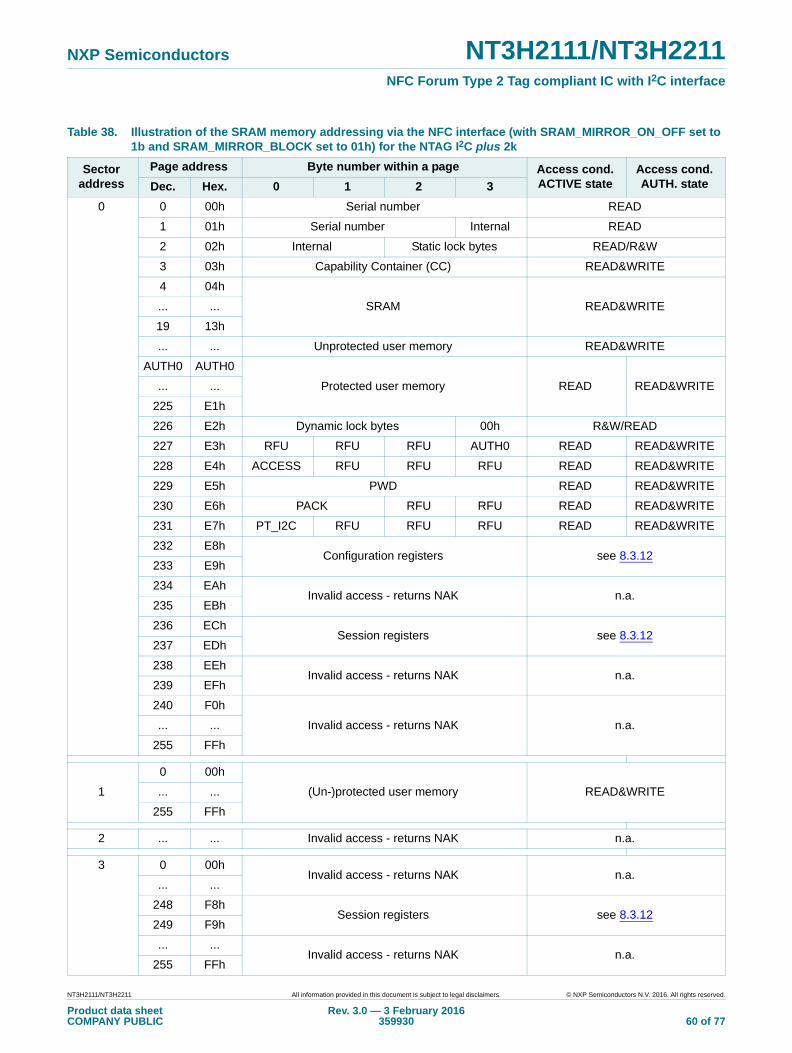
NXP Semiconductors NT3H2111/NT3H2211NFC Forum Type 2 Tag compliant IC with I2C interface
Table 38. Illustration of the SRAM memory addressing via the NFC interface (with SRAM_MIRROR_ON_OFF set to 1b and SRAM_MIRROR_BLOCK set to 01h) for the NTAG I2C plus 2k
Sectoraddress
Page address Byte number within a page Access cond.ACTIVE state
Access cond. AUTH. stateDec. Hex. 0 1 2 3
0 0 00h Serial number READ
1 01h Serial number Internal READ
2 02h Internal Static lock bytes READ/R&W
3 03h Capability Container (CC) READ&WRITE
4 04h
SRAM READ&WRITE... ...
19 13h
... ... Unprotected user memory READ&WRITE
AUTH0 AUTH0
Protected user memory READ READ&WRITE... ...
225 E1h
226 E2h Dynamic lock bytes 00h R&W/READ
227 E3h RFU RFU RFU AUTH0 READ READ&WRITE
228 E4h ACCESS RFU RFU RFU READ READ&WRITE
229 E5h PWD READ READ&WRITE
230 E6h PACK RFU RFU READ READ&WRITE
231 E7h PT_I2C RFU RFU RFU READ READ&WRITE
232 E8hConfiguration registers see 8.3.12
233 E9h
234 EAhInvalid access - returns NAK n.a.
235 EBh
236 EChSession registers see 8.3.12
237 EDh
238 EEhInvalid access - returns NAK n.a.
239 EFh
240 F0h
Invalid access - returns NAK n.a.... ...
255 FFh
1
0 00h
(Un-)protected user memory READ&WRITE... ...
255 FFh
2 ... ... Invalid access - returns NAK n.a.
3 0 00hInvalid access - returns NAK n.a.
... ...
248 F8hSession registers see 8.3.12
249 F9h
... ...Invalid access - returns NAK n.a.
255 FFh
NT3H2111/NT3H2211 All information provided in this document is subject to legal disclaimers. © NXP Semiconductors N.V. 2016. All rights reserved.
Product data sheetCOMPANY PUBLIC
Rev. 3.0 — 3 February 2016359930 60 of 77
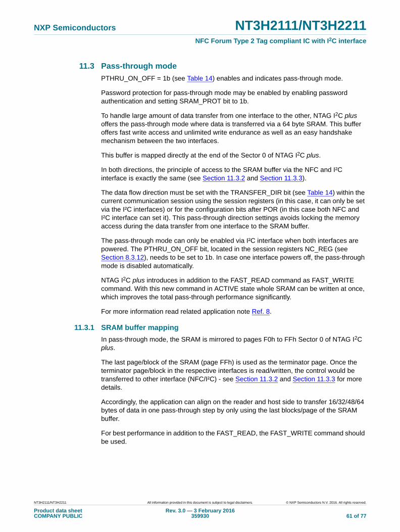
NXP Semiconductors NT3H2111/NT3H2211NFC Forum Type 2 Tag compliant IC with I2C interface
11.3 Pass-through mode
PTHRU_ON_OFF = 1b (see Table 14) enables and indicates pass-through mode.
Password protection for pass-through mode may be enabled by enabling password authentication and setting SRAM_PROT bit to 1b.
To handle large amount of data transfer from one interface to the other, NTAG I2C plus offers the pass-through mode where data is transferred via a 64 byte SRAM. This buffer offers fast write access and unlimited write endurance as well as an easy handshake mechanism between the two interfaces.
This buffer is mapped directly at the end of the Sector 0 of NTAG I2C plus.
In both directions, the principle of access to the SRAM buffer via the NFC and I²C interface is exactly the same (see Section 11.3.2 and Section 11.3.3).
The data flow direction must be set with the TRANSFER_DIR bit (see Table 14) within the current communication session using the session registers (in this case, it can only be set via the I²C interfaces) or for the configuration bits after POR (in this case both NFC and I²C interface can set it). This pass-through direction settings avoids locking the memory access during the data transfer from one interface to the SRAM buffer.
The pass-through mode can only be enabled via I²C interface when both interfaces are powered. The PTHRU_ON_OFF bit, located in the session registers NC_REG (see Section 8.3.12), needs to be set to 1b. In case one interface powers off, the pass-through mode is disabled automatically.
NTAG I2C plus introduces in addition to the FAST_READ command as FAST_WRITE command. With this new command in ACTIVE state whole SRAM can be written at once, which improves the total pass-through performance significantly.
For more information read related application note Ref. 8.
11.3.1 SRAM buffer mapping
In pass-through mode, the SRAM is mirrored to pages F0h to FFh Sector 0 of NTAG I2C plus.
The last page/block of the SRAM (page FFh) is used as the terminator page. Once the terminator page/block in the respective interfaces is read/written, the control would be transferred to other interface (NFC/I²C) - see Section 11.3.2 and Section 11.3.3 for more details.
Accordingly, the application can align on the reader and host side to transfer 16/32/48/64 bytes of data in one pass-through step by only using the last blocks/page of the SRAM buffer.
For best performance in addition to the FAST_READ, the FAST_WRITE command should be used.
NT3H2111/NT3H2211 All information provided in this document is subject to legal disclaimers. © NXP Semiconductors N.V. 2016. All rights reserved.
Product data sheetCOMPANY PUBLIC
Rev. 3.0 — 3 February 2016359930 61 of 77
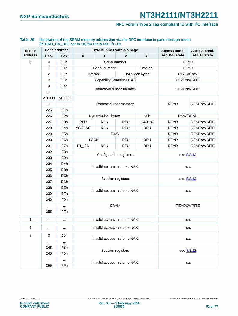
NXP Semiconductors NT3H2111/NT3H2211NFC Forum Type 2 Tag compliant IC with I2C interface
Table 39. Illustration of the SRAM memory addressing via the NFC interface in pass-through mode (PTHRU_ON_OFF set to 1b) for the NTAG I2C 1k
Sectoraddress
Page address Byte number within a page Access cond.ACTIVE state
Access cond. AUTH. stateDec. Hex. 0 1 2 3
0 0 00h Serial number READ
1 01h Serial number Internal READ
2 02h Internal Static lock bytes READ/R&W
3 03h Capability Container (CC) READ&WRITE
4 04hUnprotected user memory READ&WRITE
... ...
AUTH0 AUTH0
Protected user memory READ READ&WRITE... ...
225 E1h
226 E2h Dynamic lock bytes 00h R&W/READ
227 E3h RFU RFU RFU AUTH0 READ READ&WRITE
228 E4h ACCESS RFU RFU RFU READ READ&WRITE
229 E5h PWD READ READ&WRITE
230 E6h PACK RFU RFU READ READ&WRITE
231 E7h PT_I2C RFU RFU RFU READ READ&WRITE
232 E8hConfiguration registers see 8.3.12
233 E9h
234 EAhInvalid access - returns NAK n.a.
235 EBh
236 EChSession registers see 8.3.12
237 EDh
238 EEhInvalid access - returns NAK n.a.
239 EFh
240 F0h
SRAM READ&WRITE... ...
255 FFh
1 ... ... Invalid access - returns NAK n.a.
2 ... ... Invalid access - returns NAK n.a.
3 0 00hInvalid access - returns NAK n.a.
... ...
248 F8hSession registers see 8.3.12
249 F9h
... ...Invalid access - returns NAK n.a.
255 FFh
NT3H2111/NT3H2211 All information provided in this document is subject to legal disclaimers. © NXP Semiconductors N.V. 2016. All rights reserved.
Product data sheetCOMPANY PUBLIC
Rev. 3.0 — 3 February 2016359930 62 of 77
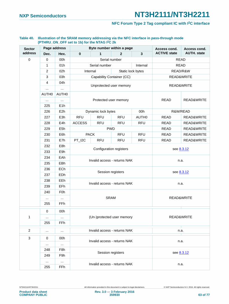
NXP Semiconductors NT3H2111/NT3H2211NFC Forum Type 2 Tag compliant IC with I2C interface
Table 40. Illustration of the SRAM memory addressing via the NFC interface in pass-through mode (PTHRU_ON_OFF set to 1b) for the NTAG I2C 2k
Sectoraddress
Page address Byte number within a page Access cond.ACTIVE state
Access cond. AUTH. stateDec. Hex. 0 1 2 3
0 0 00h Serial number READ
1 01h Serial number Internal READ
2 02h Internal Static lock bytes READ/R&W
3 03h Capability Container (CC) READ&WRITE
4 04hUnprotected user memory READ&WRITE
... ...
AUTH0 AUTH0
Protected user memory READ READ&WRITE... ...
225 E1h
226 E2h Dynamic lock bytes 00h R&W/READ
227 E3h RFU RFU RFU AUTH0 READ READ&WRITE
228 E4h ACCESS RFU RFU RFU READ READ&WRITE
229 E5h PWD READ READ&WRITE
230 E6h PACK RFU RFU READ READ&WRITE
231 E7h PT_I2C RFU RFU RFU READ READ&WRITE
232 E8hConfiguration registers see 8.3.12
233 E9h
234 EAhInvalid access - returns NAK n.a.
235 EBh
236 EChSession registers see 8.3.12
237 EDh
238 EEhInvalid access - returns NAK n.a.
239 EFh
240 F0h
SRAM READ&WRITE... ...
255 FFh
1
0 00h
(Un-)protected user memory READ&WRITE... ...
255 FFh
2 ... ... Invalid access - returns NAK n.a.
3 0 00hInvalid access - returns NAK n.a.
... ...
248 F8hSession registers see 8.3.12
249 F9h
... ...Invalid access - returns NAK n.a.
255 FFh
NT3H2111/NT3H2211 All information provided in this document is subject to legal disclaimers. © NXP Semiconductors N.V. 2016. All rights reserved.
Product data sheetCOMPANY PUBLIC
Rev. 3.0 — 3 February 2016359930 63 of 77
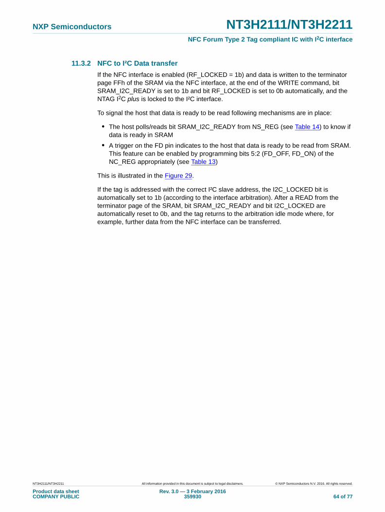
NXP Semiconductors NT3H2111/NT3H2211NFC Forum Type 2 Tag compliant IC with I2C interface
11.3.2 NFC to I²C Data transfer
If the NFC interface is enabled (RF_LOCKED = 1b) and data is written to the terminator page FFh of the SRAM via the NFC interface, at the end of the WRITE command, bit SRAM_I2C_READY is set to 1b and bit RF_LOCKED is set to 0b automatically, and the NTAG I2C plus is locked to the I²C interface.
To signal the host that data is ready to be read following mechanisms are in place:
• The host polls/reads bit SRAM_I2C_READY from NS_REG (see Table 14) to know if data is ready in SRAM
• A trigger on the FD pin indicates to the host that data is ready to be read from SRAM. This feature can be enabled by programming bits 5:2 (FD_OFF, FD_ON) of the NC_REG appropriately (see Table 13)
This is illustrated in the Figure 29.
If the tag is addressed with the correct I²C slave address, the I2C_LOCKED bit is automatically set to 1b (according to the interface arbitration). After a READ from the terminator page of the SRAM, bit SRAM_I2C_READY and bit I2C_LOCKED are automatically reset to 0b, and the tag returns to the arbitration idle mode where, for example, further data from the NFC interface can be transferred.
NT3H2111/NT3H2211 All information provided in this document is subject to legal disclaimers. © NXP Semiconductors N.V. 2016. All rights reserved.
Product data sheetCOMPANY PUBLIC
Rev. 3.0 — 3 February 2016359930 64 of 77
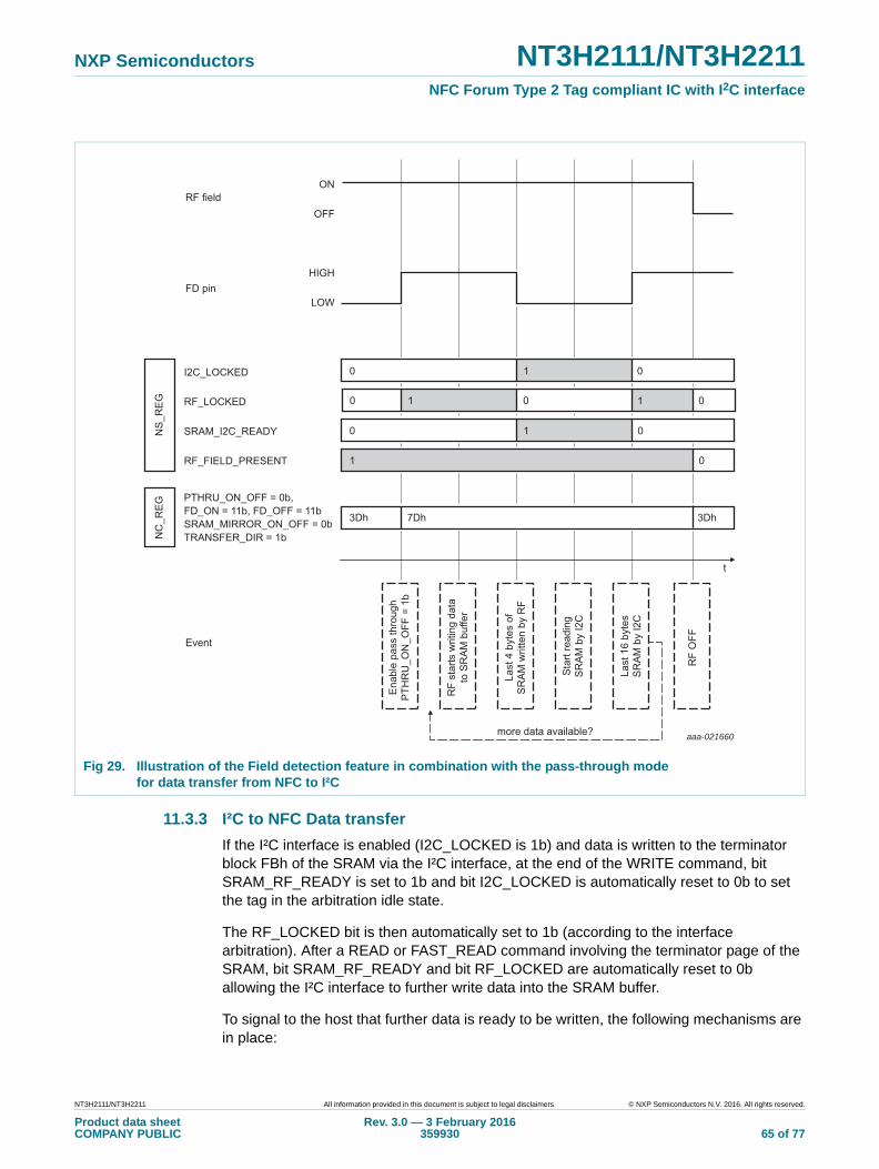
NXP Semiconductors NT3H2111/NT3H2211NFC Forum Type 2 Tag compliant IC with I2C interface
11.3.3 I²C to NFC Data transfer
If the I²C interface is enabled (I2C_LOCKED is 1b) and data is written to the terminator block FBh of the SRAM via the I²C interface, at the end of the WRITE command, bit SRAM_RF_READY is set to 1b and bit I2C_LOCKED is automatically reset to 0b to set the tag in the arbitration idle state.
The RF_LOCKED bit is then automatically set to 1b (according to the interface arbitration). After a READ or FAST_READ command involving the terminator page of the SRAM, bit SRAM_RF_READY and bit RF_LOCKED are automatically reset to 0b allowing the I²C interface to further write data into the SRAM buffer.
To signal to the host that further data is ready to be written, the following mechanisms are in place:
Fig 29. Illustration of the Field detection feature in combination with the pass-through mode for data transfer from NFC to I²C
aaa-021660
Ena
ble
pass
thro
ugh
PTH
RU
_ON
_OFF
= 1
b
RF
star
ts w
ritin
g da
tato
SR
AM
buf
fer
Last
4 b
ytes
of
SR
AM
writ
ten
by R
F
Sta
rt re
adin
gS
RA
M b
y I2
C
Last
16
byte
sS
RA
M b
y I2
C
ON
OFF
HIGH
LOW
RF field
FD pin
Event
I2C_LOCKED
RF_LOCKED
SRAM_I2C_READY
RF_FIELD_PRESENT
0
3Dh 7Dh
more data available?
3Dh
t
0
NS
_RE
G
PTHRU_ON_OFF = 0b,FD_ON = 11b, FD_OFF = 11bSRAM_MIRROR_ON_OFF = 0bTRANSFER_DIR = 1bN
C_R
EG
RF
OFF
1
0 01 0
0 1
0
0
1
1
NT3H2111/NT3H2211 All information provided in this document is subject to legal disclaimers. © NXP Semiconductors N.V. 2016. All rights reserved.
Product data sheetCOMPANY PUBLIC
Rev. 3.0 — 3 February 2016359930 65 of 77
NXP Semiconductors NT3H2111/NT3H2211NFC Forum Type 2 Tag compliant IC with I2C interface
• The NFC interface polls/reads the bit SRAM_RF_READY from NS_REG (see Table 14) to know if new data has been written by the I²C interface in the SRAM
• A trigger on the FD pin indicates to the host that data has been read from SRAM by the NFC interface. This feature can be enabled by programming bits 5:2 (FD_OFF, FD_ON) of the NC_REG appropriately (see Table 13)
The above mechanism is illustrated in the Figure 30.
Fig 30. Illustration of the Field detection signal feature in combination with pass-through mode for data transfer from I²C to NFC
1
aaa-021661
Ena
ble
pass
thro
ugh
PTH
RU
_ON
_OFF
= 1
b
I2C
sta
rts w
ritin
gda
ta to
SR
AM
buf
fer
Last
4 b
ytes
writ
ten
to S
RA
M b
y I2
C
Sta
rt re
adin
gS
RA
M b
y R
F
Last
4 b
ytes
read
by
RF
ON
OFF
HIGH
LOW
RF field
FD pin
Event
I2C_LOCKED
RF_LOCKED
SRAM_RF_READY
RF_FIELD_PRESENT
0
3Ch 7Ch
more data available?
3Ch
t
0 0
NS
_RE
G
PTHRU_ON_OFF = 0b,FD_ON = 11b, FD_OFF = 11bSRAM_MIRROR_ON_OFF = 0bTRANSFER_DIR = 0bN
C_R
EG
RF
OFF
1
0 01
0 1
0
0
1
NT3H2111/NT3H2211 All information provided in this document is subject to legal disclaimers. © NXP Semiconductors N.V. 2016. All rights reserved.
Product data sheetCOMPANY PUBLIC
Rev. 3.0 — 3 February 2016359930 66 of 77
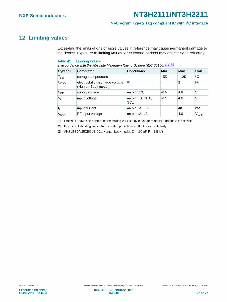
NXP Semiconductors NT3H2111/NT3H2211NFC Forum Type 2 Tag compliant IC with I2C interface
12. Limiting values
Exceeding the limits of one or more values in reference may cause permanent damage to the device. Exposure to limiting values for extended periods may affect device reliability.
[1] Stresses above one or more of the limiting values may cause permanent damage to the device.
[2] Exposure to limiting values for extended periods may affect device reliability.
[3] ANSI/ESDA/JEDEC JS-001; Human body model: C = 100 pF, R = 1.5 k.
Table 41. Limiting valuesIn accordance with the Absolute Maximum Rating System (IEC 60134).[1][2][3]
Symbol Parameter Conditions Min Max Unit
Tstg storage temperature 55 +125 C
VESD electrostatic discharge voltage (Human Body model)
[3] - 2 kV
VDD supply voltage on pin VCC -0.5 4.6 V
Vi input voltage on pin FD, SDA, SCL
-0.5 4.6 V
Ii input current on pin LA, LB - 40 mA
Vi(RF) RF input voltage on pin LA, LB - 4.6 Vpeak
NT3H2111/NT3H2211 All information provided in this document is subject to legal disclaimers. © NXP Semiconductors N.V. 2016. All rights reserved.
Product data sheetCOMPANY PUBLIC
Rev. 3.0 — 3 February 2016359930 67 of 77
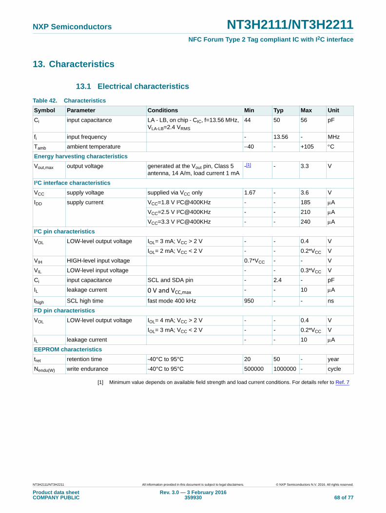
NXP Semiconductors NT3H2111/NT3H2211NFC Forum Type 2 Tag compliant IC with I2C interface
13. Characteristics
13.1 Electrical characteristics
[1] Minimum value depends on available field strength and load current conditions. For details refer to Ref. 7
Table 42. Characteristics
Symbol Parameter Conditions Min Typ Max Unit
Ci input capacitance LA - LB, on chip - CIC, f=13.56 MHz, VLA-LB=2.4 VRMS
44 50 56 pF
fi input frequency - 13.56 - MHz
Tamb ambient temperature 40 - +105 C
Energy harvesting characteristics
Vout,max output voltage generated at the Vout pin, Class 5 antenna, 14 A/m, load current 1 mA
-[1] - 3.3 V
I²C interface characteristics
VCC supply voltage supplied via VCC only 1.67 - 3.6 V
IDD supply current VCC=1.8 V I²C@400KHz - - 185 A
VCC=2.5 V I²C@400KHz - - 210 A
VCC=3.3 V I²C@400KHz - - 240 A
I²C pin characteristics
VOL LOW-level output voltage IOL= 3 mA; VCC > 2 V - - 0.4 V
IOL= 2 mA; VCC < 2 V - - 0.2*VCC V
VIH HIGH-level input voltage 0.7*VCC - - V
VIL LOW-level input voltage - - 0.3*VCC V
Ci input capacitance SCL and SDA pin - 2.4 - pF
IL leakage current 0 V and VCC,max - - 10 A
thigh SCL high time fast mode 400 kHz 950 - - ns
FD pin characteristics
VOL LOW-level output voltage IOL= 4 mA; VCC > 2 V - - 0.4 V
IOL= 3 mA; VCC < 2 V - - 0.2*VCC V
IL leakage current - - 10 A
EEPROM characteristics
tret retention time -40°C to 95°C 20 50 - year
Nendu(W) write endurance -40°C to 95°C 500000 1000000 - cycle
NT3H2111/NT3H2211 All information provided in this document is subject to legal disclaimers. © NXP Semiconductors N.V. 2016. All rights reserved.
Product data sheetCOMPANY PUBLIC
Rev. 3.0 — 3 February 2016359930 68 of 77
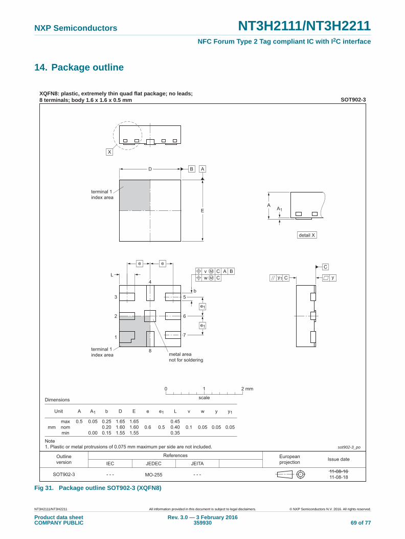
NXP Semiconductors NT3H2111/NT3H2211NFC Forum Type 2 Tag compliant IC with I2C interface
14. Package outline
Fig 31. Package outline SOT902-3 (XQFN8)
ReferencesOutlineversion
Europeanprojection Issue date
IEC JEDEC JEITA
SOT902-3 - - -MO-255- - -
sot902-3_po
11-08-1611-08-18
Unit
mmmaxnommin
0.5 0.05
0.00
1.651.601.55
1.651.601.55
0.6 0.5 0.1 0.05
A
Dimensions
Note1. Plastic or metal protrusions of 0.075 mm maximum per side are not included.
XQFN8: plastic, extremely thin quad flat package; no leads;8 terminals; body 1.6 x 1.6 x 0.5 mm SOT902-3
A1 b
0.250.200.15
D E e e1 L
0.450.400.35
v w
0.05
y y1
0.05
0 1 2 mm
scale
terminal 1index area
B AD
E
X
C
yCy1
terminal 1index area
3
L
e1
e
AC BvCw
2
1
5
6
7
metal areanot for soldering
8
4
e1
e
b
A1A
detail X
NT3H2111/NT3H2211 All information provided in this document is subject to legal disclaimers. © NXP Semiconductors N.V. 2016. All rights reserved.
Product data sheetCOMPANY PUBLIC
Rev. 3.0 — 3 February 2016359930 69 of 77
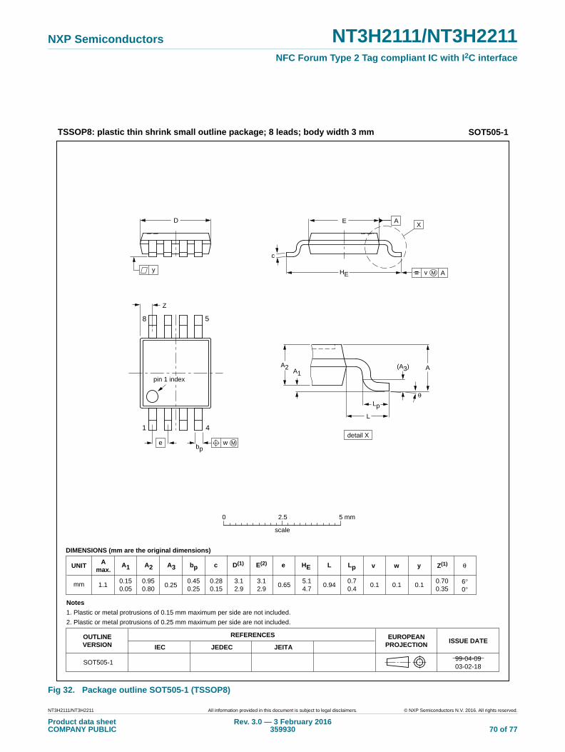
NXP Semiconductors NT3H2111/NT3H2211NFC Forum Type 2 Tag compliant IC with I2C interface
Fig 32. Package outline SOT505-1 (TSSOP8)
UNIT A1A
max.A2 A3 bp LHE Lp w yvc eD(1) E(2) Z(1) θ
REFERENCESOUTLINEVERSION
EUROPEANPROJECTION ISSUE DATE
IEC JEDEC JEITA
mm 0.150.05
0.950.80
0.450.25
0.280.15
3.12.9
3.12.9
0.655.14.7
0.700.35
6°0°
0.1 0.10.10.94
DIMENSIONS (mm are the original dimensions)
Notes
1. Plastic or metal protrusions of 0.15 mm maximum per side are not included.
2. Plastic or metal protrusions of 0.25 mm maximum per side are not included.
0.70.4
SOT505-1 99-04-0903-02-18
w Mbp
D
Z
e
0.25
1 4
8 5
θ
AA2A1
Lp
(A3)
detail X
L
HE
E
c
v M A
XA
y
2.5 5 mm0
scale
TSSOP8: plastic thin shrink small outline package; 8 leads; body width 3 mm SOT505-1
1.1
pin 1 index
NT3H2111/NT3H2211 All information provided in this document is subject to legal disclaimers. © NXP Semiconductors N.V. 2016. All rights reserved.
Product data sheetCOMPANY PUBLIC
Rev. 3.0 — 3 February 2016359930 70 of 77
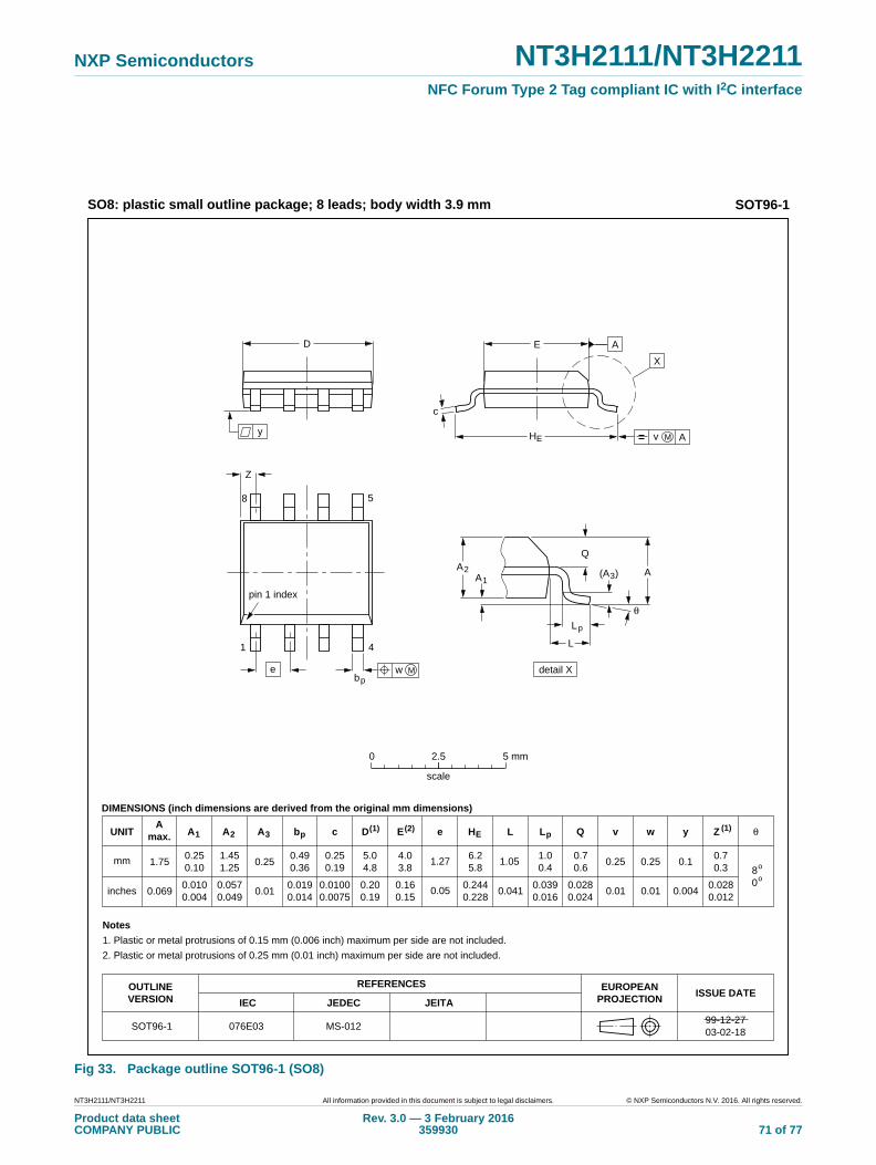
NXP Semiconductors NT3H2111/NT3H2211NFC Forum Type 2 Tag compliant IC with I2C interface
Fig 33. Package outline SOT96-1 (SO8)
UNITA
max. A1 A2 A3 bp c D(1) E(2) (1)e HE L Lp Q Zywv θ
REFERENCESOUTLINEVERSION
EUROPEANPROJECTION ISSUE DATE
IEC JEDEC JEITA
mm
inches
1.750.250.10
1.451.25
0.250.490.36
0.250.19
5.04.8
4.03.8
1.276.25.8
1.050.70.6
0.70.3 8
0
o
o
0.25 0.10.25
DIMENSIONS (inch dimensions are derived from the original mm dimensions)
Notes
1. Plastic or metal protrusions of 0.15 mm (0.006 inch) maximum per side are not included.
2. Plastic or metal protrusions of 0.25 mm (0.01 inch) maximum per side are not included.
1.00.4
SOT96-1
X
w M
θ
AA1
A2
bp
D
HE
Lp
Q
detail X
E
Z
e
c
L
v M A
(A )3
A
4
5
pin 1 index
1
8
y
076E03 MS-012
0.0690.0100.004
0.0570.049
0.010.0190.014
0.01000.0075
0.200.19
0.160.15
0.050.2440.228
0.0280.024
0.0280.012
0.010.010.041 0.0040.0390.016
0 2.5 5 mm
scale
SO8: plastic small outline package; 8 leads; body width 3.9 mm SOT96-1
99-12-2703-02-18
NT3H2111/NT3H2211 All information provided in this document is subject to legal disclaimers. © NXP Semiconductors N.V. 2016. All rights reserved.
Product data sheetCOMPANY PUBLIC
Rev. 3.0 — 3 February 2016359930 71 of 77
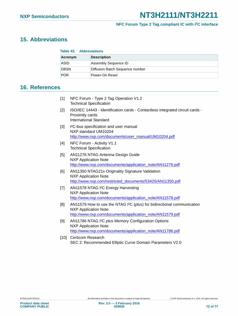
NXP Semiconductors NT3H2111/NT3H2211NFC Forum Type 2 Tag compliant IC with I2C interface
15. Abbreviations
16. References
[1] NFC Forum - Type 2 Tag Operation V1.2 Technical Specification
[2] ISO/IEC 14443 - Identification cards - Contactless integrated circuit cards - Proximity cardsInternational Standard
[3] I²C-bus specification and user manual NXP standard UM10204http://www.nxp.com/documents/user_manual/UM10204.pdf
[4] NFC Forum - Activity V1.1Technical Specification
[5] AN11276 NTAG Antenna Design GuideNXP Application Notehttp://www.nxp.com/documents/application_note/AN11276.pdf
[6] AN11350 NTAG21x Originality Signature ValidationNXP Application Notehttp://www.nxp.com/restricted_documents/53420/AN11350.pdf
[7] AN11578 NTAG I²C Energy HarvestingNXP Application Notehttp://www.nxp.com/documents/application_note/AN11578.pdf
[8] AN11579 How to use the NTAG I²C (plus) for bidirectional communicationNXP Application Notehttp://www.nxp.com/documents/application_note/AN11579.pdf
[9] AN11786 NTAG I²C plus Memory Configuration OptionsNXP Application Notehttp://www.nxp.com/documents/application_note/AN11786.pdf
[10] Certicom ResearchSEC 2: Recommended Elliptic Curve Domain Parameters V2.0
Table 43. Abbreviations
Acronym Description
ASID Assembly Sequence ID
DBSN Diffusion Batch Sequence number
POR Power-On Reset
NT3H2111/NT3H2211 All information provided in this document is subject to legal disclaimers. © NXP Semiconductors N.V. 2016. All rights reserved.
Product data sheetCOMPANY PUBLIC
Rev. 3.0 — 3 February 2016359930 72 of 77
NXP Semiconductors NT3H2111/NT3H2211NFC Forum Type 2 Tag compliant IC with I2C interface
17. Revision history
Table 44. Revision history
Document ID Release date Data sheet status Change notice Supersedes
NT3H2111_2211 v. 3.0 20160203 Product data sheet - -
NT3H2111/NT3H2211 All information provided in this document is subject to legal disclaimers. © NXP Semiconductors N.V. 2016. All rights reserved.
Product data sheetCOMPANY PUBLIC
Rev. 3.0 — 3 February 2016359930 73 of 77

NXP Semiconductors NT3H2111/NT3H2211NFC Forum Type 2 Tag compliant IC with I2C interface
18. Legal information
18.1 Data sheet status
[1] Please consult the most recently issued document before initiating or completing a design.
[2] The term ‘short data sheet’ is explained in section “Definitions”.
[3] The product status of device(s) described in this document may have changed since this document was published and may differ in case of multiple devices. The latest product status information is available on the Internet at URL http://www.nxp.com.
18.2 Definitions
Draft — The document is a draft version only. The content is still under internal review and subject to formal approval, which may result in modifications or additions. NXP Semiconductors does not give any representations or warranties as to the accuracy or completeness of information included herein and shall have no liability for the consequences of use of such information.
Short data sheet — A short data sheet is an extract from a full data sheet with the same product type number(s) and title. A short data sheet is intended for quick reference only and should not be relied upon to contain detailed and full information. For detailed and full information see the relevant full data sheet, which is available on request via the local NXP Semiconductors sales office. In case of any inconsistency or conflict with the short data sheet, the full data sheet shall prevail.
Product specification — The information and data provided in a Product data sheet shall define the specification of the product as agreed between NXP Semiconductors and its customer, unless NXP Semiconductors and customer have explicitly agreed otherwise in writing. In no event however, shall an agreement be valid in which the NXP Semiconductors product is deemed to offer functions and qualities beyond those described in the Product data sheet.
18.3 Disclaimers
Limited warranty and liability — Information in this document is believed to be accurate and reliable. However, NXP Semiconductors does not give any representations or warranties, expressed or implied, as to the accuracy or completeness of such information and shall have no liability for the consequences of use of such information. NXP Semiconductors takes no responsibility for the content in this document if provided by an information source outside of NXP Semiconductors.
In no event shall NXP Semiconductors be liable for any indirect, incidental, punitive, special or consequential damages (including - without limitation - lost profits, lost savings, business interruption, costs related to the removal or replacement of any products or rework charges) whether or not such damages are based on tort (including negligence), warranty, breach of contract or any other legal theory.
Notwithstanding any damages that customer might incur for any reason whatsoever, NXP Semiconductors’ aggregate and cumulative liability towards customer for the products described herein shall be limited in accordance with the Terms and conditions of commercial sale of NXP Semiconductors.
Right to make changes — NXP Semiconductors reserves the right to make changes to information published in this document, including without limitation specifications and product descriptions, at any time and without notice. This document supersedes and replaces all information supplied prior to the publication hereof.
Suitability for use — NXP Semiconductors products are not designed, authorized or warranted to be suitable for use in life support, life-critical or safety-critical systems or equipment, nor in applications where failure or malfunction of an NXP Semiconductors product can reasonably be expected to result in personal injury, death or severe property or environmental damage. NXP Semiconductors and its suppliers accept no liability for inclusion and/or use of NXP Semiconductors products in such equipment or applications and therefore such inclusion and/or use is at the customer’s own risk.
Applications — Applications that are described herein for any of these products are for illustrative purposes only. NXP Semiconductors makes no representation or warranty that such applications will be suitable for the specified use without further testing or modification.
Customers are responsible for the design and operation of their applications and products using NXP Semiconductors products, and NXP Semiconductors accepts no liability for any assistance with applications or customer product design. It is customer’s sole responsibility to determine whether the NXP Semiconductors product is suitable and fit for the customer’s applications and products planned, as well as for the planned application and use of customer’s third party customer(s). Customers should provide appropriate design and operating safeguards to minimize the risks associated with their applications and products.
NXP Semiconductors does not accept any liability related to any default, damage, costs or problem which is based on any weakness or default in the customer’s applications or products, or the application or use by customer’s third party customer(s). Customer is responsible for doing all necessary testing for the customer’s applications and products using NXP Semiconductors products in order to avoid a default of the applications and the products or of the application or use by customer’s third party customer(s). NXP does not accept any liability in this respect.
Limiting values — Stress above one or more limiting values (as defined in the Absolute Maximum Ratings System of IEC 60134) will cause permanent damage to the device. Limiting values are stress ratings only and (proper) operation of the device at these or any other conditions above those given in the Recommended operating conditions section (if present) or the Characteristics sections of this document is not warranted. Constant or repeated exposure to limiting values will permanently and irreversibly affect the quality and reliability of the device.
Terms and conditions of commercial sale — NXP Semiconductors products are sold subject to the general terms and conditions of commercial sale, as published at http://www.nxp.com/profile/terms, unless otherwise agreed in a valid written individual agreement. In case an individual agreement is concluded only the terms and conditions of the respective agreement shall apply. NXP Semiconductors hereby expressly objects to applying the customer’s general terms and conditions with regard to the purchase of NXP Semiconductors products by customer.
No offer to sell or license — Nothing in this document may be interpreted or construed as an offer to sell products that is open for acceptance or the grant, conveyance or implication of any license under any copyrights, patents or other industrial or intellectual property rights.
Document status[1][2] Product status[3] Definition
Objective [short] data sheet Development This document contains data from the objective specification for product development.
Preliminary [short] data sheet Qualification This document contains data from the preliminary specification.
Product [short] data sheet Production This document contains the product specification.
NT3H2111/NT3H2211 All information provided in this document is subject to legal disclaimers. © NXP Semiconductors N.V. 2016. All rights reserved.
Product data sheetCOMPANY PUBLIC
Rev. 3.0 — 3 February 2016359930 74 of 77
NXP Semiconductors NT3H2111/NT3H2211NFC Forum Type 2 Tag compliant IC with I2C interface
Export control — This document as well as the item(s) described herein may be subject to export control regulations. Export might require a prior authorization from competent authorities.
Quick reference data — The Quick reference data is an extract of the product data given in the Limiting values and Characteristics sections of this document, and as such is not complete, exhaustive or legally binding.
Non-automotive qualified products — Unless this data sheet expressly states that this specific NXP Semiconductors product is automotive qualified, the product is not suitable for automotive use. It is neither qualified nor tested in accordance with automotive testing or application requirements. NXP Semiconductors accepts no liability for inclusion and/or use of non-automotive qualified products in automotive equipment or applications.
In the event that customer uses the product for design-in and use in automotive applications to automotive specifications and standards, customer (a) shall use the product without NXP Semiconductors’ warranty of the product for such automotive applications, use and specifications, and (b) whenever customer uses the product for automotive applications beyond NXP Semiconductors’ specifications such use shall be solely at customer’s own risk, and (c) customer fully indemnifies NXP Semiconductors for any liability, damages or failed product claims resulting from customer design and use of the product for automotive applications beyond NXP Semiconductors’ standard warranty and NXP Semiconductors’ product specifications.
Translations — A non-English (translated) version of a document is for reference only. The English version shall prevail in case of any discrepancy between the translated and English versions.
18.4 Licenses
18.5 TrademarksNotice: All referenced brands, product names, service names and trademarks are the property of their respective owners.
MIFARE — is a trademark of NXP B.V.
I2C-bus — logo is a trademark of NXP B.V.
19. Contact information
For more information, please visit: http://www.nxp.com
For sales office addresses, please send an email to: [email protected]
Purchase of NXP ICs with NFC technology
Purchase of an NXP Semiconductors IC that complies with one of the Near Field Communication (NFC) standards ISO/IEC 18092 and ISO/IEC 21481 does not convey an implied license under any patent right infringed by implementation of any of those standards. Purchase of NXP Semiconductors IC does not include a license to any NXP patent (or other IP right) covering combinations of those products with other products, whether hardware or software.
NT3H2111/NT3H2211 All information provided in this document is subject to legal disclaimers. © NXP Semiconductors N.V. 2016. All rights reserved.
Product data sheetCOMPANY PUBLIC
Rev. 3.0 — 3 February 2016359930 75 of 77

NXP Semiconductors NT3H2111/NT3H2211NFC Forum Type 2 Tag compliant IC with I2C interface
20. Contents
1 General description . . . . . . . . . . . . . . . . . . . . . . 1
2 Features and benefits . . . . . . . . . . . . . . . . . . . . 22.1 Key features . . . . . . . . . . . . . . . . . . . . . . . . . . . 22.2 NFC interface . . . . . . . . . . . . . . . . . . . . . . . . . . 22.3 Memory. . . . . . . . . . . . . . . . . . . . . . . . . . . . . . . 32.4 I²C interface . . . . . . . . . . . . . . . . . . . . . . . . . . . 32.5 Security. . . . . . . . . . . . . . . . . . . . . . . . . . . . . . . 32.6 Key benefits . . . . . . . . . . . . . . . . . . . . . . . . . . . 3
3 Applications . . . . . . . . . . . . . . . . . . . . . . . . . . . . 4
4 Ordering information. . . . . . . . . . . . . . . . . . . . . 5
5 Marking . . . . . . . . . . . . . . . . . . . . . . . . . . . . . . . . 5
6 Block diagram . . . . . . . . . . . . . . . . . . . . . . . . . . 6
7 Pinning information. . . . . . . . . . . . . . . . . . . . . . 67.1 Pinning . . . . . . . . . . . . . . . . . . . . . . . . . . . . . . . 67.1.1 XQFN8 . . . . . . . . . . . . . . . . . . . . . . . . . . . . . . . 67.1.2 TSSOP8 . . . . . . . . . . . . . . . . . . . . . . . . . . . . . . 77.1.3 SO8 . . . . . . . . . . . . . . . . . . . . . . . . . . . . . . . . . 77.2 Pin description . . . . . . . . . . . . . . . . . . . . . . . . . 7
8 Functional description . . . . . . . . . . . . . . . . . . . 88.1 Block description . . . . . . . . . . . . . . . . . . . . . . . 88.2 NFC interface . . . . . . . . . . . . . . . . . . . . . . . . . . 88.2.1 Data integrity. . . . . . . . . . . . . . . . . . . . . . . . . . . 88.2.2 NFC state machine. . . . . . . . . . . . . . . . . . . . . . 98.2.2.1 IDLE state . . . . . . . . . . . . . . . . . . . . . . . . . . . . . 98.2.2.2 READY 1 state . . . . . . . . . . . . . . . . . . . . . . . . 108.2.2.3 READY 2 state . . . . . . . . . . . . . . . . . . . . . . . . 108.2.2.4 ACTIVE state . . . . . . . . . . . . . . . . . . . . . . . . . 108.2.2.5 AUTHENTICATED state . . . . . . . . . . . . . . . . . 108.2.2.6 HALT state . . . . . . . . . . . . . . . . . . . . . . . . . . . 108.3 Memory organization . . . . . . . . . . . . . . . . . . . 118.3.1 Memory map from NFC perspective. . . . . . . . 128.3.2 Memory map from I²C interface . . . . . . . . . . . 148.3.3 EEPROM . . . . . . . . . . . . . . . . . . . . . . . . . . . . 178.3.4 SRAM . . . . . . . . . . . . . . . . . . . . . . . . . . . . . . . 178.3.5 Serial number (UID) . . . . . . . . . . . . . . . . . . . . 178.3.6 Static Lock Bytes . . . . . . . . . . . . . . . . . . . . . . 188.3.7 Dynamic Lock Bytes . . . . . . . . . . . . . . . . . . . . 198.3.8 Capability Container (CC). . . . . . . . . . . . . . . . 218.3.9 User Memory pages . . . . . . . . . . . . . . . . . . . . 218.3.10 Memory content at delivery . . . . . . . . . . . . . . 228.3.11 Password and Access Configuration . . . . . . . 238.3.12 NTAG I2C configuration and session registers 258.4 Configurable Event Detection Pin. . . . . . . . . . 308.5 Watchdog timer. . . . . . . . . . . . . . . . . . . . . . . . 348.6 Energy harvesting. . . . . . . . . . . . . . . . . . . . . . 348.7 Password authentication . . . . . . . . . . . . . . . . 36
8.7.1 Programming of PWD and PACK. . . . . . . . . . 368.7.2 Limiting negative verification attempts . . . . . . 378.7.3 Protection of configuration segments. . . . . . . 378.8 Originality signature . . . . . . . . . . . . . . . . . . . . 37
9 I²C commands . . . . . . . . . . . . . . . . . . . . . . . . . 389.1 Start condition . . . . . . . . . . . . . . . . . . . . . . . . 389.2 Stop condition . . . . . . . . . . . . . . . . . . . . . . . . 389.3 I²C soft reset and NFC silence feature. . . . . . 399.4 Acknowledge bit (ACK) . . . . . . . . . . . . . . . . . 399.5 Data input. . . . . . . . . . . . . . . . . . . . . . . . . . . . 399.6 Addressing . . . . . . . . . . . . . . . . . . . . . . . . . . . 399.7 READ and WRITE Operation. . . . . . . . . . . . . 419.8 WRITE and READ register operation . . . . . . 43
10 NFC Command . . . . . . . . . . . . . . . . . . . . . . . . 4510.1 NTAG I2C plus command overview . . . . . . . . 4510.2 Timing . . . . . . . . . . . . . . . . . . . . . . . . . . . . . . 4510.3 NTAG ACK and NAK . . . . . . . . . . . . . . . . . . 4610.4 ATQA and SAK responses. . . . . . . . . . . . . . . 4610.5 GET_VERSION . . . . . . . . . . . . . . . . . . . . . . . 4710.6 READ_SIG. . . . . . . . . . . . . . . . . . . . . . . . . . . 4810.7 PWD_AUTH. . . . . . . . . . . . . . . . . . . . . . . . . . 5010.8 READ . . . . . . . . . . . . . . . . . . . . . . . . . . . . . . . 5110.9 FAST_READ . . . . . . . . . . . . . . . . . . . . . . . . . 5210.10 WRITE . . . . . . . . . . . . . . . . . . . . . . . . . . . . . . 5310.11 FAST_WRITE . . . . . . . . . . . . . . . . . . . . . . . . 5410.12 SECTOR SELECT . . . . . . . . . . . . . . . . . . . . . 55
11 Communication and arbitration between NFC and I²C interface . . . . . . . . . . . . . . . . . . . 57
11.1 Pass-through mode not activated . . . . . . . . . 5711.1.1 I²C interface access . . . . . . . . . . . . . . . . . . . . 5711.1.2 NFC interface access. . . . . . . . . . . . . . . . . . . 5711.2 SRAM buffer mapping with Memory Mirror
enabled . . . . . . . . . . . . . . . . . . . . . . . . . . . . . 5811.3 Pass-through mode . . . . . . . . . . . . . . . . . . . . 6111.3.1 SRAM buffer mapping . . . . . . . . . . . . . . . . . . 6111.3.2 NFC to I²C Data transfer . . . . . . . . . . . . . . . . 6411.3.3 I²C to NFC Data transfer . . . . . . . . . . . . . . . . 65
12 Limiting values . . . . . . . . . . . . . . . . . . . . . . . . 67
13 Characteristics . . . . . . . . . . . . . . . . . . . . . . . . 6813.1 Electrical characteristics . . . . . . . . . . . . . . . . 68
14 Package outline. . . . . . . . . . . . . . . . . . . . . . . . 69
15 Abbreviations . . . . . . . . . . . . . . . . . . . . . . . . . 72
16 References. . . . . . . . . . . . . . . . . . . . . . . . . . . . 72
17 Revision history . . . . . . . . . . . . . . . . . . . . . . . 73
18 Legal information . . . . . . . . . . . . . . . . . . . . . . 7418.1 Data sheet status . . . . . . . . . . . . . . . . . . . . . . 74
NT3H2111/NT3H2211 All information provided in this document is subject to legal disclaimers. © NXP Semiconductors N.V. 2016. All rights reserved.
Product data sheetCOMPANY PUBLIC
Rev. 3.0 — 3 February 2016359930 76 of 77
continued >>
NXP Semiconductors NT3H2111/NT3H2211NFC Forum Type 2 Tag compliant IC with I2C interface
18.2 Definitions. . . . . . . . . . . . . . . . . . . . . . . . . . . . 7418.3 Disclaimers . . . . . . . . . . . . . . . . . . . . . . . . . . . 7418.4 Licenses . . . . . . . . . . . . . . . . . . . . . . . . . . . . . 7518.5 Trademarks. . . . . . . . . . . . . . . . . . . . . . . . . . . 75
19 Contact information. . . . . . . . . . . . . . . . . . . . . 75
20 Contents . . . . . . . . . . . . . . . . . . . . . . . . . . . . . . 76
© NXP Semiconductors N.V. 2016. All rights reserved.
For more information, please visit: http://www.nxp.comFor sales office addresses, please send an email to: [email protected]
Date of release: 3 February 2016359930
Please be aware that important notices concerning this document and the product(s)described herein, have been included in section ‘Legal information’.