nvidia tegra 4 family gpu architecture · mobile devices are quickly becoming our most valuable...
TRANSCRIPT

Whitepaper
NVIDIA Tegra 4 Family
GPU Architecture
V1.0

P a g e | 2
NVIDIA Tegra 4 GPU Architecture February 2013
Table of Contents
...................................................................................................................................................................... 1
Introduction .................................................................................................................................................. 3
The Need for Fast Mobile GPUs .................................................................................................................... 3
Tegra 4 Family GPU Features and Architecture ............................................................................................ 4
Tegra 4 Family GPU Logical Pipeline Flow................................................................................................. 5
GPU Pipeline Implementation Details ...................................................................................................... 7
Vertex Processing Engines .................................................................................................................... 7
Raster Engine and Early-Z ..................................................................................................................... 8
VLIW Pixel Fragment Shader Pipelines ................................................................................................. 8
Texture Filtering Units .......................................................................................................................... 9
Additional GPU Features ..................................................................................................................... 10
Tegra 4 and Tegra 4i vs Tegra 3 Comparative Peformance Factors .................................................... 12
Tegra 4i GPU Architecture Diagram .................................................................................................... 13
Architectural Efficiency ............................................................................................................................... 14
Comparative Benchmark Performance ....................................................................................................... 16
Advanced Power Management................................................................................................................... 16
Tegra GPU / Memory Controller Interface ................................................................................................. 17
Enabling Advanced Graphics Effects in Mobile Games ............................................................................... 19
Developer Support .................................................................................................................................. 22
Conclusion ................................................................................................................................................... 23
Appendix A: Tegra 4 GPU Benchmarks ....................................................................................................... 24
Appendix B: Tegra 4 / 4i Supported Video and Audio Formats .................................................................. 24
Document Revision History ......................................................................................................................... 25

P a g e | 3
NVIDIA Tegra 4 GPU Architecture February 2013
Introduction
Mobile devices are quickly becoming our most valuable personal computers. Whether we’re
reading email, surfing the Web, interacting on social networks, taking pictures, playing games,
or using countless apps, our smartphones and tablets are becoming indispensable. Many
people are also using mobile devices such as Microsoft’s Surface RT and Lenovo’s Yoga 11
because of their versatile form-factors, ability to run business apps, physical keyboards, and
outstanding battery life.
Amazing new visual computing experiences are possible on mobile devices thanks to ever more
powerful GPU subsystems. A fast GPU allows rich and fluid 2D or 3D user interfaces, high
resolution display output, speedy Web page rendering, accelerated photo and video editing, and
more realistic 3D gaming. Powerful GPUs are also becoming essential for auto infotainment
applications, such as highly detailed and easy to read 3D navigation systems and digital
instrument clusters, or rear-seat entertainment and driver assistance systems.
Each new generation of NVIDIA® Tegra® mobile processors has delivered significantly higher
CPU and GPU performance while improving its architectural and power efficiency. Tegra
processors have enabled amazing new mobile computing experiences in smartphones and
tablets, such as full-featured Web browsing, console class gaming, fast UI and multitasking
responsiveness, and Blu-ray quality video playback.
At CES 2013, NVIDIA announced the Tegra 4 processor, the world’s first quad-core SoC using
four ARM Cortex-A15 CPUs, a Battery Saver Cortex A15 core, and a 72-core NVIDIA GPU.
With its increased number of GPU cores, faster clocks, and architectural efficiency
improvements, the Tegra 4 processor’s GPU delivers approximately 20x the GPU horsepower
of the Tegra 2 processor. The Tegra 4 processor also combines its CPUs, GPU, and ISP to
create a Computational Photography Engine for near-real-time HDR still frame photo and 1080p
30 video capture. Please see our whitepaper titled NVIDIA Tegra 4 Computational
Photography Architecture (Chimera) for more details.
Another version of the Tegra 4 processor called the Tegra 4i processor (codenamed Project
Grey) was announced in February 2013. The Tegra 4i processor is the highest performing
single-chip smartphone processor in its class and integrates an NVIDIA i500 LTE modem and
Quad Cortex-A9 r4 cores, plus a 60-core GPU. We’ll provide more details of the Tegra 4i GPU
in the Tegra 4 Family GPU Features and Architecture section.
The Need for Fast Mobile GPUs
One of the most popular application categories that demands fast GPU processing is 3D
games. Mobile 3D games have evolved from simple 2D visuals to now rival console gaming
experiences and graphics quality. In fact, some games that take full advantage of Tegra 4’s
GPU and CPU cores are hard to distinguish graphically from PC games! Not only have the
mobile games evolved, but mobile gaming as an application segment is one of the fastest
P a g e | 4
NVIDIA Tegra 4 GPU Architecture February 2013
growing in the industry today. Visually rich PC and console games such as Max Payne and
Grand Theft Auto III are now available on mobile devices.
High quality, high resolution retina displays (with resolutions high enough that the human eye
cannot discern individual pixels at normal viewing distances) are now being used in various
mobile devices. Such high resolution displays require fast GPUs to deliver smooth UI
interactions, fast Web page rendering, snappy high-res photo manipulation, and of course high
quality 3D gaming. Similarly, connecting a smartphone or tablet to an external high-resolution
4K screen absolutely requires a powerful GPU.
With two decades of GPU industry leadership, the mobile GPU in the NVIDIA® Tegra® 4 Family
of mobile processors is architected to deliver the performance demanded by console-class
mobile games, modern user interfaces, and high-resolution displays, while reducing power
consumption to fall within mobile power budgets. You will see that the Tegra 4 processor is also
the most architecturally efficient GPU subsystem in any mobile SoC today. Next, we’ll take a
detailed look at the high performance GPU implemented in the Tegra 4 processor.
Tegra 4 Family GPU Features and Architecture
The Tegra 4 processor’s GPU accelerates both 2D and 3D rendering. Although 2D rendering is
often considered a “given” nowadays, it’s critically important to the user experience. The 2D
engine of the Tegra 4 processor’s GPU provides all the relevant low-level 2D composition
functionality, including alpha-blending, line drawing, video scaling, BitBLT, color space
conversion, and screen rotations. Working in concert with the display subsystem and video
decoder units, the GPU also helps support 4K video output to high-end 4K video display.
The 3D engine is fully programmable, and includes high-performance geometry and pixel
processing capability enabling advanced 3D user interfaces and console-quality gaming
experiences. The GPU also accelerates Flash processing in Web pages and GPGPU (General
Purpose GPU) computing, as used in NVIDIA’s new Computational Photography Engine,
NVIDIA Chimera™ architecture, that implements near-real-time HDR photo and video
photography, HDR Panoramic image processing, and “Tap-to-Track” objecting tracking.
As shown in the Tegra 4 family diagram in Figure 1 below, the Tegra 4 processor includes a 72
core GPU subsystem. The Tegra 4’s processor’s GPU has 6x the number of shader processing
cores of the Tegra 3 processor, which translates to roughly 3-4x delivered game performance
and sometimes even higher. The NVIDIA Tegra 4i processor uses the same GPU architecture
as the Tegra 4 processor, but a 60 core variant instead of 72 cores. Even at 60 cores it delivers
an astounding amount of graphics performance for mainstream smartphone devices.

P a g e | 5
NVIDIA Tegra 4 GPU Architecture February 2013
Figure 1 NVIDIA Tegra 4 Family Architecture
Tegra 4 Family GPU Logical Pipeline Flow
The NVIDIA® Tegra 4® and Tegra 4i processors’ GPUs implement an immediate-mode pipeline
design tuned for high-performance and excellent power efficiency. Throughout the next few
sections, we’ll refer to the Tegra 4 processor, but the same logical pipeline details apply to the
Tegra 4i processor. Reducing off-chip memory accesses is critical to power efficiency and high
performance in mobile SoC processors. The Tegra 4 processor’s GPU includes on-chip vertex,
texture, and pixels caches to reduce off-chip memory accesses, and provide high hit rates when
servicing data requests. Early Z-culling logic helps ensure non-visible pixel fragments are
discarded before the pixel shading stage to avoid unnecessary shading work.
In Figure 2 you can see the block called “OpenGL API calls” that feeds the Primitive Processing
block. Application-level API calls are interpreted by the graphics driver and the driver sends
various commands and pointers to vertex and texture data to the GPU. Vertex buffers are
fetched and cached in a VBO Cache for subsequent reuse. Vertex shader programs execute in
the Vertex Shader units (also called Vertex Shader Pipeline or Vertex Processing Engine
(VPE)), performing operations such as transforms and deformations on character and object
geometry. The Primitives Assembly stage combines vertices to assemble primitives such as
lines and triangles, and any primitives that reside outside of the camera’s viewing area
(frustum), or are back-facing, are culled (removed) from the pipeline, and those that are
contained both inside and outside the viewing frustum have their outside portions clipped,

P a g e | 6
NVIDIA Tegra 4 GPU Architecture February 2013
because they should not be rendered. Edge and plane equations are calculated on the
primitives in preparation for rasterizing.
Figure 2 – Tegra 4 Logical Graphics Processing Pipeline
The Rasterizer converts primitives to pixels fragments to feed the pixel shader pipelines, and
the Early-Z unit can reject pixels that have depth (Z) values that would place them behind pixels
already in the framebuffer. Pixel Shader pipes then operate on pixel fragments that pass the Z-
test by running pixel shader programs on each pixel fragment. A programmable blend stage is
incorporated in the Pixel Shader allowing any type of blend mode to be implemented, not only
those found in the OpenGL spec.
The Pixel Cache (also called the Fragment Data Cache) caches writes to the framebuffer and is
useful in reducing off-chip framebuffer traffic for user interface pixels or other areas that have
high reuse, in addition to Early-Z testing.
The texture unit fetches and filters texture data to apply to a pixel, and frequently accessed
texture data is cached in both L1 texture caches present in each Texture Unit and in a shared
L2 texture cache that is shared by all four texture units. Finally, the processed pixels can be

P a g e | 7
NVIDIA Tegra 4 GPU Architecture February 2013
blended with existing framebuffer pixel information, or they can overwrite the current framebuffer
pixel data.
GPU Pipeline Implementation Details
We will discuss the NVIDIA® Tegra® 4 processor’s GPU physical pipeline below and refer to the
Tegra 4 processor, but many of the general descriptions, aside from unit counts, apply to the
Tegra 4i processor as well. The Tegra 4 processor’s GPU Architecture Diagram below (Figure
3) presents more details on the actual physical implementation of the Tegra 4 processor’s GPU
subsystem.
Starting from the top, rendering commands are fetched through Host/Front End units (not
shown). Next, indices and vertices are fetched directly from memory and cached by the IDX
unit. IDX then passes vertices to multiple Vertex Processing Engines (VPEs). The IDX unit also
supports DX9-level instancing, where a single draw command can make multiple instances of a
model, with each model using a different set of per-instance data.
Figure 3 – Tegra 4 GPU Architecture Diagram
Vertex Processing Engines
Vertices are processed by six VPE units in the Tegra 4 processor’s GPU, each including a
VEC4 ALU (arithmetic logic unit) that contains four MAD (Multiply-Add) units (where MAD units
are more commonly known as Vertex Cores). The Tegra 4 processor includes a total of 24
vertex cores which is 6x the number of vertex cores in the Tegra 3 processor. A 96-entry Vertex

P a g e | 8
NVIDIA Tegra 4 GPU Architecture February 2013
Buffer Object cache, split 16KB per VPE, allows vertex reuse and reduces off-chip memory
accesses. Architectural improvements have resulted in a performance increase of up to 1.5x
over the NVIDIA® Tegra® 3 processor per vertex pipe when running at the same clock. The
vertex shader cores use FP32 precision for their computation to ensure geometric accuracy.
As described in the Logical Pipeline section, primitives are assembled from the vertices, and
any primitives that aren’t visible or back-facing are culled, or if they extend beyond the view
frustum they are clipped. Edge and plane equations are calculated on the primitives in
preparation for rasterizing.
Raster Engine and Early-Z
The Raster Engine generates pixel fragments from the primitives and can provide eight pixel
fragments per clock to the Pixel Shader pipes, similar to the Tegra 3 processor. Both the Tegra
4 processor and the Tegra 4i processor now support 2x and 4x Multisample Antialiasing
(MSAA), 24-bit Z, and 8-bit Stencil processing. The Raster Unit generates pixel fragments
(samples when MSAA is enabled) with associated 24-bit Z and 8-bit stencil values.
The Early-Z unit works in concert with the Raster Unit and is an optimized version of the
implementation used in high end desktop GeForce GPUs. The Early-Z operation tests all the
pixels or samples for Z-depth, and only passes on pixels or samples that are visible. By
performing an Early-Z test and discarding hidden pixels, much wasted work fetching Z, color,
and texture data for hidden pixels is avoided, in addition to avoiding much unnecessary pixel
computation in the Pixel Shader pipes. Early-Z is able to detect and discard hidden pixels at a
rate of eight pixels/clock (8ppc).
Early-Z processing delivers improved performance and power savings by reducing memory
traffic between the GPU and off-chip memory. In rare situations, the programmer may require
certain pixels to be hidden until pixel processing is complete. For these cases, a late-stage
depth test occurs within the pixel shader and blend units.
VLIW Pixel Fragment Shader Pipelines
Each of the four Pixel Fragment Shader pipes in the Tegra 4 processor’s GPU includes three
ALUs, and each ALU contains four MAD units, for a total of 48 pixel shader cores (4 x 3 x 4). A
single MFU (Multi-Function Unit) is included per ALU for a total of 12 MFU units. The MFU units
process transcendental math (logs, exponents, trigonometric, functions), reciprocals, square
roots, and MOV operations.
The Fragment Shader pipelines implement a VLIW architecture, where a mix of different
instructions can be issued to the four MAD units and MFU unit in each ALU. Examples of
different VLIW instruction mixes are as follows:
4x MAD
2x DP2A + MFU
1x DP3A + 1xMAD + MFU
1x DP2A + 2xMAD + MFU

P a g e | 9
NVIDIA Tegra 4 GPU Architecture February 2013
1x DP4 + MFU
A total of 16KB of Pixel Cache is divided into four 4K L1 cache slices depicted in the
architecture diagram, and can reduce off-chip framebuffer access by over 50% in some cases.
Similar to prior NVIDIA® Tegra® processor GPUs, the Tegra 4 processor’s GPU uses FP20 pixel
shader precision for power efficiency. In our studies, differences in image quality between FP32
and FP20 pixel rendering are virtually unperceivable to the human eye, and the power savings
is substantial to warrant using FP20 in this generation SoC.
Separate vertex and pixel shader architecture, rather than unified architecture, is also used for
power efficiency reasons. The power savings derived from separate vertex and pixel shaders in
the Tegra 4 processor architecture outweigh the workload flexibility advantages of unified
shaders.
Texture Filtering Units
Each pixel shader unit also includes a Texture filtering unit capable of FP16 texture filtering,
which enables High Dynamic Range (HDR) rendering. The four texture units each have their
own L1 cache, and a 16K L2 texture cache (in both Tegra 4 and 4i processors) improves
performance by reducing texture fetches from external memory. Because of the typical locality
of texture memory accesses by the four texture units, the combination of L1 and L2 texture
caches reduces off-chip texture accesses by over 80% in most cases.
Similar to prior Tegra processor GPUs, the Tegra 4 processor implements very high quality 16x
anisotropic filtering. Anisotropic filtering is a technique employed to enhance the image quality
of textures on surfaces that are at oblique viewing angles. Each pixel on the screen typically
requires multiple texture elements to be fetched from texture maps in memory, filtered, and
applied to the pixel to change its color. When viewing a surface head-on, perpendicular to the
camera or viewer, an equal number of texture elements are usually sampled per pixel using a
square sample pattern. However, at extreme viewing angles when the image on the screen
extends further along one axis than another, taking equal number of samples in each axis from
the texture map would result in texture blurring along the axis that stretches out into the horizon.
In the image with the two runways in Figure 4, texture detail is blurred in the right runway for
sections that are closer to the horizon. The runway on the left has Anisotropic Filtering applied,
and you can see that the texture detail has improved significantly, as more texture samples are
taken along the axis that is stretched out. Similarly, you can see differences in sharpness
between 2x vs 16x Aniso in the test pattern. Adaptive filtering algorithms and efficient texture
cache management techniques deliver high texture quality without significantly increasing
memory transactions.

P a g e | 10
NVIDIA Tegra 4 GPU Architecture February 2013
Figure 4 - Improved texture quality from Anisotropic Filtering (images from http://en.wikipedia.org/wiki/Anisotropic_filtering )
Raster Operations
Raster Operations (ROP) are often performed in separate ROP units in our desktop GPUs, but
such operations (MSAA resolve, compression, blending, reading/writing the framebuffer, etc)
are performed within the pixel shader, blend unit, and texture units. Overall pixel output rate is
4ppc for the NVIDIA® Tegra® 4 processor (four color pixels per clock) which is double the Tegra
3 processor’s pixel output rate. But when factoring in the higher clock of the Tegra 4 / 4i
processors, their actual pixel fillrates are more than double the Tegra 3 processor’s pixel fillrate.
While 4ppc seems fairly meager versus mid-to-high-end desktop GPUs, 4 ppc output rates can
be found in value desktop GPUs that consume 30-60 watts, and now it’s being done in a mobile
SoC-based GPU that consumes just a few watts!
Additional GPU Features
The GPUs of the Tegra 4 and Tegra 4i processors include many other enhancements and
features that help deliver richer visuals, higher performance, and more immersive graphics
experiences in mobile devices including:

P a g e | 11
NVIDIA Tegra 4 GPU Architecture February 2013
2x/4x Multisample Antialiasing (MSAA)1
24-bit Z (versus 20-bit Z in the Tegra 3 processor) and 8-bit Stencil
4K x 4K texture size incl. Non-Power of Two textures (versus 2K x 2K in the Tegra 3
processor) – for higher quality textures, and easier to port full resolution textures from
console and PC games to the Tegra 4 processor. Good for high resolution displays.
16:1 Depth (Z) Compression and 4:1 Color Compression (versus none in the Tegra 3
processor) – this is lossless compression and is useful for reducing bandwidth to/from
the frame buffer, and especially effective in antialiasing processing when processing
multiple samples per pixel
Depth Textures
Percentage Closer Filtering for Shadow Texture Mapping and Soft Shadows
Texture border color eliminate coarse MIP-level bleeding
sRGB for Texture Filtering, Render Surfaces and MSAA down-filter
1 - CSAA is no longer supported in Tegra 4 processors
Tegra 4 / 4i processors do not explicitly support OpenGL ES 3.0 API due to not having a few
features such as FP32 pixel shaders or EAC/ETC2 texture compression format support, but
Tegra 4 / 4i processors do support many of the important ES 3.0 features as shown in Table 1 .
As stated earlier, we believe differences in image quality between FP32 and FP20 pixel
rendering are virtually unperceivable to the human eye, and the power savings is substantial to
warrant using FP20 in this generation SoC. Similarly, the Tegra 4 processor includes popular
texture compression formats such as DXT. We do not expect applications/games to use ES 3.0
for quite some time.

P a g e | 12
NVIDIA Tegra 4 GPU Architecture February 2013
Table 1 - Tegra 4 GPU OpenGL ES Features
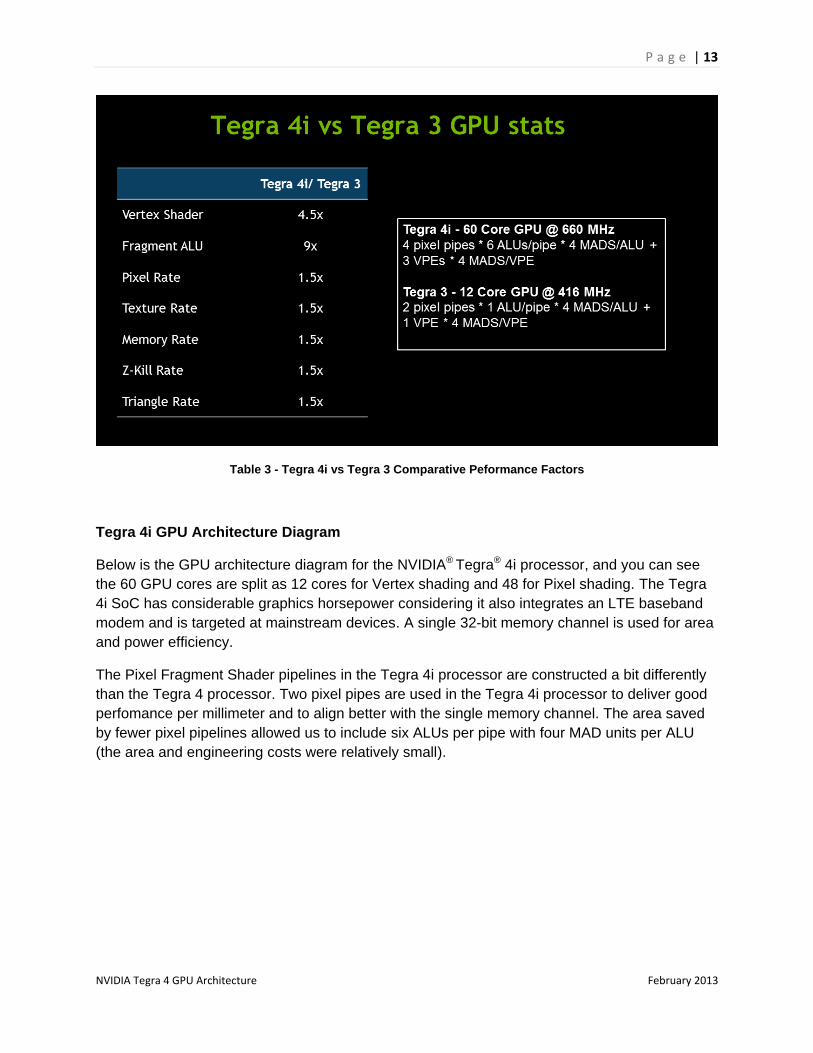
Tegra 4 and Tegra 4i vs Tegra 3 Comparative Peformance Factors
The tables below highlights the relative GPU unit performance differences of Tegra 4 and 4i
processors versus Tegra 3 processors. The values factor in not only architectural unit count
differences, but also architectural enhancements and clock rate increase of Tegra 4 and 4i
processors over Tegra 3 processors.
Table 2 - Tegra 4 vs Tegra 3 Comparative Peformance Factors
P a g e | 13
NVIDIA Tegra 4 GPU Architecture February 2013
Table 3 - Tegra 4i vs Tegra 3 Comparative Peformance Factors
Tegra 4i GPU Architecture Diagram
Below is the GPU architecture diagram for the NVIDIA® Tegra® 4i processor, and you can see
the 60 GPU cores are split as 12 cores for Vertex shading and 48 for Pixel shading. The Tegra
4i SoC has considerable graphics horsepower considering it also integrates an LTE baseband
modem and is targeted at mainstream devices. A single 32-bit memory channel is used for area
and power efficiency.
The Pixel Fragment Shader pipelines in the Tegra 4i processor are constructed a bit differently
than the Tegra 4 processor. Two pixel pipes are used in the Tegra 4i processor to deliver good
perfomance per millimeter and to align better with the single memory channel. The area saved
by fewer pixel pipelines allowed us to include six ALUs per pipe with four MAD units per ALU
(the area and engineering costs were relatively small).

P a g e | 14
NVIDIA Tegra 4 GPU Architecture February 2013
Figure 5 - Tegra 4i GPU Architecture Diagram
Architectural Efficiency
Two of the most important design criteria for microprocessors include optimizing performance
per watt and performance per square millimeter. The overarching term we like to use is
“architectural efficiency”. NVIDIA Tegra processor engineers tried to include as many advanced
features as possible in the NVIDIA Tegra 4 processor’s GPU, having strict perf/watt, perf/mm
targets, and die size and power constraints, while delivering industry-leading graphics quality,
features, and performance.
It can be readily seen in Table 4 that the Tegra 4 processor far surpasses the mobile
competition in the key architectural efficiency metrics of GFLOPs/mm2 , Fillrate/mm2, and in one
of the more popular mobile GPU benchmarks GLBench 2.5. The Tegra 4 processor is
considerably more efficient than any of the current competitive mobile GPUs. The GPU area
calculations normalized all SoCs to a 28nm process. (Note that the Tegra 4i processor was not
yet in a state to disclose detailed performance metrics at the time of this writing, so the next few
sections exclude the Tegra 4i processor.)

P a g e | 15
NVIDIA Tegra 4 GPU Architecture February 2013
Table 4 – Tegra 4 Architectural Efficiency Data versus Competitive GPUs
Similarly, Table 5 provides a graphical view of the above data so you can more readily see just
how much more efficient of a GPU architecture the NVIDIA® Tegra® 4 processor is versus
contemporary competitive mobile GPU designs.
Table 5 - Tegra 4 Architectural Efficiency Chart versus Competitive GPUs

P a g e | 16
NVIDIA Tegra 4 GPU Architecture February 2013
Comparative Benchmark Performance
The following benchmark chart depicts performance of the NVIDIA® Tegra® 4 processor’s GPU on two top synthetic GPU benchmarks – Basemark Taiji and GLBench 2.5. At the time of this writing, the Tegra 4 processor was still being optimized prior to market release, and all the Tegra 4 processor’s numbers were measured on a reference tablet and thus subject to change. Qualcomm Snapdragon S4 Pro data was measured on an HTC Droid DNA phone, and the Qualcomm Snapdragon 800 were estimated results based on Qualcomm marketing claims.
Table 6 – Comparative Benchmark Performance
Advanced Power Management
The GPU core in the Tegra 4 processor implements several advanced power management
techniques to reduce power consumption including:
Multiple Levels of Clock Gating: The GPU implements several levels of clock gating
that shut off clocks to various units during idle conditions. The GPU implements function-
level clock gating mechanisms that can clock-gate various different idle blocks within the
GPU core. For example, when the pipeline isn’t performing any vertex shading tasks, the
VPE units can be clock-gated and put in a low power state until the next vertex shading
commands are received. Similarly, when the Pixel Shader units are working on tasks
such as math calculations that do not require texture fetches, the texture units can be
clock-gated. Also, if the GPU is just refreshing the device display and not actively
P a g e | 17
NVIDIA Tegra 4 GPU Architecture February 2013
rendering, the memory controller can opportunistically put system memory into low
power state.
Display Request Grouping: The GPU groups multiple display requests, and issues
these requests in bursts to system memory. Then the GPU informs the memory
controller (via timers) about the timing of the next request burst. In the idle period
between GPU display request bursts, the memory controller looks for opportunities to
aggressively and dynamically put system memory in low power states.
Dynamic Voltage and Frequency Scaling (DVFS): During period of low GPU
utilization, GPU clocks and voltage can be dropped to lower levels to greatly reduce idle
power consumption. When an incoming task is detected, the frequency and voltage
levels are immediately increased to the appropriate operating values to ensure higher
performance. The DVFS software intelligently raises the voltage and frequency only up
to a level that is required to deliver the performance demanded by the application. The
DVFS algorithm has very fine control over the frequency levels, and can increase or
decrease frequency in steps as small as 1 MHz.
Tegra GPU / Memory Controller Interface
Being built on a 28nm manufacturing process, the NVIDIA® Tegra® 4 SoC now includes a dual-
channel (2 x 32-bit) memory subsystem for increased performance. The memory subsystem is
shared by various SoC processing cores including CPU, GPU, Video and Audio. Up to 4GB of
physical memory can be addressed. Supported memory types for both Tegra 4 and 4i
processors include DDR3L-1866 and LPDDR3-1866, and the Tegra 4i processor also supports
LPDDR3-2133.
The Tegra Memory Controller (MC) maximizes memory utilization while providing minimum
latency access for critical CPU and GPU requests. An arbiter is used to prioritize requests,
optimizing memory access efficiency and utilization, and minimizing system power consumption.
The MC provides access to main memory for all internal devices. It optimizes access to shared
memory resources, balancing latency and efficiency to provide the best system performance
based on programmable parameters.
The MC is built by NVIDIA and is highly tuned to the specific requirements of the Tegra
processor’s GPU, and includes several optimizations that enhance GPU performance and
reduce power consumption including:
Dynamic Clock Speed Control (DCSC): DCSC enables the memory controller to
quickly ramp up operating frequency in response to advanced indicators from the GPU
core for system memory accesses, and quickly ramp down operating frequency to a
power saving levels when the GPU has completed its memory accesses.
GPU centric Memory Arbitration: The MC implements advanced arbitration schemes
to efficiently grant multiple clients access to system memory. The MC core has advanced
knowledge of the type and urgency of memory access requests coming in from a GPU

P a g e | 18
NVIDIA Tegra 4 GPU Architecture February 2013
client and implements a very fine tuned arbitration scheme that delivers high bandwidth
for bandwidth-hungry render and geometry requests.
GPU Request Grouping: When requests are made to access regions of memory that
are not contained within currently open banks, the MC has to close the currently opened
banks, and then activate new banks that include the desired memory cells or regions.
This process not only impacts latency and bandwidth, but also requires higher power
consumption. The NVIDIA® Tegra® 4 processor’s GPU is aware of the current system
memory configuration, and optimizes access patterns. The GPU can group together
memory requests that access the same memory bank. The MC controller can also re-
order independent memory requests into groups based on their memory bank access
pattern. Such features deliver higher efficiency memory accesses, and reduce power
consumption by limiting frequent memory bank switching.
Tegra 4 / Tegra 4i Memory Controller Enhancements vs Tegra 3: The memory
controller in the Tegra 4 and 4i processors includes additional buffering in both the MC
and client interfaces. Higher burst bandwidth and higher latency tolerance permit more
aggressive power saving. Enhanced request coalescing improves memory efficiency.

P a g e | 19
NVIDIA Tegra 4 GPU Architecture February 2013
Enabling Advanced Graphics Effects in Mobile Games
The NVIDIA® Tegra® 4 processor’s GPU delivers up to 6x the raw shading power of the Tegra 3
processor, enabling game developers to employ advanced graphical effects, detailed models,
and immersive environments to deliver differentiated and visually richer mobile gaming
experiences.
Table 7 highlights a few of the many advanced graphics effects that can now be included in
mobile games due to the superior performance and capabilities of the Tegra 4 processor.
Tegra 4 Feature Graphics Effects in Games
Up to 6x Higher Geometry and
Vertex shading performance
More realistic character models
More complex skinned characters
More realistic crowd scenes
More realistic geometric particles such as rocks,
plants, mountain terrains
Better dynamic meshes for more realistic water
waves, vortex effects etc.
Support for depth and shadow
textures
More realistic shadows in games that take into
account lighting variances, multiple light sources,
cascaded shadow maps, etc.
Higher Pixel shading performance
with support for advanced math
functions
Create expansive and detailed terrains
Enhanced detail for low polygon models
High Dynamic Range (HDR) lighting in games
Cube mapping for better dynamic reflections,
global illumination, and more realistic lighting
effects
Subsurface scattering effects for more realistic
translucency in objects such as skin, jade, metal,
etc.
Table 7 - Tegra 4 GPU enhancements for Richer Game Visuals

P a g e | 20
NVIDIA Tegra 4 GPU Architecture February 2013
The following screen shots compare NVIDIA® Tegra® 4 processor-enhanced versus non-Tegra 4
processor-enhanced versions of three games – RU Golf THD from Nutgee, Zombie Driver THD
by Exor Studios, and Dead on Arrival 2 by N3V. You can see significant improvements in visual
quality in the Tegra 4 processor-enhanced versions.
Figure 6 - RU Golf THD by Nutgee

P a g e | 21
NVIDIA Tegra 4 GPU Architecture February 2013
Figure 7 - Dead on Arrival 2 by N3V
Figure 8 - Zombie Driver THD by Exor Studios

P a g e | 22
NVIDIA Tegra 4 GPU Architecture February 2013
These unique NVIDIA® Tegra® processor advanced visual effects enable game developers to
deliver a superior and visually differentiated gaming experience compared to games that are
available for non-Tegra processor devices. Developers of the above games leveraged not only
the Tegra 4 processor’s GPU capabilities, but also NVIDIA’s rich experience in graphics and
gaming to deliver engaging and segment-leading gaming experiences.
The GPU horsepower of the Tegra 4 processor along with the quad core CPU complex will
further empower game developers to deliver games that include PC and console class features
such as realistic physics effects, dynamic lighting, HDR textures, advanced shadow effects,
higher geometry details, subsurface scattering, and dynamic reflections.
One of the often overlooked reasons why so many games running on NVIDIA Tegra processor-
enabled devices look so much better than on competitive devices is not just the advanced
hardware features, but also the software development assistance and development tools
NVIDIA can provide to game developers. NVIDIA has years of experience helping game
developers implement amazing graphics effects using customized algorithms that are tuned to
the GPU architecture. NVIDIA continues to invest heavily in development and debugging tools
to help ensure developers can deliver the highest quality gaming content on Tegra processor
devices that is also highlighted and made easily accessible to end users by the NVIDIA
TegraZone™ Android application.
Developer Support
NVIDIA listened to the needs of today’s mobile developers, delivering tools that allow
developers to focus on creating compelling game titles and high-performance applications
instead of blindly navigating through platform-specific minutiae.
Nsight Tegra, Visual Studio Edition, is the premiere environment for native Android
development, integrated into Microsoft Visual Studio. Nsight Tegra seamlessly integrates
Android development and Microsoft Visual Studio 2010, taking the pain out of native Android
development, providing native Android project management, compilation, and debugging within
the familiar Visual Studio development environment.
Tegra Profiler for Android is a multi-core CPU sampling profiler that provides an interactive
view of captured profiling data, helping improve overall application performance.
And finally PerfHUD ES provides in-depth analysis of OpenGL ES applications on Tegra
processor-based devices, targeting optimizations where they are most needed. The debugging
capabilities provide insight into GPU performance and bottleneck information, helping find the
causes for performance and rendering anomalies.

P a g e | 23
NVIDIA Tegra 4 GPU Architecture February 2013
Figure 9 – Tegra Development Tools
Development tools need to get out of the way and allow developers to do their jobs. NVIDIA’s
Tegra Developer Tools makes this possible, allowing developers to quickly and easily bring
console-quality games to the NVIDIA® Tegra processor.
Conclusion
The need for higher quality GPU subsystems in mobile devices will continue to increase as
mobile usage models rely more and more on faster graphics processing speed. For the best
user experiences, smartphones and tablets must provide highly responsive graphical user
interfaces, fast Web browsing capability, visually rich 3D gaming, and be able to drive higher
resolution displays. It goes without saying that mobile 3D gaming systems such as NVIDIA
Project Shield portable or Ouya-type devices can always benefit for increased GPU speed to
process and display more realistic gaming environments and characters.
Automotive infotainment systems are now requiring much more graphics horsepower for visual
instrumentation clusters, 3D navigation functions, intelligent driver assist tools, and HD
entertainment systems. And new use cases such as NVIDIA® Chimera™ architecture (NVIDIA’s
Computational Photography Architecture), requires a powerful GPU.
The GPU subsystem within the NVIDIA Tegra 4 Family of processors is enabling all of the
aforementioned graphics capabilities in mobile devices, and far surpasses the competition, as
seen in many of the top mobile GPU benchmarks. The Tegra 4 processor is expected to lead
the mobile industry in visual computing capability in 2013.

P a g e | 24
NVIDIA Tegra 4 GPU Architecture February 2013
Appendix A: Tegra 4 GPU Benchmarks
Appendix B: Tegra 4 / 4i Supported Video and Audio Formats
Video
Decode H.264 HP/MP/BP 4k x 2k 62.5Mbps @ 24p,1440p 62.5Mbps @ 30p;1080p 62.5Mbps @ 60p; VC1 AP/MP/SP 1080p 40Mbps @ 60i/30p; MPEG4 SP 1080p 10Mbps @ 30 fps; WebM VP8 1080p 60Mbps @ 60p, 1440p 60Mbps @ 30p; MPEG-2 MP 1080p 80Mbps @ 60i/60p
Encode H.264 (BP/MP/HP)1080p 50Mbps @ 60p, 1440p 50Mbps @ 30p; MPEG4 SP D1 1Mbps 30p; VP8 1080p 20Mbps @ 60p, 1440p 50 Mbps @ 30 fps
Audio
Decode AAC, AAC-LC, AAC+, eAAC+, MP3, WAV/PCM, AMR-NB, AMR-WB, BSAC, MPEG-2 Audio, Ogg Vorbis, WMA 10, WMA Lossless, WMA Pro LBR 10, MPEG-2, AC3
Encode AAC LC, AMR-NB, AMR-WB

P a g e | 25
NVIDIA Tegra 4 GPU Architecture February 2013
Document Revision History
Initial release 1.0

P a g e | 26
Notice ALL INFORMATION PROVIDED IN THIS WHITE PAPER, INCLUDING COMMENTARY, OPINION, NVIDIA DESIGN SPECIFICATIONS, REFERENCE BOARDS, FILES, DRAWINGS, DIAGNOSTICS, LISTS, AND OTHER DOCUMENTS (TOGETHER AND SEPARATELY, “MATERIALS”) ARE BEING PROVIDED “AS IS.” NVIDIA MAKES NO WARRANTIES, EXPRESSED, IMPLIED, STATUTORY, OR OTHERWISE WITH RESPECT TO MATERIALS, AND EXPRESSLY DISCLAIMS ALL IMPLIED WARRANTIES OF NONINFRINGEMENT, MERCHANTABILITY, AND FITNESS FOR A PARTICULAR PURPOSE. Information furnished is believed to be accurate and reliable. However, NVIDIA Corporation assumes no responsibility for the consequences of use of such information or for any infringement of patents or other rights of third parties that may result from its use. No license is granted by implication or otherwise under any patent or patent rights of NVIDIA Corporation. Specifications mentioned in this publication are subject to change without notice. This publication supersedes and replaces all information previously supplied. NVIDIA Corporation products are not authorized for use as critical components in life support devices or systems without express written approval of NVIDIA Corporation. Trademarks NVIDIA, the NVIDIA logo, Chimera, Tegra, TegraZone are trademarks or registered trademarks of NVIDIA Corporation in the United States and other countries. Other company and product names may be trademarks of the respective companies with which they are associated. Copyright © 2013 NVIDIA Corporation. All rights reserved.