nx7 series controller user manual -...
TRANSCRIPT
Maximum Value for OEMsSM
NX7 Series Controller
User Manual

Important User InformationSolid state equipment has operational characteristics differing from those of electromechanical equipment. Because of this difference, and also because of the wide variety of uses for solid state equipment, all persons responsible for applying this equipment must satisfy themselves that each intended application of this equipment is acceptable.
In no event will OE Max Controls be responsible or liable for indirect or consequential damages resulting from the use or application of this equipment.
The examples and diagrams in this manual are included solely for illustrative purposes. Because of the many variables and requirements associated with any particular installation, OE Max Controls cannot assume responsibility or liability for actual use based on the examples and diagrams.
No patent liability is assumed by OE Max Controls with respect to use of information, circuits, equipment, or software described in this manual.
Reproduction of the contents of this manual, in whole or in part, without written permission of OE Max Controls is prohibited.
Throughout this manual we use notes to make you aware of safety considerations.
Identifies information about practices or circumstances which may lead to serious personal injury or death, property damage, or economic loss.
Identifies information that is critical for successful application and understanding of the product.
Identifies information about practices or circumstances that can lead to minor personal injury, property damage, economic loss, or product malfunction. However, depending on circumstances, failure to follow the directions accompanying this symbol may also lead to serious consequences.
IMPORTANT
WARNING
ATTENTION

Contents
1. Introduction............................................................... 9Features.......................................................................................................... 9
Installation Environment ............................................................................ 11
2. System Configuration ............................................. 13System Configuration ................................................................................. 13
Digital Expansion I/O Configurations ........................................................ 14
NX7 Product List.......................................................................................... 15
Hardware Features ...................................................................................... 16
3. Specifications.......................................................... 17General Specifications ................................................................................ 17
Power Supply Specifications...................................................................... 17
Performance Specifications........................................................................ 18
Input Specifications..................................................................................... 19
Output Specifications.................................................................................. 20
Communication Specifications .................................................................. 22
Installation and Wiring................................................................................ 23
Status LEDs.................................................................................................. 26
4. Addressing and Operation....................................... 29Addressing Space ....................................................................................... 29
Bit and Word Addressing ........................................................................... 30
Double Word Addressing ........................................................................... 31
l/O Addressing ............................................................................................. 33
Special Internal Addresses ......................................................................... 35
Special Register (SR) Area.......................................................................... 39
Timer/Counter Area..................................................................................... 43
Absolute Addressing................................................................................... 45
Processor Operation Mode......................................................................... 46
3
4
5. Programming Instructions....................................... 49Basic Sequence Instructions ...................................................................... 49
Timer, Counter and Shift Register Instructions ........................................ 50
Comparison Instructions ............................................................................ 51
Substitution, Increment and Decrement Instructions .............................. 51
Arithmetic Instructions ............................................................................... 52
Logical Instructions ..................................................................................... 53
Rotation Instructions................................................................................... 53
Word Conversion Instructions ................................................................... 54
Bit Conversion Instructions ........................................................................ 55
Move Instructions........................................................................................ 56
Program Control Instructions..................................................................... 57
System Control Instructions....................................................................... 58
6. Special Functions .................................................... 59High-Speed Counter Input Function .......................................................... 59
Input Pulse Catch Function......................................................................... 65
Pulse Output Function (for Transistor Output Model) ............................. 66
Appendix - Using WinGPC ............................................ 71Wiring and Switch Settings........................................................................ 71
Going Online with WinGPC ........................................................................ 73
Programming and Downloading ............................................................... 76
Program Monitoring ................................................................................... 77
PLC Diagnostics........................................................................................... 79
Using a Password........................................................................................ 81
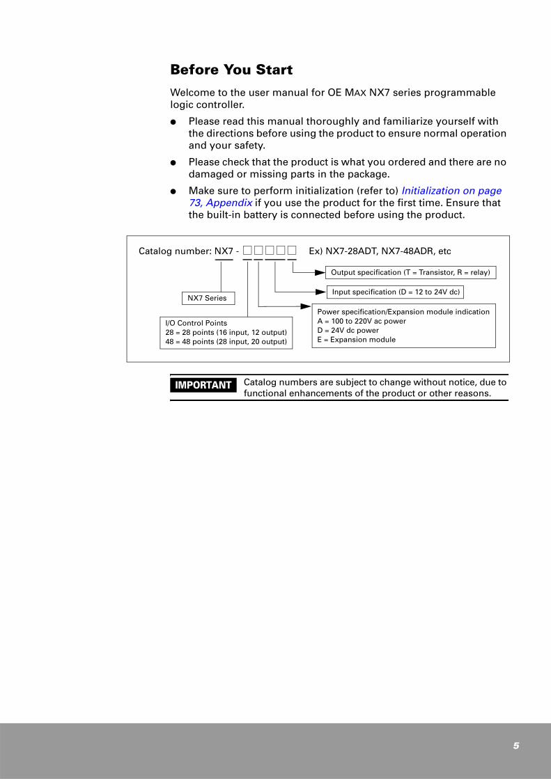
Before You Start
Welcome to the user manual for OE MAX NX7 series programmable logic controller.
Please read this manual thoroughly and familiarize yourself with the directions before using the product to ensure normal operation and your safety.
Please check that the product is what you ordered and there are no damaged or missing parts in the package.
Make sure to perform initialization (refer to) Initialization on page 73, Appendix if you use the product for the first time. Ensure that the built-in battery is connected before using the product.
Catalog number: NX7 - Ex) NX7-28ADT, NX7-48ADR, etc
Catalog numbers are subject to change without notice, due to functional enhancements of the product or other reasons.
Output specification (T = Transistor, R = relay)
Power specification/Expansion module indicationA = 100 to 220V ac powerD = 24V dc powerE = Expansion module
Input specification (D = 12 to 24V dc)NX7 Series
I/O Control Points28 = 28 points (16 input, 12 output)48 = 48 points (28 input, 20 output)
IMPORTANT
5

6
Safety Instructions
Please read this manual and the related documentation thoroughly and familiarize yourself with the directions before installing, operating, performing inspection and preventive maintenance. Make sure to follow the directions correctly to ensure normal operation of the product and your safety.
When designing a system using this product, consider proper prevention against external environmental fluctuations, power failure and noise, etc., in accordance with installation requirements. Design and implement an external circuit that allows your system to operate continually and safely in any system failure.
Make sure to disconnect the external power to the product before performing mounting, wiring, inspection, maintenance and cleaning. Never touch the power terminal when the power is on. Otherwise, it may cause an electrical shock.
Do not connect AC-powered products to a DC I/O terminal. Do not connect externally- powered products to an internal 24V DC output terminal.
If you need to perform a special operation during run, such as program editing, operation control or forced output, make sure to perform it after ensuring safety.
Do not connect an external device or a hand-held programmer (HHP) that uses internal power to the product when running. Make sure to stop the system and ensure safety before connecting them.
Make sure to use an external device to PLC when configuring the protective circuit breakers for emergencies.
When the self-diagnostics functionality detects an error, such as internal arithmetic error, watchdog time error, and/or connection failure, power continues to be provided to the controller’s power supply so that your system still works. Design and configure the circuits so that your system runs safely under those conditions.
The internal 24V DC power supplied to the circuits inside the PLC may have voltage fluctuations, depending on the volume of load. These voltage fluctuations may cause malfunction of the PLC or I/O devices connected. Therefore, use the internal power within the allowed rating.
Do not apply an impact to the terminal blocks or the product itself when the power is on. Otherwise, it may cause malfunction and failure of the product, or electrical shock.

Operate and keep the product under the allowed conditions directed in product specifications. During installation, be sure that all debris (metal chips, wire stands, etc.) is kept from falling into the product.
Do not expose the product to high temperature, high humidity, dusty conditions, salt, metal chips, corrosive gas, inflammable gas, solvents, abrasive oil, and/or direct sunlight.Avoid vibrations and crashes with other objects. Otherwise, it may cause a fire, damage, malfunction or aging to the product.
Fix cables as directed in the wiring instructions. We recommend you do not connect the line to the terminals marked with the symbol ''.
When wiring with the terminal block, use the following specifications: Screw: 3.0 M, Torque: 0.5 N . m (5 kgf .cm)Terminal width: 6.35 mm or less (0.25 in)
Input/output and communication cables should be separated from power cables. Give at least 200 mm space between them. Otherwise, generated noise may cause product malfunction.
We recommend installing an insulation transistor near the front of the PLC. Make sure to use twisted cables to prevent input noise.
For frame grounding, perform class 3 grounding at 100Ω or less ground resistance or independent class D grounding using a 2mm2. Do not perform common grounding to high voltage devices.
Do not disassemble or remodel the product. If you need to repair the product, contact the service center.
This manual does not include detailed explanation on all of the instructions and functions supported by the product. Please refer to other related manuals for more information.
Use the product only for the purposes stated on the product or in this user manual.
When disposing the product, make sure to follow your local regulations and guidelines on industrial waste disposal.
7

8

1
Introduction
Features
Small footprint and optimized functions
The NX7 PLC has a small footprint and is optimized to meet your environmental needs for control.
Designed optimally for micro to small scale applications that require up to 104 control points. Base 28 or 48 control points are provided by default. An expansion module provides 28 points and up to 2 expansion modules can be mounted. Therefore, max. 104 points (48 base points + 2 X 28 expansion points) are available.
Improves system productivity since major functions such as PID (proportional integral differential) control, high-speed counter, pulse output, and pulse catch are embedded in the processor module.
Provides one-to-many data exchange and two built-in communication ports, which enables your PLC system to connect directly to a touch screen and exchange large volume data at high speed.
Instructions modify while running
Designed to allow you to modify and execute Instructions quickly while the CPU is running.
High-capacity programming and memory backup
Up to 9k words program is supported. Flash ROM backup allows you to save your programs separately and safely.
Real time clock (RTC) and specialty function
The built-in real time clock function enables time and date related programming tasks. You can implement a simple link function that allows data communications between CPUs.
Compatibility of peripherals
Supports backward compatibility with the existing programming device (WinGPC), which allows easier programming, CPU state checkups, forced input/output, input/output monitoring, and program download and upload.
9

10
Two built-in communication ports
2 built-in communication ports allow easy connection to computers and peripheral devices without additional communication modules.
Self-diagnostics
The convenient self-diagnostics function makes your system diagnostics and troubleshooting easier.
Built-in PID control
Equipped with built-in 8-loop PID control logic, which allows you to easily implement applications for your analog control needs such as temperature and/or motion control.
Installation Environment
Do not install your PLC system under the following conditions:
• Ambient temperature outside the range of 0 to 55 °C(32 to 131 °F).
• Direct sunlight.
• Humidity outside the range of 20 to 90% (non-condensing).
• Chemicals that may affect electronic parts.
• Excessive or conductive dust, or salinity.
• High voltage, strong magnetic fields, or strong electromagnetic influences.
• Direct impact and excessive vibration.
• Organic solvents or cutting oil.
• Corrosive gas.
Follow these directions to prevent your PLC system from malfunctioning:
• Use an isolation transformer and noise filter on the incoming power to your controller system if there are any high capacity equipment, high voltage or strong electromagnetic influences nearby.
• Separate the main PLC grounding from all the groundings of other equipment. Make sure to use class 3 grounding.
• Make sure to use the external 24V dc power provided inside the NX7 module within the allowed ratings.
• Familiarize yourself with the PLC instructions and then design and implement your programs to ensure that system fault or malfunction is not caused by program error.
• Perform preventive maintenance to your PLC system, and inspect equipment and wiring status periodically. Make sure to ensure safety before operating your PLC system.
ATTENTION
ATTENTION
11

12

2
System Configuration
System Configuration
During running, do not connect any devices that are connected to the internal power supply and consume significant amount of instantaneous power. Make sure to connect them after stopping the system and ensuring safety.
COM1 (located at the front, 9-pin D-Sub type)
COM2 (located at the side, 8-pin modular type)
WinGPC version 3.5 or higher
28-point version 48-point version
ATTENTION
13
14
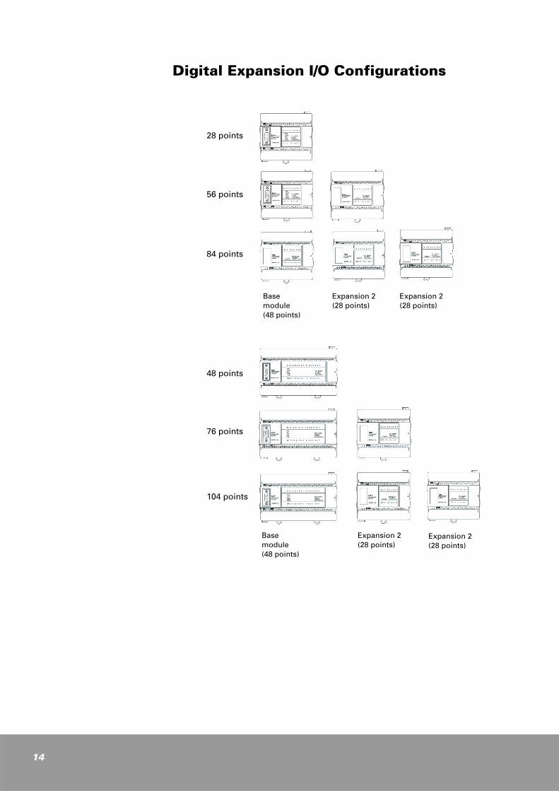
Digital Expansion I/O Configurations
28 points
56 points
84 points
48 points
76 points
104 points
Base module(48 points)
Expansion 2(28 points)
Expansion 2(28 points)
Base module(48 points)
Expansion 2(28 points)
Expansion 2(28 points)
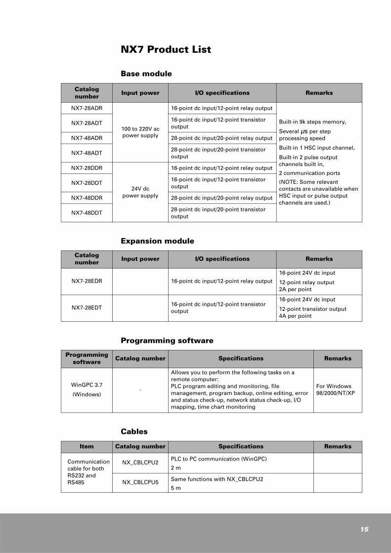
NX7 Product List
Base module
Expansion module
Programming software
Cables
Catalog number Input power I/O specifications Remarks
NX7-28ADR
100 to 220V acpower supply
16-point dc input/12-point relay output
Built-in 9k steps memory,
Several µs per step processing speed
Built-in 1 HSC input channel,
Built-in 2 pulse output channels built in,
2 communication ports
(NOTE: Some relevant contacts are unavailable when HSC input or pulse output channels are used.)
NX7-28ADT16-point dc input/12-point transistor output
NX7-48ADR 28-point dc input/20-point relay output
NX7-48ADT28-point dc input/20-point transistor output
NX7-28DDR
24V dc power supply
16-point dc input/12-point relay output
NX7-28DDT16-point dc input/12-point transistor output
NX7-48DDR 28-point dc input/20-point relay output
NX7-48DDT28-point dc input/20-point transistor output
Catalog number Input power I/O specifications Remarks
NX7-28EDR 16-point dc input/12-point relay output16-point 24V dc input
12-point relay output2A per point
NX7-28EDT16-point dc input/12-point transistor output
16-point 24V dc input
12-point transistor output4A per point
Programming software Catalog number Specifications Remarks
WinGPC 3.7
(Windows)-
Allows you to perform the following tasks on a remote computer: PLC program editing and monitoring, file management, program backup, online editing, error and status check-up, network status check-up, I/O mapping, time chart monitoring
For Windows 98/2000/NT/XP
Item Catalog number Specifications Remarks
Communication cable for both RS232 and RS485
NX_CBLCPU2PLC to PC communication (WinGPC)
2 m
NX_CBLCPU5 Same functions with NX_CBLCPU2
5 m
15
16
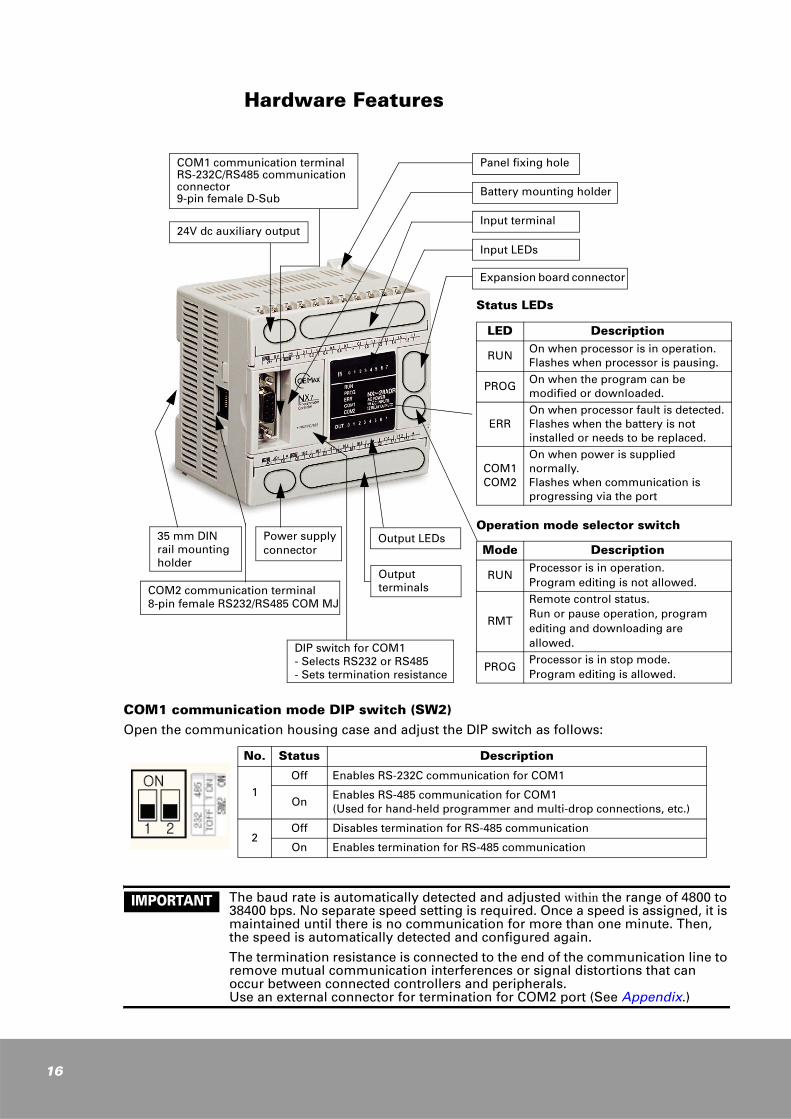
Hardware Features
COM1 communication mode DIP switch (SW2)Open the communication housing case and adjust the DIP switch as follows:
The baud rate is automatically detected and adjusted within the range of 4800 to 38400 bps. No separate speed setting is required. Once a speed is assigned, it is maintained until there is no communication for more than one minute. Then, the speed is automatically detected and configured again.
The termination resistance is connected to the end of the communication line to remove mutual communication interferences or signal distortions that can occur between connected controllers and peripherals.Use an external connector for termination for COM2 port (See Appendix.)
No. Status Description
1Off Enables RS-232C communication for COM1
OnEnables RS-485 communication for COM1(Used for hand-held programmer and multi-drop connections, etc.)
2Off Disables termination for RS-485 communication
On Enables termination for RS-485 communication
Power supplyconnector
Status LEDs
LED Description
RUNOn when processor is in operation.Flashes when processor is pausing.
PROGOn when the program can be modified or downloaded.
ERROn when processor fault is detected.Flashes when the battery is not installed or needs to be replaced.
COM1COM2
On when power is supplied normally.Flashes when communication is progressing via the port
Panel fixing holeCOM1 communication terminalRS-232C/RS485 communication connector9-pin female D-Sub
24V dc auxiliary output
35 mm DIN rail mountingholder
COM2 communication terminal8-pin female RS232/RS485 COM MJ
DIP switch for COM1- Selects RS232 or RS485- Sets termination resistance
Operation mode selector switch
Mode Description
RUNProcessor is in operation. Program editing is not allowed.
RMT
Remote control status. Run or pause operation, program editing and downloading are allowed.
PROGProcessor is in stop mode. Program editing is allowed.
Battery mounting holder
Input terminal
Input LEDs
Expansion board connector
Output LEDs
Output terminals
IMPORTANT

3
Specifications
General Specifications
Power Supply Specifications
Item Specifications
TemperatureOperating 0 to 55 °C
Storage -20 to 70 °C
Humidity Operating 10 to 90% RH (Non-condensing)
Withstand voltage1500V ac for 1 minute between external terminal (ac) and frame ground (FG)
500V ac for 1 minute between external terminal (dc) and frame ground (FG)
Allowed momentary power failure
20 ms or less
Noise immunity 1500 Vp-p pulse width 50 ns, 1 µ s (generated by noise simulator)
Insulation resistance 10 M Ω
Vibration immunity 10 to 55 Hz /1 min, amplitude 0.75 mm, each direction of X, Y, Z for 10 min
Dust condition No conductive dust
Chemicals No cutting oil and organic solvents
Corrosive gas No corrosive gas
Shock immunity 98m/S2 or more, 4 times X, Y, Z each direction
Grounding Class 3 grounding (100 Ω or less)
Case material PC/ABS
Cooling method Natural air cooling
Environ ment IP20
Item AC input power DC input power
Rated voltage 110 to 220V ac, free voltage 24V dc
Allowable voltage range 85 to 264V ac 24V ± 10% dc
Rated current consumption 33 Watts 33 Watts
Input power frequency 47 to 63 Hz -
Inrush current 3A or less 5A or less
Rated output currentFor internal power: 2.0A at 5VFor external output: 0.4A at 24V
For internal power: 2.0A at 5VFor external output: 0.4A at 24V
AC power circuit configuration 85 to 264V ac
FuseInternal circuit
17

18
Performance Specifications
Processor 28ADR/DDR/ADT/DDT, 48ADR/DDR/ADT/DDT
Control method Stored program, cyclic operation
External Input/outputBase 28/48 points. 28 expansion points. Expandable to max. two expansion modules
InstructionsBasic 28 types
Advanced 139 types
Processingspeed
Basic Several µs per step
Advanced Several to several tens of µs per step
Program capacity 9k words
Memory size
I/O (R) R000.00 to R31.15 (512 points, 32 words)
Special internal contact (R)
R032.00 to R127.15 (1436 points, 96 words)
Link contact (L) L000.00 to L063.15 (1024 points, 64 words)
Internal contact (M) M000.00 to M127.15 (2048 points, 128 words)
Keep contact (K) K000.00 to K127.15 (2048 points, 128 words)
Special contact (F) F000.00 to F015.15 (256 points, 16 words)
Timer/Counter(TC or TIM)
256 channels (Timer + Counter), Set value range: 0 to 65535
Timer: 0.01 Second: TC000 to TC063 (64 Channels)0.1 Second: TC064 to TC255 (192 Channels)
Counter: TC000 to TC255 (256 channels)
Data register (W) W0000 to W2047 (2048 words)
Special register (SR) SR000 to SR511 (512 words)
Communications
Speed 9600, 19200, 38400, 4800 bps, automatically selected
PortPort1: RS232/RS485, 9-pin female D-SUB
Port2: RS232/RS485, 8-pin modular terminal
Number of ports 2 ports
Supporting functions2 of 4 step communications protocol (Port 1 and 2)
User-defined communications, Modbus slave (Port 2)
Special functions
High-speed counter 1 channel/32 bits built-in, single phase 8K, two-phase 4K
Pulse output 2 channels built-in (TR output model) 5 KHz
Input pulse catch 4 contacts built-in
OthersRTC Built-in
PID Supports 8 loop PID control
ProgrammingTools
Programming S/W WinGPC
Memory backup Battery backup, Backup using flash ROM

Input Specifications
Internal circuit and wiring diagram- COM wiring (28-point model example)
+ COM wiring (48-point model example)
Use of 2-wire sensor may need an additional circuit configuration so that total current consumption does not exceed the allowable current consumption.
Item DC input
Input type DC voltage
Insulation method Photocoupler
Rated input voltage 12 to 24V dc
Voltage range 10.8 to 26.4V
Max. input current 10 mA or less
Min. On voltage/current 10.0V or more/3.0 mA or more
Max. Off voltage/current 5V or less/0.6 mA or less
Input impedance Approx. 3.6 K
Response time
Off → On 2 ms or less
On → Off 2 ms or less
Internal current consumption 50 mA or less at 5V
Polarity None
Common method 8 points per common or 16 points per common
Status display LED
External connection method Terminal block (M3.0), terminal width: 6.4 mm or less
Recommended wire size 0.5 to 1.25 mm2
Internal circuitSensor Sensor Two-wire sensor
Note
Sensor Sensor Two-wire sensor
Note
IMPORTANT
19

20
Output Specifications
Internal circuit and wiring diagram28 points (12 output points)
Item Relay output module
Catalog number 28xxR for relay output 48xxR for relay output
Output points 12 points 20 points
Insulation method Relay insulation
Rated input voltage 250V ac, 30V dc
Load voltage range 85 to 264V ac, 10 to 30V dc
Max. load current 2A per point. 6A per common (for 6 points)
Response time
Off → On 10 ms or less
On → Off 10 ms or less
Surge absorber Not applicable
Internal current consumption 300 mA or less at 5V 500 mA or less at 5V
Common method 1, 4, and 6 points per common
Status display LED
External connection method Terminal block (M3.0), terminal width: 6.4 mm or less
Recommended wire size 0.5 to 1.25 mm2
Internal circuit
48 points (20 output points)
Vcc OUT 2A
LOAD
COM 5 to 30V dc 100/200V ac

Internal circuit and wiring diagram
Item Transistor output
Catalog number 28xxT for transistor output 48xxT for transistor output
Output points 12 points 20 points
Insulation method Photocoupler
Rated load voltage 12 to 24V dc
Load voltage range 10 to 30V dc
Polarity - common (Sink type, NPN)
Max. load current 0.4A per point, 1.0A per common
Max. inrush current 3A, 10 ms or less
Off state leak current 100 uA or less
Response timeOff → On 1 ms or less
On → Off 1 ms or less
Internal current consumption (5V) 80 mA or less
Common method 1, 4, and 6 points per common
Status display LED
External connection method Terminal block (M3.0), terminal width: 6.4 mm or less
Recommended wire size 0.5 to 1.25 mm2
28 points (12 output points)
48 points (20 output points)
Internal circuit
24V dc Int’ Power
Vcc
OUT
COM
60 to 200mA
LOAD
10 to 30V dcInt’ OV
10 to 30V dc
10 to 30V dc
21

22
Communication Specifications
Use NX_CBLCPU2 or NX_CBLCPU5 cable from your personal computer's serial port to COM1 port. See Appendix, Using WinGPC Using WinGPC for more information about wiring.
Item Specifications Remarks
InterfaceCOM1: RS-232C or RS-485, 9-pin D-Sub DIP switch
COM2: RS-232C or RS-485, 8-pin modular Automatically recognized (wiring method)
Baud rate
38400, 19200, 9600, and 4800, automatically selected
(But, the speed is limited for COM2 user-defined communications)
Reset after pausing communication, for more than one minute, to change the speed.
Protocol Half duplex asynchronous polling
Data bit 8 bits
Parity None
Stop bit 1 bit
Communication distance
RS-232: 15 m or less, RS-485: 1.2 Km or less
Termination resistance
COM1: adjusted by the internal DIP switch
COM2: external user wiring (150 recommended)
Transmission cable
Twisted pair cable (Shielded cable)
1 NC
2 TXD
3 RXD
4 RTS
5 GND
6 485-
7 485+
8 CTS
9 Vcc
COM1 comm. port 9-pin female D-Sub
COM2 comm. port 8-pin female RJ45
Status LED(Flashes during communication)
COM1 switch settings
RS232/RS485 selector switch
Termination resistence setting switch
No Signal
1 485+
2 485-
3 485+
4 485-
5 Reserved
6 Signal GND
7 232C/RXD
8 232C/TXD
PLC Port1 (CoM1)(9-pin female D-sub)
PLC Port2 (CoM2)(8-pin female RJ45)
The terminals #1 and #3, and #2 and #4 are connected internally, respectively
IMPORTANT

Installation and Wiring
Avoid places where the temperature is outside of the range of 0 to 55 °C (32 to 131 °F), and the relative humidity is more than 85%.
Keep ambient temperature less than 55 °C (131 °F) by operating a fan or air conditioner if necessary.
Avoid places subject to rapid temperature fluctuations and condensation.
Avoid places exposed to direct sunlight.
Avoid the presence of water, corrosive or flammable gases, solvents, grinding fluids, cutting oil, dense dust, salinity, and/or debris (metal chips, wire stands, etc.).
Avoid places subject to direct impact or vibrations.
Allow sufficient space on all sides of the controller system for adequate ventilation.
Do not install the controller system near a control panel in which high-voltage devices are installed. Allow a minimum of 20 cm space from high-voltage line or power cable.
Environmental precautions for installation
Installation precautions
23

24
Product dimensions
* 28 points (base and expansion)
Installation dimensions
100 mm 79.0 mm
35 mm DIN rail mounting holder
76.6 mm
* 48 points
90 mm
146 mm
* 28 points * 48 points
unit: mm
100 mm
81.0 mm(31.9 in)
9.5
3.0
146.0 mm
126.0 mm(4.96 in)
87.0 mm(3.43 in)
10.0
3.0
1.5
10.0
Φ 4.2
87.0 mm(3.43 in)
90 mm
Installation space
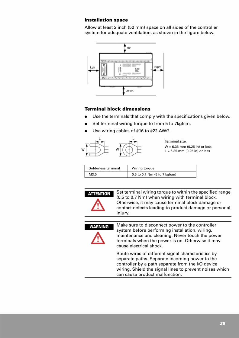
Allow at least 2 inch (50 mm) space on all sides of the controller system for adequate ventilation, as shown in the figure below.
Terminal block dimensions
Use the terminals that comply with the specifications given below.
Set terminal wiring torque to from 5 to 7kgfcm.
Use wiring cables of #16 to #22 AWG.
Set terminal wiring torque to within the specified range (0.5 to 0.7 Nm) when wiring with terminal block. Otherwise, it may cause terminal block damage or contact defects leading to product damage or personal injury.
Make sure to disconnect power to the controller system before performing installation, wiring, maintenance and cleaning. Never touch the power terminals when the power is on. Otherwise it may cause electrical shock.
Route wires of different signal characteristics by separate paths. Separate incoming power to the controller by a path separate from the I/O device wiring. Shield the signal lines to prevent noises which can cause product malfunction.
Solderless terminal Wiring torque
M3.0 0.5 to 0.7 Nm (5 to 7 kgfcm)
Terminal size
W = 6.35 mm (0.25 in) or lessL = 6.35 mm (0.25 in) or less
up
RightLeft
Down
W
L L
W
ATTENTION
WARNING
25

26
Power supply wiring
Make sure to connect to the controller system a stable power that has voltage fluctuations within 10% deviation from the rated input voltage. The frame ground terminal must be grounded with Class 3 (100Ω or less of ground resistance) or Class D grounding to prevent voltage mixing between the frame ground and the power input terminals.
Status LEDsThe following figure shows the LEDs indicating PLC status:
Processor LEDs
Five LEDs are used to indicate processor status:
is On when the processor is operating normally. Flashing indicates that the processor is pausing. Pause means that input/output is being progressed or the processor retains data.
is On when the program in the processor module can be edited.
is On when a processor error occurs or operation cannot proceed due to an abnormal program. Flashing indicates that a battery is not installed, or a minor error that does not hold processor operation has occurred.
flashes when communications are proceeding normally through COM1 port (9-pin D-Sub).
flashes when communications are proceeding normally through COM2 port (MJ).
Ground the frame ground terminal with a dedicated Class 3 (100 Ω or less of ground resistance) or Class D grounding.
* If the secondary side of the isolation transformer and the noise filter is too far from the controller system and noise becomes excessive, it does not have any significant effect.
Power sourceisolation
transformerNoise filter
Input LEDs
Processor LEDs
Output LEDs
RUN
PROG
ERR
COM1
COM2
Input LEDs
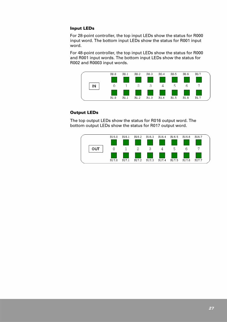
For 28-point controller, the top input LEDs show the status for R000 input word. The bottom input LEDs show the status for R001 input word.
For 48-point controller, the top input LEDs show the status for R000 and R001 input words. The bottom input LEDs show the status for R002 and R0003 input words.
Output LEDs
The top output LEDs show the status for R016 output word. The bottom output LEDs show the status for R017 output word.
27

28
4
Addressing and Operation
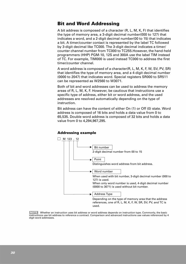
Addressing SpaceAll the memory used for external I/O processing and internal data processing has always both address and data (the content).
Addressing space is classified as R, L, M, K, F, W, TC, SV, PV, and SR. These letters are used to designate a specific area in memory as shown in the following table.
Memory areas Addresses Description
External I/O R000.00 to R31.15• I/O area • 512 points, 32 words
Special internal contact
R32.00 to R127.15• Special internal area• 1536 points, 96 words
Link contact L000.00 to L063.15
• Shared link area• 1024 points, 64 words• A point can be used as an internal contact when it is not
used for the link function.
Internal contact M000.00 to M127.15• Internal auxiliary area• 2048 points, 128 words
Keep contact K000.00 to K127.15• Retentive internal auxiliary area• 2048 points, 128 words• Clears when 'Reset retentive area' is performed.
Special contact F000.00 to F015.15• Special internal area• 256 points, 16 words
Timer/Counter
Channels: 0 to 255Set value: SV0 to SV255Current value: PV0 to PV255Contact: TC0 to TC255
• 256 shared channels (No duplicated use allowed)• TC indicates contact point area.• SV indicates set value area. PV indicates current or
present value area.• SV can be addressed to from 0 to 65535
Data register W0000 to W2047• Area that retains the data in case of power failure• Cannot be designated with a bit• Cleared when 'Initialize retentive area' is selected
Special register SR000 to SR511 • Special internal area for processor and RTC status
29
30
Bit and Word AddressingA bit address is composed of a character (R, L, M, K, F) that identifies the type of memory area, a 3-digit decimal number(000 to 127) that indicates a word, and a 2-digit decimal number(00 to 15) that indicates a bit. A timer/counter contact is represented by the label TC followed by 3-digit decimal like TC000. The 3-digit decimal indicates a timer/counter channel number from TC000 to TC255.However, the hand-held programmers (HHP) PGM-10, 12S and 300A use the label TIM instead of TC. For example, TIM000 is used instead TC000 to address the first timer/counter channel.
A word address is composed of a character(R, L, M, K, F, W, SV, PV, SR) that identifies the type of memory area, and a 4-digit decimal number (0000 to 2047) that indicates word. Special registers SR000 to SR511 can be represented as W2560 to W3071.
Both of bit and word addresses can be used to address the memory areas of R, L, M, K, F. However, be cautious that instructions use a specific type of address, either bit or word address, and the used addresses are resolved automatically depending on the type of instruction.
Bit address can have the content of either On (1) or Off (0) state. Word address is composed of 16 bits and holds a data value from 0 to 65,535. Double word address is composed of 32 bits and holds a data value from 0 to 4,294,967,295.
Addressing example
Whether an instruction uses bit address or word address depends on instruction type. Commonly, the basic instructions use bit address to reference a contract. Comparison and advanced instructions use values referenced by 4 digit word addresses.
Bit number
2-digit decimal number from 00 to 15
Point
Distinguishes word address from bit address.
Word number
When used with bit number, 3-digit decimal number (000 to 127) is used.When only word number is used, 4-digit decimal number (0000 to 3071) is used without bit number.
Address Type
Depending on the type of memory area that the address references, one of R, L, M, K, F, W, SR, SV, PV, and TC is used.
M 123 . 12
NOTE

Double Word Addressing Double word addressing is the same as word addressing, except
that 32-bit data is referenced by the specified address and its next address.
The type of instruction used determines which addressing, word or double word, is applied.
When using a double word comparison instruction with GPC5, press Ctrl+T in Edit mode to set the addressing mode to 'double', and then enter comparison instruction. The addresses you enter will be recognized as double word address. The character ‘D’ will appear in the instruction box on the ladder program to indicate double word addressing mode.
Example 1) ldentifying word and double word addressing
For example, as shown in the figure below, the double word, W0000, is composed of two words, W0000 and W0001. The bits of W0000 become the least significant bits (LSB) and those of W0001 become the most significant bits (MSB). Likewise, the double word address, W0001, represents the combination of two words W0001 and W0002. If a word is addressed in more than one place, like the word W0001 referenced by the two double words W0000 and W0001 as shown in the following figure, be cautious because duplicate use of the same
word may cause problems.
Word
Double word
With the parameter D or S, 1 word data (16 bits = 0 to 65535) are processed.
With the parameter D or S, 2 words data (32 bits = 0 to 4,294,967,295) are processed.
Addresses in double word addressing mode
31
32
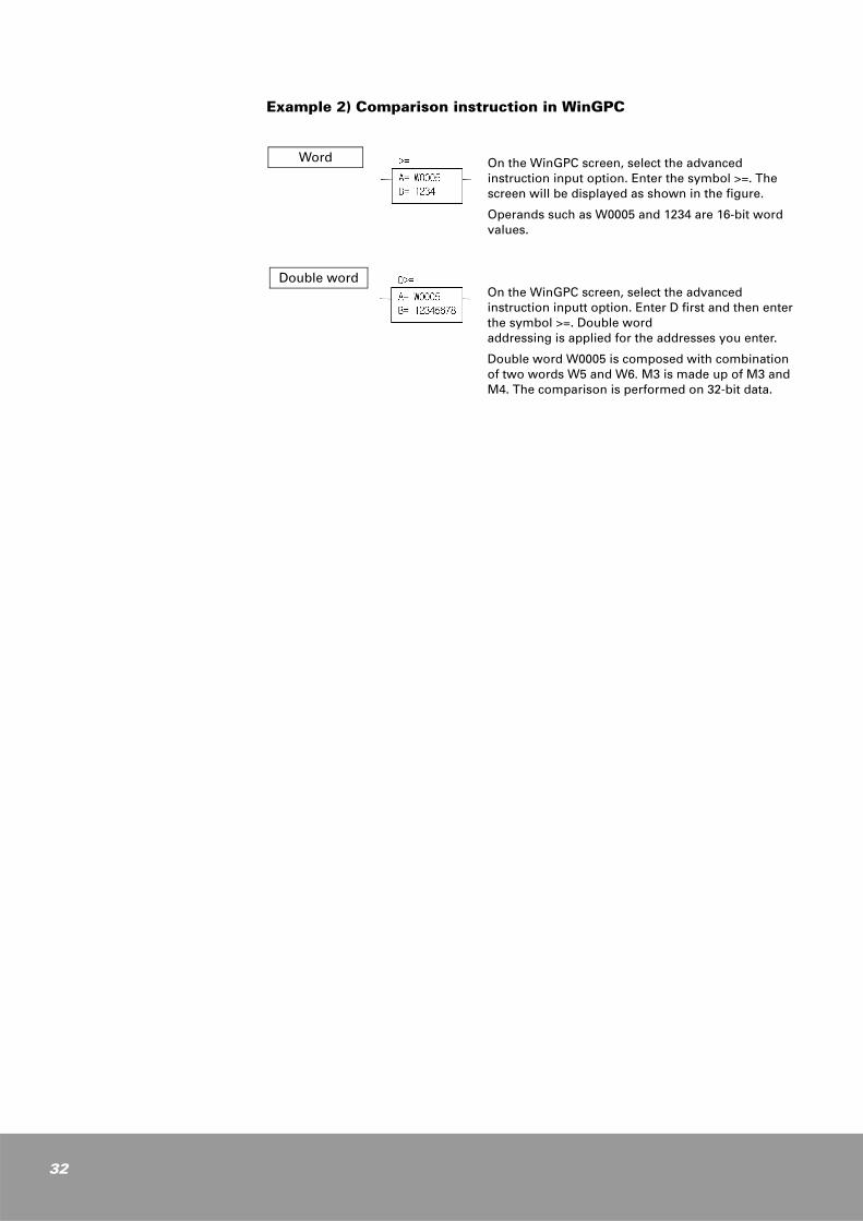
Example 2) Comparison instruction in WinGPC
Word
Double word
On the WinGPC screen, select the advanced instruction input option. Enter the symbol >=. The screen will be displayed as shown in the figure.
Operands such as W0005 and 1234 are 16-bit word values.
On the WinGPC screen, select the advanced instruction inputt option. Enter D first and then enter the symbol >=. Double word addressing is applied for the addresses you enter.
Double word W0005 is composed with combination of two words W5 and W6. M3 is made up of M3 and M4. The comparison is performed on 32-bit data.

l/O Addressing
Addressing is based on the location of the module.
I/O addressing method: Fixed addressing
I/O address range
- Input address: R000.00 to R015.07
- Output address: R016.00 to R031.07
- Special function address: R032 to R127 words (addressable as bit addresses.)
Addressing example
I/O addresses are allocated by byte. But, word addressing is used for internal arithmetic.The addresses of an expansion module are fixed. They are configured automatically as Expansion 1 or Expansion 2.
Base (8 words)Input: R00 to R07Output: R16 to R23
Expansion 1 (4 words)Input: R08 to R11Output: R24 to R27
Expansion 2 (4 words)Input: R12 to R15Output: R28 to R31
Input R0.0 to R1.7 Input R8.0 to R9.7 InputR12.0 to R13.7
Input R0.0 to R3.3 Input R8.0 to R9.7 Input R12.0 to R13.7
OutputR16.0 to R18.3 Output R24.0 to R25.3 Output R28.0 to R29.3
28 points 28 points 28 points
48 points 28 points 28 points
Output R24.0 to R25.3 Output R28.0 to R29.3Output R16.0 to R17.3
IMPORTANT
33

34
I/O LEDs
The following figures illustrate I/O LEDs and their corresponding memory addresses.
28-point base module Expansion 1 Expansion 2
48-point base module
Special Internal Addresses
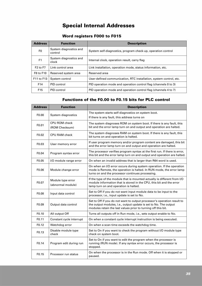
Word registers F000 to F015
Functions of the F0.00 to F0.15 bits for PLC control
Address Function Description
F0System diagnostics and control
System self-diagnostics, program check-up, operation control
F1System diagnostics and clock
Internal clock, operation result, carry flag
F2 to F7 Link control area Link installation, operation mode, status information, etc.
F8 to F10 Reserved system area Reserved area
F11 to F13 System control User-defined communication, RTC installation, system control, etc.
F14 PID control PID operation mode and operation control flag (channels 0 to 3)
F15 PID control PID operation mode and operation control flag (channels 4 to 7)
Address Function Description
F0.00 System diagnosticsThe system starts self-diagnostics on system boot.
If there is any fault, this address turns on
F0.01CPU ROM check
(ROM Checksum)The system diagnoses ROM on system boot. If there is any fault, this bit and the error lamp turn on and output and operation are halted.
F0.02 CPU RAM checkThe system diagnoses RAM on system boot. If there is any fault, this bit turns on and operation is halted.
F0.03 User memory errorIf user program memory and/or program content are damaged, this bit and the error lamp turn on and output and operation are halted.
F0.04 Program syntax errorThe processor verifies program syntax at the first run. If there is error, this bit and the error lamp turn on and output and operation are halted.
F0.05 I/O module range error On when an invalid address that is larger than R64 word is used.
F0.06 Module change errorOn when an I/O error occurs during system operation. If the operation mode is Remote, the operation is halted. In RUN mode, the error lamp turns on and the processor continues processing.
F0.07Module type error
(abnormal module)
If the type of the module that is mounted actually is different from I/O module information that is stored in the CPU, this bit and the error lamp turn on and operation is halted.
F0.08 Input data controlSet to Off if you do not want input module data to be input to the processor, i.e., input update is set to No.
F0.09 Output data controlSet to Off if you do not want to output processor's operation result to the output modules, i.e., output update is set to No. The output modules retain the last values prior to turning off this bit.
F0.10 All output Off Turns all outputs off in Run mode, i.e., sets output enable to No.
F0.11 Constant cycle interrupt On when a constant cycle interrupt instruction is being executed.
F0.12 Watchdog error On when a scan time exceeds the watchdog time.
F0.13Disable module type check
Set to On if you want to check the program without I/O module type check on system boot.
F0.14 Program edit during runSet to On if you want to edit the program when the processor is running (RUN mode). If any syntax error occurs, the processor is stopped.
F0.15 Processor run statusOn when the processor is in the Run mode. Off when it is stopped or paused.
35
36
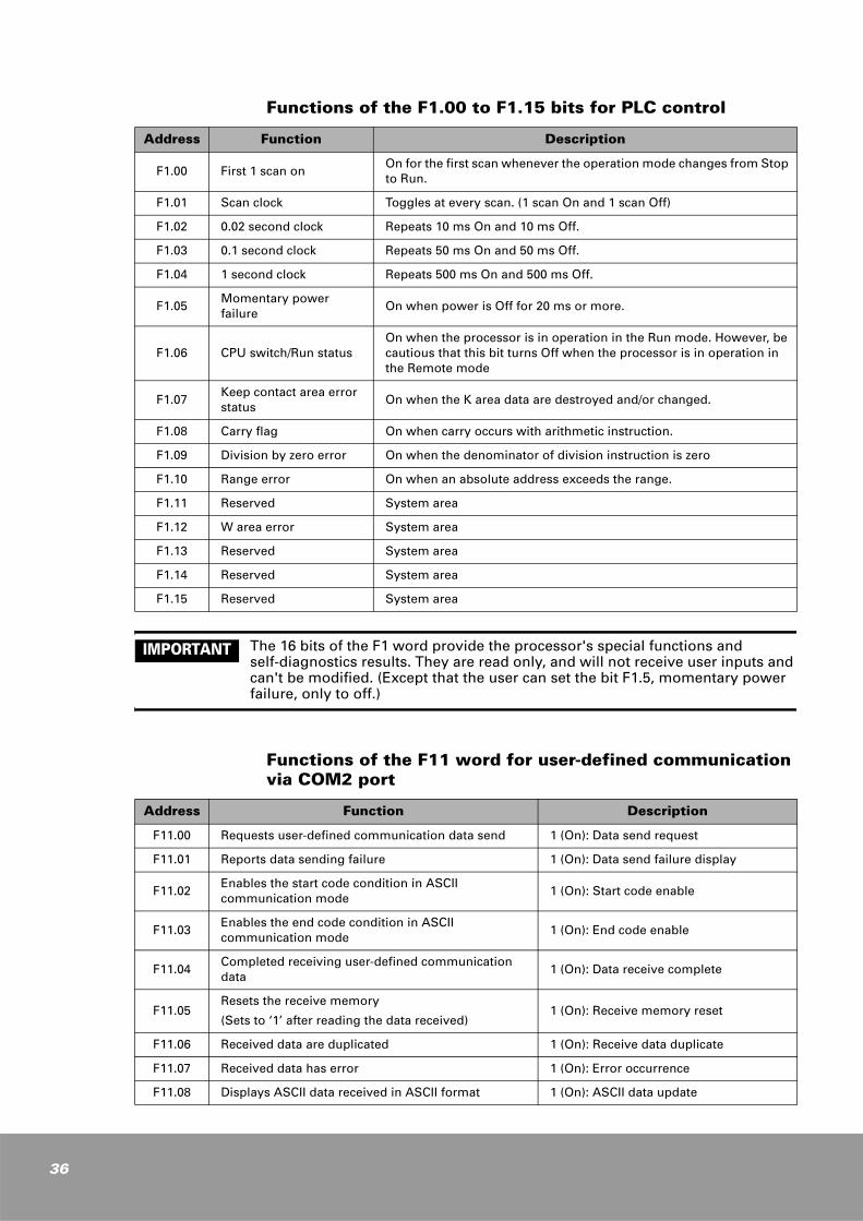
Functions of the F1.00 to F1.15 bits for PLC controlote
The 16 bits of the F1 word provide the processor's special functions and self-diagnostics results. They are read only, and will not receive user inputs and can't be modified. (Except that the user can set the bit F1.5, momentary power failure, only to off.)
Functions of the F11 word for user-defined communication via COM2 port
Address Function Description
F1.00 First 1 scan onOn for the first scan whenever the operation mode changes from Stop to Run.
F1.01 Scan clock Toggles at every scan. (1 scan On and 1 scan Off)
F1.02 0.02 second clock Repeats 10 ms On and 10 ms Off.
F1.03 0.1 second clock Repeats 50 ms On and 50 ms Off.
F1.04 1 second clock Repeats 500 ms On and 500 ms Off.
F1.05Momentary power failure
On when power is Off for 20 ms or more.
F1.06 CPU switch/Run statusOn when the processor is in operation in the Run mode. However, be cautious that this bit turns Off when the processor is in operation in the Remote mode
F1.07Keep contact area error status
On when the K area data are destroyed and/or changed.
F1.08 Carry flag On when carry occurs with arithmetic instruction.
F1.09 Division by zero error On when the denominator of division instruction is zero
F1.10 Range error On when an absolute address exceeds the range.
F1.11 Reserved System area
F1.12 W area error System area
F1.13 Reserved System area
F1.14 Reserved System area
F1.15 Reserved System area
Address Function Description
F11.00 Requests user-defined communication data send 1 (On): Data send request
F11.01 Reports data sending failure 1 (On): Data send failure display
F11.02Enables the start code condition in ASCII communication mode
1 (On): Start code enable
F11.03Enables the end code condition in ASCII communication mode
1 (On): End code enable
F11.04Completed receiving user-defined communication data
1 (On): Data receive complete
F11.05Resets the receive memory
(Sets to ‘1’ after reading the data received)1 (On): Receive memory reset
F11.06 Received data are duplicated 1 (On): Receive data duplicate
F11.07 Received data has error 1 (On): Error occurrence
F11.08 Displays ASCII data received in ASCII format 1 (On): ASCII data update
IMPORTANT
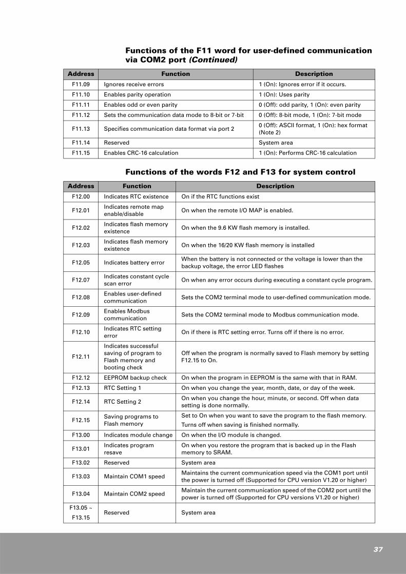
Functions of the F11 word for user-defined communication via COM2 port (Continued)
Functions of the words F12 and F13 for system control
Address Function Description
F11.09 Ignores receive errors 1 (On): Ignores error if it occurs.
F11.10 Enables parity operation 1 (On): Uses parity
F11.11 Enables odd or even parity 0 (Off): odd parity, 1 (On): even parity
F11.12 Sets the communication data mode to 8-bit or 7-bit 0 (Off): 8-bit mode, 1 (On): 7-bit mode
F11.13 Specifies communication data format via port 2 0 (Off): ASCII format, 1 (On): hex format (Note 2)
F11.14 Reserved System area
F11.15 Enables CRC-16 calculation 1 (On): Performs CRC-16 calculation
Address Function Description
F12.00 Indicates RTC existence On if the RTC functions exist
F12.01Indicates remote map enable/disable
On when the remote I/O MAP is enabled.
F12.02Indicates flash memory existence
On when the 9.6 KW flash memory is installed.
F12.03Indicates flash memory existence
On when the 16/20 KW flash memory is installed
F12.05 Indicates battery errorWhen the battery is not connected or the voltage is lower than the backup voltage, the error LED flashes
F12.07Indicates constant cycle scan error
On when any error occurs during executing a constant cycle program.
F12.08Enables user-defined communication
Sets the COM2 terminal mode to user-defined communication mode.
F12.09Enables Modbus communication
Sets the COM2 terminal mode to Modbus communication mode.
F12.10Indicates RTC setting error
On if there is RTC setting error. Turns off if there is no error.
F12.11
Indicates successful saving of program to Flash memory and booting check
Off when the program is normally saved to Flash memory by setting F12.15 to On.
F12.12 EEPROM backup check On when the program in EEPROM is the same with that in RAM.
F12.13 RTC Setting 1 On when you change the year, month, date, or day of the week.
F12.14 RTC Setting 2On when you change the hour, minute, or second. Off when data setting is done normally.
F12.15Saving programs to Flash memory
Set to On when you want to save the program to the flash memory.
Turns off when saving is finished normally.
F13.00 Indicates module change On when the I/O module is changed.
F13.01Indicates program resave
On when you restore the program that is backed up in the Flash memory to SRAM.
F13.02 Reserved System area
F13.03 Maintain COM1 speedMaintains the current communication speed via the COM1 port until the power is turned off (Supported for CPU version V1.20 or higher)
F13.04 Maintain COM2 speedMaintain the current communication speed of the COM2 port until the power is turned off (Supported for CPU versions V1.20 or higher)
F13.05 ~
F13.15Reserved System area
37

38
Functions of the F14 and F15 words for PID control
Address Function Description
F14.00
PID Loop0 control
Loop0 PID control - 1: operating, 0: stop
F14.01 Parameter range error flag - 1: error, 0: normal
F14.02 PID arithmetic mode - 1: manual, 0: auto
F14.03 PID control complete flag - 1: complete, 0: in operation
F14.04 to F14.07
PID Loop1 control Loop1 PID control: The functions are the same with Loop0.
F14.08 to F14.11
PID Loop2 control Loop2 PID control: The functions are the same with Loop0.
F14.12 to F14.15
PID Loop3 control Loop3 PID control: The functions are the same with Loop0.
F15.00 to F15.03
PID Loop4 control Loop4 PID control: The functions are the same with Loop0.
F15.04 to F15.07
PID Loop5 control Loop5 PID control: The functions are the same with Loop0.
F15.08 to F15.11
PID Loop6 control Loop6 PID control: The functions are the same with Loop0.
F15.12 to F15.15
PID Loop7 control Loop7 PID control: The functions are the same with Loop0.

Special Register (SR) AreaThe SR area consists of the range of SR000 (absolute address $0C00) to SR511 (absolute address $0DFF). Programmers who cannot use the SR key can use W2560 to W3071 instead.
The SR area and W area are essentially the same (ex: SR000 = W2560). In some cases, SR000 is automatically specified when W2560 is selected. 'SR' must be used in WinGPC.
Functions of SR000 (W2560) to SR511 (W3071)
Word addresses Function Description
SR000 to SR004 W2560 to W2564 CPU status Indicates current CPU status data.
SR005 to SR007 W2565 to W2567 Reserved System area
SR008 W2568 PID control Specifies the start address for PID control function
SR009 to SR016 W2569 to W2576 Reserved System area
SR017 to SR048 W2577 to W2608Program error information
Displays the detailed information about error that occurs during processing the program.
SR049 to SR288 W2609 to W2848 Reserved System area
SR289 to SR297 W2849 to W2857 RTC Sets and indicates real time clock information
SR298 to SR373 W2858 to W2933User-defined communication
Controls user-defined communication protocol for COM2 port.
SR374 to SR511 W2934 to W3071 Reserved System area
39
40
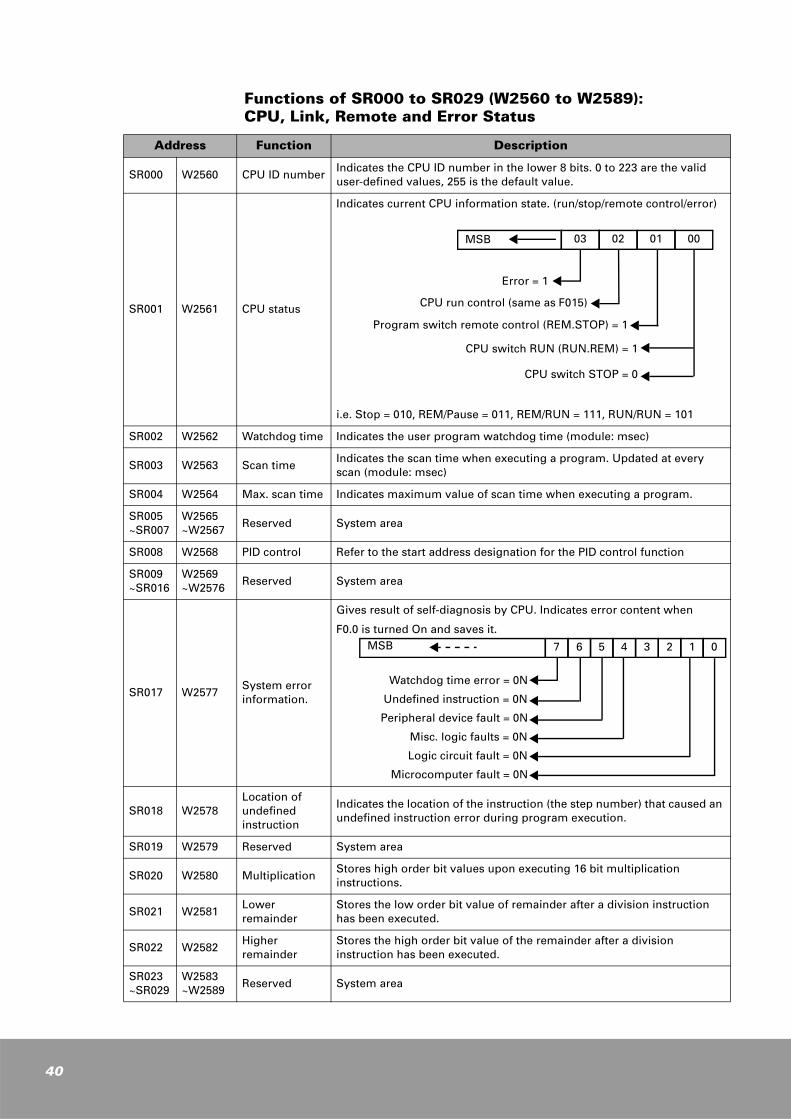
Functions of SR000 to SR029 (W2560 to W2589): CPU, Link, Remote and Error Status
Address Function Description
SR000 W2560 CPU ID numberIndicates the CPU ID number in the lower 8 bits. 0 to 223 are the valid user-defined values, 255 is the default value.
SR001 W2561 CPU status
Indicates current CPU information state. (run/stop/remote control/error)
i.e. Stop = 010, REM/Pause = 011, REM/RUN = 111, RUN/RUN = 101
SR002 W2562 Watchdog time Indicates the user program watchdog time (module: msec)
SR003 W2563 Scan timeIndicates the scan time when executing a program. Updated at every scan (module: msec)
SR004 W2564 Max. scan time Indicates maximum value of scan time when executing a program.
SR005 ~SR007
W2565 ~W2567
Reserved System area
SR008 W2568 PID control Refer to the start address designation for the PID control function
SR009 ~SR016
W2569 ~W2576
Reserved System area
SR017 W2577System error information.
Gives result of self-diagnosis by CPU. Indicates error content when
F0.0 is turned On and saves it.
SR018 W2578Location of undefined instruction
Indicates the location of the instruction (the step number) that caused an undefined instruction error during program execution.
SR019 W2579 Reserved System area
SR020 W2580 MultiplicationStores high order bit values upon executing 16 bit multiplication instructions.
SR021 W2581Lower remainder
Stores the low order bit value of remainder after a division instruction has been executed.
SR022 W2582Higher remainder
Stores the high order bit value of the remainder after a division instruction has been executed.
SR023 ~SR029
W2583 ~W2589
Reserved System area
MSB 03 02 01 00
Error = 1
CPU run control (same as F015)
Program switch remote control (REM.STOP) = 1
CPU switch RUN (RUN.REM) = 1
CPU switch STOP = 0
MSB 7 6 5 4
Watchdog time error = 0N
3 2 1 0
Undefined instruction = 0N
Peripheral device fault = 0N
Misc. logic faults = 0N
Logic circuit fault = 0N
Microcomputer fault = 0N

Functions of SR30 to SR48 (W2590 to W2608): Syntax Error Information
Address Function Detail
SR030 W2590Displays
error info.
Bit 0 = On if the I/O number range of bit instruction is beyond the specified range.
Bit 1 = On if the channel number of the timer or the counter exceeds 255 or is duplicated.
Bit 2 = On if the bit or word number in the advanced instruction is beyond the specified range or if it designates external address that cannot be used.
Bit 3 = On if a word number in the refresh instruction INPR or OUTR is beyond the specified range,
Bit 4 = On if an undefined instruction exists.
Bit 5 = On in event of a user program memory writing error.
Bit 6 = On in event of miscellaneous errors.
Bit 7 = On if the user program memory is abnormal.
Bit 8 = On if an error on external I/O address and bit/word/double word numbers used occurs.
Bit 9 = On if the label numbers of the JMP or CALL instructions exceed 63, the corresponding instruction LBL or SBR does not exist, and/or the corresponding LBL/SBR instructions exist prior to JMP/CALL instructions.
Bit 10 = On if the label number of the LBL instruction exceeds 63 and/or is duplicated.
Bit 11 = On if the JMPS/JMP instructions are mistakenly combined and/or used.
Bit 12 = On if the FOR/NEXT instructions are mistakenly combined and/or used more than four times. (Loop)
Bit 13 = On if SBR/RET instructions are not combined and/or used and/or the SBR instructions overlap or exceed 63.
Bit 14 = On if INT/RETII instructions are not used properly.Bit 15 = On if no END instruction inserted automatically.
SR031 W2591 - System area
SR032 W2592
Displays
CPU
Error info.
The step number used for an error in using the bit range.
SR033 W2593 The step number used for an error in using the T/C range.
SR034 W2594 The step number used for an error in using the word range.
SR035 W2595 The step number used for an error in using I/O refresh.
SR036 W2596 The step number used for an error in using an abnormal code.
SR037 W2597 Program memory
SR038 W2598 Miscellaneous
SR039 W2599 System operation
SR040 W2600 The step number used for an I/O syntax error.
SR041 W2601 The step number used for a JMP/Call syntax error.
SR042 W2602 The step number used for an error in using LBL number.
SR043 W2603 The step number used for a JMPS/JMPE syntax error.
SR044 W2604 The step number used for a FOR/NEXT syntax error.
SR045 W2605 The step number used for a SBR/RET syntax error.
SR046 W2606 The step number used for an INT/RETI syntax error.
SR047 W2607 The step number used for an error in using END instruction.
SR048 W2608 System area
41

42
Functions of SR49 to SR251 (W2609 to W2811): System Area
Functions of SR289 to SR297 (W2849 to W2857)
Sets the time of the built-in clock (RTC) and stores and displays the present time. Data is stored in BCD format.
O: bit = 0; X: bit change
Functions of SR298 to SR373 (W2858 to W2933)
In user-defined communication area, data can be exchanged between PLC and other communication devices through COM2 terminal (modular jack type).
Functions of SR and miscellaneous areas.
Do not control the undefined SR area, which is reserved for system use, otherwise it might cause an error or breakdown.
Address Function Detail
SR049 to SR288
W2609 to W2848
Reserved System area
Classification Address
Bit address
Description
Details
15 14 13 12 11 10 9 8 7 6 5 4 3 2 1 0
Present time
SR289 W2849Year (4-digit BCD)
O O X X X X X X X X X X X X X X
SR290 W2850 Date: day O O X X X X X X O O O O O X X X
SR291 W2851 Year: month O X X X X X X X O O O X X X X X
SR292 W2852 Second: 00 O O X X X X X X O O O O O O O O
SR293 W2853 Hour: minute O O X X X X X X O X X X X X X X
Time setting
SR294 W2854 Date: day O O X X X X X X O O O O O X X X
SR295 W2855 Year: month O X X X X X X X O O O X X X X X
SR296 W2856 Second: 00 O O X X X X X X O O O O O O O O
SR297 W2857 Hour: minute O O X X X X X X O X X X X X X X
Address Function Detail
SR298 to SR333 W2858 to W2893 Transmitted data area 36 words, absolute address 3370
SR334 to SR369 W2894 to W2929 Received data area 36 words, absolute address 3406
SR370 W2930 Length of transmitted data Byte length of transmitted data
SR371 W2931 Length of received data Byte length and information of received data
SR372
SR373
W2932
W2933
Start code storage area
Finish code storage area
Keeps the start code when communicating in ASCII
(Only uses low order byte)
NOTE
Channel Set value (SV)
Present value (PV)
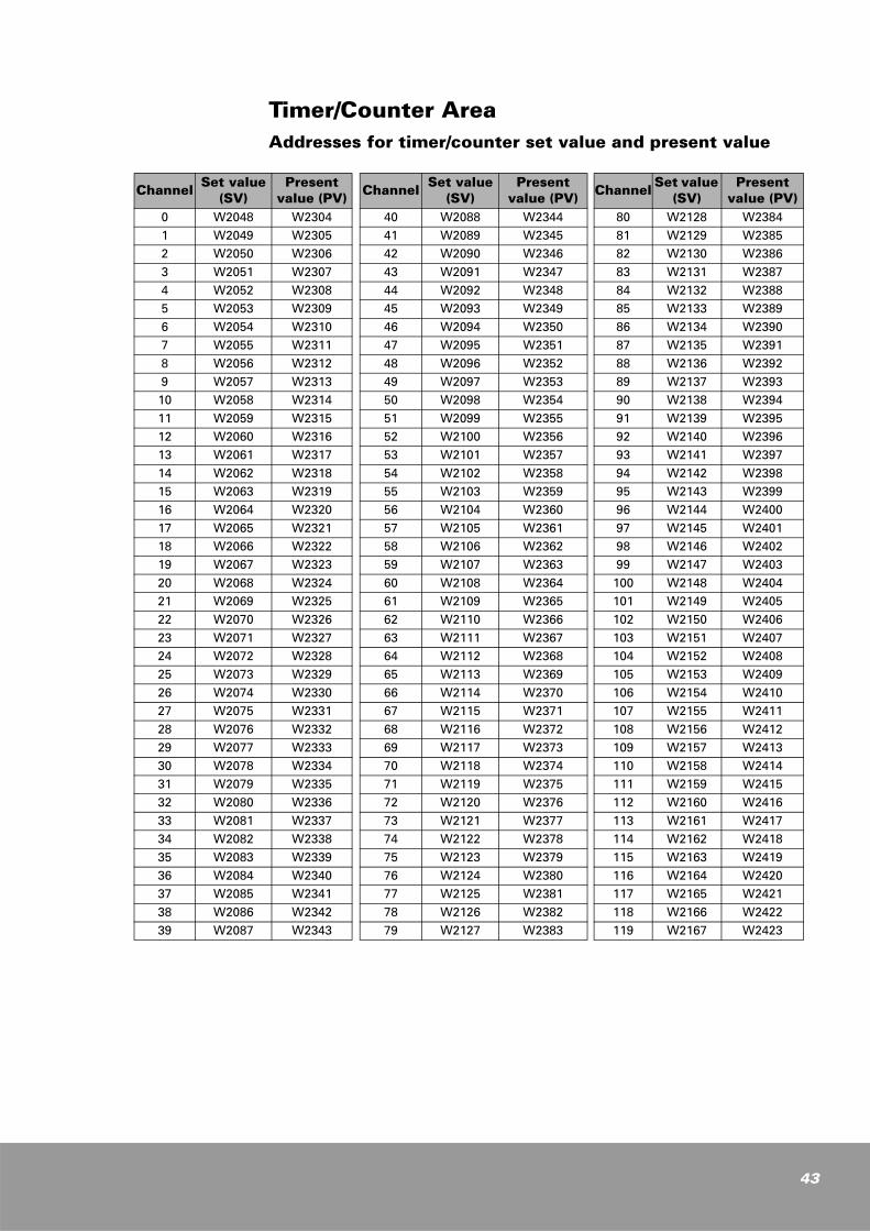
0 W2048 W23041 W2049 W23052 W2050 W23063 W2051 W23074 W2052 W23085 W2053 W23096 W2054 W23107 W2055 W23118 W2056 W23129 W2057 W2313
10 W2058 W231411 W2059 W231512 W2060 W231613 W2061 W231714 W2062 W231815 W2063 W231916 W2064 W232017 W2065 W232118 W2066 W232219 W2067 W232320 W2068 W232421 W2069 W232522 W2070 W232623 W2071 W232724 W2072 W232825 W2073 W232926 W2074 W233027 W2075 W233128 W2076 W233229 W2077 W233330 W2078 W233431 W2079 W233532 W2080 W233633 W2081 W233734 W2082 W233835 W2083 W233936 W2084 W234037 W2085 W234138 W2086 W234239 W2087 W2343
Channel Set value (SV)
Present value (PV)
40 W2088 W234441 W2089 W234542 W2090 W234643 W2091 W234744 W2092 W234845 W2093 W234946 W2094 W235047 W2095 W235148 W2096 W235249 W2097 W235350 W2098 W235451 W2099 W235552 W2100 W235653 W2101 W235754 W2102 W235855 W2103 W235956 W2104 W236057 W2105 W236158 W2106 W236259 W2107 W236360 W2108 W236461 W2109 W236562 W2110 W236663 W2111 W236764 W2112 W236865 W2113 W236966 W2114 W237067 W2115 W237168 W2116 W237269 W2117 W237370 W2118 W237471 W2119 W237572 W2120 W237673 W2121 W237774 W2122 W237875 W2123 W237976 W2124 W238077 W2125 W238178 W2126 W238279 W2127 W2383
Channel Set value (SV)
Present value (PV)
80 W2128 W238481 W2129 W238582 W2130 W238683 W2131 W238784 W2132 W238885 W2133 W238986 W2134 W239087 W2135 W239188 W2136 W239289 W2137 W239390 W2138 W239491 W2139 W239592 W2140 W239693 W2141 W239794 W2142 W239895 W2143 W239996 W2144 W240097 W2145 W240198 W2146 W240299 W2147 W2403
100 W2148 W2404101 W2149 W2405102 W2150 W2406103 W2151 W2407104 W2152 W2408105 W2153 W2409106 W2154 W2410107 W2155 W2411108 W2156 W2412109 W2157 W2413110 W2158 W2414111 W2159 W2415112 W2160 W2416113 W2161 W2417114 W2162 W2418115 W2163 W2419116 W2164 W2420117 W2165 W2421118 W2166 W2422119 W2167 W2423
Timer/Counter AreaAddresses for timer/counter set value and present value
43

44
Addresses for timer/counter set value and present value (Continued)
Channel Set value (SV)
Present value (PV)
120 W2168 W2424121 W2169 W2425122 W2170 W2426123 W2171 W2427124 W2172 W2428125 W2173 W2429126 W2174 W2430127 W2175 W2431128 W2176 W2432129 W2177 W2433130 W2178 W2434131 W2179 W2435132 W2180 W2436133 W2181 W2437134 W2182 W2438135 W2183 W2439136 W2184 W2440137 W2185 W2441138 W2186 W2442139 W2187 W2443140 W2188 W2444141 W2189 W2445142 W2190 W2446143 W2191 W2447144 W2192 W2448145 W2193 W2449146 W2194 W2450147 W2195 W2451148 W2196 W2452149 W2197 W2453150 W2198 W2454151 W2199 W2455152 W2200 W2456153 W2201 W2457154 W2202 W2458155 W2203 W2459156 W2204 W2460157 W2205 W2461158 W2206 W2462159 W2207 W2463159 W2208 W2464160 W2209 W2465161 W2210 W2466162 W2211 W2467163 W2212 W2468164 W2213 W2469
Channel Set value (SV)
Present value (PV)
166 W2214 W2470167 W2215 W2471168 W2216 W2472169 W2217 W2473170 W2218 W2474171 W2219 W2475172 W2220 W2476173 W2221 W2477174 W2222 W2478175 W2223 W2479176 W2224 W2480177 W2225 W2481178 W2226 W2482179 W2227 W2483180 W2228 W2484181 W2229 W2485182 W2230 W2486183 W2231 W2487184 W2232 W2488185 W2233 W2489186 W2234 W2490187 W2235 W2491188 W2236 W2492189 W2237 W2493190 W2238 W2494191 W2239 W2495192 W2240 W2496193 W2241 W2497194 W2242 W2498195 W2243 W2499196 W2244 W2500197 W2245 W2501198 W2246 W2502199 W2247 W2503200 W2248 W2504201 W2249 W2505202 W2250 W2506203 W2251 W2507204 W2252 W2508205 W2253 W2509206 W2254 W2510207 W2255 W2511208 W2256 W2512209 W2257 W2513210 W2258 W2514211 W2259 W2515
Channel Set value (SV)
Present value (PV)
212 W2260 W2516213 W2261 W2517214 W2262 W2518215 W2263 W2519216 W2264 W2520217 W2265 W2521218 W2266 W2522219 W2267 W2523220 W2268 W2524221 W2269 W2525222 W2270 W2526223 W2271 W2527224 W2272 W2528225 W2273 W2529226 W2274 W2530227 W2275 W2531228 W2276 W2532229 W2277 W2533230 W2278 W2534231 W2279 W2535232 W2280 W2536233 W2281 W2537234 W2282 W2538235 W2283 W2539236 W2284 W2540237 W2285 W2541238 W2286 W2542239 W2287 W2543240 W2288 W2544241 W2289 W2545242 W2290 W2546243 W2291 W2747244 W2292 W2548245 W2293 W2549246 W2294 W2550247 W2295 W2551248 W2296 W2552249 W2297 W2553250 W2298 W2554251 W2299 W2555252 W2300 W2556253 W2301 W2557254 W2302 W2558255 W2303 W2559

Absolute AddressingIn LDR, DLDR, STO, and DSTO instructions, the absolute address is used to perform indirect addressing to register or utilize the built-in communication port.
When accessing a bit absolute address using the program loader port communication protocol, the bit address (0 to 15 or $0 to $F) is kept separate from the word address (as shown below).
For example, the absolute bit address for K12712 internal contact is $1BFC (hex). (Word absolute address = $01BF + Bit number = $C = $1BFC)
Bit numberWord absolute address1 word display15 4 3 0
Memory area
Register address
Absolute address
Dec. Hex.
Special internal contact
F0000 448 01C0
F0001 449 01C1
F0002 450 01C2
... ... ...
F0126 462 01CE
F0127 462 01CF
Data area
W0000 512 0200
W0001 513 0201
W0002 514 0202
... ... ...
W512 1024 0400
... ... ...
W1024 1536 0600
... ... ...
W1536 2048 0800
... ... ...
W2046 2558 09FE
W2047 2559 09FF
T/Cset value
W2048 2560 0A00
W2049 2561 0A01
... ... ...
W2303 2815 0AFF
T/Cpresent value
W2304 2816 0B00
W2305 2817 0B01
... ... ...
W2559 3071 0BFF
Statusdisplay
W2560 3072 0C00
W2561 3073 0C01
... ... ...
W2564 3583 0DFF
Memory area
Register address
Absolute address
Dec. Hex.
External I/O
R0000 0 0000
R0001 1 0001
R0002 2 0002
... ... ...
R0126 126 007E
R0127 127 007F
Link area
L0000 128 0080
L0001 129 0081
L0002 130 0082
... ... ...
L0062 190 00BE
L0063 191 00BF
Internal contact
M0000 192 00C0
M0001 192 00C1
M0002 194 00C2
M0003 195 00C3
... ... ...
M0064 256 0100
M0065 257 0101
... ... ...
M0126 318 013E
M0127 319 013F
Internal Keep contact
K0000 320 0140
K0001 321 0141
K0002 322 0142
K0003 323 0143
... ... ...
K0126 446 01BE
K0127 447 01BF
45

46
Processor Operation ModeWhat is the processor operation mode?
The processor has an external RUN/REMOTE/PROG switch. The PLC performs a system check that determines the position of the switch. The switch position determines which operating mode the PLC is in. It can set to RUN, STOP, REMOTE, or ERROR mode.
Processor operation modes
LED status - : On, : Flashing, : OffWhen the PROG.LED is on, you can change the user program
When the mode switch is set to REMOTE and power is switched from Off to On, the previous mode of operation is restored.
When debugging the user program, the mode switch should be set to REMOTE.
Operation mode selector switch
Operation mode
LED status Program change
Data change
Operation mode at power off to onRUN PROG
RUNRUN Disabled Enabled RUN
STOP Disabled Enabled RUN
RMT (REMOTE)RUN Enabled Enabled RUN
PAUSE Enabled Enabled PAUSE
PROG STOP Enabled Enabled STOP
Status LEDs
Operation mode selector
IMPORTANT

Changes of operation mode according to operation mode selector switch position
As in the status indicator, if an error occurs within a mode during RUN state, set the mode change to STOP or PAUSE automatically base on the type of error information, and the error lamp is turned on. However, an arithmetic error will occur during the operation when, the error lamp is turned on and is changed to STOP. Afterwards, after the PROCESSOR has been halted, the error lamp may be turned off.
Mode switches in status will be remotely changed when the error is canceled.
Be cautious during programming since the status switch of Note 1) or Note 2) changes even when setting the F0.15 contact that controls operation modes is turned to On/Off.
Note2
The PLC reads the external input signals and executes the user program stored in memory. The external outputs are updated on every scan based on program results. (Run LED maintains On.)
A user program is operated at every scan and the I/O and result value is maintained. This mode is used when checking and debugging a program at every scan. This mode is similar to the Stop mode, but it does not initialize data. (RUN LED flickers.)
The user program is stopped and the external outputs are turned Off. In the Stop mode, you may correct, delete or transfer the program.
The ERROR mode occurs when the PLC finds an error after running the self-diagnosis routine. When an error occurs, the PROCESSOR decides whether the operation continues, and displays either STOP or RUN. The Error can be cleared by changing the power from Off to On, switching operation mode from STOP to RUN, or downloading programs after checking the error code and taking the appropriate measures.
Switch position Operation mode change
RUN
RMT
PROG
PAUSE Mode
STOP Mode
ERROR Mode
RUN Mode
NOTE1
NOTE2
NOTE3
PAUSE
RUN
RUN
STOP
47

48
( )
5
Programming Instructions
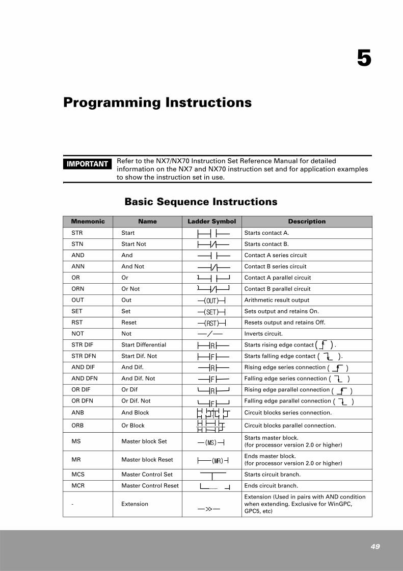
Refer to the NX7/NX70 Instruction Set Reference Manual for detailed information on the NX7 and NX70 instruction set and for application examples to show the instruction set in use.
Basic Sequence Instructions
Mnemonic Name Ladder Symbol Description
STR Start Starts contact A.
STN Start Not Starts contact B.
AND And Contact A series circuit
ANN And Not Contact B series circuit
OR Or Contact A parallel circuit
ORN Or Not Contact B parallel circuit
OUT Out Arithmetic result output
SET Set Sets output and retains On.
RST Reset Resets output and retains Off.
NOT Not Inverts circuit.
STR DIF Start Differential Starts rising edge contact .
STR DFN Start Dif. Not Starts falling edge contact .
AND DIF And Dif. Rising edge series connection
AND DFN And Dif. Not Falling edge series connection
OR DIF Or Dif Rising edge parallel connection
OR DFN Or Dif. Not Falling edge parallel connection
ANB And Block Circuit blocks series connection.
ORB Or Block Circuit blocks parallel connection.
MS Master block SetStarts master block.(for processor version 2.0 or higher)
MR Master block ResetEnds master block.(for processor version 2.0 or higher)
MCS Master Control Set Starts circuit branch.
MCR Master Control Reset Ends circuit branch.
- ExtensionExtension (Used in pairs with AND condition when extending. Exclusive for WinGPC, GPC5, etc)
( )( )
( )( )
( )
(OUT)
(SET)
(RST)
R
F
R
F
R
F
(MS)
(MR)
>>
IMPORTANT
49

50
Timer, Counter and Shift Register Instructions
Mnemonic Name Ladder Symbol Description Remarks
TIM On Delay Timer
Turns on after set delay time from input on
Time base: Ch 0 to 63 = 0.01sCh 64 to 255 = 0.1s
Setting range: SV = 0 to 65535
Contact indicator: TC + channel number
TOF Off Delay Timer
Turns off after set delay time from input off
Time base: Ch 0 to 63 = 0.01sCh 64 to 255 = 0.1s
Setting range: SV = 0 to 65535
Contact indicator: TC + channel number
SSTSingle Shot
Timer
Turns off after set delay time from input on
Time base: Ch 0 to 63 = 0.01sCh 64 to 255 = 0.1s
Setting range: SV = 0 to 65535
Contact indicator: TC + channel number
UCUp Counter
Up counter Channel range: Ch 0 to 255
(Shared with timer)
Setting range: SV = 0 to 65535
Contact indicator: TC + channel number
DC Down Counter
Down counter Channel range: Ch 0 to 255
(Shared with timer)
Setting range: SV = 0 to 65535
Contact indicator: TC + channel number
RCT Ring Counter
Ring counter Channel range: Ch 0 to 255
(Shared with timer)
Setting range: SV = 0 to 65535
Contact indicator: TC + channel number
UDCUp-Down Counter
Up-Down counter Channel range: Ch 0 to 255
(Shared with timer)
Setting range: SV = 0 to 65535
Contact indicator: TC + channel number
SR Shift Register
Shift Register Usable address areas for Sb and Eb: M, K
1 bit shift on each p input.
Stores the status value I in Sb for every P input.
Max. number of instructions: 256
TIM
Ch=00010
SV=00050
TOF
Ch=00064
SV=00005
SST
Ch=00100
SV=00005
UC
U Ch=020
SV=004
R
DC
D Ch=021
SV=005
R
RCT
T Ch=022
SV=004
R
UDC
U Ch=023
SV=003
D
R
SR
I Sb=K1.4
Eb=K2.5
P
R
← 5 s e c →
In p ut
o u tpu t
In p ut
o u tpu t ← 5 s e c →
← 5 s e c →
In p ut
o u tpu t
In p ut
C u rre nt va lue
Ou tp u t
R e se t
S e t v a lu e
In p ut
C u rre ntva lueOu tp u t
R e se t
S e t v a lu e
In p ut
C u rre ntva lueOu tp u t
R e se t
S e t v a lu e
D In p ut
C u rre ntva lue
Ou tp u tR e se t
S e t v a lu e
U In p ut
S b
E b
K1.4
...
...
K2.5
.
...
.
II=v a lu e

Comparison Instructions
For double word comparison instructions, the letter D should precede the word comparison instructions in the Mnemonic program.
Substitution, Increment and Decrement Instructions
Mnemonic Name Word ladder symbol
Double word ladder symbol Description
STR ==
AND ==
OR ==
START ==
AND ==
OR ==
On if A is equal to B.
A and B are word/double word or data value.
STR <>
AND <>
OR <>
START <>
AND <>
OR <>
On if A is not equal to B.
<> is same with ≠ .
A and B are word/double word or data value
STR >
AND >
OR >
START >
AND >
OR >
On if A is greater than B.
STR >=
AND >=
OR >=
START >=
AND >=
OR >=
On if A is equal to or greater than B.
STR <=
AND <=
OR <=
START <=
AND <=
OR <=
On if A is equal to or less than B.
STR <
AND <
OR <
START <
AND <
OR <
On if A is less than B.
Mnemonic Name Word ladder symbol
Double word ladder symbol Description
LET(DLET)
Let (Substitution)
Store the value of S into D.
INC(DINC)
Decimal incrementIncrement D by 1 whenever input goes on.
INCB (DINCB)
BCD increment Increment D by 1 in BCD mode whenever input goes on.
DEC (DDEC)
Decimal decrement Decrement D by 1 whenever input goes on.
DECB (DDECB)
BCD decrement Decrement D by 1 in BCD mode whenever input goes on.
==
A=
B=
<>
A=
B=
>
A=
B=
>=
A=
B=
<=
A=
B=
<
A=
B=
D==
A=
B=
D<>
A=
B=
D>
A=
B=
D>=
A=
B=
D<=
A=
B=
D<
A=
B=
IMPORTANT
51
52
Arithmetic Instructions
Mnemonic Name Word ladder symbol
Double word ladder symbol Description
ADD
(DADD)
Decimal
addition
D = S1 + S2
(Decimal operation)
ADDB
(DADDB)BCD addition
D = S1 + S2
(BCD operation)
SUB
(DSUB)Decimal subtraction
D = S1 - S2
(Decimal operation)
SUBB
(DSUBB)BCD subtraction
D = S1 - S2
(BCD operation)
MUL
(DMUL)Decimal multiplication
D = S1 x S2
(Decimal operation)
MULB
(DMULB)BCD multiplication
D = S1 x S2
(BCD operation)
DIV
(DDIV)Decimal division
D = S1/S2 (Decimal operation),
Error when S2= 0
DIVB
(DDIVB)BCD division
D = S1/S2 (BCD operation)
Error when S2 = 0
ADC
(DADC)Decimal addition with carry
D = S1 + S2 + CY
(Decimal operation, include carry)
ADCB
(DADCB)BCD addition with carry
D = S1 + S2 + CY
(BCD operation, include carry)
SBC
(DSBC)
Decimal subtraction with carry
D = S1 - S2 – CY
(Decimal operation, include carry)
SBCB
(DSBCB)BCD subtraction with carry
D = S1 - S2 - CY
(BCD operation, include carry)
ABS
(DABS)Absolute value
D = |D|
(Absolute value operation)
WNOT
(DNOT)
NOT
(1’s complement)Store 1’s complement of D in D
NEG
(DNEG)
Negative
(2’s complement)
Store 2’s complement of D in D
(1’s complement + 1) (- Result)

Logical Instructions
Rotation Instructions
Mnemonic Name Word ladder symbol
Double word ladder symbol Description
WAND (DAND)
AND (logical multiply)
Store AND of S1 and S2 in D
WOR(DOR)
OR (logical sum)
Store OR of S1 and S2 in D
WXOR (DXOR)
Exclusive OR (exclusive logical sum)
Store exclusive OR of S1 and S2 in D
WXNR (DXNR)
Exclusive OR NOT (equivalence)
Store exclusive OR NOT of S1 and S2 in D 1 (ON if they are equal)
Mnemonic Instruction Word ladder symbol
Double word ladder symbol Description
RLC (DRLC)
Rotate left without carry
Rotate the content of D to the left N times. (lower->higher)
RRC (DRRC)
Rotates right without carry
Rotate the content of D to the right N times (higher->lower)
ROL (DROL)
Rotate left with carry
Rotate (shift) to the left N times(Input F1.8 value to the lowest bit)
ROR (DROR)
Rotate right with carry
Rotate (shift) to the right N times(higher->lower)(Input F1.8 value to the highest bit)
SHL(DSHL)
Shift leftShift the content of D to the left N times (input 0 to the lowest bit)
SHR (DSHR)
Shift rightShift the content of D to the right N times (input 0 to the highest bit)
53

54
Word Conversion Instructions
Mnemonic Name Word ladder symbol
Double word ladder symbol Description
BCD (DBCD)
BCD Conversion
Convert binary value of S to BCD and store it in D.
BIN(DBIN)
Binary Conversion
Convert BCD of S to binary number and store it in D.
ENCO Encode
Store the location of the highest set bit in S in D.
DECO Decode
Convert the low-order 4-bit value of S to a power of 2 (2s) and store it in D.
SEG 7-Segment
Converts the low-order 4-bit value of S to 7-segment display pattern and store them in D.
XCHG (DXCHG)
Exchange
Exchange D1 and D2 values.
DIS Dissemble
Separate S into N+1 units, 4 bits each, and store them in the low 4 bits of words starting at D.
UNI Unify
Combine the low 4 bits of S+1 words starting at S, and store them in D (N= 0 to 3).
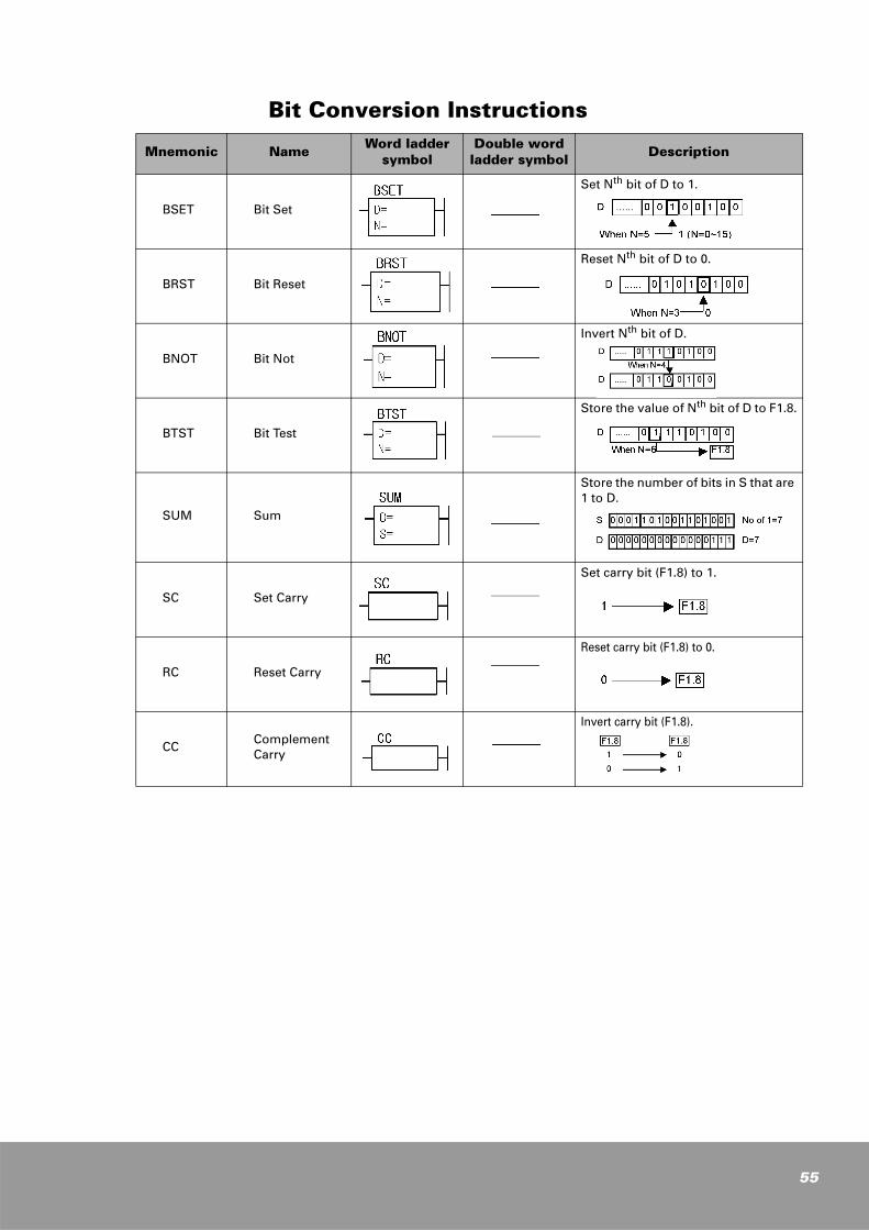
Bit Conversion Instructions
Mnemonic Name Word ladder symbol
Double word ladder symbol Description
BSET Bit Set
Set Nth bit of D to 1.
BRST Bit Reset
Reset Nth bit of D to 0.
BNOT Bit Not
Invert Nth bit of D.
BTST Bit Test
Store the value of Nth bit of D to F1.8.
SUM Sum
Store the number of bits in S that are 1 to D.
SC Set Carry
Set carry bit (F1.8) to 1.
RC Reset Carry
Reset carry bit (F1.8) to 0.
CCComplement Carry
Invert carry bit (F1.8).
55

56
Move Instructions
Mnemonic Name Word ladder symbol
Double word ladder symbol Description
MOV Move
Copy Ns words from Sr to D.
FMOV Fill Move
Repeatedly copy the value V to the Ns words starting from D.
BMOV Bit Move
Move Ns bits from the bit address Sb to the bit address Db.
BFMV Bit Fill Move
Repeatedly copy the bit value V to the N bits staring from the bit address Db. (V=0, 1)(N=1…256)(Db is bit address)
LDR (DLDR)
Load D ← (S)
Store to D the value of the register whose absolute address is the value of S. (Refer to the manual for information about absolute address.)
STO (DSTO)
Store (D) ← S
Store the value of S to the register whose absolute address is the value of D.
(Refer to the manual for information about absolute address.)
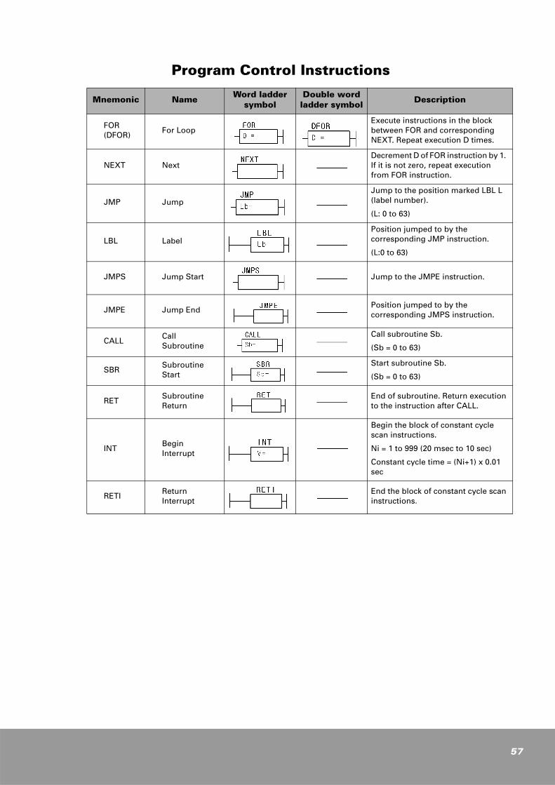
Program Control Instructions
Mnemonic Name Word ladder symbol
Double word ladder symbol Description
FOR (DFOR)
For LoopExecute instructions in the block between FOR and corresponding NEXT. Repeat execution D times.
NEXT NextDecrement D of FOR instruction by 1. If it is not zero, repeat execution from FOR instruction.
JMP JumpJump to the position marked LBL L (label number).
(L: 0 to 63)
LBL LabelPosition jumped to by the corresponding JMP instruction.
(L:0 to 63)
JMPS Jump Start Jump to the JMPE instruction.
JMPE Jump EndPosition jumped to by the corresponding JMPS instruction.
CALLCall Subroutine
Call subroutine Sb.
(Sb = 0 to 63)
SBRSubroutine Start
Start subroutine Sb.
(Sb = 0 to 63)
RETSubroutine Return
End of subroutine. Return execution to the instruction after CALL.
INTBegin Interrupt
Begin the block of constant cycle scan instructions.
Ni = 1 to 999 (20 msec to 10 sec)
Constant cycle time = (Ni+1) x 0.01 sec
RETIReturn Interrupt
End the block of constant cycle scan instructions.
57
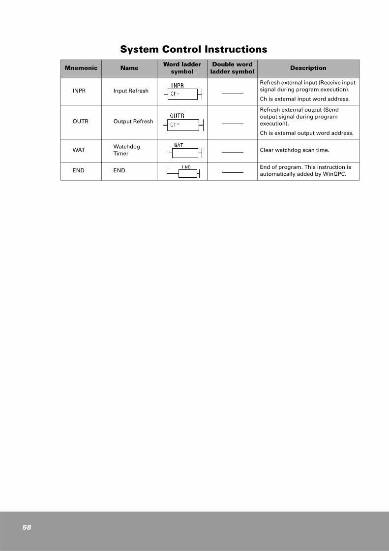
58
System Control Instructions
Mnemonic Name Word ladder symbol
Double word ladder symbol Description
INPR Input RefreshRefresh external input (Receive input signal during program execution).
Ch is external input word address.
OUTR Output Refresh
Refresh external output (Send output signal during program execution).
Ch is external output word address.
WATWatchdog Timer
Clear watchdog scan time.
END ENDEnd of program. This instruction is automatically added by WinGPC.
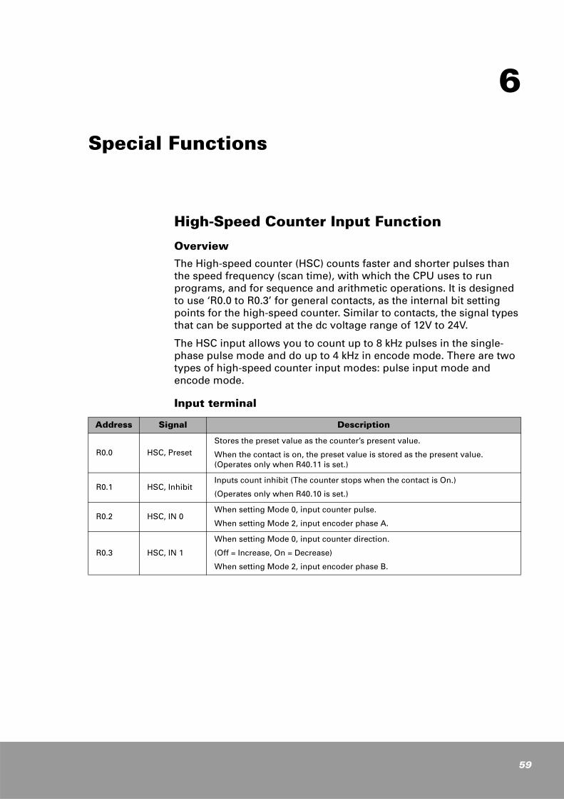
6Special Functions
High-Speed Counter Input Function
Overview
The High-speed counter (HSC) counts faster and shorter pulses than the speed frequency (scan time), with which the CPU uses to run programs, and for sequence and arithmetic operations. It is designed to use ‘R0.0 to R0.3’ for general contacts, as the internal bit setting points for the high-speed counter. Similar to contacts, the signal types that can be supported at the dc voltage range of 12V to 24V.
The HSC input allows you to count up to 8 kHz pulses in the single-phase pulse mode and do up to 4 kHz in encode mode. There are two types of high-speed counter input modes: pulse input mode and encode mode.
Input terminal
Address Signal Description
R0.0 HSC, PresetStores the preset value as the counter’s present value.
When the contact is on, the preset value is stored as the present value. (Operates only when R40.11 is set.)
R0.1 HSC, InhibitInputs count inhibit (The counter stops when the contact is On.)
(Operates only when R40.10 is set.)
R0.2 HSC, IN 0When setting Mode 0, input counter pulse.
When setting Mode 2, input encoder phase A.
R0.3 HSC, IN 1
When setting Mode 0, input counter direction.
(Off = Increase, On = Decrease)
When setting Mode 2, input encoder phase B.
59

60
High-speed counter registers
Address Signal Description
R40 High-speed counter mode setting
R41 - Reserved
R42 CH0 PV_LO Stores the counter present value, low word (low 16 bits)
R43 CH0 PV_HI Stores the counter present value, high word (high 16 bits)
R44 CH0 STR_LO Stores the preset value (low word)
R45 CH0 STR_HI Stores the preset value (high word)
R46 ~ 55 - Reserved
R56 H0 SV_LO Stores the set value (low word)
R57 H0 SV_HI Stores the set value (high word)
R58 - Reserved
R59 - Reserved
R60CH0 CATCH_LO
Stores the present value (low word) at the point of inputting the preset (H0 PV_LO)
R61CH0 CATCH_HI
Stores the present value (high word) at the point of inputting the preset (H0 PV_HI)
R62~64 - Reserved
Address Signal Description
R65.0 HSC Enable Sets the operation of high-speed counter ('1' = enable, '0' = disable)
R65.1 - Reserved
R65.2 HSC Start Sets the counting of counter ('1' = enable, '0' = disable)
R65.3 - Reserved
R65.4~5 - Reserved
R65.6 Ring Counter Sets ring counter mode ('1' = enable, '0' = disable)
R65.7 - Reserved
15 14 13 12 11 10 9 8 7 6 5 4 3 2 1 0Bit no.
Reserved
Sets software preset function
Sets the use of R0.3 (input direction/phase B)
Sets the use of R0.2 (input pulse/phase A)
Sets the use of R0.1 (input count inhibit)
= Sets mode 0= pulse input mode (input R0.2 = pulse, R0.3 = direction)
= Sets mode 2= encode mode (input R0.2 = phase A, R0.3 = phase B)
Sets ring counter (input '1' = Enable,'0' = Disable)
Indicates the RUN/STOP status of HSC (display On when HSC is operating)
0 0
Sets the use of R0.0 (input preset)
1 0

Pulse input mode (Mode 0)
The pulse input mode is executed by setting the contacts R40.13 and R40.12 to ‘0’. It counts input pulses that enter the R0.2 input terminal. The counter value increases when the R0.3 terminal signal that determines the direction is set to Off, and it decreases when the R0.3 terminal signal is set to On. If the bit of the direction setting input R40.8 is set to Off (set as '0'), then the count will always increase.
Address and setting for pulse input mode
Address and setting for I/O
Address Setting Description
R65.0 1 Sets the operation of high-speed counter ('1' = enable, '0' = disable)
R65.2 1 Sets the counting of counter ('1' = enable, '0' = disable)
0 0 0 0 1 1 1 1 0 0 0 0 0 0 0
Address Setting Description
R0.0 1 Stores the preset as the counter’s present value (Operates at a rising edge)
R0.1 1 Inputs count inhibit (The counter stops when the contact is On.)
R0.2 1 When setting Mode 0 (pulse input mode), inputs counter pulse.
R0.3 1When setting Mode 0 (pulse input), inputs counter direction (Off = Increase, On = Decrease)
Word R40 Bit no.
ReservedSets the use of R0.3 (input direction)(input 1= Increase/decrease mode, 0=Increase mode)
Sets the use of R0.2 (input pulse)
Sets the use of R0.1 (input count inhibit)
Sets the use of R0.0 (input preset)
=Sets mode 0= pulse input mode (input R0.2 = pulse, R0.3 = direction)
Sets ring counter (input '1' = enable, '0' = disable)
Indicates the Run/Stop status of HSC (display On when HSC is operating)
0 0
15 14 13 12 11 10 9 8 7 6 5 4 3 2 1
61

62
Counting graph in pulse input mode
In the case of the pulse input mode, the HSC performs counting when a pulse is falling. The present value of the counter is scaled up when the direction input is Off, and is scaled down when the direction input is On.
When the counter inhibit input is set to On, the counter stops counting regardless of the direction.
Example of pulse input mode wiring
Pulse input(R0.2)
Direction input(R0.3)
Counting inhibit(R0.1)
PV value
Forward direction Reserve direction
Counter runs
Forward direction
Counter inhibit
Directio
n in
pu
t
Pu
lse inp
ut
Co
un
t inh
ibit in
pu
t
Preset valu
e storag
e
For 28 and 48 points
High Speed counter input terminal
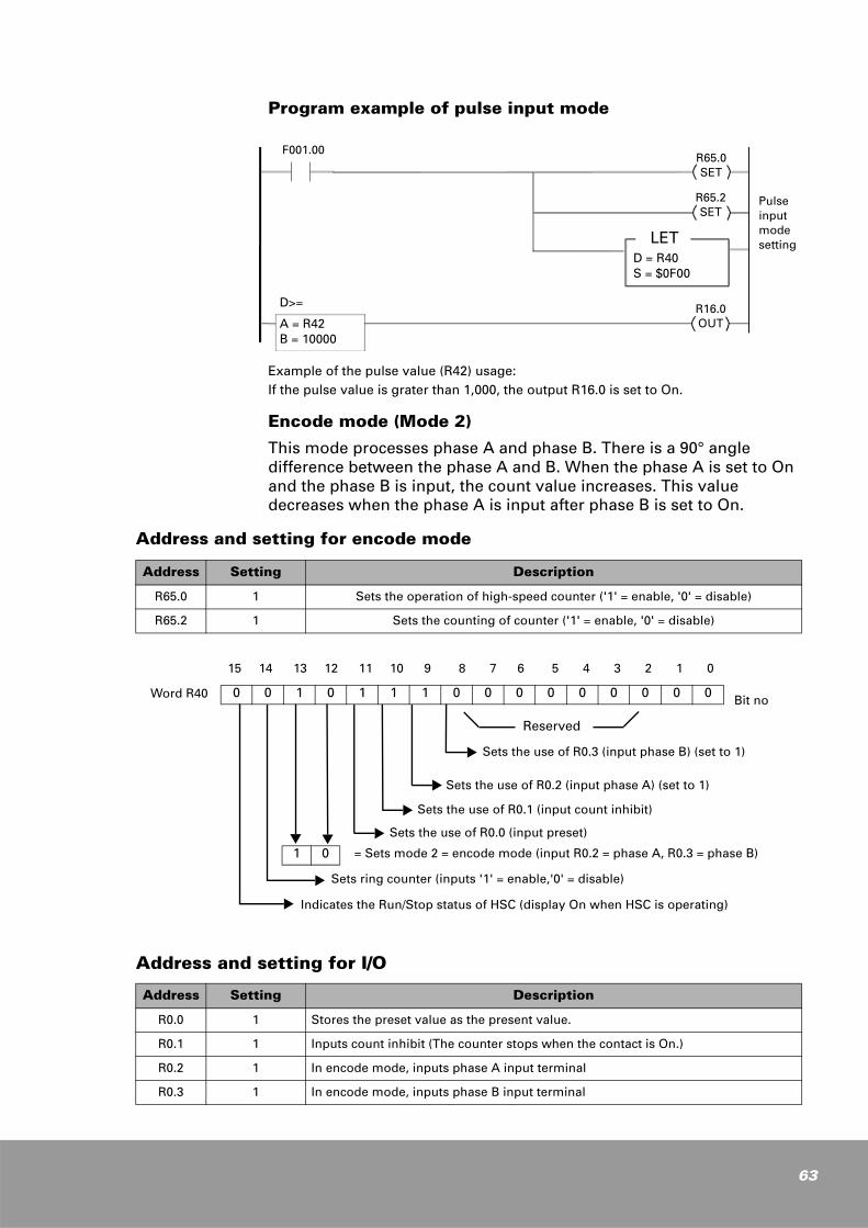
Program example of pulse input mode
Example of the pulse value (R42) usage:If the pulse value is grater than 1,000, the output R16.0 is set to On.
Encode mode (Mode 2)
This mode processes phase A and phase B. There is a 90° angle difference between the phase A and B. When the phase A is set to On and the phase B is input, the count value increases. This value decreases when the phase A is input after phase B is set to On.
Address and setting for encode mode
Address and setting for I/O
Address Setting Description
R65.0 1 Sets the operation of high-speed counter ('1' = enable, '0' = disable)
R65.2 1 Sets the counting of counter ('1' = enable, '0' = disable)
Address Setting Description
R0.0 1 Stores the preset value as the present value.
R0.1 1 Inputs count inhibit (The counter stops when the contact is On.)
R0.2 1 In encode mode, inputs phase A input terminal
R0.3 1 In encode mode, inputs phase B input terminal
Word R40 Bit no
Reserved
Sets the use of R0.3 (input phase B) (set to 1)
Sets the use of R0.2 (input phase A) (set to 1)
Sets the use of R0.1 (input count inhibit)
Sets the use of R0.0 (input preset)
= Sets mode 2 = encode mode (input R0.2 = phase A, R0.3 = phase B)
Sets ring counter (inputs '1' = enable,'0' = disable)
Indicates the Run/Stop status of HSC (display On when HSC is operating)
1 0
15 14 13 12 11 10 9 8 7 6 5 4 3 2 1 0
0 0 1 0 1 1 1 0 0 0 0 0 0 0 0 0
F001.00R65.0SET
R65.2SET
LETD = R40S = $0F00
R16.0OUTA = R42
B = 10000
D>=
Pulse input mode setting
63

64
Counting graph in encode mode (two-phase input)
The present value of the counter is going up when the phase angle of phase A is followed by that of phase B, while B is going down, and when phase B is followed by phase A. Essentially, when the phase A value is input first, the count increases as the phase A value rises (incremental edge), but when the phase A value is input later, the count decreases as the phase A value falls (decremented edge).
Example of encode mode wiring
Program example of encode input mode
Example of the pulse value (R42) usage:If the pulse value is between 1,000 and 2,000, the output R16.0 is set to On.
24Vencoder
+V OV A BFor 28 and 48 points
High-speed counter input terminal
Phase A
Phase B
PV
Encoder direction switching
F001.00
D>=
A = R42B = 10000
D<
A = R42B = 20000
R65.0SET
R65.2SET
LETD = R40S = $2F00
R16.0OUT
Encodeinput mode setting

Input Pulse Catch Function
Overview
Four input contacts (R0.0, R0.1, R0.4, and R0.5) have a pulse catch function, which maintains the On status until the scan is completed, even when a shorter pulse than the scan time is input. This function allows these contacts to process the high-speed pulses, which are shorter than the scan time, and without the additional cost.
Address settings
Time chart
Program example of pulse catch function
Address Signal Description
R66.0 P_CATCH_0 Sets the use of R0.0 pulse catch function ('1' = enable, '0' = disable)
R66.1 P_CATCH_1 Sets the use of R0.1 pulse catch function ('1' = enable, '0' = disable)
R66.4 P_CATCH_4 Sets the use of R0.4 pulse catch function ('1' = enable, '0' = disable)
R66.5 P_CATCH_5 Sets the use of R0.5 pulse catch function ('1' = enable, '0' = disable)
Inputupdate
Program executionOutputupdate
OtherInputupdate
Program executionOutputupdate
Other
Scan time
PLC scan
Pulse input
Pulse catch process
400 µs or more
Maintains it till the input update
R0.0 pulse catch function setting
R0.1 pulse catch function setting
R0.4 pulse catch function setting
R0.5 pulse catch function setting
< SET >
< SET >
Operates the first one scan at the beginning
F001.00R66.0
R66.4
R66.5
< SET >
< SET >R66.1
65

66
Pulse Output Function (for Transistor Output Model)
Pulse output settings registers
Pulse acceleration/deceleration designation area (supports version 1.20 or higher in pulse mode)
Address Signal Description
R32Pulse outputChannel 0Mode setting
R33 CH0 FREQ.* Sets pulse output frequency
- Output frequency: 20 to 5,000 Hz
R34CH0 DUTY orCH0 SV (Pulse numbers)
* Sets pulse output duty ratio or output pulse numbers
- For PWM mode, sets duty ratio (25% to 75%)
- For Pulse + Dir, sets output pulse numbers
R35 CH0 PV Indicates the number of pulses from channel 0
R36Pulse outputChannel 1Mode setting
R37 CH1 FREQ.* Sets pulse output frequency
- Output frequency: 20 to 5,000 Hz
R38
CH1 DUTY orCH0 SV (Number of pulses)
* Sets pulse output duty ratio or output pulse numbers
- For PWM mode, sets duty ratio (25% to 75%)
- For Pulse + Dir, sets output pulse numbers
R39 CH1 PV Indicates the number of pulses from channel 1
15 14 13 12 11 10 9 8 7 6 5 4 3 2 1 0Bit no
Reserved
Reserved
= Sets direction mode = pulse (R16.0) + direction (R16.2) mode
= Sets PWM mode = PWM pulse output (R16.0) + direction (R16.2)
ReservedIndicates Run/Stop of pulse output (display On when the pulse output is operating)
0 0
Controls R16.2 direction mode output (use 1 = high, 0 = low)
Sets the use of R16.2 output direction(use 1 = direction output, 0 = general contact)
Pulse output channel 0, control register
1 1
1
15 14 13 12 11 10 9 8 7 6 5 4 3 2 1 0Bit no
Reserved
Reserved
= Sets direction mode = pulse (R16.1) + direction (R16.3) mode
= Sets PWM mode = PWM pulse output (R16.1) + direction (R16.3)
Reserved
Indicates RUN/STOP status of pulse output (display On when the pulse output is operating)
0 0
Sets the use of R16.3 direction output(use 1 = direction output, 0 = general contact)
Pulse output channel 1, control register
1 1
1
Controls R16.3 direction mode output (use 1 = high, 0 = low)
NOTE

Bits for pulse output control
Address Signal Description
R67Start frequency for CH0
Area designating start frequency value (when designating acceleration/deceleration pulse of pulse mode)
R68Number of increased pulse for CH0
Designates the number of counter (pulse) in acceleration area
R69Number of decreased pulse for CH0
Designates the number of counter (pulse) in deceleration area
R70Start frequency for CH1
Area designating start frequency value (when designating acceleration/deceleration pulse of pulse mode)
R71Number of increased pulse for CH1
Designates the number of counter (pulse) in the acceleration area
R72Number of decreased pulse for CH1
Designates the number of counter (pulse) in the deceleration area
Address Signal Description
R16.0 CH0_PLS Channel 0 pulse output signal
R16.1 CH1_PLS Channel 1 pulse output signal
R16.2 CH0_DIR Channel 0 direction output signal (enabled when R32.8 contact is '1')
R16.3 CH1_DIR Channel 1 direction output signal (enabled when R32.8 contact is '1')
R64.0 PLS 0_ENDetermines the use of pulse output (CH0) function (1 = for pulse, 0 = for contact point)
R64.1 PLS 1_ENDetermines the use of pulse output (CH1) function (1= for pulse, 0 = for contact point)
R64.2 PULSE_CH0_START Determines whether channel 0 pulse output starts (1 = START, 0 = STOP)
R64.3 PULSE_CH1_START Determines whether channel 1 pulse output starts (1 = START, 0 = STOP)
67

68
How to Use
The pulse output generates output pulses in the following order and process.
1) Set mode setting, direction, frequency, duty ratio, or output numbers in the register.
Ex) In case of CH0, PWM mode, 5 kHz, and 50% duty ratio
- P0 MODE (R32) = $3300 (0011 0011 0000 0000)
- P0 FREQ (R33) = 5000
- P0 DUTY (R34) = 50
2) Set R64.0 to Set ('1') in order to generate pulses as CH0.
3) Set R64.2 to Set ('1') in order for CH0 to start pulse output.
=> When setting is as described above, a PWM signal of 5 kHz goes to CH0.
Program example 1: PWM mode
If you set CH0, PWM mode, 5 kHz, and 50% duty ratio as described above, and output the pulse at 0.5 seconds per second, the following setting is required.
< SET >
F001.00R64.0
D= R32S = $3300
LET
D = R33S = 5000
LET
D = R34S = 50
LET
< OUT >
F001.04R64.2
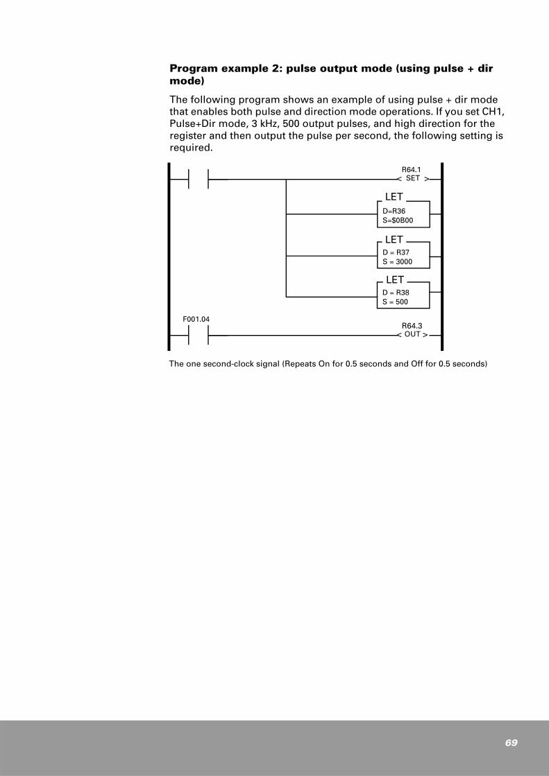
Program example 2: pulse output mode (using pulse + dir mode)
The following program shows an example of using pulse + dir mode that enables both pulse and direction mode operations. If you set CH1, Pulse+Dir mode, 3 kHz, 500 output pulses, and high direction for the register and then output the pulse per second, the following setting is required.
< SET >R64.1
D = R37S = 3000
LET
D = R38S = 500
LET
< OUT >
F001.04R64.3
The one second-clock signal (Repeats On for 0.5 seconds and Off for 0.5 seconds)
D=R36S=$0B00
LET
69

70
Program example 3: pulse output mode (with acceleration/deceleration for version 1.20 or higher)
If you set CH1, pulse mode, 3 kHz, 5,000 output pulses, 500 kHz of start frequency, 1,000 acceleration pulses, 800 deceleration pulses, and high direction in the register and then output the pulse per three seconds, the following setting is required.
< SET >R64.1
D = R36S = $0B00
LET
D = R37S = 3000
LET
D = R38S = 5000
LET
< OUT >
TC000R64.3
D = R70S = 500
LET
D = R71S = 1000
LET
D = R72S = 800
LET
CH = 0SV= 300
TIM
F001.00
F000.15 TC000

Appendix
Using WinGPC
Wiring and Switch SettingsAn example of RS-232C communications between PC and PLC
PLC (NX7)(Modular jack)
1
TXDRXD
RXD
TXD3
4
5
6
7
8
9
8
6
9-pin D-Sub connector (Female) 8-pin modular connector
PC
PC
RXD 2
TXD 3
DTR 4
GND 5
DSR 6
RTS 7
CTS 8
- 9
PLC (NX7)
2 TXD
3 RXD
4 RTS
5 GND
6 485-
7 485+
8 CTS
9 Vcc
9-pin D-Sub connector(Female) 9-pin D-Sub connector
(Male)
PLC FG (CASE)
PC setting (Ex: WinGPC)
- PC communication port setting (COM1 to 4)
- Communication speed (38400 to 4800)
- No access to communications of other software
PLC setting
- Front com. terminal Off (RS232C)(Maintains the speed once connected)
< Communication cable >NX_CBLCPU2 (2 m), NX_CBLCBLCPU5(5 m)
PC setting (Ex: WinGPC)
- PC com. port setting (COM1 to 4)
- Communicationspeed (38400 to 4800)
- No access to communications of other software
PLC COM2 port setting- No setting required.
< RS-232C communication cable >Produced on order
MJ Terminal NO Signal
Based on the main frame
1 485+
2 485-
3 485+
4 485-
5 Reserved
6 0V(GND)
7 232C/RXD
8 232C/TXD
GND
2
7
GND
71

72
RS-485 communication multi-drop wiring method using COM2
Termination resistance: 150 Ω
Pin No. based on the MJ shape
RS-232C communication wiring using COM2
MJ
TXD 8
RXD 7
GND 6
PC (9-pin female)
2 RXD
3 TXD
5 GND
In case of an End-station terminal

Going Online with WinGPCOverviewInstall the NX7 series via an online connection since you can normally connect and control the installed NX7 series on the WinGPC version 3.0 or higher. If you can see the NX7 Model in the PLC model list that appears after selecting the ‘Project | New Project’ item from the menu, as shown in the figure below, normal operation can proceed.
InitializationSince the PLC’s internal battery is open after purchasing the PLC initially, programs and data are not cleared. After the battery is connected and the power supply is turned on, the programs and data can be initialized to operate normally. Initialization includes deleting programs, clearing data, setting ID, and setting the time.
Delete program: Connect after clicking the Online option on the Online menu or the Online icon on the toolbar. Simply enter 255 in the ID textbox and set the communication speed. Once connected, select the ‘Clear Program’ option from the Online menu.
73

74
Clear Data: Click the ‘System Information’ button on the Online menu and select ‘KEEP clear’. This will clear all data in the Keep contact (K) area and will complete data initialization.
The connection will fail with a different ID since the PLC has its own intrinsic ID. The initialization method succeeds by setting this ID to 255. That is, when the ID is set to 255, it represents an undesignated ID, which allows users to communicate with any ID.

The time setting works automatically when the timing function is built in, and you can modify the date and time by clicking the date and time set buttons respectively. You can easily assign the date or time automatically to the PLC designated on the PC by clicking the ‘RTC date’ or the ‘RTC time’ button.
75
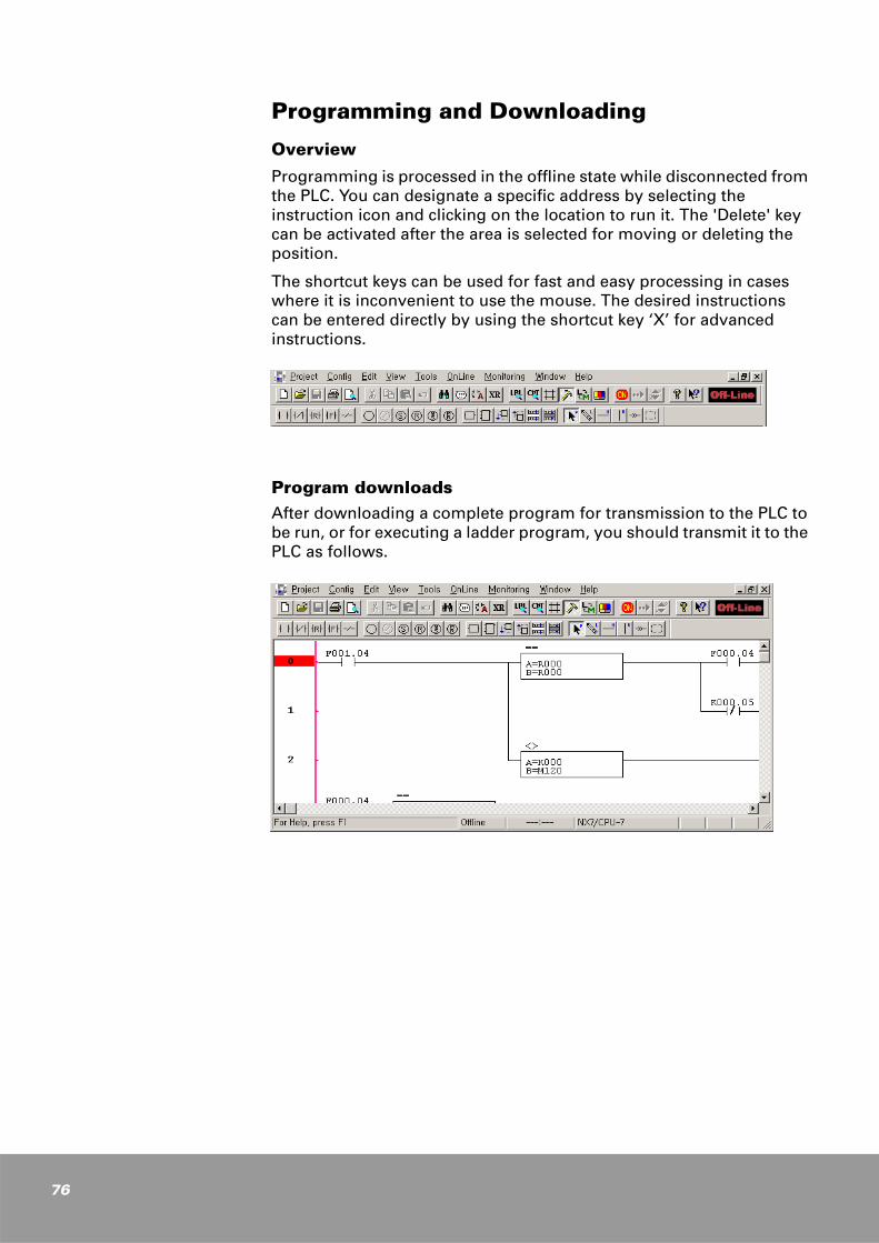
76
Programming and Downloading
Overview
Programming is processed in the offline state while disconnected from the PLC. You can designate a specific address by selecting the instruction icon and clicking on the location to run it. The 'Delete' key can be activated after the area is selected for moving or deleting the position.
The shortcut keys can be used for fast and easy processing in cases where it is inconvenient to use the mouse. The desired instructions can be entered directly by using the shortcut key ‘X’ for advanced instructions.
Program downloadsAfter downloading a complete program for transmission to the PLC to be run, or for executing a ladder program, you should transmit it to the PLC as follows.

First, set the PLC operation switch to PROG, and select the `Online' button from the displayed icons. Select 'WinGPC==>PLC (W)...' from the Online menu.
Program Monitoring
OverviewWhen monitoring a program transmitted to the PLC, you may check the status of the contact point or operation by selecting the “Ladder Monitoring” from the “Monitoring” menu, as shown in the right figure.
To display the ladder program status as shown in the figure below, the same program must be installed on the PC, and it will convert to the ladder status through the normal programming process.
If the I/O contact point status does not have a problem, set the operation switch to ‘RUN’. The ‘RUN’ LED will be turned on, and the PLC will begin to run.
77

78
Program uploads
You can upload the program and export the program running on the PLC directly to the PC. The menu is selected in online mode. If a password has been set, this function will function after password validation.
Program verification
When checking the NX7 Series PLC programs on the PC, you must install the same program on the PC after uploading. Otherwise, you cannot verify and monitor the PLC programs. The figure below shows that the installed program is in the monitoring status.
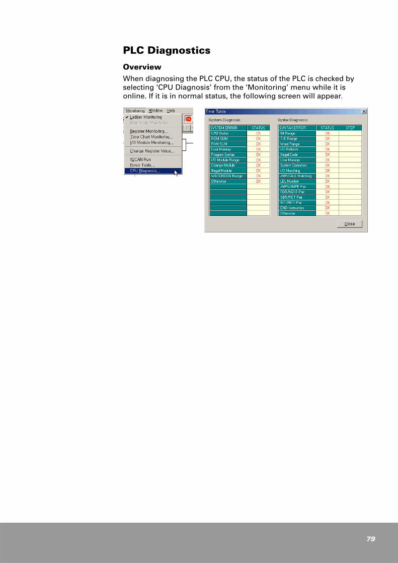
PLC Diagnostics
OverviewWhen diagnosing the PLC CPU, the status of the PLC is checked by selecting ‘CPU Diagnosis’ from the ‘Monitoring’ menu while it is online. If it is in normal status, the following screen will appear.
79

80
Error checkup
If any program error occurs, ‘FAIL’ appears on the ‘Program Syntax’ item in the system diagnosis table on the left side of the error information screen, and its relevant step number is shown in the Syntax Diagnosis table on the right side. Checking the error code is critical to taking quick and appropriate action to correct the problem.
The figure below displays an error that appeared because of a wrong designation of the input/output address. In other words, the error occurred because the output point to step #2 was assigned as an input address. If this occurs, the error lamp turns on, and the CPU stops.

Using a Password
Overview
You can set the password to protect programs stored in the PLC CPU. To set or change the password, go online with your WinGPC, click Online | System Information | Password and then enter a new password. The password may include any combination of numbers and special characters.
However, we recommend using alphanumeric characters. Once the password is set, if you do not enter the correct password, you cannot access to the program, i.e., you cannot upload the program, and you cannot change or disable the password.
Disabling a password
Enter '0000' to disable the password function. Then,you will not be prompted to enter the password when you go online.
81

82

NX7
Publicatio
Series Controller
OE MAX ControlsTrademarks not belonging to OE MAX Controls are
www.oemax.com property of their respective companies.Copyright © 2004 OE MAX Controlsn NX70-UM001A-EN-P-2004.12